Embed Size (px)
Citation preview
Global Maximum Power Point Tracking (MPPT) Technique in DC –DC Boost Converter Solar Photovoltaic Array Under Partially Shaded
Condition S.SATHISH KUMAR, C.NAGARAJAN
RESEARCH SCHOLAR, PROFESSOR/EEE Anna University, Anna University
GRT Institute of Engineering & Technology, Muthayammal College of Engineering INDIA
[email protected],[email protected] Abstract: - Today, with the focus on greener sources of power, PV has become an important source of power for a wide range of applications. Improvements in converting light energy into electrical energy as well as the cost reductions have helped create this growth. Even with higher efficiency and lower cost, the goal remains to maximize the power from the PV system under various lighting conditions. This paper describes a design and validation of a Maximum Power Point Tracking (MPPT) capable of tracking the true Global Maximum Power Point (GMPP) in the presence of other local maxima. The proposed system tracks Maximum Power Point (MPP) without the use of costly components such as signal converters and microprocessors thereby increasing the compactness of the system
Key-Words: - Photovoltaic module, MPPT, boost converter, Global Dithering Algorithm, simulation.
1 Introduction
To improve the conversion efficiency of the PV System, a technique is adopted which is known as Maximum power point tracking. MPPT make the PV system to operate at its maximum power. As such, many MPPT techniques have been introduced and implemented. By conventional popular MPPT methods, it’s easier to find the maximum power in nonlinear P-V curve under uniform insulation, as there will be single maxima. However, under partially shaded conditions, these MPPTs can fail to track the real MPP because of the multiple local maxima which can be appeared on P-V characteristic curve.
On the impact of partial shading on PV panels and the failure of the conventional MPPT techniques during partial shading, several research articles have been archived. Some of the researchers have tried global search algorithm to find global maxima with the use of processors. This project involves developing a compact MPPT DC-DC converter which uses local dithering algorithm to obtain the local maximum power while ensuring that real global maximum power is always tracked with the help of global search algorithm. This method presented in this paper avoids the usage of processor instead it proposes simple circuit components to establish GMPPT algorithm.
2 Modeling of Photovoltaic Cell
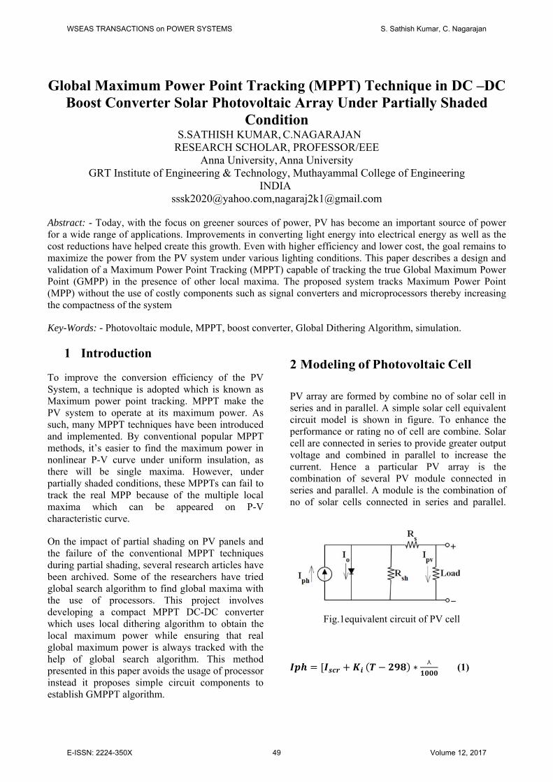
PV array are formed by combine no of solar cell in series and in parallel. A simple solar cell equivalent circuit model is shown in figure. To enhance the performance or rating no of cell are combine. Solar cell are connected in series to provide greater output voltage and combined in parallel to increase the current. Hence a particular PV array is the combination of several PV module connected in series and parallel. A module is the combination of no of solar cells connected in series and parallel.
Fig.1equivalent circuit of PV cell
∗⋏ (1)
WSEAS TRANSACTIONS on POWER SYSTEMS S. Sathish Kumar, C. Nagarajan
E-ISSN: 2224-350X 49 Volume 12, 2017
Reverses saturation current of the module:
1 (2)
Saturation current of the module:
(3)
The current output of PV module:
∗ exp∗
1 (4)
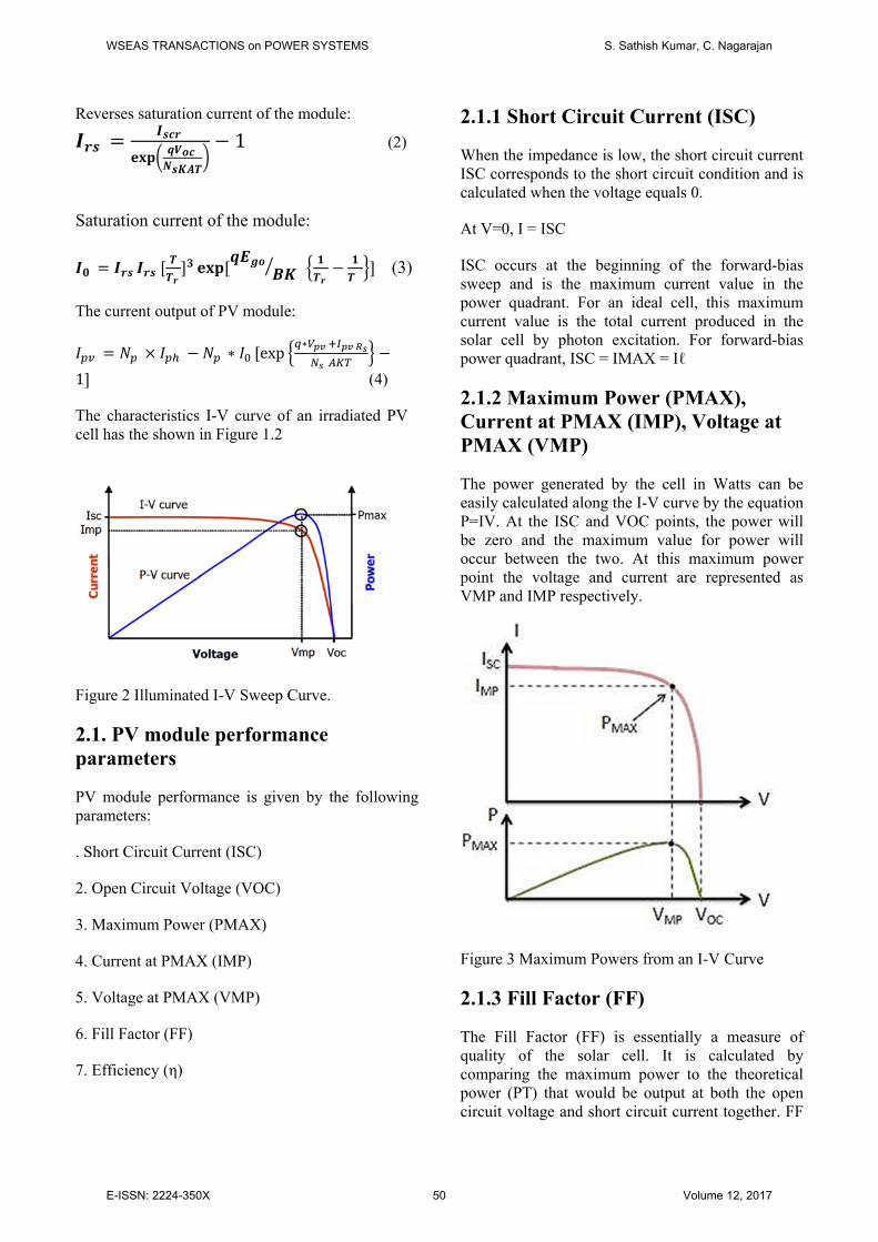
The characteristics I-V curve of an irradiated PV cell has the shown in Figure 1.2
Figure 2 Illuminated I-V Sweep Curve.
2.1. PV module performance parameters
PV module performance is given by the following parameters:
. Short Circuit Current (ISC)
2. Open Circuit Voltage (VOC)
3. Maximum Power (PMAX)
4. Current at PMAX (IMP)
5. Voltage at PMAX (VMP)
6. Fill Factor (FF)
7. Efficiency (η)
2.1.1 Short Circuit Current (ISC)
When the impedance is low, the short circuit current ISC corresponds to the short circuit condition and is calculated when the voltage equals 0.
At V=0, I = ISC
ISC occurs at the beginning of the forward-bias sweep and is the maximum current value in the power quadrant. For an ideal cell, this maximum current value is the total current produced in the solar cell by photon excitation. For forward-bias power quadrant, ISC = IMAX = Iℓ
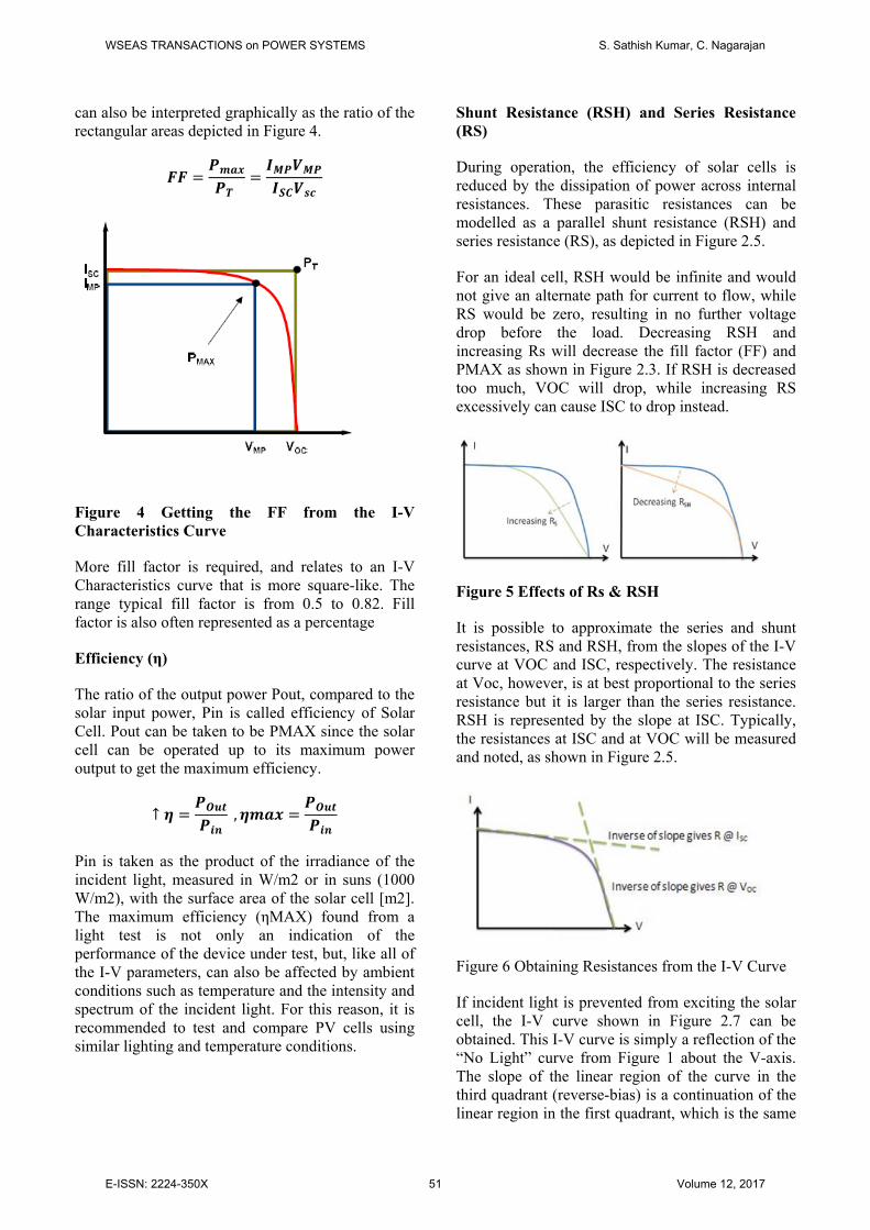
2.1.2 Maximum Power (PMAX), Current at PMAX (IMP), Voltage at PMAX (VMP)
The power generated by the cell in Watts can be easily calculated along the I-V curve by the equation P=IV. At the ISC and VOC points, the power will be zero and the maximum value for power will occur between the two. At this maximum power point the voltage and current are represented as VMP and IMP respectively.
Figure 3 Maximum Powers from an I-V Curve
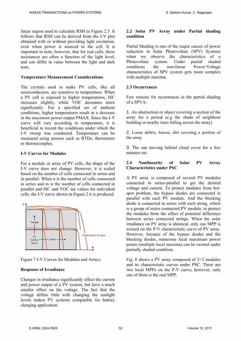
2.1.3 Fill Factor (FF)
The Fill Factor (FF) is essentially a measure of quality of the solar cell. It is calculated by comparing the maximum power to the theoretical power (PT) that would be output at both the open circuit voltage and short circuit current together. FF
WSEAS TRANSACTIONS on POWER SYSTEMS S. Sathish Kumar, C. Nagarajan
E-ISSN: 2224-350X 50 Volume 12, 2017
can also be interpreted graphically as the ratio of the rectangular areas depicted in Figure 4.
Figure 4 Getting the FF from the I-V Characteristics Curve
More fill factor is required, and relates to an I-V Characteristics curve that is more square-like. The range typical fill factor is from 0.5 to 0.82. Fill factor is also often represented as a percentage
Efficiency (η)
The ratio of the output power Pout, compared to the solar input power, Pin is called efficiency of Solar Cell. Pout can be taken to be PMAX since the solar cell can be operated up to its maximum power output to get the maximum efficiency.
↑ ,
Pin is taken as the product of the irradiance of the incident light, measured in W/m2 or in suns (1000 W/m2), with the surface area of the solar cell [m2]. The maximum efficiency (ηMAX) found from a light test is not only an indication of the performance of the device under test, but, like all of the I-V parameters, can also be affected by ambient conditions such as temperature and the intensity and spectrum of the incident light. For this reason, it is recommended to test and compare PV cells using similar lighting and temperature conditions.
Shunt Resistance (RSH) and Series Resistance (RS)
During operation, the efficiency of solar cells is reduced by the dissipation of power across internal resistances. These parasitic resistances can be modelled as a parallel shunt resistance (RSH) and series resistance (RS), as depicted in Figure 2.5.
For an ideal cell, RSH would be infinite and would not give an alternate path for current to flow, while RS would be zero, resulting in no further voltage drop before the load. Decreasing RSH and increasing Rs will decrease the fill factor (FF) and PMAX as shown in Figure 2.3. If RSH is decreased too much, VOC will drop, while increasing RS excessively can cause ISC to drop instead.
Figure 5 Effects of Rs & RSH
It is possible to approximate the series and shunt resistances, RS and RSH, from the slopes of the I-V curve at VOC and ISC, respectively. The resistance at Voc, however, is at best proportional to the series resistance but it is larger than the series resistance. RSH is represented by the slope at ISC. Typically, the resistances at ISC and at VOC will be measured and noted, as shown in Figure 2.5.
Figure 6 Obtaining Resistances from the I-V Curve
If incident light is prevented from exciting the solar cell, the I-V curve shown in Figure 2.7 can be obtained. This I-V curve is simply a reflection of the “No Light” curve from Figure 1 about the V-axis. The slope of the linear region of the curve in the third quadrant (reverse-bias) is a continuation of the linear region in the first quadrant, which is the same
WSEAS TRANSACTIONS on POWER SYSTEMS S. Sathish Kumar, C. Nagarajan
E-ISSN: 2224-350X 51 Volume 12, 2017
linear region used to calculate RSH in Figure 2.5. It follows that RSH can be derived from the I-V plot obtained with or without providing light excitation, even when power is sourced to the cell. It is important to note, however, that for real cells, these resistances are often a function of the light level, and can differ in value between the light and dark tests.
Temperature Measurement Considerations
The crystals used to make PV cells, like all semiconductors, are sensitive to temperature. When a PV cell is exposed to higher temperatures, ISC increases slightly, while VOC decreases more significantly. For a specified set of ambient conditions, higher temperatures result in a decrease in the maximum power output PMAX. Since the I-V curve will vary according to temperature, it is beneficial to record the conditions under which the I-V sweep was conducted. Temperature can be measured using sensors such as RTDs, thermistors or thermocouples.
I-V Curves for Modules
For a module or array of PV cells, the shape of the I-V curve does not change. However, it is scaled based on the number of cells connected in series and in parallel. When n is the number of cells connected in series and m is the number of cells connected in parallel and ISC and VOC are values for individual cells, the I-V curve shown in Figure 2.6 is produced.
Figure 7 I-V Curves for Modules and Arrays
Response of Irradiance
Changes in irradiance significantly affect the current and power output of a PV system, but have a much smaller effect on the voltage. The fact that the voltage differs little with changing the sunlight levels makes PV systems compatible for battery charging application.
2.2 Solar PV Array under Partial shading condition
Partial Shading is one of the major causes of power reduction in Solar Photovoltaic (SPV) Systems when we observe the characteristics of a Photovoltaic system. Under partial shaded conditions the non-linear Power-Voltage characteristics of SPV system gets more complex with multiple maxima.
2.3 Occurrences
Few reasons for occurrences in the partial shading of a SPVA:
1. An obstruction or object covering a section of the array for a period (e.g the shade of neighbour building or nearby trees falling across the array)
2. Loose debris, leaves, dirt covering a portion of the array
3. The sun moving behind cloud cover for a few minutes etc.
2.4 Nonlinearity of Solar PV Array Characteristics under PSC
A PV array is composed of several PV modules connected in series-parallel to get the desired voltage and current. To protect modules from hot-spot problem, the bypass diodes are connected in parallel with each PV module. And the blocking diode is connected in series with each string, which is a group of series connected PV module, to protect the modules from the effect of potential difference between series connected strings. When the solar irradiance on PV array is identical, only one MPP is existed on the P-V characteristic curve of PV array. However, because of the bypass diodes and the blocking diodes, numerous local maximum power points (multiple local maxima) can be existed under partially shaded condition.
Fig. 8 shows a PV array composed of 3×2 modules and its characteristic curves under PSC. There are two local MPPs on the P-V curve; however, only one of them is the real MPP.
WSEAS TRANSACTIONS on POWER SYSTEMS S. Sathish Kumar, C. Nagarajan
E-ISSN: 2224-350X 52 Volume 12, 2017
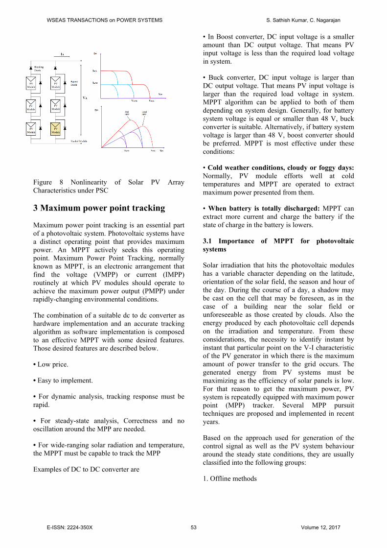
Figure 8 Nonlinearity of Solar PV Array Characteristics under PSC
3 Maximum power point tracking
Maximum power point tracking is an essential part of a photovoltaic system. Photovoltaic systems have a distinct operating point that provides maximum power. An MPPT actively seeks this operating point. Maximum Power Point Tracking, normally known as MPPT, is an electronic arrangement that find the voltage (VMPP) or current (IMPP) routinely at which PV modules should operate to achieve the maximum power output (PMPP) under rapidly-changing environmental conditions.
The combination of a suitable dc to dc converter as hardware implementation and an accurate tracking algorithm as software implementation is composed to an effective MPPT with some desired features. Those desired features are described below.
• Low price.
• Easy to implement.
• For dynamic analysis, tracking response must be rapid.
• For steady-state analysis, Correctness and no oscillation around the MPP are needed.
• For wide-ranging solar radiation and temperature, the MPPT must be capable to track the MPP
Examples of DC to DC converter are
• In Boost converter, DC input voltage is a smaller amount than DC output voltage. That means PV input voltage is less than the required load voltage in system.
• Buck converter, DC input voltage is larger than DC output voltage. That means PV input voltage is larger than the required load voltage in system. MPPT algorithm can be applied to both of them depending on system design. Generally, for battery system voltage is equal or smaller than 48 V, buck converter is suitable. Alternatively, if battery system voltage is larger than 48 V, boost converter should be preferred. MPPT is most effective under these conditions:
• Cold weather conditions, cloudy or foggy days: Normally, PV module efforts well at cold temperatures and MPPT are operated to extract maximum power presented from them.
• When battery is totally discharged: MPPT can extract more current and charge the battery if the state of charge in the battery is lowers.
3.1 Importance of MPPT for photovoltaic systems
Solar irradiation that hits the photovoltaic modules has a variable character depending on the latitude, orientation of the solar field, the season and hour of the day. During the course of a day, a shadow may be cast on the cell that may be foreseen, as in the case of a building near the solar field or unforeseeable as those created by clouds. Also the energy produced by each photovoltaic cell depends on the irradiation and temperature. From these considerations, the necessity to identify instant by instant that particular point on the V-I characteristic of the PV generator in which there is the maximum amount of power transfer to the grid occurs. The generated energy from PV systems must be maximizing as the efficiency of solar panels is low. For that reason to get the maximum power, PV system is repeatedly equipped with maximum power point (MPP) tracker. Several MPP pursuit techniques are proposed and implemented in recent years.
Based on the approach used for generation of the control signal as well as the PV system behaviour around the steady state conditions, they are usually classified into the following groups:
1. Offline methods
WSEAS TRANSACTIONS on POWER SYSTEMS S. Sathish Kumar, C. Nagarajan
E-ISSN: 2224-350X 53 Volume 12, 2017
Open circuit voltage (OCV) method Short circuit current method (SCC) Artificial intelligence
2. Online methods Perturbation and observation method (P&O) Extremum seeking control method (ESC) Incremental conductance method
(IncCond).
3. Hybrid methods
Figure 9 Need of MPPT
3.2. Perturb and Observe (P&O)
The most commonly used MPPT algorithm is P&O method. This algorithm uses simple feedback arrangement and little measured parameters. In this approach, the module voltage is periodically given a perturbation and the corresponding output power is compared with that at the previous perturbing cycle. In this algorithm a slight perturbation is introduce to the system. This perturbation causes the power of the solar module various. If the power increases due to the perturbation then the perturbation is continued in the same direction. After the peak power is reached the power at the MPP is zero and next instant decreases and hence after that the perturbation reverses. When the stable condition is arrived the algorithm oscillates around the peak power point. In order to maintain the power variation small the perturbation size is remain very small. The technique is advanced in such a style that it sets a reference voltage of the module corresponding to the peak voltage of the module. A PI controller then acts to transfer the operating point of the module to that particular voltage level. It is observed some power loss due to this perturbation also the fails to track the maximum power under fast
changing atmospheric conditions. But remain this technique is very popular and simple
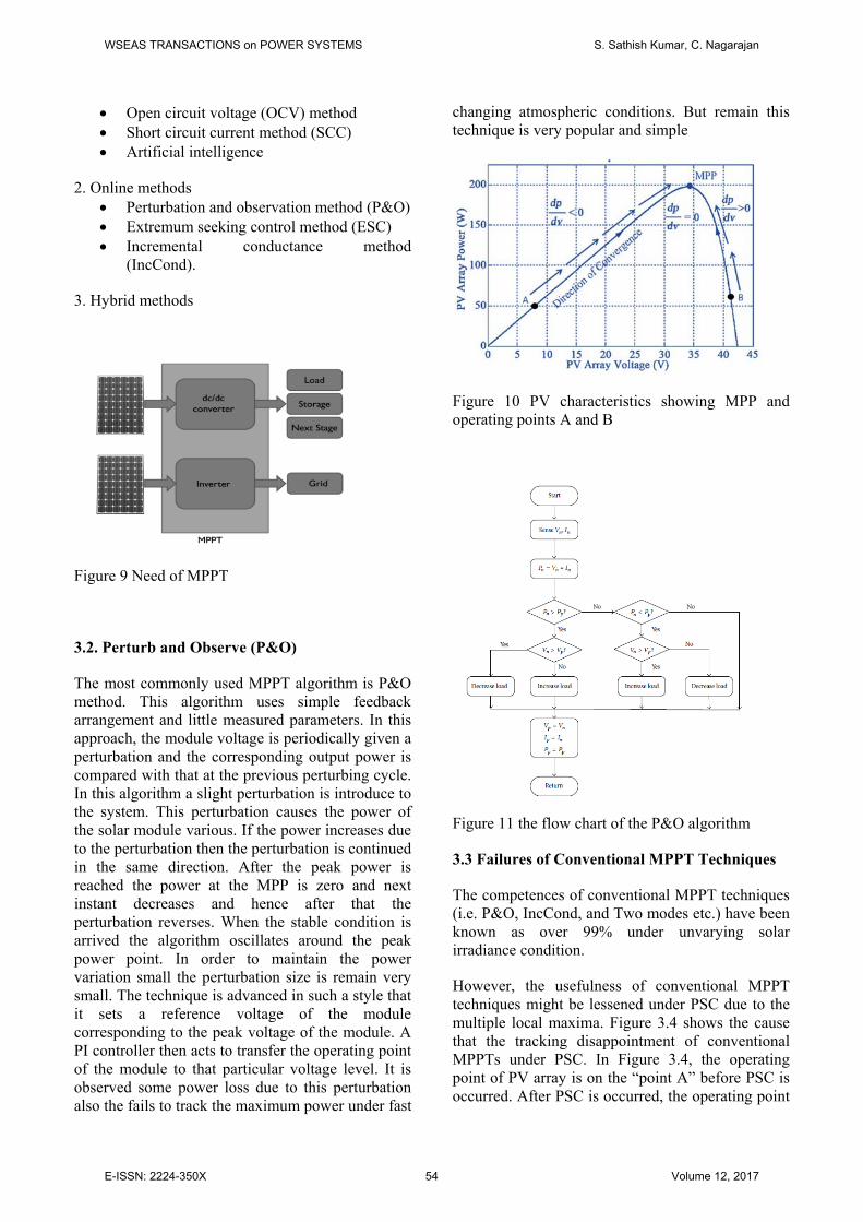
Figure 10 PV characteristics showing MPP and operating points A and B
Figure 11 the flow chart of the P&O algorithm
3.3 Failures of Conventional MPPT Techniques
The competences of conventional MPPT techniques (i.e. P&O, IncCond, and Two modes etc.) have been known as over 99% under unvarying solar irradiance condition.
However, the usefulness of conventional MPPT techniques might be lessened under PSC due to the multiple local maxima. Figure 3.4 shows the cause that the tracking disappointment of conventional MPPTs under PSC. In Figure 3.4, the operating point of PV array is on the “point A” before PSC is occurred. After PSC is occurred, the operating point
WSEAS TRANSACTIONS on POWER SYSTEMS S. Sathish Kumar, C. Nagarajan
E-ISSN: 2224-350X 54 Volume 12, 2017
is moved to “point B”. In this case, the real MPP is to be found on “point C”. Nevertheless, because of the conventional methods changes the operating point due to predetermined voltage reference step ( V), the operating point is oscillated on vicinity of “point B”. At the same time, the difference in power capacity between PC and PB is lost due to this MPPT failure. To prevent this power loss, MPPT methods have to move the operating point to “point C”.
Figure 12 Failure of MPPT in conventional method under PSC
Actually these methods have some drawbacks with complexity of method, tracking failure according to the real MPP position, and difficulties on the application to the installed power conditioning system. Besides, some methods include short-circuit or open-circuit condition that makes output power of PV array to be zero.
To improve the drawbacks of conventional methods, the requirements that have to be considered in MPPT method under PSC are deduced. The requirements are as follows;
1) It has to be applied to the installed power conditioning systems without additional circuits.
2) Under partial shading
3.4 DC-DC converters
DC to DC converters are used for converting one level of input voltage to other level of DC output voltage. DC-DC converters consist of inductor, capacitors and switches, DC-DC Converter interface with PV system are very essential for that we need a good converter. These converters play a role of charge controller, MPP trackers and PV interface with load. We have many types’ isolated and non-
isolated converters among that buck and boost non isolated DC-DC converters frequently use in literature, because of their easy structure and less components. Among these two boosts converter is advantageous.
Figure 13 DC-DC converters with the PV interface
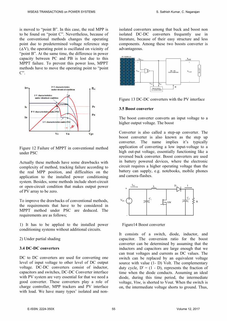
3.5 Boost converter
The boost converter converts an input voltage to a higher output voltage. The boost
Converter is also called a step-up converter. The boost converter is also known as the step up converter. The name implies it’s typically application of converting a low input-voltage to a high out-put voltage, essentially functioning like a reversed buck converter. Boost converters are used in battery powered devices, where the electronic circuit requires a higher operating voltage than the battery can supply, e.g. notebooks, mobile phones and camera-flashes.
Figure14 Boost converter
It consists of a switch, diode, inductor, and capacitor. The conversion ratio for the boost converter can be determined by assuming that the inductors and capacitors are large enough that we can treat voltages and currents as DC values. The switch can be replaced by an equivalent voltage source with value (1- D) Volt. The complementary duty cycle, D' = (1 - D), represents the fraction of time when the diode conducts. Assuming an ideal diode, during this time period, the intermediate voltage, Vsw, is shorted to Vout. When the switch is on, the intermediate voltage shorts to ground. Thus,
WSEAS TRANSACTIONS on POWER SYSTEMS S. Sathish Kumar, C. Nagarajan
E-ISSN: 2224-350X 55 Volume 12, 2017
its average value is equal to (1 - D) Vout. Since at DC the inductor can be replaced by a short, Vin = (1-D) Vout
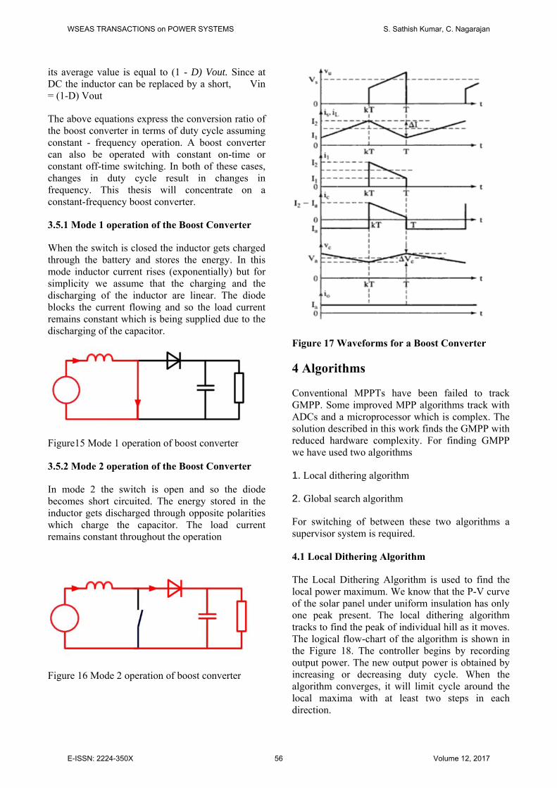
The above equations express the conversion ratio of the boost converter in terms of duty cycle assuming constant - frequency operation. A boost converter can also be operated with constant on-time or constant off-time switching. In both of these cases, changes in duty cycle result in changes in frequency. This thesis will concentrate on a constant-frequency boost converter.
3.5.1 Mode 1 operation of the Boost Converter
When the switch is closed the inductor gets charged through the battery and stores the energy. In this mode inductor current rises (exponentially) but for simplicity we assume that the charging and the discharging of the inductor are linear. The diode blocks the current flowing and so the load current remains constant which is being supplied due to the discharging of the capacitor.
Figure15 Mode 1 operation of boost converter
3.5.2 Mode 2 operation of the Boost Converter
In mode 2 the switch is open and so the diode becomes short circuited. The energy stored in the inductor gets discharged through opposite polarities which charge the capacitor. The load current remains constant throughout the operation
Figure 16 Mode 2 operation of boost converter
Figure 17 Waveforms for a Boost Converter
4 Algorithms
Conventional MPPTs have been failed to track GMPP. Some improved MPP algorithms track with ADCs and a microprocessor which is complex. The solution described in this work finds the GMPP with reduced hardware complexity. For finding GMPP we have used two algorithms
1. Local dithering algorithm
2. Global search algorithm
For switching of between these two algorithms a supervisor system is required.
4.1 Local Dithering Algorithm
The Local Dithering Algorithm is used to find the local power maximum. We know that the P-V curve of the solar panel under uniform insulation has only one peak present. The local dithering algorithm tracks to find the peak of individual hill as it moves. The logical flow-chart of the algorithm is shown in the Figure 18. The controller begins by recording output power. The new output power is obtained by increasing or decreasing duty cycle. When the algorithm converges, it will limit cycle around the local maxima with at least two steps in each direction.
WSEAS TRANSACTIONS on POWER SYSTEMS S. Sathish Kumar, C. Nagarajan
E-ISSN: 2224-350X 56 Volume 12, 2017
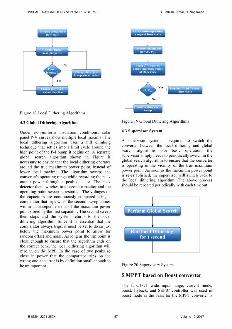
Figure 18 Local Dithering Algorithms
4.2 Global Dithering Algorithm
Under non-uniform insulation conditions, solar panel P-V curves show multiple local maxima. The local dithering algorithm uses a hill climbing technique that settles into a limit cycle around the high point of the P-I bump it begins on. A separate global search algorithm shown in Figure is necessary to ensure that the local dithering operates around the true maximum power point, instead of lower local maxima. The algorithm sweeps the converter's operating range while recording the peak output power through a peak detector. The peak detector then switches to a second capacitor and the operating point sweep is restarted. The voltages on the capacitors are continuously compared using a comparator that trips when the second sweep comes within an acceptable delta of the maximum power point stored by the first capacitor. The second sweep then stops and the system returns to the local dithering algorithm. Since it is essential that the comparator always trips, it must be set to do so just below the maximum power point to allow for random offset and noise. As long as the trip point is close enough to ensure that the algorithm ends on the correct peak, the local dithering algorithm will zero in on the MPP. In the case of two peaks so close in power that the comparator trips on the wrong one, the error is by definition small enough to be unimportant.
Figure 19 Global Dithering Algorithms
4.3 Supervisor System
A supervisor system is required to switch the converter between the local dithering and global search algorithms. For basic operation, the supervisor simply needs to periodically switch in the global search algorithm to ensure that the converter is operating in the vicinity of the true maximum power point. As soon as the maximum power point is re-established, the supervisor will switch back to the local dithering algorithm. The above process should be repeated periodically with each timeout.
Figure 20 Supervisory System
5 MPPT based on Boost converter
The LTC1871 wide input range, current mode, boost, flyback, and SEPIC controller was used in boost mode as the basis for the MPPT converter is
WSEAS TRANSACTIONS on POWER SYSTEMS S. Sathish Kumar, C. Nagarajan
E-ISSN: 2224-350X 57 Volume 12, 2017
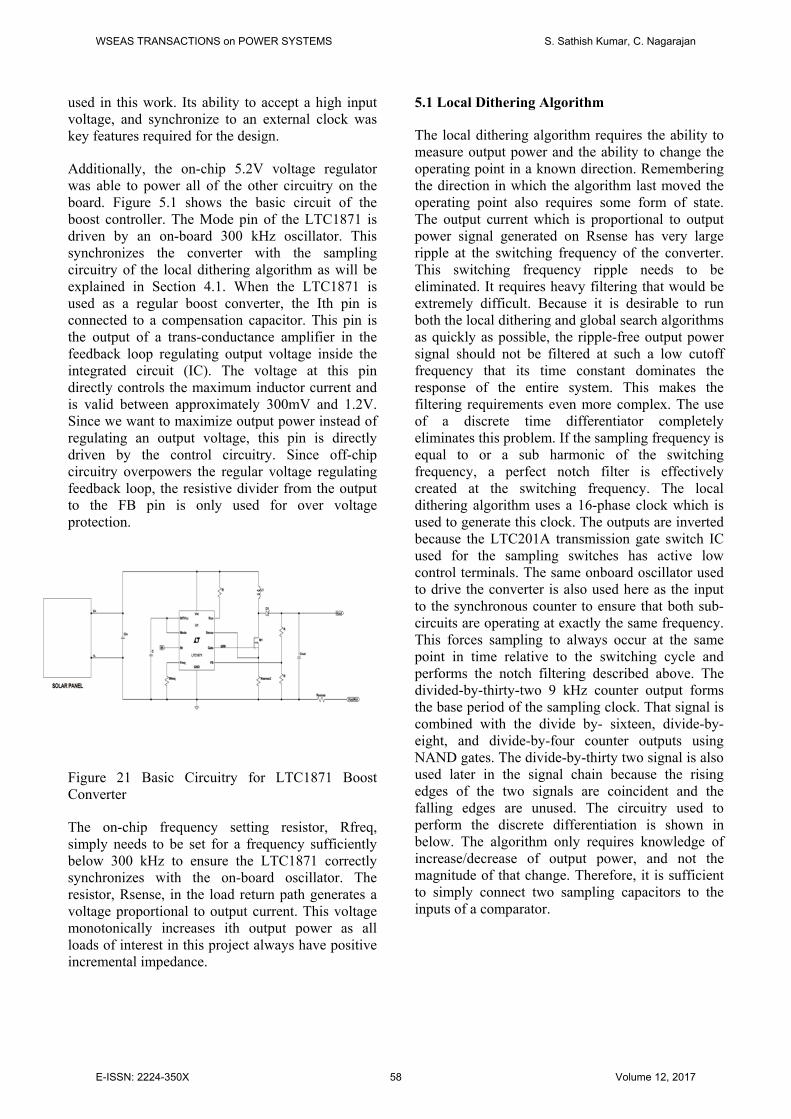
used in this work. Its ability to accept a high input voltage, and synchronize to an external clock was key features required for the design.
Additionally, the on-chip 5.2V voltage regulator was able to power all of the other circuitry on the board. Figure 5.1 shows the basic circuit of the boost controller. The Mode pin of the LTC1871 is driven by an on-board 300 kHz oscillator. This synchronizes the converter with the sampling circuitry of the local dithering algorithm as will be explained in Section 4.1. When the LTC1871 is used as a regular boost converter, the Ith pin is connected to a compensation capacitor. This pin is the output of a trans-conductance amplifier in the feedback loop regulating output voltage inside the integrated circuit (IC). The voltage at this pin directly controls the maximum inductor current and is valid between approximately 300mV and 1.2V. Since we want to maximize output power instead of regulating an output voltage, this pin is directly driven by the control circuitry. Since off-chip circuitry overpowers the regular voltage regulating feedback loop, the resistive divider from the output to the FB pin is only used for over voltage protection.
Figure 21 Basic Circuitry for LTC1871 Boost Converter
The on-chip frequency setting resistor, Rfreq, simply needs to be set for a frequency sufficiently below 300 kHz to ensure the LTC1871 correctly synchronizes with the on-board oscillator. The resistor, Rsense, in the load return path generates a voltage proportional to output current. This voltage monotonically increases ith output power as all loads of interest in this project always have positive incremental impedance.
5.1 Local Dithering Algorithm
The local dithering algorithm requires the ability to measure output power and the ability to change the operating point in a known direction. Remembering the direction in which the algorithm last moved the operating point also requires some form of state. The output current which is proportional to output power signal generated on Rsense has very large ripple at the switching frequency of the converter. This switching frequency ripple needs to be eliminated. It requires heavy filtering that would be extremely difficult. Because it is desirable to run both the local dithering and global search algorithms as quickly as possible, the ripple-free output power signal should not be filtered at such a low cutoff frequency that its time constant dominates the response of the entire system. This makes the filtering requirements even more complex. The use of a discrete time differentiator completely eliminates this problem. If the sampling frequency is equal to or a sub harmonic of the switching frequency, a perfect notch filter is effectively created at the switching frequency. The local dithering algorithm uses a 16-phase clock which is used to generate this clock. The outputs are inverted because the LTC201A transmission gate switch IC used for the sampling switches has active low control terminals. The same onboard oscillator used to drive the converter is also used here as the input to the synchronous counter to ensure that both sub-circuits are operating at exactly the same frequency. This forces sampling to always occur at the same point in time relative to the switching cycle and performs the notch filtering described above. The divided-by-thirty-two 9 kHz counter output forms the base period of the sampling clock. That signal is combined with the divide by- sixteen, divide-by-eight, and divide-by-four counter outputs using NAND gates. The divide-by-thirty two signal is also used later in the signal chain because the rising edges of the two signals are coincident and the falling edges are unused. The circuitry used to perform the discrete differentiation is shown in below. The algorithm only requires knowledge of increase/decrease of output power, and not the magnitude of that change. Therefore, it is sufficient to simply connect two sampling capacitors to the inputs of a comparator.
WSEAS TRANSACTIONS on POWER SYSTEMS S. Sathish Kumar, C. Nagarajan
E-ISSN: 2224-350X 58 Volume 12, 2017
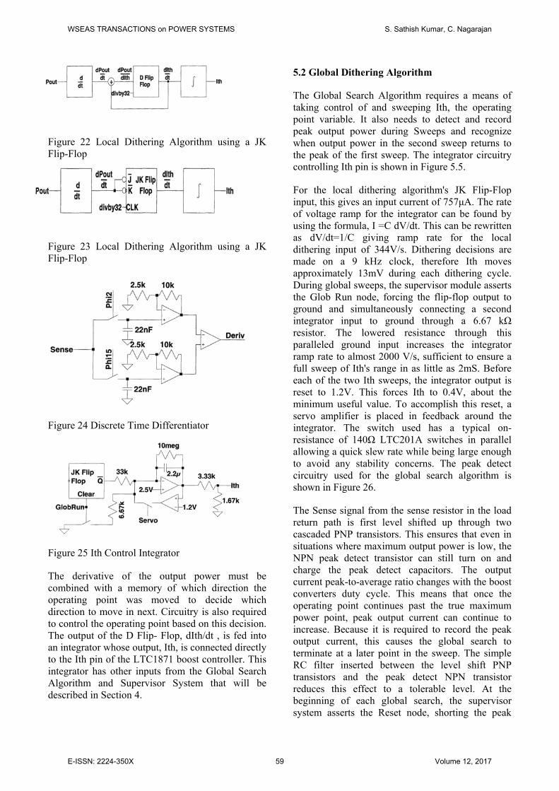
Figure 22 Local Dithering Algorithm using a JK Flip-Flop
Figure 23 Local Dithering Algorithm using a JK Flip-Flop
Figure 24 Discrete Time Differentiator
Figure 25 Ith Control Integrator
The derivative of the output power must be combined with a memory of which direction the operating point was moved to decide which direction to move in next. Circuitry is also required to control the operating point based on this decision. The output of the D Flip- Flop, dIth/dt , is fed into an integrator whose output, Ith, is connected directly to the Ith pin of the LTC1871 boost controller. This integrator has other inputs from the Global Search Algorithm and Supervisor System that will be described in Section 4.
5.2 Global Dithering Algorithm
The Global Search Algorithm requires a means of taking control of and sweeping Ith, the operating point variable. It also needs to detect and record peak output power during Sweeps and recognize when output power in the second sweep returns to the peak of the first sweep. The integrator circuitry controlling Ith pin is shown in Figure 5.5.
For the local dithering algorithm's JK Flip-Flop input, this gives an input current of 757μA. The rate of voltage ramp for the integrator can be found by using the formula, I =C dV/dt. This can be rewritten as dV/dt=1/C giving ramp rate for the local dithering input of 344V/s. Dithering decisions are made on a 9 kHz clock, therefore Ith moves approximately 13mV during each dithering cycle. During global sweeps, the supervisor module asserts the Glob Run node, forcing the flip-flop output to ground and simultaneously connecting a second integrator input to ground through a 6.67 kΩ resistor. The lowered resistance through this paralleled ground input increases the integrator ramp rate to almost 2000 V/s, sufficient to ensure a full sweep of Ith's range in as little as 2mS. Before each of the two Ith sweeps, the integrator output is reset to 1.2V. This forces Ith to 0.4V, about the minimum useful value. To accomplish this reset, a servo amplifier is placed in feedback around the integrator. The switch used has a typical on-resistance of 140Ω LTC201A switches in parallel allowing a quick slew rate while being large enough to avoid any stability concerns. The peak detect circuitry used for the global search algorithm is shown in Figure 26.
The Sense signal from the sense resistor in the load return path is first level shifted up through two cascaded PNP transistors. This ensures that even in situations where maximum output power is low, the NPN peak detect transistor can still turn on and charge the peak detect capacitors. The output current peak-to-average ratio changes with the boost converters duty cycle. This means that once the operating point continues past the true maximum power point, peak output current can continue to increase. Because it is required to record the peak output current, this causes the global search to terminate at a later point in the sweep. The simple RC filter inserted between the level shift PNP transistors and the peak detect NPN transistor reduces this effect to a tolerable level. At the beginning of each global search, the supervisor system asserts the Reset node, shorting the peak
WSEAS TRANSACTIONS on POWER SYSTEMS S. Sathish Kumar, C. Nagarajan
E-ISSN: 2224-350X 59 Volume 12, 2017
detect capacitors to ground. Then, when the sweep begins, PD1ON is asserted and the first capacitor is connected to the peak detector. PD1ON is de-asserted when the first sweep finishes. After Ith is served the second time, PD2ON is asserted and the second capacitor is connected to the peak detector. Both capacitors are always connected to a comparator whose output changes state during the second sweep when output power returns to the maximum recorded during the first sweep.
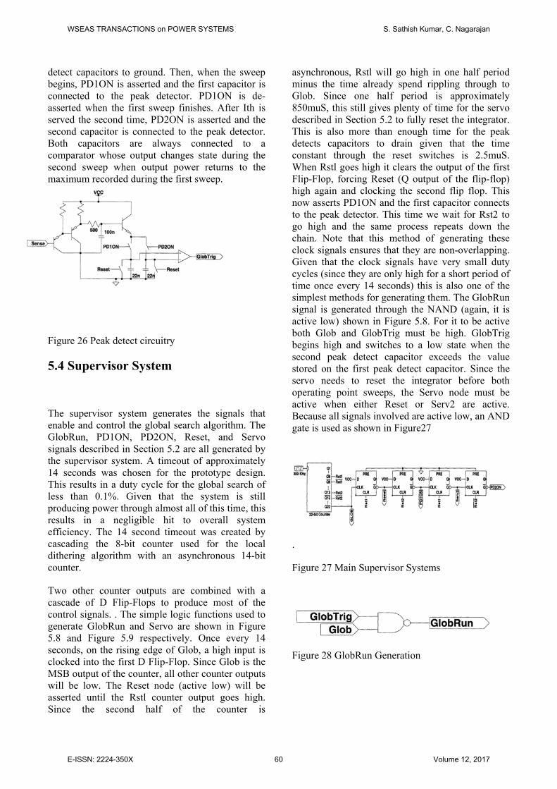
Figure 26 Peak detect circuitry
5.4 Supervisor System
The supervisor system generates the signals that enable and control the global search algorithm. The GlobRun, PD1ON, PD2ON, Reset, and Servo signals described in Section 5.2 are all generated by the supervisor system. A timeout of approximately 14 seconds was chosen for the prototype design. This results in a duty cycle for the global search of less than 0.1%. Given that the system is still producing power through almost all of this time, this results in a negligible hit to overall system efficiency. The 14 second timeout was created by cascading the 8-bit counter used for the local dithering algorithm with an asynchronous 14-bit counter.
Two other counter outputs are combined with a cascade of D Flip-Flops to produce most of the control signals. . The simple logic functions used to generate GlobRun and Servo are shown in Figure 5.8 and Figure 5.9 respectively. Once every 14 seconds, on the rising edge of Glob, a high input is clocked into the first D Flip-Flop. Since Glob is the MSB output of the counter, all other counter outputs will be low. The Reset node (active low) will be asserted until the Rstl counter output goes high. Since the second half of the counter is
asynchronous, Rstl will go high in one half period minus the time already spend rippling through to Glob. Since one half period is approximately 850muS, this still gives plenty of time for the servo described in Section 5.2 to fully reset the integrator. This is also more than enough time for the peak detects capacitors to drain given that the time constant through the reset switches is 2.5muS. When Rstl goes high it clears the output of the first Flip-Flop, forcing Reset (Q output of the flip-flop) high again and clocking the second flip flop. This now asserts PD1ON and the first capacitor connects to the peak detector. This time we wait for Rst2 to go high and the same process repeats down the chain. Note that this method of generating these clock signals ensures that they are non-overlapping. Given that the clock signals have very small duty cycles (since they are only high for a short period of time once every 14 seconds) this is also one of the simplest methods for generating them. The GlobRun signal is generated through the NAND (again, it is active low) shown in Figure 5.8. For it to be active both Glob and GlobTrig must be high. GlobTrig begins high and switches to a low state when the second peak detect capacitor exceeds the value stored on the first peak detect capacitor. Since the servo needs to reset the integrator before both operating point sweeps, the Servo node must be active when either Reset or Serv2 are active. Because all signals involved are active low, an AND gate is used as shown in Figure27
.
Figure 27 Main Supervisor Systems
Figure 28 GlobRun Generation
WSEAS TRANSACTIONS on POWER SYSTEMS S. Sathish Kumar, C. Nagarajan
E-ISSN: 2224-350X 60 Volume 12, 2017
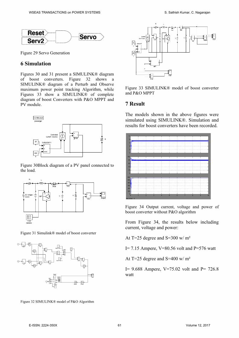
Figure 29 Servo Generation
6 Simulation
Figures 30 and 31 present a SIMULINK® diagram of boost converters. Figure 32 shows a SIMULINK® diagram of a Perturb and Observe maximum power point tracking Algorithm, while Figures 33 show a SIMULINK® of complete diagram of boost Converters with P&O MPPT and PV module.
Figure 30Block diagram of a PV panel connected to the load.
Figure 31 Simulink® model of boost converter
Figure 32 SIMULINK® model of P&O Algorithm
Figure 33 SIMULINK® model of boost converter and P&O MPPT
7 Result
The models shown in the above figures were simulated using SIMULINK®. Simulation and results for boost converters have been recorded.
Figure 34 Output current, voltage and power of boost converter without P&O algorithm
From Figure 34, the results below including current, voltage and power:
At T=25 degree and S=300 w/ m²
I= 7.15 Ampere, V=80.56 volt and P=576 watt
At T=25 degree and S=400 w/ m²
I= 9.688 Ampere, V=75.02 volt and P= 726.8 watt
WSEAS TRANSACTIONS on POWER SYSTEMS S. Sathish Kumar, C. Nagarajan
E-ISSN: 2224-350X 61 Volume 12, 2017
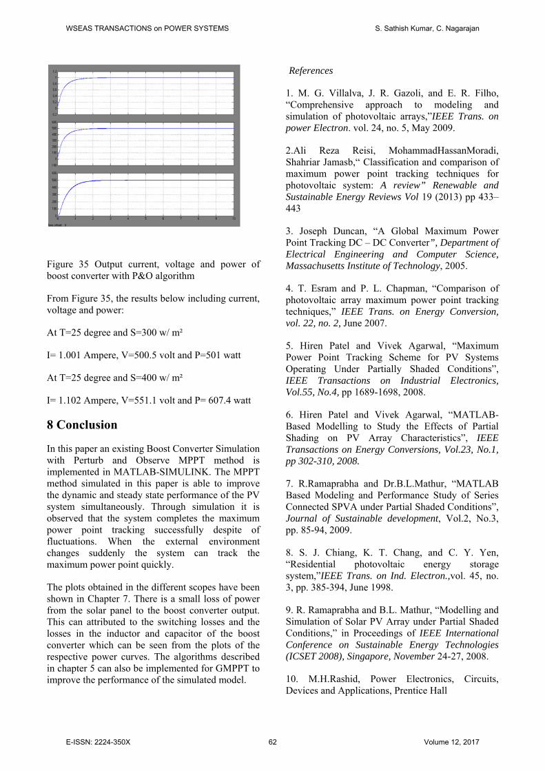
Figure 35 Output current, voltage and power of boost converter with P&O algorithm
From Figure 35, the results below including current, voltage and power:
At T=25 degree and S=300 w/ m²
I= 1.001 Ampere, V=500.5 volt and P=501 watt
At T=25 degree and S=400 w/ m²
I= 1.102 Ampere, V=551.1 volt and P= 607.4 watt
8 Conclusion
In this paper an existing Boost Converter Simulation with Perturb and Observe MPPT method is implemented in MATLAB-SIMULINK. The MPPT method simulated in this paper is able to improve the dynamic and steady state performance of the PV system simultaneously. Through simulation it is observed that the system completes the maximum power point tracking successfully despite of fluctuations. When the external environment changes suddenly the system can track the maximum power point quickly.
The plots obtained in the different scopes have been shown in Chapter 7. There is a small loss of power from the solar panel to the boost converter output. This can attributed to the switching losses and the losses in the inductor and capacitor of the boost converter which can be seen from the plots of the respective power curves. The algorithms described in chapter 5 can also be implemented for GMPPT to improve the performance of the simulated model.
References
1. M. G. Villalva, J. R. Gazoli, and E. R. Filho, “Comprehensive approach to modeling and simulation of photovoltaic arrays,”IEEE Trans. on power Electron. vol. 24, no. 5, May 2009.
2.Ali Reza Reisi, MohammadHassanMoradi, Shahriar Jamasb,“ Classification and comparison of maximum power point tracking techniques for photovoltaic system: A review” Renewable and Sustainable Energy Reviews Vol 19 (2013) pp 433–443
3. Joseph Duncan, “A Global Maximum Power Point Tracking DC – DC Converter”, Department of Electrical Engineering and Computer Science, Massachusetts Institute of Technology, 2005.
4. T. Esram and P. L. Chapman, “Comparison of photovoltaic array maximum power point tracking techniques,” IEEE Trans. on Energy Conversion, vol. 22, no. 2, June 2007.
5. Hiren Patel and Vivek Agarwal, “Maximum Power Point Tracking Scheme for PV Systems Operating Under Partially Shaded Conditions”, IEEE Transactions on Industrial Electronics, Vol.55, No.4, pp 1689-1698, 2008.
6. Hiren Patel and Vivek Agarwal, “MATLAB- Based Modelling to Study the Effects of Partial Shading on PV Array Characteristics”, IEEE Transactions on Energy Conversions, Vol.23, No.1, pp 302-310, 2008.
7. R.Ramaprabha and Dr.B.L.Mathur, “MATLAB Based Modeling and Performance Study of Series Connected SPVA under Partial Shaded Conditions”, Journal of Sustainable development, Vol.2, No.3, pp. 85-94, 2009.
8. S. J. Chiang, K. T. Chang, and C. Y. Yen, “Residential photovoltaic energy storage system,”IEEE Trans. on Ind. Electron.,vol. 45, no. 3, pp. 385-394, June 1998.
9. R. Ramaprabha and B.L. Mathur, “Modelling and Simulation of Solar PV Array under Partial Shaded Conditions,” in Proceedings of IEEE International Conference on Sustainable Energy Technologies (ICSET 2008), Singapore, November 24-27, 2008.
10. M.H.Rashid, Power Electronics, Circuits, Devices and Applications, Prentice Hall
WSEAS TRANSACTIONS on POWER SYSTEMS S. Sathish Kumar, C. Nagarajan
E-ISSN: 2224-350X 62 Volume 12, 2017