Embed Size (px)
Citation preview
Journal of Physics Conference Series
OPEN ACCESS
Grain contrast imaging in FIB and SEMTo cite this article S Canovic et al 2008 J Phys Conf Ser 126 012054
View the article online for updates and enhancements
You may also likeAcoustic interface contrast imagingJoost van der Neut Peter M van den BergJacob T Fokkema et al
-
X-ray phase-contrast imaging from pre-clinical applications towards clinicsAlberto Bravin Paola Coan and PekkaSuortti
-
X-ray phase contrast forCO2 microangiographyU Lundstroumlm D H Larsson A Burvall et al
-
Recent citationsThermally stable ultrafine grained copperinduced by CrBCrB2 microparticles withsurface nanofeatures via regular castingGongcheng Yao et al
-
Detection and quantification of precipitatesin 11ndash12 wt Cr steels using in-columnsecondary electron detectorsRobert G Byrne et al
-
Scanning transmission electronmicroscope mapping of electronictransport in polycrystalline BaTiO3 ceramiccapacitorsW A Hubbard et al
-
This content was downloaded from IP address 22010053116 on 22102021 at 1009
Grain contrast imaging in FIB and SEM
S Canovic1 T Jonsson and M Halvarsson
Microscopy and Microanalysis Department of Applied Physics Chalmers University of Technology SE-412 96 Goumlteborg Sweden
E-mail seadcanovicchalmersse
Abstract Grain contrast imaging can be performed with several techniques In order to be able to choose the most suitable one it is important to know which techniques are available and also to be aware of the strengths and weaknesses of each technique In this work the grain contrast imaging is performed with secondary electrons backscattered electrons forward scattered electrons transmitted electrons in the scanning electron microscope and with secondary electrons in the focused ion beam instrument The advantages and disadvantages of each method are discussed in order to make it easier to choose the most appropriate technique for grain contrast imaging
1 Introduction Grain contrast imaging can be performed by using a wide range of techniques and choosing the most suitable technique is not a straightforward task Historically etching and light microscopy has been used for imaging grain contrast Instead of photons electrons and ions can be used for imaging with a better resolution The most widely used imaging techniques where electrons and ions are used as imaging sources are scanning electron microscopy (SEM) and focused ion beam microscopy (FIB) respectively Imaging with secondary electrons (SE) backscattered electrons (BSE) and forward scattered electrons (FSE) are the most commonly used modes for imaging grain contrast in the SEM Another way to image grain contrast with high spatial resolution is by using thin foil specimens instead of bulk specimens ie scanning transmission electron microscopy (STEM) in the SEM
The aim of this paper is to illustrate grain contrast imaging with the techniques mentioned above and also to discuss the strengths and weaknesses of each technique
2 Experimental Three different samples have been used in this work These are (i) a κ-Al2O3TiC multilayer coating deposited on cemented carbide by using chemical vapour deposition (CVD) (ii) an oxidized pure iron sample with a thick iron oxide scale formed after oxidation in oxygen at 600degC for 1 hour and (iii) a Ti(CN) coating deposited on cemented carbide by using moderate temperature (MT) CVD
Two different instruments have been used (i) a Leo Ultra 55 FEG SEM equipped with an Everhart-Thornley (E-T) SE detector a solid state BSE detector an in-lens SE detector an FSE detector (mounted on a Nordlys electron backscattered detector (EBSD)) and a STEM detector and (ii) an FEI 200 THP FIB with a secondary electron detector 1 To whom any correspondence should be addressed
Electron Microscopy and Analysis Group Conference 2007 (EMAG 2007) IOP PublishingJournal of Physics Conference Series 126 (2008) 012054 doi1010881742-65961261012054
ccopy 2008 IOP Publishing Ltd 1
3 Results and Discussion
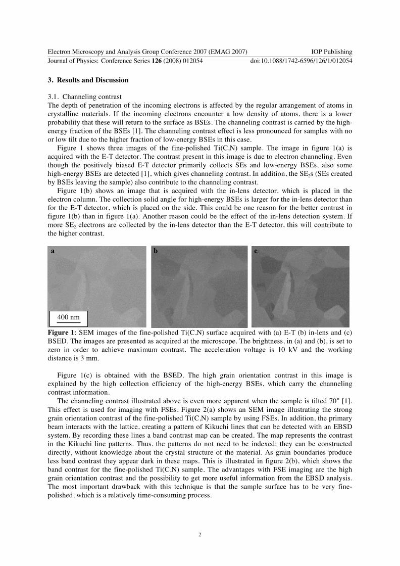
31 Channeling contrast The depth of penetration of the incoming electrons is affected by the regular arrangement of atoms in crystalline materials If the incoming electrons encounter a low density of atoms there is a lower probability that these will return to the surface as BSEs The channeling contrast is carried by the high-energy fraction of the BSEs [1] The channeling contrast effect is less pronounced for samples with no or low tilt due to the higher fraction of low-energy BSEs in this case
Figure 1 shows three images of the fine-polished Ti(CN) sample The image in figure 1(a) is acquired with the E-T detector The contrast present in this image is due to electron channeling Even though the positively biased E-T detector primarily collects SEs and low-energy BSEs also some high-energy BSEs are detected [1] which gives channeling contrast In addition the SE2s (SEs created by BSEs leaving the sample) also contribute to the channeling contrast
Figure 1(b) shows an image that is acquired with the in-lens detector which is placed in the electron column The collection solid angle for high-energy BSEs is larger for the in-lens detector than for the E-T detector which is placed on the side This could be one reason for the better contrast in figure 1(b) than in figure 1(a) Another reason could be the effect of the in-lens detection system If more SE2 electrons are collected by the in-lens detector than the E-T detector this will contribute to the higher contrast
Figure 1 SEM images of the fine-polished Ti(CN) surface acquired with (a) E-T (b) in-lens and (c) BSED The images are presented as acquired at the microscope The brightness in (a) and (b) is set to zero in order to achieve maximum contrast The acceleration voltage is 10 kV and the working distance is 3 mm
Figure 1(c) is obtained with the BSED The high grain orientation contrast in this image is
explained by the high collection efficiency of the high-energy BSEs which carry the channeling contrast information
The channeling contrast illustrated above is even more apparent when the sample is tilted 70deg [1] This effect is used for imaging with FSEs Figure 2(a) shows an SEM image illustrating the strong grain orientation contrast of the fine-polished Ti(CN) sample by using FSEs In addition the primary beam interacts with the lattice creating a pattern of Kikuchi lines that can be detected with an EBSD system By recording these lines a band contrast map can be created The map represents the contrast in the Kikuchi line patterns Thus the patterns do not need to be indexed they can be constructed directly without knowledge about the crystal structure of the material As grain boundaries produce less band contrast they appear dark in these maps This is illustrated in figure 2(b) which shows the band contrast for the fine-polished Ti(CN) sample The advantages with FSE imaging are the high grain orientation contrast and the possibility to get more useful information from the EBSD analysis The most important drawback with this technique is that the sample surface has to be very fine-polished which is a relatively time-consuming process
a b c
400 nm
Electron Microscopy and Analysis Group Conference 2007 (EMAG 2007) IOP PublishingJournal of Physics Conference Series 126 (2008) 012054 doi1010881742-65961261012054
2
Figure 2 (a) an SEM image of the fine-polished Ti(CN) surface acquired with FSEs (b) Band contrast of an EBSD pattern
In order to investigate the resolution of grain contrast images of samples that are not tilted a series
of images were acquired Figure 3 shows the fine-polished Ti(CN) sample viewed at 200 kX magnification Figure 3(a) (in-lens 10 kV) and 3(b) (BSED 10 kV) both show relatively high resolution in the order of 10 nm As mentioned above the channeling contrast is carried by the high-energy BSEs This means that only BSEs from the upper part of the pear-shaped interaction volume are contributing to the channeling contrast If the acceleration voltage is increased to 30 kV (from 10 kV) the resolution does not decrease significantly as is seen in figure 3(c) (BSED 30 kV) Although the total interaction volume increases the upper part of the interaction volume does not increase considerably This leads to only a slight loss in resolution in the grain contrast BSED image obtained at the higher voltage However the contrast is lower in figure 3(c) which could depend on a lower fraction of high-energy BSEs for higher acceleration voltage
Figure 3 SEM images of the fine-polished Ti(CN) surface acquired with (a) in-lens (10 kV) (b) BSED (10 kV) and (c) BSED (30 kV) The working distance is 3 mm
The procedure for SE and BSE imaging is fast and straightforward One disadvantage for the in-lens SE images is the problem with contamination during acquisition As the in-lens SE detector is very surface sensitive contamination will be very apparent in the images This means that the samples have to be cleaned carefully (eg with a plasma cleaner) and also the microscope chamber has to be clean
32 Other contrast mechanisms Another way to image grains with high spatial resolution in the SEM is by imaging thin foil specimens instead of bulk specimens with a STEM detector This leads to a reduction of the interaction volume without reducing the acceleration voltage The STEM unit used in this work consists of an electron detector with the ability of bright and dark field imaging A STEM bright field image of the Ti(CN) coating (figure 4) exhibits a high grain orientation contrast The use of high primary beam energies causes low aberration which results in high-resolution (lt 1 nm) images [2] A disadvantage is that the production of a thin foil specimen is relatively time-consuming
a b c
a b
150 nm
5 microm 4 microm
Electron Microscopy and Analysis Group Conference 2007 (EMAG 2007) IOP PublishingJournal of Physics Conference Series 126 (2008) 012054 doi1010881742-65961261012054
3
Figure 4 A STEM image acquired at 30 kV acceleration voltage of the Ti(CN) coating showing a high grain orientation contrast
Due to its high spatial resolution the FIB can be used as an imaging tool Figure 5(a) shows a FIB
image of an ion-milled cross section of iron oxide The grain orientation contrast in this image is caused by the channeling of the incident ions between lattice planes of the specimen [3] This means that different crystal orientations affect the number of secondary electrons escaping from the specimen which makes the different grains appear with different contrast However FIB is not always suitable for imaging grain orientation contrast Figure 5(b) shows a FIB image of a κ-Al2O3TiC multilayer coating No grain orientation contrast is visible in the thicker dark κ-Al2O3 layers which are polycrystalline as shown in the TEM micrograph in figure 5(c) Some advantages of using the FIB are the relatively good spatial resolution (~5 nm) and the high grain orientation contrast for many materials Some disadvantages are the difficulties of imaging non-conducting samples and also the damage created by the ion beam impact on the samples
Figure 5 (a) A FIB image of an ion-milled cross section of iron oxide (b) a FIB image of a κ-Al2O3TiC multilayer coating (c) a TEM micrograph showing two polycrystalline κ-Al2O3 layers
4 Concluding remarks There are several factors influencing the choice of method for grain contrast imaging One important factor to be considered is the type of material to be imaged For example the FIB cannot be used for imaging too non-conducting samples Another determining factor is the availability of instruments Further since some of the methods require more sample preparation than others the availability of the sample preparation equipment and time has also to be taken into account The spatial resolution necessary is also important to consider before choosing method
Acknowledgments This work was financed by the Swedish Foundation for Strategic Research program CROX the National Graduate School in Materials Research and Knut and Alice Wallenberg foundation
References [1] J Goldstein et al Plenum Press New York 2003 [2] J P Vermeulen A Novel STEM Detector System 2005 Imaging amp Microscopy 1 22ndash23 [3] M W Phaneuf Micron 30 (1999) 277-288
a b c
1 microm
5 microm 4 microm 1 microm
Iron oxide
Iron
κ-Al2O3 TiCκ-Al2O3
substrate
TiC
TiC κ-Al2O3
Electron Microscopy and Analysis Group Conference 2007 (EMAG 2007) IOP PublishingJournal of Physics Conference Series 126 (2008) 012054 doi1010881742-65961261012054
4
Grain contrast imaging in FIB and SEM
S Canovic1 T Jonsson and M Halvarsson
Microscopy and Microanalysis Department of Applied Physics Chalmers University of Technology SE-412 96 Goumlteborg Sweden
E-mail seadcanovicchalmersse
Abstract Grain contrast imaging can be performed with several techniques In order to be able to choose the most suitable one it is important to know which techniques are available and also to be aware of the strengths and weaknesses of each technique In this work the grain contrast imaging is performed with secondary electrons backscattered electrons forward scattered electrons transmitted electrons in the scanning electron microscope and with secondary electrons in the focused ion beam instrument The advantages and disadvantages of each method are discussed in order to make it easier to choose the most appropriate technique for grain contrast imaging
1 Introduction Grain contrast imaging can be performed by using a wide range of techniques and choosing the most suitable technique is not a straightforward task Historically etching and light microscopy has been used for imaging grain contrast Instead of photons electrons and ions can be used for imaging with a better resolution The most widely used imaging techniques where electrons and ions are used as imaging sources are scanning electron microscopy (SEM) and focused ion beam microscopy (FIB) respectively Imaging with secondary electrons (SE) backscattered electrons (BSE) and forward scattered electrons (FSE) are the most commonly used modes for imaging grain contrast in the SEM Another way to image grain contrast with high spatial resolution is by using thin foil specimens instead of bulk specimens ie scanning transmission electron microscopy (STEM) in the SEM
The aim of this paper is to illustrate grain contrast imaging with the techniques mentioned above and also to discuss the strengths and weaknesses of each technique
2 Experimental Three different samples have been used in this work These are (i) a κ-Al2O3TiC multilayer coating deposited on cemented carbide by using chemical vapour deposition (CVD) (ii) an oxidized pure iron sample with a thick iron oxide scale formed after oxidation in oxygen at 600degC for 1 hour and (iii) a Ti(CN) coating deposited on cemented carbide by using moderate temperature (MT) CVD
Two different instruments have been used (i) a Leo Ultra 55 FEG SEM equipped with an Everhart-Thornley (E-T) SE detector a solid state BSE detector an in-lens SE detector an FSE detector (mounted on a Nordlys electron backscattered detector (EBSD)) and a STEM detector and (ii) an FEI 200 THP FIB with a secondary electron detector 1 To whom any correspondence should be addressed
Electron Microscopy and Analysis Group Conference 2007 (EMAG 2007) IOP PublishingJournal of Physics Conference Series 126 (2008) 012054 doi1010881742-65961261012054
ccopy 2008 IOP Publishing Ltd 1
3 Results and Discussion
31 Channeling contrast The depth of penetration of the incoming electrons is affected by the regular arrangement of atoms in crystalline materials If the incoming electrons encounter a low density of atoms there is a lower probability that these will return to the surface as BSEs The channeling contrast is carried by the high-energy fraction of the BSEs [1] The channeling contrast effect is less pronounced for samples with no or low tilt due to the higher fraction of low-energy BSEs in this case
Figure 1 shows three images of the fine-polished Ti(CN) sample The image in figure 1(a) is acquired with the E-T detector The contrast present in this image is due to electron channeling Even though the positively biased E-T detector primarily collects SEs and low-energy BSEs also some high-energy BSEs are detected [1] which gives channeling contrast In addition the SE2s (SEs created by BSEs leaving the sample) also contribute to the channeling contrast
Figure 1(b) shows an image that is acquired with the in-lens detector which is placed in the electron column The collection solid angle for high-energy BSEs is larger for the in-lens detector than for the E-T detector which is placed on the side This could be one reason for the better contrast in figure 1(b) than in figure 1(a) Another reason could be the effect of the in-lens detection system If more SE2 electrons are collected by the in-lens detector than the E-T detector this will contribute to the higher contrast
Figure 1 SEM images of the fine-polished Ti(CN) surface acquired with (a) E-T (b) in-lens and (c) BSED The images are presented as acquired at the microscope The brightness in (a) and (b) is set to zero in order to achieve maximum contrast The acceleration voltage is 10 kV and the working distance is 3 mm
Figure 1(c) is obtained with the BSED The high grain orientation contrast in this image is
explained by the high collection efficiency of the high-energy BSEs which carry the channeling contrast information
The channeling contrast illustrated above is even more apparent when the sample is tilted 70deg [1] This effect is used for imaging with FSEs Figure 2(a) shows an SEM image illustrating the strong grain orientation contrast of the fine-polished Ti(CN) sample by using FSEs In addition the primary beam interacts with the lattice creating a pattern of Kikuchi lines that can be detected with an EBSD system By recording these lines a band contrast map can be created The map represents the contrast in the Kikuchi line patterns Thus the patterns do not need to be indexed they can be constructed directly without knowledge about the crystal structure of the material As grain boundaries produce less band contrast they appear dark in these maps This is illustrated in figure 2(b) which shows the band contrast for the fine-polished Ti(CN) sample The advantages with FSE imaging are the high grain orientation contrast and the possibility to get more useful information from the EBSD analysis The most important drawback with this technique is that the sample surface has to be very fine-polished which is a relatively time-consuming process
a b c
400 nm
Electron Microscopy and Analysis Group Conference 2007 (EMAG 2007) IOP PublishingJournal of Physics Conference Series 126 (2008) 012054 doi1010881742-65961261012054
2
Figure 2 (a) an SEM image of the fine-polished Ti(CN) surface acquired with FSEs (b) Band contrast of an EBSD pattern
In order to investigate the resolution of grain contrast images of samples that are not tilted a series
of images were acquired Figure 3 shows the fine-polished Ti(CN) sample viewed at 200 kX magnification Figure 3(a) (in-lens 10 kV) and 3(b) (BSED 10 kV) both show relatively high resolution in the order of 10 nm As mentioned above the channeling contrast is carried by the high-energy BSEs This means that only BSEs from the upper part of the pear-shaped interaction volume are contributing to the channeling contrast If the acceleration voltage is increased to 30 kV (from 10 kV) the resolution does not decrease significantly as is seen in figure 3(c) (BSED 30 kV) Although the total interaction volume increases the upper part of the interaction volume does not increase considerably This leads to only a slight loss in resolution in the grain contrast BSED image obtained at the higher voltage However the contrast is lower in figure 3(c) which could depend on a lower fraction of high-energy BSEs for higher acceleration voltage
Figure 3 SEM images of the fine-polished Ti(CN) surface acquired with (a) in-lens (10 kV) (b) BSED (10 kV) and (c) BSED (30 kV) The working distance is 3 mm
The procedure for SE and BSE imaging is fast and straightforward One disadvantage for the in-lens SE images is the problem with contamination during acquisition As the in-lens SE detector is very surface sensitive contamination will be very apparent in the images This means that the samples have to be cleaned carefully (eg with a plasma cleaner) and also the microscope chamber has to be clean
32 Other contrast mechanisms Another way to image grains with high spatial resolution in the SEM is by imaging thin foil specimens instead of bulk specimens with a STEM detector This leads to a reduction of the interaction volume without reducing the acceleration voltage The STEM unit used in this work consists of an electron detector with the ability of bright and dark field imaging A STEM bright field image of the Ti(CN) coating (figure 4) exhibits a high grain orientation contrast The use of high primary beam energies causes low aberration which results in high-resolution (lt 1 nm) images [2] A disadvantage is that the production of a thin foil specimen is relatively time-consuming
a b c
a b
150 nm
5 microm 4 microm
Electron Microscopy and Analysis Group Conference 2007 (EMAG 2007) IOP PublishingJournal of Physics Conference Series 126 (2008) 012054 doi1010881742-65961261012054
3
Figure 4 A STEM image acquired at 30 kV acceleration voltage of the Ti(CN) coating showing a high grain orientation contrast
Due to its high spatial resolution the FIB can be used as an imaging tool Figure 5(a) shows a FIB
image of an ion-milled cross section of iron oxide The grain orientation contrast in this image is caused by the channeling of the incident ions between lattice planes of the specimen [3] This means that different crystal orientations affect the number of secondary electrons escaping from the specimen which makes the different grains appear with different contrast However FIB is not always suitable for imaging grain orientation contrast Figure 5(b) shows a FIB image of a κ-Al2O3TiC multilayer coating No grain orientation contrast is visible in the thicker dark κ-Al2O3 layers which are polycrystalline as shown in the TEM micrograph in figure 5(c) Some advantages of using the FIB are the relatively good spatial resolution (~5 nm) and the high grain orientation contrast for many materials Some disadvantages are the difficulties of imaging non-conducting samples and also the damage created by the ion beam impact on the samples
Figure 5 (a) A FIB image of an ion-milled cross section of iron oxide (b) a FIB image of a κ-Al2O3TiC multilayer coating (c) a TEM micrograph showing two polycrystalline κ-Al2O3 layers
4 Concluding remarks There are several factors influencing the choice of method for grain contrast imaging One important factor to be considered is the type of material to be imaged For example the FIB cannot be used for imaging too non-conducting samples Another determining factor is the availability of instruments Further since some of the methods require more sample preparation than others the availability of the sample preparation equipment and time has also to be taken into account The spatial resolution necessary is also important to consider before choosing method
Acknowledgments This work was financed by the Swedish Foundation for Strategic Research program CROX the National Graduate School in Materials Research and Knut and Alice Wallenberg foundation
References [1] J Goldstein et al Plenum Press New York 2003 [2] J P Vermeulen A Novel STEM Detector System 2005 Imaging amp Microscopy 1 22ndash23 [3] M W Phaneuf Micron 30 (1999) 277-288
a b c
1 microm
5 microm 4 microm 1 microm
Iron oxide
Iron
κ-Al2O3 TiCκ-Al2O3
substrate
TiC
TiC κ-Al2O3
Electron Microscopy and Analysis Group Conference 2007 (EMAG 2007) IOP PublishingJournal of Physics Conference Series 126 (2008) 012054 doi1010881742-65961261012054
4
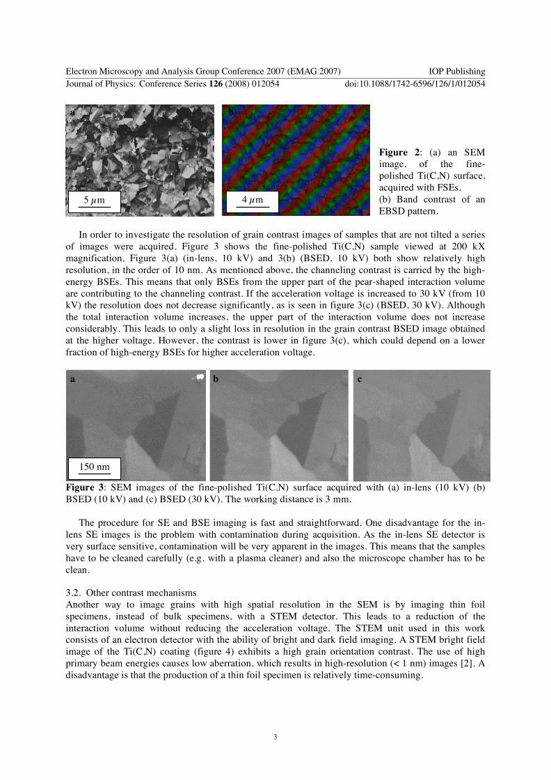
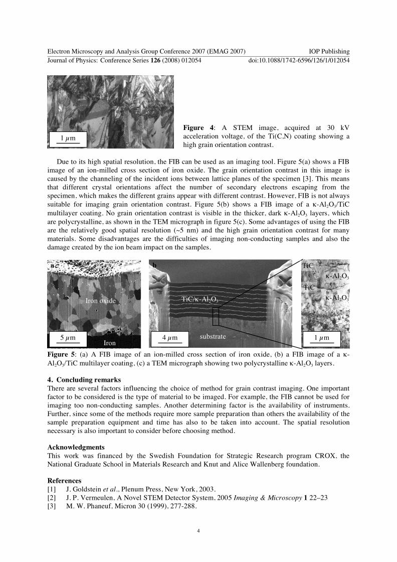