Embed Size (px)
Citation preview
Journal of Crystal Growth 370 (2013) 191–196
Contents lists available at SciVerse ScienceDirect
Journal of Crystal Growth
0022-02
http://d
n Corr
E-m1 Pr
German
journal homepage: www.elsevier.com/locate/jcrysgro
Growth of (BGa)As, (BGa)P, (BGa)(AsP) and (BGaIn)P by MOVPE
N. Sommer, R. Buss, J. Ohlmann, T. Wegele, C. Jurecka, S. Liebich, B. Kunert 1,W. Stolz, K. Volz n
Materials Science Center and Faculty of Physics, Philipps-Universitat, Hans Meerwein St., D-35032 Marburg, Germany
a r t i c l e i n f o
Available online 28 July 2012
Keywords:
A3. Metal organic vapour phase epitaxy
B2. Semiconducting III/V systems
B2. Semiconducting dilute boride III/V
systems
48/$ - see front matter & 2012 Elsevier B.V. A
x.doi.org/10.1016/j.jcrysgro.2012.07.035
esponding author. Tel.: þ49 6421 2822297.
ail address: [email protected]
esent address: NAsP III/V GmbH, Am Kn
y.
a b s t r a c t
The boron containing III/V-semiconductors (BGa)As, (BGa)P, (BGa)(AsP) and (BGaIn)P are grown by
metal–organic-vapour-phase-epitaxy. The influence of growth conditions on maximum boron incor-
poration, boron incorporation efficiency and structural quality is investigated.
A maximum boron concentration of 7.8% for (BGa)P and 9.9% for (BGa)(AsP) can be realized. Low
growth temperature of 525 1C and high V/III-ratios are needed to increase the maximum boron
concentration and to improve the structural quality.
A difference in boron incorporation efficiency and maximum boron concentration between (BGa)As
and (BGa)P is observed. The TBAs/V ratio in the gas phase is identified as the factor determining the
boron incorporation efficiency in (BGa)(AsP). (BGaIn)P samples with an indium concentration of 53%
and a maximum boron concentration of 4% are realized.
The possibility to achieve boron concentrations of several percent in III/V-semiconductors offers
new perspectives for strain engineering in devices like multi-junction solar cells or semiconductor
lasers.
& 2012 Elsevier B.V. All rights reserved.
1. Introduction
Due to the small covalent radius of the boron atom, diluteboron containing semiconductors are interesting both from afundamental point of view and for strain engineering in newsemiconductor devices like multi-junction solar cells or lasers.
The novel Ga(NAsP)/(BGa)(AsP)/(BGa)P material system latticematched to Si substrate is a promising approach for a realmonolithic integration of III/V-based optoelectronics on Si-basedmicroelectronics [1–3]. A good understanding of the (BGa)(AsP)and (BGa)P barrier materials is essential to improve the perfor-mance of the laser. Boron containing III–V-semiconductors arealso potential candidates for high-concentration solar cells [4,5].
Arsenic based semiconductors like (BGa)As and (BGaIn)Ashave been intensively investigated [4–17]. Using TEB, TEGa andarsine as precursors Geisz et al. were able to achieve a boronconcentration of up to 7% in GaAs [6]. Saidi et al. also report onMOVPE grown (BGa)As with a boron concentration r7% [7].Groenert et al. have incorporated up to 7.8% boron in GaAs bymolecular beam epitaxy [8]. Gottschalch et al. grew (BGa)As with
ll rights reserved.
.de (K. Volz).
echtacker, 35041 Marburg,
a maximum boron concentration of 4% and (BGaIn)As latticematched to GaAs with B¼3% and In¼6% [9].
In contrast to the arsenic based materials, less is known forphosphorus based semiconductors like (BGa)P or (BGaIn)P[2,18–21]. (BGa)P with boron concentrations of up to 4% grownby MOVPE was reported by Gottschalch et al. [18]. Theoretical,but no experimental investigations exist about (BGaIn)P [19,20].
In this study, we investigate the phosphorus based materials(BGa)P and (BGaIn)P. We compare the properties of (BGa)As and(BGa)P and discuss the quaternary system (BGa)(AsP). The influenceof growth temperature, V/III-ratio, the V/V-ratio, the growth rate andthe chemical composition on boron incorporation is studied.
2. Experimental procedure
All samples were grown on GaP, GaAs and Si (001) substrates,respectively, depending on the intended crystal composition in acommercially available horizontal Aixtron AIX200-GFR reactorsystem at a standard reactor pressure of 50 mbar. Pd-purified H2
was used as the carrier gas. The substrate temperature was variedbetween 575 1C and 475 1C. The temperature was calibrated usingthe Al/Si eutectic formation at 577 1C. Tertiarybutyl arsine (TBAs)and tertiarybutyl phosphine (TBP) were used as group V pre-cursors. Triethylboron (TEB), triethylgallium (TEGa) and trimety-lindium (TMIn) were chosen as boron, gallium and indium
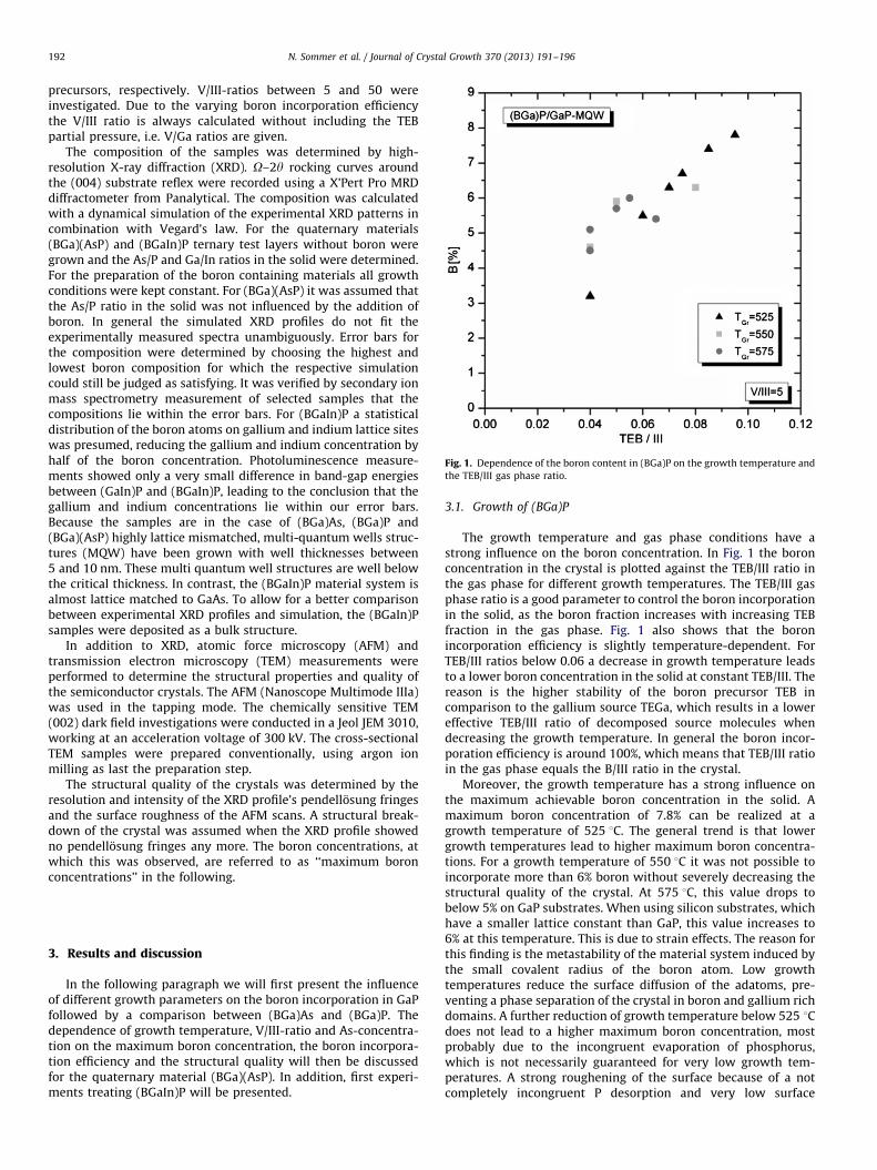
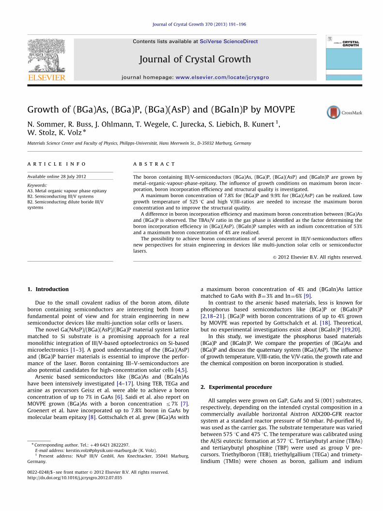
Fig. 1. Dependence of the boron content in (BGa)P on the growth temperature and
the TEB/III gas phase ratio.
N. Sommer et al. / Journal of Crystal Growth 370 (2013) 191–196192
precursors, respectively. V/III-ratios between 5 and 50 wereinvestigated. Due to the varying boron incorporation efficiencythe V/III ratio is always calculated without including the TEBpartial pressure, i.e. V/Ga ratios are given.
The composition of the samples was determined by high-resolution X-ray diffraction (XRD). O–2y rocking curves aroundthe (004) substrate reflex were recorded using a X’Pert Pro MRDdiffractometer from Panalytical. The composition was calculatedwith a dynamical simulation of the experimental XRD patterns incombination with Vegard’s law. For the quaternary materials(BGa)(AsP) and (BGaIn)P ternary test layers without boron weregrown and the As/P and Ga/In ratios in the solid were determined.For the preparation of the boron containing materials all growthconditions were kept constant. For (BGa)(AsP) it was assumed thatthe As/P ratio in the solid was not influenced by the addition ofboron. In general the simulated XRD profiles do not fit theexperimentally measured spectra unambiguously. Error bars forthe composition were determined by choosing the highest andlowest boron composition for which the respective simulationcould still be judged as satisfying. It was verified by secondary ionmass spectrometry measurement of selected samples that thecompositions lie within the error bars. For (BGaIn)P a statisticaldistribution of the boron atoms on gallium and indium lattice siteswas presumed, reducing the gallium and indium concentration byhalf of the boron concentration. Photoluminescence measure-ments showed only a very small difference in band-gap energiesbetween (GaIn)P and (BGaIn)P, leading to the conclusion that thegallium and indium concentrations lie within our error bars.Because the samples are in the case of (BGa)As, (BGa)P and(BGa)(AsP) highly lattice mismatched, multi-quantum wells struc-tures (MQW) have been grown with well thicknesses between5 and 10 nm. These multi quantum well structures are well belowthe critical thickness. In contrast, the (BGaIn)P material system isalmost lattice matched to GaAs. To allow for a better comparisonbetween experimental XRD profiles and simulation, the (BGaIn)Psamples were deposited as a bulk structure.
In addition to XRD, atomic force microscopy (AFM) andtransmission electron microscopy (TEM) measurements wereperformed to determine the structural properties and quality ofthe semiconductor crystals. The AFM (Nanoscope Multimode IIIa)was used in the tapping mode. The chemically sensitive TEM(002) dark field investigations were conducted in a Jeol JEM 3010,working at an acceleration voltage of 300 kV. The cross-sectionalTEM samples were prepared conventionally, using argon ionmilling as last the preparation step.
The structural quality of the crystals was determined by theresolution and intensity of the XRD profile’s pendellosung fringesand the surface roughness of the AFM scans. A structural break-down of the crystal was assumed when the XRD profile showedno pendellosung fringes any more. The boron concentrations, atwhich this was observed, are referred to as ‘‘maximum boronconcentrations’’ in the following.
3. Results and discussion
In the following paragraph we will first present the influenceof different growth parameters on the boron incorporation in GaPfollowed by a comparison between (BGa)As and (BGa)P. Thedependence of growth temperature, V/III-ratio and As-concentra-tion on the maximum boron concentration, the boron incorpora-tion efficiency and the structural quality will then be discussedfor the quaternary material (BGa)(AsP). In addition, first experi-ments treating (BGaIn)P will be presented.
3.1. Growth of (BGa)P
The growth temperature and gas phase conditions have astrong influence on the boron concentration. In Fig. 1 the boronconcentration in the crystal is plotted against the TEB/III ratio inthe gas phase for different growth temperatures. The TEB/III gasphase ratio is a good parameter to control the boron incorporationin the solid, as the boron fraction increases with increasing TEBfraction in the gas phase. Fig. 1 also shows that the boronincorporation efficiency is slightly temperature-dependent. ForTEB/III ratios below 0.06 a decrease in growth temperature leadsto a lower boron concentration in the solid at constant TEB/III. Thereason is the higher stability of the boron precursor TEB incomparison to the gallium source TEGa, which results in a lowereffective TEB/III ratio of decomposed source molecules whendecreasing the growth temperature. In general the boron incor-poration efficiency is around 100%, which means that TEB/III ratioin the gas phase equals the B/III ratio in the crystal.
Moreover, the growth temperature has a strong influence onthe maximum achievable boron concentration in the solid. Amaximum boron concentration of 7.8% can be realized at agrowth temperature of 525 1C. The general trend is that lowergrowth temperatures lead to higher maximum boron concentra-tions. For a growth temperature of 550 1C it was not possible toincorporate more than 6% boron without severely decreasing thestructural quality of the crystal. At 575 1C, this value drops tobelow 5% on GaP substrates. When using silicon substrates, whichhave a smaller lattice constant than GaP, this value increases to6% at this temperature. This is due to strain effects. The reason forthis finding is the metastability of the material system induced bythe small covalent radius of the boron atom. Low growthtemperatures reduce the surface diffusion of the adatoms, pre-venting a phase separation of the crystal in boron and gallium richdomains. A further reduction of growth temperature below 525 1Cdoes not lead to a higher maximum boron concentration, mostprobably due to the incongruent evaporation of phosphorus,which is not necessarily guaranteed for very low growth tem-peratures. A strong roughening of the surface because of a notcompletely incongruent P desorption and very low surface
N. Sommer et al. / Journal of Crystal Growth 370 (2013) 191–196 193
diffusion of the atoms is the result. Besides phase separation intoboron and gallium rich domains in the bulk, the maximum boronconcentration could also be limited by the strong local latticedistortions induced by the small boron atoms. In a Zincblendestructure every group-III atom has 12 group-III atoms as secondnearest neighbours. Above a critical boron concentration of1/12¼8.3% every additional boron atom will sit next to anotherboron atom assuming a statistical distribution of the boron atoms.The strong local lattice distortions lead eventually to a globalbreakdown of the crystal structure around 8% boron, which inturn defines the maximum achievable boron content.
The V/III ratio has no significant influence on the maximumboron concentration. A small increase in boron incorporationefficiency is seen for higher V/III ratios (data not shown here).
Nevertheless high V/III ratios are important to improve thestructural quality. Fig. 2 shows the surface morphology of (BGa)P/GaP MQW structures capped with a GaP layer. The boronconcentrations of both samples are comparable and the growthtemperatures are identical. The sample grown with V/III¼5 has avery rough surface whereas a high V/III¼50 leads to a muchsmoother surface morphology. Thus a better structural quality ofthe (BGa)P crystal can be achieved by using high V/III ratios. Thisis supported by theoretical calculations of Jenichen et al. whopredicted that strongly P-rich conditions are necessary to incor-porate isolated boron atoms or nearest neighbours into GaP [19].
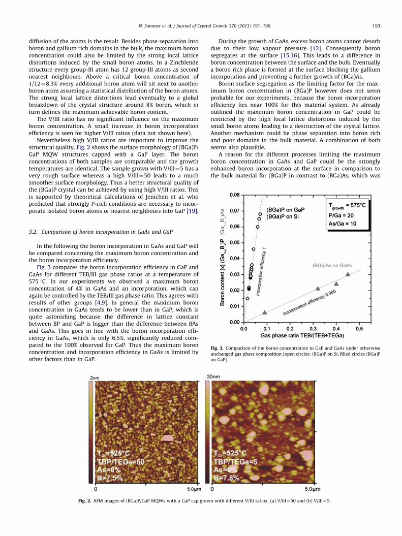
Fig. 3. Comparison of the boron concentration in GaP and GaAs under otherwise
unchanged gas phase composition (open circles: (BGa)P on Si, filled circles (BGa)P
on GaP).
3.2. Comparison of boron incorporation in GaAs and GaP
In the following the boron incorporation in GaAs and GaP willbe compared concerning the maximum boron concentration andthe boron incorporation efficiency.
Fig. 3 compares the boron incorporation efficiency in GaP andGaAs for different TEB/III gas phase ratios at a temperature of575 1C. In our experiments we observed a maximum boronconcentration of 4% in GaAs and an incorporation, which canagain be controlled by the TEB/III gas phase ratio. This agrees withresults of other groups [4,9]. In general the maximum boronconcentration in GaAs tends to be lower than in GaP, which isquite astonishing because the difference in lattice constantbetween BP and GaP is bigger than the difference between BAsand GaAs. This goes in line with the boron incorporation effi-ciency in GaAs, which is only 6.5%, significantly reduced com-pared to the 100% observed for GaP. Thus the maximum boronconcentration and incorporation efficiency in GaAs is limited byother factors than in GaP.
Fig. 2. AFM images of (BGa)P/GaP MQWs with a GaP cap grow
During the growth of GaAs, excess boron atoms cannot desorbdue to their low vapour pressure [12]. Consequently boronsegregates at the surface [15,16]. This leads to a difference inboron concentration between the surface and the bulk. Eventuallya boron rich phase is formed at the surface blocking the galliumincorporation and preventing a further growth of (BGa)As.
Boron surface segregation as the limiting factor for the max-imum boron concentration in (BGa)P however does not seemprobable for our experiments, because the boron incorporationefficiency lies near 100% for this material system. As alreadyoutlined the maximum boron concentration in GaP could berestricted by the high local lattice distortions induced by thesmall boron atoms leading to a destruction of the crystal lattice.Another mechanism could be phase separation into boron richand poor domains in the bulk material. A combination of bothseems also plausible.
A reason for the different processes limiting the maximumboron concentration in GaAs and GaP could be the stronglyenhanced boron incorporation at the surface in comparison tothe bulk material for (BGa)P in contrast to (BGa)As, which was
n with different V/III ratios: (a) V/III¼50 and (b) V/III¼5.
N. Sommer et al. / Journal of Crystal Growth 370 (2013) 191–196194
predicted through theoretical investigations by Jenichen andEngler [19]. This could explain the high boron incorporationefficiency in GaP in contrast to GaAs. In addition Jenichen et al.showed that boron antisite substitution in GaP unlike in GaAs isenergetically not favourable. This could be a reason for thestructural quality of (BGa)P being better than that of (BGa)Asfor the same boron concentration.
3.3. Growth of (BGa)(AsP)
The boron incorporation efficiency in the quaternary materialsystem (BGa)(AsP) decreases with increasing arsenic
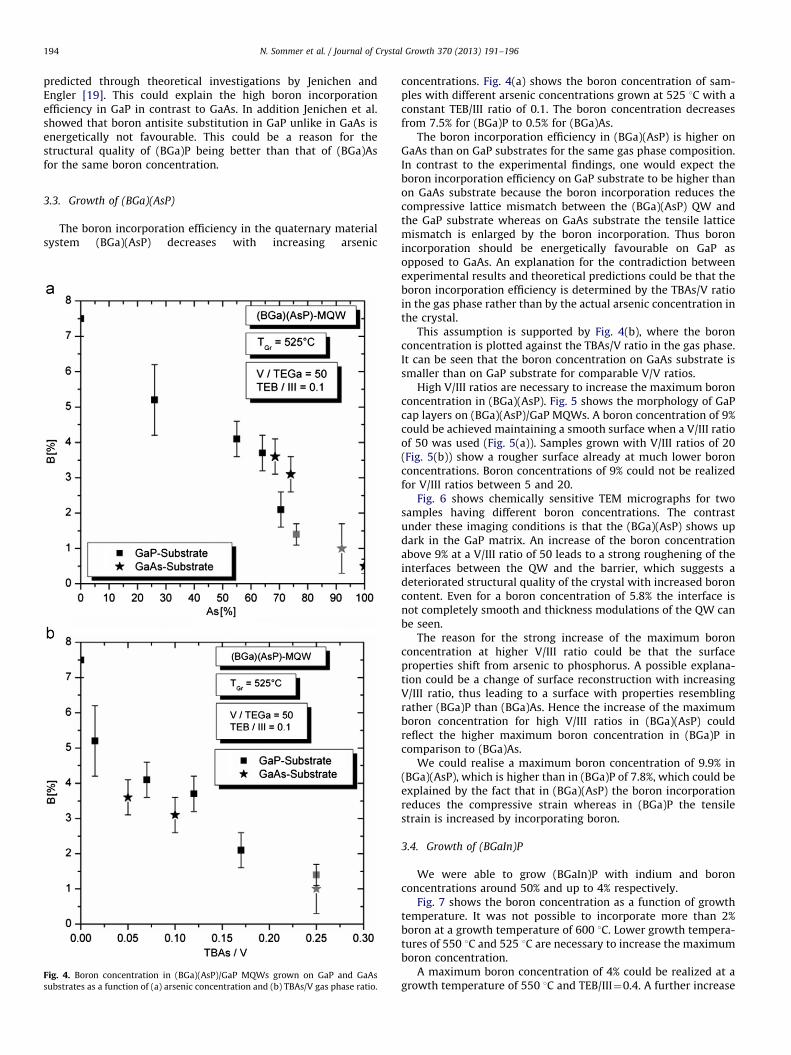
Fig. 4. Boron concentration in (BGa)(AsP)/GaP MQWs grown on GaP and GaAs
substrates as a function of (a) arsenic concentration and (b) TBAs/V gas phase ratio.
concentrations. Fig. 4(a) shows the boron concentration of sam-ples with different arsenic concentrations grown at 525 1C with aconstant TEB/III ratio of 0.1. The boron concentration decreasesfrom 7.5% for (BGa)P to 0.5% for (BGa)As.
The boron incorporation efficiency in (BGa)(AsP) is higher onGaAs than on GaP substrates for the same gas phase composition.In contrast to the experimental findings, one would expect theboron incorporation efficiency on GaP substrate to be higher thanon GaAs substrate because the boron incorporation reduces thecompressive lattice mismatch between the (BGa)(AsP) QW andthe GaP substrate whereas on GaAs substrate the tensile latticemismatch is enlarged by the boron incorporation. Thus boronincorporation should be energetically favourable on GaP asopposed to GaAs. An explanation for the contradiction betweenexperimental results and theoretical predictions could be that theboron incorporation efficiency is determined by the TBAs/V ratioin the gas phase rather than by the actual arsenic concentration inthe crystal.
This assumption is supported by Fig. 4(b), where the boronconcentration is plotted against the TBAs/V ratio in the gas phase.It can be seen that the boron concentration on GaAs substrate issmaller than on GaP substrate for comparable V/V ratios.
High V/III ratios are necessary to increase the maximum boronconcentration in (BGa)(AsP). Fig. 5 shows the morphology of GaPcap layers on (BGa)(AsP)/GaP MQWs. A boron concentration of 9%could be achieved maintaining a smooth surface when a V/III ratioof 50 was used (Fig. 5(a)). Samples grown with V/III ratios of 20(Fig. 5(b)) show a rougher surface already at much lower boronconcentrations. Boron concentrations of 9% could not be realizedfor V/III ratios between 5 and 20.
Fig. 6 shows chemically sensitive TEM micrographs for twosamples having different boron concentrations. The contrastunder these imaging conditions is that the (BGa)(AsP) shows updark in the GaP matrix. An increase of the boron concentrationabove 9% at a V/III ratio of 50 leads to a strong roughening of theinterfaces between the QW and the barrier, which suggests adeteriorated structural quality of the crystal with increased boroncontent. Even for a boron concentration of 5.8% the interface isnot completely smooth and thickness modulations of the QW canbe seen.
The reason for the strong increase of the maximum boronconcentration at higher V/III ratio could be that the surfaceproperties shift from arsenic to phosphorus. A possible explana-tion could be a change of surface reconstruction with increasingV/III ratio, thus leading to a surface with properties resemblingrather (BGa)P than (BGa)As. Hence the increase of the maximumboron concentration for high V/III ratios in (BGa)(AsP) couldreflect the higher maximum boron concentration in (BGa)P incomparison to (BGa)As.
We could realise a maximum boron concentration of 9.9% in(BGa)(AsP), which is higher than in (BGa)P of 7.8%, which could beexplained by the fact that in (BGa)(AsP) the boron incorporationreduces the compressive strain whereas in (BGa)P the tensilestrain is increased by incorporating boron.
3.4. Growth of (BGaIn)P
We were able to grow (BGaIn)P with indium and boronconcentrations around 50% and up to 4% respectively.
Fig. 7 shows the boron concentration as a function of growthtemperature. It was not possible to incorporate more than 2%boron at a growth temperature of 600 1C. Lower growth tempera-tures of 550 1C and 525 1C are necessary to increase the maximumboron concentration.
A maximum boron concentration of 4% could be realized at agrowth temperature of 550 1C and TEB/III¼0.4. A further increase
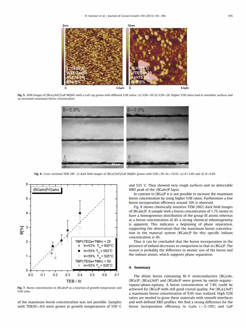
Fig. 5. AFM images of (BGa)(AsP)/GaP MQWs with a GaP cap grown with different V/III ratios: (a) V/III¼50 (b) V/III¼20. Higher V/III ratios lead to smoother surfaces and
an increased maximum boron concentration.
Fig. 6. Cross sectional TEM (00�2) dark field images of (BGa)(AsP)/GaP MQWs grown with V/III¼50, As¼74.5%: (a) B¼5.8% and (b) B¼9.9%.
Fig. 7. Boron concentration in (BGaIn)P as a function of growth temperature and
V/III ratio.
N. Sommer et al. / Journal of Crystal Growth 370 (2013) 191–196 195
of the maximum boron concentration was not possible. Sampleswith TEB/III¼0.6 were grown at growth temperatures of 550 1C
and 525 1C. They showed very rough surfaces and no detectableXRD peak of the (BGaIn)P layer.
In contrast to (BGa)P it is not possible to increase the maximumboron concentration by using higher V/III ratios. Furthermore a lowboron incorporation efficiency around 10% is observed.
Fig. 8 shows chemically sensitive TEM (002) dark field imagesof (BGaIn)P. A sample with a boron concentration of 1.7% seems tohave a homogeneous distribution of the group III atoms whereasat a boron concentration of 4% a strong chemical inhomogeneityis apparent. This indicates a beginning of phase separation,supporting the observation that the maximum boron concentra-tion in the material system (BGaIn)P for this specific indiumconcentration is 4%.
Thus it can be concluded that the boron incorporation in thepresence of indium decreases in comparison to that in (BGa)P. Thereason is probably the difference in atomic size of the boron andthe indium atoms, which supports phase separation.
4. Summary
The dilute boron containing III–V semiconductors (BGa)As,(BGa)P, (BGa)(AsP) and (BGaIn)P were grown by metal–organic-vapour-phase-epitaxy. A boron concentration of 7.8% could beachieved for (BGa)P with still good crystal quality. For (BGa)(AsP)a maximum boron concentration of 9.9% was realized. High V/IIIratios are needed to grow these materials with smooth interfacesand well defined XRD profiles. We find a strong difference for theboron incorporation efficiency in GaAs (�5–10%) and GaP
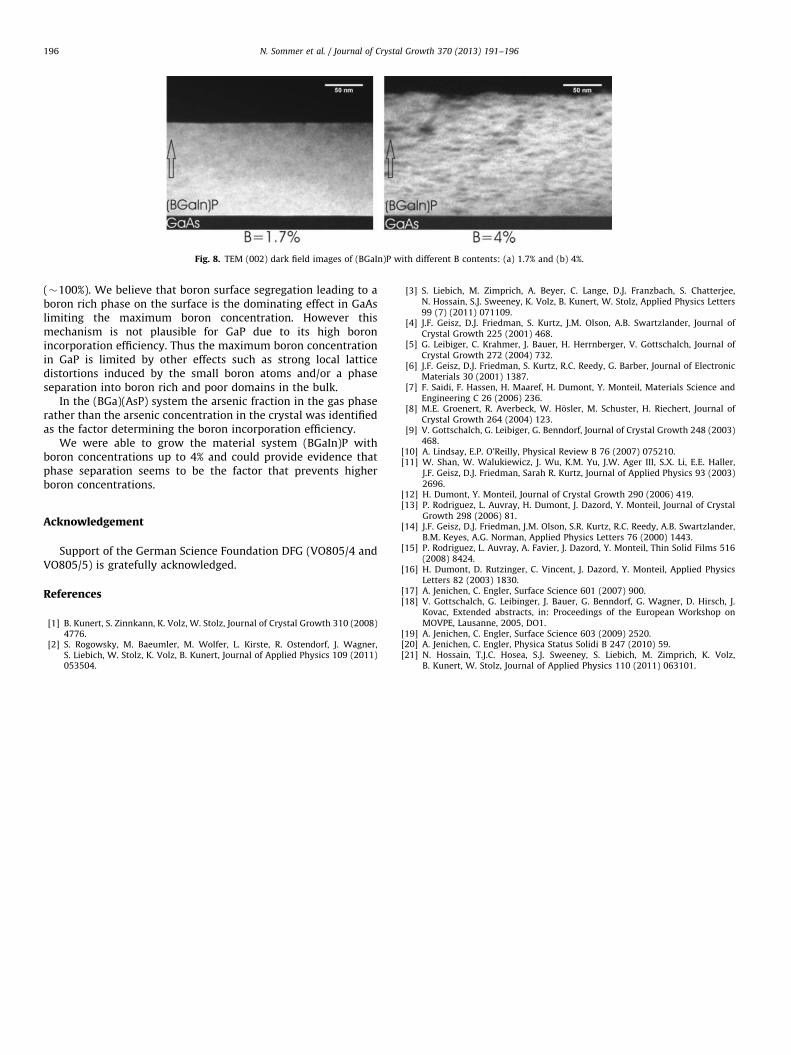
Fig. 8. TEM (002) dark field images of (BGaIn)P with different B contents: (a) 1.7% and (b) 4%.
N. Sommer et al. / Journal of Crystal Growth 370 (2013) 191–196196
(�100%). We believe that boron surface segregation leading to aboron rich phase on the surface is the dominating effect in GaAslimiting the maximum boron concentration. However thismechanism is not plausible for GaP due to its high boronincorporation efficiency. Thus the maximum boron concentrationin GaP is limited by other effects such as strong local latticedistortions induced by the small boron atoms and/or a phaseseparation into boron rich and poor domains in the bulk.
In the (BGa)(AsP) system the arsenic fraction in the gas phaserather than the arsenic concentration in the crystal was identifiedas the factor determining the boron incorporation efficiency.
We were able to grow the material system (BGaIn)P withboron concentrations up to 4% and could provide evidence thatphase separation seems to be the factor that prevents higherboron concentrations.
Acknowledgement
Support of the German Science Foundation DFG (VO805/4 andVO805/5) is gratefully acknowledged.
References
[1] B. Kunert, S. Zinnkann, K. Volz, W. Stolz, Journal of Crystal Growth 310 (2008)4776.
[2] S. Rogowsky, M. Baeumler, M. Wolfer, L. Kirste, R. Ostendorf, J. Wagner,S. Liebich, W. Stolz, K. Volz, B. Kunert, Journal of Applied Physics 109 (2011)053504.
[3] S. Liebich, M. Zimprich, A. Beyer, C. Lange, D.J. Franzbach, S. Chatterjee,N. Hossain, S.J. Sweeney, K. Volz, B. Kunert, W. Stolz, Applied Physics Letters99 (7) (2011) 071109.
[4] J.F. Geisz, D.J. Friedman, S. Kurtz, J.M. Olson, A.B. Swartzlander, Journal ofCrystal Growth 225 (2001) 468.
[5] G. Leibiger, C. Krahmer, J. Bauer, H. Herrnberger, V. Gottschalch, Journal ofCrystal Growth 272 (2004) 732.
[6] J.F. Geisz, D.J. Friedman, S. Kurtz, R.C. Reedy, G. Barber, Journal of ElectronicMaterials 30 (2001) 1387.
[7] F. Saidi, F. Hassen, H. Maaref, H. Dumont, Y. Monteil, Materials Science andEngineering C 26 (2006) 236.
[8] M.E. Groenert, R. Averbeck, W. Hosler, M. Schuster, H. Riechert, Journal ofCrystal Growth 264 (2004) 123.
[9] V. Gottschalch, G. Leibiger, G. Benndorf, Journal of Crystal Growth 248 (2003)468.
[10] A. Lindsay, E.P. O’Reilly, Physical Review B 76 (2007) 075210.[11] W. Shan, W. Walukiewicz, J. Wu, K.M. Yu, J.W. Ager III, S.X. Li, E.E. Haller,
J.F. Geisz, D.J. Friedman, Sarah R. Kurtz, Journal of Applied Physics 93 (2003)2696.
[12] H. Dumont, Y. Monteil, Journal of Crystal Growth 290 (2006) 419.[13] P. Rodriguez, L. Auvray, H. Dumont, J. Dazord, Y. Monteil, Journal of Crystal
Growth 298 (2006) 81.[14] J.F. Geisz, D.J. Friedman, J.M. Olson, S.R. Kurtz, R.C. Reedy, A.B. Swartzlander,
B.M. Keyes, A.G. Norman, Applied Physics Letters 76 (2000) 1443.[15] P. Rodriguez, L. Auvray, A. Favier, J. Dazord, Y. Monteil, Thin Solid Films 516
(2008) 8424.[16] H. Dumont, D. Rutzinger, C. Vincent, J. Dazord, Y. Monteil, Applied Physics
Letters 82 (2003) 1830.[17] A. Jenichen, C. Engler, Surface Science 601 (2007) 900.[18] V. Gottschalch, G. Leibinger, J. Bauer, G. Benndorf, G. Wagner, D. Hirsch, J.
Kovac, Extended abstracts, in: Proceedings of the European Workshop onMOVPE, Lausanne, 2005, DO1.
[19] A. Jenichen, C. Engler, Surface Science 603 (2009) 2520.[20] A. Jenichen, C. Engler, Physica Status Solidi B 247 (2010) 59.[21] N. Hossain, T.J.C. Hosea, S.J. Sweeney, S. Liebich, M. Zimprich, K. Volz,
B. Kunert, W. Stolz, Journal of Applied Physics 110 (2011) 063101.