Embed Size (px)
Citation preview
1
1
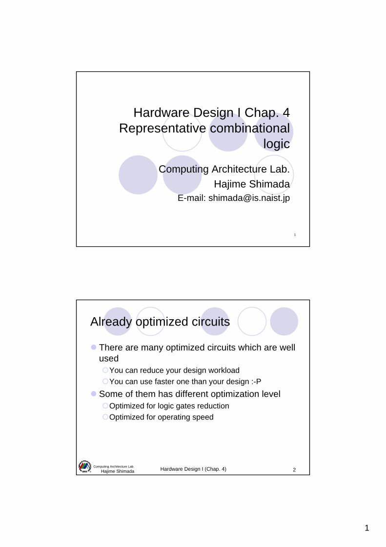
Hardware Design I Chap. 4Representative combinational
logic
Computing Architecture Lab.Hajime Shimada
E-mail: [email protected]
Hardware Design I (Chap. 4) 2Computing Architecture Lab.
Hajime Shimada
Already optimized circuits
There are many optimized circuits which are well used
You can reduce your design workloadYou can use faster one than your design :-P
Some of them has different optimization levelOptimized for logic gates reductionOptimized for operating speed
2
Hardware Design I (Chap. 4) 3Computing Architecture Lab.
Hajime Shimada
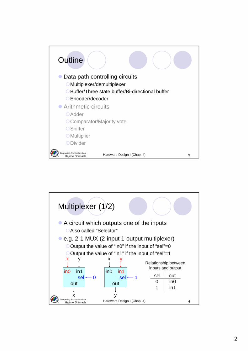
Outline
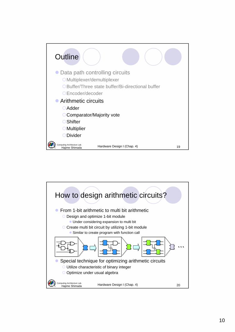
Data path controlling circuitsMultiplexer/demultiplexerBuffer/Three state buffer/Bi-directional bufferEncoder/decoder
Arithmetic circuitsAdder Comparator/Majority voteShifterMultiplierDivider
Hardware Design I (Chap. 4) 4Computing Architecture Lab.
Hajime Shimada
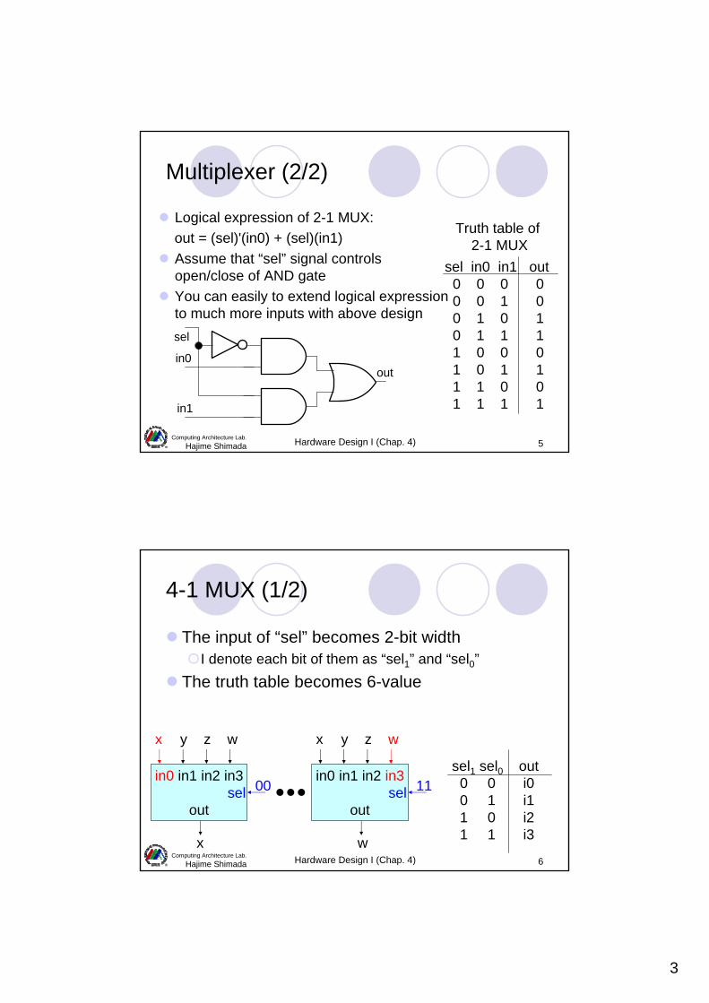
Multiplexer (1/2)
A circuit which outputs one of the inputsAlso called “Selector”
e.g. 2-1 MUX (2-input 1-output multiplexer)Output the value of “in0” if the input of “sel”=0Output the value of “in1” if the input of “sel”=1
in0 in1 sel
out
x y
x
0in0 in1
selout
x y
y
1 sel out0 in01 in1
Relationship betweeninputs and output
3
Hardware Design I (Chap. 4) 5Computing Architecture Lab.
Hajime Shimada
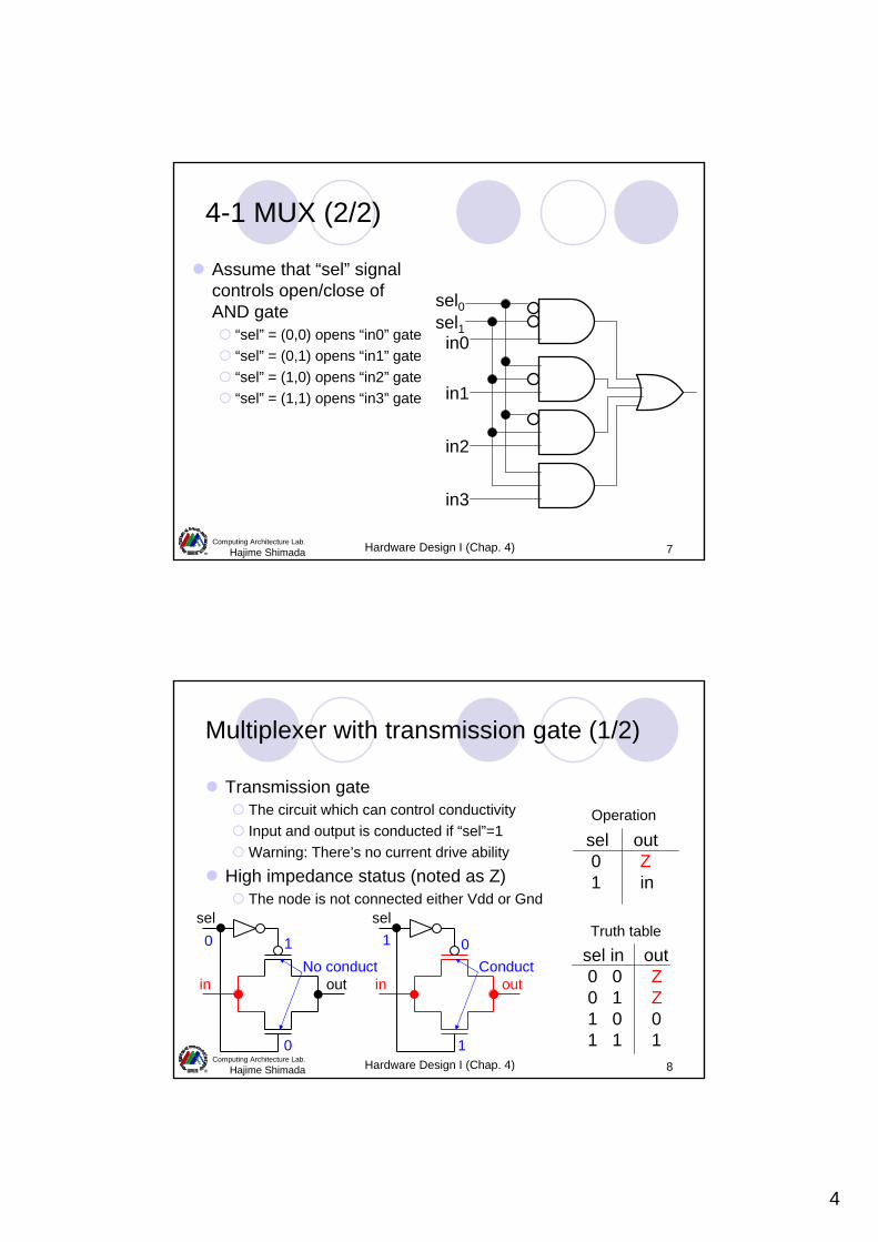
Multiplexer (2/2)
Logical expression of 2-1 MUX:out = (sel)'(in0) + (sel)(in1)Assume that “sel” signal controls open/close of AND gateYou can easily to extend logical expression to much more inputs with above design
sel in0 in1 out0 0 0 00 0 1 00 1 0 10 1 1 11 0 0 01 0 1 11 1 0 01 1 1 1
Truth table of 2-1 MUX
sel
in0
in1
out
Hardware Design I (Chap. 4) 6Computing Architecture Lab.
Hajime Shimada
4-1 MUX (1/2)
The input of “sel” becomes 2-bit widthI denote each bit of them as “sel1” and “sel0”
The truth table becomes 6-value
sel1 sel0 out0 0 i00 1 i11 0 i21 1 i3
in0 in1 in2 in3 sel
out
x y
x
00
z w
in0 in1 in2 in3sel
out
x y
w
11
z w
4
Hardware Design I (Chap. 4) 7Computing Architecture Lab.
Hajime Shimada
4-1 MUX (2/2)
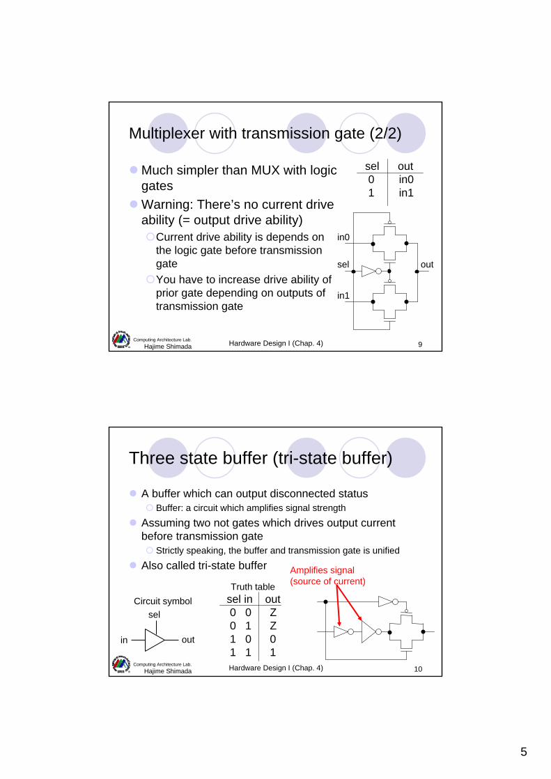
Assume that “sel” signal controls open/close of AND gate
“sel” = (0,0) opens “in0” gate“sel” = (0,1) opens “in1” gate“sel” = (1,0) opens “in2” gate“sel” = (1,1) opens “in3” gate
sel0sel1
in0
in1
in2
in3
Hardware Design I (Chap. 4) 8Computing Architecture Lab.
Hajime Shimada
Multiplexer with transmission gate (1/2)
Transmission gateThe circuit which can control conductivityInput and output is conducted if “sel”=1Warning: There’s no current drive ability
High impedance status (noted as Z)The node is not connected either Vdd or Gnd
in out
sel
sel out0 Z1 in
in out
sel0 11
10
0No conduct Conduct
sel in out0 0 Z0 1 Z1 0 01 1 1
Operation
Truth table
5
Hardware Design I (Chap. 4) 9Computing Architecture Lab.
Hajime Shimada
Multiplexer with transmission gate (2/2)
Much simpler than MUX with logic gatesWarning: There’s no current drive ability (= output drive ability)
Current drive ability is depends on the logic gate before transmission gateYou have to increase drive ability of prior gate depending on outputs of transmission gate
sel
in0
in1
sel out0 in01 in1
out
Hardware Design I (Chap. 4) 10Computing Architecture Lab.
Hajime Shimada
Three state buffer (tri-state buffer)
A buffer which can output disconnected statusBuffer: a circuit which amplifies signal strength
Assuming two not gates which drives output current before transmission gate
Strictly speaking, the buffer and transmission gate is unified
Also called tri-state buffer
sel in out0 0 Z0 1 Z1 0 01 1 1
in out
selCircuit symbol
Truth table
Amplifies signal(source of current)
6
Hardware Design I (Chap. 4) 11Computing Architecture Lab.
Hajime Shimada
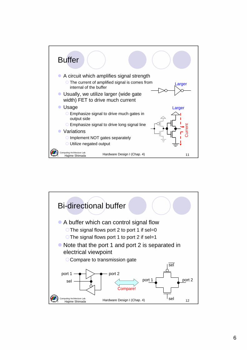
Buffer
A circuit which amplifies signal strengthThe current of amplified signal is comes from internal of the buffer
Usually, we utilize larger (wide gate width) FET to drive much currentUsage
Emphasize signal to drive much gates in output sideEmphasize signal to drive long signal line
VariationsImplement NOT gates separatelyUtilize negated output
Larger
Larger
Cur
rent
Hardware Design I (Chap. 4) 12Computing Architecture Lab.
Hajime Shimada
Bi-directional buffer
A buffer which can control signal flowThe signal flows port 2 to port 1 if sel=0The signal flows port 1 to port 2 if sel=1
Note that the port 1 and port 2 is separated in electrical viewpoint
Compare to transmission gate
port 2port 1
sel
Compare!
port 2port 1
sel
sel
7
Hardware Design I (Chap. 4) 13Computing Architecture Lab.
Hajime Shimada
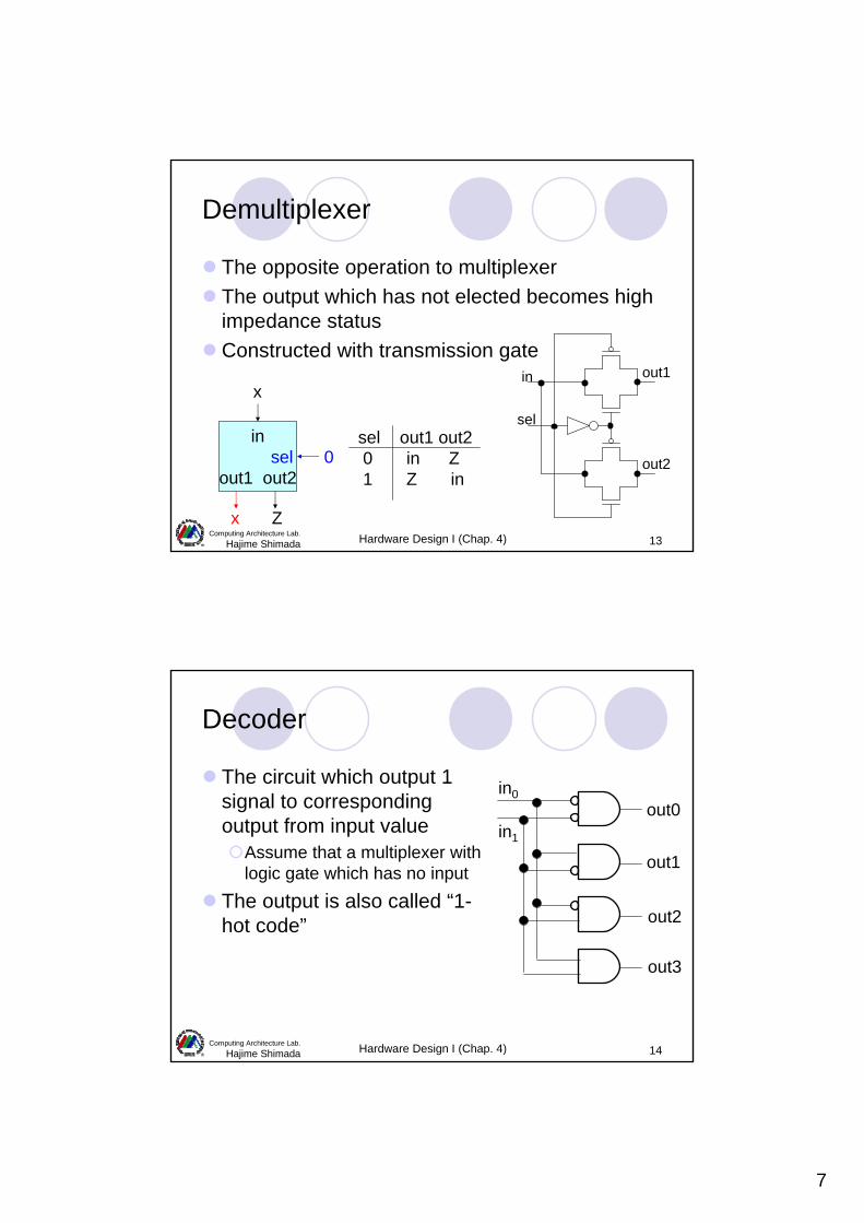
Demultiplexer
The opposite operation to multiplexerThe output which has not elected becomes high impedance statusConstructed with transmission gate
insel
out1 out2
x Z
x
0
sel
in
sel out1 out20 in Z1 Z in
out1
out2
Hardware Design I (Chap. 4) 14Computing Architecture Lab.
Hajime Shimada
Decoder
The circuit which output 1 signal to corresponding output from input value
Assume that a multiplexer with logic gate which has no input
The output is also called “1-hot code”
in0
in1
out0
out1
out2
out3
8
Hardware Design I (Chap. 4) 15Computing Architecture Lab.
Hajime Shimada
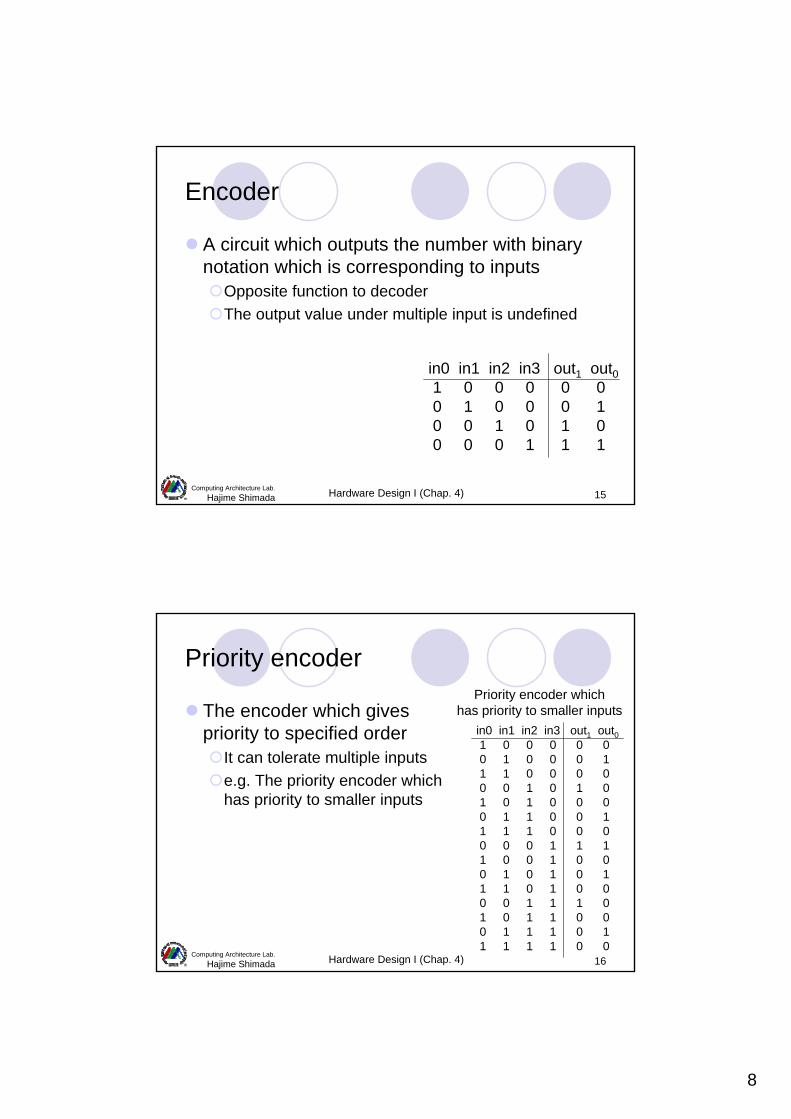
Encoder
A circuit which outputs the number with binary notation which is corresponding to inputs
Opposite function to decoderThe output value under multiple input is undefined
in0 in1 in2 in3 out1 out01 0 0 0 0 00 1 0 0 0 10 0 1 0 1 00 0 0 1 1 1
Hardware Design I (Chap. 4) 16Computing Architecture Lab.
Hajime Shimada
Priority encoder
The encoder which gives priority to specified order
It can tolerate multiple inputse.g. The priority encoder which has priority to smaller inputs
in0 in1 in2 in3 out1 out01 0 0 0 0 00 1 0 0 0 11 1 0 0 0 00 0 1 0 1 01 0 1 0 0 00 1 1 0 0 11 1 1 0 0 00 0 0 1 1 11 0 0 1 0 00 1 0 1 0 11 1 0 1 0 00 0 1 1 1 01 0 1 1 0 00 1 1 1 0 11 1 1 1 0 0
Priority encoder whichhas priority to smaller inputs
9
Hardware Design I (Chap. 4) 17Computing Architecture Lab.
Hajime Shimada
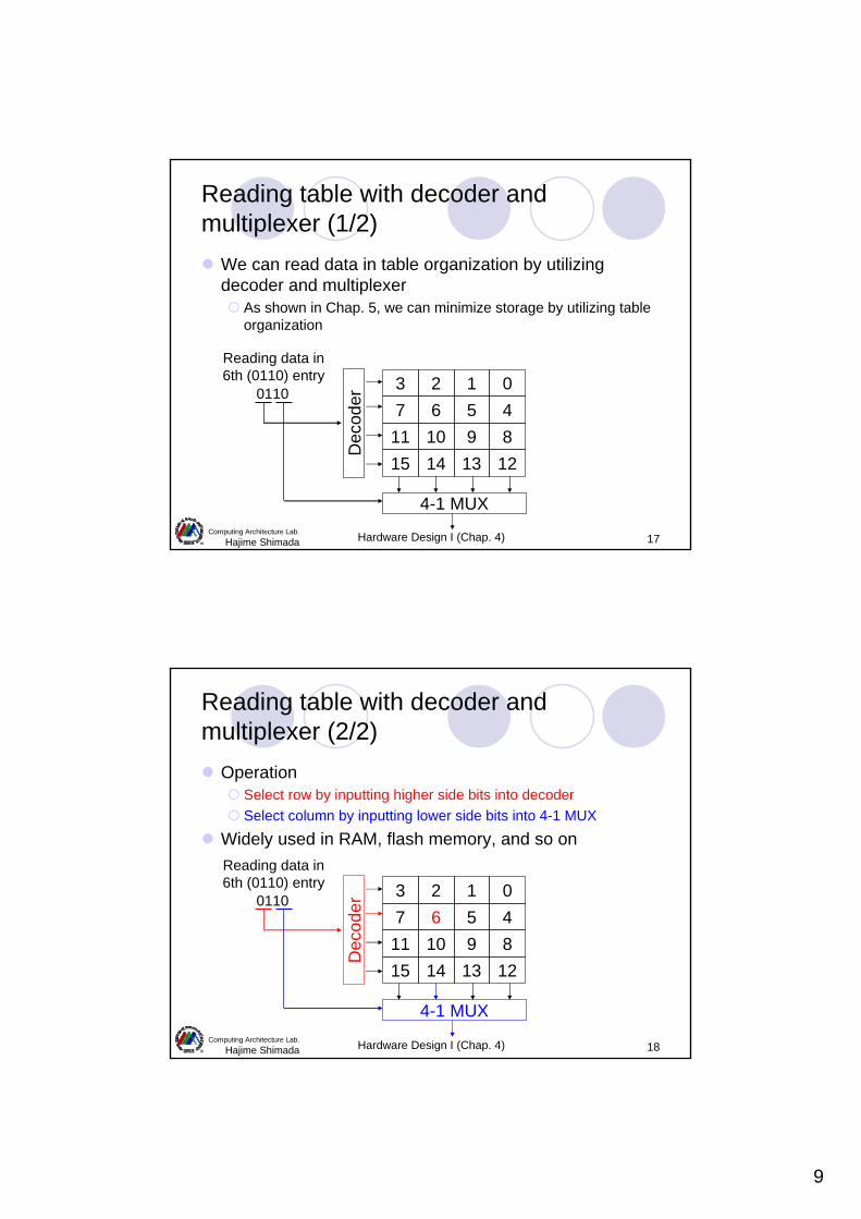
Reading table with decoder and multiplexer (1/2)
We can read data in table organization by utilizing decoder and multiplexer
As shown in Chap. 5, we can minimize storage by utilizing table organization
3 2 1 07 6 5 4
11 10 9 815 14 13 12
4-1 MUX
Reading data in6th (0110) entry
0110
Dec
oder
Hardware Design I (Chap. 4) 18Computing Architecture Lab.
Hajime Shimada
Reading table with decoder and multiplexer (2/2)
OperationSelect row by inputting higher side bits into decoderSelect column by inputting lower side bits into 4-1 MUX
Widely used in RAM, flash memory, and so on
3 2 1 07 6 5 4
11 10 9 815 14 13 12
4-1 MUX
Reading data in6th (0110) entry
0110
Dec
oder
10
Hardware Design I (Chap. 4) 19Computing Architecture Lab.
Hajime Shimada
Outline
Data path controlling circuitsMultiplexer/demultiplexerBuffer/Three state buffer/Bi-directional bufferEncoder/decoder
Arithmetic circuitsAdder Comparator/Majority voteShifterMultiplierDivider
Hardware Design I (Chap. 4) 20Computing Architecture Lab.
Hajime Shimada
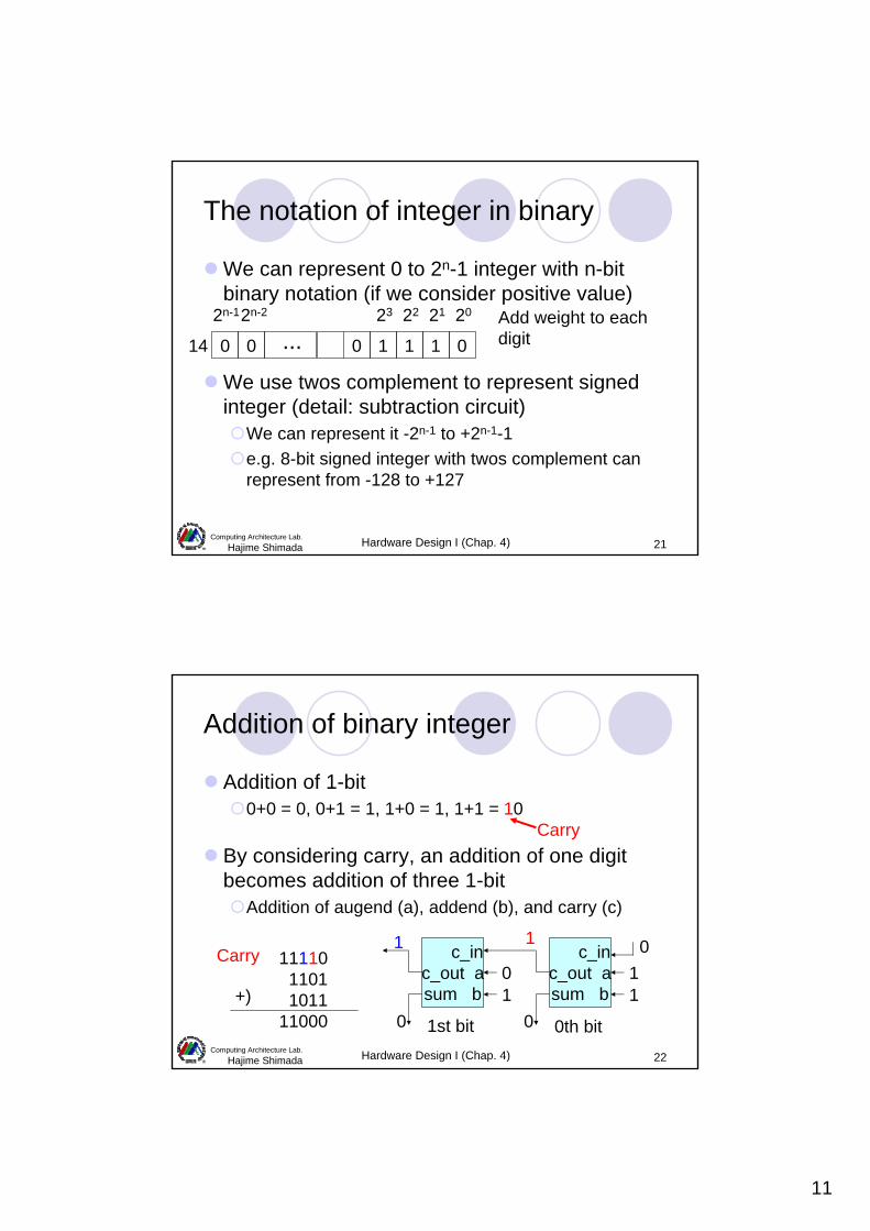
How to design arithmetic circuits?
From 1-bit arithmetic to multi bit arithmeticDesign and optimize 1-bit module
Under considering expansion to multi bitCreate multi bit circuit by utilizing 1-bit module
Similar to create program with function call
Special technique for optimizing arithmetic circuitsUtilize characteristic of binary integerOptimize under usual algebra
……
11
Hardware Design I (Chap. 4) 21Computing Architecture Lab.
Hajime Shimada
The notation of integer in binary
We can represent 0 to 2n-1 integer with n-bit binary notation (if we consider positive value)
We use twos complement to represent signed integer (detail: subtraction circuit)
We can represent it -2n-1 to +2n-1-1e.g. 8-bit signed integer with twos complement can represent from -128 to +127
0 0 0 1 1 1 0
202122232n-1 Add weight to eachdigit14 ...
2n-2
Hardware Design I (Chap. 4) 22Computing Architecture Lab.
Hajime Shimada
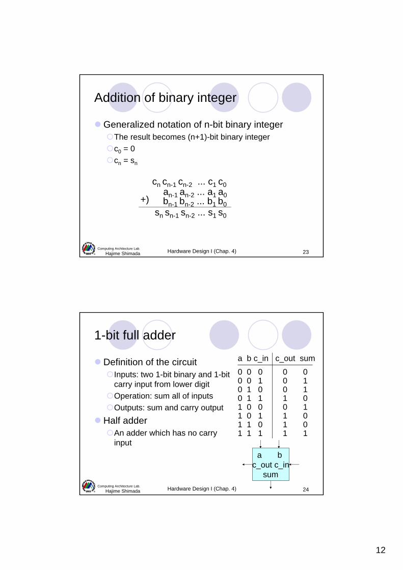
Addition of binary integer
Addition of 1-bit0+0 = 0, 0+1 = 1, 1+0 = 1, 1+1 = 10
By considering carry, an addition of one digit becomes addition of three 1-bit
Addition of augend (a), addend (b), and carry (c)
Carry
1111011011011
11000+)
Carry c_inc_out asum b
c_inc_out asum b
011
0
1
10
1
0 0th bit1st bit
12
Hardware Design I (Chap. 4) 23Computing Architecture Lab.
Hajime Shimada
Addition of binary integer
Generalized notation of n-bit binary integerThe result becomes (n+1)-bit binary integerc0 = 0cn = sn
+)
cn cn-1 cn-2 ... c1 c0an-1 an-2 ... a1 a0bn-1 bn-2 ... b1 b0
sn sn-1 sn-2 ... s1 s0
Hardware Design I (Chap. 4) 24Computing Architecture Lab.
Hajime Shimada
1-bit full adder
Definition of the circuitInputs: two 1-bit binary and 1-bit carry input from lower digitOperation: sum all of inputsOutputs: sum and carry output
Half adderAn adder which has no carry input
a b c_in c_out sum
0 0 0 0 00 0 1 0 10 1 0 0 10 1 1 1 01 0 0 0 11 0 1 1 01 1 0 1 01 1 1 1 1
a b c_out c_in
sum
13
Hardware Design I (Chap. 4) 25Computing Architecture Lab.
Hajime Shimada
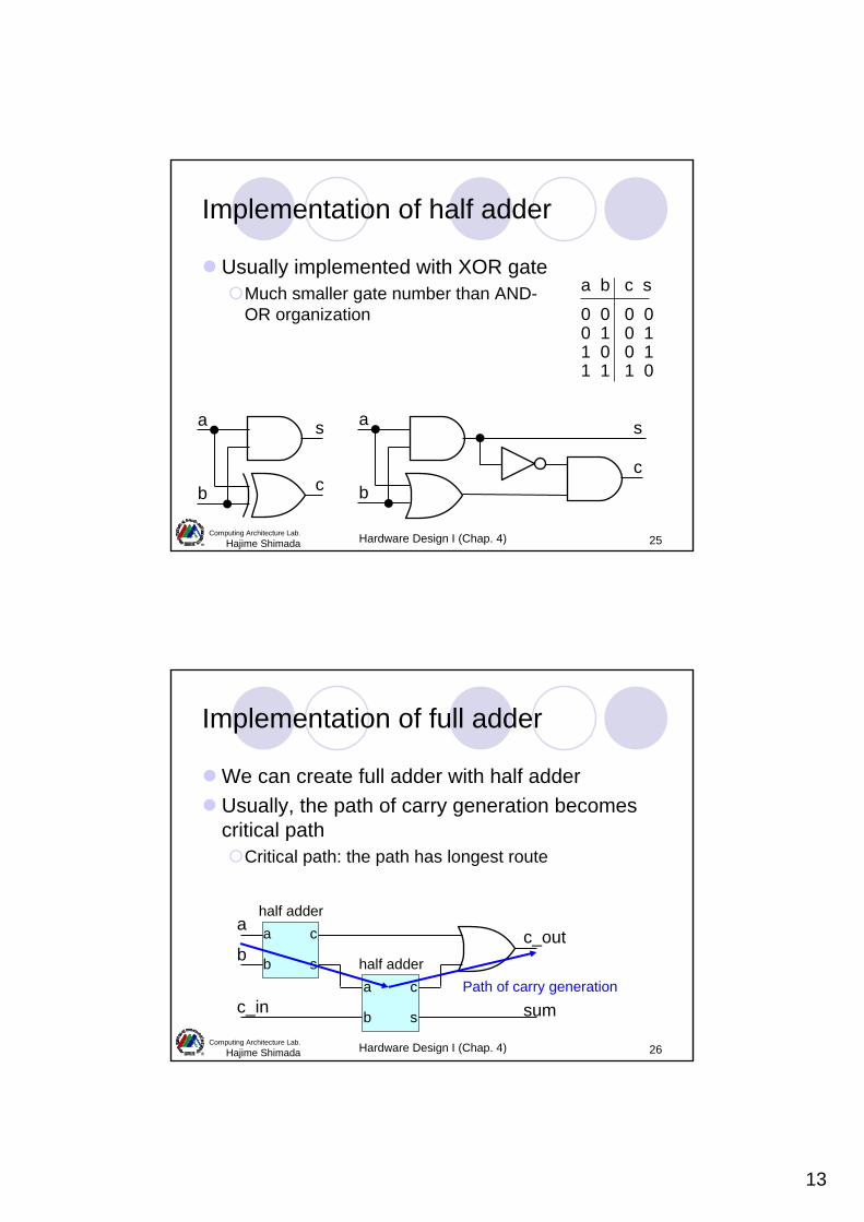
Implementation of half adder
Usually implemented with XOR gateMuch smaller gate number than AND-OR organization
a b c s
0 0 0 00 1 0 11 0 0 11 1 1 0
a
b
s
c
a
b
s
c
Hardware Design I (Chap. 4) 26Computing Architecture Lab.
Hajime Shimada
Implementation of full adder
We can create full adder with half adderUsually, the path of carry generation becomes critical path
Critical path: the path has longest route
a
b
c
s
half adder
a
b
c
s
half adder
a
bc_out
sumc_inPath of carry generation
14
Hardware Design I (Chap. 4) 27Computing Architecture Lab.
Hajime Shimada
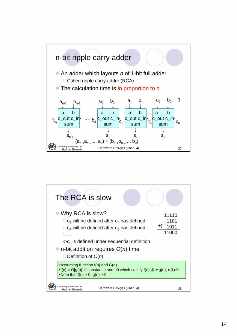
n-bit ripple carry adder
An adder which layouts n of 1-bit full adderCalled ripple carry adder (RCA)
The calculation time is in proportion to n
(an-1an-2 ... a0) + (bn-1bn-2 ... b0)
a b c_out c_in
sum
a b c_out c_in
sum
a b c_out c_in
sum
a b c_out c_in
sum
a0 b0a1 b1a2 b2an-1 bn-10
s0s1s2sn-1
c1c2c3cn
...c0
Hardware Design I (Chap. 4) 28Computing Architecture Lab.
Hajime Shimada
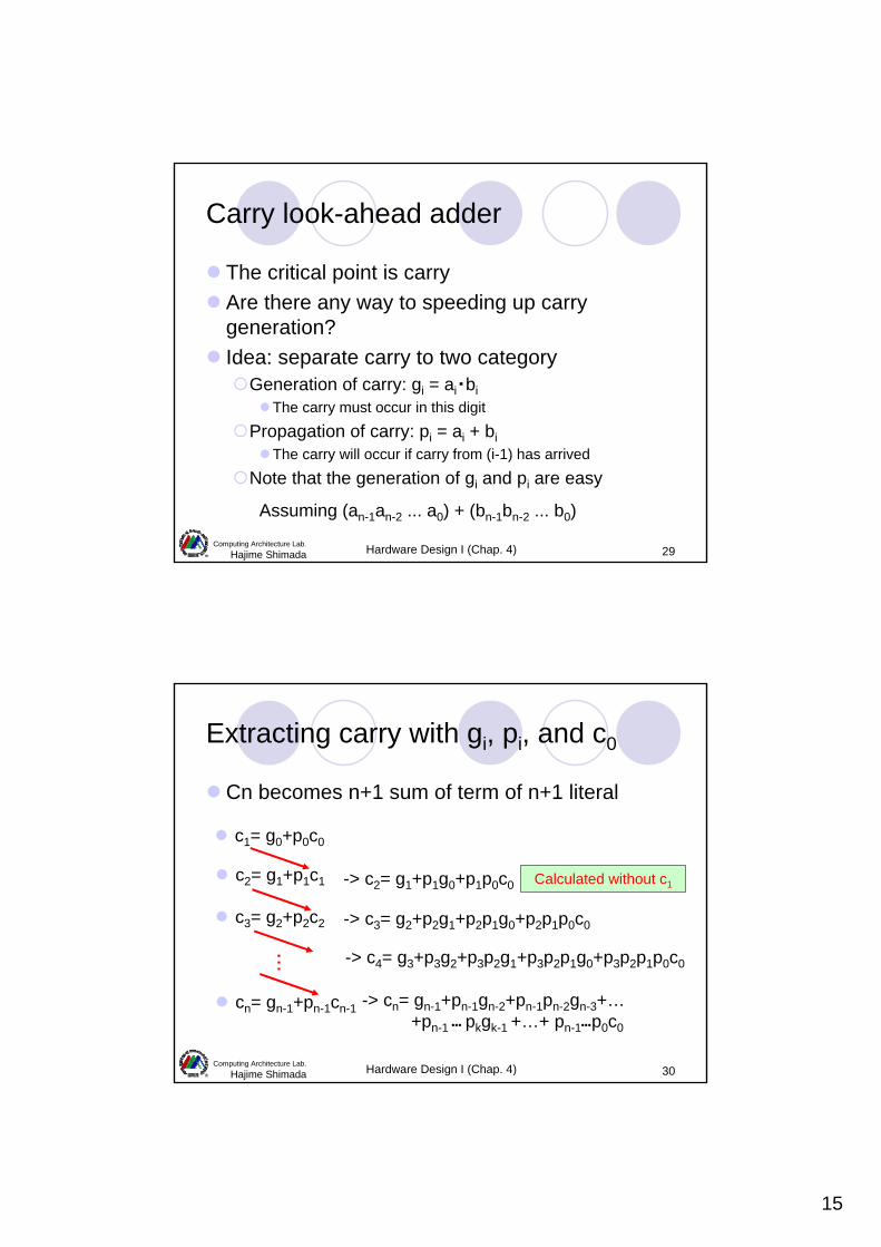
The RCA is slow
Why RCA is slow?c5 will be defined after c4 has definedc4 will be defined after c3 has defined...
->c5 is defined under sequential definitionn-bit addition requires O(n) time
Definition of O(n):
1111011011011
11000+)
•Assuming function f(n) and G(n)•f(n) = O[g(n)] if constant c and n0 which satisfy f(n) ≦c・g(n), n≧n0 •Note that f(n) > 0, g(n) > 0
15
Hardware Design I (Chap. 4) 29Computing Architecture Lab.
Hajime Shimada
Carry look-ahead adder
The critical point is carryAre there any way to speeding up carry generation? Idea: separate carry to two category
Generation of carry: gi = ai・biThe carry must occur in this digit
Propagation of carry: pi = ai + biThe carry will occur if carry from (i-1) has arrived
Note that the generation of gi and pi are easy
Assuming (an-1an-2 ... a0) + (bn-1bn-2 ... b0)
Hardware Design I (Chap. 4) 30Computing Architecture Lab.
Hajime Shimada
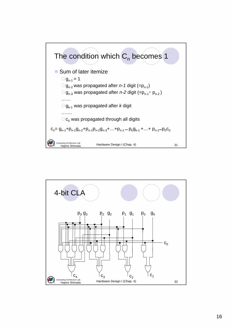
Extracting carry with gi, pi, and c0
Cn becomes n+1 sum of term of n+1 literal
c1= g0+p0c0
c2= g1+p1c1
c3= g2+p2c2
cn= gn-1+pn-1cn-1
-> c2= g1+p1g0+p1p0c0
-> c3= g2+p2g1+p2p1g0+p2p1p0c0
-> c4= g3+p3g2+p3p2g1+p3p2p1g0+p3p2p1p0c0...
-> cn= gn-1+pn-1gn-2+pn-1pn-2gn-3+…+pn-1 ••• pkgk-1 +…+ pn-1•••p0c0
Calculated without c1
16
Hardware Design I (Chap. 4) 31Computing Architecture Lab.
Hajime Shimada
The condition which Cn becomes 1
Sum of later itemizegn-1 = 1gn-2 was propagated after n-1 digit (=pn-1)gn-3 was propagated after n-2 digit (=pn-1・ pn-2 )
……gk-1 was propagated after k digit
…….c0 was propagated through all digits
cn= gn-1+pn-1gn-2+pn-1pn-2gn-3+…+pn-1 ••• pkgk-1 +…+ pn-1•••p0c0
Hardware Design I (Chap. 4) 32Computing Architecture Lab.
Hajime Shimada
4-bit CLA
g3p3 g2 g1
c0
g0 p2 p1 p0
c1 c2 c3 c4

17
Hardware Design I (Chap. 4) 33Computing Architecture Lab.
Hajime Shimada
The characteristic of CLA
It can calculate ci in parallelMuch complicated than RCACalculation time becomes O(log n)
cn becomes sum of n+1 termEach term is consist of n+1 literals
-> If we implement it with balance tree, the height becomes log n
Hardware Design I (Chap. 4) 34Computing Architecture Lab.
Hajime Shimada
Quiz
How long does CLA requires to calculate 64-bit value with NAND2 gate delay?1. Around 8 NAND2 gate delay2. Around 12 NAND2 gate delay3. Around 16 NAND2 gate delay4. Around 20 NAND2 gate delay
64-bit RCA requires around 129 NAND2 gate delay
18
Hardware Design I (Chap. 4) 35Computing Architecture Lab.
Hajime Shimada
Answer
2. Around 12 NAND2 gate delay1 NAND2 delay for prepare pi and giAbout 8 NAND2 delay for prepare ci from pi and gi3 NAND2 delay for calculate si
Result of practical implementationAlpha 21264 processor utilizes 12 FO4 delay for each pipeline stageIt execute 64-bit arithmetic in 1 pipeline stage
pipeline stage ->Chap. 11
Hardware Design I (Chap. 4) 36Computing Architecture Lab.
Hajime Shimada
Explore of faster adder
Adder is one of the important circuit so that there’s many implementationsExamples
Carry select adderConditional sum adderCarry skip adderCarry bypass adderCarry complete adderDomino logic adder for Pentium 4
19
Hardware Design I (Chap. 4) 37Computing Architecture Lab.
Hajime Shimada
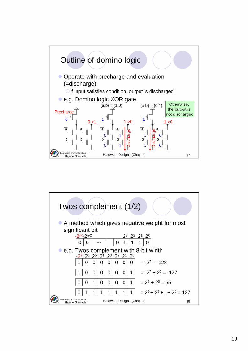
Outline of domino logic
Operate with precharge and evaluation (=discharge)
If input satisfies condition, output is dischargede.g. Domino logic XOR gate
Precharge
a
b
a
b
a
b
a
b
a
b
a
b0
0
0
0
1
1
1
1
(a,b) = (1,0) (a,b) = (0,1)
Dis
char
ge
Dis
char
ge
0->1 1->0 1->00 1 1
Otherwise, the output is
not discharged
Hardware Design I (Chap. 4) 38Computing Architecture Lab.
Hajime Shimada
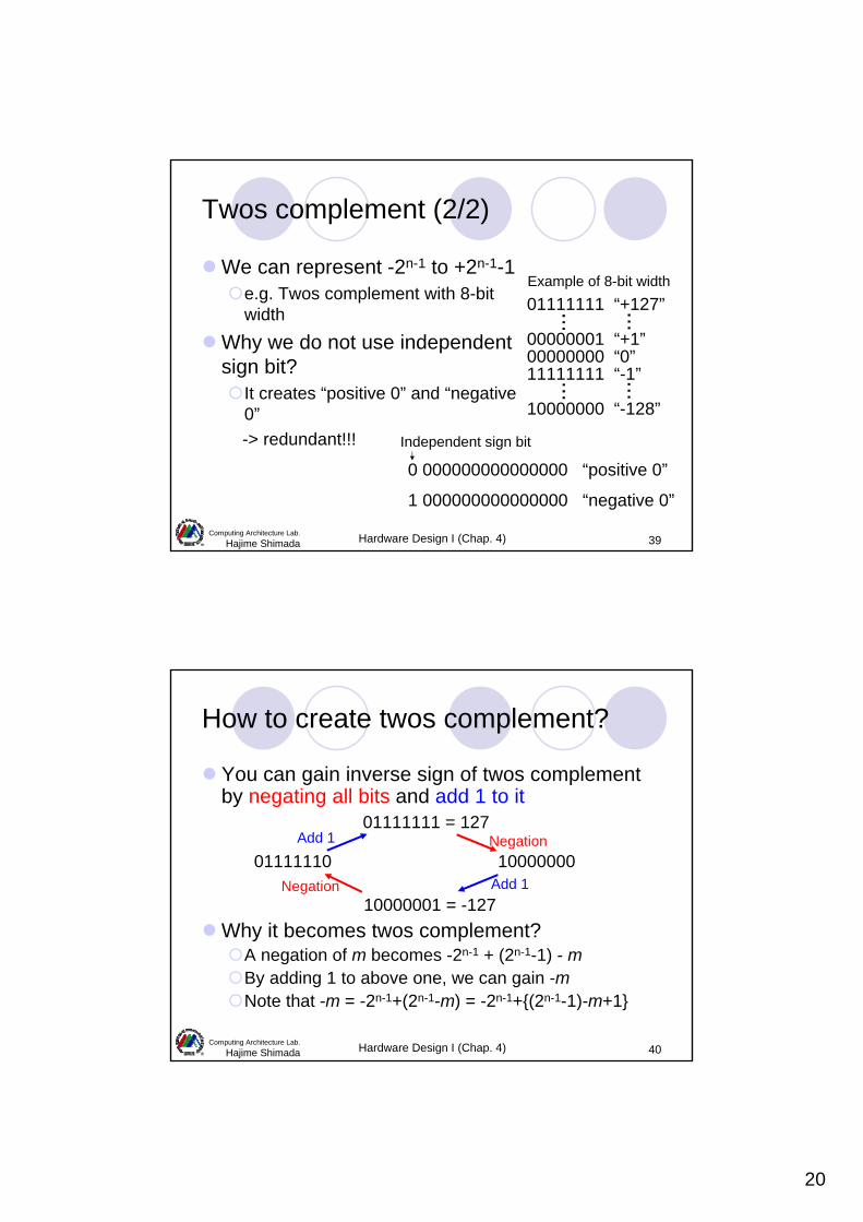
Twos complement (1/2)
A method which gives negative weight for most significant bit
e.g. Twos complement with 8-bit width0 0 0 1 1 1 0
20212223-2n-1
...2n-2
0 0 0 020212223
1 0 0 0242526-27
0 0 0 11 0 0 0
0 0 0 10 0 1 0
1 1 1 10 1 1 1
= -27 = -128
= -27 + 20 = -127
= 26 + 20 = 65
= 26 + 25 +...+ 20 = 127
20
Hardware Design I (Chap. 4) 39Computing Architecture Lab.
Hajime Shimada
Twos complement (2/2)
We can represent -2n-1 to +2n-1-1 e.g. Twos complement with 8-bit width
Why we do not use independent sign bit?
It creates “positive 0” and “negative 0”-> redundant!!!
0 000000000000000 “positive 0”
1 000000000000000 “negative 0”
Independent sign bit
00000001 “+1”00000000 “0”11111111 “-1”
10000000 “-128”
01111111 “+127”
......
......
Example of 8-bit width
Hardware Design I (Chap. 4) 40Computing Architecture Lab.
Hajime Shimada
How to create twos complement?
You can gain inverse sign of twos complement by negating all bits and add 1 to it
Why it becomes twos complement?A negation of m becomes -2n-1 + (2n-1-1) - mBy adding 1 to above one, we can gain -mNote that -m = -2n-1+(2n-1-m) = -2n-1+{(2n-1-1)-m+1}
Negation
Negation Add 1
Add 101111111 = 127
10000000
10000001 = -127
01111110
21
Hardware Design I (Chap. 4) 41Computing Architecture Lab.
Hajime Shimada
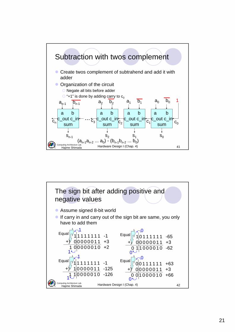
Subtraction with twos complement
Create twos complement of subtrahend and add it with adderOrganization of the circuit
Negate all bits before adder“+1” is done by adding carry to c0
(an-1an-2 ... a0) - (bn-1bn-2 ... b0)
a b c_out c_in
sum
a b c_out c_in
sum
a b c_out c_in
sum
a b c_out c_in
sum
a0 b0a1 b1a2 b2an-1 bn-11
s0s1s2sn-1
c1c2c3cn
...c0
Hardware Design I (Chap. 4) 42Computing Architecture Lab.
Hajime Shimada
The sign bit after adding positive and negative values
Assume signed 8-bit worldIf carry in and carry out of the sign bit are same, you only have to add them
1 1 1 1 1 1 1 10 0 0 0 0 0 1 10 0 0 0 0 0 1 0
+)-1+3+21
1 0 1 1 1 1 1 10 0 0 0 0 0 1 11 1 0 0 0 0 1 0
+)-65+3-62
1 1 1 1 1 1 1 11 0 0 0 0 0 1 11 0 0 0 0 0 1 0
+)-1-125-1261
0 0 1 1 1 1 1 10 0 0 0 0 0 1 10 1 0 0 0 0 1 0
+)+63+3+66
0
0
1 0
1 01 0
1 0
Equal Equal
EqualEqual
22
Hardware Design I (Chap. 4) 43Computing Architecture Lab.
Hajime Shimada
0
The sign bit after adding positive and negative values
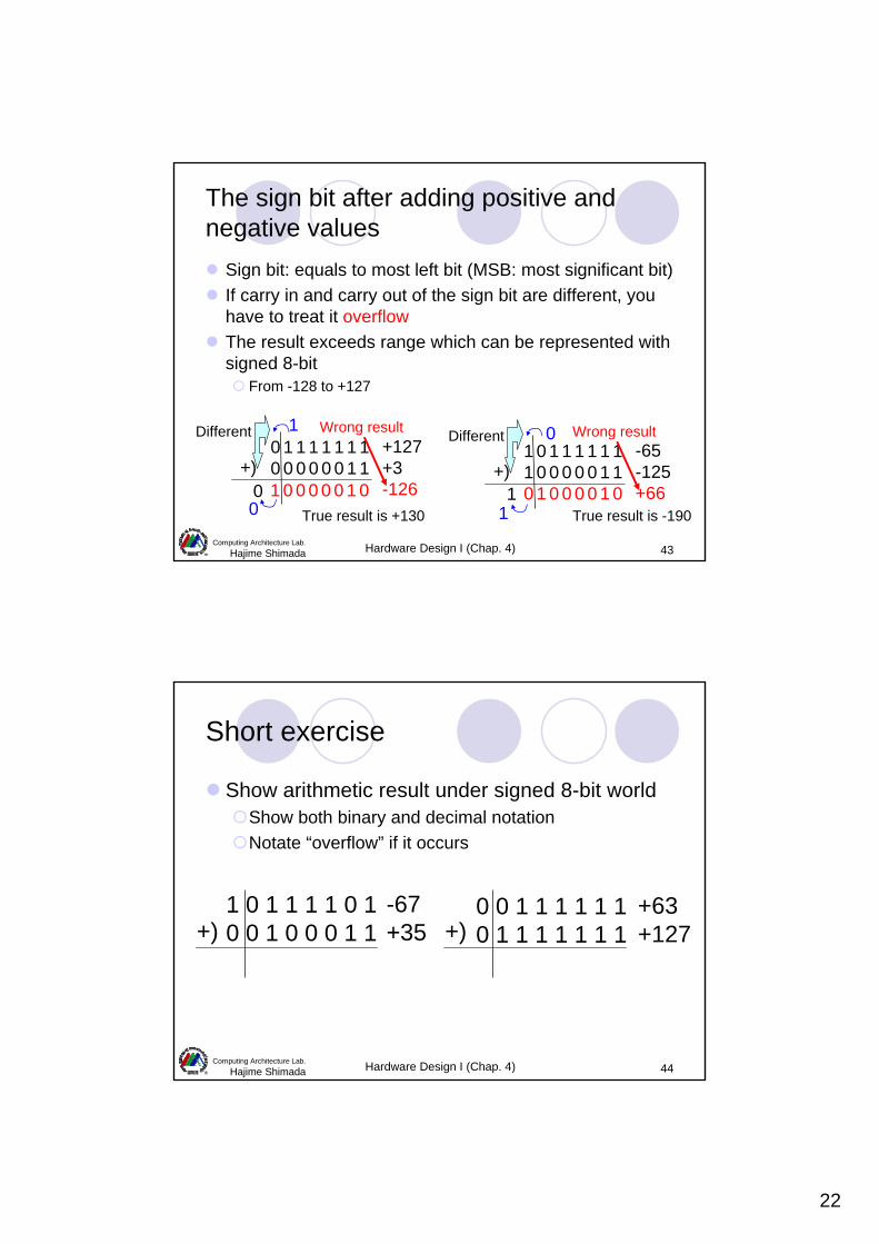
Sign bit: equals to most left bit (MSB: most significant bit)If carry in and carry out of the sign bit are different, you have to treat it overflowThe result exceeds range which can be represented with signed 8-bit
From -128 to +127
0 1 1 1 1 1 1 10 0 0 0 0 0 1 1+)
+127+3-126
11 0 1 1 1 1 1 11 0 0 0 0 0 1 10 1 0 0 0 0 1 0
+)-65-125+661
Wrong result0
0 1 0 0 0 0 0 1 0True result is +130 True result is -1901
DifferentDifferent Wrong result
Hardware Design I (Chap. 4) 44Computing Architecture Lab.
Hajime Shimada
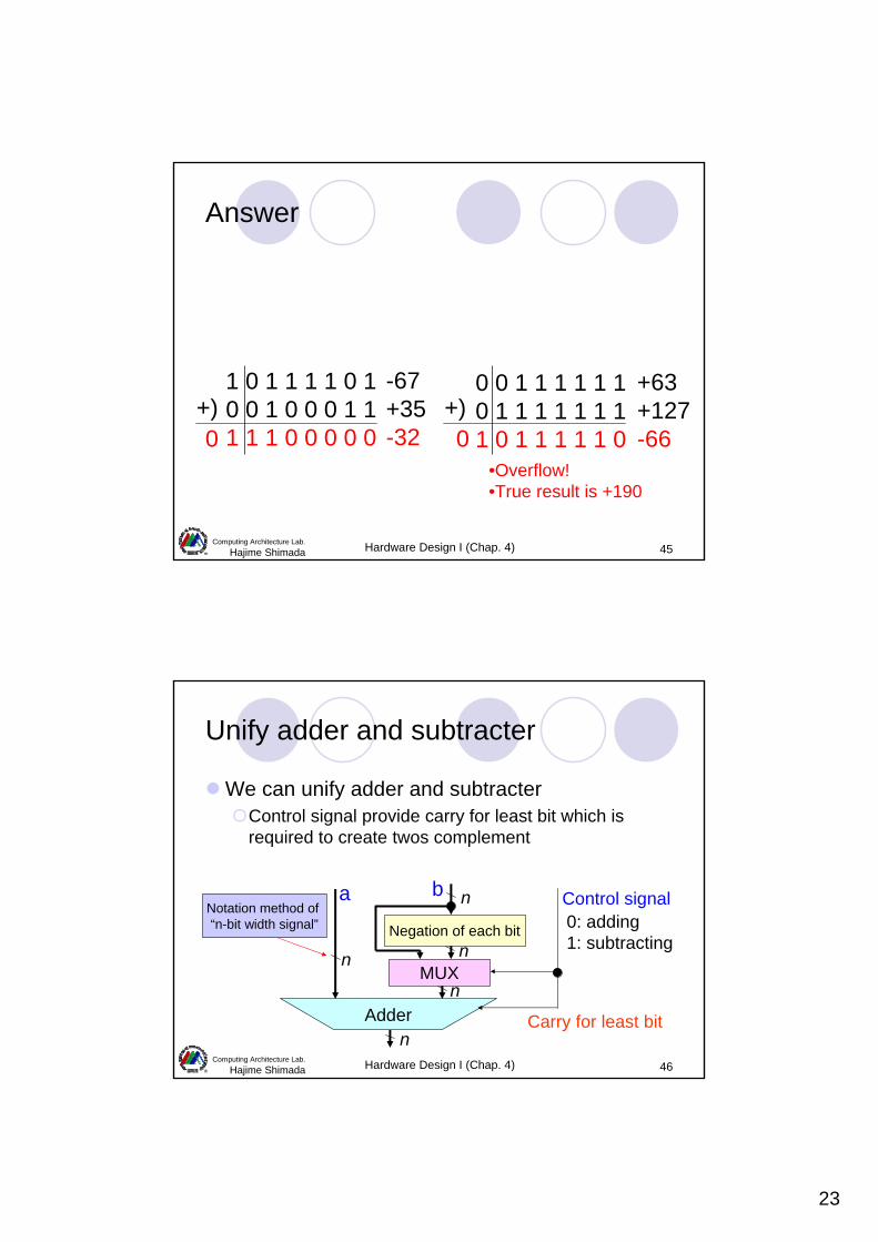
Short exercise
Show arithmetic result under signed 8-bit worldShow both binary and decimal notationNotate “overflow” if it occurs
1 0 1 1 1 1 0 10 0 1 0 0 0 1 1+)
-67 +35
0 0 1 1 1 1 1 10 1 1 1 1 1 1 1+)
+63+127
23
Hardware Design I (Chap. 4) 45Computing Architecture Lab.
Hajime Shimada
Answer
1 0 1 1 1 1 0 10 0 1 0 0 0 1 11 1 1 0 0 0 0 0
+)-67 +35-32
0 0 1 1 1 1 1 10 1 1 1 1 1 1 11 0 1 1 1 1 1 0
+)+63+127-660 0
•Overflow!•True result is +190
Hardware Design I (Chap. 4) 46Computing Architecture Lab.
Hajime Shimada
Unify adder and subtracter
We can unify adder and subtracterControl signal provide carry for least bit which is required to create twos complement
Negation of each bit
n
nMUX
n
n
n
Control signal
Carry for least bit
0: adding1: subtracting
a bNotation method of “n-bit width signal”
Adder

24
Hardware Design I (Chap. 4) 47Computing Architecture Lab.
Hajime Shimada
...
ALU (Arithmetic Logic Unit)
Usually, we implement multiple arithmetic function to one circuit We can share logic gates between arithmetics
e.g. AND/XOR operation of a and b are partial result of half adderWe can save number of logic gates
a b
Control(add, sub, compare,and, or, xor,...)
8 8
8
ALU
Hardware Design I (Chap. 4) 48Computing Architecture Lab.
Hajime Shimada
1-bit right shift
Movie 1 digit to rightLeast significant bit (LSB) is banishedMSB differs between shift method
Logical shift: insert 0Arithmetic shift: insert prior MSB
The result becomes divided by 2e.g. 00000111(+7) -> 00000011(+3)e.g. 11111010(-6) -> 11111101(-3)
Achieved with only wire connection
1 0 1 0 1 0 1 1
0 1 0 1 0 1 0 1
0
Logical shift:Arithmetic shift: 1 1 0 1 0 1 0 1
CopyInsert
25
Hardware Design I (Chap. 4) 49Computing Architecture Lab.
Hajime Shimada
1-bit left shift
Movie 1 digit to rightMSB is banished0 is inserted into LSB
The result becomes multiplied by 2e.g. 00000111(+7) -> 00001110(+14)e.g. 11111010(-6) -> 11110100(-12)
Also achieved with only wire connectionYou have to consider overflow if you execute arithmetic shift
e.g. 10000000(-128) -> 00000000(0) Overflow!
1 0 1 0 1 0 1 1
1 0 1 0 1 0 1 0
0Insert
Hardware Design I (Chap. 4) 50Computing Architecture Lab.
Hajime Shimada
1-bit rotate left (or right)
1-bit rotate leftMove 1 digit to leftMSB is moved to LSB
1-bit rotate rightMove 1 digit to rightLSB is moved to MSB
1 0 1 0 1 0 1 1
1 0 1 0 1 0 1 1
1 0 1 0 1 0 1 1
1 1 0 1 0 1 0 1
Rotate left
Rotate right
26
Hardware Design I (Chap. 4) 51Computing Architecture Lab.
Hajime Shimada
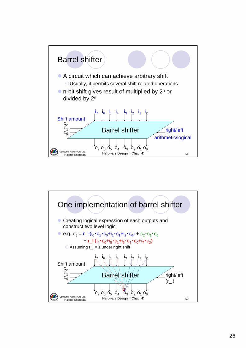
Barrel shifter
A circuit which can achieve arbitrary shiftUsually, it permits several shift related operations
n-bit shift gives result of multiplied by 2n or divided by 2n
Barrel shifter
i7 i6 i5 i4 i3 i2 i1 i0
o7 o6 o5 o4 o3 o2 o1 o0
c2c1c0right/left
arithmetic/logical
Shift amount
Hardware Design I (Chap. 4) 52Computing Architecture Lab.
Hajime Shimada
One implementation of barrel shifter
Creating logical expression of each outputs and construct two level logice.g. o3 = r_l’(i0・c1・c0+i1・c1+i2・c0) + c2・c1・c0
+ r_l (i4・c0+i5・c1+i6・c1・c0+i7・c2)Assuming r_l = 1 under right shift
Barrel shifter
i7 i6 i5 i4 i3 i2 i1 i0
o7 o6 o5 o4 o3 o2 o1 o0
c2c1c0right/left(r_l)
Shift amount
27
Hardware Design I (Chap. 4) 53Computing Architecture Lab.
Hajime Shimada
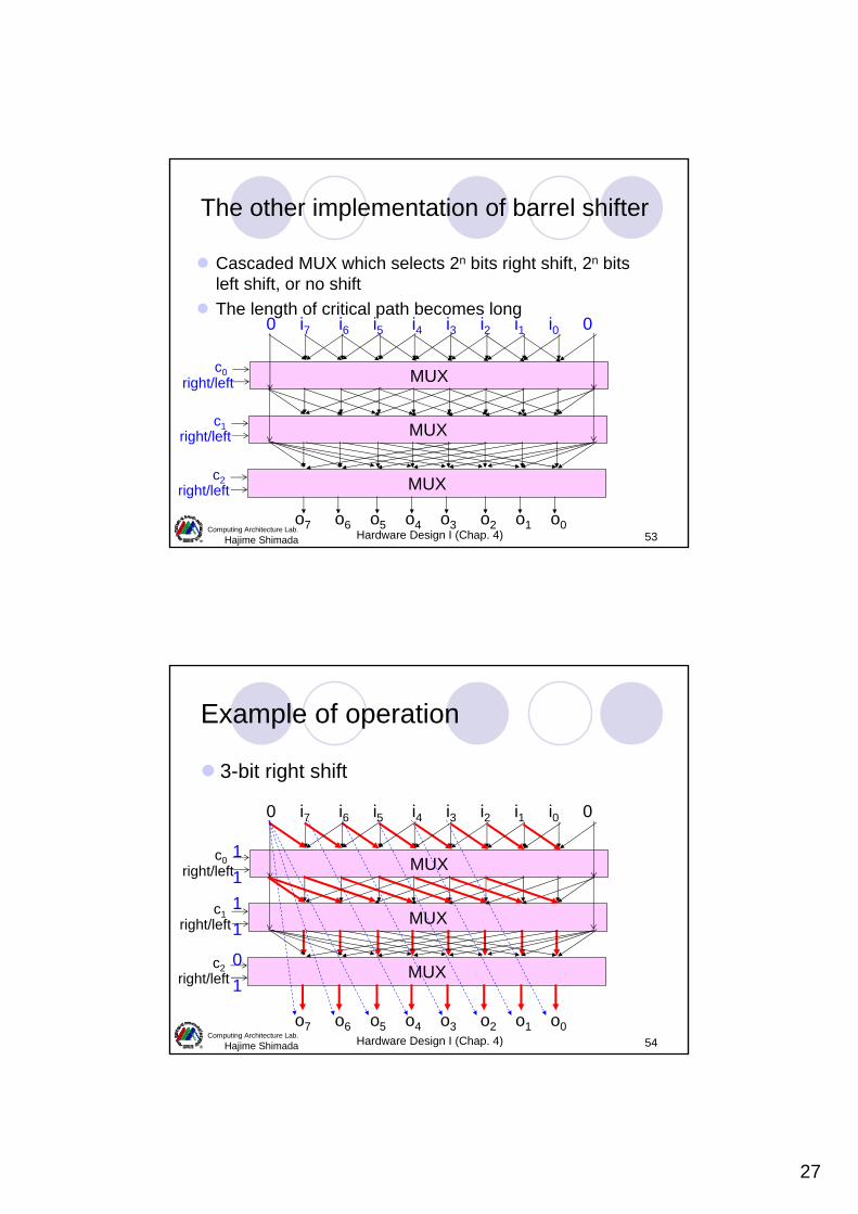
The other implementation of barrel shifter
Cascaded MUX which selects 2n bits right shift, 2n bits left shift, or no shiftThe length of critical path becomes long
MUX
0 i7 i6 i5 i4 i3 i2 i1 i0 0
o7 o6 o5 o4 o3 o2 o1 o0
c0right/left
MUXc1
MUXc2
right/left
right/left
Hardware Design I (Chap. 4) 54Computing Architecture Lab.
Hajime Shimada
Example of operation
3-bit right shift
MUX
0 i7 i6 i5 i4 i3 i2 i1 i0 0
o7 o6 o5 o4 o3 o2 o1 o0
c0right/left
MUXc1
MUXc2
right/left
right/left
1111
01
28
Hardware Design I (Chap. 4) 55Computing Architecture Lab.
Hajime Shimada
...
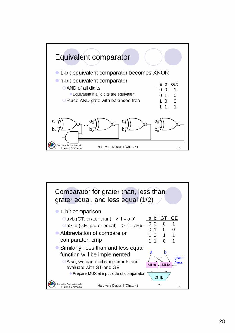
Equivalent comparator
1-bit equivalent comparator becomes XNORn-bit equivalent comparator
AND of all digitsEquivalent if all digits are equivalent
Place AND gate with balanced tree
a b out0 0 10 1 01 0 01 1 1
bn-1
an-1
b2
a2
b1
a1
b0
a0...
Hardware Design I (Chap. 4) 56Computing Architecture Lab.
Hajime Shimada
Comparator for grater than, less than, grater equal, and less equal (1/2)
1-bit comparisona>b (GT: grater than) -> f = a b’a>=b (GE: grater equal) -> f = a+b’
Abbreviation of compare or comparator: cmpSimilarly, less than and less equal function will be implemented
Also, we can exchange inputs and evaluate with GT and GE
Prepare MUX at input side of comparator
a b GT GE0 0 0 10 1 0 01 0 1 11 1 0 1
cmp
MUX MUX
a bgrater/less
29
Hardware Design I (Chap. 4) 57Computing Architecture Lab.
Hajime Shimada
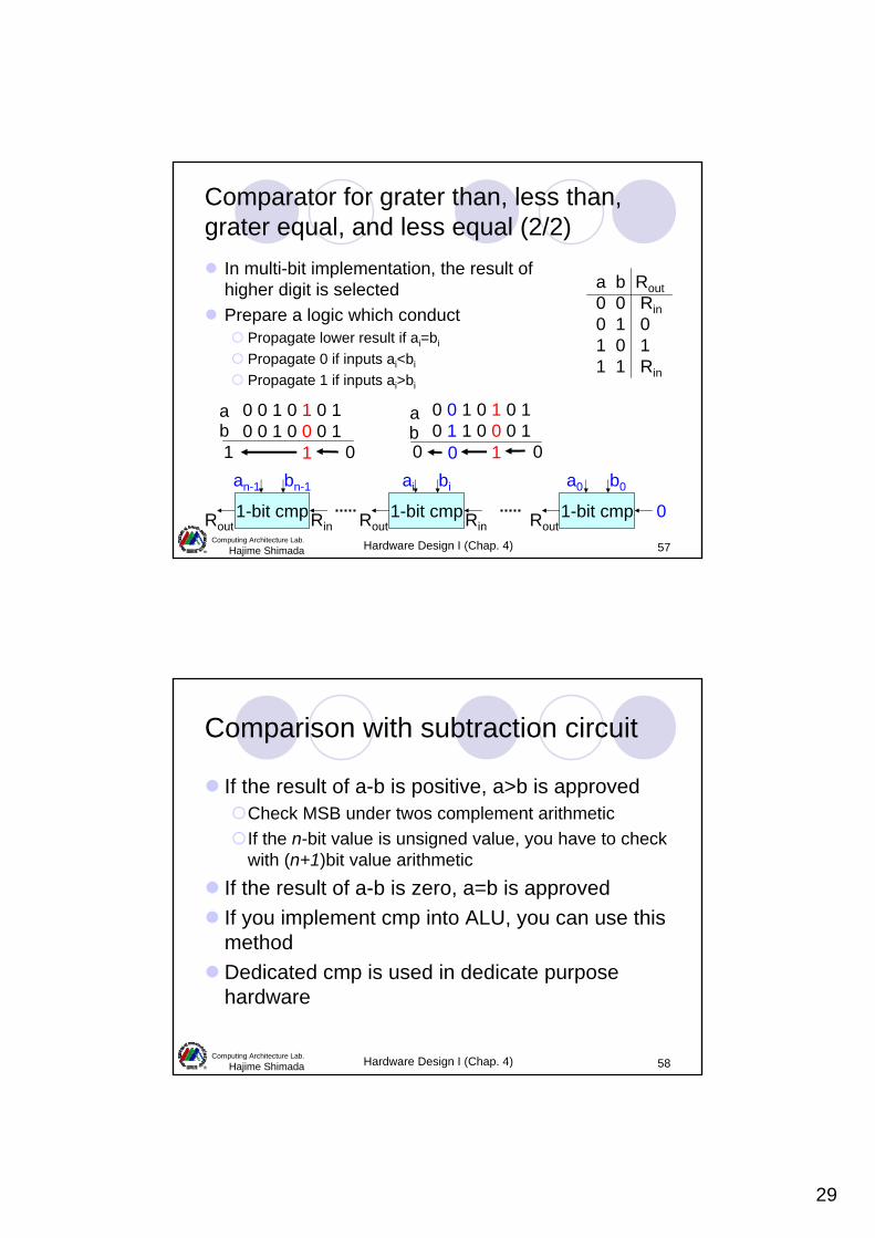
Comparator for grater than, less than, grater equal, and less equal (2/2)
In multi-bit implementation, the result of higher digit is selectedPrepare a logic which conduct
Propagate lower result if ai=bi
Propagate 0 if inputs ai<bi
Propagate 1 if inputs ai>bi
0 0 1 0 1 0 10 0 1 0 0 0 1
1 01
0 0 1 0 1 0 10 1 1 0 0 0 1
1 00 0
0
ab
ab
a b Rout0 0 Rin0 1 01 0 11 1 Rin
RinRout
bn-1an-1
1-bit cmp RinRout
biai
1-bit cmp Rout1-bit cmp
b0a0
Hardware Design I (Chap. 4) 58Computing Architecture Lab.
Hajime Shimada
Comparison with subtraction circuit
If the result of a-b is positive, a>b is approvedCheck MSB under twos complement arithmeticIf the n-bit value is unsigned value, you have to check with (n+1)bit value arithmetic
If the result of a-b is zero, a=b is approvedIf you implement cmp into ALU, you can use this methodDedicated cmp is used in dedicate purpose hardware
30
Hardware Design I (Chap. 4) 59Computing Architecture Lab.
Hajime Shimada
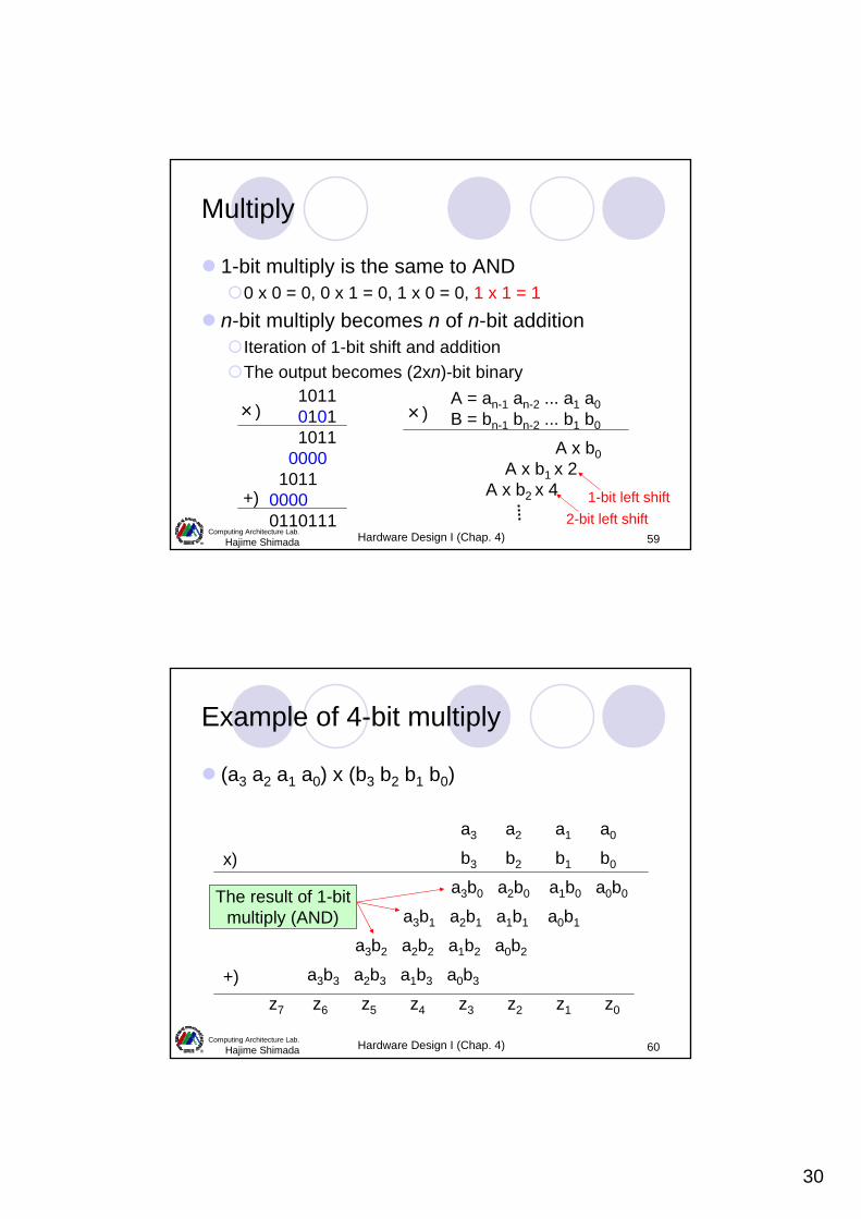
Multiply
1-bit multiply is the same to AND0 x 0 = 0, 0 x 1 = 0, 1 x 0 = 0, 1 x 1 = 1
n-bit multiply becomes n of n-bit additionIteration of 1-bit shift and additionThe output becomes (2xn)-bit binary
101101011011
00001011
00000110111
×)
+)
A = an-1 an-2 ... a1 a0B = bn-1 bn-2 ... b1 b0
×)
A x b0A x b1 x 2
A x b2 x 4 1-bit left shift2-bit left shift
Hardware Design I (Chap. 4) 60Computing Architecture Lab.
Hajime Shimada
Example of 4-bit multiply
(a3 a2 a1 a0) x (b3 b2 b1 b0)
a3 a2 a1 a0
b3 b2 b1 b0
a3b0 a2b0 a1b0 a0b0
a3b1 a2b1 a1b1 a0b1
a3b2 a2b2 a1b2 a0b2
a3b3 a2b3 a1b3 a0b3
z7 z6 z5 z4 z3 z2 z1 z0
x)
+)
The result of 1-bitmultiply (AND)
31
Hardware Design I (Chap. 4) 61Computing Architecture Lab.
Hajime Shimada
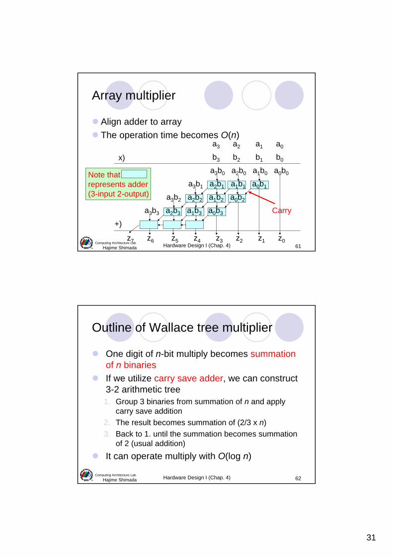
Array multiplier
Align adder to arrayThe operation time becomes O(n)
a3 a2 a1 a0
b3 b2 b1 b0
a3b0 a2b0 a1b0 a0b0
a3b1 a2b1 a1b1 a0b1
a3b2 a2b2 a1b2 a0b2
a3b3 a2b3 a1b3 a0b3
z7 z6 z5 z4 z3 z2 z1 z0
x)
+)
Carry
Note thatrepresents adder(3-input 2-output)
Hardware Design I (Chap. 4) 62Computing Architecture Lab.
Hajime Shimada
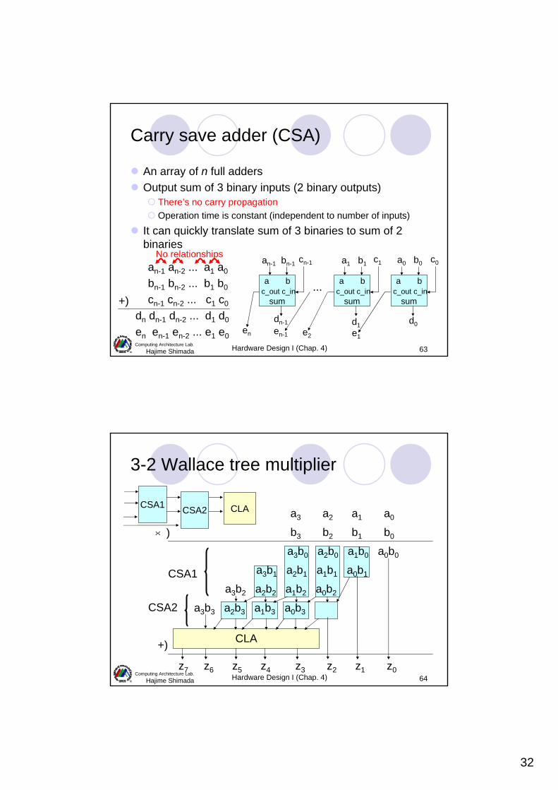
Outline of Wallace tree multiplier
One digit of n-bit multiply becomes summation of n binariesIf we utilize carry save adder, we can construct 3-2 arithmetic tree1. Group 3 binaries from summation of n and apply
carry save addition2. The result becomes summation of (2/3 x n) 3. Back to 1. until the summation becomes summation
of 2 (usual addition)It can operate multiply with O(log n)
32
Hardware Design I (Chap. 4) 63Computing Architecture Lab.
Hajime Shimada
Carry save adder (CSA)
An array of n full addersOutput sum of 3 binary inputs (2 binary outputs)
There’s no carry propagationOperation time is constant (independent to number of inputs)
It can quickly translate sum of 3 binaries to sum of 2 binaries
an-1 an-2 ... a1 a0
bn-1 bn-2 ... b1 b0
cn-1 cn-2 ... c1 c0
dn dn-1 dn-2 ... d1 d0
en en-1 en-2 ... e1 e0
+)
a bc_out c_in
sum
an-1 bn-1
dn-1
...
cn-1
en-1en
a bc_out c_in
sum
a1 b1
d1
c1
e1
a bc_out c_in
sum
a0 b0
d0
c0
e2
No relationships
Hardware Design I (Chap. 4) 64Computing Architecture Lab.
Hajime Shimada
3-2 Wallace tree multiplier
a3 a2 a1 a0
b3 b2 b1 b0
a3b0 a2b0 a1b0 a0b0
a3b1 a2b1 a1b1 a0b1
a3b2 a2b2 a1b2 a0b2
a3b3 a2b3 a1b3 a0b3
z7 z6 z5 z4 z3 z2 z1 z0
×)
+) CLA
CSA1
CSA1 CSA2 CLA
CSA2
33
Hardware Design I (Chap. 4) 65Computing Architecture Lab.
Hajime Shimada
Example of 8-bit multiply
Number of summation becomes 2/3 under one CSAAfter O(log n) of CSAs, it becomes sum of 2 binariesA = a7 a6 ... a1 a0B = b7 b6 ... b1 b0
x )
A x b0A x b1 x 2
A x b2 x 4A x b3 x 8
A x b4 x 16A x b5 x 32
A x b6 x 64A x b7 x 128
CSA
CSA
CSA
CSA CSA CSA
Apply CLA at final
Hardware Design I (Chap. 4) 66Computing Architecture Lab.
Hajime Shimada
Division
Implement computation on paper franklye.g. 107 divided by 3
01101011000000110
0110101100000011
001
000000110000000-)01101011
Cannot subtract 110000000
00000011 x 27
(7-bit left shift)
000000110000000-)01101011
00000011000000-)01101011
0000001100000-)0000000001011
6-bit left shift
5-bit left shift
Can subtract 1100000
Cannot subtract
34
Hardware Design I (Chap. 4) 67Computing Architecture Lab.
Hajime Shimada
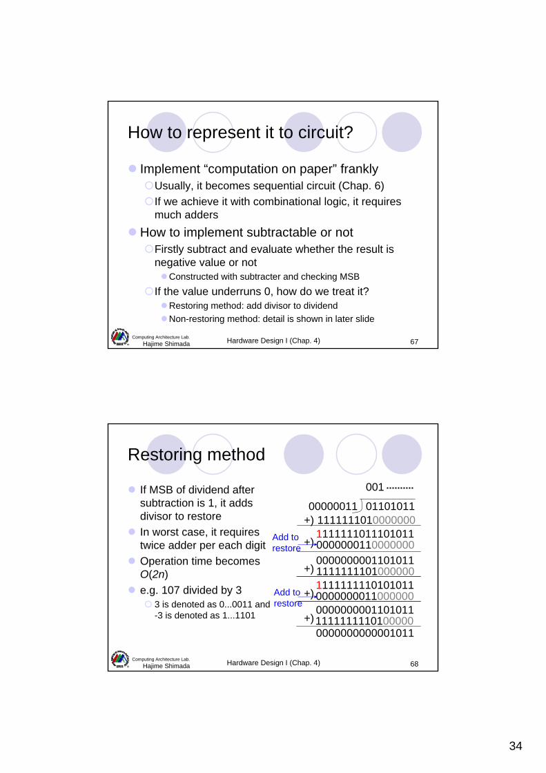
How to represent it to circuit?
Implement “computation on paper” franklyUsually, it becomes sequential circuit (Chap. 6)If we achieve it with combinational logic, it requires much adders
How to implement subtractable or notFirstly subtract and evaluate whether the result is negative value or not
Constructed with subtracter and checking MSB
If the value underruns 0, how do we treat it?Restoring method: add divisor to dividendNon-restoring method: detail is shown in later slide
Hardware Design I (Chap. 4) 68Computing Architecture Lab.
Hajime Shimada
0000000001101011
Restoring method
If MSB of dividend after subtraction is 1, it adds divisor to restoreIn worst case, it requires twice adder per each digitOperation time becomes O(2n)e.g. 107 divided by 3
3 is denoted as 0...0011 and -3 is denoted as 1...1101
0110101100000011
001
1111111010000000+)
00000000011010111111111101000000+)11111111101010110000000011000000+)
Add to restore
Add to restore
1111111011101011+) 0000000110000000
1111111110100000+)0000000000001011

35
Hardware Design I (Chap. 4) 69Computing Architecture Lab.
Hajime Shimada
Non-restoring method
If temporal dividend becomes negative, this method adds following shifted dividendIf temporal dividend is positive
Subtract shifted dividendQuotient becomes 1 if result is positive, otherwise 0
If temporal dividend is negativeAdd shifted dividendQuotient becomes 1 if result is positive, otherwise 0
In some case, we have to compensate reminderOperation time becomes O(n)
Hardware Design I (Chap. 4) 70Computing Architecture Lab.
Hajime Shimada
Example of non-restoring method
Let’s assume 37 divided by 66 is denoted as 0110 and -6 is denoted as 1010
0 0 1 0 0 1 0 1 371 1 0 1 0 0 0 0-6x23
1 1 1 1 0 1 0 1Quotients
00 0 0 1 1 0 0 0+6x22
1 0 0 0 0 1 1 0 111 1 1 1 0 1 0 0-6x21
1 0 0 0 0 0 0 0 111 1 1 1 1 0 1 0-6x20
1 1 1 1 1 0 1 10
1 1 1 1 1 0 1 10 0 0 0 0 1 1 0
If reminder becomes negative, correct remainder by adding +6
1 0 0 0 0 0 0 0 1
Remainder (=1)
-48-11+2413-121
-6
6(0110)
36
Hardware Design I (Chap. 4) 71Computing Architecture Lab.
Hajime Shimada
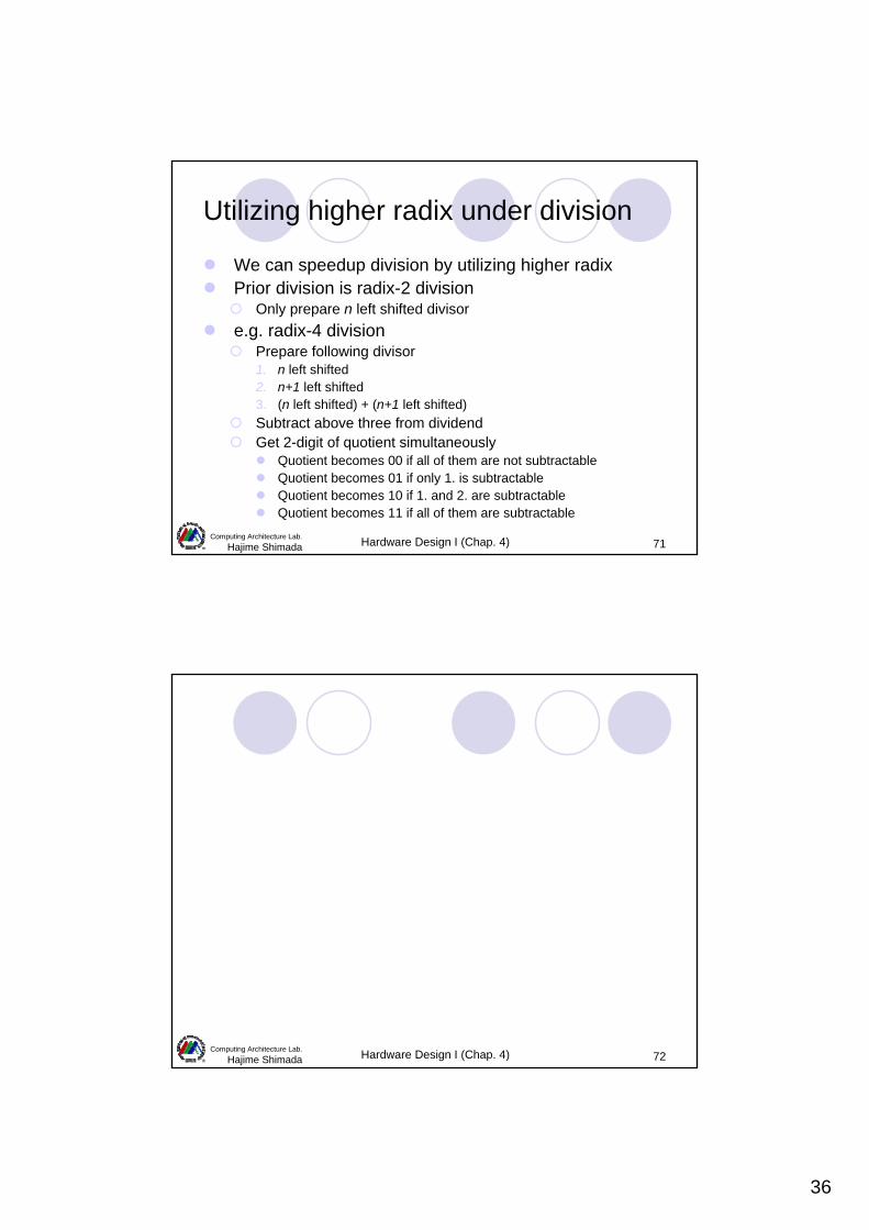
Utilizing higher radix under division
We can speedup division by utilizing higher radixPrior division is radix-2 division
Only prepare n left shifted divisore.g. radix-4 division
Prepare following divisor1. n left shifted2. n+1 left shifted3. (n left shifted) + (n+1 left shifted)Subtract above three from dividendGet 2-digit of quotient simultaneously
Quotient becomes 00 if all of them are not subtractableQuotient becomes 01 if only 1. is subtractableQuotient becomes 10 if 1. and 2. are subtractableQuotient becomes 11 if all of them are subtractable
Hardware Design I (Chap. 4) 72Computing Architecture Lab.
Hajime Shimada
37
Hardware Design I (Chap. 4) 73Computing Architecture Lab.
Hajime Shimada
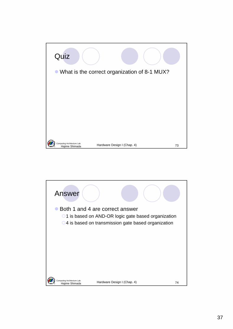
Quiz
What is the correct organization of 8-1 MUX?
Hardware Design I (Chap. 4) 74Computing Architecture Lab.
Hajime Shimada
Answer
Both 1 and 4 are correct answer1 is based on AND-OR logic gate based organization4 is based on transmission gate based organization
38
Hardware Design I (Chap. 4) 75Computing Architecture Lab.
Hajime Shimada
Hardware Design I (Chap. 4) 76Computing Architecture Lab.
Hajime Shimada