Embed Size (px)
Citation preview
3-1.1
PICOBLAZEHardware/Software Interfacing
Slides from Mark Redekopp, EE209 slide set (EE209Spiral3-1.pdf)adopted to suit EE354L
3-1.2
Learning Outcomes• I understand the PicoBlaze bus interface signals: PORT_ID[7:0],
IN_PORT[7:0], OUT_PORT[7:0], READ_STROBE, and WRITE_STROBE• I understand how a memory map provides the agreement between
addresses the software will use and that the hardware must recognize and respond to
• I understand how to build address decoding logic to ensure only the appropriate item/register is selected for a given PORTID
• For output, I can take a memory map and the PORTID and OUT_DATA bits such that the appropriate data is input or saved in a register when an OUTPUT instruction is executed
• For input, I can take a memory map and the appropriate PORTID bits to build logic and muxes such that the appropriate data value is present at IN_DATA when an INPUT instruction is executed
3-1.3
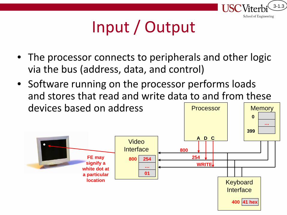
Input / Output
• The processor connects to peripherals and other logic via the bus (address, data, and control)
• Software running on the processor performs loads and stores that read and write data to and from these devices based on address
Video Interface
FE may signify a
white dot at a particular
location
…800
Processor Memory
A D C
800254
WRITE
…0
399
254
01
Keyboard Interface
41 hex400
3-1.4
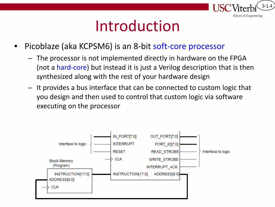
Introduction• Picoblaze (aka KCPSM6) is an 8-bit soft-core processor
– The processor is not implemented directly in hardware on the FPGA (not a hard-core) but instead it is just a Verilog description that is then synthesized along with the rest of your hardware design
– It provides a bus interface that can be connected to custom logic that you design and then used to control that custom logic via software executing on the processor
3-1.5
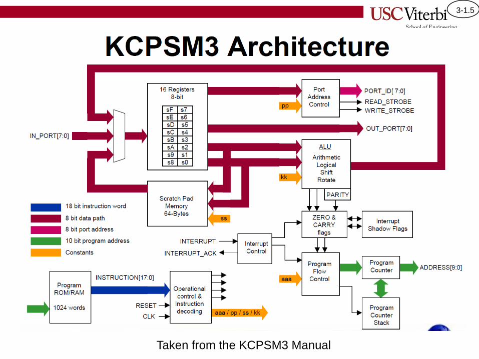
Taken from the KCPSM3 Manual
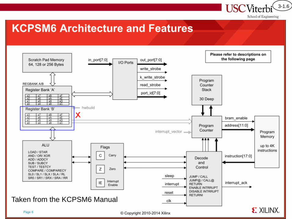
3-1.6
Taken from the KCPSM6 Manual
3-1.7
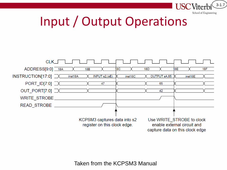
Input / Output Operations
Taken from the KCPSM3 Manual
3-1.8
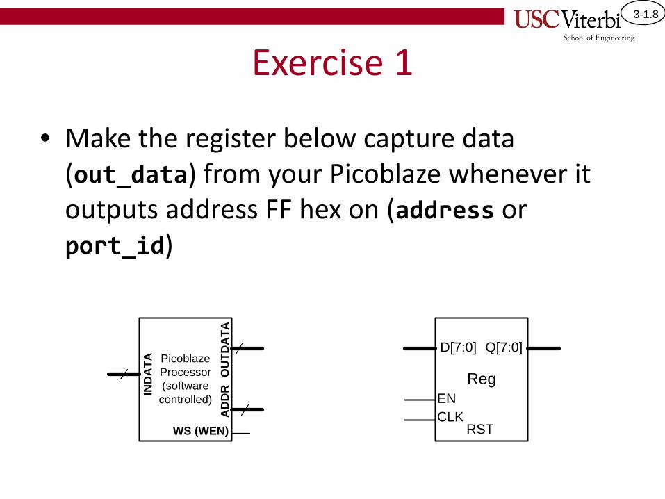
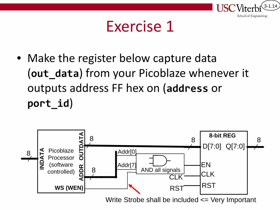
Exercise 1
• Make the register below capture data (out_data) from your Picoblaze whenever it outputs address FF hex on (address or port_id)
PicoblazeProcessor(software
controlled)
OU
TDA
TAA
DD
RIND
ATA
WS (WEN)
RegENCLK
D[7:0] Q[7:0]
RST
3-1.9
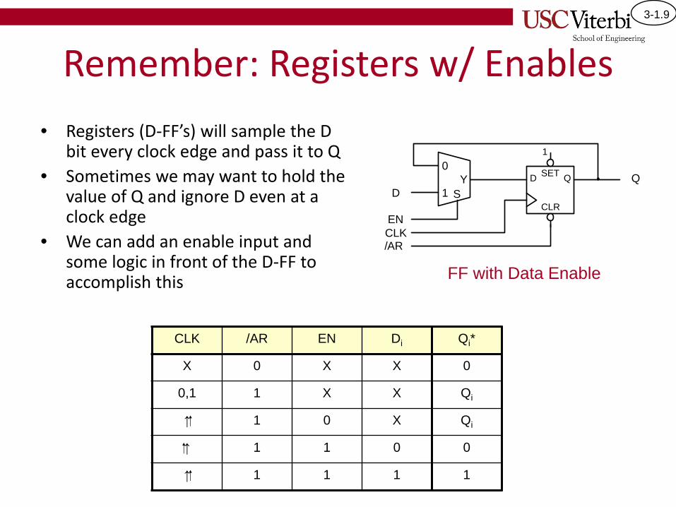
Remember: Registers w/ Enables• Registers (D-FF’s) will sample the D
bit every clock edge and pass it to Q• Sometimes we may want to hold the
value of Q and ignore D even at a clock edge
• We can add an enable input and some logic in front of the D-FF to accomplish this FF with Data Enable
CLK /AR EN Di Qi*
X 0 X X 0
0,1 1 X X Qi
↑ 1 0 X Qi
↑ 1 1 0 0
↑ 1 1 1 1
D Q
CLR
SET
1
DQ
0
1Y
S
ENCLK/AR
3-1.10
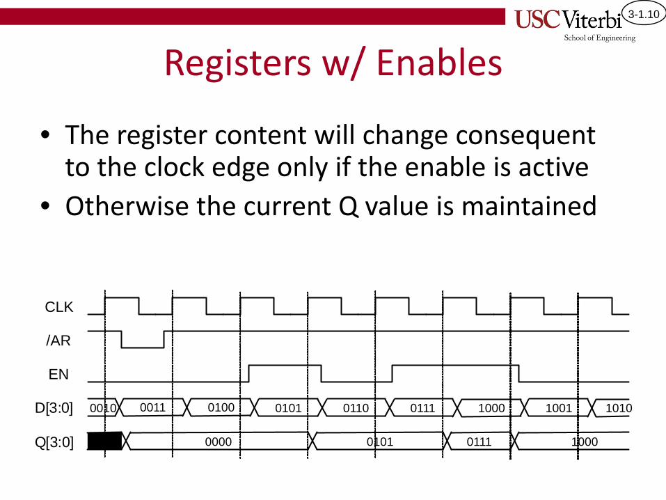
Registers w/ Enables
• The register content will change consequent to the clock edge only if the enable is active
• Otherwise the current Q value is maintained
CLK
/AR
EN
D[3:0]
Q[3:0] 0000 0101 0111 1000
0011 0100 0101 0110 0111 1000 1001 10100010
3-1.11
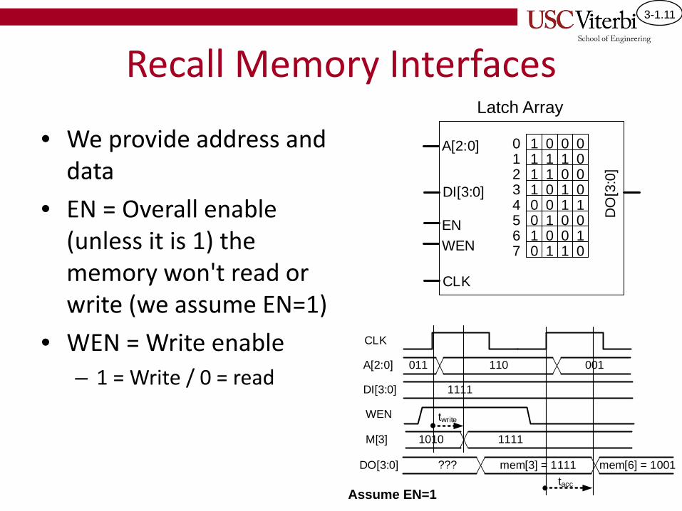
Recall Memory Interfaces
• We provide address and data
• EN = Overall enable (unless it is 1) the memory won't read or write (we assume EN=1)
• WEN = Write enable– 1 = Write / 0 = read
1 0 0 01 1 1 01 1 0 01 0 1 00 0 1 10 1 0 01 0 0 10 1 1 0
01234567
DO
[3:0
]
DI[3:0]
A[2:0]
WEN
CLK
EN
A[2:0]
CLK
110 001
DI[3:0] 1111
WEN
DO[3:0] ??? mem[3] = 1111 mem[6] = 1001
twrite
011
tacc
M[3] 1010 1111
Assume EN=1
Latch Array
3-1.12
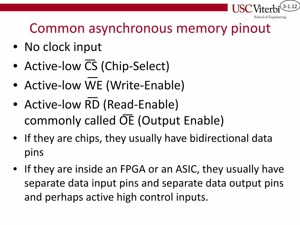
Common asynchronous memory pinout• No clock input• Active-low CS (Chip-Select)• Active-low WE (Write-Enable)• Active-low RD (Read-Enable)
commonly called OE (Output Enable)• If they are chips, they usually have bidirectional data
pins• If they are inside an FPGA or an ASIC, they usually have
separate data input pins and separate data output pins and perhaps active high control inputs.
3-1.13
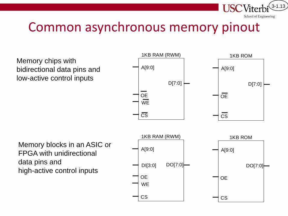
Common asynchronous memory pinout
D[7:0]
A[9:0]
WE
CS
OE
1KB RAM (RWM)
D[7:0]
A[9:0]
CS
OE
1KB ROM
DO[7:0]DI[3:0]
A[9:0]
WE
CS
OE
1KB RAM (RWM)
DO[7:0]
A[9:0]
CS
OE
1KB ROM
Memory chips with bidirectional data pins andlow-active control inputs
Memory blocks in an ASIC or FPGA with unidirectional data pins andhigh-active control inputs
3-1.14
Exercise 1
• Make the register below capture data (out_data) from your Picoblaze whenever it outputs address FF hex on (address or port_id)
PicoblazeProcessor(software
controlled)
OU
TDA
TAA
DD
RIND
ATA
WS (WEN)
ENCLK
D[7:0] Q[7:0]8
8
8
8 88-bit REG
RSTCLKRST
Addr[0]
Addr[7]AND all signals
Write Strobe shall be included <= Very Important
3-1.15
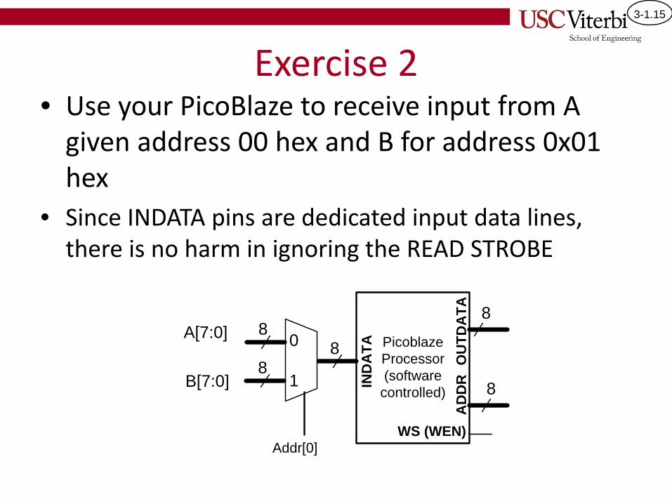
Exercise 2• Use your PicoBlaze to receive input from A
given address 00 hex and B for address 0x01 hex
• Since INDATA pins are dedicated input data lines, there is no harm in ignoring the READ STROBE
PicoblazeProcessor(software controlled)
OU
TDA
TAA
DD
RIND
ATA
WS (WEN)
8
8
80
1
8
8
A[7:0]
B[7:0]
Addr[0]
3-1.16
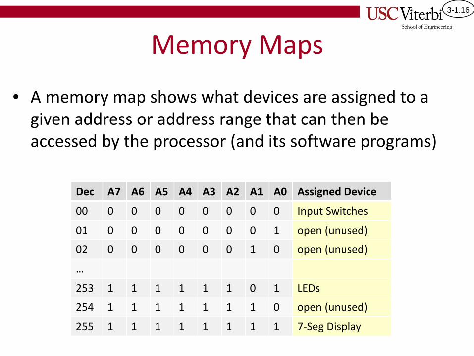
Memory Maps
• A memory map shows what devices are assigned to a given address or address range that can then be accessed by the processor (and its software programs)
Dec A7 A6 A5 A4 A3 A2 A1 A0 Assigned Device
00 0 0 0 0 0 0 0 0 Input Switches
01 0 0 0 0 0 0 0 1 open (unused)
02 0 0 0 0 0 0 1 0 open (unused)
…
253 1 1 1 1 1 1 0 1 LEDs
254 1 1 1 1 1 1 1 0 open (unused)
255 1 1 1 1 1 1 1 1 7-Seg Display
3-1.17
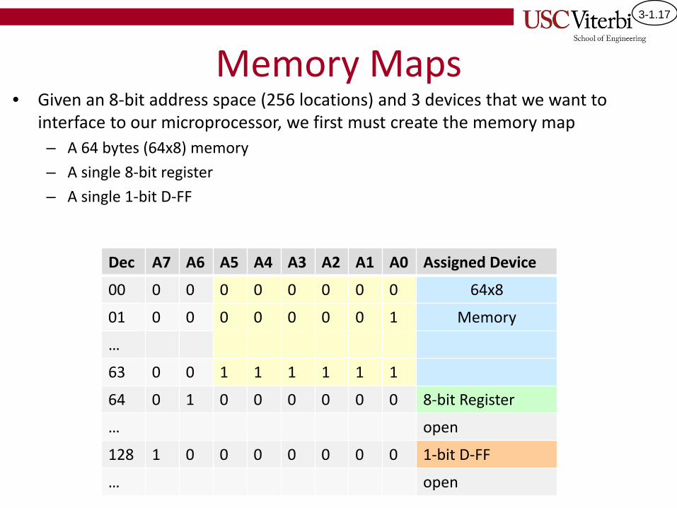
Memory Maps• Given an 8-bit address space (256 locations) and 3 devices that we want to
interface to our microprocessor, we first must create the memory map– A 64 bytes (64x8) memory– A single 8-bit register– A single 1-bit D-FF
Dec A7 A6 A5 A4 A3 A2 A1 A0 Assigned Device
00 0 0 0 0 0 0 0 0 64x8
01 0 0 0 0 0 0 0 1 Memory
…
63 0 0 1 1 1 1 1 1
64 0 1 0 0 0 0 0 0 8-bit Register
… open
128 1 0 0 0 0 0 0 0 1-bit D-FF
… open
3-1.18
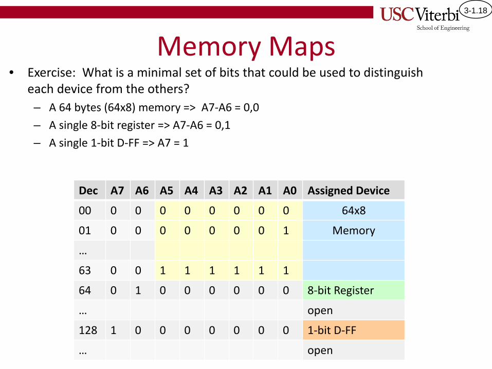
Memory Maps• Exercise: What is a minimal set of bits that could be used to distinguish
each device from the others? – A 64 bytes (64x8) memory => A7-A6 = 0,0– A single 8-bit register => A7-A6 = 0,1– A single 1-bit D-FF => A7 = 1
Dec A7 A6 A5 A4 A3 A2 A1 A0 Assigned Device
00 0 0 0 0 0 0 0 0 64x8
01 0 0 0 0 0 0 0 1 Memory
…
63 0 0 1 1 1 1 1 1
64 0 1 0 0 0 0 0 0 8-bit Register
… open
128 1 0 0 0 0 0 0 0 1-bit D-FF
… open
3-1.19
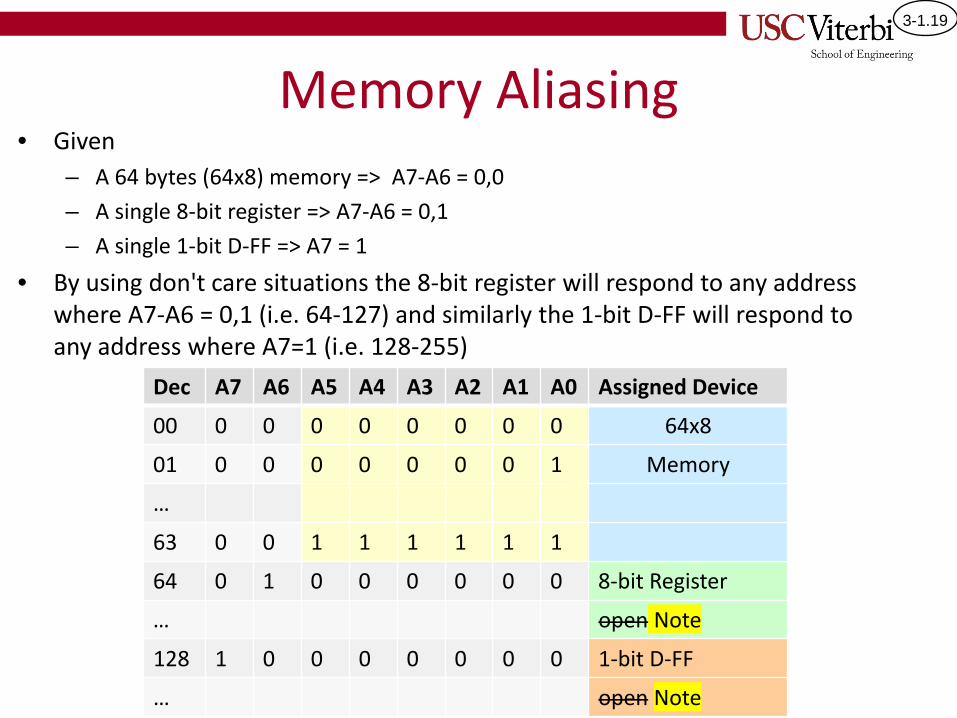
Memory Aliasing• Given
– A 64 bytes (64x8) memory => A7-A6 = 0,0– A single 8-bit register => A7-A6 = 0,1– A single 1-bit D-FF => A7 = 1
• By using don't care situations the 8-bit register will respond to any address where A7-A6 = 0,1 (i.e. 64-127) and similarly the 1-bit D-FF will respond to any address where A7=1 (i.e. 128-255)
Dec A7 A6 A5 A4 A3 A2 A1 A0 Assigned Device
00 0 0 0 0 0 0 0 0 64x8
01 0 0 0 0 0 0 0 1 Memory
…
63 0 0 1 1 1 1 1 1
64 0 1 0 0 0 0 0 0 8-bit Register
… open Note
128 1 0 0 0 0 0 0 0 1-bit D-FF
… open Note
3-1.20
PicoblazeProcessor(software
controlled)O
UTP
OR
TPO
RTI
DINPO
RT
WS (WEN) EN
CLK
D[7:0] Q[7:0]
8
8
88 8
DO[7:0]DI[7:0]
A[5:0]
WEN
CLK
EN
64x8 Memory 88
6
D Q
CLR
SET
0
EN
01
2S1 S0
8-bit REG
1-bit DFF
RST
WS
OUTPORT[7:0]
PortID[7:0]
PortID[6]
WSPortID[7]
PortID[6]
WSPortID[7]
WSPortID[7]
CLK
CLK
OUTPORT[0]
OUTPORT[7:0]
OUTPORT[7:0]
PortID[5:0] MEM[7:0]
REG[7:0]
MEM[7:0]
REG[7:0]
{7'b0000000,FFQ}
RST
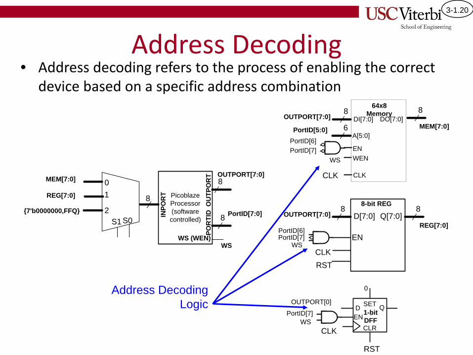
Address Decoding• Address decoding refers to the process of enabling the correct
device based on a specific address combination
Address Decoding Logic
3-1.21
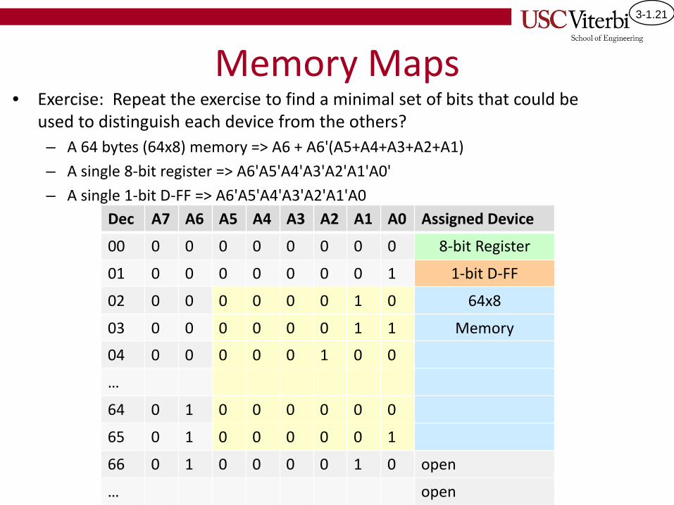
Memory Maps• Exercise: Repeat the exercise to find a minimal set of bits that could be
used to distinguish each device from the others? – A 64 bytes (64x8) memory => A6 + A6'(A5+A4+A3+A2+A1)– A single 8-bit register => A6'A5'A4'A3'A2'A1'A0'– A single 1-bit D-FF => A6'A5'A4'A3'A2'A1'A0
Dec A7 A6 A5 A4 A3 A2 A1 A0 Assigned Device
00 0 0 0 0 0 0 0 0 8-bit Register
01 0 0 0 0 0 0 0 1 1-bit D-FF
02 0 0 0 0 0 0 1 0 64x8
03 0 0 0 0 0 0 1 1 Memory
04 0 0 0 0 0 1 0 0
…
64 0 1 0 0 0 0 0 0
65 0 1 0 0 0 0 0 1
66 0 1 0 0 0 0 1 0 open
… open
3-1.22
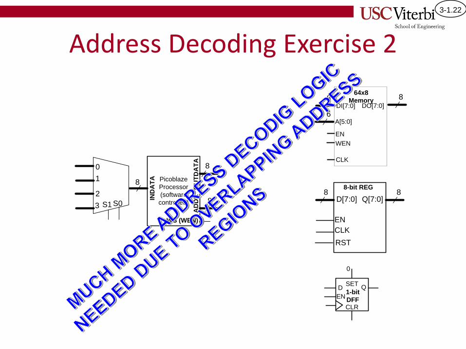
Address Decoding Exercise 2
PicoblazeProcessor(software
controlled)O
UTD
ATA
AD
DRIN
DA
TA
WS (WEN) ENCLK
D[7:0] Q[7:0]
8
8
88 8
DO[7:0]DI[7:0]
A[5:0]
WEN
CLK
EN
64x8 Memory 88
6
D Q
CLR
SET
0
EN
01
23 S1 S0
8-bit REG
1-bit DFF
RST
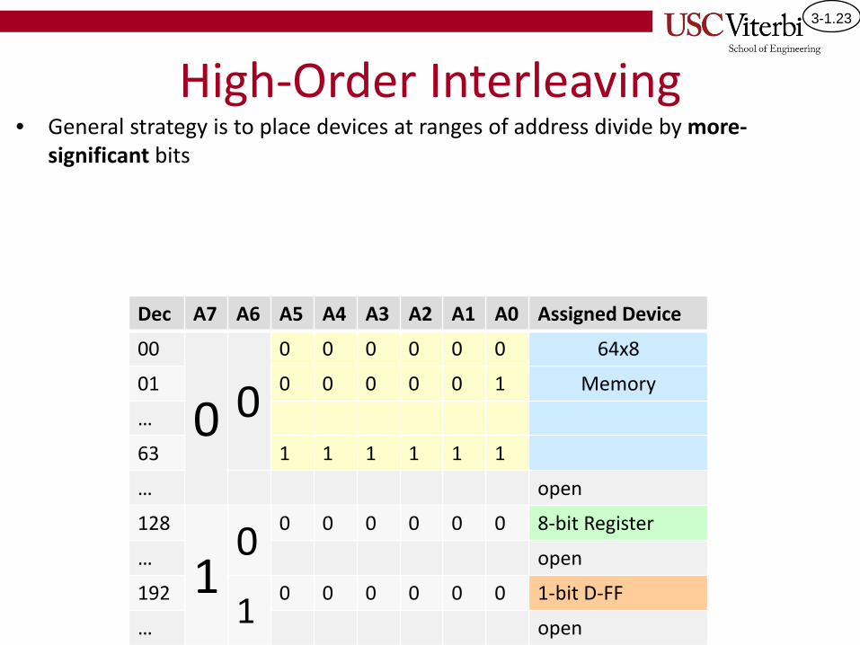
3-1.23
High-Order Interleaving• General strategy is to place devices at ranges of address divide by more-
significant bits
Dec A7 A6 A5 A4 A3 A2 A1 A0 Assigned Device
00
0 00 0 0 0 0 0 64x8
01 0 0 0 0 0 1 Memory
…
63 1 1 1 1 1 1
… open
128
10 0 0 0 0 0 0 8-bit Register
… open
192 1 0 0 0 0 0 0 1-bit D-FF
… open
3-1.24
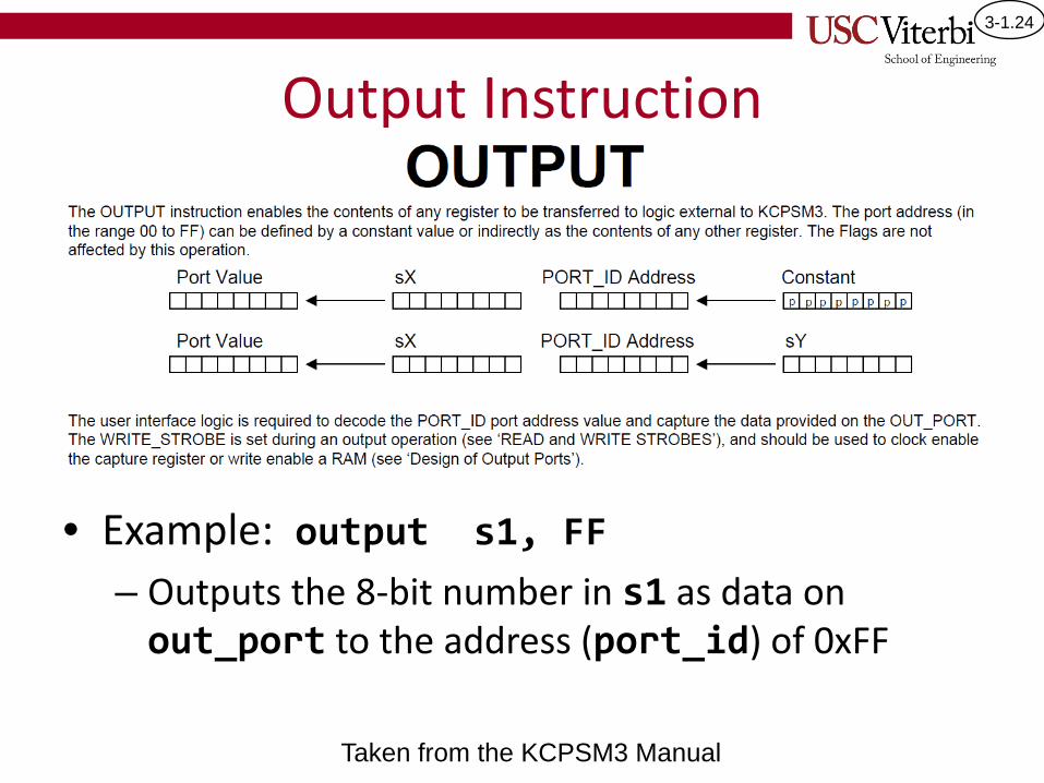
Output Instruction
• Example: output s1, FF– Outputs the 8-bit number in s1 as data on out_port to the address (port_id) of 0xFF
Taken from the KCPSM3 Manual
3-1.25
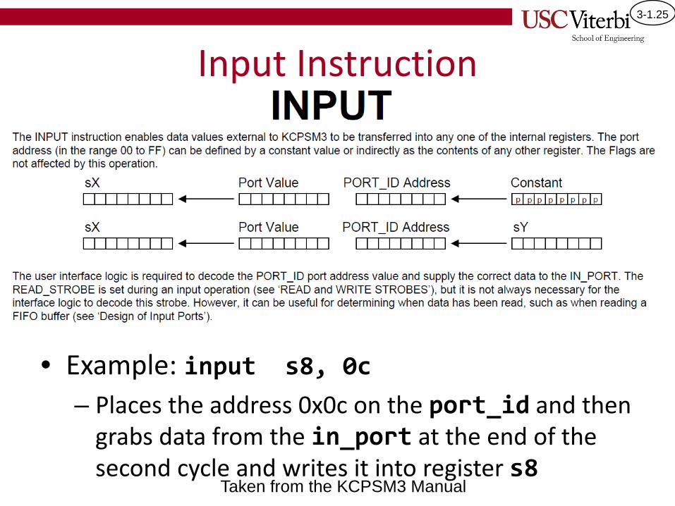
Input Instruction
• Example: input s8, 0c– Places the address 0x0c on the port_id and then
grabs data from the in_port at the end of the second cycle and writes it into register s8
Taken from the KCPSM3 Manual