Embed Size (px)
Citation preview
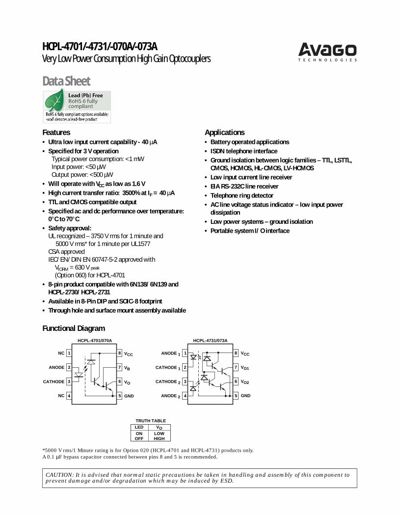
NC
ANODE
CATHODE
NC
VCC
VB
VO
GND
HCPL-4701/070A
VO2
VO1
VCC
GND
ANODE 1
CATHODE 1
CATHODE 2
ANODE 2
7
5
6
8
2
3
4
1
TRUTH TABLELED
ONOFF
VOLOWHIGH
7
5
6
8
2
3
4
1
HCPL-4731/073A
Features• Ultra low input current capability - 40 µA
• Specified for 3 V operationTypical power consumption: <1 mWInput power: <50 µWOutput power: <500 µW
• Will operate with VCC as low as 1.6 V
• High current transfer ratio: 3500% at IF = 40 µA
• TTL and CMOS compatible output
• Specified ac and dc performance over temperature:0°C to 70°C
• Safety approval:UL recognized – 3750 V rms for 1 minute and 5000 V rms* for 1 minute per UL1577CSA approvedIEC/EN/DIN EN 60747-5-2 approved with
VIORM = 630 V peak
(Option 060) for HCPL-4701
• 8-pin product compatible with 6N138/6N139 andHCPL-2730/HCPL-2731
• Available in 8-Pin DIP and SOIC-8 footprint
• Through hole and surface mount assembly available
CAUTION: It is advised that normal static precautions be taken in handling and assembly of this component toprevent damage and/or degradation which may be induced by ESD.
Functional Diagram
*5000 V rms/1 Minute rating is for Option 020 (HCPL-4701 and HCPL-4731) products only.A 0.1 µF bypass capacitor connected between pins 8 and 5 is recommended.
Applications• Battery operated applications
• ISDN telephone interface
• Ground isolation between logic families – TTL, LSTTL,CMOS, HCMOS, HL-CMOS, LV-HCMOS
• Low input current line receiver
• EIA RS-232C line receiver
• Telephone ring detector
• AC line voltage status indicator – low input powerdissipation
• Low power systems – ground isolation
• Portable system I/O interface
HCPL-4701/-4731/-070A/-073AVery Low Power Consumption High Gain Optocouplers
Data Sheet
2
DescriptionThese devices are very low power consumption, highgain single and dual channel optocouplers. TheHCPL-4701 represents the single channel 8-Pin DIPconfiguration and is pin compatible with the industrystandard 6N139. The HCPL-4731 represents the dualchannel 8-Pin DIP configuration and is pincompatible with the popular standard HCPL-2731.The HCPL-070A and HCPL-073A are the equivalentsingle and dual channel products in an SO-8 footprint.Each channel can be driven with an input current aslow as 40 µA and has a typical current transfer ratio of3500%.
These high gain couplers use an AlGaAs LED and anintegrated high gain photodetector to provide anextremely high current transfer ratio between inputand output. Separate pins for the photodiode andoutput stage results in TTL compatible saturationvoltages and high speed operation. Where desired, theVCC and VO terminals may be tied together to achieveconventional Darlington operation (single channelpackage only).
These devices are designed for use in CMOS, LSTTLor other low power applications. They are especiallywell suited for ISDN telephone interface and batteryoperated applications due to the low powerconsumption. A 700% minimum current transfer ratiois guaranteed from 0°C to 70°C operating temperaturerange at 40 µA of LED current and VCC ≥ 3 V.
The SO-8 does not require “through holes” in a PCB.This package occupies approximately one-third thefootprint area of the standard dual-in-line package.The lead profile is designed to be compatible withstandard surface mount processes.
Selection GuideWidebody
8-Pin DIP Package Hermetic(300 Mil) Small Outline SO-8 (400 mil) Single and
Dual Single Dual Minimum Absolute DualSingle Channel Channel Channel Single Input ON Maxi- Channel
Channel Package Package Package Channel Current Minimum mum PackagesPackage HCPL- HCPL- HCPL- Package (IF) CTR VCC HCPL-
6N139[1] 2731[1] 0701[1] 0731[1] HCNW139[1] 0.5 mA 400% 18 V
6N138[1] 2730[1] 0700[1] 0730[1] HCNW138[1] 1.6 mA 300% 7 V
HCPL-4701 4731 070A 0730A 40 µA 800% 18 V
0.5 mA 300% 20 V 5701[1]
5700[1]
5731[1]
5730[1]
Notes:1. Technical data are on separate Avago publication.
3
Ordering InformationHCPL-4701, HCPL-4731, HCPL-070A and HCPL-073A are UL Recognized with 3750 Vrms for 1 minute perUL1577 and are approved under CSA Component Acceptance Notice #5, File CA 88324.
Option
Part RoHS non RoHS Surface Gull Tape UL 5000 Vrms/ IEC/EN/DINNumber Compliant Compliant Package Mount Wing & Reel 1 Minute rating EN 60747-5-2 Quantity
-000E no option 300 mil DIP-8 50 per tube
-300E -300 X X 50 per tube
-500E -500 X X X 1000 per reel
HCPL-4701 -020E -020 X 50 per tube
HCPL-4731 -320E -320 X X X 50 per tube
-520E -520 X X X X 1000 per reel
-060E -060 X 50 per tube
-360E -360 X X X 50 per tube
-560E -560 X X X X 1000 per reel
-000E no option SO-8 100 per tube
HCPL-070A -500E -500 X X X 1500 per reel
HCPL-073A -060E -060 X 100 per tube
-560E -560 X X X X 1500 per reel
To order, choose a part number from the part number column and combine with the desired option fromthe option column to form an order entry.
Example 1:HCPL-4701-560E to order product of 300 mil DIP Gull Wing Surface Mount package in Tape and Reelpackaging with IEC/EN/DIN EN 60747-5-2 Safety Approval and RoHS compliant.
Example 2:HCPL-070A to order product of Surface Mount Small Outline SO-8 package and non RoHS compliant.
Option datasheets are available. Contact your Avago sales representative or authorized distributor forinformation.
Remarks: The notation ‘#XXX’ is used for existing products, while (new) products launched since July15, 2001 and RoHS compliant will use ‘–XXXE.’
4
IF2
6
5GND
3
4
VO2VF2
IO2
+
–
IF1
8
7V
CC1
2
V
O1
ICC
VF1
IO1–
+
SHIELD
USE OF A 0.1 µF BYPASS CAPACITOR CONNECTEDBETWEEN PINS 5 AND 8 IS RECOMMENDED (SEE NOTE 8)
SchematicHCPL-4701 and HCPL-070A HCPL-4731 and HCPL-073A
IF
8VCC
2
3
ICC
VF
ANODE
CATHODE
+
–
VB
IB
6
5GND
VO
IO
7
SHIELD
5
Package Outline Drawings8-Pin DIP Package (HCPL-4701, HCPL-4731)
8-Pin DIP Package with Gull Wing Surface Mount Option 300 (HCPL-4701, HCPL-4731)
9.65 ± 0.25(0.380 ± 0.010)
1.78 (0.070) MAX.1.19 (0.047) MAX.
A XXXXZ
YYWW
DATE CODE
1.080 ± 0.320(0.043 ± 0.013)
2.54 ± 0.25(0.100 ± 0.010)
0.51 (0.020) MIN.
0.65 (0.025) MAX.
4.70 (0.185) MAX.
2.92 (0.115) MIN.
DIMENSIONS IN MILLIMETERS AND (INCHES).
5678
4321
5° TYP.
OPTION CODE*
0.254+ 0.076- 0.051
(0.010+ 0.003)- 0.002)
7.62 ± 0.25(0.300 ± 0.010)
6.35 ± 0.25(0.250 ± 0.010)
TYPE NUMBER
*MARKING CODE LETTER FOR OPTION NUMBERS"L" = OPTION 020"V" = OPTION 060OPTION NUMBERS 300 AND 500 NOT MARKED.
NOTE: FLOATING LEAD PROTRUSION IS 0.25 mm (10 mils) MAX.
3.56 ± 0.13(0.140 ± 0.005)
0.635 ± 0.25(0.025 ± 0.010)
12° NOM.
9.65 ± 0.25(0.380 ± 0.010)
0.635 ± 0.130(0.025 ± 0.005)
7.62 ± 0.25(0.300 ± 0.010)
5678
4321
9.65 ± 0.25(0.380 ± 0.010)
6.350 ± 0.25(0.250 ± 0.010)
1.016 (0.040)
1.27 (0.050)
10.9 (0.430)
2.0 (0.080)
LAND PATTERN RECOMMENDATION
1.080 ± 0.320(0.043 ± 0.013)
3.56 ± 0.13(0.140 ± 0.005)
1.780(0.070)MAX.1.19
(0.047)MAX.
2.54(0.100)BSC
DIMENSIONS IN MILLIMETERS (INCHES).LEAD COPLANARITY = 0.10 mm (0.004 INCHES).
NOTE: FLOATING LEAD PROTRUSION IS 0.25 mm (10 mils) MAX.
0.254+ 0.076- 0.051
(0.010+ 0.003)- 0.002)

6
Small-Outline SO-8 Package (HCPL-070A, HCPL-073A)
XXXYWW
8 7 6 5
4321
5.994 ± 0.203(0.236 ± 0.008)
3.937 ± 0.127(0.155 ± 0.005)
0.406 ± 0.076(0.016 ± 0.003) 1.270
(0.050)BSC
* 5.080 ± 0.127(0.200 ± 0.005)
3.175 ± 0.127(0.125 ± 0.005) 1.524
(0.060)
45° X0.432
(0.017)
0.228 ± 0.025(0.009 ± 0.001)
TYPE NUMBER(LAST 3 DIGITS)
DATE CODE
0.305(0.012)
MIN.* TOTAL PACKAGE LENGTH (INCLUSIVE OF MOLD FLASH) 5.207 ± 0.254 (0.205 ± 0.010)
DIMENSIONS IN MILLIMETERS (INCHES).LEAD COPLANARITY = 0.10 mm (0.004 INCHES) MAX.
0.203 ± 0.102(0.008 ± 0.004)
7°
NOTE: FLOATING LEAD PROTRUSION IS 0.15 mm (6 mils) MAX.
7.49 (0.295)
1.9 (0.075)
0.64 (0.025)
LAND PATTERN RECOMMENDATION
PIN ONE
Solder Reflow Thermal Profile
0
TIME (SECONDS)
TE
MP
ER
AT
UR
E (
°C)
200
100
50 150100 200 250
300
0
30SEC.
50 SEC.
30SEC.
160°C
140°C150°C
PEAKTEMP.245°C
PEAKTEMP.240°C
PEAKTEMP.230°C
SOLDERINGTIME200°C
PREHEATING TIME150°C, 90 + 30 SEC.
2.5°C ± 0.5°C/SEC.
3°C + 1°C/–0.5°C
TIGHTTYPICALLOOSE
ROOMTEMPERATURE
PREHEATING RATE 3°C + 1°C/–0.5°C/SEC.REFLOW HEATING RATE 2.5°C ± 0.5°C/SEC.
Figure 1a. Solder Reflow Thermal Profile.
Note: Non-halide flux should be used.
7
Regulatory InformationThe HCPL-4701/4731 and HCPL-070A/073A have been approvedby the following organizations:
ULRecognized under UL 1577,Component RecognitionProgram, File E55361.
CSAApproved under CSA ComponentAcceptance Notice #5, File CA88324.
IEC/EN/DIN EN 60747-5-2Approved under:IEC 60747-5-2:1997 + A1:2002EN 60747-5-2:2001 + A1:2002DIN EN 60747-5-2 (VDE 0884 Teil 2):2003-01.(Option 060 only)
Insulation Related Specifications8-Pin DIP(300 Mil) SO-8
Parameter Symbol Value Value Units ConditionsMinimum External Air L(101) 7.1 4.9 mm Measured from input terminals toGap (External output terminals, shortest distanceClearance) through air.Minimum External L(102) 7.4 4.8 mm Measured from input terminals toTracking (External output terminals, shortest distanceCreepage) path along body.Minimum Internal Plastic 0.08 0.08 mm Through insulation distance, conductorGap (Internal Clearance) to conductor, usually the direct
distance between the photoemitter andphotodetector inside the optocouplercavity.
Tracking Resistance CTI 200 200 Volts DIN IEC 112/ VDE 0303 Part 1(Comparative TrackingIndex)Isolation Group IIIa IIIa Material Group DIN VDE 0110,
1/89, Table 1)
Option 300 – surface mount classification is Class A in accordance with CECC 00802.
Figure 1b. Pb-Free IR Profile.
Recommended Pb-Free IR Profile
217 °C
RAMP-DOWN6 °C/SEC. MAX.
RAMP-UP3 °C/SEC. MAX.
150 - 200 °C
260 +0/-5 °C
t 25 °C to PEAK
60 to 150 SEC.
20-40 SEC.
TIME WITHIN 5 °C of ACTUALPEAK TEMPERATURE
tp
tsPREHEAT
60 to 180 SEC.
tL
TL
TsmaxTsmin
25
Tp
TIME
TE
MP
ER
AT
UR
E
NOTES:THE TIME FROM 25 °C to PEAK TEMPERATURE = 8 MINUTES MAX.Tsmax = 200 °C, Tsmin = 150 °C
Note: Non-halide flux should be used.
8
IEC/EN/DIN EN 60747-5-2 Insulation Related Characteristics (HCPL-4701 OPTION 060 ONLY)
Description Symbol Characteristic Units
Installation classification per DIN VDE 0110/1.89, Table 1for rated mains voltage ≤ 300 V rms I-IV
for rated mains voltage ≤ 450 V rms I-III
Climatic Classification 55/85/21
Pollution Degree (DIN VDE 0110/1.89) 2
Maximum Working Insulation Voltage VIORM 630 V peak
Input to Output Test Voltage, Method b*VIORM x 1.87 = VPR, 100% Production Test with tm = 1 sec, VPR 1181 V peak
Partial Discharge < 5 pC
Input to Output Test Voltage, Method a*VIORM x 1.5 = VPR, Type and sample test, VPR 945 V peak
tm = 60 sec, Partial Discharge < 5 pC
Highest Allowable Overvoltage*(Transient Overvoltage, tini = 10 sec) VIOTM 6000 V peak
Safety Limiting Values(Maximum values allowed in the event of a failure,also see Figure 16, Thermal Derating curve.)
Case Temperature TS 175 °CInput Current IS,INPUT 230 mAOutput Power PS,OUTPUT 600 mW
Insulation Resistance at TS, VIO = 500 V RS >109 Ω
*Refer to the front of the optocoupler section of the current catalog, under Product Safety Regulations section, IEC/EN/DIN EN60747-5-2, for a detailed description.Note: Isolation characteristics are guaranteed only within the safety maximum ratings which must be ensured by protective circuits inapplication.
9
Absolute Maximum Ratings(No Derating Required up to 70°C)
Parameter Symbol Minimum Maximum Units
Storage Temperature TS -55 125 °C
Operating Temperature TA -40 85 °C
Average Forward Input Current (HCPL-4701/4731) IF(AVG) 10 mA
Average Forward Input Current (HCPL-070A/073A) IF(AVG) 5 mA
Peak Transient Input Current (HCPL-4701/4731) IFPK 20 mA(50% Duty Cycle, 1 ms Pulse Width)
Peak Transient Input Current (HCPL-070A/073A) IFPK 10 mA(50% Duty Cycle, 1 ms Pulse Width)
Reverse Input Voltage VR 2.5 V
Input Power Dissipation (Each Channel) PI 15 mW
Output Current (Each Channel) IO 60 mA
Emitter Base Reverse Voltage (HCPL-4701/070A) VEB 0.5 V
Output Transistor Base Current (HCPL-4701/070A) IB 5 mA
Supply Voltage VCC -0.5 18 V
Output Voltage VO -0.5 18 V
Output Power Dissipation (Each Channel) PO 100 mW
Total Power Dissipation (Each Channel) PT 115 mW
Lead Solder Temperature (for Through Hole Devices) 260°C for 10 sec., 1.6 mm below seating plane
Reflow Temperature Profile See Package Outline Drawings section(for SOIC-8 and Option #300)
Recommended Operating Conditions
Parameter Symbol Min. Max. Units
Power Supply Voltage VCC* 1.6 18 V
Forward Input Current (ON) IF(ON) 40 5000 µA
Forward Input Voltage (OFF) VF(OFF) 0 0.8 V
Operating Temperature TA 0 70 °C
*See Note 1.

10
Electrical Specifications0°C ≤ TA ≤ 70°C, 4.5 V ≤ VCC ≤ 20 V, 1.6 mA ≤ IF(ON) ≤ 5 mA, 0 V ≤ VF(OFF) ≤ 0.8 V, unless otherwisespecified. All Typicals at TA = 25°C. See note 8.
Device Parameter Symbol HCPL- Min. Typ.* Max. Units Test Conditions Fig. Note
Current CTR 800 3500 25k % IF = 40 µA, VO = 0.4 V 4, 5 2Transfer VCC = 4.5 V
600 3000 8k IF = 0.5 mA,VCC = 4.5 V
700 3200 25k IF = 40 µA500 2700 8k IF = 0.5 mA
Logic Low VOL 0.06 0.4 V IF = 40 µA, IO = 280 µA 2, 30.04 0.4 IF = 0.5 mA, IO = 2.5 mA
Logic High IOH 0.01 5 µA VO = VCC = 3 to 7 V,Output Current IF = 0 mA
0.02 80 VO = VCC = 18 V,IF = 0 mA
Logic Low ICCL 4701/070A 0.02 0.2 mA IF = 40 µA VO = Open0.1 1 IF = 0.5 mA
4731/073A 0.04 0.4 IF = 40 µA0.2 2.0 IF = 0.5 mA
Logic High ICCH 4701/070A <0.01 10 µA IF = 0 mA VO = Open4731/073A <0.01 20
Input Forward VF 1.1 1.25 1.4 V IF = 40 to 500 µA, 6Voltage TA = 25°C
0.95 1.5 IF = 40 to 500 µA
Input Reverse BVR 3.0 5.0 V IR = 100 µA, TA = 25°C
2.5 IR = 100 µA
Temperature ∆VF/∆TA -2.0 mV/°C IF = 40 µA
-1.6 IF = 0.5 mA
Input Capacitance CIN 18 pF f = 1 MHz, VF = 0 V
*All typical values at TA = 25°C and VCC = 5 V, unless otherwise noted.
Ratio
Supply Current
Supply Current
Output Voltage
Coefficient ofForward Voltage
BreakdownVoltage
11
Package Characteristics
DeviceParameter Symbol HCPL- Min. Typ.* Max. Units Test Conditions Fig. Note
Input-Output Momentary VISO 3750 V rms RH ≤ 50%, 3, 4Withstand Voltage** t = 1 min.,
Option 020 4701 5000 3, 4a4731
Resistance RI-O 1012 Ω VI-O = 500 VDC 3(Input-Output) RH ≤ 45%
Capacitance CI-O 0.6 pF f = 1 MHz 3(Input-Output)
Insulation Leakage II-I 4731 0.005 µA RH ≤ 45%, t = 5 s, 5Current (Input-Input) 073A VI-I = 500 VDC
Resistance (Input-Input) RI-I 1011 Ω
Capacitance CI-I 4731 0.03 pF f = 1 MHz 5(Input-Input) 073A 0.25
*All typical values at TA = 25°C and VCC = 5 V.**The Input-Output Momentary Withstand Voltage is a dielectric voltage rating that should not be interpreted as an input-outputcontinuous voltage rating. For the continuous voltage rating refer to the IEC/EN/DIN EN 60747-5-2 Insulation CharacteristicsTable (if applicable), your equipment level safety specification or Avago Application Note 1074 entitled “Optocoupler Input-OutputEndurance Voltage.”
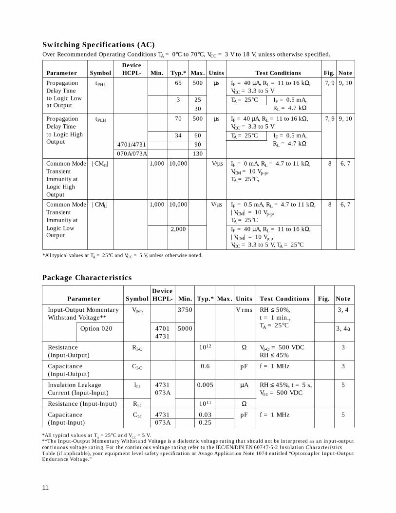
Switching Specifications (AC)Over Recommended Operating Conditions TA = 0°C to 70°C, VCC = 3 V to 18 V, unless otherwise specified.
DeviceParameter Symbol HCPL- Min. Typ.* Max. Units Test Conditions Fig. Note
Propagation tPHL 65 500 µs IF = 40 µA, RL = 11 to 16 kΩ, 7, 9 9, 10Delay Time VCC = 3.3 to 5 V
3 25 TA = 25°C IF = 0.5 mA,30
Propagation tPLH 70 500 µs IF = 40 µA, RL = 11 to 16 kΩ, 7, 9 9, 10Delay Time VCC = 3.3 to 5 V
34 60 TA = 25°C IF = 0.5 mA,4701/4731 90070A/073A 130
Common Mode |CMH| 1,000 10,000 V/µs IF = 0 mA, RL = 4.7 to 11 kΩ, 8 6, 7Transient VCM = 10 Vp-p,Immunity at TA = 25°C,Logic HighOutput
Common Mode |CML| 1,000 10,000 V/µs IF = 0.5 mA, RL = 4.7 to 11 kΩ, 8 6, 7Transient |VCM| = 10 Vp-p,Immunity at TA = 25°C
2,000 IF = 40 µA, RL = 11 to 16 kΩ,|VCM| = 10 Vp-pVCC = 3.3 to 5 V, TA = 25°C
*All typical values at TA = 25°C and VCC = 5 V, unless otherwise noted.
to Logic Lowat Output RL = 4.7 kΩ
to Logic HighOutput RL = 4.7 kΩ
Logic LowOutput
TA = 25°C
12
Notes:1. Specification information is available
form the factory for 1.6 V operation.Call your local field sales office forfurther information.
2. DC CURRENT TRANSFER RATIO isdefined as the ratio of outputcollector current, IO, to the forwardLED input current, IF, times 100%.
3. Device considered a two terminaldevice: pins 1, 2, 3, and 4 shortedtogether, and pins 5, 6, 7, and 8shorted together.
4. In accordance with UL 1577, eachoptocoupler is proof tested byapplying an insulation test voltage≥ 4500 VRMS for 1 second (leakagedetection current limit, II-O ≤ 5 µA.
4a. In accordance with UL 1577, eachoptocoupler is proof tested byapplying an insulation test voltage≥ 6000 VRMS for 1 second (leakage
detection current limit, II-O ≤ 5 µA.This test is performed before the100% production test for partialdischarge (Method b) shown in theIEC/EN/DIN EN 60747-5-2 InsulationCharacteristics Table.
5. Measured between pins 1 and 2shorted together, and pins 3 and 4shorted together.
6. Common transient immunity in aLogic High level is the maximumtolerable (positive) dVCM/dt on theleading edge of the common modepulse, VCM, to assure that the outputwill remain in a Logic High state (i.e.,VO > 2.0 V). Common transientimmunity in a Logic Low level is hemaximum tolerable (negative)dVCM/dt on the trailing edge of thecommon mode pulse, VCM, to assurethat the output will remain in a LogicLow state (i.e., VO < 0.8 V).
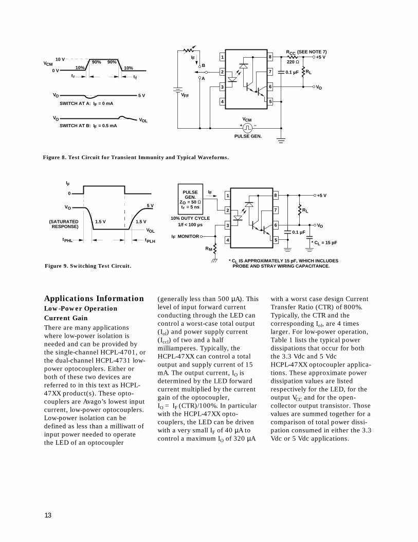
7. In applications where dV/dt mayexceed 50,000 V/µs (such as staticdischarge) a series resistor, RCC,should be included to protect thedetector IC form destructively highsurge currents. The recommendedvalue is RCC = 220 Ω.
8. Use of a 0.1 µF bypass capacitor con-nected between pins 8 and 5 adjacentto the device is recommended.
9. Pin 7 open for single channel product.10. Use of resistor between pins 5 and 7
will decrease gain and delay time.Significant reduction in overall gaincan occur when using resistor valuesbelow 47 kΩ for single channelproduct.
11. The Applications Information sectionof this data sheet references theHCPL-47XX part family, but appliesequally to the HCPL-070A and HCPL-073A parts.
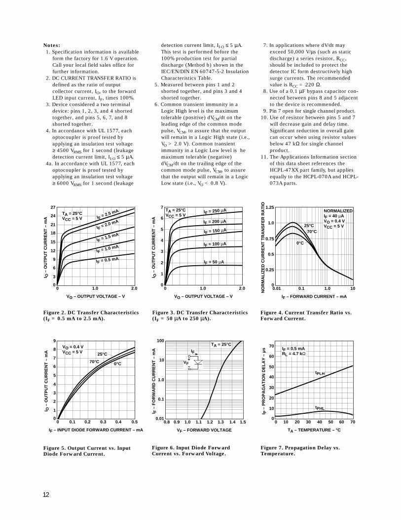
Figure 2. DC Transfer Characteristics(IF = 0.5 mA to 2.5 mA).
Figure 3. DC Transfer Characteristics(IF = 50 µA to 250 µA).
Figure 4. Current Transfer Ratio vs.Forward Current.
Figure 5. Output Current vs. InputDiode Forward Current.
Figure 6. Input Diode ForwardCurrent vs. Forward Voltage.
Figure 7. Propagation Delay vs.Temperature.
I O –
OU
TP
UT
CU
RR
EN
T –
mA
0
7
0
VO – OUTPUT VOLTAGE – V
2.0
6
5
4
3
2
1
1.0
TA = 25°CVCC = 5 V
IF = 250 µA
IF = 200 µA
IF = 150 µA
IF = 100 µA
IF = 50 µA
I F –
FO
RW
AR
D C
UR
RE
NT
– m
A
0.80.01
VF – FORWARD VOLTAGE
1.5
10
1.0
0.1
0.9 1.3
100
1.0 1.1 1.2 1.4
TA = 25°C
IF
VF+
–
I O –
OU
TP
UT
CU
RR
EN
T –
mA
0
27
0
VO – OUTPUT VOLTAGE – V
2.0
24
21
18
15
12
9
6
3
1.0
TA = 25°CVCC = 5 V IF = 2.5 mA
IF = 2.0 mA
IF = 1.5 mA
IF = 1.0 mA
IF = 0.5 mAN
OR
MA
LIZ
ED
CU
RR
EN
T T
RA
NS
FE
R R
AT
IO
0.01
1.25
0
IF – FORWARD CURRENT – mA
10
0.75
0.5
0.25
0.1 1.0
1.025°C
70°C
0°C
NORMALIZEDIF = 40 µAVO = 0.4 VVCC = 5 V
I O –
OU
TP
UT
CU
RR
EN
T –
mA
0
9
0
IF – INPUT DIODE FORWARD CURRENT – mA
0.5
8
7
6
5
4
3
2
1
0.1
VO = 0.4 VVCC = 5 V
0.2 0.3 0.4
25°C
0°C70°C
I P –
PR
OP
AG
AT
ION
DE
LA
Y –
µs
00
TA – TEMPERATURE – °C
70
70
60
50
40
30
20
10
50
IF = 0.5 mARL = 4.7 kΩ
10 20 30 40 60
tPLH
tPHL
13
Figure 9. Switching Test Circuit.
Applications InformationLow-Power OperationCurrent GainThere are many applicationswhere low-power isolation isneeded and can be provided bythe single-channel HCPL-4701, orthe dual-channel HCPL-4731 low-power optocouplers. Either orboth of these two devices arereferred to in this text as HCPL-47XX product(s). These opto-couplers are Avago’s lowest inputcurrent, low-power optocouplers.Low-power isolation can bedefined as less than a milliwatt ofinput power needed to operatethe LED of an optocoupler
(generally less than 500 µA). Thislevel of input forward currentconducting through the LED cancontrol a worst-case total output(Iol) and power supply current(Iccl) of two and a halfmilliamperes. Typically, theHCPL-47XX can control a totaloutput and supply current of 15mA. The output current, IO isdetermined by the LED forwardcurrent multiplied by the currentgain of the optocoupler,IO = IF (CTR)/100%. In particularwith the HCPL-47XX opto-couplers, the LED can be drivenwith a very small IF of 40 µA tocontrol a maximum IO of 320 µA
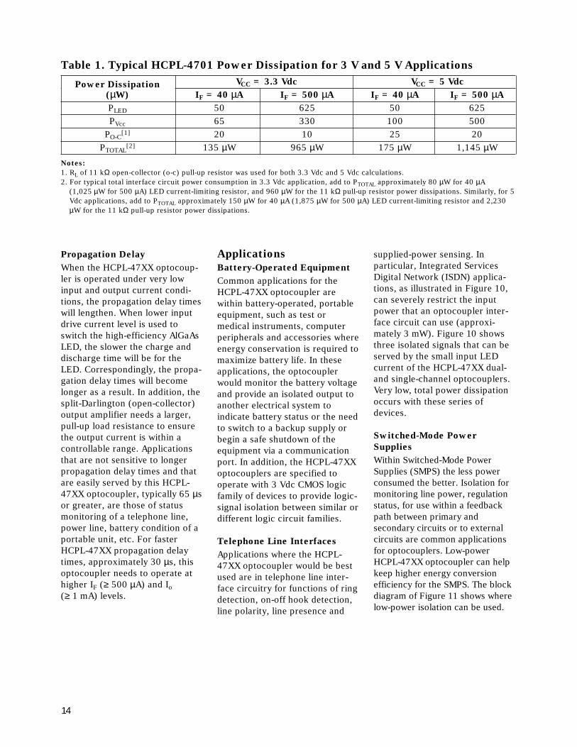
with a worst case design CurrentTransfer Ratio (CTR) of 800%.Typically, the CTR and thecorresponding Iol, are 4 timeslarger. For low-power operation,Table 1 lists the typical powerdissipations that occur for boththe 3.3 Vdc and 5 VdcHCPL-47XX optocoupler applica-tions. These approximate powerdissipation values are listedrespectively for the LED, for theoutput VCC and for the open-collector output transistor. Thosevalues are summed together for acomparison of total power dissi-pation consumed in either the 3.3Vdc or 5 Vdc applications.
VO
PULSEGEN.
Z = 50 Ωt = 5 nsOr
I MONITORF
IF
0.1 µF
LR
* CL = 15 pF RM
0
tPHL tPLH
OV
IF
OLV
1.5 V 1.5 V
5 V7
1
2
3
4 5
6
8
10% DUTY CYCLE1/f < 100 µs
(SATURATEDRESPONSE)
* CL IS APPROXIMATELY 15 pF, WHICH INCLUDES PROBE AND STRAY WIRING CAPACITANCE.
+5 V
Figure 8. Test Circuit for Transient Immunity and Typical Waveforms.
VO
IF
LR
A
B
PULSE GEN.
VCM+
VFFOV
OLVOV
0 V10%
90% 90%10%
SWITCH AT A: I = 0 mAF
SWITCH AT B: I = 0.5 mAF
CMV
tr tf
5 V
+5 V
–
7
1
2
3
4 5
6
8RCC (SEE NOTE 7)
10 V
0.1 µF
220 Ω
14
Propagation DelayWhen the HCPL-47XX optocoup-ler is operated under very lowinput and output current condi-tions, the propagation delay timeswill lengthen. When lower inputdrive current level is used toswitch the high-efficiency AlGaAsLED, the slower the charge anddischarge time will be for theLED. Correspondingly, the propa-gation delay times will becomelonger as a result. In addition, thesplit-Darlington (open-collector)output amplifier needs a larger,pull-up load resistance to ensurethe output current is within acontrollable range. Applicationsthat are not sensitive to longerpropagation delay times and thatare easily served by this HCPL-47XX optocoupler, typically 65 µsor greater, are those of statusmonitoring of a telephone line,power line, battery condition of aportable unit, etc. For fasterHCPL-47XX propagation delaytimes, approximately 30 µs, thisoptocoupler needs to operate athigher IF (≥ 500 µA) and Io(≥ 1 mA) levels.
ApplicationsBattery-Operated EquipmentCommon applications for theHCPL-47XX optocoupler arewithin battery-operated, portableequipment, such as test ormedical instruments, computerperipherals and accessories whereenergy conservation is required tomaximize battery life. In theseapplications, the optocouplerwould monitor the battery voltageand provide an isolated output toanother electrical system toindicate battery status or the needto switch to a backup supply orbegin a safe shutdown of theequipment via a communicationport. In addition, the HCPL-47XXoptocouplers are specified tooperate with 3 Vdc CMOS logicfamily of devices to provide logic-signal isolation between similar ordifferent logic circuit families.
Telephone Line InterfacesApplications where the HCPL-47XX optocoupler would be bestused are in telephone line inter-face circuitry for functions of ringdetection, on-off hook detection,line polarity, line presence and
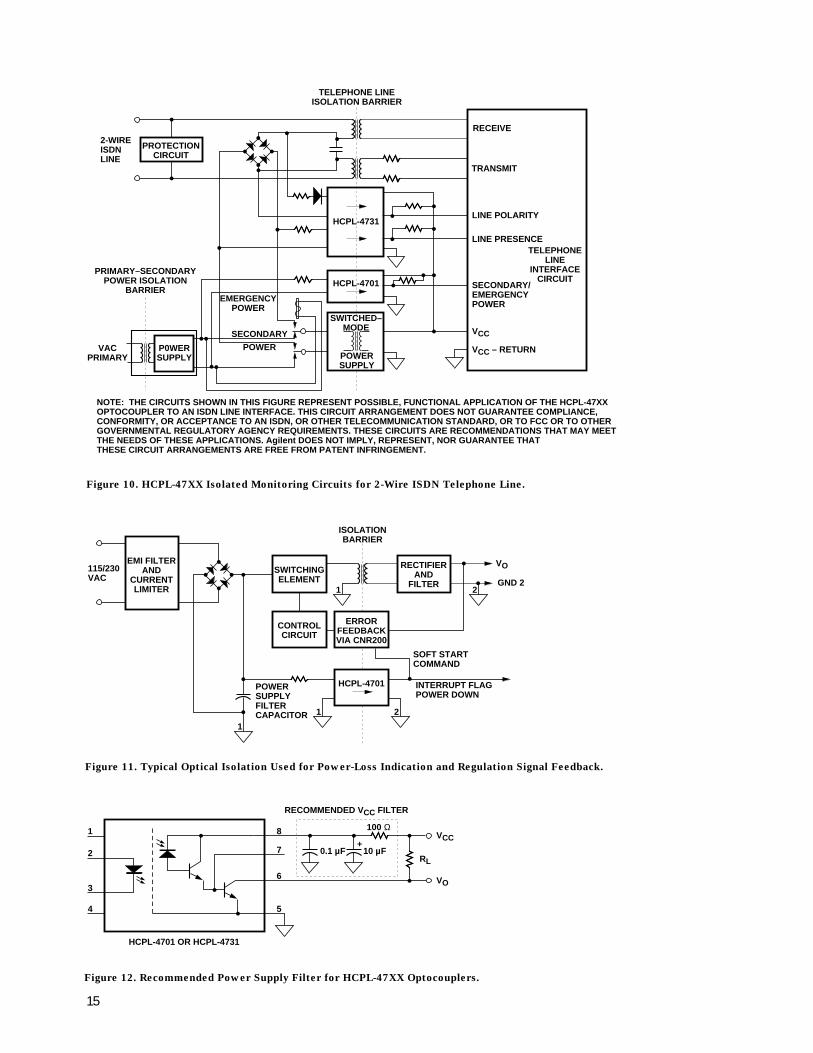
supplied-power sensing. Inparticular, Integrated ServicesDigital Network (ISDN) applica-tions, as illustrated in Figure 10,can severely restrict the inputpower that an optocoupler inter-face circuit can use (approxi-mately 3 mW). Figure 10 showsthree isolated signals that can beserved by the small input LEDcurrent of the HCPL-47XX dual-and single-channel optocouplers.Very low, total power dissipationoccurs with these series ofdevices.
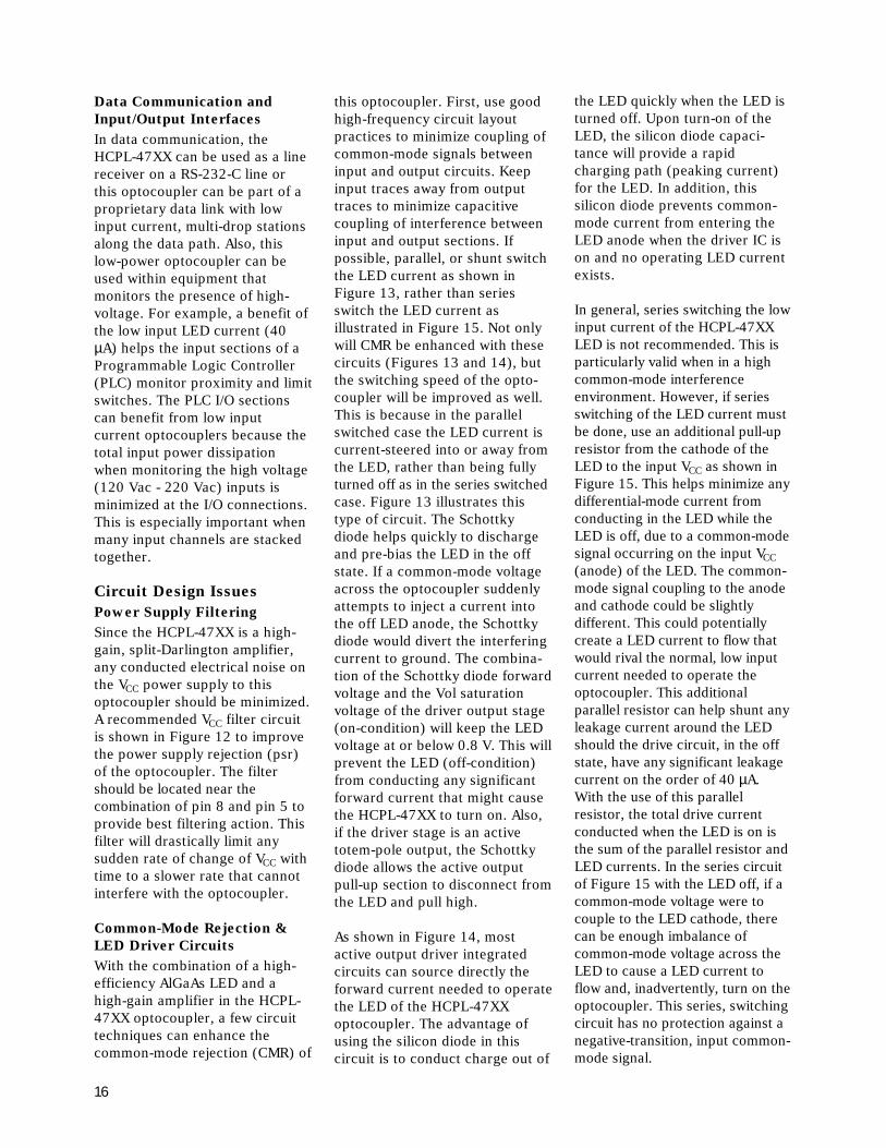
Switched-Mode PowerSuppliesWithin Switched-Mode PowerSupplies (SMPS) the less powerconsumed the better. Isolation formonitoring line power, regulationstatus, for use within a feedbackpath between primary andsecondary circuits or to externalcircuits are common applicationsfor optocouplers. Low-powerHCPL-47XX optocoupler can helpkeep higher energy conversionefficiency for the SMPS. The blockdiagram of Figure 11 shows wherelow-power isolation can be used.
Table 1. Typical HCPL-4701 Power Dissipation for 3 V and 5 V ApplicationsVCC = 3.3 Vdc VCC = 5 Vdc
(µW) IF = 40 µA IF = 500 µA IF = 40 µA IF = 500 µAPLED 50 625 50 625PVcc 65 330 100 500
PO-C[1] 20 10 25 20
PTOTAL[2] 135 µW 965 µW 175 µW 1,145 µW
Notes:1. RL of 11 kΩ open-collector (o-c) pull-up resistor was used for both 3.3 Vdc and 5 Vdc calculations.2. For typical total interface circuit power consumption in 3.3 Vdc application, add to PTOTAL approximately 80 µW for 40 µA
(1,025 µW for 500 µA) LED current-limiting resistor, and 960 µW for the 11 kΩ pull-up resistor power dissipations. Similarly, for 5Vdc applications, add to PTOTAL approximately 150 µW for 40 µA (1,875 µW for 500 µA) LED current-limiting resistor and 2,230µW for the 11 kΩ pull-up resistor power dissipations.
Power Dissipation
15
Figure 12. Recommended Power Supply Filter for HCPL-47XX Optocouplers.
RECOMMENDED VCC FILTER
8
0.1 µF
VCC
10 µF+
100 Ω
VO
RL7
6
5
1
2
3
4
HCPL-4701 OR HCPL-4731
Figure 10. HCPL-47XX Isolated Monitoring Circuits for 2-Wire ISDN Telephone Line.
Figure 11. Typical Optical Isolation Used for Power-Loss Indication and Regulation Signal Feedback.
115/230VAC
EMI FILTERAND
CURRENTLIMITER
ISOLATIONBARRIER
VO
GND 2
1
1 2
1 2
SOFT STARTCOMMAND
INTERRUPT FLAGPOWER DOWN
POWERSUPPLYFILTERCAPACITOR
SWITCHINGELEMENT
RECTIFIERAND
FILTER
CONTROLCIRCUIT
ERRORFEEDBACKVIA CNR200
HCPL-4701
2-WIREISDNLINE
PROTECTIONCIRCUIT
P0WERSUPPLY
SECONDARY
POWER
EMERGENCYPOWER
PRIMARY–SECONDARYPOWER ISOLATION
BARRIER
VACPRIMARY
TELEPHONE LINEISOLATION BARRIER
HCPL-4731
HCPL-4701
SWITCHED–MODE
POWERSUPPLY
RECEIVE
TRANSMIT
LINE POLARITY
LINE PRESENCE
SECONDARY/EMERGENCYPOWER
VCC
VCC – RETURN
TELEPHONELINE
INTERFACECIRCUIT
NOTE: THE CIRCUITS SHOWN IN THIS FIGURE REPRESENT POSSIBLE, FUNCTIONAL APPLICATION OF THE HCPL-47XX OPTOCOUPLER TO AN ISDN LINE INTERFACE. THIS CIRCUIT ARRANGEMENT DOES NOT GUARANTEE COMPLIANCE, CONFORMITY, OR ACCEPTANCE TO AN ISDN, OR OTHER TELECOMMUNICATION STANDARD, OR TO FCC OR TO OTHER GOVERNMENTAL REGULATORY AGENCY REQUIREMENTS. THESE CIRCUITS ARE RECOMMENDATIONS THAT MAY MEET THE NEEDS OF THESE APPLICATIONS. Agilent DOES NOT IMPLY, REPRESENT, NOR GUARANTEE THAT THESE CIRCUIT ARRANGEMENTS ARE FREE FROM PATENT INFRINGEMENT.
Data Communication andInput/Output InterfacesIn data communication, theHCPL-47XX can be used as a linereceiver on a RS-232-C line orthis optocoupler can be part of aproprietary data link with lowinput current, multi-drop stationsalong the data path. Also, thislow-power optocoupler can beused within equipment thatmonitors the presence of high-voltage. For example, a benefit ofthe low input LED current (40µA) helps the input sections of aProgrammable Logic Controller(PLC) monitor proximity and limitswitches. The PLC I/O sectionscan benefit from low inputcurrent optocouplers because thetotal input power dissipationwhen monitoring the high voltage(120 Vac - 220 Vac) inputs isminimized at the I/O connections.This is especially important whenmany input channels are stackedtogether.
Circuit Design IssuesPower Supply FilteringSince the HCPL-47XX is a high-gain, split-Darlington amplifier,any conducted electrical noise onthe VCC power supply to thisoptocoupler should be minimized.A recommended VCC filter circuitis shown in Figure 12 to improvethe power supply rejection (psr)of the optocoupler. The filtershould be located near thecombination of pin 8 and pin 5 toprovide best filtering action. Thisfilter will drastically limit anysudden rate of change of VCC withtime to a slower rate that cannotinterfere with the optocoupler.
Common-Mode Rejection &LED Driver CircuitsWith the combination of a high-efficiency AlGaAs LED and ahigh-gain amplifier in the HCPL-47XX optocoupler, a few circuittechniques can enhance thecommon-mode rejection (CMR) of
this optocoupler. First, use goodhigh-frequency circuit layoutpractices to minimize coupling ofcommon-mode signals betweeninput and output circuits. Keepinput traces away from outputtraces to minimize capacitivecoupling of interference betweeninput and output sections. Ifpossible, parallel, or shunt switchthe LED current as shown inFigure 13, rather than seriesswitch the LED current asillustrated in Figure 15. Not onlywill CMR be enhanced with thesecircuits (Figures 13 and 14), butthe switching speed of the opto-coupler will be improved as well.This is because in the parallelswitched case the LED current iscurrent-steered into or away fromthe LED, rather than being fullyturned off as in the series switchedcase. Figure 13 illustrates thistype of circuit. The Schottkydiode helps quickly to dischargeand pre-bias the LED in the offstate. If a common-mode voltageacross the optocoupler suddenlyattempts to inject a current intothe off LED anode, the Schottkydiode would divert the interferingcurrent to ground. The combina-tion of the Schottky diode forwardvoltage and the Vol saturationvoltage of the driver output stage(on-condition) will keep the LEDvoltage at or below 0.8 V. This willprevent the LED (off-condition)from conducting any significantforward current that might causethe HCPL-47XX to turn on. Also,if the driver stage is an activetotem-pole output, the Schottkydiode allows the active outputpull-up section to disconnect fromthe LED and pull high.
As shown in Figure 14, mostactive output driver integratedcircuits can source directly theforward current needed to operatethe LED of the HCPL-47XXoptocoupler. The advantage ofusing the silicon diode in thiscircuit is to conduct charge out of
the LED quickly when the LED isturned off. Upon turn-on of theLED, the silicon diode capaci-tance will provide a rapidcharging path (peaking current)for the LED. In addition, thissilicon diode prevents common-mode current from entering theLED anode when the driver IC ison and no operating LED currentexists.
In general, series switching the lowinput current of the HCPL-47XXLED is not recommended. This isparticularly valid when in a highcommon-mode interferenceenvironment. However, if seriesswitching of the LED current mustbe done, use an additional pull-upresistor from the cathode of theLED to the input VCC as shown inFigure 15. This helps minimize anydifferential-mode current fromconducting in the LED while theLED is off, due to a common-modesignal occurring on the input VCC(anode) of the LED. The common-mode signal coupling to the anodeand cathode could be slightlydifferent. This could potentiallycreate a LED current to flow thatwould rival the normal, low inputcurrent needed to operate theoptocoupler. This additionalparallel resistor can help shunt anyleakage current around the LEDshould the drive circuit, in the offstate, have any significant leakagecurrent on the order of 40 µA.With the use of this parallelresistor, the total drive currentconducted when the LED is on isthe sum of the parallel resistor andLED currents. In the series circuitof Figure 15 with the LED off, if acommon-mode voltage were tocouple to the LED cathode, therecan be enough imbalance ofcommon-mode voltage across theLED to cause a LED current toflow and, inadvertently, turn on theoptocoupler. This series, switchingcircuit has no protection against anegative-transition, input common-mode signal.
16
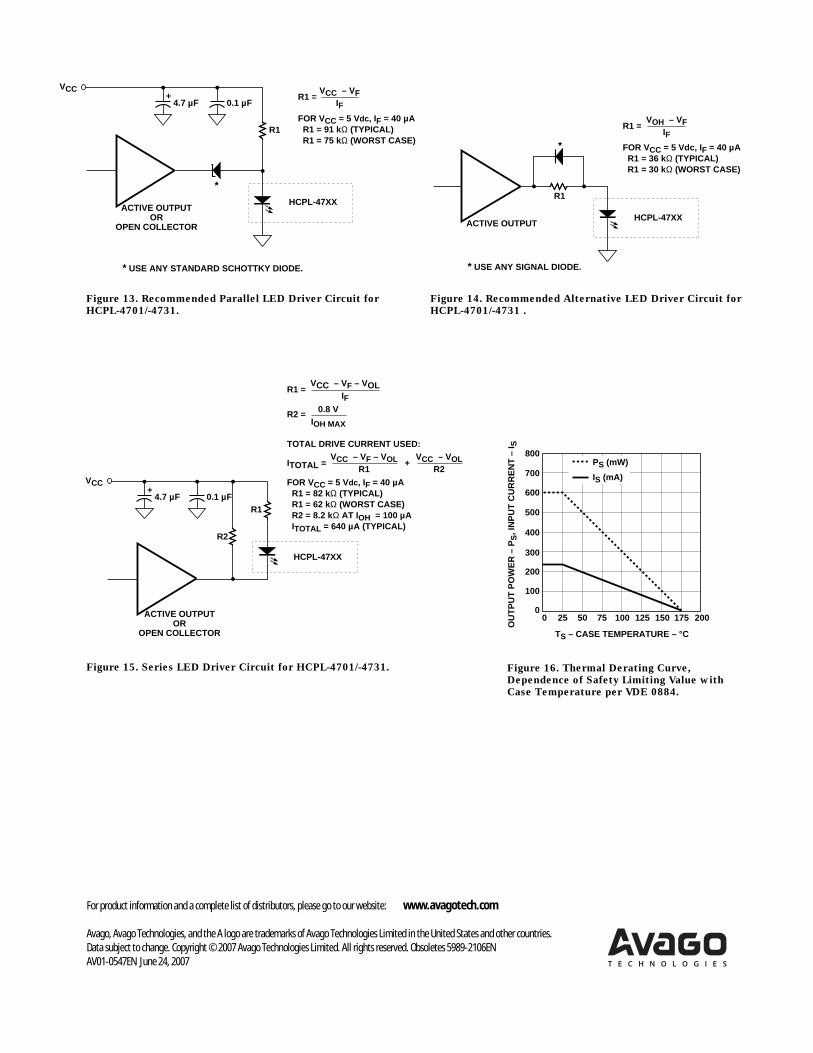
Figure 15. Series LED Driver Circuit for HCPL-4701/-4731.
OU
TP
UT
PO
WE
R –
PS
, IN
PU
T C
UR
RE
NT
– I S
00
TS – CASE TEMPERATURE – °C
20050
400
12525 75 100 150
600
800
200
100
300
500
700PS (mW)
IS (mA)
175
Figure 16. Thermal Derating Curve,Dependence of Safety Limiting Value withCase Temperature per VDE 0884.
4.7 µF
VCC
0.1 µF+
R1
HCPL-47XX
ACTIVE OUTPUTOR
OPEN COLLECTOR
R1 =VCC – VF – VOL
IF
FOR VCC = 5 Vdc, IF = 40 µA R1 = 82 kΩ (TYPICAL) R1 = 62 kΩ (WORST CASE) R2 = 8.2 kΩ AT IOH = 100 µA ITOTAL = 640 µA (TYPICAL)
R2
R2 = 0.8 VIOH MAX
ITOTAL =
TOTAL DRIVE CURRENT USED:
+VCC – VF – VOL
R1VCC – VOL
R2
Figure 13. Recommended Parallel LED Driver Circuit forHCPL-4701/-4731.
Figure 14. Recommended Alternative LED Driver Circuit forHCPL-4701/-4731 .
4.7 µF
VCC
0.1 µF+
R1
HCPL-47XXACTIVE OUTPUT
OROPEN COLLECTOR
*
* USE ANY STANDARD SCHOTTKY DIODE.
R1 =VCC – VF
IF
FOR VCC = 5 Vdc, IF = 40 µA R1 = 91 kΩ (TYPICAL) R1 = 75 kΩ (WORST CASE)
R1
HCPL-47XXACTIVE OUTPUT
*
* USE ANY SIGNAL DIODE.
R1 =VOH – VF
IF
FOR VCC = 5 Vdc, IF = 40 µA R1 = 36 kΩ (TYPICAL) R1 = 30 kΩ (WORST CASE)
For product information and a complete list of distributors, please go to our website: www.avagotech.com
Avago, Avago Technologies, and the A logo are trademarks of Avago Technologies Limited in the United States and other countries.Data subject to change. Copyright © 2007 Avago Technologies Limited. All rights reserved. Obsoletes 5989-2106ENAV01-0547EN June 24, 2007


![Data Sheet - RS Components Internationaldocs-europe.electrocomponents.com/webdocs/0ad5/0900766b80ad52… · NO HCPL-4661 HCPL-0661 1,000 50 YES HCPL-2602[1] 3 , 500 300 ... HCPL-2601/11/30/31,](https://img.pdfslide.net/doc/110x75/5ae874c47f8b9aee078f8e9c/data-sheet-rs-components-internationaldocs-no-hcpl-4661-hcpl-0661-1000-50.jpg)


![AV02-0940EN DS 6N137 29Mar2010 - Farnell element14 · NO HCPL-4661 HCPL-0661 1,000 50 YES HCPL-2602[1] 3, 500 300 ... HCPL-2601/11/30/31, HCPL-4661) 8-pin DIP Package with Gull Wing](https://img.pdfslide.net/doc/110x75/5ae874c47f8b9aee078f8e91/av02-0940en-ds-6n137-29mar2010-farnell-hcpl-4661-hcpl-0661-1000-50-yes-hcpl-26021.jpg)