Embed Size (px)
Citation preview
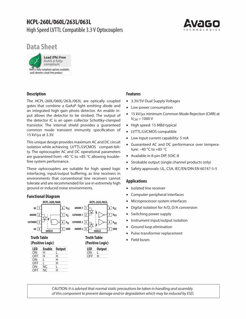
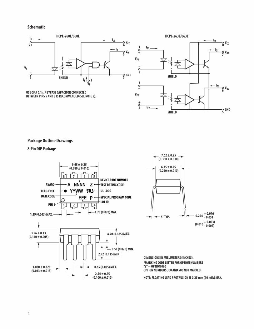
DescriptionThe HCPL-260L/060L/263L/063L are optically coupled gates that combine a GaAsP light emitting diode and an integrated high gain photo detector. An enable in-put allows the detector to be strobed. The output of the detector IC is an open collector Schottky-clamped transistor. The internal shield provides a guaranteed common mode transient immunity specification of 15 kV/µs at 3.3V.
This unique design provides maximum AC and DC circuit isolation while achieving LVTTL/LVCMOS compati-bili-ty. The optocoupler AC and DC operational parameters are guaranteed from –40 °C to +85 °C allowing trouble-free system performance.
These optocouplers are suitable for high speed logic interfacing, input/output buffering, as line receivers in environments that conventional line receivers cannot tolerate and are recommended for use in extremely high ground or induced noise environments.
Functional Diagram
HCPL-260L/060L/263L/063LHigh Speed LVTTL Compatible 3.3 V Optocouplers
Data Sheet Lead (Pb) FreeRoHS 6 fullycompliant
RoHS 6 fully compliant options available;-xxxE denotes a lead-free product
CAUTION: It is advised that normal static precautions be taken in handling and assembly of this component to prevent damage and/or degradation which may be induced by ESD.
Features• 3.3V/5V Dual Supply Voltages
• Low power consumption
• 15 kV/µs minimum Common Mode Rejection (CMR) at VCM = 1000 V
• High speed: 15 MBd typical
• LVTTL/LVCMOS compatible
• Low input current capability: 5 mA
• Guaranteed AC and DC performance over tempera-ture: –40 °C to +85 °C
• Available in 8-pin DIP, SOIC-8
• Strobable output (single channel products only)
• Safety approvals: UL, CSA, IEC/EN/DIN EN 60747-5-5
Applications• Isolated line receiver
• Computer-peripheral interfaces
• Microprocessor system interfaces
• Digital isolation for A/D, D/A conversion
• Switching power supply
• Instrument input/output isolation
• Ground loop elimination
• Pulse transformer replacement
• Field busesTruth Table(Positive Logic)
LED Enable OutputON H LOFF H HON L HOFF L HON NC LOFF NC H
Truth Table(Positive Logic)
LED OutputON LOFF H
1
2
3
4
8
7
6
5
CATHODE
ANODE
GND
V
VCC
O
1
2
3
4
8
7
6
5ANODE 2
CATHODE 2
CATHODE 1
ANODE 1
GND
V
VCC
O2
VE VO1
HCPL-260L/060L HCPL-263L/063L
NC
NCSHIELD SHIELD
2
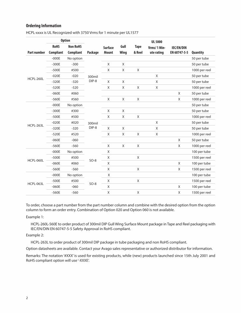
Ordering Information HCPL-xxxx is UL Recognized with 3750 Vrms for 1 minute per UL1577
Part number
Option
PackageSurface Mount
GullWing
Tape& Reel
UL 5000Vrms/ 1 Min-
ute ratingIEC/EN/DIN
EN 60747-5-5 QuantityRoHS
CompliantNon RoHSCompliant
HCPL-260L
-000E No option
300mil DIP-8
50 per tube
-300E -300 X X 50 per tube
-500E #500 X X X 1000 per reel
-020E -020 X 50 per tube
-320E -320 X X X 50 per tube
-520E -520 X X X X 1000 per reel
-060E #060 X 50 per tube
-560E #560 X X X X 1000 per reel
HCPL-263L
-000E No option
300mil DIP-8
50 per tube
-300E #300 X X 50 per tube
-500E #500 X X X 1000 per reel
-020E #020 X 50 per tube
-320E -320 X X X 50 per tube
-520E #520 X X X X 1000 per reel
-060E -060 X 50 per tube
-560E -560 X X X X 1000 per reel
HCPL-060L
-000E No option
SO-8
X 100 per tube
-500E #500 X X 1500 per reel
-060E #060 X X 100 per tube
-560E -560 X X X 1500 per reel
HCPL-063L
-000E No option
SO-8
X 100 per tube
-500E #500 X X 1500 per reel
-060E -060 X X 100 per tube
-560E -560 X X X 1500 per reel
To order, choose a part number from the part number column and combine with the desired option from the option column to form an order entry. Combination of Option 020 and Option 060 is not available.
Example 1:
HCPL-260L-560E to order product of 300mil DIP Gull Wing Surface Mount package in Tape and Reel packaging with IEC/EN/DIN EN 60747-5-5 Safety Approval in RoHS compliant.
Example 2:
HCPL-263L to order product of 300mil DIP package in tube packaging and non RoHS compliant.
Option datasheets are available. Contact your Avago sales representative or authorized distributor for information.
Remarks: The notation ‘#XXX’ is used for existing products, while (new) products launched since 15th July 2001 and RoHS compliant option will use ‘-XXXE‘.
3
Schematic
Package Outline Drawings
8-Pin DIP Package
SHIELD
8
6
5
2+
3
VF
USE OF A 0.1 µF BYPASS CAPACITOR CONNECTEDBETWEEN PINS 5 AND 8 IS RECOMMENDED (SEE NOTE 5).
–
IF ICC VCC
VO
GND
IO
VE
IE 7
HCPL-260L/060L
SHIELD
8
7+
2
VF1
–
IF1
ICC VCC
VO1IO1
1
SHIELD
6
5
–
4
VF2
+IF2
VO2
GND
IO23
HCPL-263L/063L
1.080 ± 0.320(0.043 ± 0.013)
2.54 ± 0.25(0.100 ± 0.010)
0.51 (0.020) MIN.
0.65 (0.025) MAX.
4.70 (0.185) MAX.
2.92 (0.115) MIN.
5° TYP. 0.254 + 0.076- 0.051
(0.010 + 0.003)- 0.002)
7.62 ± 0.25(0.300 ± 0.010)
6.35 ± 0.25(0.250 ± 0.010)
9.65 ± 0.25(0.380 ± 0.010)
1.78 (0.070) MAX.1.19 (0.047) MAX.
DIMENSIONS IN MILLIMETERS (INCHES).
5678
4321
*MARKING CODE LETTER FOR OPTION NUMBERS"V" = OPTION 060OPTION NUMBERS 300 AND 500 NOT MARKED.
NOTE: FLOATING LEAD PROTRUSION IS 0.25 mm (10 mils) MAX.
3.56 ± 0.13(0.140 ± 0.005)
EEE
NNNNYYWW
A•
TEST RATING CODEZ
P
DEVICE PART NUMBER
UL LOGO
SPECIAL PROGRAM CODE
LEAD-FREE
AVAGO
LOT IDDATE CODE
PIN 1
4
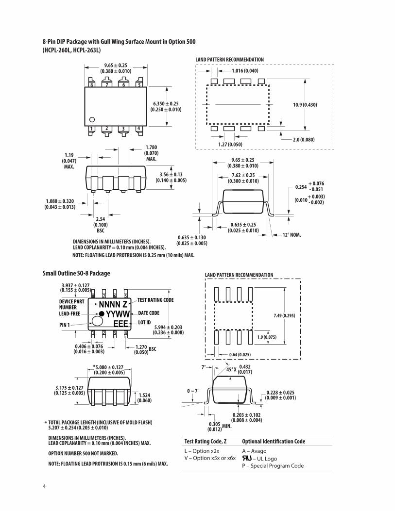
8-Pin DIP Package with Gull Wing Surface Mount in Option 500 (HCPL-260L, HCPL-263L)
Small Outline SO-8 Package
Test Rating Code, Z Optional Identification CodeL – Option x2xV – Option x5x or x6x
A – Avago – UL LogoP – Special Program Code
7.49 (0.295)
1.9 (0.075)
0.64 (0.025)
LAND PATTERN RECOMMENDATION
0.635 ± 0.25(0.025 ± 0.010)
12° NOM.
9.65 ± 0.25(0.380 ± 0.010)
0.635 ± 0.130(0.025 ± 0.005)
7.62 ± 0.25(0.300 ± 0.010)
5678
4321
9.65 ± 0.25(0.380 ± 0.010)
6.350 ± 0.25(0.250 ± 0.010)
1.016 (0.040)
1.27 (0.050)
10.9 (0.430)
2.0 (0.080)
LAND PATTERN RECOMMENDATION
1.080 ± 0.320(0.043 ± 0.013)
1.780(0.070)
MAX.1.19
(0.047)MAX.
2.54(0.100)
BSC
DIMENSIONS IN MILLIMETERS (INCHES).LEAD COPLANARITY = 0.10 mm (0.004 INCHES).
0.254 + 0.076- 0.051
(0.010+ 0.003)- 0.002)
NOTE: FLOATING LEAD PROTRUSION IS 0.25 mm (10 mils) MAX.
3.56 ± 0.13(0.140 ± 0.005)
8 7 6 5
43215.994 ± 0.203
(0.236 ± 0.008)
3.937 ± 0.127(0.155 ± 0.005)
0.406 ± 0.076(0.016 ± 0.003)
1.270(0.050)BSC
5.080 ± 0.127(0.200 ± 0.005)
3.175 ± 0.127(0.125 ± 0.005) 1.524
(0.060)
45° X 0.432(0.017)
0.228 ± 0.025(0.009 ± 0.001)
0.305(0.012)MIN.
TOTAL PACKAGE LENGTH (INCLUSIVE OF MOLD FLASH)5.207 ± 0.254 (0.205 ± 0.010)
DIMENSIONS IN MILLIMETERS (INCHES).LEAD COPLANARITY = 0.10 mm (0.004 INCHES) MAX.
OPTION NUMBER 500 NOT MARKED.
NOTE: FLOATING LEAD PROTRUSION IS 0.15 mm (6 mils) MAX.
0.203 ± 0.102(0.008 ± 0.004)
7°
0 ~ 7°
*
*
YYWW•NNNN Z
EEE
TEST RATING CODEDEVICE PART NUMBERLEAD-FREE
LOT ID
DATE CODE
PIN 1
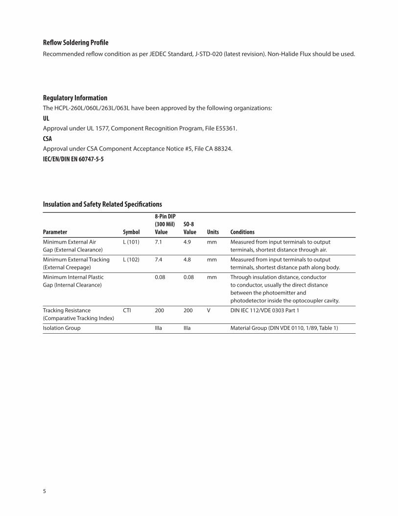
5
Insulation and Safety Related Specifications 8-Pin DIP (300 Mil) SO-8 Parameter Symbol Value Value Units ConditionsMinimum External Air L (101) 7.1 4.9 mm Measured from input terminals to output Gap (External Clearance) terminals, shortest distance through air.
Minimum External Tracking L (102) 7.4 4.8 mm Measured from input terminals to output (External Creepage) terminals, shortest distance path along body.
Minimum Internal Plastic 0.08 0.08 mm Through insulation distance, conductor Gap (Internal Clearance) to conductor, usually the direct distance between the photoemitter and photodetector inside the optocoupler cavity.
Tracking Resistance CTI 200 200 V DIN IEC 112/VDE 0303 Part 1 (Comparative Tracking Index)
Isolation Group IIIa IIIa Material Group (DIN VDE 0110, 1/89, Table 1)
Regulatory InformationThe HCPL-260L/060L/263L/063L have been approved by the following organizations:
ULApproval under UL 1577, Component Recognition Program, File E55361.
CSAApproval under CSA Component Acceptance Notice #5, File CA 88324.
IEC/EN/DIN EN 60747-5-5
Reflow Soldering ProfileRecommended reflow condition as per JEDEC Standard, J-STD-020 (latest revision). Non-Halide Flux should be used.
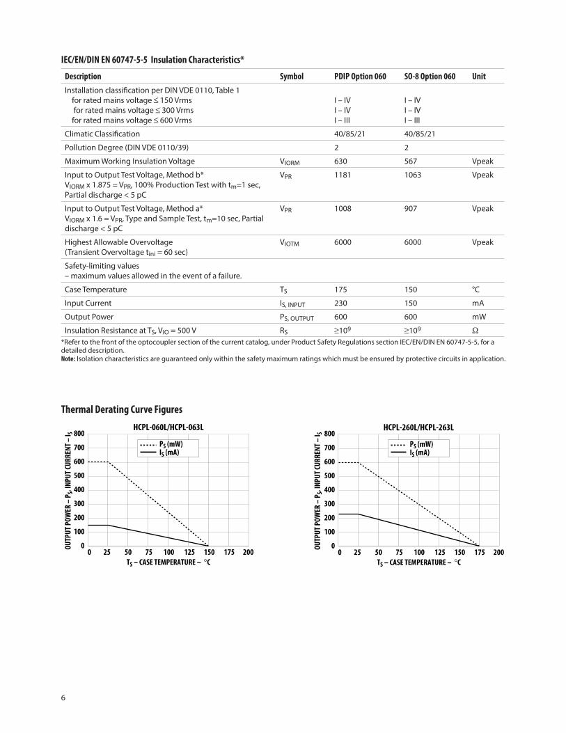
6
Thermal Derating Curve Figures
IEC/EN/DIN EN 60747-5-5 Insulation Characteristics*
Description Symbol PDIP Option 060 SO-8 Option 060 UnitInstallation classification per DIN VDE 0110, Table 1 for rated mains voltage ≤ 150 Vrms for rated mains voltage ≤ 300 Vrms for rated mains voltage ≤ 600 Vrms
I – IVI – IVI – III
I – IVI – IVI – III
Climatic Classification 40/85/21 40/85/21
Pollution Degree (DIN VDE 0110/39) 2 2
Maximum Working Insulation Voltage VIORM 630 567 Vpeak
Input to Output Test Voltage, Method b*VIORM x 1.875 = VPR, 100% Production Test with tm=1 sec, Partial discharge < 5 pC
VPR 1181 1063 Vpeak
Input to Output Test Voltage, Method a*VIORM x 1.6 = VPR, Type and Sample Test, tm=10 sec, Partial discharge < 5 pC
VPR 1008 907 Vpeak
Highest Allowable Overvoltage (Transient Overvoltage tini = 60 sec)
VIOTM 6000 6000 Vpeak
Safety-limiting values – maximum values allowed in the event of a failure.
Case Temperature TS 175 150 °C
Input Current IS, INPUT 230 150 mA
Output Power PS, OUTPUT 600 600 mW
Insulation Resistance at TS, VIO = 500 V RS ≥109 ≥109 W*Refer to the front of the optocoupler section of the current catalog, under Product Safety Regulations section IEC/EN/DIN EN 60747-5-5, for a detailed description. Note: Isolation characteristics are guaranteed only within the safety maximum ratings which must be ensured by protective circuits in application.
OUTP
UT P
OWER
– P
S, IN
PUT C
URRE
NT –
I S
00
TS – CASE TEMPERATURE – °C
HCPL-060L/HCPL-063L
200
700
400
25
800
50 75 100
200
150 175
PS (mW)IS (mA)
125
100
300
600
500
OUTP
UT P
OWER
– P
S, IN
PUT C
URRE
NT –
I S
00
TS – CASE TEMPERATURE – °C200
700
400
25
800
50 75 100
200
150 175
PS (mW)IS (mA)
125
100
300
600
500
HCPL-260L/HCPL-263L
7
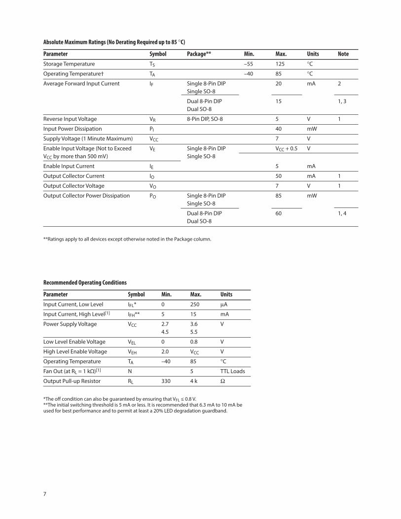
Absolute Maximum Ratings (No Derating Required up to 85 °C)
Parameter Symbol Package** Min. Max. Units NoteStorage Temperature TS –55 125 °C
Operating Temperature† TA –40 85 °C
Average Forward Input Current IF Single 8-Pin DIP 20 mA 2 Single SO-8
Dual 8-Pin DIP 15 1, 3 Dual SO-8
Reverse Input Voltage VR 8-Pin DIP, SO-8 5 V 1
Input Power Dissipation PI 40 mW
Supply Voltage (1 Minute Maximum) VCC 7 V
Enable Input Voltage (Not to Exceed VE Single 8-Pin DIP VCC + 0.5 V VCC by more than 500 mV) Single SO-8
Enable Input Current IE 5 mA
Output Collector Current IO 50 mA 1
Output Collector Voltage VO 7 V 1
Output Collector Power Dissipation PO Single 8-Pin DIP 85 mW Single SO-8
Dual 8-Pin DIP 60 1, 4 Dual SO-8
**Ratings apply to all devices except otherwise noted in the Package column.
Recommended Operating Conditions
Parameter Symbol Min. Max. UnitsInput Current, Low Level IFL* 0 250 µA
Input Current, High Level[1] IFH** 5 15 mA
Power Supply Voltage VCC 2.7 3.6 V 4.5 5.5
Low Level Enable Voltage VEL 0 0.8 V
High Level Enable Voltage VEH 2.0 VCC V
Operating Temperature TA –40 85 °C
Fan Out (at RL = 1 kΩ)[1] N 5 TTL Loads
Output Pull-up Resistor RL 330 4 k W
*The off condition can also be guaranteed by ensuring that VFL ≤ 0.8 V. **The initial switching threshold is 5 mA or less. It is recommended that 6.3 mA to 10 mA be used for best performance and to permit at least a 20% LED degradation guardband.
8
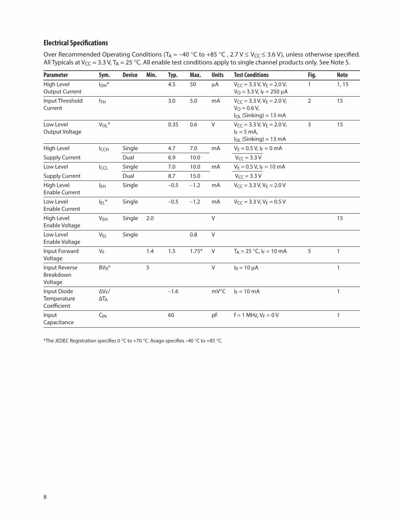
Electrical SpecificationsOver Recommended Operating Conditions (TA = –40 °C to +85 °C , 2.7 V ≤ VCC ≤ 3.6 V), unless otherwise specified. All Typicals at VCC = 3.3 V, TA = 25 °C. All enable test conditions apply to single channel products only. See Note 5.
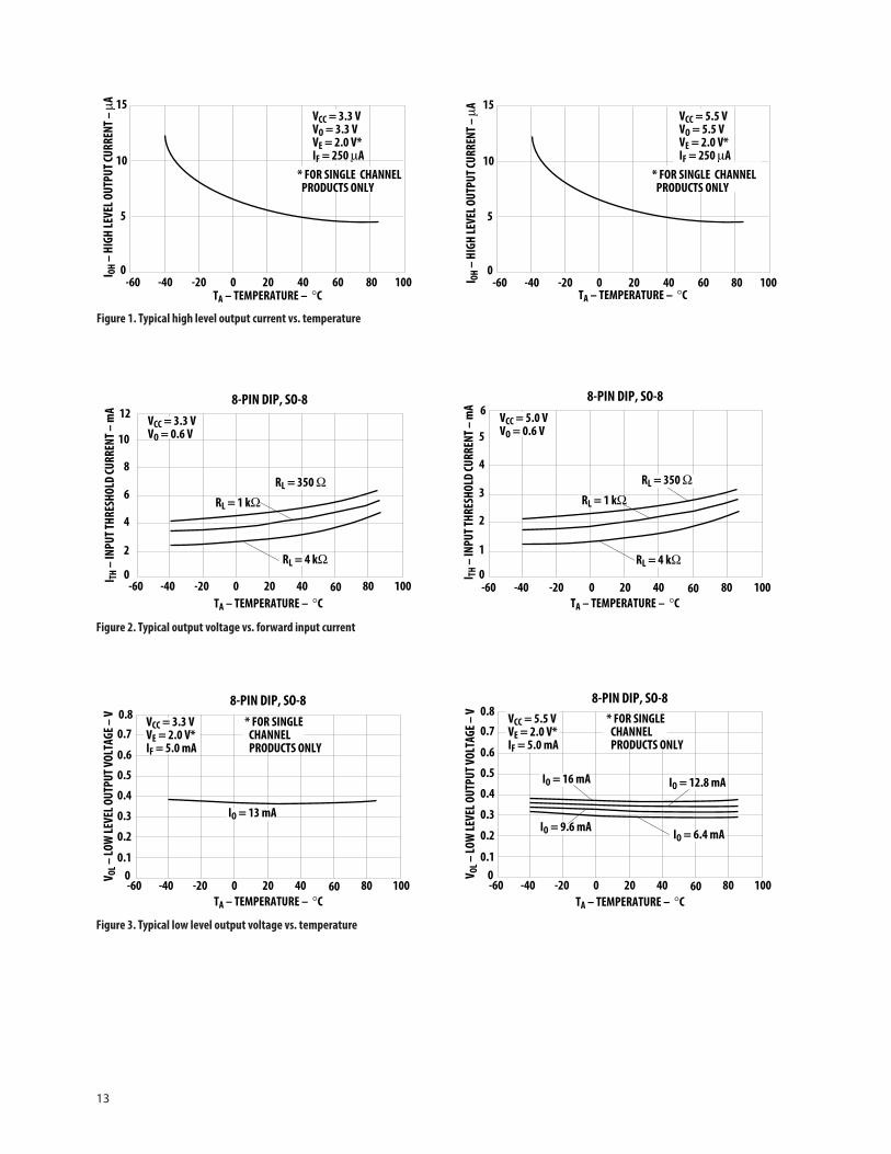
Parameter Sym. Device Min. Typ. Max. Units Test Conditions Fig. NoteHigh Level IOH* 4.5 50 µA VCC = 3.3 V, VE = 2.0 V, 1 1, 15 Output Current VO = 3.3 V, IF = 250 µA
Input Threshold ITH 3.0 5.0 mA VCC = 3.3 V, VE = 2.0 V, 2 15 Current VO = 0.6 V, IOL (Sinking) = 13 mA
Low Level VOL* 0.35 0.6 V VCC = 3.3 V, VE = 2.0 V, 3 15 Output Voltage IF = 5 mA, IOL (Sinking) = 13 mA
High Level ICCH Single 4.7 7.0 mA VE = 0.5 V, IF = 0 mA
Supply Current Dual 6.9 10.0 VCC = 3.3 V
Low Level ICCL Single 7.0 10.0 mA VE = 0.5 V, IF = 10 mA
Supply Current Dual 8.7 15.0 VCC = 3.3 V
High Level IEH Single –0.5 –1.2 mA VCC = 3.3 V, VE = 2.0 V Enable Current
Low Level IEL* Single –0.5 –1.2 mA VCC = 3.3 V, VE = 0.5 V Enable Current
High Level VEH Single 2.0 V 15 Enable Voltage
Low Level VEL Single 0.8 V Enable Voltage
Input Forward VF 1.4 1.5 1.75* V TA = 25 °C, IF = 10 mA 5 1 Voltage
Input Reverse BVR* 5 V IR = 10 µA 1 Breakdown Voltage
Input Diode ∆VF/ –1.6 mV°C IF = 10 mA 1 Temperature ∆TA Coefficient
Input CIN 60 pF f = 1 MHz, VF = 0 V 1 Capacitance
*The JEDEC Registration specifies 0 °C to +70 °C. Avago specifies –40 °C to +85 °C.
9
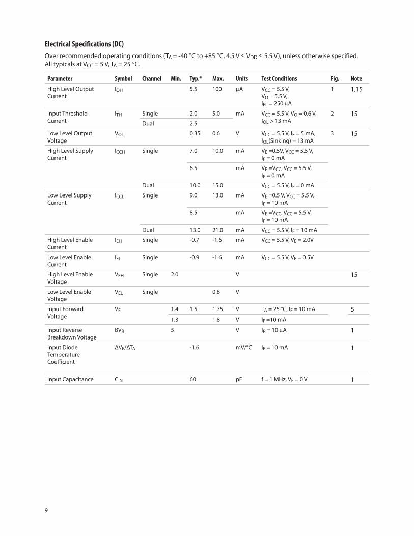
Electrical Specifications (DC)Over recommended operating conditions (TA = -40 °C to +85 °C, 4.5 V ≤ VDD ≤ 5.5 V), unless otherwise specified. All typicals at VCC = 5 V, TA = 25 °C.
Parameter Symbol Channel Min. Typ.* Max. Units Test Conditions Fig. NoteHigh Level Output Current
IOH 5.5 100 µA VCC = 5.5 V, VO = 5.5 V, IFL = 250 µA
1 1,15
Input ThresholdCurrent
ITH Single 2.0 5.0 mA VCC = 5.5 V, VO = 0.6 V, IOL > 13 mA
2 15Dual 2.5
Low Level OutputVoltage
VOL 0.35 0.6 V VCC = 5.5 V, IF = 5 mA, IOL(Sinking) = 13 mA
3 15
High Level SupplyCurrent
ICCH Single 7.0 10.0 mA VE =0.5V, VCC = 5.5 V, IF = 0 mA
6.5 mA VE =VCC, VCC = 5.5 V, IF = 0 mA
Dual 10.0 15.0 VCC = 5.5 V, IF = 0 mA
Low Level SupplyCurrent
ICCL Single 9.0 13.0 mA VE =0.5 V, VCC = 5.5 V, IF = 10 mA
8.5 mA VE =VCC, VCC = 5.5 V, IF = 10 mA
Dual 13.0 21.0 mA VCC = 5.5 V, IF = 10 mA
High Level EnableCurrent
IEH Single -0.7 -1.6 mA VCC = 5.5 V, VE = 2.0V
Low Level EnableCurrent
IEL Single -0.9 -1.6 mA VCC = 5.5 V, VE = 0.5V
High Level EnableVoltage
VEH Single 2.0 V 15
Low Level EnableVoltage
VEL Single 0.8 V
Input ForwardVoltage
VF 1.4 1.5 1.75 V TA = 25 °C, IF = 10 mA 51.3 1.8 V IF =10 mA
Input ReverseBreakdown Voltage
BVR 5 V IR = 10 µA 1
Input DiodeTemperatureCoefficient
ΔVF/ΔTA -1.6 mV/°C IF = 10 mA 1
Input Capacitance CIN 60 pF f = 1 MHz, VF = 0 V 1
10
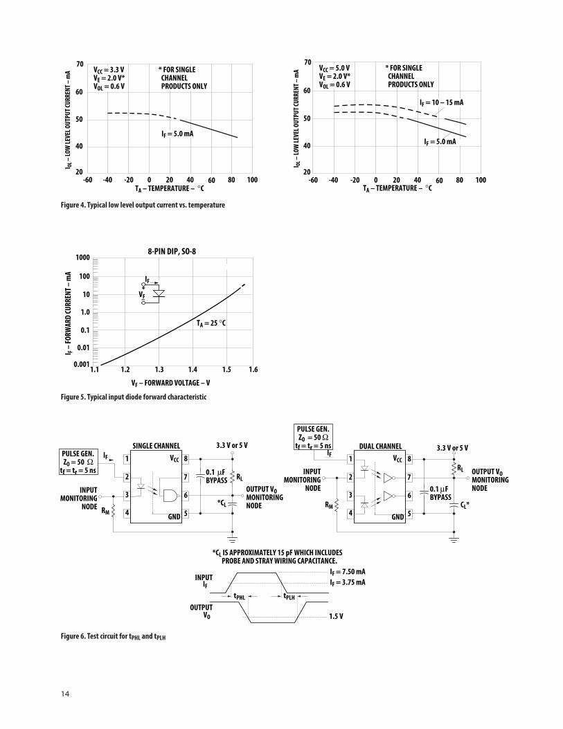
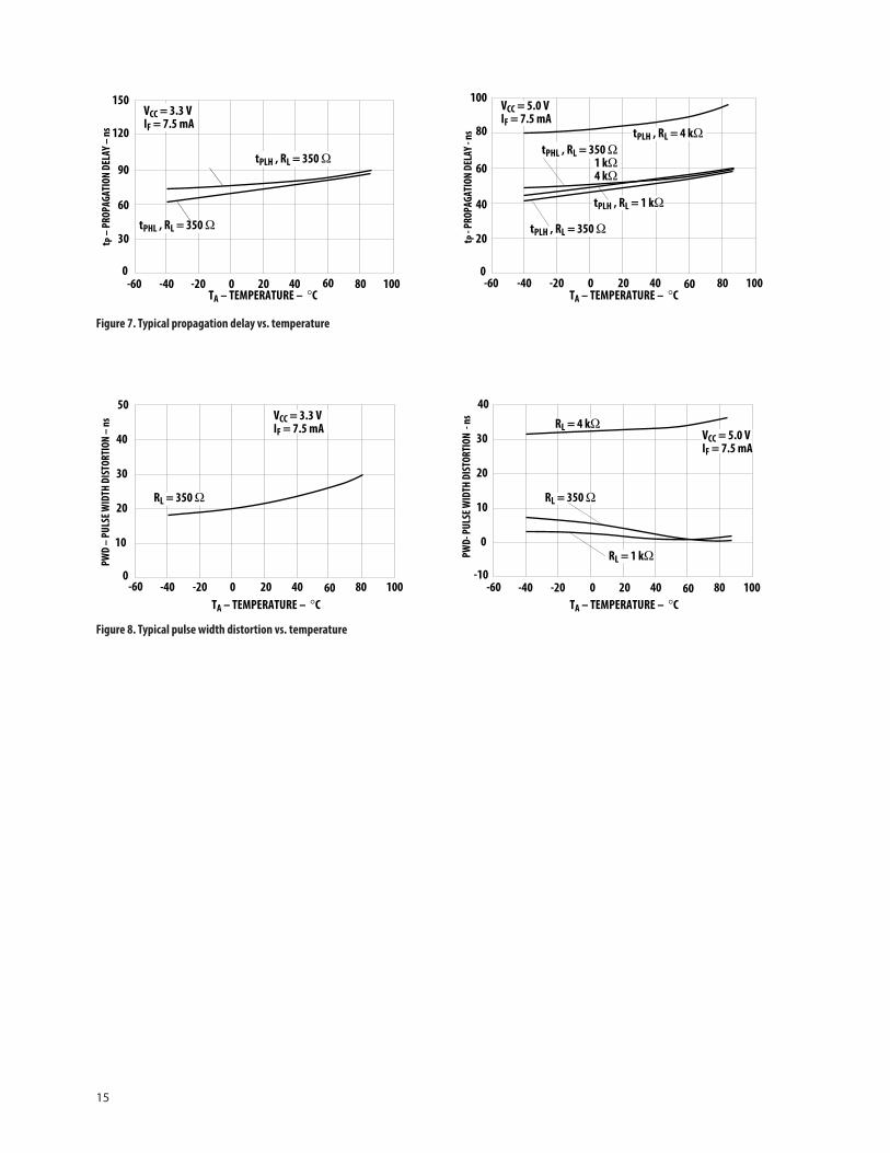
Switching SpecificationsOver Recommended Operating Conditions (TA = –40 °C to +85 °C, 2.7 V ≤ VCC ≤ 3.6 V), IF = 7.5 mA, unless otherwise specified. All Typicals at TA = 25 °C, VCC = 3.3 V.
Parameter Symbol Min. Typ. Max. Units Test Conditions Fig. NotePropagation DelayTime to High OutputLevel
tPLH 90 ns RL = 350 WCL = 15 pF
6, 7 1, 6, 15
Propagation DelayTime to Low OutputLevel
tPHL 75 ns RL = 350 WCL = 15 pF
1, 7, 15
Pulse Width Distortion
|tPHL – tPLH| 25 ns RL = 350 WCL = 15 pF
8 9, 15
Propagation DelaySkew
tPSK 40 ns RL = 350 WCL = 15 pF
8, 9, 15
Output Rise Time(10-90%)
tr 45 ns RL = 350 WCL = 15 pF
1, 15
Output Fall Time(90-10%)
tf 20 ns RL = 350 W CL = 15 pF
1, 15
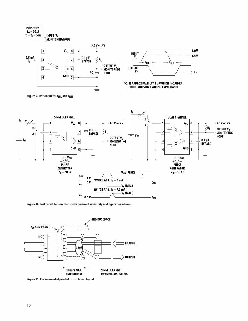
Propagation DelayTime of Enable fromVEH to VEL
tELH 45 ns RL = 350 W,CL = 15 pF,VEL = 0 V, VEH = 3 V
9 10
Propagation DelayTime of Enable fromVEL to VEH
tEHL 30 ns RL = 350 W,CL = 15 pF,VEL = 0 V, VEH = 3 V
9 11
11
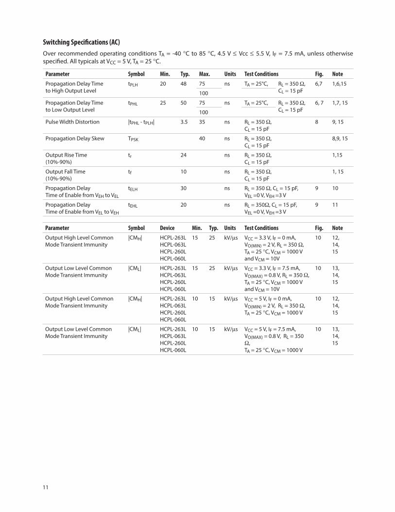
Parameter Symbol Device Min. Typ. Units Test Conditions Fig. NoteOutput High Level Common Mode Transient Immunity
|CMH| HCPL-263LHCPL-063LHCPL-260LHCPL-060L
15 25 kV/µs VCC = 3.3 V, IF = 0 mA,VO(MIN) = 2 V, RL = 350 W,TA = 25 °C, VCM = 1000 V and VCM = 10V
10 12,14,15
Output Low Level Common Mode Transient Immunity
|CML| HCPL-263LHCPL-063LHCPL-260LHCPL-060L
15 25 kV/µs VCC = 3.3 V, IF = 7.5 mA,VO(MAX) = 0.8 V, RL = 350 W,TA = 25 °C, VCM = 1000 V and VCM = 10V
10 13,14,15
Output High Level Common Mode Transient Immunity
|CMH| HCPL-263LHCPL-063LHCPL-260LHCPL-060L
10 15 kV/µs VCC = 5 V, IF = 0 mA,VO(MIN) = 2 V, RL = 350 W,TA = 25 °C, VCM = 1000 V
10 12,14,15
Output Low Level Common Mode Transient Immunity
|CML| HCPL-263LHCPL-063LHCPL-260LHCPL-060L
10 15 kV/µs VCC = 5 V, IF = 7.5 mA,VO(MAX) = 0.8 V, RL = 350 W,TA = 25 °C, VCM = 1000 V
10 13,14,15
Switching Specifications (AC)Over recommended operating conditions TA = -40 °C to 85 °C, 4.5 V ≤ Vcc ≤ 5.5 V, IF = 7.5 mA, unless otherwise specified. All typicals at VCC = 5 V, TA = 25 °C.
Parameter Symbol Min. Typ. Max. Units Test Conditions Fig. NotePropagation Delay Timeto High Output Level
tPLH 20 48 75 ns TA = 25°C, RL = 350 W, CL = 15 pF
6,7 1,6,15
100
Propagation Delay Time to Low Output Level
tPHL 25 50 75 ns TA = 25°C, RL = 350 W, CL = 15 pF
6, 7 1,7, 15
100
Pulse Width Distortion |tPHL - tPLH| 3.5 35 ns RL = 350 W,CL = 15 pF
8 9, 15
Propagation Delay Skew TPSK 40 ns RL = 350 W,CL = 15 pF
8,9, 15
Output Rise Time(10%-90%)
tr 24 ns RL = 350 W,CL = 15 pF
1,15
Output Fall Time(10%-90%)
tf 10 ns RL = 350 W,CL = 15 pF
1, 15
Propagation Delay Time of Enable from VEH to VEL
tELH 30 ns RL = 350 W, CL = 15 pF, VEL =0 V, VEH =3 V
9 10
Propagation Delay Time of Enable from VEL to VEH
tEHL 20 ns RL = 350W, CL = 15 pF, VEL =0 V, VEH =3 V
9 11
12
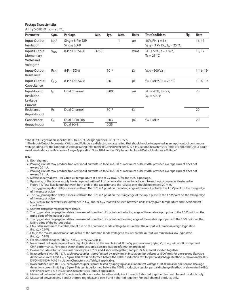
Package Characteristics All Typicals at TA = 25 °C.Parameter Sym. Package Min. Typ. Max. Units Test Conditions Fig. NoteInput-Output II-O* Single 8-Pin DIP 1 µA 45% RH, t = 5 s, 16, 17 Insulation Single SO-8 VI-O = 3 kV DC, TA = 25 °C
Input-Output VISO 8-Pin DIP, SO-8 3750 Vrms RH ≤ 50%, t = 1 min, 16, 17 Momentary TA = 25 °C Withstand Voltage**
Input-Output RI-O 8-Pin, SO-8 1012 W VI-O =500 Vdc 1, 16, 19 Resistance
Input-Output CI-O 8-Pin DIP, SO-8 0.6 pF f = 1 MHz, TA = 25 °C 1, 16, 19 Capacitance
Input-Input II-I Dual Channel 0.005 µA RH ≤ 45%, t = 5 s, 20 Insulation VI-I = 500 V Leakage Current Resistance RI-I Dual Channel 1011 W 20 (Input-Input)
Capacitance CI-I Dual 8-Pin Dip 0.03 pG f = 1 MHz 20 (Input-Input) Dual SO-8 0.25
*The JEDEC Registration specifies 0 °C to +70 °C. Avago specifies –40 °C to +85 °C. **The Input-Output Momentary Withstand Voltage is a dielectric voltage rating that should not be interpreted as an input-output continuous voltage rating. For the continuous voltage rating refer to the IEC/EN/DIN EN 60747-5-5 Insulation Characteristics Table (if applicable), your equip-ment level safety specification or Avago Application Note 1074 entitled "Optocoupler Input-Output Endurance Voltage."
Notes: 1. Each channel. 2. Peaking circuits may produce transient input currents up to 50 mA, 50 ns maximum pulse width, provided average current does not
exceed 20 mA. 3. Peaking circuits may produce transient input currents up to 50 mA, 50 ns maximum pulse width, provided average current does not
exceed 15 mA. 4. Derate linearly above +80˚C free-air temperature at a rate of 2.7 mW/˚C for the SOIC-8 package. 5. Bypassing of the power supply line is required, with a 0.1 µF ceramic disc capacitor adjacent to each optocoupler as illustrated in
Figure 11. Total lead length between both ends of the capacitor and the isolator pins should not exceed 20 mm. 6. The tPLH propagation delay is measured from the 3.75 mA point on the falling edge of the input pulse to the 1.5 V point on the rising edge
of the output pulse. 7. The tPHL propagation delay is measured from the 3.75 mA point on the rising edge of the input pulse to the 1.5 V point on the falling edge
of the output pulse. 8. tPSK is equal to the worst case difference in tPHL and/or tPLH that will be seen between units at any given temperature and specified test
conditions. 9. See test circuit for measurement details. 10. The tELH enable propagation delay is measured from the 1.5 V point on the falling edge of the enable input pulse to the 1.5 V point on the
rising edge of the output pulse. 11. The tEHL enable propagation delay is measured from the 1.5 V point on the rising edge of the enable input pulse to the 1.5 V point on the
falling edge of the output pulse. 12. CMH is the maximum tolerable rate of rise on the common mode voltage to assure that the output will remain in a high logic state
(i.e., Vo > 2.0 V). 13. CML is the maximum tolerable rate of fall of the common mode voltage to assure that the output will remain in a low logic state
(i.e., Vo < 0.8 V). 14. For sinusoidal voltages, (|dVCM | / dt)max = πfCMVCM (p-p). 15. No external pull up is required for a high logic state on the enable input. If the VE pin is not used, tying VE to VCC will result in improved
CMR performance. For single channel products only. See application information provided. 16. Device considered a two-terminal device: pins 1, 2, 3, and 4 shorted together, and pins 5, 6, 7, and 8 shorted together. 17. In accordance with UL 1577, each optocoupler is proof tested by applying an insulation test voltage ≥ 4500 Vrms for one second (leakage
detection current limit, II-O ≤ 5 µA). This test is performed before the 100% production test for partial discharge (Method b) shown in the IEC/EN/DIN EN 60747-5-5 Insulation Characteristics Table, if applicable.
18. In accordance with UL 1577, each optocoupler is proof tested by applying an insulation test voltage ≥ 6000 Vrms for one second (leakage detection current limit, II-O ≤ 5 µA). This test is performed before the 100% production test for partial discharge (Method b) shown in the IEC/EN/DIN EN 60747-5-5 Insulation Characteristics Table, if applicable.
19. Measured between the LED anode and cathode shorted together and pins 5 through 8 shorted together. For dual channel products only. 20. Measured between pins 1 and 2 shorted together, and pins 3 and 4 shorted together. For dual channel products only.
13
I OH –
HIG
H LE
VEL O
UTPU
T CUR
RENT
– µ
A
-600
TA – TEMPERATURE – °C100
10
15
-20
5
20
VCC = 3.3 VVO = 3.3 VVE = 2.0 V*IF = 250 µA
60-40 0 40 80
* FOR SINGLE CHANNEL PRODUCTS ONLY
I OH –
HIG
H LE
VEL O
UTPU
T CUR
RENT
– µ
A
-600
100
10
15
-20
5
20 60-40 0 40 80
VCC = 3.3 VVO = 0.6 V
12
6
-60 -20 20 60 100
4
80400-400I TH
– IN
PUT T
HRES
HOLD
CURR
ENT –
mA
RL = 350 Ω
2
8
10
RL = 1 kΩ
RL = 4 kΩ
8-PIN DIP, SO-8VCC = 5.0 VVO = 0.6 V
6
3
-60 -20 20 60 100
2
80400-400
1
4
5
8-PIN DIP, SO-8
0.8
0.4
-60 -20 20 60 100
0.2
80400-400V O
L – LO
W LE
VEL O
UTPU
T VOL
TAGE
– V
IO = 13 mA
0.1
0.5
0.7
8-PIN DIP, SO-8VCC = 3.3 VVE = 2.0 V*IF = 5.0 mA
0.3
0.6
* FOR SINGLE CHANNEL PRODUCTS ONLY
0.8
0.4
-60 -20 20 60 100
0.2
80400-400
IO = 16 mA
0.1
0.5
0.7
IO = 6.4 mA
VCC = 5.5 VVE = 2.0 V*IF = 5.0 mA
0.3
0.6
IO = 12.8 mA
IO = 9.6 mA
* FOR SINGLE CHANNEL PRODUCTS ONLY
* FOR SINGLE CHANNEL PRODUCTS ONLY
TA – TEMPERATURE – °C
TA – TEMPERATURE – °C
I TH –
INPU
T THR
ESHO
LD CU
RREN
T – m
A
TA – TEMPERATURE – °C
RL = 350 ΩRL = 1 kΩ
RL = 4 kΩ
TA – TEMPERATURE – °C
V OL –
LOW
LEVE
L OUT
PUT V
OLTA
GE –
V
8-PIN DIP, SO-8
TA – TEMPERATURE – °C
VCC = 5.5 VVO = 5.5 VVE = 2.0 V*IF = 250 µA
Figure 1. Typical high level output current vs. temperature
Figure 3. Typical low level output voltage vs. temperature
Figure 2. Typical output voltage vs. forward input current
14
Figure 6. Test circuit for tPHL and tPLH
Figure 5. Typical input diode forward characteristic
Figure 4. Typical low level output current vs. temperature
I F –
FORW
ARD
CURR
ENT –
mA
1.10.001
1.0
1000
1.3
0.01
1.51.2 1.4
0.1TA = 25 °C
10
100
8-PIN DIP, SO-8
1.6
+
–
IF
VF
VCC = 3.3 VVE = 2.0 V*VOL = 0.6 V
70
60
-60 -20 20 60 100
50
80400-4020
I OL –
LOW
LEVE
L OUT
PUT C
URRE
NT –
mA
40IF = 5.0 mA
* FOR SINGLE CHANNEL PRODUCTS ONLY
VCC = 5.0 VVE = 2.0 V*VOL = 0.6 V
70
60
-60 -20 20 60 100
50
80400-4020
40
IF = 10 – 15 mA
IF = 5.0 mA
* FOR SINGLE CHANNEL PRODUCTS ONLY
TA – TEMPERATURE – °C
I OL –
LOW
LEVE
L OUT
PUT C
URRE
NT –
mA
TA – TEMPERATURE – °C
VF – FORWARD VOLTAGE – V
OUTPUT VO MONITORING NODE
3.3 V or 5 V
7
5
6
8
2
3
4
1IF
RL
RM
VCC
0.1 µFBYPASS
*CL
GND
INPUTMONITORING
NODE
SINGLE CHANNEL
OUTPUT VO MONITORING NODE
3.3 V or 5 V
7
5
6
8
2
3
4
1
PULSE GEN.ZO = 50 Ω
tf = tr = 5 nsIF
RL
RM
VCC
0.1 µFBYPASS
CL*GND
INPUTMONITORING
NODE
DUAL CHANNEL
*CL IS APPROXIMATELY 15 pF WHICH INCLUDES PROBE AND STRAY WIRING CAPACITANCE.
1.5 V
tPHL tPLH
IFINPUT
VOOUTPUT
IF = 7.50 mA IF = 3.75 mA
PULSE GEN.ZO = 50 Ω
tf = tr = 5 ns
15
Figure 7. Typical propagation delay vs. temperature
Figure 8. Typical pulse width distortion vs. temperature
VCC = 3.3 VIF = 7.5 mA
150
120
-60 -20 20 60 100
90
80400-400
t P –
PRO
PAGA
TION
DEL
AY –
ns
60
30tPHL , RL = 350 Ω
tPLH , RL = 350 Ω
VCC = 5.0 VIF = 7.5 mA
100
80
-60 -20 20 60 100
60
80400-400
t P - P
ROPA
GATI
ON D
ELAY
- ns
40
20
tPLH , RL = 4 kΩ
tPLH , RL = 1 kΩ
tPLH , RL = 350 Ω
tPHL , RL = 350 Ω1 kΩ4 kΩ
40
30
-20 20 60 100
20
80400-40
PW
D- P
ULSE
WID
TH D
ISTO
RTIO
N - n
s
10
0
-60-10
VCC = 3.3 VIF = 7.5 mA
50
40
-20 20 60 100
30
80400-40
PWD
– PU
LSE W
IDTH
DIS
TORT
ION
– ns
20RL = 350 Ω
10
-600
TA – TEMPERATURE – °CTA – TEMPERATURE – °C
TA – TEMPERATURE – °C TA – TEMPERATURE – °C
RL = 1 kΩ
RL = 350 Ω
RL = 4 kΩVCC = 5.0 VIF = 7.5 mA
16
Figure 10. Test circuit for common mode transient immunity and typical waveforms
Figure 11. Recommended printed circuit board layout
Figure 9. Test circuit for tEHL and tELH
OUTPUT VO MONITORING NODE 1.5 V
tEHL tELH
VEINPUT
VOOUTPUT
3.0 V1.5 V
3.3 V or 5 V
7
5
6
8
2
3
4
1
I RL
VCC
0.1 µFBYPASS
*CL
*CL IS APPROXIMATELY 15 pF WHICH INCLUDES PROBE AND STRAY WIRING CAPACITANCE.
GND
7.5 mA
INPUT VEMONITORING NODE
3.3 V or 5 V
7
5
6
8
2
3
4
1 VCC
0.1 µFBYPASS
GND
OUTPUT VO MONITORING NODE
PULSEGENERATORZO = 50 Ω
+
IF
B
A
V
VCM–
RL
SINGLE CHANNEL
3.3 V or 5 V
7
5
6
8
2
3
4
1 VCC
0.1 µFBYPASS
GND
OUTPUT VO MONITORING NODE
PULSEGENERATORZO = 50 Ω
+
IF
B
A
VFF
VCM–
RL
DUAL CHANNEL
VO 0.5 V
VO (MIN.)5 V0 V SWITCH AT A: IF = 0 mA
SWITCH AT B: IF = 7.5 mA
VCM
CMH
CML
VO (MAX.)
VCM (PEAK)
VO
GND BUS (BACK)
VCC BUS (FRONT)
ENABLE0.1µF
10 mm MAX.(SEE NOTE 5)
OUTPUT
NC
NC
SINGLE CHANNELDEVICE ILLUSTRATED.
PULSE GEN.ZO = 50 Ω
tf = tr = 5 ns
F
FF
17
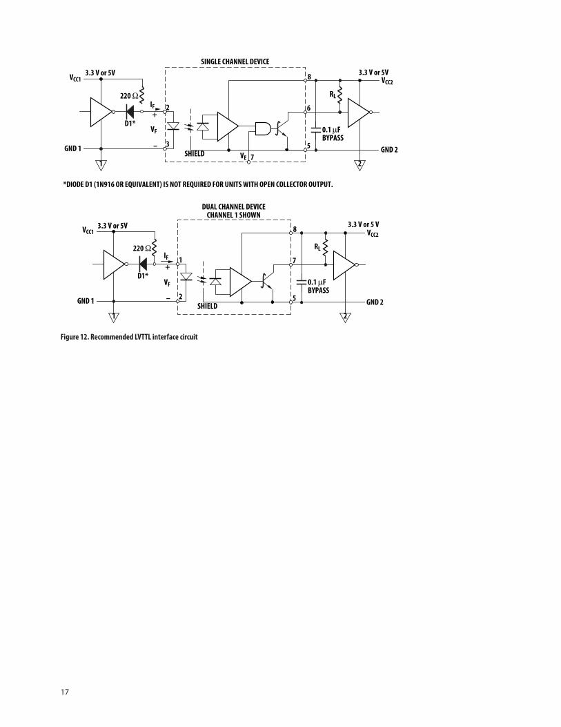
Figure 12. Recommended LVTTL interface circuit
*DIODE D1 (1N916 OR EQUIVALENT) IS NOT REQUIRED FOR UNITS WITH OPEN COLLECTOR OUTPUT.
VCC13.3 V or 5V
GND 1
D1*
IF
VF
SHIELD
SINGLE CHANNEL DEVICE
8
6
5
RL
0.1 µFBYPASS
2
3
+
–
3.3 V or 5V
GND 2
VCC2
2
220 Ω
17VE
VCC13.3 V or 5V
GND 1
D1*
SHIELD
DUAL CHANNEL DEVICECHANNEL 1 SHOWN
8
7
5
RL
0.1 µFBYPASS
1
2
+
–
3.3 V or 5 V
GND 2
VCC2
2
220 Ω
1
IF
VF
18
Figure 13. Recommended drive circuit for High-CMR
Figure 14. AC equivalent circuit
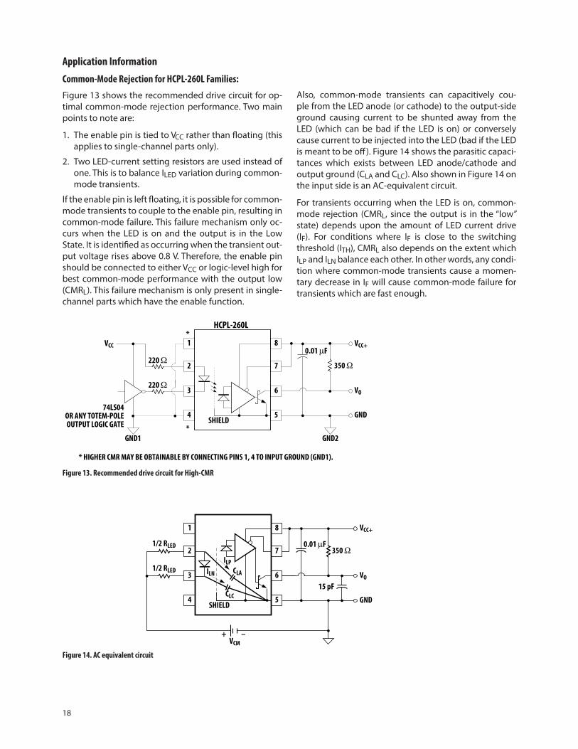
Also, common-mode transients can capacitively cou-ple from the LED anode (or cathode) to the output-side ground causing current to be shunted away from the LED (which can be bad if the LED is on) or conversely cause current to be injected into the LED (bad if the LED is meant to be off). Figure 14 shows the parasitic capaci-tances which exists between LED anode/cathode and output ground (CLA and CLC). Also shown in Figure 14 on the input side is an AC-equivalent circuit.
For transients occurring when the LED is on, common-mode rejec tion (CMRL, since the output is in the “low” state) depends upon the amount of LED current drive (IF). For conditions where IF is close to the switching threshold (ITH), CMRL also depends on the extent which ILP and ILN balance each other. In other words, any condi-tion where common-mode transients cause a momen-tary decrease in IF will cause common-mode failure for transients which are fast enough.
Application Information
Common-Mode Rejection for HCPL-260L Families:
Figure 13 shows the recom mended drive circuit for op-timal common-mode rejection performance. Two main points to note are:
1. The enable pin is tied to VCC rather than floating (this applies to single-channel parts only).
2. Two LED-current setting resistors are used instead of one. This is to balance ILED variation during common-mode transients.
If the enable pin is left floating, it is possible for common-mode transients to couple to the enable pin, resulting in common-mode failure. This failure mechanism only oc-curs when the LED is on and the output is in the Low State. It is identified as occurring when the transient out-put voltage rises above 0.8 V. Therefore, the enable pin should be connected to either VCC or logic-level high for best common-mode performance with the output low (CMRL). This failure mechanism is only present in single-channel parts which have the enable function.
0.01 µF
350 Ω
74LS04OR ANY TOTEM-POLEOUTPUT LOGIC GATE
VO
VCC+8
7
6
1
3
SHIELD5
2
4
HCPL-260L
GND
GND2
220 Ω
VCC
220 Ω
*
*
* HIGHER CMR MAY BE OBTAINABLE BY CONNECTING PINS 1, 4 TO INPUT GROUND (GND1).
GND1
350 Ω1/2 RLED
VCC+
15 pF
+VCM
8
7
6
1
3
SHIELD5
2
4
CLA VO
GND
0.01 µF
1/2 RLED
CLC
ILN
ILP
–
For product information and a complete list of distributors, please go to our website: www.avagotech.com
Avago, Avago Technologies, and the A logo are trademarks of Avago Technologies in the United States and other countries.Data subject to change. Copyright © 2005-2014 Avago Technologies. All rights reserved. Obsoletes AV01-0581EN AV02-0616EN - July 11, 2014
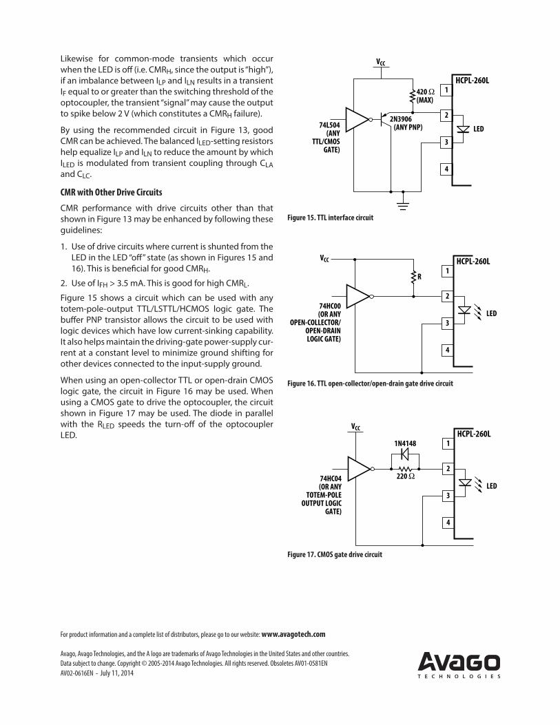
Likewise for common-mode transients which occur when the LED is off (i.e. CMRH, since the output is “high”), if an imbalance between ILP and ILN results in a transient IF equal to or greater than the switching threshold of the optocoupler, the transient “signal” may cause the output to spike below 2 V (which consti tutes a CMRH failure).
By using the recommended circuit in Figure 13, good CMR can be achieved. The balanced ILED-setting resistors help equalize ILP and ILN to reduce the amount by which ILED is modulated from transient coupling through CLA and CLC.
CMR with Other Drive Circuits
CMR performance with drive circuits other than that shown in Figure 13 may be enhanced by following these guidelines:
1. Use of drive circuits where current is shunted from the LED in the LED “off” state (as shown in Figures 15 and 16). This is beneficial for good CMRH.
2. Use of IFH > 3.5 mA. This is good for high CMRL.
Figure 15 shows a circuit which can be used with any totem-pole-output TTL/LSTTL/HCMOS logic gate. The buffer PNP transistor allows the circuit to be used with logic devices which have low current-sinking capability. It also helps maintain the driving-gate power-supply cur-rent at a constant level to minimize ground shifting for other devices connected to the input-supply ground.
When using an open-collector TTL or open-drain CMOS logic gate, the circuit in Figure 16 may be used. When using a CMOS gate to drive the optocoupler, the circuit shown in Figure 17 may be used. The diode in parallel with the RLED speeds the turn-off of the optocoupler LED.
Figure 15. TTL interface circuit
Figure 16. TTL open-collector/open-drain gate drive circuit
Figure 17. CMOS gate drive circuit
420 Ω(MAX)
1
3
2
4
2N3906 (ANY PNP)
VCC
74L504(ANY
TTL/CMOSGATE)
HCPL-260L
LED
R1
3
2
4
VCC
74HC00(OR ANY
OPEN-COLLECTOR/OPEN-DRAINLOGIC GATE)
HCPL-260L
LED
220 Ω
1
3
2
4
VCC
74HC04(OR ANY
TOTEM-POLEOUTPUT LOGIC
GATE)
HCPL-260L1N4148
LED


![AV02-0940EN DS 6N137 29Mar2010 - Farnell element14 · NO HCPL-4661 HCPL-0661 1,000 50 YES HCPL-2602[1] 3, 500 300 ... HCPL-2601/11/30/31, HCPL-4661) 8-pin DIP Package with Gull Wing](https://img.pdfslide.net/doc/110x75/5ae874c47f8b9aee078f8e91/av02-0940en-ds-6n137-29mar2010-farnell-hcpl-4661-hcpl-0661-1000-50-yes-hcpl-26021.jpg)


![Data Sheet - RS Components Internationaldocs-europe.electrocomponents.com/webdocs/0ad5/0900766b80ad52… · NO HCPL-4661 HCPL-0661 1,000 50 YES HCPL-2602[1] 3 , 500 300 ... HCPL-2601/11/30/31,](https://img.pdfslide.net/doc/110x75/5ae874c47f8b9aee078f8e9c/data-sheet-rs-components-internationaldocs-no-hcpl-4661-hcpl-0661-1000-50.jpg)