Embed Size (px)
Citation preview
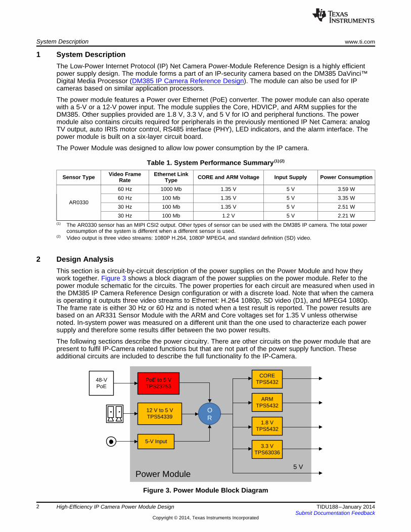
Power Module
48-VPoE
PoE to 5 VTPS23753
12 V to 5 VTPS54339
5-V Input
OR
5 V
CORE TPS5432
ARMTPS5432
1.8 VTPS5432
3.3 VTPS63036
Mark Knapp
TI DesignsHigh-Efficiency IP Camera Power Module Design
TI Designs Design FeaturesTI Designs provide the foundation that you need • Enables Class 1 PoE system power in a 1080p IPincluding methodology, testing and design files to Camera.quickly evaluate and customize and system. TI • IP Camera solution power as low as 2.2 W forDesigns help you accelerate your time to market 1080p30 with 5-V input.
• 90% efficiency on 5-V operation. 78% efficient onDesign ResourcesPoE operation.
Design FolderSAT0027 • Lower system heat generation simplifies packagedesign.TPS23753A Product Folder
TPS54339 Product Folder • Cost effective compared with many PMIC solutions.TPS5432 Product Folder Featured ApplicationsTPS63036 Product Folder • DM385 IP Camera Reference DesignTPS3839G33 Product FolderTPS3897A Product Folder
ASK Our Analog ExpertsWebBench Calculator Tools
Figure 2. Power Module Block Diagram
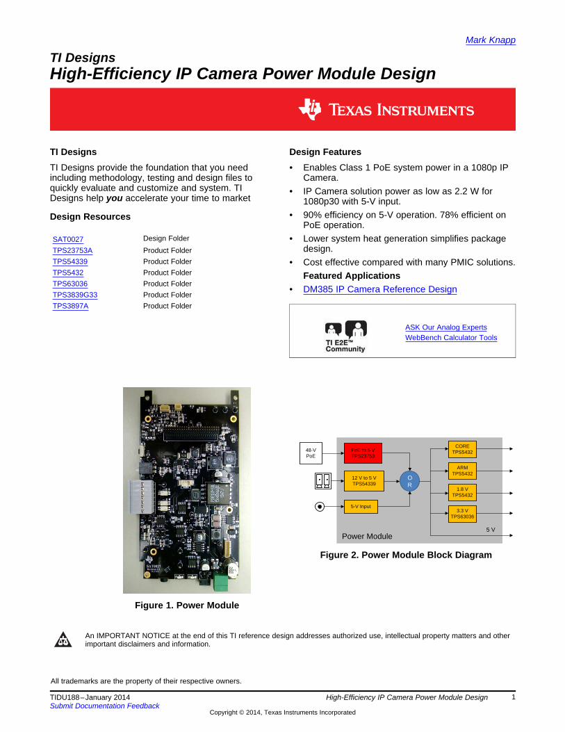
Figure 1. Power Module
An IMPORTANT NOTICE at the end of this TI reference design addresses authorized use, intellectual property matters and otherimportant disclaimers and information.
All trademarks are the property of their respective owners.
1TIDU188–January 2014 High-Efficiency IP Camera Power Module DesignSubmit Documentation Feedback
Copyright © 2014, Texas Instruments Incorporated
Power Module
48-VPoE
PoE to 5 VTPS23753
12 V to 5 VTPS54339
5-V Input
OR
5 V
CORE TPS5432
ARMTPS5432
1.8 VTPS5432
3.3 VTPS63036
System Description www.ti.com
1 System DescriptionThe Low-Power Internet Protocol (IP) Net Camera Power-Module Reference Design is a highly efficientpower supply design. The module forms a part of an IP-security camera based on the DM385 DaVinci™Digital Media Processor (DM385 IP Camera Reference Design). The module can also be used for IPcameras based on similar application processors.
The power module features a Power over Ethernet (PoE) converter. The power module can also operatewith a 5-V or a 12-V power input. The module supplies the Core, HDVICP, and ARM supplies for theDM385. Other supplies provided are 1.8 V, 3.3 V, and 5 V for IO and peripheral functions. The powermodule also contains circuits required for peripherals in the previously mentioned IP Net Camera: analogTV output, auto IRIS motor control, RS485 interface (PHY), LED indicators, and the alarm interface. Thepower module is built on a six-layer circuit board.
The Power Module was designed to allow low power consumption by the IP camera.
Table 1. System Performance Summary (1) (2)
Video Frame Ethernet LinkSensor Type CORE and ARM Voltage Input Supply Power ConsumptionRate Type60 Hz 1000 Mb 1.35 V 5 V 3.59 W60 Hz 100 Mb 1.35 V 5 V 3.35 W
AR033030 Hz 100 Mb 1.35 V 5 V 2.51 W30 Hz 100 Mb 1.2 V 5 V 2.21 W
(1) The AR0330 sensor has an MIPI CSI2 output. Other types of sensor can be used with the DM385 IP camera. The total powerconsumption of the system is different when a different sensor is used.
(2) Video output is three video streams: 1080P H.264, 1080P MPEG4, and standard definition (SD) video.
2 Design AnalysisThis section is a circuit-by-circuit description of the power supplies on the Power Module and how theywork together. Figure 3 shows a block diagram of the power supplies on the power module. Refer to thepower module schematic for the circuits. The power properties for each circuit are measured when used inthe DM385 IP Camera Reference Design configuration or with a discrete load. Note that when the camerais operating it outputs three video streams to Ethernet: H.264 1080p, SD video (D1), and MPEG4 1080p.The frame rate is either 30 Hz or 60 Hz and is noted when a test result is reported. The power results arebased on an AR331 Sensor Module with the ARM and Core voltages set for 1.35 V unless otherwisenoted. In-system power was measured on a different unit than the one used to characterize each powersupply and therefore some results differ between the two power results.
The following sections describe the power circuitry. There are other circuits on the power module that arepresent to fulfil IP-Camera related functions but that are not part of the power supply function. Theseadditional circuits are included to describe the full functionality fo the IP-Camera.
Figure 3. Power Module Block Diagram
2 High-Efficiency IP Camera Power Module Design TIDU188–January 2014Submit Documentation Feedback
Copyright © 2014, Texas Instruments Incorporated
TPS23753
TPS54339
TPS63036
TPS5432
www.ti.com Design Analysis
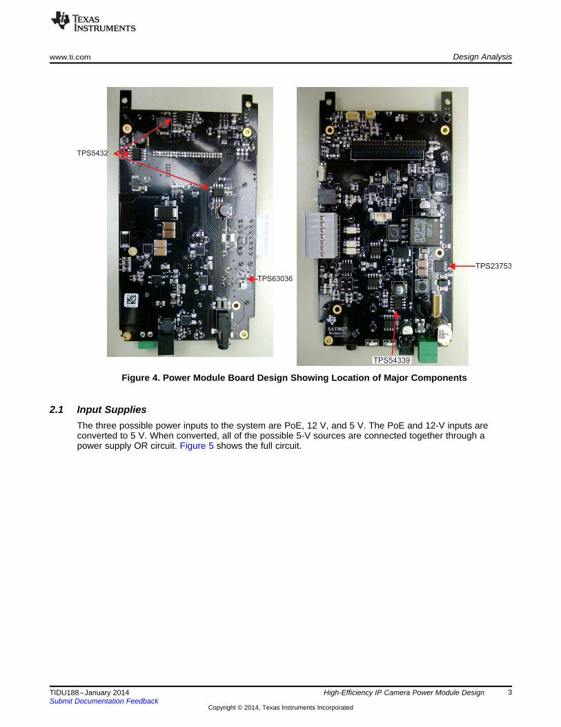
Figure 4. Power Module Board Design Showing Location of Major Components
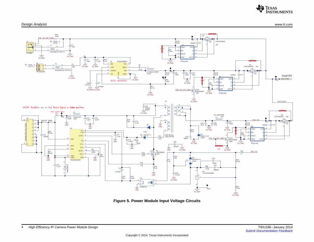
2.1 Input SuppliesThe three possible power inputs to the system are PoE, 12 V, and 5 V. The PoE and 12-V inputs areconverted to 5 V. When converted, all of the possible 5-V sources are connected together through apower supply OR circuit. Figure 5 shows the full circuit.
3TIDU188–January 2014 High-Efficiency IP Camera Power Module DesignSubmit Documentation Feedback
Copyright © 2014, Texas Instruments Incorporated
DC power in
( 5V/2A )
( 12V/1A )
DC power in
0.05
R1
DC_GND
40-57 VDC
NOTE: Rectifiers are on Sub Board Signal is taken after rectifiers
i
High Current Trace
DC_GND
DC_GND
DC_GND
0.1µF
C5
DC_GND
1000pFC12
0.1µFC16
GND
90.9R9
59.0kR7 80.6k
R8
24.9kR6
GND
22µFC13
GND
10µH
L2
744042100
2.2µFC14
2.2µFC15
GND
1
2
4
3
U5
FODM121
GND
2.00kR15
402R14
0.047µF
C21
0.1µFC17
GND
47,8
1,2
,3
5,6
,
150V
Q3FDMC86240
10.0
R12
1.0k
R13
0.33R16
GND
0.22µFC19
10µF
C20
GND
13D3 BAS16-7-F
10.0
R11
GND
1.25V
D20.1µFC1839k
R10
2200pF
C23
GND DC_GND
0.55V
D4B540C-13-F
680pFC24
DC_GND
47µFC25
47µFC26 100µF
C27
1µHL3
ELL-6RH1R0M
DC_GND DC_GND
VOUT_POE
1.0kR17
10kR18
0.47µFC28
DC_GND
DC_GND
0
R21
44.2kR22
10.0k
R20
100pF
C29
6800pF
C30
14.3kR23
DC_GND
NOTE: fsw=600kHz
VBST1
VIN2
SW3
GND4
VFB5
VREG56
EN7
SS8
PA
D9
U2 TPS54339DDA
22.1kR4
22pFC8
DC_GND
DC_GND
0.47µFC6
0.1µFC4
DC_GND
4700pF
C7
Vout=5V
RSET1
EN2
RSVD3
GND4
GATE5
C6
A7
BYP8
TPS2419D
U1
RSET1
EN2
RSVD3
GND4
GATE5
C6
A7
BYP8
TPS2419D
U3
DC_GND
154kR2
2200pF C2
2200pF C11
154kR5
10µFC1
10µF
25
C3
DC_GND
CTL1
V B2
CS3
VC4
GATE5
RTN6
VSS7
VDD18
VDD9
DEN10
CLS11
APD12
BLNK13
FRS14
U4
TPS23753APW
RSET1
EN2
RSVD3
GND4
GATE5
C6
A7
BYP8
TPS2419D
U62200pF C31
154kR24
25V4
7,81,2,3
5,6,
Q1
CSD16409Q3
25V
4
7,81,2,3
5,6,
Q2CSD16409Q3
25V
4
7,81,2,3
5,6,
Q4CSD16409Q3
0.65V
1
3
2
D5BAT54S-7-F
DC_GND
DC_GND
0R121
DNP
0
R124DNP
0
R126DNP
TP2
TP1
TP5
TP4
TP6
20.0kR123
20.0kR125
124kR3
10.0R122
TP3
20.0kR135
2200pF2000V
C22
21
D1
SM
AJ58A
ACM7060-701-2PL-TL
1
2 3
4T1
1
2
3
4
8
10
9
777
POE13P-50L
T3
POE13P-50L
TLV431ACDBZR
23
1
D6
TB-F022C00
11
22
J2
ACM4532-601-2P-T001
1
2 3
4T2
20.0R19
22µFC9
22µFC10
DC_GND
1.0kR141
PJ-052D
2
31
4J1
11
22
33
44
55
66
77
88
99
1010
J3
BM
08B
-SR
SS
-TB
(LF
)(S
N)
TP23
4.7µH
L1
VLC6045T-4R7M
0R120
DNP
0R136
DNP
0R137
DNP
DC_GND
10.0kR58
POE_12V_OFF_CONT
1
23
60V
Q152N7002KW
1
23
60V
Q162N7002KW
POE_+5V
POE_+5VDC_GND
DC_GND
POE_12V_OFF_CONT
POE_12V_OFF_CONT
4.99k
R138DNP
DNP
VOUT_POE
Design Analysis www.ti.com
Figure 5. Power Module Input Voltage Circuits
4 High-Efficiency IP Camera Power Module Design TIDU188–January 2014Submit Documentation Feedback
Copyright © 2014, Texas Instruments Incorporated
Outp
ut V
oltage
Output Current
0 0.5 1 1.5 2 2.5
3.5
4
4.5
5
5.5
3
Effic
ien
cy
Output Current
0 0.5 1 1.5 2
10
20
30
90
100
0
40
50
60
70
80
2.5
www.ti.com Design Analysis
2.1.1 5-V InputA barrel connector provides the 5-V input. The 5-V input is intended for use with an appropriately-sizedDC supply. The input path incorporates a low-pass filter to reduce EMI from being conducted into or out ofthe camera. The external 5 V then connects to a TPS2419D power-supply OR controller (U1 plus Q1).The barrel connector has a switch that disengages when the barrel is inserted. This function ensures thatthe 12-V and PoE input OR controllers are disabled. See Section 2.1.4 for additional information on thisfunction. When the camera streams 1080p at 30 Hz the input power is 3.48 W with a 5-V input supplywhen using 1.35 V for the ARM and Core supplies and an AR331 image sensor is used.
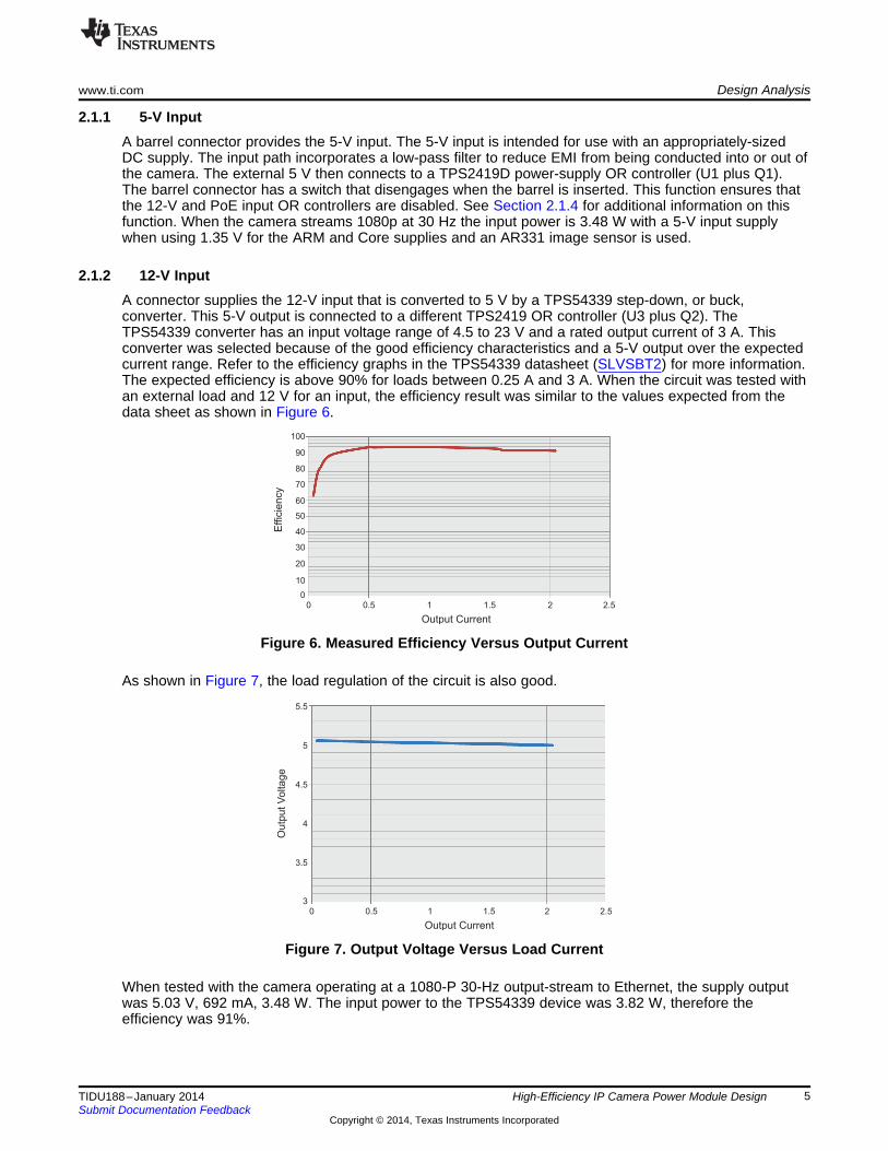
2.1.2 12-V InputA connector supplies the 12-V input that is converted to 5 V by a TPS54339 step-down, or buck,converter. This 5-V output is connected to a different TPS2419 OR controller (U3 plus Q2). TheTPS54339 converter has an input voltage range of 4.5 to 23 V and a rated output current of 3 A. Thisconverter was selected because of the good efficiency characteristics and a 5-V output over the expectedcurrent range. Refer to the efficiency graphs in the TPS54339 datasheet (SLVSBT2) for more information.The expected efficiency is above 90% for loads between 0.25 A and 3 A. When the circuit was tested withan external load and 12 V for an input, the efficiency result was similar to the values expected from thedata sheet as shown in Figure 6.
Figure 6. Measured Efficiency Versus Output Current
As shown in Figure 7, the load regulation of the circuit is also good.
Figure 7. Output Voltage Versus Load Current
When tested with the camera operating at a 1080-P 30-Hz output-stream to Ethernet, the supply outputwas 5.03 V, 692 mA, 3.48 W. The input power to the TPS54339 device was 3.82 W, therefore theefficiency was 91%.
5TIDU188–January 2014 High-Efficiency IP Camera Power Module DesignSubmit Documentation Feedback
Copyright © 2014, Texas Instruments Incorporated
DIFFERENTIAL PAIR100 OHM DIFFERENTIALIMPEDANCESHORT AND STRAIGHT ASPOSSIBLE,MINIMUM NUMBER OF VIAS
RJ45_D1+
RJ45_D1-
RJ45_D2+
D2_REC1
D2_REC2
RJ45_D2-
RJ45_D3+
RJ45_D3-
D7_REC2
RJ45_D4+
RJ45_D4-
D7_REC1
1000 BASE350 mA
1000 BASE350 mA
1CT : 1CT
1CT : 1CT
1CT : 1CT
1CT : 1CT
TCT1
TD1+
TD1-
TCT2
TCT3
TCT4
MCT1
MX1+
MX1-
TD2+
TD2-
TD3-
TD4-
TD3+
TD4+
( Chip Side )( Media Side )
MCT2
MCT3
MCT4
MX2+
MX3+
MX4+
MX2-
MX3-
MX4-
1
2
3
4
5
6
7
8
9
10
11
1213
14
15
16
17
18
19
20
21
22
23
24
T1 H5084NL
TRD0_P
TRD2_P
TRD3_P
TRD0_N
TRD2_N
TRD3_N
TRD1_PTRD1_N
D1+1
GND2
D2+3
D2-4
VCC5
D1-6
U10
TPD4S009DCK
D1+1
GND2
D2+3
D2-4
VCC5
D1-6
U12
TPD4S009DCK
0.1µF
C83
0.1µF
C89
0.1µF
C82
0.1µF
C85
0.1µF
C93
0.1µF
C88
RJ45_D1-
RJ45_D4-
RJ45_D3-
RJ45_D1+
RJ45_D2+
RJ45_D3+
RJ45_D2-
RJ45_D4+
LED_ACT
VCC3.3VDLED_100_10
LED_LINK
Ethernet Active : High => turn on
LED_LINK(green LED)
100M : Low => turn on
10M : High => turn off
LED_100/10(yellow LED)
D2_REC1
D2_REC2
0.01µFC92
0.01µFC94
0.01µFC95
0.01µFC96
1000pFC91
220R93
220R96
75.0R98
75.0R100
75.0R101
75.0R102
1000(100)
BI_D4-(NC)8
BI_D4+(NC)7
BI_D2-(RX_D2-)6
BI_D3-(NC)5
BI_D3+(NC)4
BI_D2+(RX_D2+)3
BI_D1-(TX_D1-)2
BI_D1+(TX_D1+)1
SP
19
SP
21
0
G_LED1-11
G_LED1+12
Y_LED2+13
Y_LED2-14
J66116075-4
0.1µFC126
0.1µFC127
D7_REC1
D7_REC2
( 48V )
D2_REC1D2_REC2
D7_REC2 D7_REC1
1000pFC111
MMZ2012R150A
FB1
MMZ2012R150A
FB2
+
-
3
1
4
2
D7
+
-
3
1
4
2
D2
11
22
33
44
55
66
77
88
99
1010
J9
BM
08
B-S
RS
S-T
B(L
F)(
SN
)
Design Analysis www.ti.com
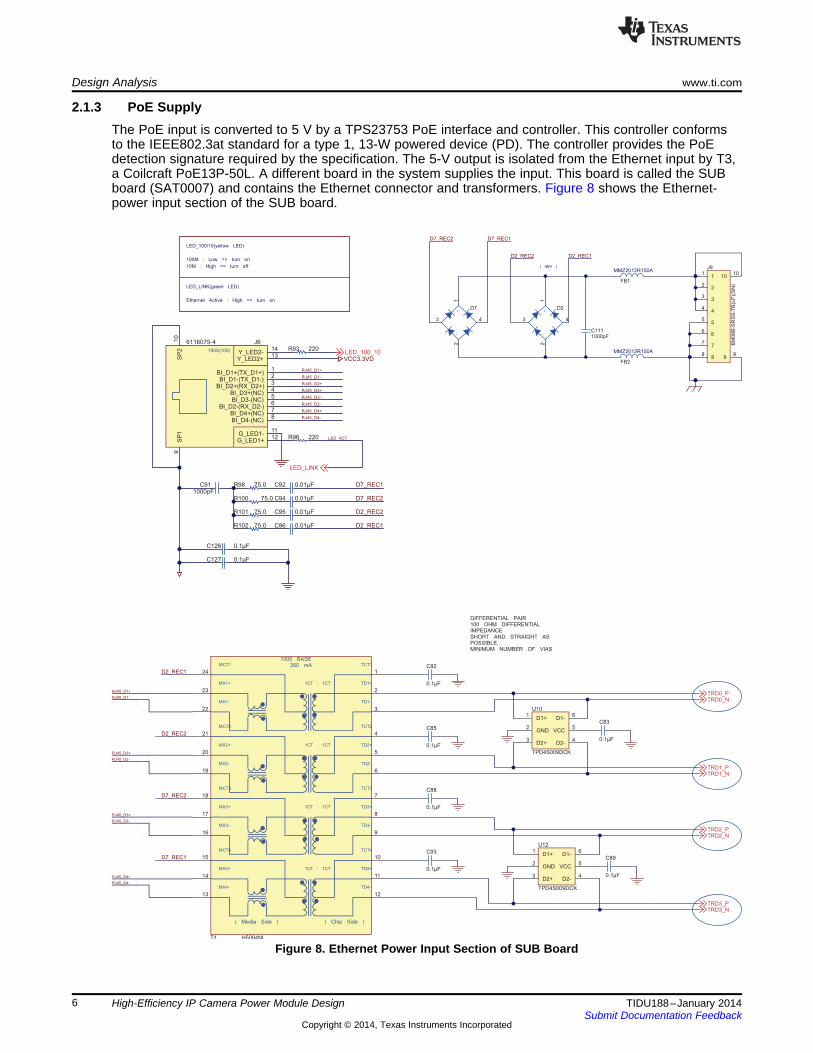
2.1.3 PoE SupplyThe PoE input is converted to 5 V by a TPS23753 PoE interface and controller. This controller conformsto the IEEE802.3at standard for a type 1, 13-W powered device (PD). The controller provides the PoEdetection signature required by the specification. The 5-V output is isolated from the Ethernet input by T3,a Coilcraft PoE13P-50L. A different board in the system supplies the input. This board is called the SUBboard (SAT0007) and contains the Ethernet connector and transformers. Figure 8 shows the Ethernet-power input section of the SUB board.
Figure 8. Ethernet Power Input Section of SUB Board
6 High-Efficiency IP Camera Power Module Design TIDU188–January 2014Submit Documentation Feedback
Copyright © 2014, Texas Instruments Incorporated
Outp
ut V
oltage
Output Current
0 0.5 1 1.5 2.5 3
3.5
4
4.5
5
5.5
32
6
Effic
iency
Output Current
0 0.5 1 1.5 2 3
10
20
30
90
100
0
40
50
60
70
80
2.5
www.ti.com Design Analysis
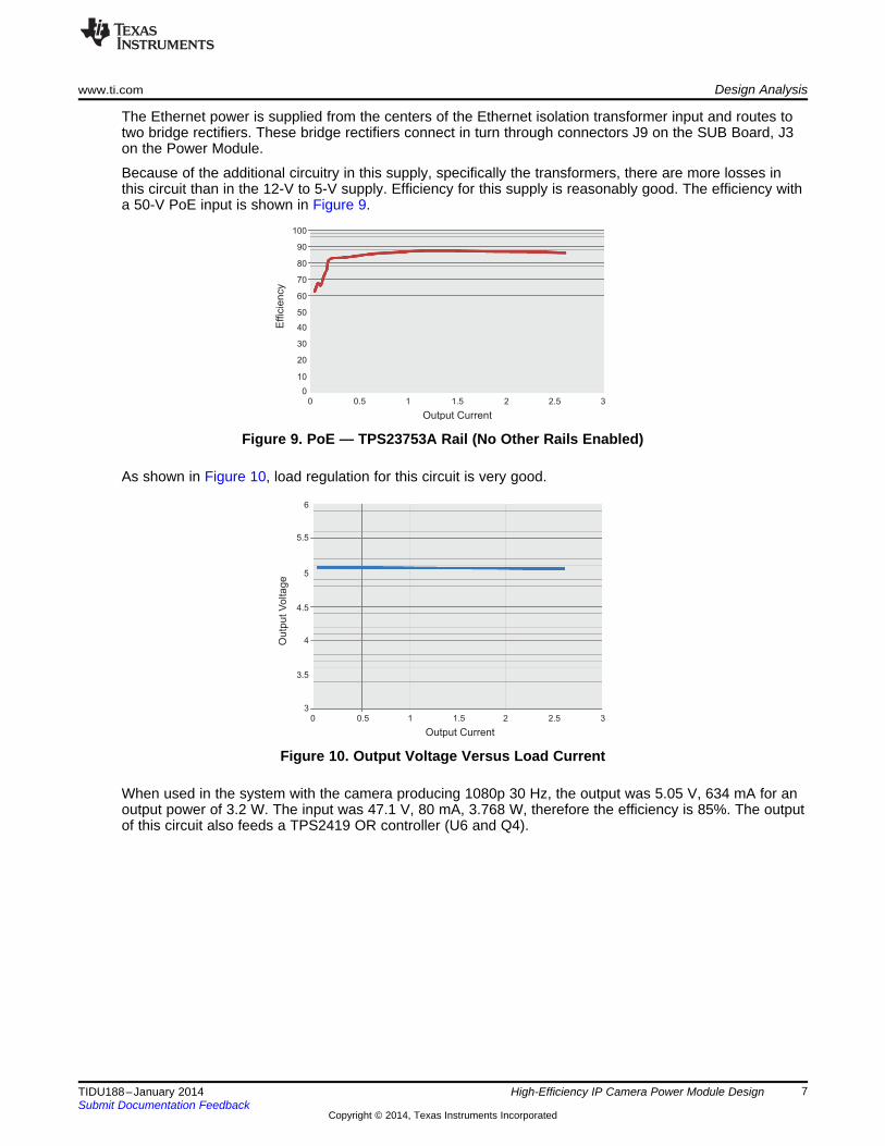
The Ethernet power is supplied from the centers of the Ethernet isolation transformer input and routes totwo bridge rectifiers. These bridge rectifiers connect in turn through connectors J9 on the SUB Board, J3on the Power Module.
Because of the additional circuitry in this supply, specifically the transformers, there are more losses inthis circuit than in the 12-V to 5-V supply. Efficiency for this supply is reasonably good. The efficiency witha 50-V PoE input is shown in Figure 9.
Figure 9. PoE — TPS23753A Rail (No Other Rails Enabled)
As shown in Figure 10, load regulation for this circuit is very good.
Figure 10. Output Voltage Versus Load Current
When used in the system with the camera producing 1080p 30 Hz, the output was 5.05 V, 634 mA for anoutput power of 3.2 W. The input was 47.1 V, 80 mA, 3.768 W, therefore the efficiency is 85%. The outputof this circuit also feeds a TPS2419 OR controller (U6 and Q4).
7TIDU188–January 2014 High-Efficiency IP Camera Power Module DesignSubmit Documentation Feedback
Copyright © 2014, Texas Instruments Incorporated
PWR_1V8
22µFC44
DC_GND
0.1µF
C43
DC_GND
8.25k
1%
R42
PWR_1V8 Rail
Output Set to 1.8V
22µFC45
0.1µFC46
1000pFC47
10.0k1%
R41
49.9
1%
R40
TP14
TP13
MAIN_VDD
EN_1v8
DC_GND
DC_GND
DC_GND
0.1µF
C38
1.00kR39
0.1µFC41
820pFC40
10µF
C39
0.01µFC42
0
R132
DC_GND
BOOT1
VIN2
PH3
GND4
VSENSE5
COMP6
EN7
SS8
T-PAD9
U11
TPS5432DDA
6.8µH
L6
VLC6045T-6R8M
Design Analysis www.ti.com
2.1.4 OR ControllersThe TPS2419 OR controllers are the interface between the various 5-V supplies and the remainder of thesystem. The outputs of the PoE-to-5-V and 12-V-to-5-V converters are set at slightly different voltages toensure that the 12-V OR controller is off when PoE is present. The 5-V input ranges from 4.75 to 5.25 V.Because of this voltage range, the OR controller can source current from either the 5-V input or one of theother inputs depending on whether the other inputs are present and whether the voltage at the 5-V input isbelow the output of the PoE or 12-V-to-5-V converter.
When only one input voltage is available, there can be some leakage through the OR controller circuitsback into the other inputs. Because of this leakage, the 5-V input connector controls additional circuitry. Ifa 5-V input barrel-connector is present, the signal PoE_12V_OFF_CONT is pulled high. Pulling the signalhigh turns on Q15 and Q16 which then disable the OR controllers U3 and U6. To ensure that only oneinput supplies the camera at a time and that there is a preference order for the inputs, additional circuitrycould be added. The output of the OR controller circuitry is a single 5-V power supply VOUT_POE.
2.2 Electronics Supply RailsAfter the OR controller circuit, there is a common 5-V supply for the rest of the system. This signalsupplies all other power conversion in the system, including the DDR supply on the processor board(SAT0008) and the IRIS controller on the Power Module. The following sections describe the individualpower supply circuits in the order that the supplies are enabled. All performance tests listed inSection 2.2.1 through Section 2.2.4 were performed with a 5-V input.
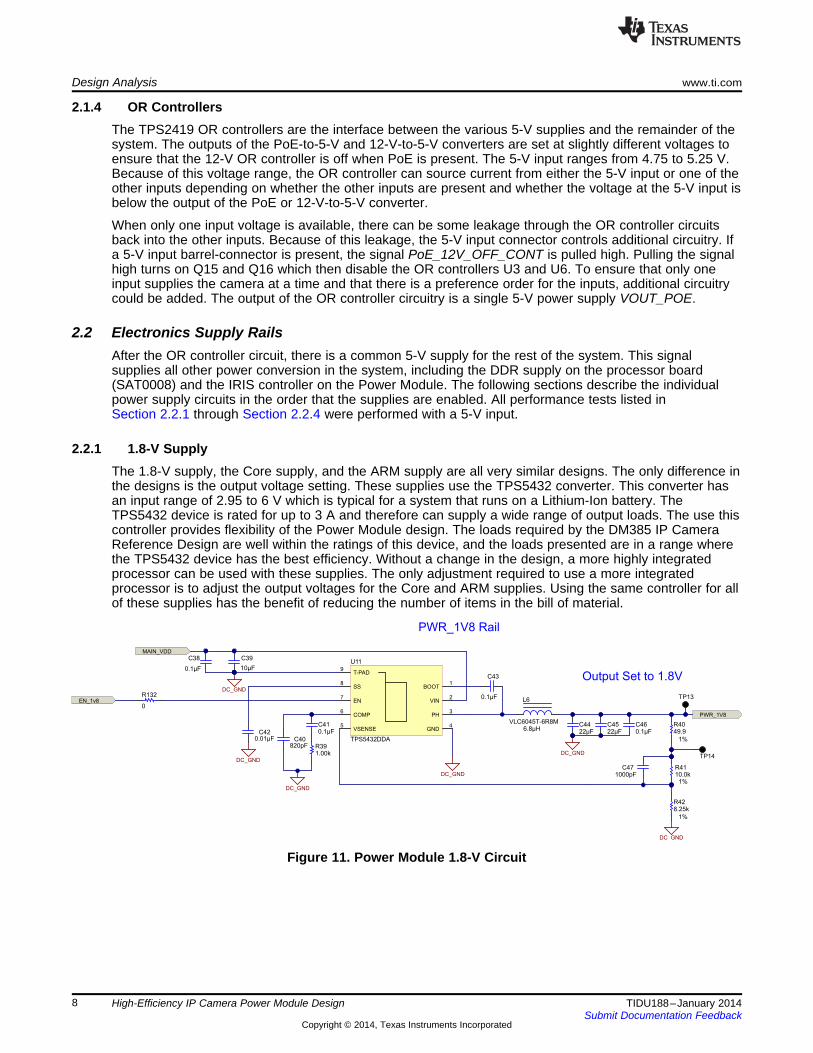
2.2.1 1.8-V SupplyThe 1.8-V supply, the Core supply, and the ARM supply are all very similar designs. The only difference inthe designs is the output voltage setting. These supplies use the TPS5432 converter. This converter hasan input range of 2.95 to 6 V which is typical for a system that runs on a Lithium-Ion battery. TheTPS5432 device is rated for up to 3 A and therefore can supply a wide range of output loads. The use thiscontroller provides flexibility of the Power Module design. The loads required by the DM385 IP CameraReference Design are well within the ratings of this device, and the loads presented are in a range wherethe TPS5432 device has the best efficiency. Without a change in the design, a more highly integratedprocessor can be used with these supplies. The only adjustment required to use a more integratedprocessor is to adjust the output voltages for the Core and ARM supplies. Using the same controller for allof these supplies has the benefit of reducing the number of items in the bill of material.
Figure 11. Power Module 1.8-V Circuit
8 High-Efficiency IP Camera Power Module Design TIDU188–January 2014Submit Documentation Feedback
Copyright © 2014, Texas Instruments Incorporated
Outp
ut V
oltage
Output Current
0 0.4 0.6 1 1.2 1.8
1.55
1.6
1.65
1.95
2
1.5
1.7
1.75
1.8
1.85
1.9
1.60.8 1.40.2
Effic
iency
Output Current
0 0.4 0.6 1 1.2 1.8
10
20
30
90
100
0
40
50
60
70
80
1.60.8 1.40.2
100
95
90
85
80
75
70
65
60
55
50
Eff
icie
nc
y (
%)
0 500 1000 1500 2000 2500 3000
Load Current (mA)
V = 5 V, V = 1.2 VI O
V VI O= 3.3 V, = 1.2 V
V VI O= 5 V, = 1.8 V
V VI O= 3.3 V, = 1.8 V
V VI O= 5 V, = 3.3 V
www.ti.com Design Analysis
The TPS5432 device is very efficient in the in the range of output voltages and currents used in theDM385 IP Camera. For the loads in question (below 1 A), the efficiency is at or above 90% as shown inFigure 12. For more information on the TPS5432 device, see the data sheet SLVSB89.
Figure 12. TPS5432 Efficiency Curve
When used in the power module, the 1.8-V supply results were similar to the TPS5432 efficiency curve asshown in Figure 13
Figure 13. 1.8-V TPS5432 Rail (No Other Rails Enabled)
As show in Figure 14, load regulation for this circuit was also very good.
Figure 14. Output Voltage Versus Load Current
9TIDU188–January 2014 High-Efficiency IP Camera Power Module DesignSubmit Documentation Feedback
Copyright © 2014, Texas Instruments Incorporated
Design Analysis www.ti.com
At system startup, the rise time for the 1.8-V supply is about 3.9 ms (see Figure 15).
Figure 15. Rise Time — 1.8-V Supply
For a camera streaming 1080p 30-Hz video, the 1.8-V load is only 103 mA which is low for this supply.Output power is 185 mW, while the input power is 206 mW. Therefore the efficiency is 90%.
10 High-Efficiency IP Camera Power Module Design TIDU188–January 2014Submit Documentation Feedback
Copyright © 2014, Texas Instruments Incorporated
Output Current - mA
Eff
icie
nc
y-
%
0
10
20
30
40
50
60
70
80
90
100
0.1 1 10 100 1000
V = 2.4 V, V = 3.3 VI O
V = 3.6 V, V = 3.3 VI O
Input Voltage - V
Eff
icie
ncy -
%
0
10
20
30
40
50
60
70
80
90
100
1.8 2.2 2.6 3 3.4 3.8 4.2 4.6 5 5.4 5.8
V = 3.3 VO
I = 100 mAO
I = 10 mAO
I = 500 mAO
Power Save Enabled
MAIN_VDD
EN_3V3
DC_GND
DC_GND
INT_3V3 Rail
0.1µFC48
Output Set to 3.3V
10µFC49
10.0kR44
10.0R43
DC_GND
0
R131
PWR_3V3
287k1%
R45
DC_GND DC_GND DC_GND
51.1k 1%R46
DC_GND
10µFC51
10µFC52
10µFC53
10pFC50
TP11
TP12
49.90.5%
R140
1.5µH
L7
LPS3015-152MLB
TPS63036YFGR
VIN1A
EN2A
L11B
PS/SYNC2B
L21C
GND2C
VOUT1D
FB2D
U12
www.ti.com Design Analysis
2.2.2 3.3-V SupplyThe 3.3-V supply uses a TPS63036 buck-boost controller. A buck-boost controller is used to allow themain power supply rails for the camera processing to run from a Lithium Ion battery, if desired. With thebattery, the input voltage can drop as low as 3 V. The buck-boost topology maintains the 3.3-V outputvoltage when the battery voltage drops to 3.3 V or below. In the standard application the TPS63036 staysin buck mode because a battery is not used. Figure 17 and Figure 18 show the TPS63036 efficiencycurves for a 3.3-V output voltage with Power Save Mode enabled.
Figure 16. Power Module 3.3-V Circuit
Figure 17. Efficiency vs Output Current Figure 18. Efficiency vs Input Voltage
In-circuit performance results were good. As shown in Figure 19, efficiency is above 90% from about 125mA to 600 mA.
11TIDU188–January 2014 High-Efficiency IP Camera Power Module DesignSubmit Documentation Feedback
Copyright © 2014, Texas Instruments Incorporated
Ou
tpu
t V
olta
ge
Output Current
0 0.4 0.6 1 1.2
3.05
3.1
3.35
3.4
3
3.15
3.2
3.25
3.3
0.80.2
Effic
ien
cy
Output Current
0 0.4 0.6 1 1.2
10
20
30
90
100
0
40
50
60
70
80
0.80.2
Design Analysis www.ti.com
Figure 19. 3.3-V Supply — TPS63036 Rail (No Other Rails Enabled)
As shown in Figure 20, output voltage regulation was very good.
Figure 20. Output Voltage Versus Load Current
Note that the input voltage for the 3.3-V circuit test was 5 V.
At startup, the supply output rise time is very fast at approximately 760 ms as shown by the yellow trace inFigure 21.
12 High-Efficiency IP Camera Power Module Design TIDU188–January 2014Submit Documentation Feedback
Copyright © 2014, Texas Instruments Incorporated
www.ti.com Design Analysis
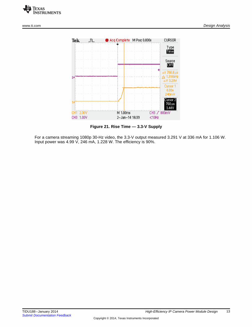
Figure 21. Rise Time — 3.3-V Supply
For a camera streaming 1080p 30-Hz video, the 3.3-V output measured 3.291 V at 336 mA for 1.106 W.Input power was 4.99 V, 246 mA, 1.228 W. The efficiency is 90%.
13TIDU188–January 2014 High-Efficiency IP Camera Power Module DesignSubmit Documentation Feedback
Copyright © 2014, Texas Instruments Incorporated
CORE_HD_VDD
DC_GND
DC_GND
0.1µF
C59
49.9 1%R48
10.0k 1%R49
INT_CORE_HD Rail
Output Voltage Rail1.1V R50=28k1.2V R50=21k1.35V R50=15k
22µFC60
22µFC61
0.1µFC62
Output Set to 1.35V
1000pFC63
TP8
TP7
BOOT1
VIN2
PH3
GND4
VSENSE5
COMP6
EN7
SS8
T-PAD9
U13
TPS5432DDA
MAIN_VDD
DC_GND
DC_GND
DC_GND
EN_CORE_HD
0.01µFC58
0.1µFC54
750R47
0.1µFC57
1000pF
C56
10µFC55
0
R129
DC_GND
CORE_HD_VDD
15.0k
R50
6.8µH
L8
VLC6045T-6R8M
INT_ARM
DC_GND
49.9 0.5%
R52
DC_GND
0.1µF
C69
INT_ARM_VDD Rail
Output Voltage Rail1.1V R54=28k1.2V R54=21k1.35V R54=15k
Output Set to 1.35V
1000pFC73
22µFC71
0.1µFC72
10.0k 1%R53
22µFC70
TP10
TP9
MAIN_VDD
EN_ARM
DC_GND
DC_GND
DC_GND
0.1µFC64
750R51
0.1µFC67
1000pF
C66
0.01µF
C68
10µFC65
0
R130
DC_GND
BOOT1
VIN2
PH3
GND4
VSENSE5
COMP6
EN7
SS8
T-PAD9
U14
TPS5432DDA
15.0kR54
6.8µH
L9
VLC6045T-6R8M
Design Analysis www.ti.com
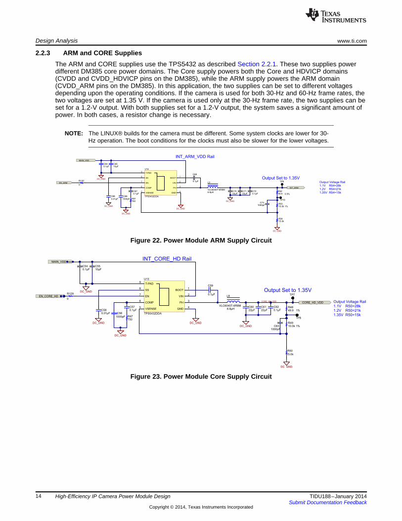
2.2.3 ARM and CORE SuppliesThe ARM and CORE supplies use the TPS5432 as described Section 2.2.1. These two supplies powerdifferent DM385 core power domains. The Core supply powers both the Core and HDVICP domains(CVDD and CVDD_HDVICP pins on the DM385), while the ARM supply powers the ARM domain(CVDD_ARM pins on the DM385). In this application, the two supplies can be set to different voltagesdepending upon the operating conditions. If the camera is used for both 30-Hz and 60-Hz frame rates, thetwo voltages are set at 1.35 V. If the camera is used only at the 30-Hz frame rate, the two supplies can beset for a 1.2-V output. With both supplies set for a 1.2-V output, the system saves a significant amount ofpower. In both cases, a resistor change is necessary.
NOTE: The LINUX® builds for the camera must be different. Some system clocks are lower for 30-Hz operation. The boot conditions for the clocks must also be slower for the lower voltages.
Figure 22. Power Module ARM Supply Circuit
Figure 23. Power Module Core Supply Circuit
14 High-Efficiency IP Camera Power Module Design TIDU188–January 2014Submit Documentation Feedback
Copyright © 2014, Texas Instruments Incorporated
Outp
ut V
oltage
Output Current
0 0.5 1 1.5 2 2.5
1.05
1.1
1.15
1.45
1.5
1
1.2
1.25
1.3
1.35
1.4
Outp
ut V
oltage
Output Current
0 1 1.5
1.05
1.1
1
1.15
1.2
0.5
Effic
iency
Output Current
0 0.5 1 1.5 2
10
20
30
90
100
0
40
50
60
70
80
2.5
Effic
iency
Output Current
0 0.5 1 1.5 2
10
20
30
90
100
0
40
50
60
70
80
www.ti.com Design Analysis
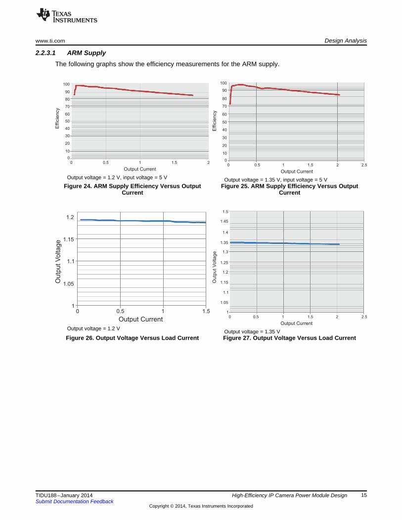
2.2.3.1 ARM SupplyThe following graphs show the efficiency measurements for the ARM supply.
Output voltage = 1.2 V, input voltage = 5 V Output voltage = 1.35 V, input voltage = 5 VFigure 24. ARM Supply Efficiency Versus Output Figure 25. ARM Supply Efficiency Versus Output
Current Current
Output voltage = 1.2 V Output voltage = 1.35 VFigure 26. Output Voltage Versus Load Current Figure 27. Output Voltage Versus Load Current
15TIDU188–January 2014 High-Efficiency IP Camera Power Module DesignSubmit Documentation Feedback
Copyright © 2014, Texas Instruments Incorporated
Outp
ut V
oltage
Output Current
0 0.5 1 1.5 2 2.5
1.05
1.1
1.15
1.45
1.5
1
1.2
1.25
1.3
1.35
1.4
Outp
ut V
oltage
Output Current
0 0.5 1 1.5 2
1.05
1.1
1.15
1
1.2
1.25
1.3
Effic
iency
Output Current
0 0.5 1 1.5 2
10
20
30
90
100
0
40
50
60
70
80
Effic
iency
Output Current
0 0.5 1 1.5 2.5
10
20
30
90
100
0
40
50
60
70
80
2
Design Analysis www.ti.com
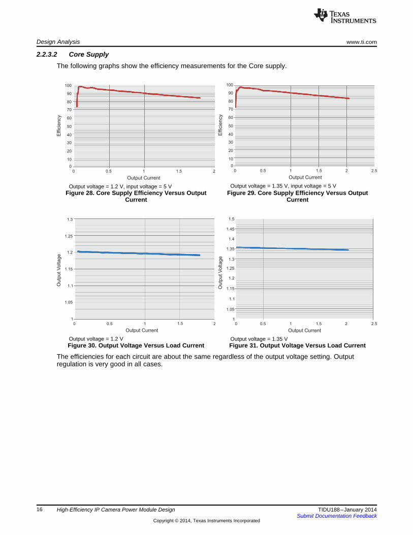
2.2.3.2 Core SupplyThe following graphs show the efficiency measurements for the Core supply.
Output voltage = 1.35 V, input voltage = 5 VOutput voltage = 1.2 V, input voltage = 5 VFigure 28. Core Supply Efficiency Versus Output Figure 29. Core Supply Efficiency Versus Output
Current Current
Output voltage = 1.2 V Output voltage = 1.35 VFigure 30. Output Voltage Versus Load Current Figure 31. Output Voltage Versus Load Current
The efficiencies for each circuit are about the same regardless of the output voltage setting. Outputregulation is very good in all cases.
16 High-Efficiency IP Camera Power Module Design TIDU188–January 2014Submit Documentation Feedback
Copyright © 2014, Texas Instruments Incorporated
www.ti.com Design Analysis
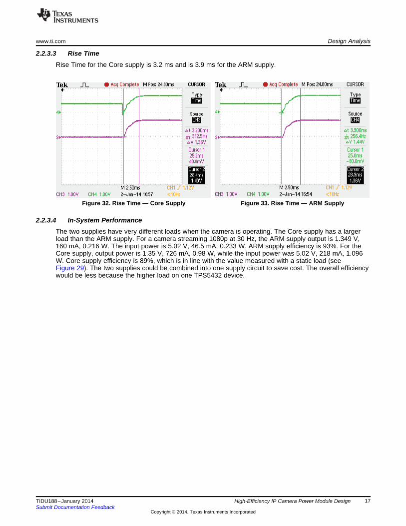
2.2.3.3 Rise TimeRise Time for the Core supply is 3.2 ms and is 3.9 ms for the ARM supply.
Figure 32. Rise Time — Core Supply Figure 33. Rise Time — ARM Supply
2.2.3.4 In-System PerformanceThe two supplies have very different loads when the camera is operating. The Core supply has a largerload than the ARM supply. For a camera streaming 1080p at 30 Hz, the ARM supply output is 1.349 V,160 mA, 0.216 W. The input power is 5.02 V, 46.5 mA, 0.233 W. ARM supply efficiency is 93%. For theCore supply, output power is 1.35 V, 726 mA, 0.98 W, while the input power was 5.02 V, 218 mA, 1.096W. Core supply efficiency is 89%, which is in line with the value measured with a static load (seeFigure 29). The two supplies could be combined into one supply circuit to save cost. The overall efficiencywould be less because the higher load on one TPS5432 device.
17TIDU188–January 2014 High-Efficiency IP Camera Power Module DesignSubmit Documentation Feedback
Copyright © 2014, Texas Instruments Incorporated
DDR3_VTT
VDDQ_1V5
VREF
EN_DDR3
DO NOT INSTALL R198 W HEN USING DDR3L
54.9
kR
198
15kR197
10kR191
49.9R132
22µH
L13
MSS5131-223MLB
10µFC75
0.1µFC76
0.1µF
C78
22µFC374
0.22µFC370
10µFC85
0.1µFC80
680pFC69
0.1µFC70
1.07kR183
1000pF
C79
TPS_INT1
DDR3_VDD_PG
IO_1.8V
IO_1.8V
BOOT1
PH3
VSENSE5
GND4
SS8
COMP6
EN7
VIN2
TP
AD
9
U19TPS5432DDAR
TPS51206DSQR
VDDQSNS1
VLDOIN2
VTT3
PGND4
VTTSNS5
VTTREF6
S37
GND8
S59
VDD10
TP
AD
11
U20
PWR_5V
TPS3808G12DBV
RESET1
GND2
MR3
CT4
SENSE5
VDD6
U21
47k
R212
IO_3.3V
2.21kR213
Design Analysis www.ti.com
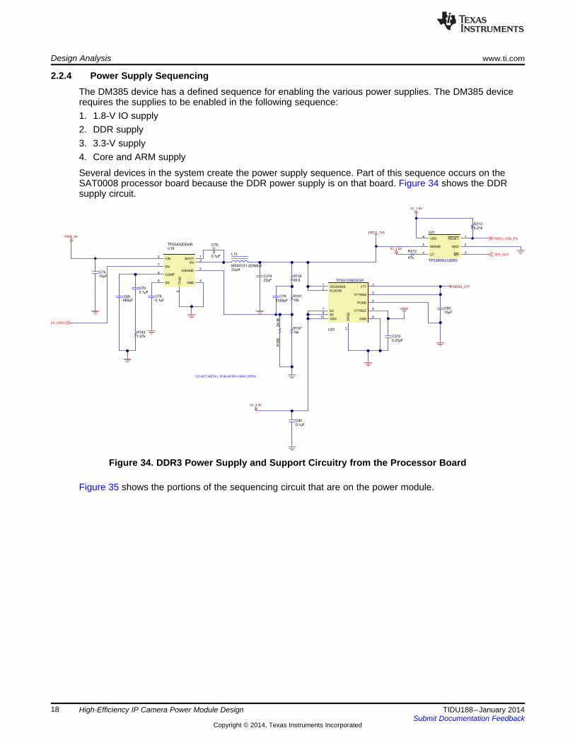
2.2.4 Power Supply SequencingThe DM385 device has a defined sequence for enabling the various power supplies. The DM385 devicerequires the supplies to be enabled in the following sequence:1. 1.8-V IO supply2. DDR supply3. 3.3-V supply4. Core and ARM supply
Several devices in the system create the power supply sequence. Part of this sequence occurs on theSAT0008 processor board because the DDR power supply is on that board. Figure 34 shows the DDRsupply circuit.
Figure 34. DDR3 Power Supply and Support Circuitry from the Processor Board
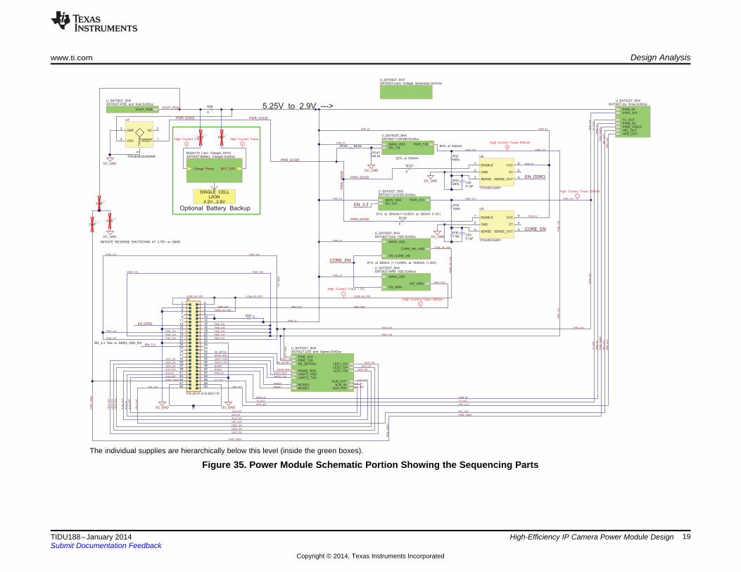
Figure 35 shows the portions of the sequencing circuit that are on the power module.
18 High-Efficiency IP Camera Power Module Design TIDU188–January 2014Submit Documentation Feedback
Copyright © 2014, Texas Instruments Incorporated
Optional Battery Backup
SINGLE CELLLiION
4.2V...2.8V
5.25V to 2.9V --->
Charge Power BAT_VDD
BQ24170 LiIon Charger_SH10SAT0027-Battery Charger.SchDoc
TV_OUT
DC_GND DC_GND
0R29
DNP
0R28
DNP
DC_GND
0R30
DNP
0R36
90% at 450mA
92% at 540mA
0
R26
0R27
DNP
91% at 300mA(1.1V)/92% at 300mA (1.2V)
91% at 520mA (1.1V)/90% at 1400mA (1.35V)
i
High Current Trace
i
High Current Trace 500mA
i
High Current Trace 500mA
i
High Current Trace 1.2A
i
High Current Trace 300mA
i
High Current Trace
EN_DDR3
EN_3.3
EN_3.3
INITIATE REVERSE SHUTDOWN AT 2.79V on MAIN
DC_GND
0R25
DNP
PWR_1V8
PWR_3V3
PWR_3V3 PWR_1V8
PWR_1V8
PWR_1V8
PWR_1V8
LED1_ON
LED1_ON
LED2_ON
LED3_ON
LED2_ON
LED3_ON
ALM_OUT
ALM_IN
ALM_RST
ALM_OUT
ALM_IN
ALM_RST
UART2_RXD
UART2_TXD
RS485_RDE
RE_SETING
MODE0
MODE1
PWM_DC
HPR_OUTHPL_OUT
PWR_1V8
PWR_3V3
DC_GND287kR33
665kR32
PWR_5V
PWR_5V
PWR_5V
PWR_5V
PWR_5V
PWR_5V
PWR_5V
PWR_5V
118kR35
DC_GND
604kR34
PWR_5V
CORE_EN
PWR_GOOD
PWR_GOOD
PW
M_V
IDE
O
PWM_VIDEO
PWM_VIDEO
PWM_VIDEO
PW
M_V
IDE
O
PW
M_V
IDE
O
HP
L_O
UT
HP
L_O
UT
HPL_OUT
HPL_OUT
HP
L_O
UT
HP
R_O
UT
HP
R_
OU
T
HPR_OUT
PW
M_D
CP
WM
_D
C
PWM_DC PWM_DC
TV
_O
UT
TV
_O
UT
TV_OUTTV_OUT
PW
R_3V
3
PWR_3V3PWR_3V3
PW
R_3V
3
PWR_3V3PWR_3V3
PWR_3V3PWR_3V3
PWR_1V8PWR_1V8
PWR_3V3
PWR_3V3
PW
R_1V
8
PWR_1V8
PW
M_V
IDE
O
LED1_ON
LE
D1_O
N
LED2_ON
LE
D2_O
N
LED3_ON
LE
D3_O
N
ALM_OUT
ALM
_O
UT
ALM_IN
ALM
_IN
ALM_RST
ALM
_R
ST
PW
R_1V
8
PWR_1V8
CO
RE
_H
D_V
DD
CORE_HD_VDDCORE_HD_VDDCORE_HD_VDD
CORE_HD_VDD
CORE_HD_VDD
ARM_VDD
ARM_VDDARM_VDD ARM_VDD
PW
R_3V
3
PWR_1V8
PW
R_3V
3
PWR_GOOD
PWR_GOOD
PWR_GOOD
PW
R_G
OO
D
RE_SETING
RS485_RDE
UART2_RXD
UART2_TXD
MODE0
MODE1
HPR_OUT
0.1µFC32
0.1µFC33
0
R127
0
R128
EN_3.3 Ties to DDR3_VDD_PG
RESET1
NC2
GND3
VDD4
T-P
ad
5
U7
TPS3839G33DQNR
ENABLE1
GND2
SENSE3
SENSE_OUT4
CT5
VCC6
U8
TPS3897ADRY
EN_DDR3
CORE_EN
ENABLE1
GND2
SENSE3
SENSE_OUT4
CT5
VCC6
U9
TPS3897ADRY
VOUT_POE
U_SAT0027_SH2SAT0027-POE and Wall.SchDoc
PWR_1V8MAIN_VDDEN_1v8
U_SAT0027_SH6SAT0027-1v8VDD.SchDoc
MAIN_VDDEN_3V3
PWR_3V3
U_SAT0027_SH5SAT0027-3v3VDD.SchDoc
CORE_HD_VDD
MAIN_VDD
EN_CORE_HD
U_SAT0027_SH3SAT0027-Core VDD.SchDoc
INT_ARM
MAIN_VDD
EN_ARM
U_SAT0027_SH4SAT0027-ARM VDD.SchDoc
PWR_5VPWR_3V3
TV_OUT
HPL_OUTHPR_OUT
PWM_VIDEOPWM_DC
U_SAT0027_SH9SAT0027-Iris Drive.SchDoc
PWR_3V3PWR_1V8
MODE1MODE0
RE_SETING
UART2_RXD
ALM_OUTALM_IN
ALM_RST
RS485_RDE
UART2_TXD
LED2_ONLED3_ON
LED1_ON
U_SAT0027_SH8SAT0027-LED and Alarms.SchDoc
FW-25-01-G-D-630-115
1 23 45 67 89 10
11 1213 1415 1617 1819 2021 2223 2425 2627 2829 3031 3233 3435 3637 3839 4041 4243 4445 4647 4849 50
J4
DC_GND
66.5kR142
46.4kR143
VOUT_POE
U_SAT0027 SH7SAT0027-Lens Voltage Generation.SchDoc
www.ti.com Design Analysis
The individual supplies are hierarchically below this level (inside the green boxes).
Figure 35. Power Module Schematic Portion Showing the Sequencing Parts
19TIDU188–January 2014 High-Efficiency IP Camera Power Module DesignSubmit Documentation Feedback
Copyright © 2014, Texas Instruments Incorporated
100 200 400 600
5 V
1.8 V
VDDR
3.3 V
CORE
ARM
25 ms
48 ms
290 ms
25 ms
40.4 ms
0
Design Analysis www.ti.com
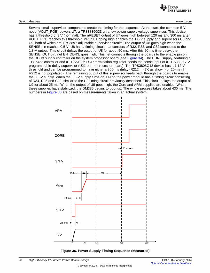
Several small supervisor components create the timing for the sequence. At the start, the common 5-Vnode (VOUT_POE) powers U7, a TPS3839G33 ultra-low power-supply voltage supervisor. This devicehas a threshold of 3 V (nominal). The nRESET output of U7 goes high between 120 ms and 300 ms afterVOUT_POE reaches this threshold. nRESET going high enables the 1.8-V supply and supervisors U8 andU9, both of which are TPS3897-adjustable supervisor circuits. The output of U8 goes high when theSENSE pin reaches 0.5 V. U8 has a timing circuit that consists of R32, R33, and C32 connected to the1.8-V output. This circuit delays the output of U8 for about 50 ms. After this 50-ms time delay, theSENSE_OUT pin, net EN_DDR3, goes high. This net connects through the boards to the enable pin onthe DDR3 supply controller on the system processor board (see Figure 34). The DDR3 supply, featuring aTPS5432 controller and a TPS51206 DDR termination regulator, feeds the sense input of a TPS3808G12programmable-delay supervisor (U21 on the processor board). The TPS3808G12 device has a 1.12-Vthreshold and can be programmed to have either a 300-ms delay (R212 = 47K as shown) or 20-ms (ifR212 is not populated). The remaining output of this supervisor feeds back through the boards to enablethe 3.3-V supply. When the 3.3-V supply turns on, U9 on the power module has a timing circuit consistingof R34, R35 and C33, similar to the U8 timing circuit previously described. This circuit delays the output ofU9 for about 25 ms. When the output of U9 goes high, the Core and ARM supplies are enabled. Whenthese supplies have stabilized, the DM385 begins to boot up. The whole process takes about 430 ms. Thenumbers in Figure 36 are based on measurements taken in an actual system.
Figure 36. Power Supply Timing Sequence (Measured)
20 High-Efficiency IP Camera Power Module Design TIDU188–January 2014Submit Documentation Feedback
Copyright © 2014, Texas Instruments Incorporated
www.ti.com System Performance
2.3 Other CircuitsThere are several other circuits that make up the power module that provide specific peripheral functionsfor the DM385 IP Camera Reference Design. The following sections list these circuits.
2.3.1 RS485 InterfaceMany security cameras are controlled by an RS485 two-wire serial interface. In this system, twoSN74AVC2T45 level translators convert the 1.8-V signal level on the DM385 to the 3.3-V IO required bythe SN65HVD11 RS485 transceiver. The output is on J5 which is shared with the alarm.
2.3.2 Alarm InterfaceThe alarm Interface has an optically-isolated output and two optically-isolated inputs. The optically-isolatedinputs and output provide a means for the DM385 to send or receive interrupts to and from another deviceor camera.
2.3.3 Indicator LightsThe indicator lights are LEDs and associated power switches to indicate power ON, system errors, 1000-G Ethernet connection, or a LAN event.
2.3.4 TV OutputThe TV output drives a BNC connector on the camera housing which allows the camera to be used as astandard definition security camera in an existing security system. The SD output is driven by an OPA360device which is a low-power OPAMP designed specifically for driving a video output.
2.3.5 IRIS DriverTwo PWM signals from the DM385 control the IRIS output. The output is driven by a an LMV722 low-noise operational amplifier (op-amp).
2.3.6 Earphone JackThe earphone jack is the audio output for the camera.
2.3.7 Battery ChargerA Lithium-Ion battery charger is included in the design for applications where a backup battery is desired.In the DM385 IP Camera Reference Design, this function is not used and the circuit is bypassed in thepower module.
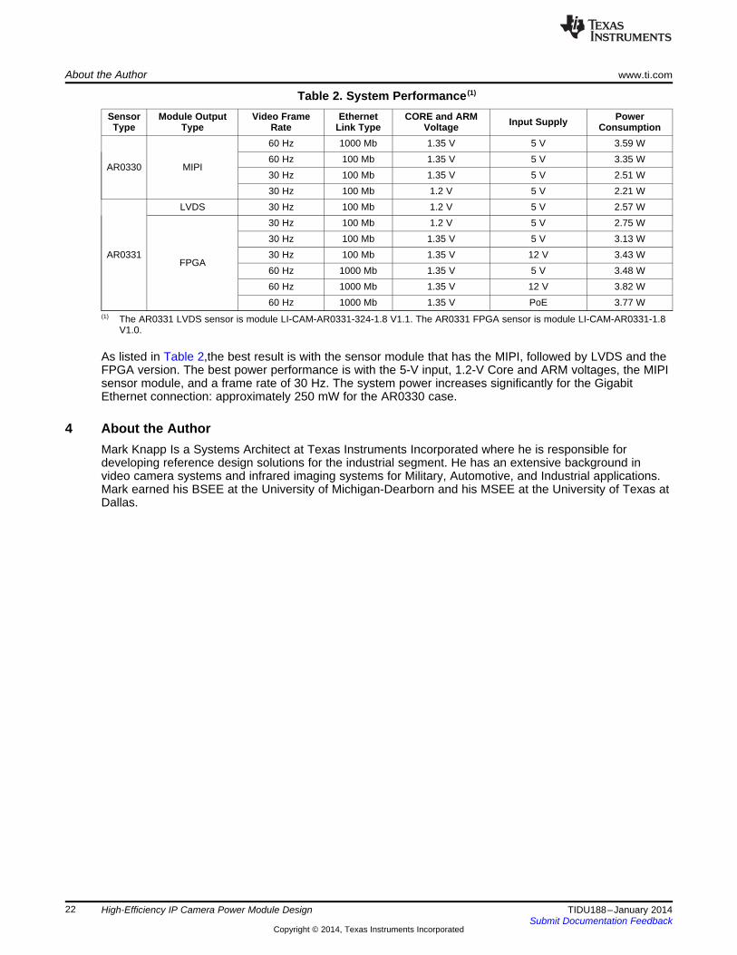
3 System PerformanceSystem power consumption is the ultimate measure of a power supply design. For the DM385 IP NetCamera, the power consumption is very low although it is a function of the chosen image sensor moduleand the frame rate of the video. Table 2 lists data received from three different image sensor modules, twodifferent frame rates (30 Hz and 60Hz), and with the Core and ARM voltage set for 1.2-V for some of the30-Hz tests. In all cases, the IP camera streams three video streams, 1080p H.264, 1080p MPEG4, andD1 30Hz. The image sensor modules are available from Leopard Imaging. These image modules arebased on the Aptina AR0330 and AR0331 Imagers.
21TIDU188–January 2014 High-Efficiency IP Camera Power Module DesignSubmit Documentation Feedback
Copyright © 2014, Texas Instruments Incorporated
About the Author www.ti.com
Table 2. System Performance (1)
Sensor Module Output Video Frame Ethernet CORE and ARM PowerInput SupplyType Type Rate Link Type Voltage Consumption60 Hz 1000 Mb 1.35 V 5 V 3.59 W60 Hz 100 Mb 1.35 V 5 V 3.35 W
AR0330 MIPI30 Hz 100 Mb 1.35 V 5 V 2.51 W30 Hz 100 Mb 1.2 V 5 V 2.21 W
LVDS 30 Hz 100 Mb 1.2 V 5 V 2.57 W30 Hz 100 Mb 1.2 V 5 V 2.75 W30 Hz 100 Mb 1.35 V 5 V 3.13 W
AR0331 30 Hz 100 Mb 1.35 V 12 V 3.43 WFPGA
60 Hz 1000 Mb 1.35 V 5 V 3.48 W60 Hz 1000 Mb 1.35 V 12 V 3.82 W60 Hz 1000 Mb 1.35 V PoE 3.77 W
(1) The AR0331 LVDS sensor is module LI-CAM-AR0331-324-1.8 V1.1. The AR0331 FPGA sensor is module LI-CAM-AR0331-1.8V1.0.
As listed in Table 2,the best result is with the sensor module that has the MIPI, followed by LVDS and theFPGA version. The best power performance is with the 5-V input, 1.2-V Core and ARM voltages, the MIPIsensor module, and a frame rate of 30 Hz. The system power increases significantly for the GigabitEthernet connection: approximately 250 mW for the AR0330 case.
4 About the AuthorMark Knapp Is a Systems Architect at Texas Instruments Incorporated where he is responsible fordeveloping reference design solutions for the industrial segment. He has an extensive background invideo camera systems and infrared imaging systems for Military, Automotive, and Industrial applications.Mark earned his BSEE at the University of Michigan-Dearborn and his MSEE at the University of Texas atDallas.
22 High-Efficiency IP Camera Power Module Design TIDU188–January 2014Submit Documentation Feedback
Copyright © 2014, Texas Instruments Incorporated
EVALUATION BOARD/KIT/MODULE (EVM) ADDITIONAL TERMSTexas Instruments (TI) provides the enclosed Evaluation Board/Kit/Module (EVM) under the following conditions:The user assumes all responsibility and liability for proper and safe handling of the goods. Further, the user indemnifies TI from all claimsarising from the handling or use of the goods.Should this evaluation board/kit not meet the specifications indicated in the User’s Guide, the board/kit may be returned within 30 days fromthe date of delivery for a full refund. THE FOREGOING LIMITED WARRANTY IS THE EXCLUSIVE WARRANTY MADE BY SELLER TOBUYER AND IS IN LIEU OF ALL OTHER WARRANTIES, EXPRESSED, IMPLIED, OR STATUTORY, INCLUDING ANY WARRANTY OFMERCHANTABILITY OR FITNESS FOR ANY PARTICULAR PURPOSE. EXCEPT TO THE EXTENT OF THE INDEMNITY SET FORTHABOVE, NEITHER PARTY SHALL BE LIABLE TO THE OTHER FOR ANY INDIRECT, SPECIAL, INCIDENTAL, OR CONSEQUENTIALDAMAGES.Please read the User's Guide and, specifically, the Warnings and Restrictions notice in the User's Guide prior to handling the product. Thisnotice contains important safety information about temperatures and voltages. For additional information on TI's environmental and/or safetyprograms, please visit www.ti.com/esh or contact TI.No license is granted under any patent right or other intellectual property right of TI covering or relating to any machine, process, orcombination in which such TI products or services might be or are used. TI currently deals with a variety of customers for products, andtherefore our arrangement with the user is not exclusive. TI assumes no liability for applications assistance, customer product design,software performance, or infringement of patents or services described herein.
REGULATORY COMPLIANCE INFORMATIONAs noted in the EVM User’s Guide and/or EVM itself, this EVM and/or accompanying hardware may or may not be subject to the FederalCommunications Commission (FCC) and Industry Canada (IC) rules.For EVMs not subject to the above rules, this evaluation board/kit/module is intended for use for ENGINEERING DEVELOPMENT,DEMONSTRATION OR EVALUATION PURPOSES ONLY and is not considered by TI to be a finished end product fit for general consumeruse. It generates, uses, and can radiate radio frequency energy and has not been tested for compliance with the limits of computingdevices pursuant to part 15 of FCC or ICES-003 rules, which are designed to provide reasonable protection against radio frequencyinterference. Operation of the equipment may cause interference with radio communications, in which case the user at his own expense willbe required to take whatever measures may be required to correct this interference.General Statement for EVMs including a radioUser Power/Frequency Use Obligations: This radio is intended for development/professional use only in legally allocated frequency andpower limits. Any use of radio frequencies and/or power availability of this EVM and its development application(s) must comply with locallaws governing radio spectrum allocation and power limits for this evaluation module. It is the user’s sole responsibility to only operate thisradio in legally acceptable frequency space and within legally mandated power limitations. Any exceptions to this are strictly prohibited andunauthorized by Texas Instruments unless user has obtained appropriate experimental/development licenses from local regulatoryauthorities, which is responsibility of user including its acceptable authorization.
For EVMs annotated as FCC – FEDERAL COMMUNICATIONS COMMISSION Part 15 Compliant
CautionThis device complies with part 15 of the FCC Rules. Operation is subject to the following two conditions: (1) This device may not causeharmful interference, and (2) this device must accept any interference received, including interference that may cause undesired operation.Changes or modifications not expressly approved by the party responsible for compliance could void the user's authority to operate theequipment.
FCC Interference Statement for Class A EVM devicesThis equipment has been tested and found to comply with the limits for a Class A digital device, pursuant to part 15 of the FCC Rules.These limits are designed to provide reasonable protection against harmful interference when the equipment is operated in a commercialenvironment. This equipment generates, uses, and can radiate radio frequency energy and, if not installed and used in accordance with theinstruction manual, may cause harmful interference to radio communications. Operation of this equipment in a residential area is likely tocause harmful interference in which case the user will be required to correct the interference at his own expense.
FCC Interference Statement for Class B EVM devicesThis equipment has been tested and found to comply with the limits for a Class B digital device, pursuant to part 15 of the FCC Rules.These limits are designed to provide reasonable protection against harmful interference in a residential installation. This equipmentgenerates, uses and can radiate radio frequency energy and, if not installed and used in accordance with the instructions, may causeharmful interference to radio communications. However, there is no guarantee that interference will not occur in a particular installation. Ifthis equipment does cause harmful interference to radio or television reception, which can be determined by turning the equipment off andon, the user is encouraged to try to correct the interference by one or more of the following measures:
• Reorient or relocate the receiving antenna.• Increase the separation between the equipment and receiver.• Connect the equipment into an outlet on a circuit different from that to which the receiver is connected.• Consult the dealer or an experienced radio/TV technician for help.
For EVMs annotated as IC – INDUSTRY CANADA Compliant
This Class A or B digital apparatus complies with Canadian ICES-003.Changes or modifications not expressly approved by the party responsible for compliance could void the user’s authority to operate theequipment.
Concerning EVMs including radio transmitters
This device complies with Industry Canada licence-exempt RSS standard(s). Operation is subject to the following two conditions: (1) thisdevice may not cause interference, and (2) this device must accept any interference, including interference that may cause undesiredoperation of the device.
Concerning EVMs including detachable antennasUnder Industry Canada regulations, this radio transmitter may only operate using an antenna of a type and maximum (or lesser) gainapproved for the transmitter by Industry Canada. To reduce potential radio interference to other users, the antenna type and its gain shouldbe so chosen that the equivalent isotropically radiated power (e.i.r.p.) is not more than that necessary for successful communication.
This radio transmitter has been approved by Industry Canada to operate with the antenna types listed in the user guide with the maximumpermissible gain and required antenna impedance for each antenna type indicated. Antenna types not included in this list, having a gaingreater than the maximum gain indicated for that type, are strictly prohibited for use with this device.
Cet appareil numérique de la classe A ou B est conforme à la norme NMB-003 du Canada.
Les changements ou les modifications pas expressément approuvés par la partie responsable de la conformité ont pu vider l’autorité del'utilisateur pour actionner l'équipement.
Concernant les EVMs avec appareils radio
Le présent appareil est conforme aux CNR d'Industrie Canada applicables aux appareils radio exempts de licence. L'exploitation estautorisée aux deux conditions suivantes : (1) l'appareil ne doit pas produire de brouillage, et (2) l'utilisateur de l'appareil doit accepter toutbrouillage radioélectrique subi, même si le brouillage est susceptible d'en compromettre le fonctionnement.
Concernant les EVMs avec antennes détachables
Conformément à la réglementation d'Industrie Canada, le présent émetteur radio peut fonctionner avec une antenne d'un type et d'un gainmaximal (ou inférieur) approuvé pour l'émetteur par Industrie Canada. Dans le but de réduire les risques de brouillage radioélectrique àl'intention des autres utilisateurs, il faut choisir le type d'antenne et son gain de sorte que la puissance isotrope rayonnée équivalente(p.i.r.e.) ne dépasse pas l'intensité nécessaire à l'établissement d'une communication satisfaisante.
Le présent émetteur radio a été approuvé par Industrie Canada pour fonctionner avec les types d'antenne énumérés dans le manueld’usage et ayant un gain admissible maximal et l'impédance requise pour chaque type d'antenne. Les types d'antenne non inclus danscette liste, ou dont le gain est supérieur au gain maximal indiqué, sont strictement interdits pour l'exploitation de l'émetteur.
SPACER
SPACER
SPACER
SPACER
SPACER
SPACER
SPACER
SPACER
【【Important Notice for Users of EVMs for RF Products in Japan】】This development kit is NOT certified as Confirming to Technical Regulations of Radio Law of Japan
If you use this product in Japan, you are required by Radio Law of Japan to follow the instructions below with respect to this product:1. Use this product in a shielded room or any other test facility as defined in the notification #173 issued by Ministry of Internal Affairs and
Communications on March 28, 2006, based on Sub-section 1.1 of Article 6 of the Ministry’s Rule for Enforcement of Radio Law ofJapan,
2. Use this product only after you obtained the license of Test Radio Station as provided in Radio Law of Japan with respect to thisproduct, or
3. Use of this product only after you obtained the Technical Regulations Conformity Certification as provided in Radio Law of Japan withrespect to this product. Also, please do not transfer this product, unless you give the same notice above to the transferee. Please notethat if you could not follow the instructions above, you will be subject to penalties of Radio Law of Japan.
Texas Instruments Japan Limited(address) 24-1, Nishi-Shinjuku 6 chome, Shinjuku-ku, Tokyo, Japan
http://www.tij.co.jp
【無線電波を送信する製品の開発キットをお使いになる際の注意事項】
本開発キットは技術基準適合証明を受けておりません。
本製品のご使用に際しては、電波法遵守のため、以下のいずれかの措置を取っていただく必要がありますのでご注意ください。1. 電波法施行規則第6条第1項第1号に基づく平成18年3月28日総務省告示第173号で定められた電波暗室等の試験設備でご使用いただく。2. 実験局の免許を取得後ご使用いただく。3. 技術基準適合証明を取得後ご使用いただく。
なお、本製品は、上記の「ご使用にあたっての注意」を譲渡先、移転先に通知しない限り、譲渡、移転できないものとします。
上記を遵守頂けない場合は、電波法の罰則が適用される可能性があることをご留意ください。
日本テキサス・インスツルメンツ株式会社東京都新宿区西新宿6丁目24番1号西新宿三井ビルhttp://www.tij.co.jp
SPACER
SPACER
SPACER
SPACER
SPACER
SPACER
SPACER
SPACER
SPACER
SPACER
SPACER
SPACER
SPACER
SPACER
SPACER
SPACER
SPACER
EVALUATION BOARD/KIT/MODULE (EVM)WARNINGS, RESTRICTIONS AND DISCLAIMERS
For Feasibility Evaluation Only, in Laboratory/Development Environments. Unless otherwise indicated, this EVM is not a finishedelectrical equipment and not intended for consumer use. It is intended solely for use for preliminary feasibility evaluation inlaboratory/development environments by technically qualified electronics experts who are familiar with the dangers and application risksassociated with handling electrical mechanical components, systems and subsystems. It should not be used as all or part of a finished endproduct.
Your Sole Responsibility and Risk. You acknowledge, represent and agree that:1. You have unique knowledge concerning Federal, State and local regulatory requirements (including but not limited to Food and Drug
Administration regulations, if applicable) which relate to your products and which relate to your use (and/or that of your employees,affiliates, contractors or designees) of the EVM for evaluation, testing and other purposes.
2. You have full and exclusive responsibility to assure the safety and compliance of your products with all such laws and other applicableregulatory requirements, and also to assure the safety of any activities to be conducted by you and/or your employees, affiliates,contractors or designees, using the EVM. Further, you are responsible to assure that any interfaces (electronic and/or mechanical)between the EVM and any human body are designed with suitable isolation and means to safely limit accessible leakage currents tominimize the risk of electrical shock hazard.
3. Since the EVM is not a completed product, it may not meet all applicable regulatory and safety compliance standards (such as UL,CSA, VDE, CE, RoHS and WEEE) which may normally be associated with similar items. You assume full responsibility to determineand/or assure compliance with any such standards and related certifications as may be applicable. You will employ reasonablesafeguards to ensure that your use of the EVM will not result in any property damage, injury or death, even if the EVM should fail toperform as described or expected.
4. You will take care of proper disposal and recycling of the EVM’s electronic components and packing materials.
Certain Instructions. It is important to operate this EVM within TI’s recommended specifications and environmental considerations per theuser guidelines. Exceeding the specified EVM ratings (including but not limited to input and output voltage, current, power, andenvironmental ranges) may cause property damage, personal injury or death. If there are questions concerning these ratings please contacta TI field representative prior to connecting interface electronics including input power and intended loads. Any loads applied outside of thespecified output range may result in unintended and/or inaccurate operation and/or possible permanent damage to the EVM and/orinterface electronics. Please consult the EVM User's Guide prior to connecting any load to the EVM output. If there is uncertainty as to theload specification, please contact a TI field representative. During normal operation, some circuit components may have case temperaturesgreater than 60°C as long as the input and output are maintained at a normal ambient operating temperature. These components includebut are not limited to linear regulators, switching transistors, pass transistors, and current sense resistors which can be identified using theEVM schematic located in the EVM User's Guide. When placing measurement probes near these devices during normal operation, pleasebe aware that these devices may be very warm to the touch. As with all electronic evaluation tools, only qualified personnel knowledgeablein electronic measurement and diagnostics normally found in development environments should use these EVMs.
Agreement to Defend, Indemnify and Hold Harmless. You agree to defend, indemnify and hold TI, its licensors and their representativesharmless from and against any and all claims, damages, losses, expenses, costs and liabilities (collectively, "Claims") arising out of or inconnection with any use of the EVM that is not in accordance with the terms of the agreement. This obligation shall apply whether Claimsarise under law of tort or contract or any other legal theory, and even if the EVM fails to perform as described or expected.
Safety-Critical or Life-Critical Applications. If you intend to evaluate the components for possible use in safety critical applications (suchas life support) where a failure of the TI product would reasonably be expected to cause severe personal injury or death, such as deviceswhich are classified as FDA Class III or similar classification, then you must specifically notify TI of such intent and enter into a separateAssurance and Indemnity Agreement.
Mailing Address: Texas Instruments, Post Office Box 655303, Dallas, Texas 75265Copyright © 2014, Texas Instruments Incorporated
IMPORTANT NOTICE FOR TI REFERENCE DESIGNSTexas Instruments Incorporated ("TI") reference designs are solely intended to assist designers (“Buyers”) who are developing systems thatincorporate TI semiconductor products (also referred to herein as “components”). Buyer understands and agrees that Buyer remainsresponsible for using its independent analysis, evaluation and judgment in designing Buyer’s systems and products.TI reference designs have been created using standard laboratory conditions and engineering practices. TI has not conducted anytesting other than that specifically described in the published documentation for a particular reference design. TI may makecorrections, enhancements, improvements and other changes to its reference designs.Buyers are authorized to use TI reference designs with the TI component(s) identified in each particular reference design and to modify thereference design in the development of their end products. HOWEVER, NO OTHER LICENSE, EXPRESS OR IMPLIED, BY ESTOPPELOR OTHERWISE TO ANY OTHER TI INTELLECTUAL PROPERTY RIGHT, AND NO LICENSE TO ANY THIRD PARTY TECHNOLOGYOR INTELLECTUAL PROPERTY RIGHT, IS GRANTED HEREIN, including but not limited to any patent right, copyright, mask work right,or other intellectual property right relating to any combination, machine, or process in which TI components or services are used.Information published by TI regarding third-party products or services does not constitute a license to use such products or services, or awarranty or endorsement thereof. Use of such information may require a license from a third party under the patents or other intellectualproperty of the third party, or a license from TI under the patents or other intellectual property of TI.TI REFERENCE DESIGNS ARE PROVIDED "AS IS". TI MAKES NO WARRANTIES OR REPRESENTATIONS WITH REGARD TO THEREFERENCE DESIGNS OR USE OF THE REFERENCE DESIGNS, EXPRESS, IMPLIED OR STATUTORY, INCLUDING ACCURACY ORCOMPLETENESS. TI DISCLAIMS ANY WARRANTY OF TITLE AND ANY IMPLIED WARRANTIES OF MERCHANTABILITY, FITNESSFOR A PARTICULAR PURPOSE, QUIET ENJOYMENT, QUIET POSSESSION, AND NON-INFRINGEMENT OF ANY THIRD PARTYINTELLECTUAL PROPERTY RIGHTS WITH REGARD TO TI REFERENCE DESIGNS OR USE THEREOF. TI SHALL NOT BE LIABLEFOR AND SHALL NOT DEFEND OR INDEMNIFY BUYERS AGAINST ANY THIRD PARTY INFRINGEMENT CLAIM THAT RELATES TOOR IS BASED ON A COMBINATION OF COMPONENTS PROVIDED IN A TI REFERENCE DESIGN. IN NO EVENT SHALL TI BELIABLE FOR ANY ACTUAL, SPECIAL, INCIDENTAL, CONSEQUENTIAL OR INDIRECT DAMAGES, HOWEVER CAUSED, ON ANYTHEORY OF LIABILITY AND WHETHER OR NOT TI HAS BEEN ADVISED OF THE POSSIBILITY OF SUCH DAMAGES, ARISING INANY WAY OUT OF TI REFERENCE DESIGNS OR BUYER’S USE OF TI REFERENCE DESIGNS.TI reserves the right to make corrections, enhancements, improvements and other changes to its semiconductor products and services perJESD46, latest issue, and to discontinue any product or service per JESD48, latest issue. Buyers should obtain the latest relevantinformation before placing orders and should verify that such information is current and complete. All semiconductor products are soldsubject to TI’s terms and conditions of sale supplied at the time of order acknowledgment.TI warrants performance of its components to the specifications applicable at the time of sale, in accordance with the warranty in TI’s termsand conditions of sale of semiconductor products. Testing and other quality control techniques for TI components are used to the extent TIdeems necessary to support this warranty. Except where mandated by applicable law, testing of all parameters of each component is notnecessarily performed.TI assumes no liability for applications assistance or the design of Buyers’ products. Buyers are responsible for their products andapplications using TI components. To minimize the risks associated with Buyers’ products and applications, Buyers should provideadequate design and operating safeguards.Reproduction of significant portions of TI information in TI data books, data sheets or reference designs is permissible only if reproduction iswithout alteration and is accompanied by all associated warranties, conditions, limitations, and notices. TI is not responsible or liable forsuch altered documentation. Information of third parties may be subject to additional restrictions.Buyer acknowledges and agrees that it is solely responsible for compliance with all legal, regulatory and safety-related requirementsconcerning its products, and any use of TI components in its applications, notwithstanding any applications-related information or supportthat may be provided by TI. Buyer represents and agrees that it has all the necessary expertise to create and implement safeguards thatanticipate dangerous failures, monitor failures and their consequences, lessen the likelihood of dangerous failures and take appropriateremedial actions. Buyer will fully indemnify TI and its representatives against any damages arising out of the use of any TI components inBuyer’s safety-critical applications.In some cases, TI components may be promoted specifically to facilitate safety-related applications. With such components, TI’s goal is tohelp enable customers to design and create their own end-product solutions that meet applicable functional safety standards andrequirements. Nonetheless, such components are subject to these terms.No TI components are authorized for use in FDA Class III (or similar life-critical medical equipment) unless authorized officers of the partieshave executed an agreement specifically governing such use.Only those TI components that TI has specifically designated as military grade or “enhanced plastic” are designed and intended for use inmilitary/aerospace applications or environments. Buyer acknowledges and agrees that any military or aerospace use of TI components thathave not been so designated is solely at Buyer's risk, and Buyer is solely responsible for compliance with all legal and regulatoryrequirements in connection with such use.TI has specifically designated certain components as meeting ISO/TS16949 requirements, mainly for automotive use. In any case of use ofnon-designated products, TI will not be responsible for any failure to meet ISO/TS16949.
Mailing Address: Texas Instruments, Post Office Box 655303, Dallas, Texas 75265Copyright © 2014, Texas Instruments Incorporated