Embed Size (px)
Citation preview
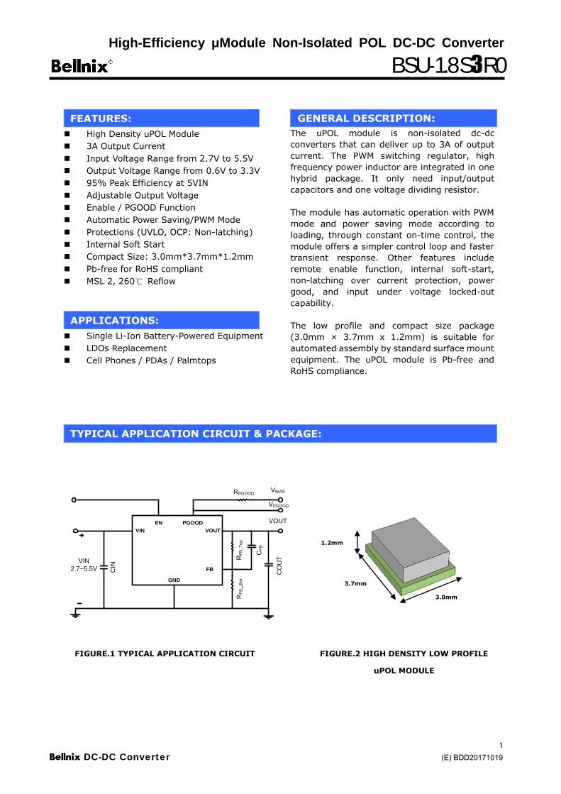
High-Efficiency μModule Non-Isolated POL DC-DC Converter
BSU-1.8S3R0
Bellnix DC-DC Converter 1
(E) BDD20171019
FEATURES:
High Density uPOL Module
3A Output Current
Input Voltage Range from 2.7V to 5.5V
Output Voltage Range from 0.6V to 3.3V
95% Peak Efficiency at 5VIN
Adjustable Output Voltage
Enable / PGOOD Function
Automatic Power Saving/PWM Mode
Protections (UVLO, OCP: Non-latching)
Internal Soft Start
Compact Size: 3.0mm*3.7mm*1.2mm
Pb-free for RoHS compliant
MSL 2, 260℃ Reflow
APPLICATIONS:
Single Li-Ion Battery-Powered Equipment
LDOs Replacement
Cell Phones / PDAs / Palmtops
GENERAL DESCRIPTION:
The uPOL module is non-isolated dc-dc
converters that can deliver up to 3A of output
current. The PWM switching regulator, high
frequency power inductor are integrated in one
hybrid package. It only need input/output
capacitors and one voltage dividing resistor.
The module has automatic operation with PWM
mode and power saving mode according to
loading, through constant on-time control, the
module offers a simpler control loop and faster
transient response. Other features include
remote enable function, internal soft-start,
non-latching over current protection, power
good, and input under voltage locked-out
capability.
The low profile and compact size package
(3.0mm × 3.7mm x 1.2mm) is suitable for
automated assembly by standard surface mount
equipment. The uPOL module is Pb-free and
RoHS compliance.
TYPICAL APPLICATION CIRCUIT & PACKAGE:
EN PGOOD
VOUT
FB
GND
VIN
VBIAS
CIN
VOUT
VIN
2.7~5.5V
RF
B_
To
pR
FB_
Bo
t
CF
B
CO
UT
VPGOOD
RPGOOD
FIGURE.1 TYPICAL APPLICATION CIRCUIT FIGURE.2 HIGH DENSITY LOW PROFILE
uPOL MODULE
3.7mm
3.0mm
1.2mm
High-Efficiency μModule Non-Isolated POL DC-DC Converter
BSU-1.8S3R0
Bellnix DC-DC Converter 2
(E) BDD20171019
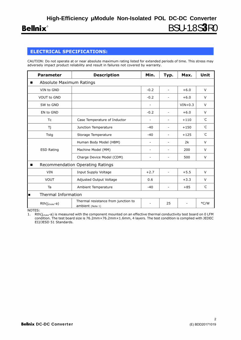
ELECTRICAL SPECIFICATIONS:
CAUTION: Do not operate at or near absolute maximum rating listed for extended periods of time. This stress may adversely impact product reliability and result in failures not covered by warranty.
NOTES: 1. Rth(jchoke-a) is measured with the component mounted on an effective thermal conductivity test board on 0 LFM
condition. The test board size is 76.2mm× 76.2mm× 1.6mm, 4 layers. The test condition is complied with JEDEC EIJ/JESD 51 Standards.
Parameter Description Min. Typ. Max. Unit
Absolute Maximum Ratings
VIN to GND -0.2 - +6.0 V
VOUT to GND -0.2 - +6.0 V
SW to GND - VIN+0.3 V
EN to GND -0.2 - +6.0 V
Tc Case Temperature of Inductor - - +110 °C
Tj Junction Temperature -40 - +150 °C
Tstg Storage Temperature -40 - +125 °C
ESD Rating
Human Body Model (HBM) - - 2k V
Machine Model (MM) - - 200 V
Charge Device Model (CDM) - - 500 V
Recommendation Operating Ratings
VIN Input Supply Voltage +2.7 - +5.5 V
VOUT Adjusted Output Voltage 0.6 +3.3 V
Ta Ambient Temperature -40 - +85 °C
Thermal Information
Rth(jchoke-a) Thermal resistance from junction to
ambient (Note 1) - 25 - °C/W
High-Efficiency μModule Non-Isolated POL DC-DC Converter
BSU-1.8S3R0
Bellnix DC-DC Converter 3
(E) BDD20171019
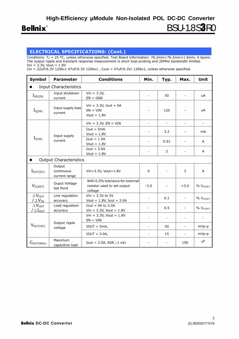
ELECTRICAL SPECIFICATIONS: (Cont.) Conditions: TA = 25 ºC, unless otherwise specified. Test Board Information: 76.2mm× 76.2mm× 1.6mm, 4 layers. The output ripple and transient response measurement is short loop probing and 20MHz bandwidth limited. Vin = 3.3V, Vout = 1.8V Cin = 22uF/6.3V 1206×1 47uF/6.3V 1206x1 , Cout = 47uF/6.3V/ 1206x1, unless otherwise specified.
Symbol Parameter Conditions Min. Typ. Max. Unit
Input Characteristics
ISD(IN)Input shutdown
current
Vin = 3.3V,
EN = GND - 50 - uA
IQ(IN)Input supply bias
current
Vin = 3.3V, Iout = 0A
EN = VIN
Vout = 1.8V
- 120 - uA
IS(IN) Input supply
current
Vin = 3.3V, EN = VIN - - - -
Iout = 5mA
Vout = 1.8V - 3.2 - mA
Iout = 1.5A
Vout = 1.8V - 0.91 - A
Iout = 3.0A
Vout = 1.8V - 2 - A
Output Characteristics
IOUT(DC) Output
continuous
current range
Vin=3.3V, Vout=1.8V 0 - 3 A
VO(SET) Ouput Voltage
Set Point
With 0.5% tolerance for external
resistor used to set output
voltage
-3.0 - +3.0 % VO(SET)
ΔVOUT
/ΔVIN Line regulation
accuracy
Vin = 3.3V to 5V
Vout = 1.8V, Iout = 3.0A - 0.1 - % VO(SET)
ΔVOUT
/ΔIOUT Load regulation
accuracy
Iout = 0A to 3.0A
Vin = 3.3V, Vout = 1.8V - 0.5 - % VO(SET)
VOUT(AC) Output ripple
voltage
Vin = 3.3V, Vout = 1.8V
EN = VIN - - - -
IOUT = 5mA, - 50 - mVp-p
IOUT = 3.0A, - 15 - mVp-p
COUT(MAX)Maximum
capacitive load Iout = 3.0A, ESR≧1 m - - 150 uF
High-Efficiency μModule Non-Isolated POL DC-DC Converter
BSU-1.8S3R0
Bellnix DC-DC Converter 4
(E) BDD20171019
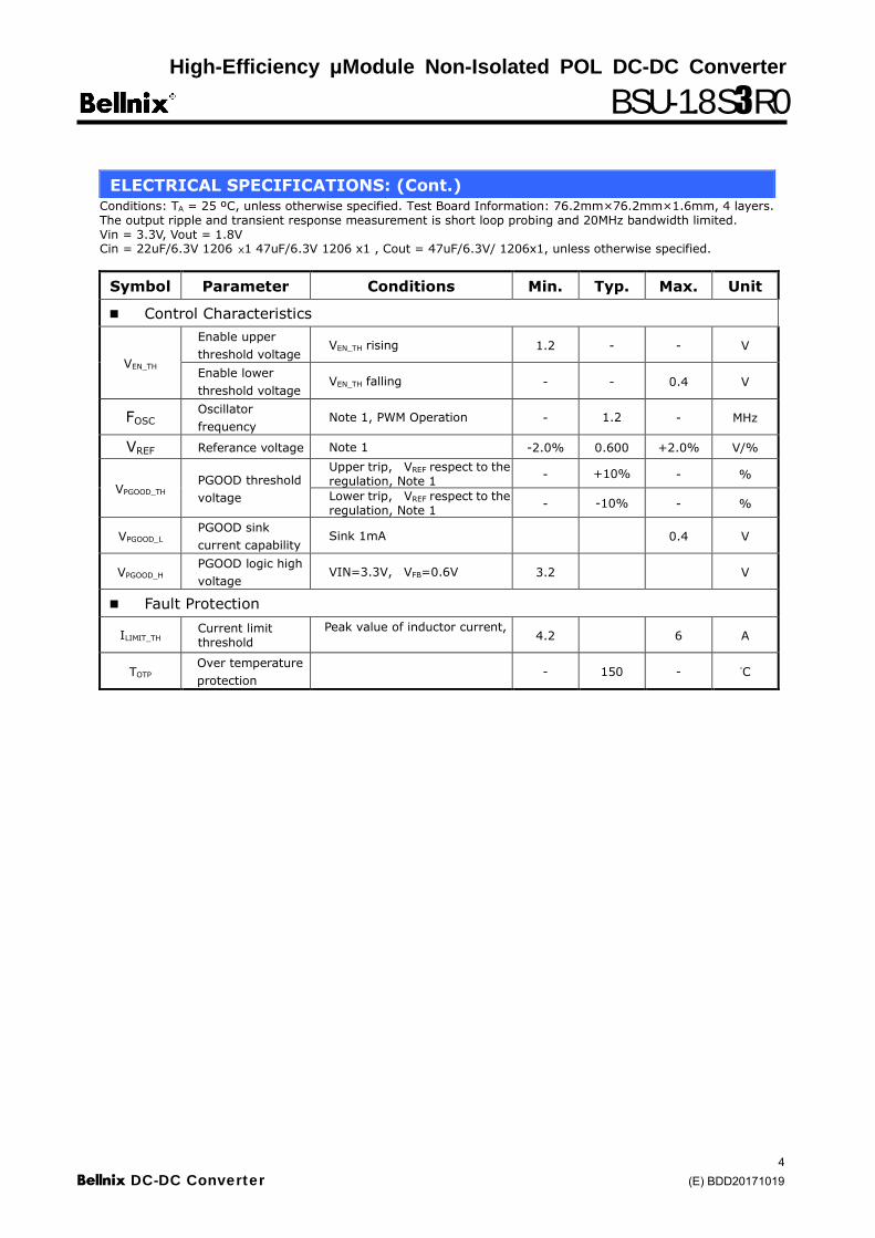
ELECTRICAL SPECIFICATIONS: (Cont.) Conditions: TA = 25 ºC, unless otherwise specified. Test Board Information: 76.2mm× 76.2mm× 1.6mm, 4 layers. The output ripple and transient response measurement is short loop probing and 20MHz bandwidth limited. Vin = 3.3V, Vout = 1.8V Cin = 22uF/6.3V 1206 ×1 47uF/6.3V 1206 x1 , Cout = 47uF/6.3V/ 1206x1, unless otherwise specified.
Symbol Parameter Conditions Min. Typ. Max. Unit
Control Characteristics
VEN_TH
Enable upper
threshold voltage VEN_TH rising 1.2 - - V
Enable lower
threshold voltage VEN_TH falling - - 0.4 V
FOSC Oscillator
frequency Note 1, PWM Operation - 1.2 - MHz
VREF Referance voltage Note 1 -2.0% 0.600 +2.0% V/%
VPGOOD_TH PGOOD threshold
voltage
Upper trip, VREF respect to the regulation, Note 1
- +10% - %
Lower trip, VREF respect to the regulation, Note 1
- -10% - %
VPGOOD_L PGOOD sink
current capability Sink 1mA 0.4 V
VPGOOD_H PGOOD logic high
voltage VIN=3.3V, VFB=0.6V 3.2 V
Fault Protection
ILIMIT_TH Current limit threshold
Peak value of inductor current, 4.2 6 A
TOTP Over temperature
protection - 150 - °C
High-Efficiency μModule Non-Isolated POL DC-DC Converter
BSU-1.8S3R0
Bellnix DC-DC Converter 5
(E) BDD20171019
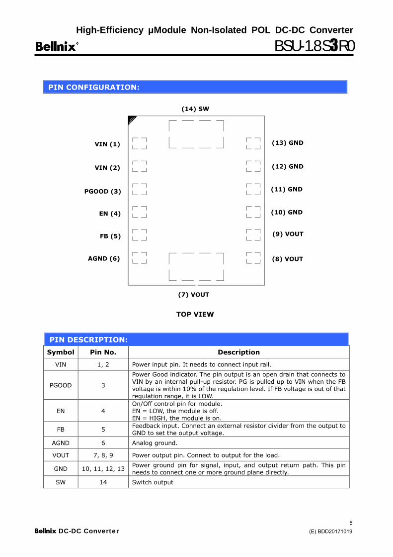
PIN CONFIGURATION:
TOP VIEW
VIN (1)
(9) VOUT
(7) VOUT
VIN (2)
EN (4)
FB (5)
AGND (6)
PGOOD (3) (11) GND
(8) VOUT
(10) GND
(12) GND
(13) GND
(14) SW
PIN DESCRIPTION:
Symbol Pin No. Description
VIN 1, 2 Power input pin. It needs to connect input rail.
PGOOD 3
Power Good indicator. The pin output is an open drain that connects to VIN by an internal pull-up resistor. PG is pulled up to VIN when the FB voltage is within 10% of the regulation level. If FB voltage is out of that regulation range, it is LOW.
EN 4 On/Off control pin for module. EN = LOW, the module is off. EN = HIGH, the module is on.
FB 5 Feedback input. Connect an external resistor divider from the output to
GND to set the output voltage.
AGND 6 Analog ground.
VOUT 7, 8, 9 Power output pin. Connect to output for the load.
GND 10, 11, 12, 13 Power ground pin for signal, input, and output return path. This pin needs to connect one or more ground plane directly.
SW 14 Switch output
High-Efficiency μModule Non-Isolated POL DC-DC Converter
BSU-1.8S3R0
Bellnix DC-DC Converter 6
(E) BDD20171019
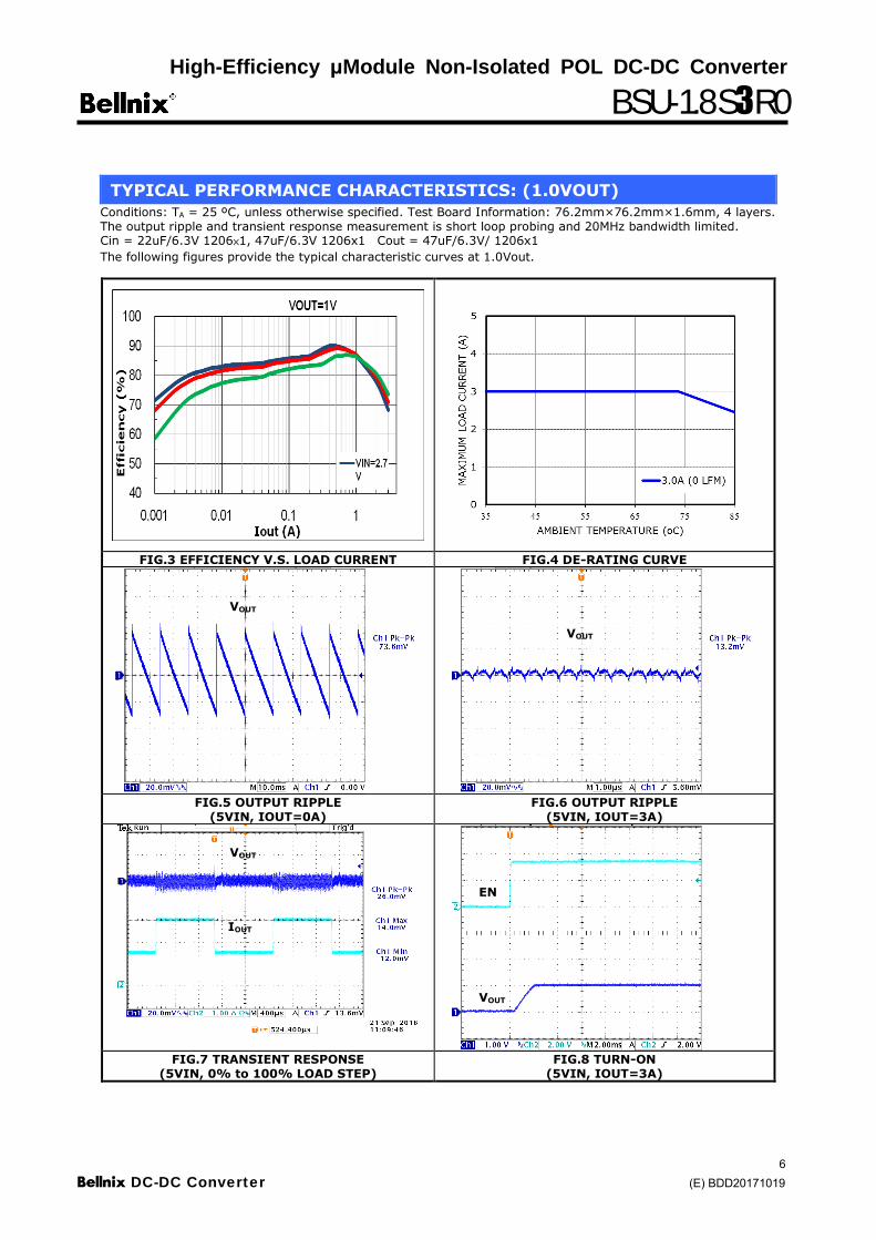
TYPICAL PERFORMANCE CHARACTERISTICS: (1.0VOUT)
Conditions: TA = 25 ºC, unless otherwise specified. Test Board Information: 76.2mm× 76.2mm× 1.6mm, 4 layers. The output ripple and transient response measurement is short loop probing and 20MHz bandwidth limited. Cin = 22uF/6.3V 1206×1, 47uF/6.3V 1206x1 Cout = 47uF/6.3V/ 1206x1
The following figures provide the typical characteristic curves at 1.0Vout.
FIG.3 EFFICIENCY V.S. LOAD CURRENT FIG.4 DE-RATING CURVE
FIG.5 OUTPUT RIPPLE (5VIN, IOUT=0A)
FIG.6 OUTPUT RIPPLE (5VIN, IOUT=3A)
FIG.7 TRANSIENT RESPONSE (5VIN, 0% to 100% LOAD STEP)
FIG.8 TURN-ON (5VIN, IOUT=3A)
VOUT
VOUT
VOUT
EN
VOUT
IOUT
High-Efficiency μModule Non-Isolated POL DC-DC Converter
BSU-1.8S3R0
Bellnix DC-DC Converter 7
(E) BDD20171019
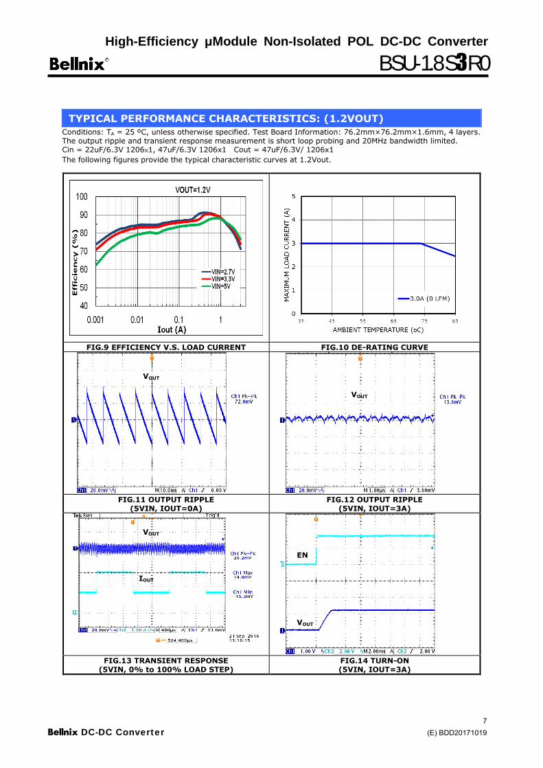
TYPICAL PERFORMANCE CHARACTERISTICS: (1.2VOUT)
Conditions: TA = 25 ºC, unless otherwise specified. Test Board Information: 76.2mm× 76.2mm× 1.6mm, 4 layers. The output ripple and transient response measurement is short loop probing and 20MHz bandwidth limited. Cin = 22uF/6.3V 1206×1, 47uF/6.3V 1206x1 Cout = 47uF/6.3V/ 1206x1
The following figures provide the typical characteristic curves at 1.2Vout.
FIG.9 EFFICIENCY V.S. LOAD CURRENT FIG.10 DE-RATING CURVE
FIG.11 OUTPUT RIPPLE (5VIN, IOUT=0A)
FIG.12 OUTPUT RIPPLE (5VIN, IOUT=3A)
FIG.13 TRANSIENT RESPONSE (5VIN, 0% to 100% LOAD STEP)
FIG.14 TURN-ON (5VIN, IOUT=3A)
VOUT
VOUT
VOUT
EN
VOUT
IOUT
High-Efficiency μModule Non-Isolated POL DC-DC Converter
BSU-1.8S3R0
Bellnix DC-DC Converter 8
(E) BDD20171019
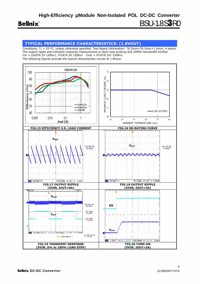
TYPICAL PERFORMANCE CHARACTERISTICS: (1.8VOUT)
Conditions: TA = 25 ºC, unless otherwise specified. Test Board Information: 76.2mm× 76.2mm× 1.6mm, 4 layers. The output ripple and transient response measurement is short loop probing and 20MHz bandwidth limited. Cin = 22uF/6.3V 1206×1, 47uF/6.3V 1206x1 Cout = 47uF/6.3V/ 1206x1
The following figures provide the typical characteristic curves at 1.8Vout.
FIG.15 EFFICIENCY V.S. LOAD CURRENT FIG.16 DE-RATING CURVE
FIG.17 OUTPUT RIPPLE (5VIN, IOUT=0A)
FIG.18 OUTPUT RIPPLE (5VIN, IOUT=3A)
FIG.19 TRANSIENT RESPONSE (5VIN, 0% to 100% LOAD STEP)
FIG.20 TURN-ON (5VIN, IOUT=3A)
VOUT
VOUT
VOUT
EN
VOUT
IOUT
High-Efficiency μModule Non-Isolated POL DC-DC Converter
BSU-1.8S3R0
Bellnix DC-DC Converter 9
(E) BDD20171019
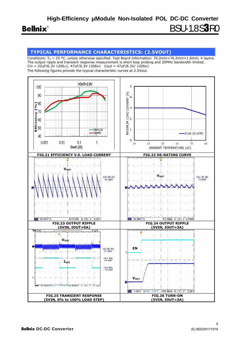
TYPICAL PERFORMANCE CHARACTERISTICS: (2.5VOUT)
Conditions: TA = 25 ºC, unless otherwise specified. Test Board Information: 76.2mm× 76.2mm× 1.6mm, 4 layers. The output ripple and transient response measurement is short loop probing and 20MHz bandwidth limited. Cin = 22uF/6.3V 1206×1, 47uF/6.3V 1206x1 Cout = 47uF/6.3V/ 1206x1
The following figures provide the typical characteristic curves at 2.5Vout.
FIG.21 EFFICIENCY V.S. LOAD CURRENT FIG.22 DE-RATING CURVE
FIG.23 OUTPUT RIPPLE (5VIN, IOUT=0A)
FIG.24 OUTPUT RIPPLE (5VIN, IOUT=3A)
FIG.25 TRANSIENT RESPONSE (5VIN, 0% to 100% LOAD STEP)
FIG.26 TURN-ON (5VIN, IOUT=3A)
VOUT
VOUT
VOUT
EN
VOUT
IOUT
High-Efficiency μModule Non-Isolated POL DC-DC Converter
BSU-1.8S3R0
Bellnix DC-DC Converter 10
(E) BDD20171019
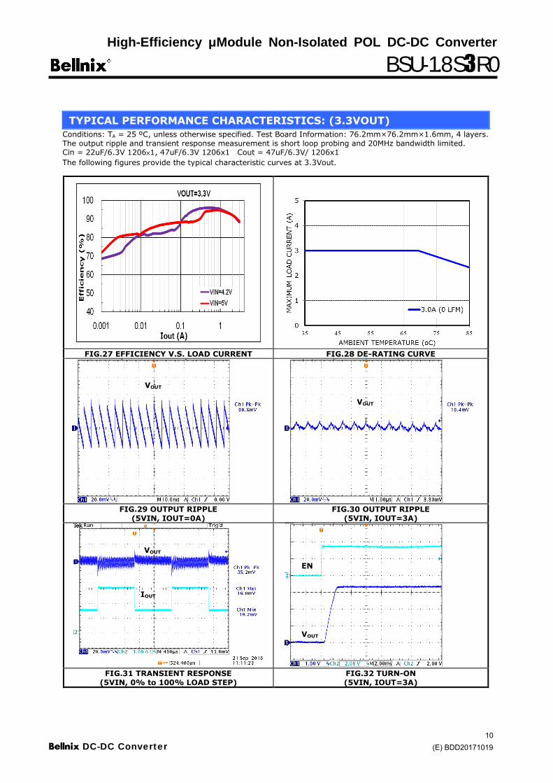
TYPICAL PERFORMANCE CHARACTERISTICS: (3.3VOUT)
Conditions: TA = 25 ºC, unless otherwise specified. Test Board Information: 76.2mm× 76.2mm× 1.6mm, 4 layers. The output ripple and transient response measurement is short loop probing and 20MHz bandwidth limited. Cin = 22uF/6.3V 1206×1, 47uF/6.3V 1206x1 Cout = 47uF/6.3V/ 1206x1
The following figures provide the typical characteristic curves at 3.3Vout.
FIG.27 EFFICIENCY V.S. LOAD CURRENT FIG.28 DE-RATING CURVE
FIG.29 OUTPUT RIPPLE (5VIN, IOUT=0A)
FIG.30 OUTPUT RIPPLE (5VIN, IOUT=3A)
FIG.31 TRANSIENT RESPONSE (5VIN, 0% to 100% LOAD STEP)
FIG.32 TURN-ON (5VIN, IOUT=3A)
VOUT
VOUT
VOUT
EN
VOUT
IOUT
High-Efficiency μModule Non-Isolated POL DC-DC Converter
BSU-1.8S3R0
Bellnix DC-DC Converter 11
(E) BDD20171019
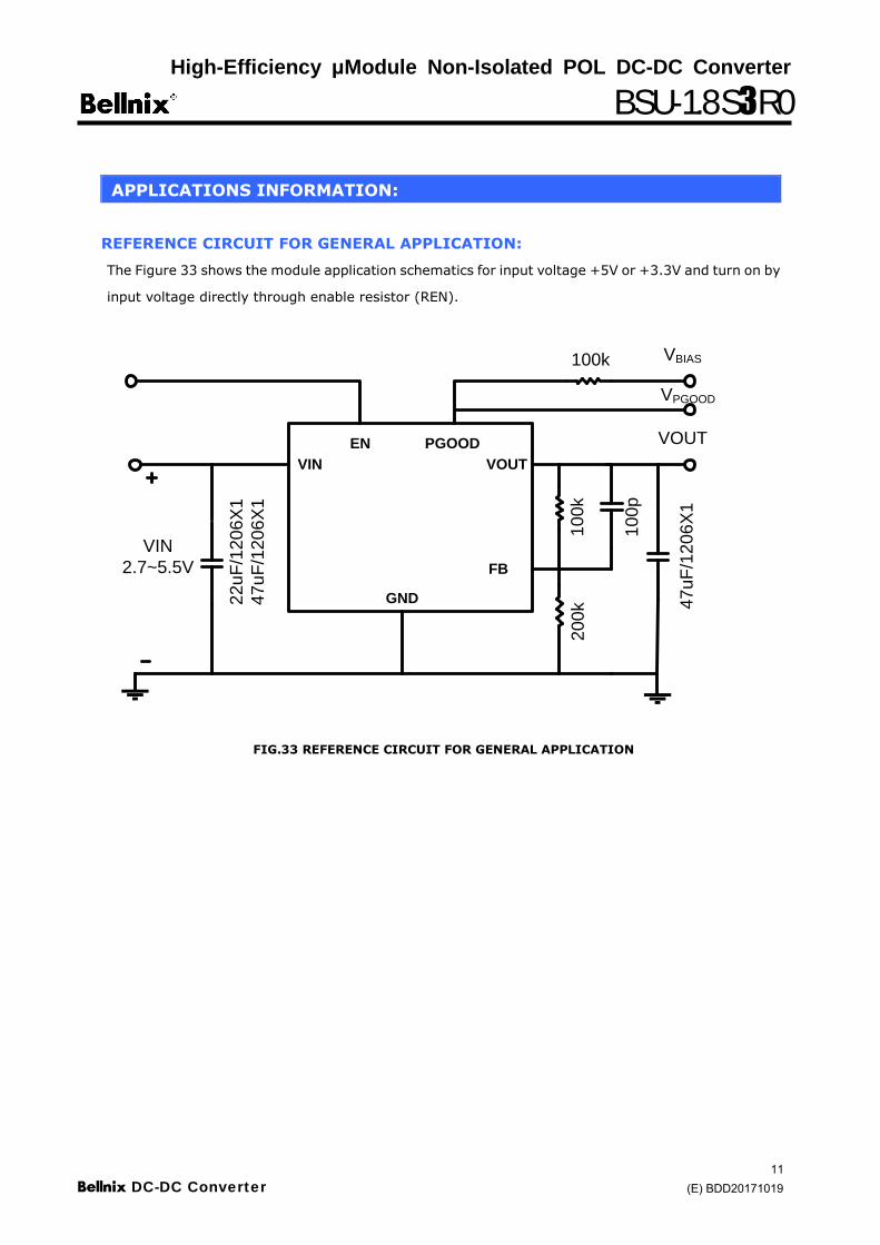
APPLICATIONS INFORMATION:
REFERENCE CIRCUIT FOR GENERAL APPLICATION:
The Figure 33 shows the module application schematics for input voltage +5V or +3.3V and turn on by
input voltage directly through enable resistor (REN).
EN PGOOD
VOUT
FB
GND
VIN
VBIAS
22u
F/1
206
X1
47u
F/1
206
X1
VOUT
VIN
2.7~5.5V100k
200
k
100p
47u
F/1
20
6X
1
100k
VPGOOD
FIG.33 REFERENCE CIRCUIT FOR GENERAL APPLICATION
High-Efficiency μModule Non-Isolated POL DC-DC Converter
BSU-1.8S3R0
Bellnix DC-DC Converter 12
(E) BDD20171019
APPLICATIONS INFORMATION: (Cont.)
SAFETY CONSIDERATIONS:
Certain applications and/or safety agencies may require fuses at the inputs of power conversion
components. Fuses should also be used when there is the possibility of sustained input voltage reversal
which is not current limited. For greatest safety, we recommend a fast blow fuse installed in the
ungrounded input supply line. The installer must observe all relevant safety standards and regulations.
For safety agency approvals, install the converter in compliance with the end-user safety standard.
INPUT FILTERING:
The module should be connected to a low AC impedance source supply and a highly inductive source or
line inductance can affect the stability of the module. An input capacitor must be placed directly to the
input pin of the module, to minimize input ripple voltage and ensure module stability.
OUTPUT FILTERING:
To reduce output ripple and improve the dynamic response to as step load change, the additional
capacitor at the output must be used. Low ESR polymer and ceramic capacitors are recommended to
improve the output ripple and dynamic response of the module.
PROGRAMMING OUTPUT VOLTAGE:
The module has an internal 0.6V±2% reference voltage. The output voltage can be programed by the
dividing resistance RFB which respects to FB pin and GND pin. The output voltage can be calculated as
shown in Equation 1 and the resistor according to typical output voltage is shown in TABLE 1.
1 RFB_bot
RFB_topVOUT (V) 0.6 (EQ.1)
Vout (V) RFB_top (k) RFB_bot (k)
1.0 200(1%) 300(1%)
1.2 200(1%) 200(1%)
1.8 200(1%) 100(1%)
2.5 200(1%) 63.2(1%)
3.3 200(1%) 44.2(1%)
TABLE.01 Resistor values for common output voltages
High-Efficiency μModule Non-Isolated POL DC-DC Converter
BSU-1.8S3R0
Bellnix DC-DC Converter 13
(E) BDD20171019
APPLICATIONS INFORMATION: (Cont.)
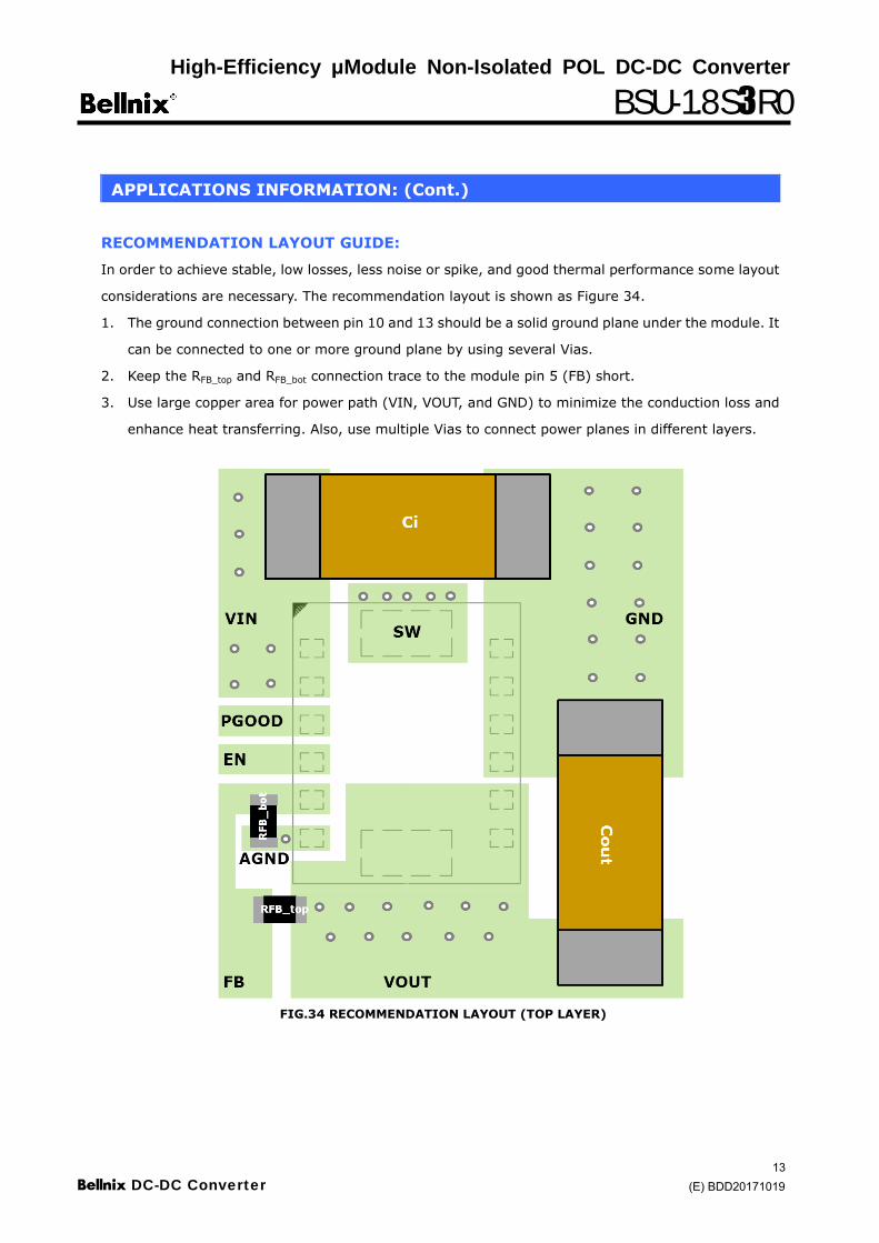
RECOMMENDATION LAYOUT GUIDE:
In order to achieve stable, low losses, less noise or spike, and good thermal performance some layout
considerations are necessary. The recommendation layout is shown as Figure 34.
1. The ground connection between pin 10 and 13 should be a solid ground plane under the module. It
can be connected to one or more ground plane by using several Vias.
2. Keep the RFB_top and RFB_bot connection trace to the module pin 5 (FB) short.
3. Use large copper area for power path (VIN, VOUT, and GND) to minimize the conduction loss and
enhance heat transferring. Also, use multiple Vias to connect power planes in different layers.
FIG.34 RECOMMENDATION LAYOUT (TOP LAYER)
High-Efficiency μModule Non-Isolated POL DC-DC Converter
BSU-1.8S3R0
Bellnix DC-DC Converter 14
(E) BDD20171019
APPLICATIONS INFORMATION: (Cont.)
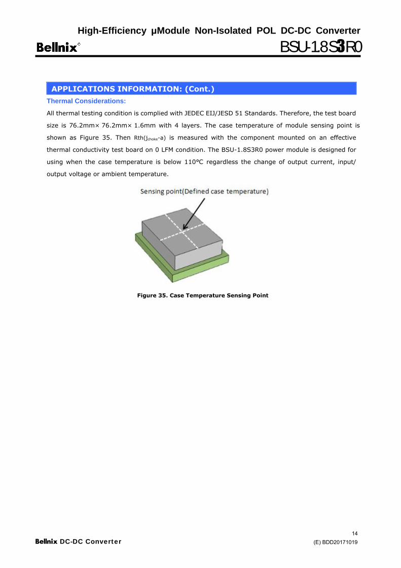
Thermal Considerations:
All thermal testing condition is complied with JEDEC EIJ/JESD 51 Standards. Therefore, the test board
size is 76.2mm× 76.2mm× 1.6mm with 4 layers. The case temperature of module sensing point is
shown as Figure 35. Then Rth(jchoke-a) is measured with the component mounted on an effective
thermal conductivity test board on 0 LFM condition. The BSU-1.8S3R0 power module is designed for
using when the case temperature is below 110°C regardless the change of output current, input/
output voltage or ambient temperature.
Figure 35. Case Temperature Sensing Point
High-Efficiency μModule Non-Isolated POL DC-DC Converter
BSU-1.8S3R0
Bellnix DC-DC Converter 15
(E) BDD20171019
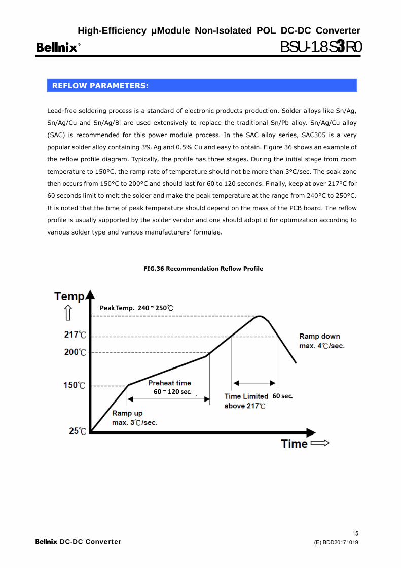
REFLOW PARAMETERS:
Lead-free soldering process is a standard of electronic products production. Solder alloys like Sn/Ag,
Sn/Ag/Cu and Sn/Ag/Bi are used extensively to replace the traditional Sn/Pb alloy. Sn/Ag/Cu alloy
(SAC) is recommended for this power module process. In the SAC alloy series, SAC305 is a very
popular solder alloy containing 3% Ag and 0.5% Cu and easy to obtain. Figure 36 shows an example of
the reflow profile diagram. Typically, the profile has three stages. During the initial stage from room
temperature to 150°C, the ramp rate of temperature should not be more than 3°C/sec. The soak zone
then occurs from 150°C to 200°C and should last for 60 to 120 seconds. Finally, keep at over 217°C for
60 seconds limit to melt the solder and make the peak temperature at the range from 240°C to 250°C.
It is noted that the time of peak temperature should depend on the mass of the PCB board. The reflow
profile is usually supported by the solder vendor and one should adopt it for optimization according to
various solder type and various manufacturers’ formulae.
FIG.36 Recommendation Reflow Profile
℃
High-Efficiency μModule Non-Isolated POL DC-DC Converter
BSU-1.8S3R0
Bellnix DC-DC Converter 16
(E) BDD20171019
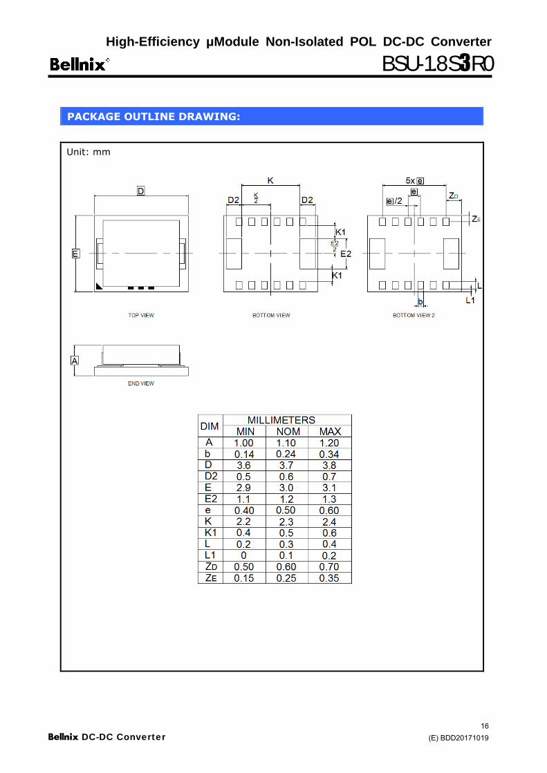
PACKAGE OUTLINE DRAWING:
Unit: mm
High-Efficiency μModule Non-Isolated POL DC-DC Converter
BSU-1.8S3R0
Bellnix DC-DC Converter 17
(E) BDD20171019
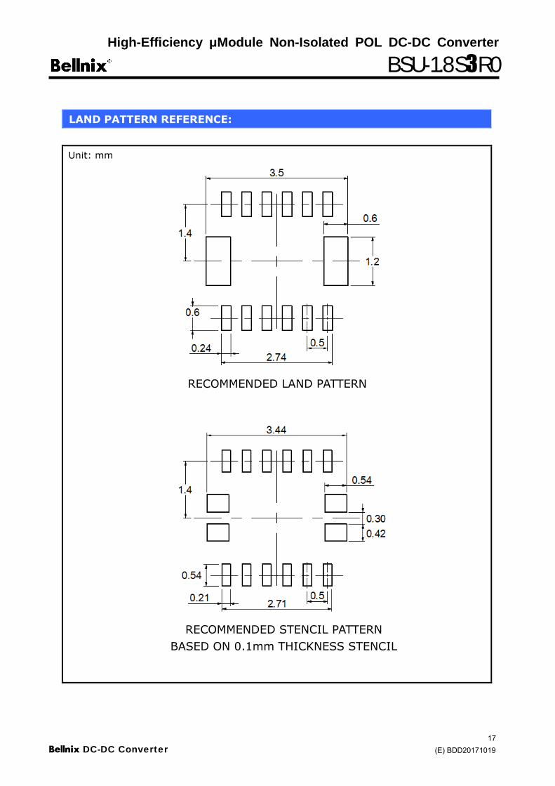
LAND PATTERN REFERENCE:
Unit: mm
RECOMMENDED LAND PATTERN
RECOMMENDED STENCIL PATTERN
BASED ON 0.1mm T HICKNESS STENCIL
High-Efficiency μModule Non-Isolated POL DC-DC Converter
BSU-1.8S3R0
Bellnix DC-DC Converter 18
(E) BDD20171019
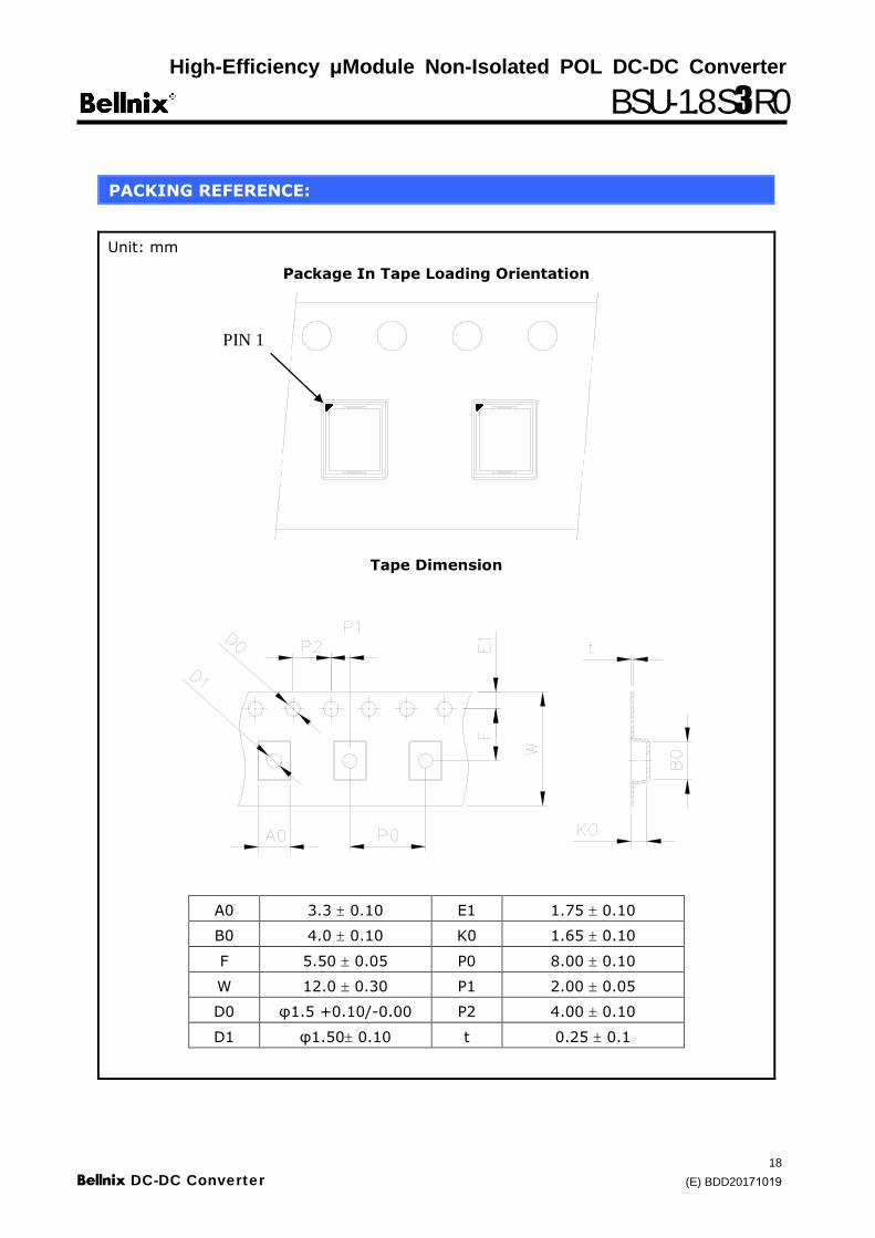
PACKING REFERENCE:
Unit: mm
Package In Tape Loading Orientation
Tape Dimension
A0 3.3 0.10 E1 1.75 0.10
B0 4.0 0.10 K0 1.65 0.10
F 5.50 0.05 P0 8.00 0.10
W 12.0 0.30 P1 2.00 0.05
D0 φ1.5 +0.10/-0.00 P2 4.00 0.10
D1 φ1.50 0.10 t 0.25 0.1
PIN 1
High-Efficiency μModule Non-Isolated POL DC-DC Converter
BSU-1.8S3R0
Bellnix DC-DC Converter 19
(E) BDD20171019
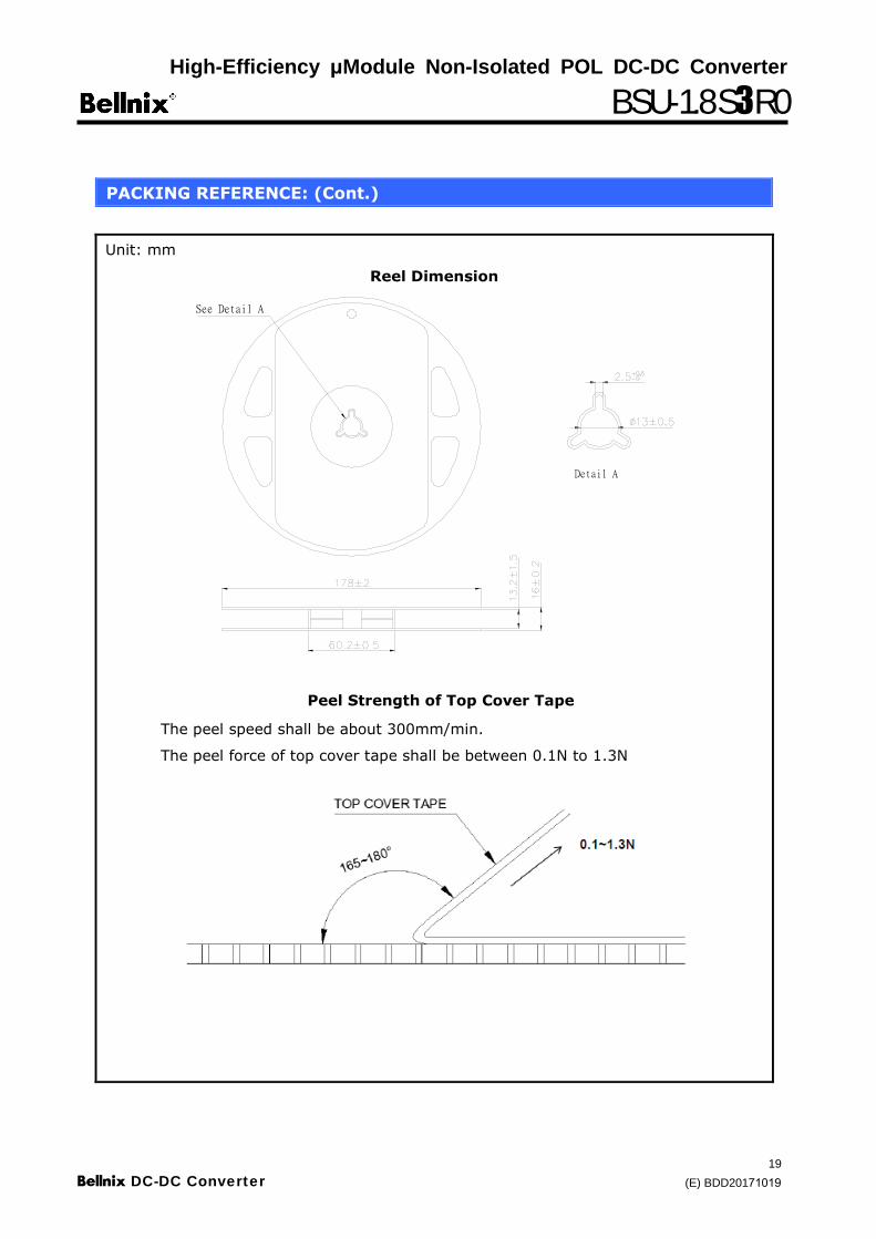
PACKING REFERENCE: (Cont.)
Unit: mm
Reel Dimension
See Detail A
Detail A
Peel Strength of Top Cover Tape
The peel speed shall be about 300mm/min.
The peel force of top cover tape shall be between 0.1N to 1.3N
High-Efficiency μModule Non-Isolated POL DC-DC Converter
BSU-1.8S3R0■ Precautions for use
To ensure user’s safety, check specifications before using the product and always observe the followingprecautions for use.・ This product is intended for use in general electronics equipment (office equipment, communication
equipment, measurement equipment). Do not use the product for medical equipment, nuclear equipment, trains, etc., whereby human life or property may be directly affected by damaged product. Consult with us for any use other than for such general electronics equipment.
・ This product is not suitable for serial or parallel operation. ・ Do not use connectors and sockets for mounting the product. Contact resistance may have an
adverse effect on the performance. Use the soldering method for mounting on the printed circuit board.
・ This equipment has a built-in over current protection circuit but avoid a prolonged short circuit which may lead to failure.
・ This product may be damaged if used under nonstandard electrical conditions or nonstandard environmental conditions including temperature. Ensure use within the standards.
・ Avoid using this product in a place that generates corrosive gas or is dusty. ・ This product may be damaged by static electricity. Make sure that the workplace is guarded against
static buildup and static electricity on operators by use of proper grounding. ・ A fuse mechanism is not built in this product. Connect a fuse to +input line to guard against
excessive input current under abnormal circumstances. Allow enough capacity for power supply for a fuse to blow.
・ This product has no build-in function for over voltage protection. If over voltage occurs due to anomalies in the module, input voltage is output, as is, in the same mode, which may result in fumes and ignition. To prevent this from occurring, always add an over voltage protection circuit.
・ This product does not come with a test report.
■ WarrantyThe warranty term of the product is one year after shipment. Should the product become defectivewithin the warranty period due to our design or workmanship, the product will be repaired free of chargeor replaced.However, this warranty does not cover products which have been subjected to unauthorized innermodifications, etc.
The scope of our warranty is limited to that of the said product.
■ Miscellaneous mattersAny doubt arising out of or in connection with these specifications shall be determined upon mutualconsultation between the parties concerned.
■ ContactIf you have any further technical questions for this product, please contact us.E-mail: [email protected]: http://www.bellnix.com
Bellnix DC-DC Converter 20
(E) BDD20171019