Embed Size (px)
Citation preview

High Efficiency solidHigh Efficiency solidstate amplifiersstate amplifiers
EME Conference 2010, Dallas TexasGoran Popovic AD6IW
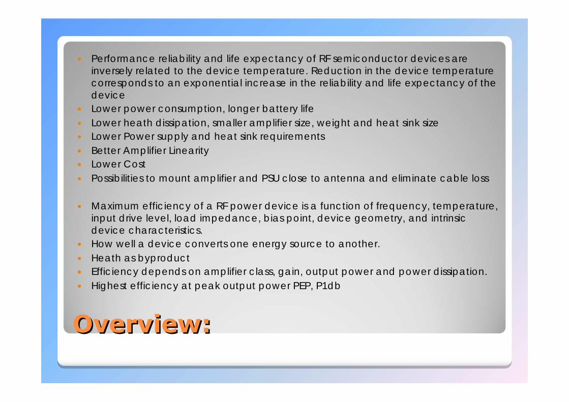
Overview:Overview:
Performance reliability and life expectancy of RF semiconductor devices areinversely related to the device temperature. Reduction in the device temperaturecorresponds to an exponential increase in the reliability and life expectancy of thedevice
Lower power consumption, longer battery life Lower heath dissipation, smaller amplifier size, weight and heat sink size Lower Power supply and heat sink requirements Better Amplifier Linearity Lower Cost Possibilities to mount amplifier and PSU close to antenna and eliminate cable loss
Maximum efficiency of a RF power device is a function of frequency, temperature,input drive level, load impedance, bias point, device geometry, and intrinsicdevice characteristics.
How well a device converts one energy source to another. Heath as byproduct Efficiency depends on amplifier class, gain, output power and power dissipation. Highest efficiency at peak output power PEP, P1db

Drain Efficiency and PAEDrain Efficiency and PAE
Drain efficiency
Power added efficiency, PAE

Drain Efficiency and PAE vs. VdsDrain Efficiency and PAE vs. Vds
Drain Efficiency and PAE as a function of Vds for a classB LDMOS power amplifier
Average efficiency ηAVG = PoutAVG/PinAVG
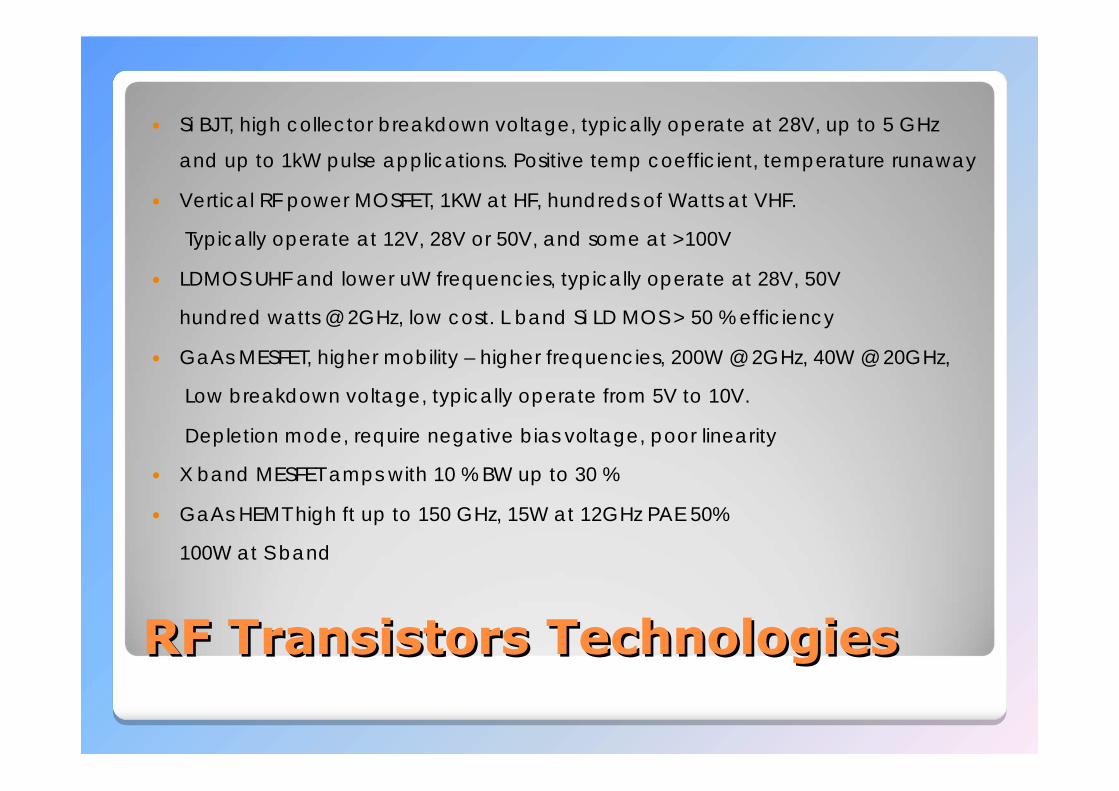
RF Transistors TechnologiesRF Transistors Technologies
Si BJT, high collector breakdown voltage, typically operate at 28V, up to 5 GHz
and up to 1kW pulse applications. Positive temp coefficient, temperature runaway
Vertical RF power MOSFET, 1KW at HF, hundreds of Watts at VHF.
Typically operate at 12V, 28V or 50V, and some at >100V
LDMOS UHF and lower uW frequencies, typically operate at 28V, 50V
hundred watts @ 2GHz, low cost. L band Si LD MOS > 50 % efficiency
GaAs MESFET, higher mobility – higher frequencies, 200W @ 2GHz, 40W @ 20GHz,
Low breakdown voltage, typically operate from 5V to 10V.
Depletion mode, require negative bias voltage, poor linearity
X band MESFET amps with 10 % BW up to 30 %
GaAs HEMT high ft up to 150 GHz, 15W at 12GHz PAE 50%
100W at S band
RF Transistors TechnologiesRF Transistors Technologies
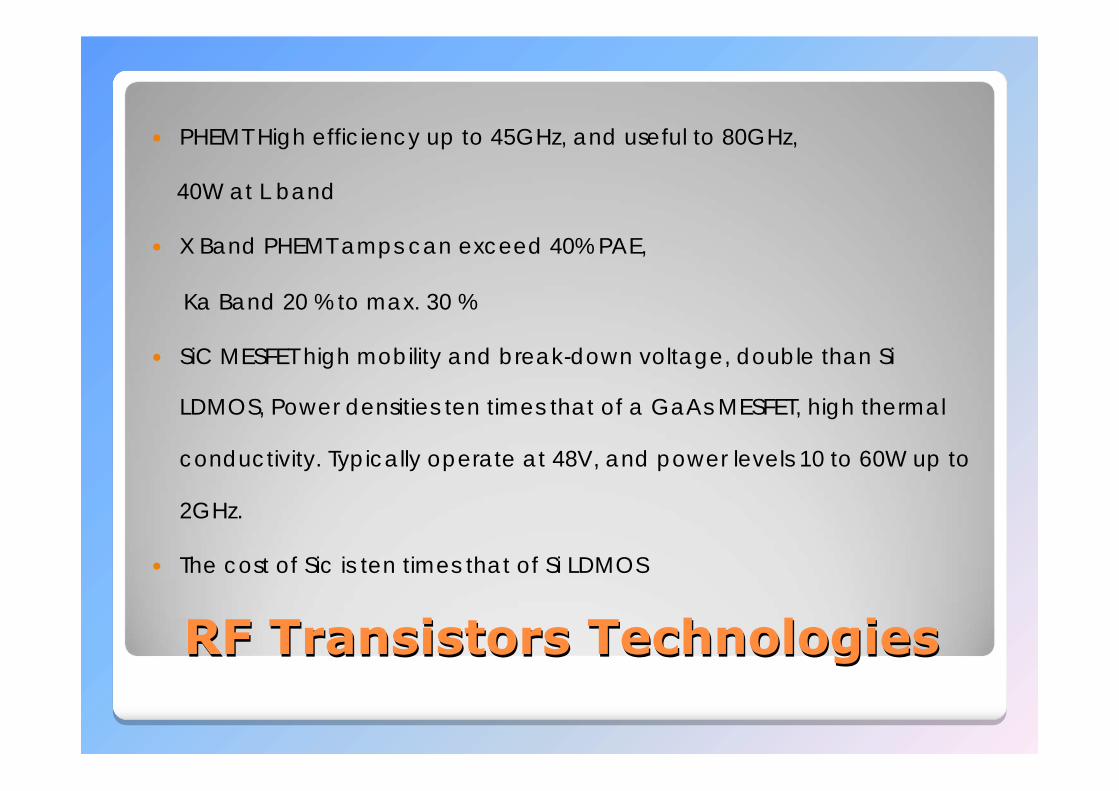
PHEMT High efficiency up to 45GHz, and useful to 80GHz,
40W at L band
X Band PHEMT amps can exceed 40% PAE,
Ka Band 20 % to max. 30 %
SiC MESFET high mobility and break-down voltage, double than Si
LDMOS, Power densities ten times that of a GaAs MESFET, high thermal
conductivity. Typically operate at 48V, and power levels 10 to 60W up to
2GHz.
The cost of Sic is ten times that of Si LDMOS
RF Transistors TechnologiesRF Transistors Technologies
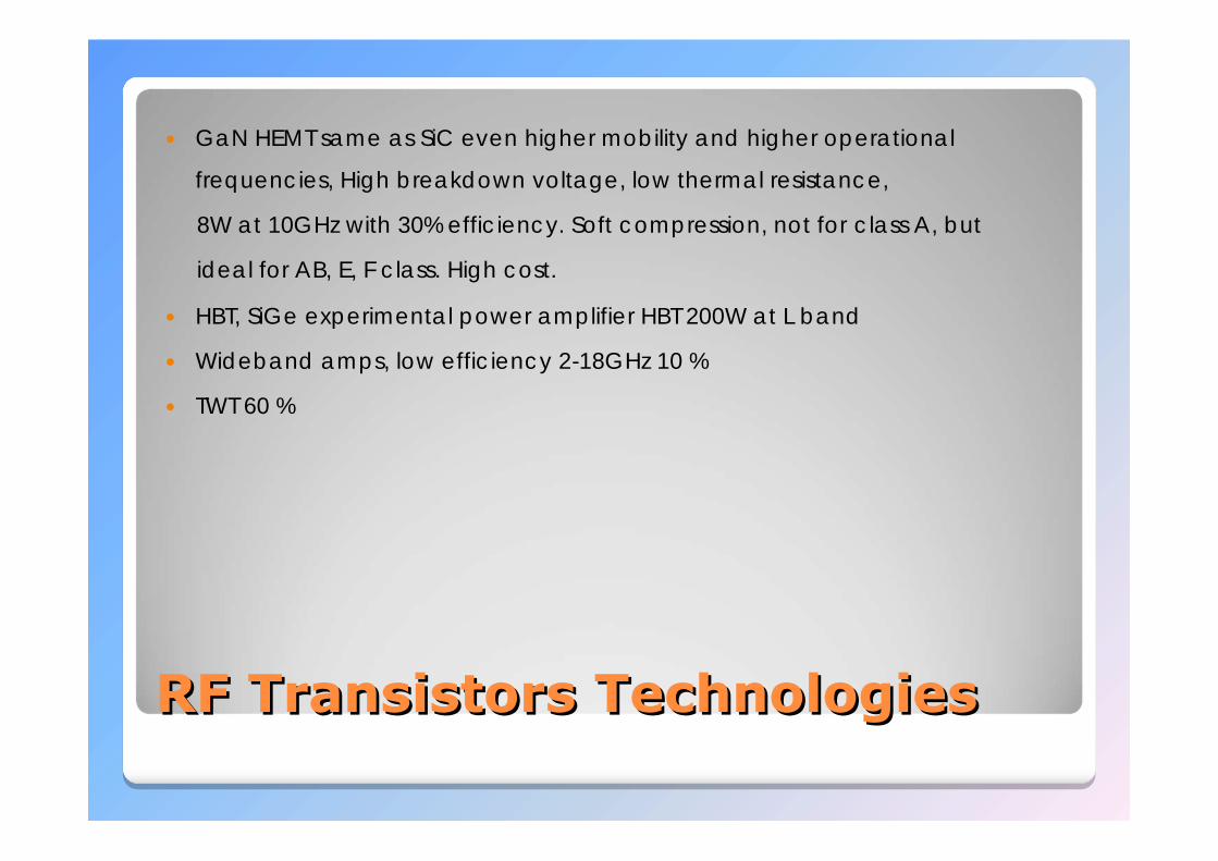
GaN HEMT same as SiC even higher mobility and higher operational
frequencies, High breakdown voltage, low thermal resistance,
8W at 10GHz with 30% efficiency. Soft compression, not for class A, but
ideal for AB, E, F class. High cost.
HBT, SiGe experimental power amplifier HBT 200W at L band
Wideband amps, low efficiency 2-18GHz 10 %
TWT 60 %
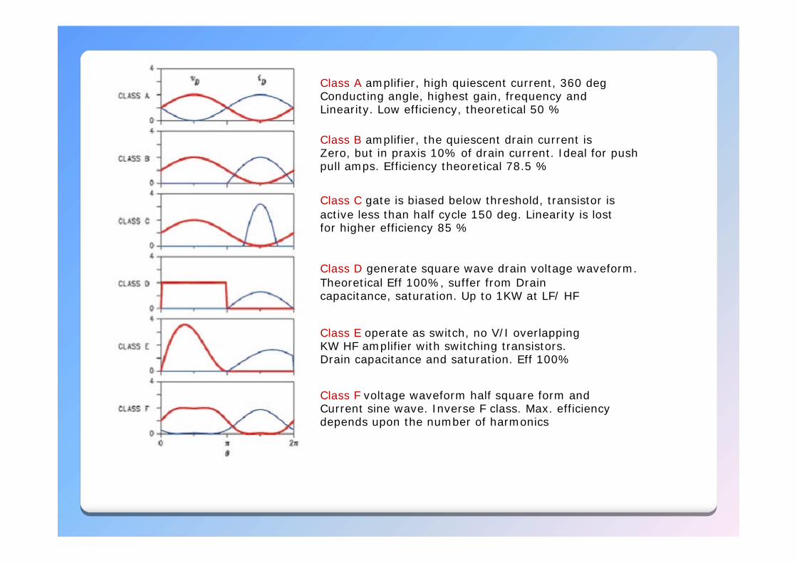
Class A amplifier, high quiescent current, 360 degConducting angle, highest gain, frequency andLinearity. Low efficiency, theoretical 50 %
Class B amplifier, the quiescent drain current isZero, but in praxis 10% of drain current. Ideal for pushpull amps. Efficiency theoretical 78.5 %
Class C gate is biased below threshold, transistor isactive less than half cycle 150 deg. Linearity is lostfor higher efficiency 85 %
Class D generate square wave drain voltage waveform.Theoretical Eff 100%, suffer from Draincapacitance, saturation. Up to 1KW at LF/ HF
Class E operate as switch, no V/I overlappingKW HF amplifier with switching transistors.Drain capacitance and saturation. Eff 100%
Class F voltage waveform half square form andCurrent sine wave. Inverse F class. Max. efficiencydepends upon the number of harmonics
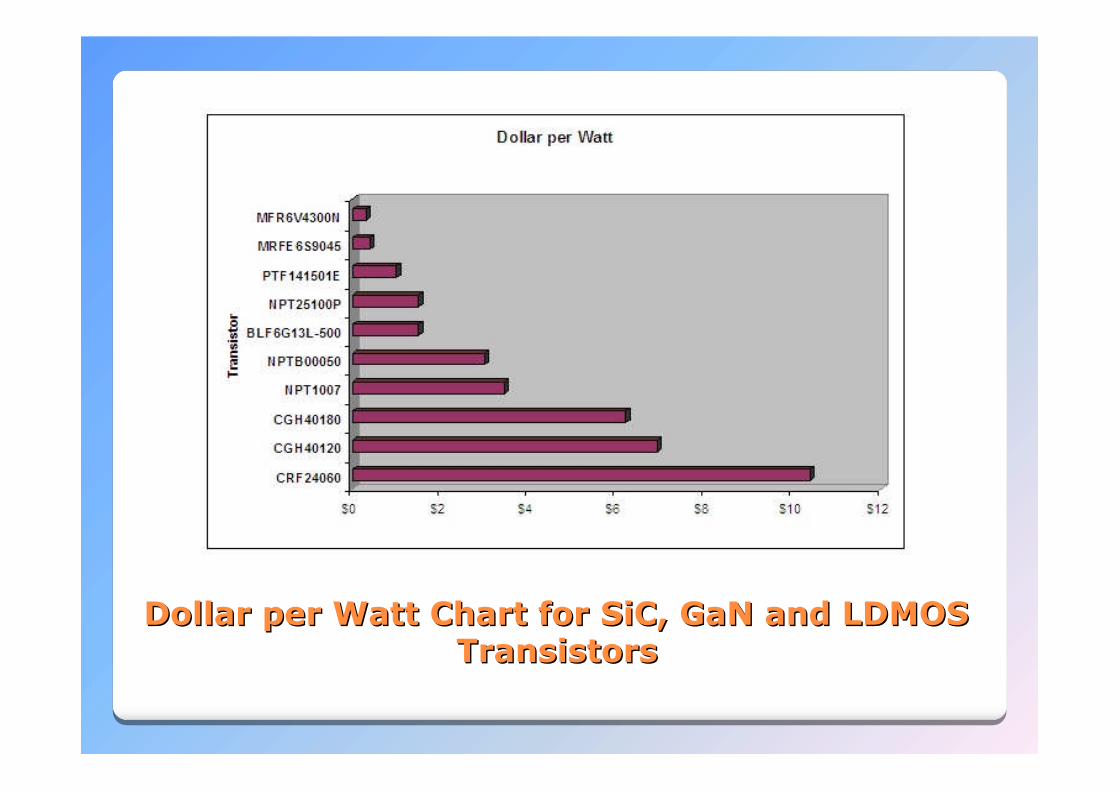
Dollar per Watt Chart for SiC, GaN and LDMOSDollar per Watt Chart for SiC, GaN and LDMOSTransistorsTransistors
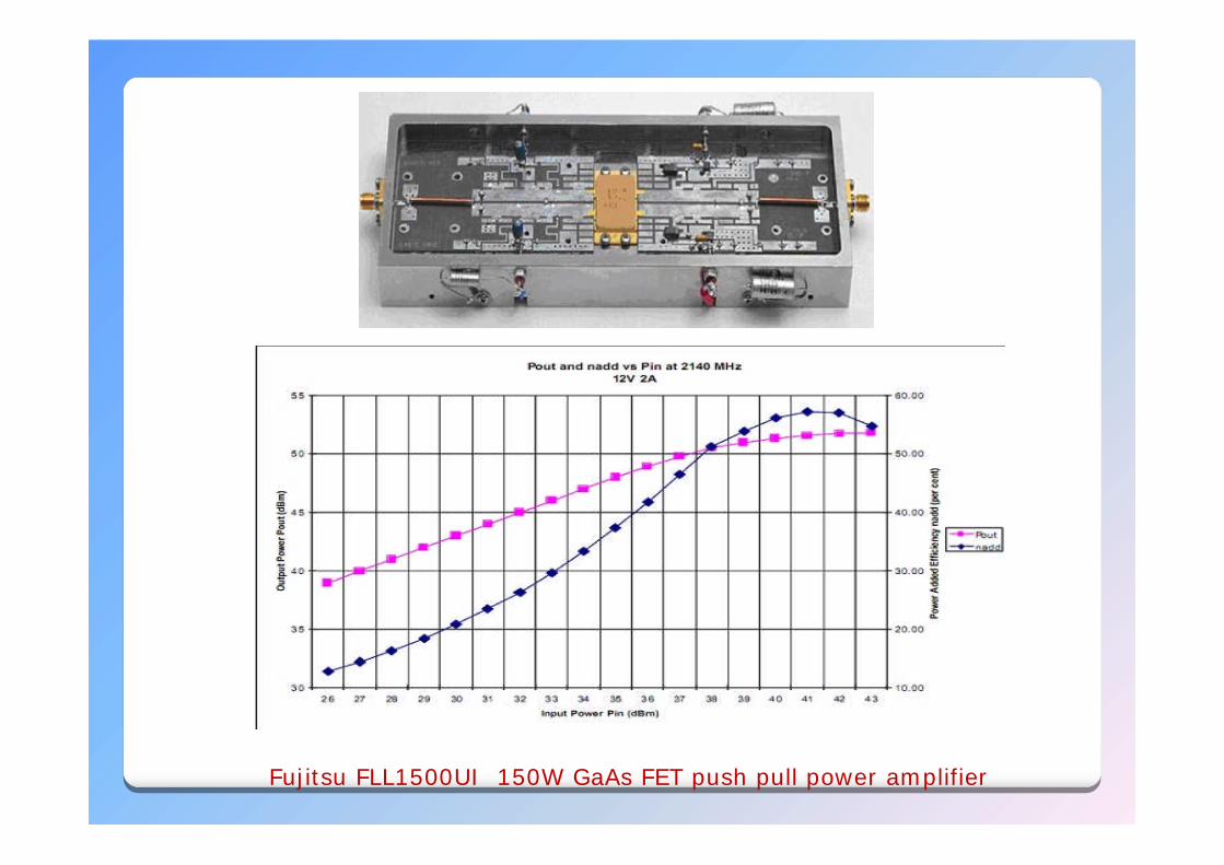
Fujitsu FLL1500UI 150W GaAs FET push pull power amplifier
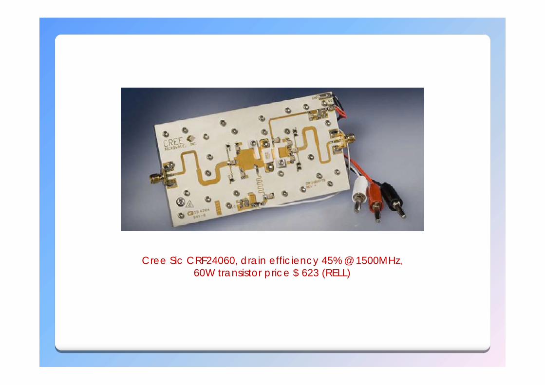
Cree Sic CRF24060, drain efficiency 45% @ 1500MHz,60W transistor price $ 623 (RELL)
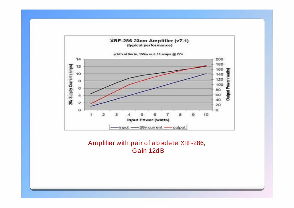
Amplifier with pair of absolete XRF-286,Gain 12dB
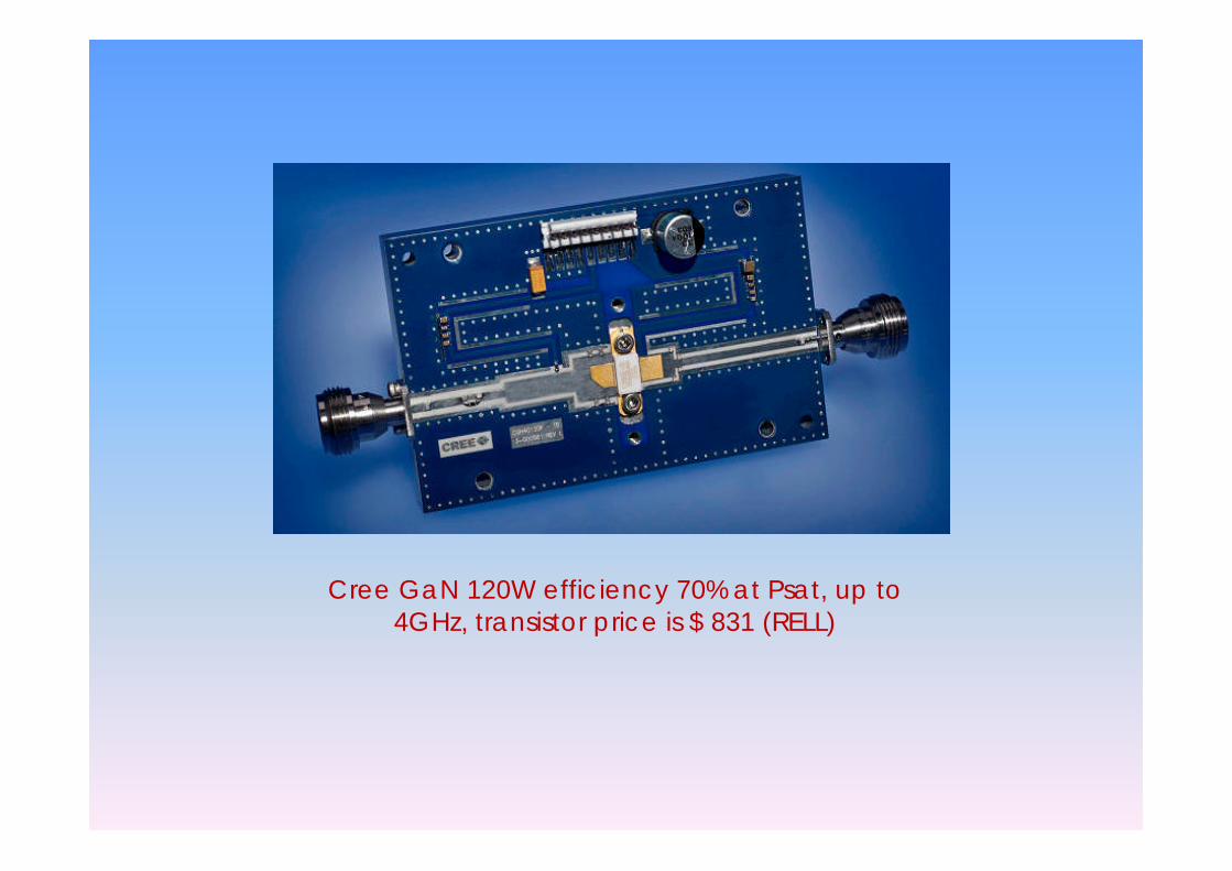
Cree GaN 120W efficiency 70% at Psat, up to4GHz, transistor price is $ 831 (RELL)

Infineon PTF141501E 150W Efficiency 48%,Transistor price is $154 (RELL)
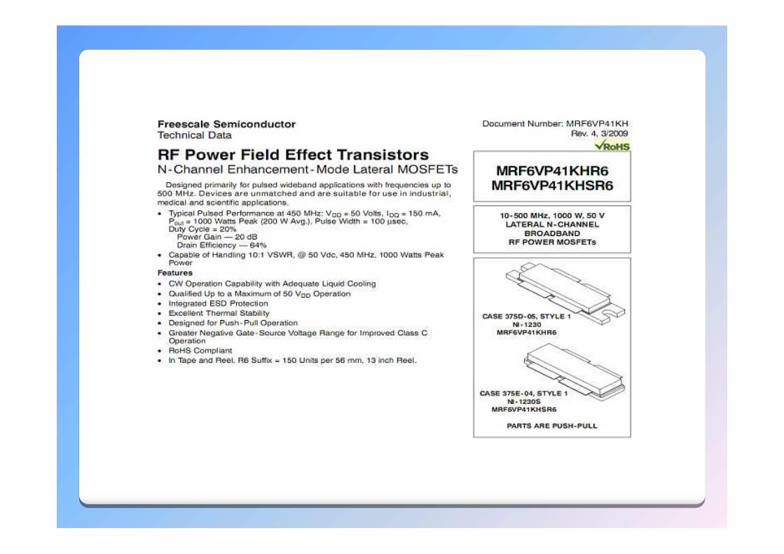
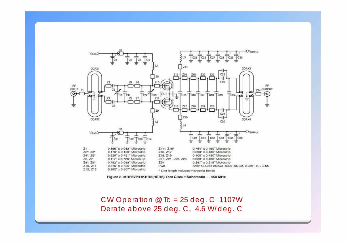
CW Operation @ Tc = 25 deg. C 1107WDerate above 25 deg. C, 4.6 W/deg. C
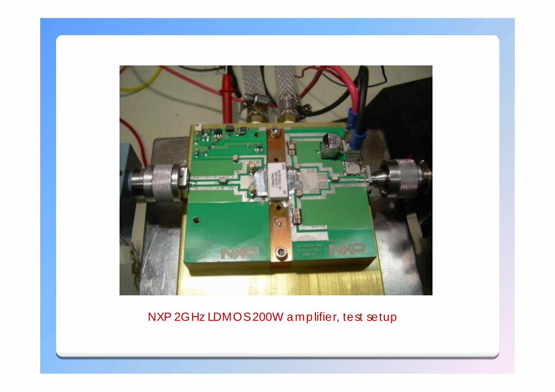
NXP 2GHz LDMOS 200W amplifier, test setup
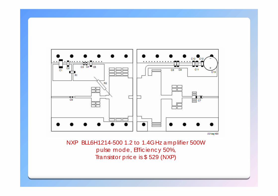
NXP BLL6H1214-500 1.2 to 1.4GHz amplifier 500Wpulse mode, Efficiency 50%,Transistor price is $ 529 (NXP)
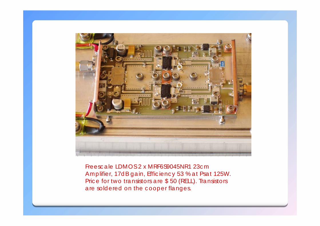
Freescale LDMOS 2 x MRF6S9045NR1 23cmAmplifier, 17dB gain, Efficiency 53 % at Psat 125W.Price for two transistors are $ 50 (RELL). Transistorsare soldered on the cooper flanges.
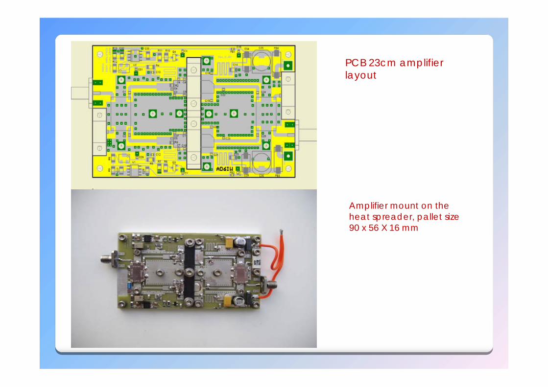
PCB 23cm amplifierlayout
Amplifier mount on theheat spreader, pallet size90 x 56 X 16 mm
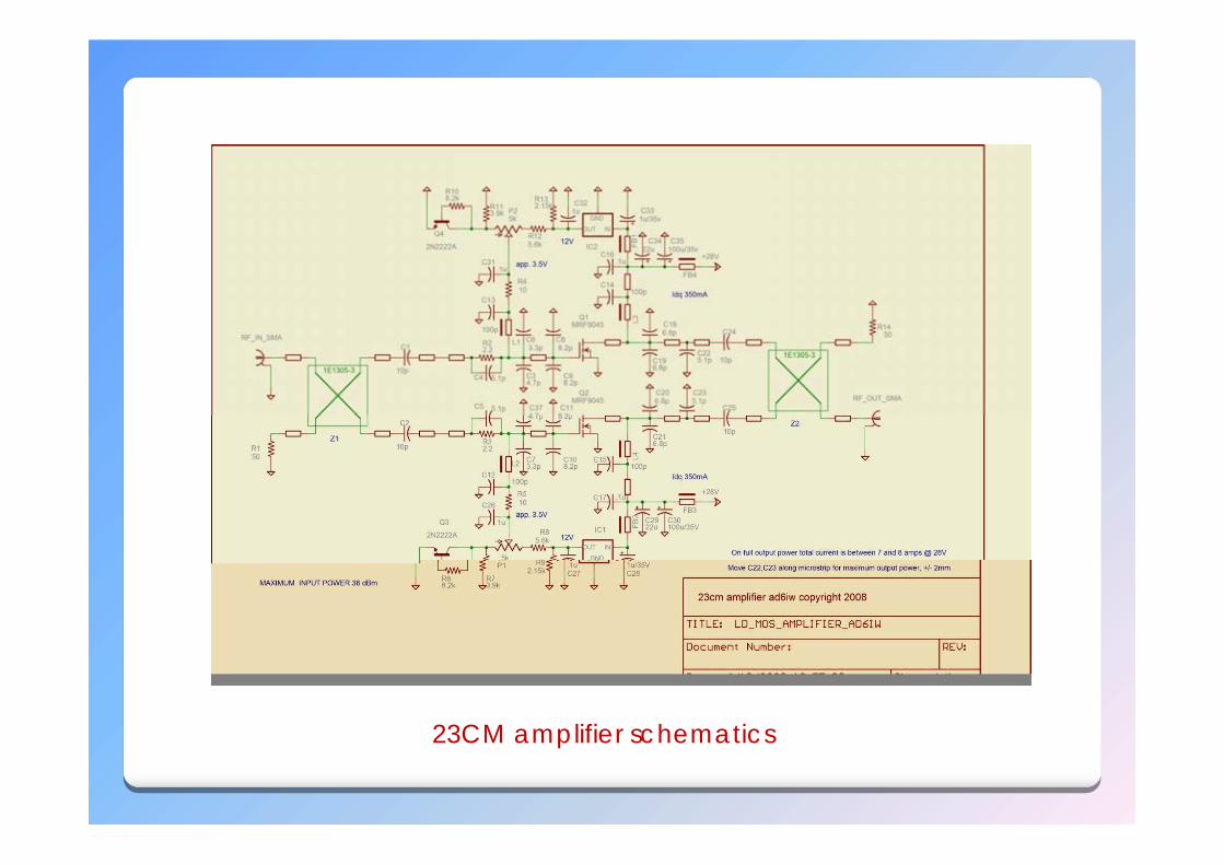
23CM amplifier schematics
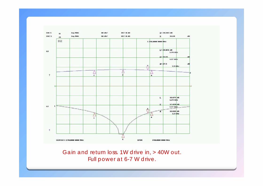
Gain and return loss. 1W drive in, > 40W out.Full power at 6-7 W drive.
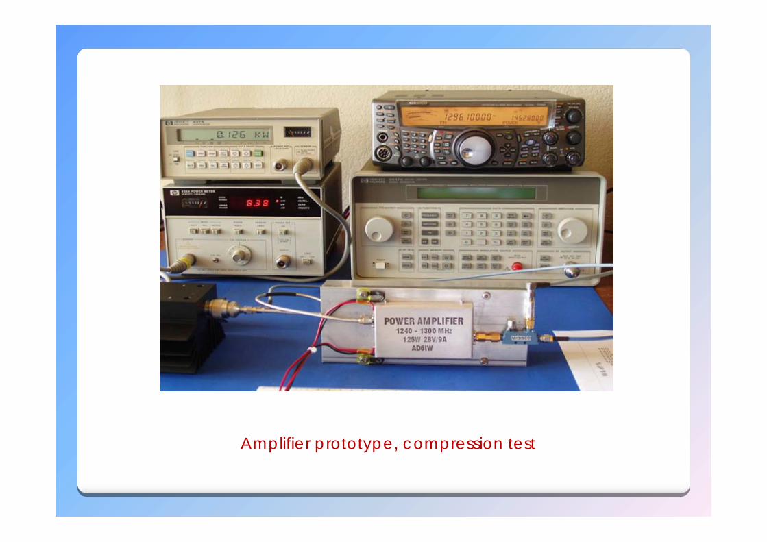
Amplifier prototype, compression test
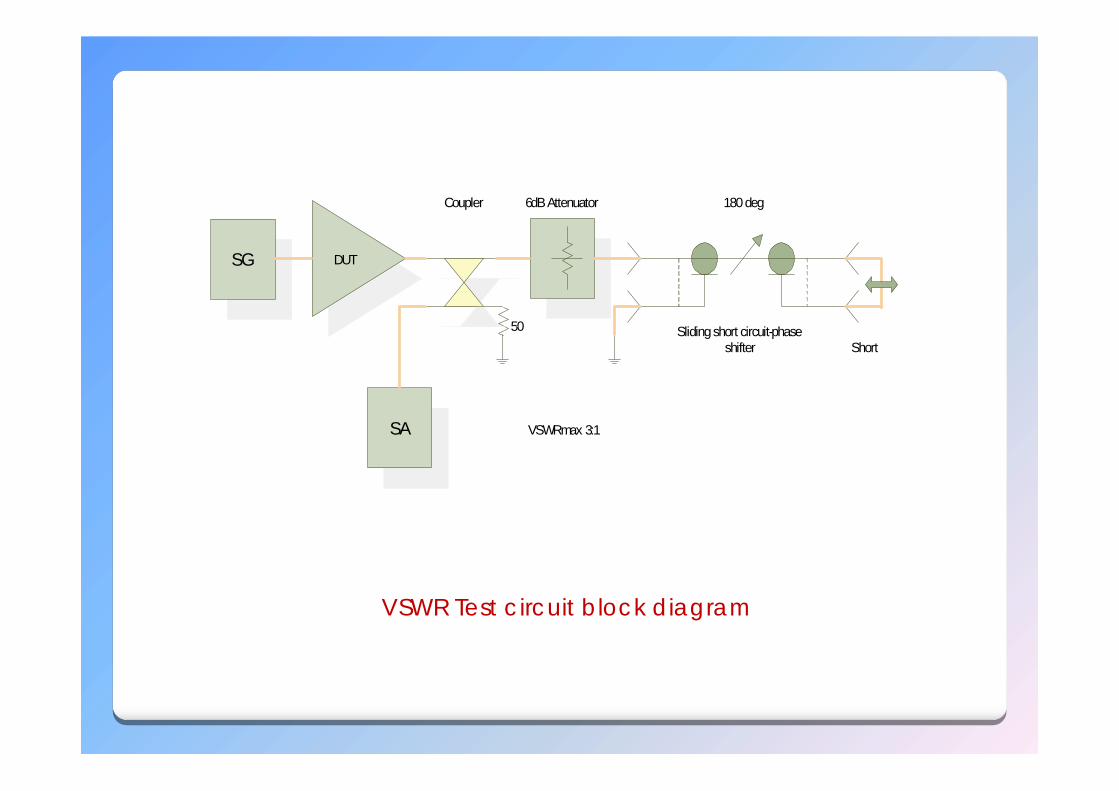
VSWR Test circuit block diagram
SG
SA
50
DUT
6dBAttenuator
VSWRmax 3:1
180deg
ShortSlidingshort circuit-phase
shifter
Coupler

Ready made125W 23cm amplifiers, scaled to MitsubishiRA18H1213G 18W power module.Efficiency of Mitsubishi RF MOSFET module is 28 % atPsat, and 20 % at 18W output power.
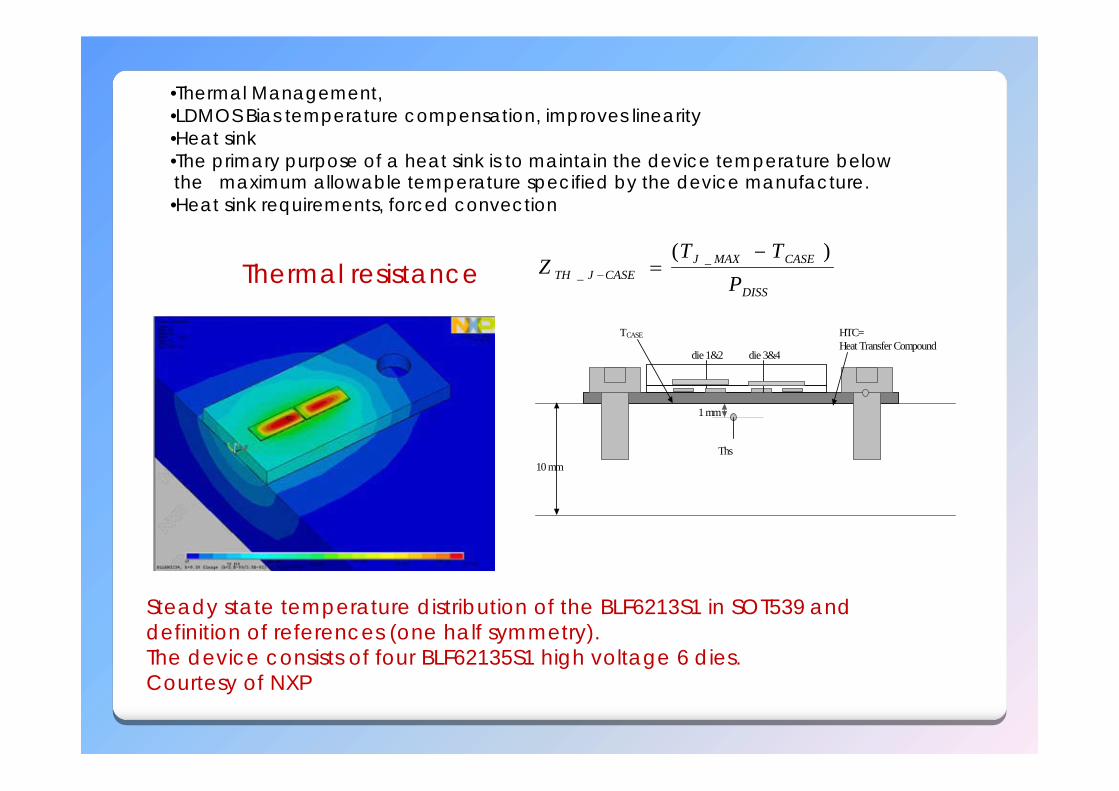
Steady state temperature distribution of the BLF6213S1 in SOT539 anddefinition of references (one half symmetry).The device consists of four BLF62135S1 high voltage 6 dies.Courtesy of NXP
die 3&4die 1&2
Ths10 mm
1 mm
HTC=Heat Transfer Compound
TCASE
•Thermal Management,•LDMOS Bias temperature compensation, improves linearity•Heat sink•The primary purpose of a heat sink is to maintain the device temperature belowthe maximum allowable temperature specified by the device manufacture.•Heat sink requirements, forced convection
DISS
CASEMAXJCASEJTH P
TTZ
)( __
Thermal resistance
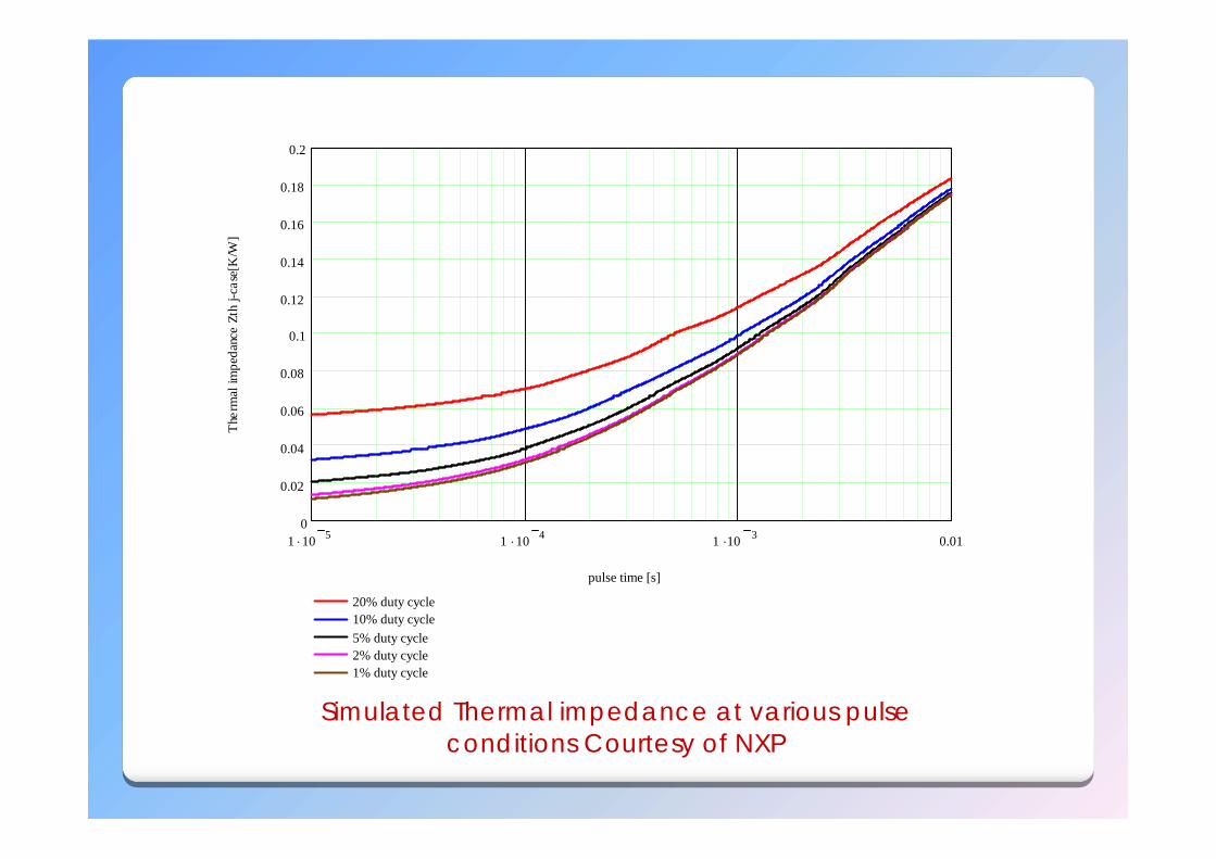
Simulated Thermal impedance at various pulseconditions Courtesy of NXP
1 10 5 1 10 4 1 10 3 0.010
0.02
0.04
0.06
0.08
0.1
0.12
0.14
0.16
0.18
0.2
20% duty cycle10% duty cycle5% duty cycle2% duty cycle1% duty cycle
pulse time [s]
The
rmal
impe
danc
eZt
hj-c
ase[
K/W
]
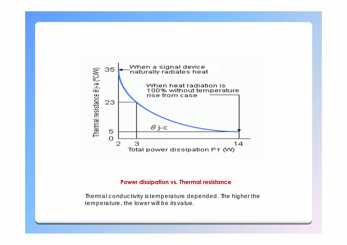
Power dissipation vs. Thermal resistance
Thermal conductivity is temperature depended. The higher thetemperature, the lower will be its value.
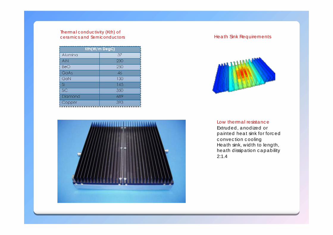
Heath Sink RequirementsThermal conductivity (Kth) ofceramics and Semiconductors
Low thermal resistanceExtruded, anodized orpainted heat sink for forcedconvection coolingHeath sink, width to length,heath dissipation capability2:1.4
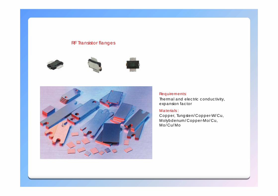
Requirements:Thermal and electric conductivity,expansion factor
Materials :Copper, Tungsten/Copper-W/Cu,Molybdenum/Copper-Mo/Cu,Mo/Cu/Mo
RF Transistor flanges
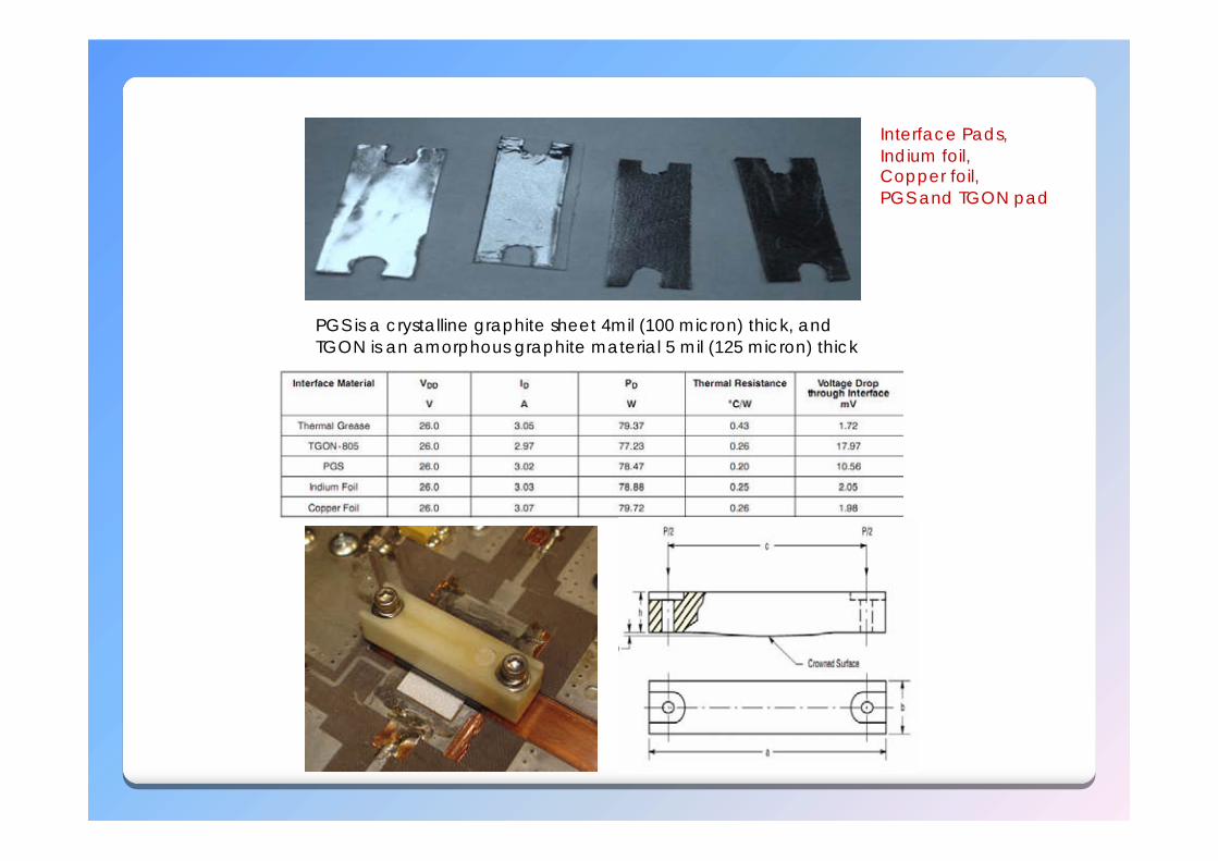
Interface Pads,Indium foil,Copper foil,PGS and TGON pad
PGS is a crystalline graphite sheet 4mil (100 micron) thick, andTGON is an amorphous graphite material 5 mil (125 micron) thick
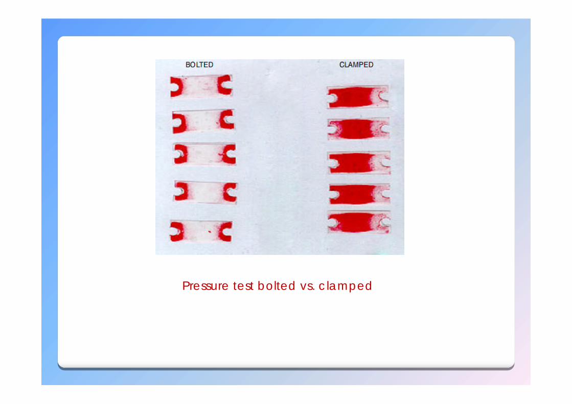
Pressure test bolted vs. clamped
180deg
180deg
AMP A
AMP B
RF_OUT
RF_INP
90 deg 90 deg
AMP A
AMP B
AMP A
AMP B
RF_OUT
RF_INP
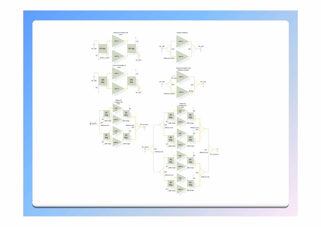
Balanced Amplifier ABclass
Push Pull Amplifier Bclass
Parallel amplifiers
RF_OUTRF_INP
Branch coupler Wilkinson Divider
AMP A
AMP B
Balanced amplifier withWilkinson dividers
RF_OUTRF_INP
Wilkinson Divider
90 deg
90 deg
100 100
100 100
50
50
50
50
90deg
90deg
AMPA
AMP B
BalancedAmplifier AB
class
3dB Xinger
50
50
90deg
90deg
AMPA
AMP B3dB Xinger
50
50
90deg
90deg
AMPA
AMP B3dB Xinger
50
50
90deg
90deg
AMPA
AMP B3dB Xinger
50
50
RF_INPUT
RF_OUTPUT
3dB Xinger
3dB Xinger
3dB Xinger
3dB Xinger100
100
100
Wilkinson div.
100
100
100
Wilkinson div.
Wilkinson div.
Wilkinson div.
Wilkinson div.
Wilkinson div.
90deg
90deg
AMPA
AMP B
BalancedAmplifier AB
class
3dB Xinger
50
50
90deg
90deg
AMPA
AMP B3dB Xinger
50
503dB Xinger
3dB Xinger100
100Wilkinson div. Wilkinson div.
RF_INPUT RF_OUTPUT
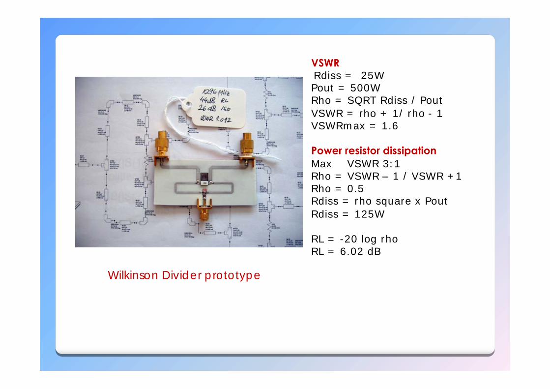
Wilkinson Divider prototype
VSWRRdiss = 25WPout = 500WRho = SQRT Rdiss / PoutVSWR = rho + 1/ rho - 1VSWRmax = 1.6
Power resistor dissipationMax VSWR 3:1Rho = VSWR – 1 / VSWR +1Rho = 0.5Rdiss = rho square x PoutRdiss = 125W
RL = -20 log rhoRL = 6.02 dB
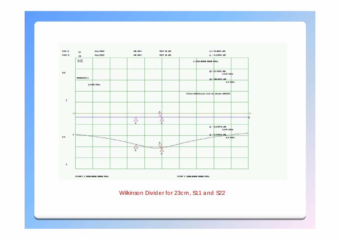
Wilkinson Divider for 23cm, S11 and S22
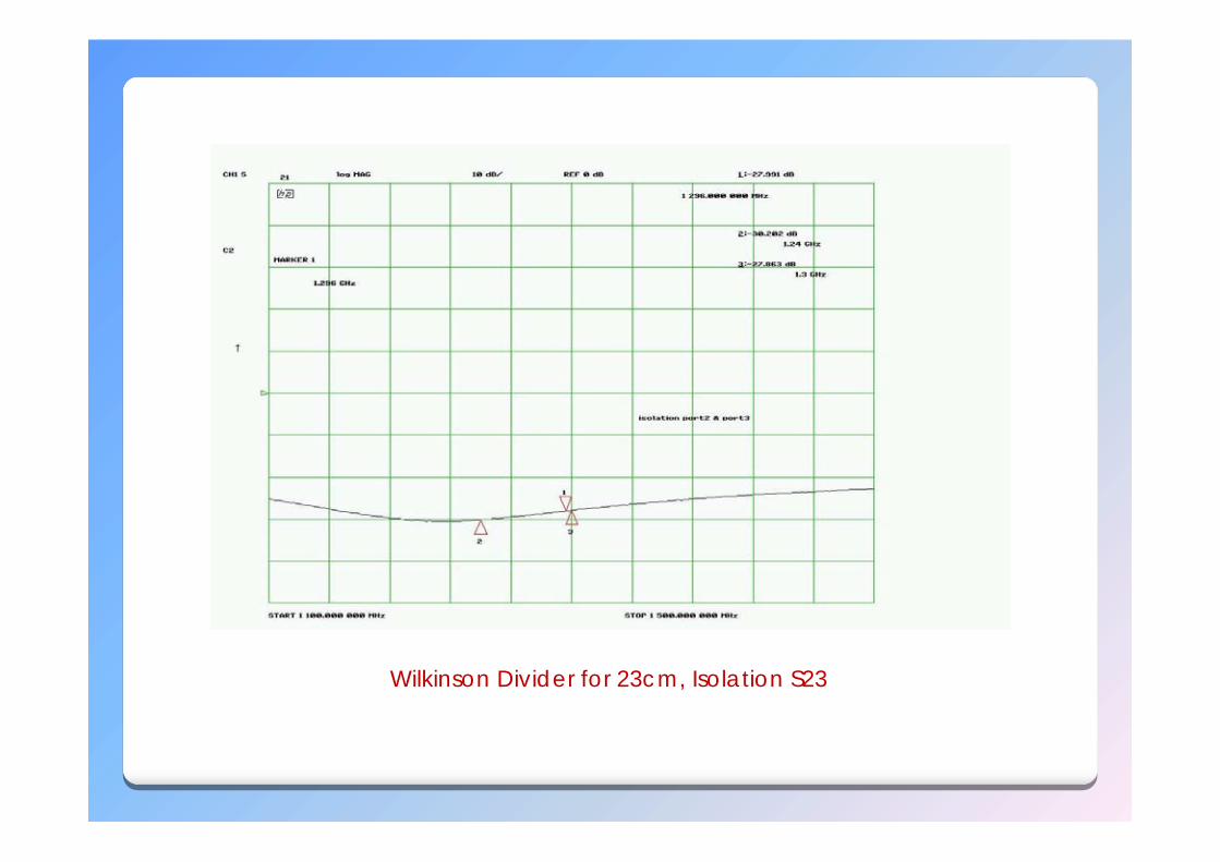
Wilkinson Divider for 23cm, Isolation S23
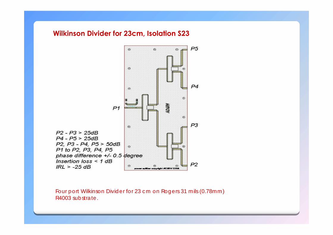
Four port Wilkinson Divider for 23 cm on Rogers 31 mils (0.78mm)R4003 substrate.
Wilkinson Divider for 23cm, Isolation S23
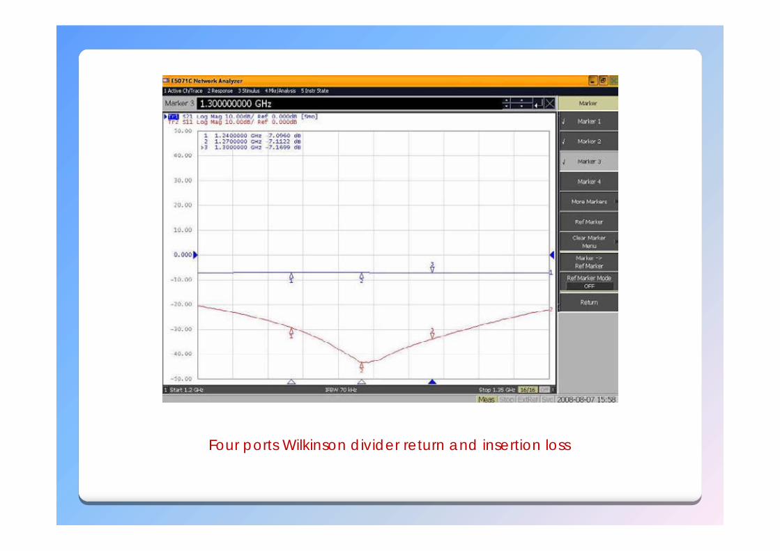
Four ports Wilkinson divider return and insertion loss
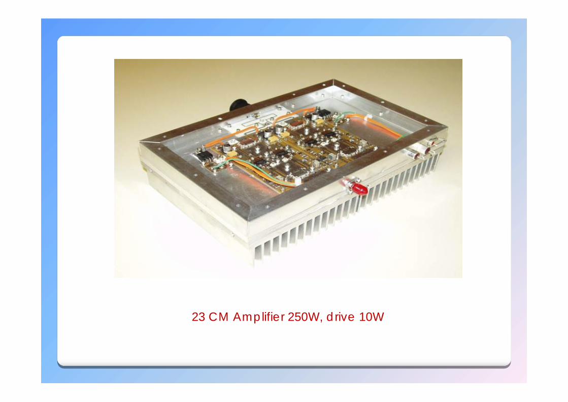
23 CM Amplifier 250W, drive 10W
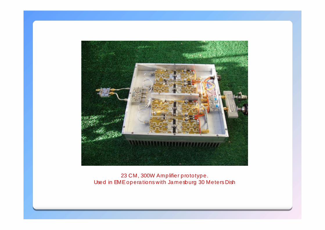
23 CM, 300W Amplifier prototype.Used in EME operations with Jamesburg 30 Meters Dish
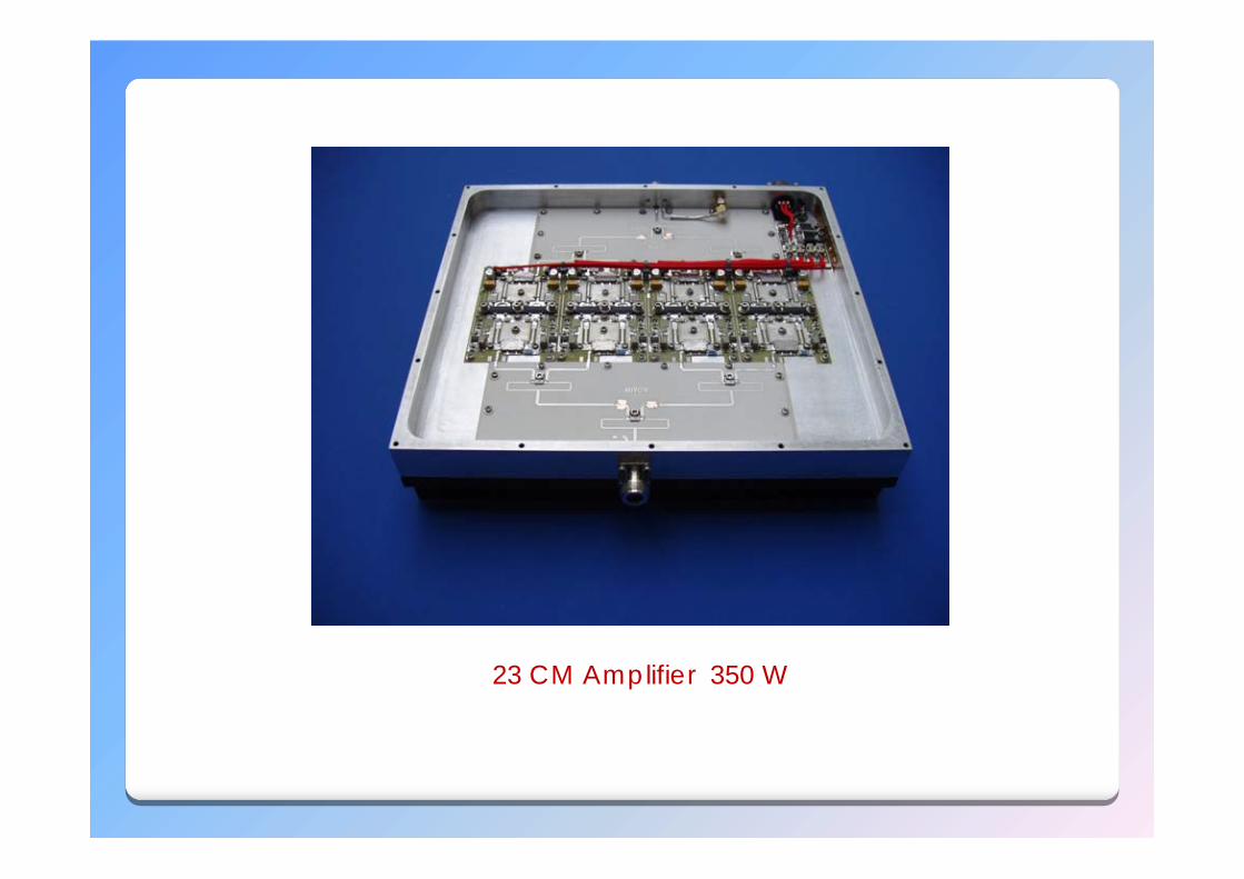
23 CM Amplifier 350 W
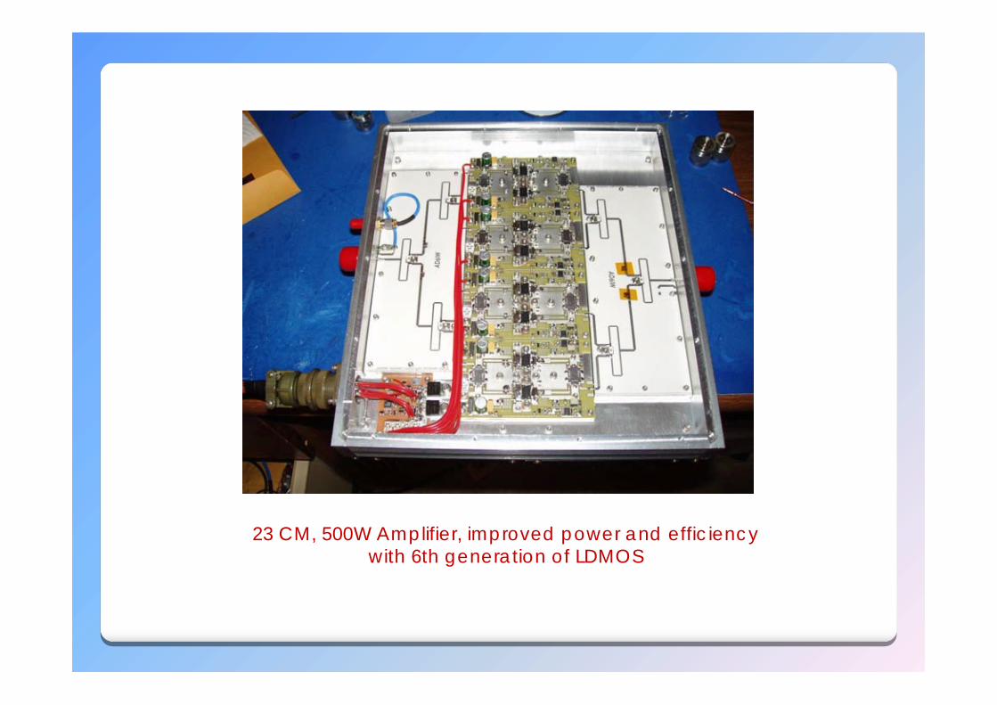
23 CM, 500W Amplifier, improved power and efficiencywith 6th generation of LDMOS
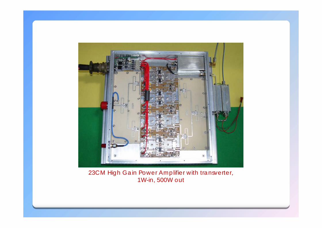
23CM High Gain Power Amplifier with transverter,1W-in, 500W out
ReferencesReferences
Maresh Shah, Richard Rowan, Lu Li Quan Li, Eddie Mares, and Leonard Pelletier AN3789 Clamping of high power RF transistors and RFIC in Over-Molded plastic Packages
Andreas Adahl, Herbert Zirath, An 1GHz Class E LDMOS Power Amplifier Andrei Grebennikov, Power Combiners, Impedance Transformers and Directional Couplers Antonio Equizabal, High Frequency Design, A 300W Power Amplifier for the 88 to 108 MHz FM broadcast Band Frederick H. Raab, Peter Asbeck, Steve Cripps, Peter B. Kenington, Zoya B. Popovic, Nick Pothecary, John F. Sevic and Nathan O. Sokal. High
Frequency Design, RF and Microwave Power Amplifier and Transmitter Technologies part 1 to 4 Alberto Asensio, José Luis Serrano, Javier Gismero and Alvaro Blanco Universidad Politécnica de Madrid, Department of Signals Systems and
Radiocommunications, LDMOS Technolgy Solid-State Transmitter for MIDS Communications System UCSB diploma Thesis byThomas Dellsperger, Device Evaluation for Current-Mode Class-D RF Power Amplifiers Wlodzimierz Janke, Jaroslaw Krasniewski, ISSN 0860-8229 M&M Investigation of Transient Themal Characteristcs of Microwave Transistors J.H.Harris, R.Enck, N. Leonardi, E. Rubel, CMC Interconnect Technologies
Material and Interfacial Impact on Package Thermal Performance Seri Lee, Advanced Thermal Engineering, How to select a Heat Sink Bumjin Kim, D. Derikson, and C. Sun, California Polytechnic State University A High Power, High Efficiency Amplifier using GaN HEMT AN1955 Thermal Measurement Methodology of RF Power Amplifiers AN1233 LDMOS packages, Application note AN10885 Doherty RF performance analysis using the BLF7G22LS-130 Darin Wagner, AN1941 Modeling Thermal Effect in LDMOS Transistors
Nitronex Corporation, AN-011 Substrates for GaN RF Devices Nitronex Corporation, AN-012 Thermal Considerations for GaN Technology BLF645 NXP Data sheet Fujitsu Application Note 001 Freescale, Semiconductor, AN3789 Clamping of High Power RF Transistors and RFIC in Over – Molded Plastic Package Andrei Grebennikov, Nathan O. Sokal, Switchmode RF Power Amplifiers 2007 David M. Pozar, Microwave Engineering 1998