Embed Size (px)
Citation preview
© 2010 Microchip Technology Inc. DS70139G
dsPIC30F2011/2012/3012/3013Data Sheet
High-Performance,16-bit Digital Signal Controllers
Note the following details of the code protection feature on Microchip devices:• Microchip products meet the specification contained in their particular Microchip Data Sheet.
• Microchip believes that its family of products is one of the most secure families of its kind on the market today, when used in the intended manner and under normal conditions.
• There are dishonest and possibly illegal methods used to breach the code protection feature. All of these methods, to our knowledge, require using the Microchip products in a manner outside the operating specifications contained in Microchip’s Data Sheets. Most likely, the person doing so is engaged in theft of intellectual property.
• Microchip is willing to work with the customer who is concerned about the integrity of their code.
• Neither Microchip nor any other semiconductor manufacturer can guarantee the security of their code. Code protection does not mean that we are guaranteeing the product as “unbreakable.”
Code protection is constantly evolving. We at Microchip are committed to continuously improving the code protection features of ourproducts. Attempts to break Microchip’s code protection feature may be a violation of the Digital Millennium Copyright Act. If such actsallow unauthorized access to your software or other copyrighted work, you may have a right to sue for relief under that Act.
Information contained in this publication regarding deviceapplications and the like is provided only for your convenienceand may be superseded by updates. It is your responsibility toensure that your application meets with your specifications.MICROCHIP MAKES NO REPRESENTATIONS ORWARRANTIES OF ANY KIND WHETHER EXPRESS ORIMPLIED, WRITTEN OR ORAL, STATUTORY OROTHERWISE, RELATED TO THE INFORMATION,INCLUDING BUT NOT LIMITED TO ITS CONDITION,QUALITY, PERFORMANCE, MERCHANTABILITY ORFITNESS FOR PURPOSE. Microchip disclaims all liabilityarising from this information and its use. Use of Microchipdevices in life support and/or safety applications is entirely atthe buyer’s risk, and the buyer agrees to defend, indemnify andhold harmless Microchip from any and all damages, claims,suits, or expenses resulting from such use. No licenses areconveyed, implicitly or otherwise, under any Microchipintellectual property rights.
DS70139G-page 2
Trademarks
The Microchip name and logo, the Microchip logo, dsPIC, KEELOQ, KEELOQ logo, MPLAB, PIC, PICmicro, PICSTART, PIC32 logo, rfPIC and UNI/O are registered trademarks of Microchip Technology Incorporated in the U.S.A. and other countries.
FilterLab, Hampshire, HI-TECH C, Linear Active Thermistor, MXDEV, MXLAB, SEEVAL and The Embedded Control Solutions Company are registered trademarks of Microchip Technology Incorporated in the U.S.A.
Analog-for-the-Digital Age, Application Maestro, CodeGuard, dsPICDEM, dsPICDEM.net, dsPICworks, dsSPEAK, ECAN, ECONOMONITOR, FanSense, HI-TIDE, In-Circuit Serial Programming, ICSP, Mindi, MiWi, MPASM, MPLAB Certified logo, MPLIB, MPLINK, mTouch, Omniscient Code Generation, PICC, PICC-18, PICDEM, PICDEM.net, PICkit, PICtail, REAL ICE, rfLAB, Select Mode, Total Endurance, TSHARC, UniWinDriver, WiperLock and ZENA are trademarks of Microchip Technology Incorporated in the U.S.A. and other countries.
SQTP is a service mark of Microchip Technology Incorporated in the U.S.A.
All other trademarks mentioned herein are property of their respective companies.
© 2010, Microchip Technology Incorporated, Printed in the U.S.A., All Rights Reserved.
Printed on recycled paper.
ISBN: 978-1-60932-631-9Microchip received ISO/TS-16949:2002 certification for its worldwide
© 2010 Microchip Technology Inc.
headquarters, design and wafer fabrication facilities in Chandler and Tempe, Arizona; Gresham, Oregon and design centers in California and India. The Company’s quality system processes and procedures are for its PIC® MCUs and dsPIC® DSCs, KEELOQ® code hopping devices, Serial EEPROMs, microperipherals, nonvolatile memory and analog products. In addition, Microchip’s quality system for the design and manufacture of development systems is ISO 9001:2000 certified.
dsPIC30F2011/2012/3012/3013High-Performance, 16-bit Digital Signal Controllers
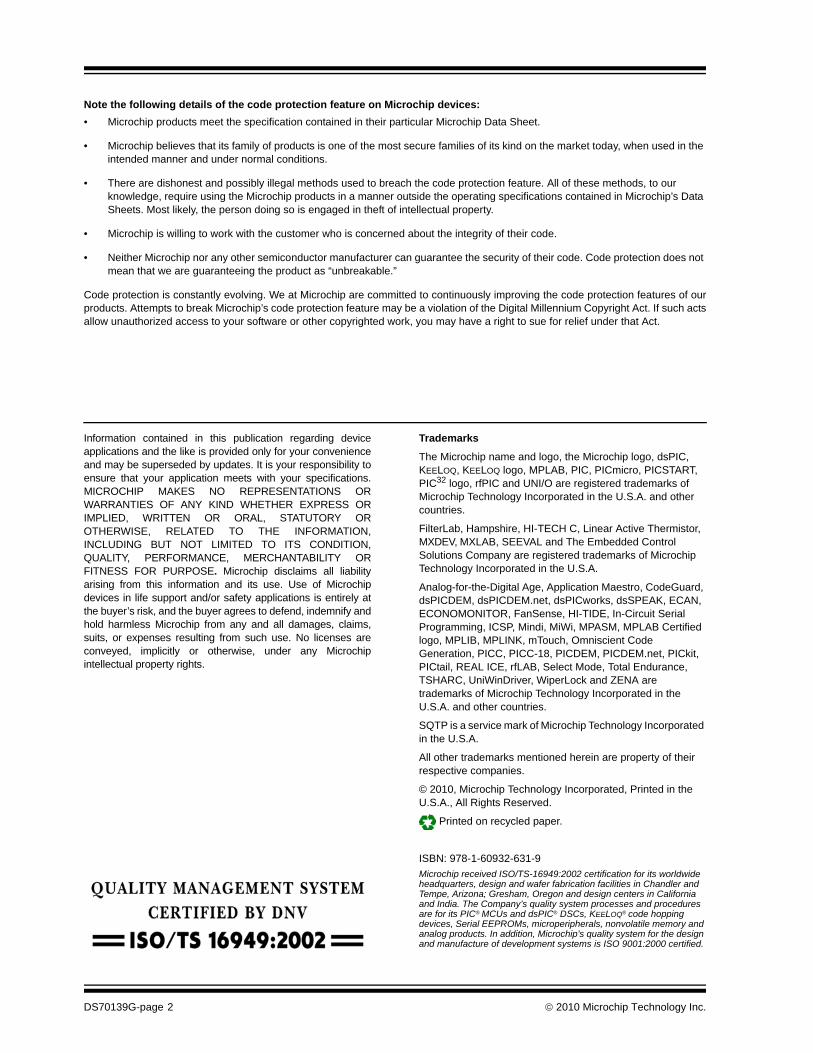
High-Performance Modified RISC CPU:• Modified Harvard architecture• C compiler optimized instruction set architecture• Flexible addressing modes• 83 base instructions• 24-bit wide instructions, 16-bit wide data path• Up to 24 Kbytes on-chip Flash program space• Up to 2 Kbytes of on-chip data RAM• Up to 1 Kbytes of nonvolatile data EEPROM • 16 x 16-bit working register array• Up to 30 MIPS operation:
- DC to 40 MHz external clock input- 4 MHz - 10 MHz oscillator input with
PLL active (4x, 8x, 16x)• Up to 21 interrupt sources:
- 8 user-selectable priority levels- 3 external interrupt sources- 4 processor trap sources
DSP Features:• Dual data fetch• Modulo and Bit-Reversed modes• Two 40-bit wide accumulators with optional
saturation logic• 17-bit x 17-bit single-cycle hardware fractional/
integer multiplier• All DSP instructions are single cycle
- Multiply-Accumulate (MAC) operation• Single-cycle ±16 shift
Peripheral Features:• High-current sink/source I/O pins: 25 mA/25 mA• Three 16-bit timers/counters; optionally pair up
16-bit timers into 32-bit timer modules• 16-bit Capture input functions• 16-bit Compare/PWM output functions• 3-wire SPI modules (supports four Frame modes)• I2C™ module supports Multi-Master/Slave mode
and 7-bit/10-bit addressing• Up to two addressable UART modules with FIFO
buffers
Analog Features:• 12-bit Analog-to-Digital Converter (ADC) with:
- 200 ksps conversion rate- Up to 10 input channels- Conversion available during Sleep and Idle
• Programmable Low-Voltage Detection (PLVD)• Programmable Brown-out Reset
Special Microcontroller Features:• Enhanced Flash program memory:
- 10,000 erase/write cycle (min.) for industrial temperature range, 100K (typical)
• Data EEPROM memory:- 100,000 erase/write cycle (min.) for
industrial temperature range, 1M (typical)• Self-reprogrammable under software control• Power-on Reset (POR), Power-up Timer (PWRT)
and Oscillator Start-up Timer (OST)• Flexible Watchdog Timer (WDT) with on-chip
low-power RC oscillator for reliable operation• Fail-Safe Clock Monitor operation:
- Detects clock failure and switches to on-chip low-power RC oscillator
• Programmable code protection• In-Circuit Serial Programming™ (ICSP™)• Selectable Power Management modes:
- Sleep, Idle and Alternate Clock modes
CMOS Technology:• Low-power, high-speed Flash technology• Wide operating voltage range (2.5V to 5.5V)• Industrial and Extended temperature ranges• Low-power consumption
Note: This data sheet summarizes features ofthis group of dsPIC30F devices and is notintended to be a complete referencesource. For more information on the CPU,peripherals, register descriptions andgeneral device functionality, refer to the“dsPIC30F Family Reference Manual”(DS70046). For more information on thedevice instruction set and programming,refer to the “16-bit MCU and DSCProgrammer’s Reference Manual”(DS70157).
© 2010 Microchip Technology Inc. DS70139G-page 3
dsPIC30F2011/2012/3012/3013
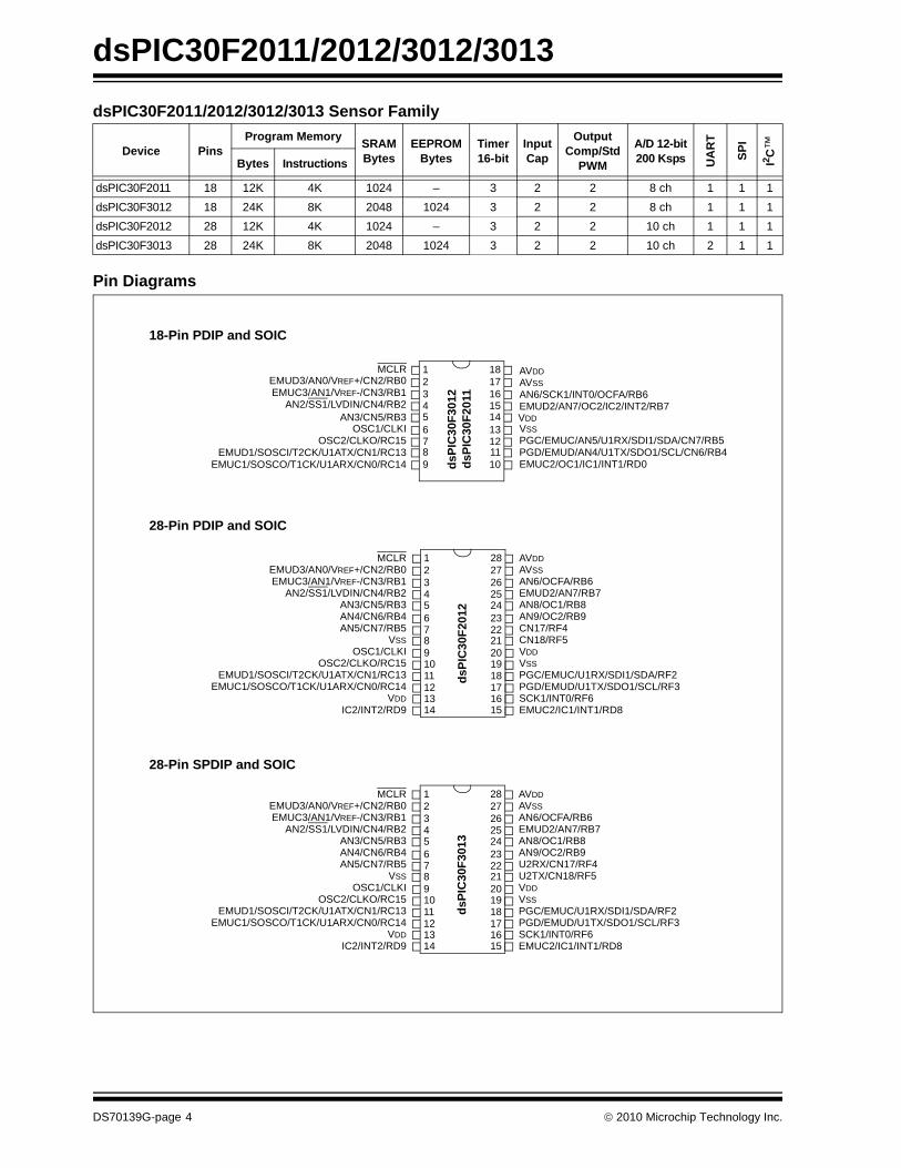
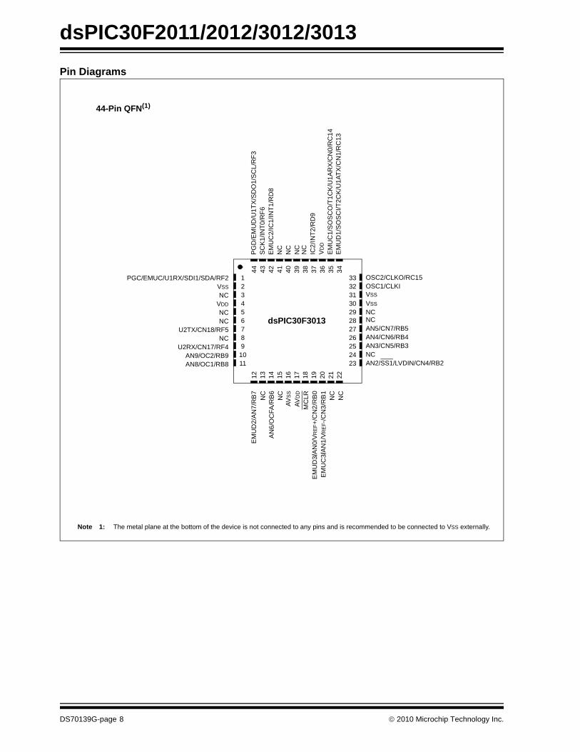
dsPIC30F2011/2012/3012/3013 Sensor FamilyPin Diagrams
Device PinsProgram Memory SRAM
BytesEEPROM
BytesTimer 16-bit
InputCap
Output Comp/Std
PWM
A/D 12-bit 200 Ksps U
AR
T
SPI
I2 C™
Bytes Instructions
dsPIC30F2011 18 12K 4K 1024 – 3 2 2 8 ch 1 1 1dsPIC30F3012 18 24K 8K 2048 1024 3 2 2 8 ch 1 1 1dsPIC30F2012 28 12K 4K 1024 – 3 2 2 10 ch 1 1 1dsPIC30F3013 28 24K 8K 2048 1024 3 2 2 10 ch 2 1 1
EMUD1/SOSCI/T2CK/U1ATX/CN1/RC13EMUC1/SOSCO/T1CK/U1ARX/CN0/RC14
OSC1/CLKIVDD
OSC2/CLKO/RC15PGD/EMUD/AN4/U1TX/SDO1/SCL/CN6/RB4
AVDD
PGC/EMUC/AN5/U1RX/SDI1/SDA/CN7/RB5
EMUD2/AN7/OC2/IC2/INT2/RB7
EMUD3/AN0/VREF+/CN2/RB0
VSS
AN6/SCK1/INT0/OCFA/RB6AVSS
EMUC3/AN1/VREF-/CN3/RB1AN2/SS1/LVDIN/CN4/RB2
123456789
181716151413121110 EMUC2/OC1/IC1/INT1/RD0
18-Pin PDIP and SOIC
dsPI
C30
F201
1ds
PIC
30F3
012
AN3/CN5/RB3
MCLR
28-Pin PDIP and SOIC
MCLR
VSS
VDD
EMUD3/AN0/VREF+/CN2/RB0EMUC3/AN1/VREF-/CN3/RB1
AVDDAVSS
AN2/SS1/LVDIN/CN4/RB2
IC2/INT2/RD9 EMUC2/IC1/INT1/RD8
EMUC1/SOSCO/T1CK/U1ARX/CN0/RC14EMUD1/SOSCI/T2CK/U1ATX/CN1/RC13
VSSOSC2/CLKO/RC15OSC1/CLKI VDD
SCK1/INT0/RF6
PGC/EMUC/U1RX/SDI1/SDA/RF2PGD/EMUD/U1TX/SDO1/SCL/RF3
AN5/CN7/RB5AN4/CN6/RB4AN3/CN5/RB3
1234567891011121314
2827262524232221201918171615
AN6/OCFA/RB6EMUD2/AN7/RB7AN8/OC1/RB8AN9/OC2/RB9CN17/RF4CN18/RF5
dsPI
C30
F201
2
MCLR
VSS
VDD
EMUD3/AN0/VREF+/CN2/RB0EMUC3/AN1/VREF-/CN3/RB1
AVDDAVSS
AN2/SS1/LVDIN/CN4/RB2
IC2/INT2/RD9 EMUC2/IC1/INT1/RD8
EMUC1/SOSCO/T1CK/U1ARX/CN0/RC14EMUD1/SOSCI/T2CK/U1ATX/CN1/RC13
VSSOSC2/CLKO/RC15OSC1/CLKI VDD
SCK1/INT0/RF6
PGC/EMUC/U1RX/SDI1/SDA/RF2PGD/EMUD/U1TX/SDO1/SCL/RF3
AN5/CN7/RB5AN4/CN6/RB4AN3/CN5/RB3
1234567891011121314
2827262524232221201918171615
AN6/OCFA/RB6EMUD2/AN7/RB7AN8/OC1/RB8AN9/OC2/RB9U2RX/CN17/RF4U2TX/CN18/RF5
dsPI
C30
F301
3
28-Pin SPDIP and SOIC
DS70139G-page 4 © 2010 Microchip Technology Inc.
dsPIC30F2011/2012/3012/3013
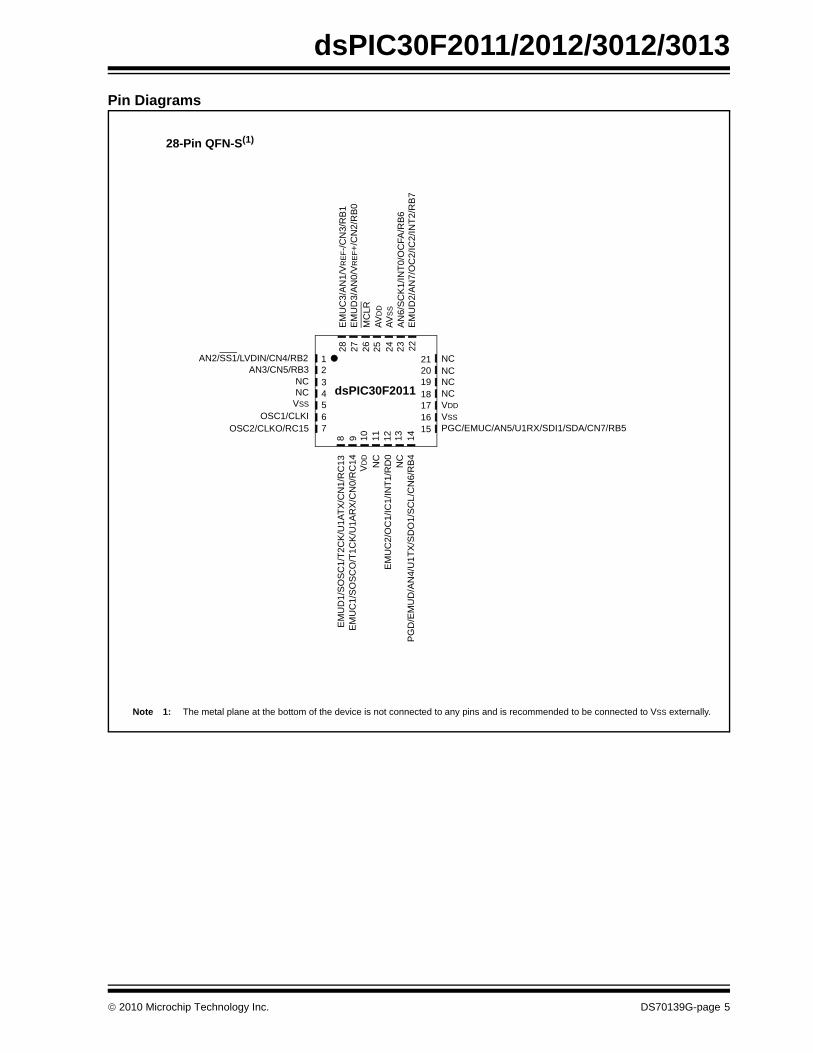
Pin Diagrams28-Pin QFN-S(1)
EMU
C3/
AN1/
VRE
F-/C
N3/
RB
1EM
UD
3/AN
0/V R
EF+
/CN
2/R
B0
MC
LR
28 27 26 25 24 23 22
8 9 10 11 12 13 14
1234567
21201918171615
dsPIC30F2011N
C
NC
NCNCNCNC
NCNC
AVD
DAV
SS
AN6/
SCK
1/IN
T0/O
CFA
/RB6
EMU
D2/
AN7/
OC
2/IC
2/IN
T2/R
B7
VDDVSSPGC/EMUC/AN5/U1RX/SDI1/SDA/CN7/RB5
AN2/SS1/LVDIN/CN4/RB2AN3/CN5/RB3
VSS
OSC1/CLKIOSC2/CLKO/RC15
PG
D/E
MU
D/A
N4/
U1T
X/S
DO
1/SC
L/C
N6/
RB
4
EM
UC
2/O
C1/
IC1/
INT1
/RD
0
EM
UD
1/S
OSC
1/T2
CK
/U1A
TX/C
N1/
RC
13E
MU
C1/
SO
SCO
/T1C
K/U
1AR
X/C
N0/
RC
14V
DD
Note 1: The metal plane at the bottom of the device is not connected to any pins and is recommended to be connected to VSS externally.
© 2010 Microchip Technology Inc. DS70139G-page 5
dsPIC30F2011/2012/3012/3013
Pin Diagrams10 1123
6
1
18192021
22
12 13 1415
8
71617
2324252627289
dsPIC30F2012
EM
UD
1/S
OS
CI/T
2CK
/U1A
TX/C
N1/
RC
13
54
AVD
DA
VSS
AN
6/O
CFA
/RB
6E
MU
D2/
AN
7/R
B7
AN8/OC1/RB8AN9/OC2/RB9CN17/RF4CN18/RF5VDDVSSPGC/EMUC/U1RX/SDI1/SDA/RF2PG
D/E
MU
D/U
1TX/
SD
O1/
SC
L/R
F3S
CK1
/INT0
/RF6
EMU
C2/
IC1/
INT1
/RD
8
MC
LRE
MU
D3/
AN0/
VR
EF+
/CN
2/R
B0
EM
UC
3/AN
1/VR
EF-
/CN
3/R
B1
AN2/SS1/LVDIN/CN4/RB2AN3/CN5/RB3AN4/CN6/RB4AN5/CN7/RB5
VSSOSC1/CLKI
OSC2/CLKO/RC15
EMU
C1/
SOS
CO
/T1C
K/U
1AR
X/C
N0/
RC
14V
DD
IC2/
INT2
/RD
9
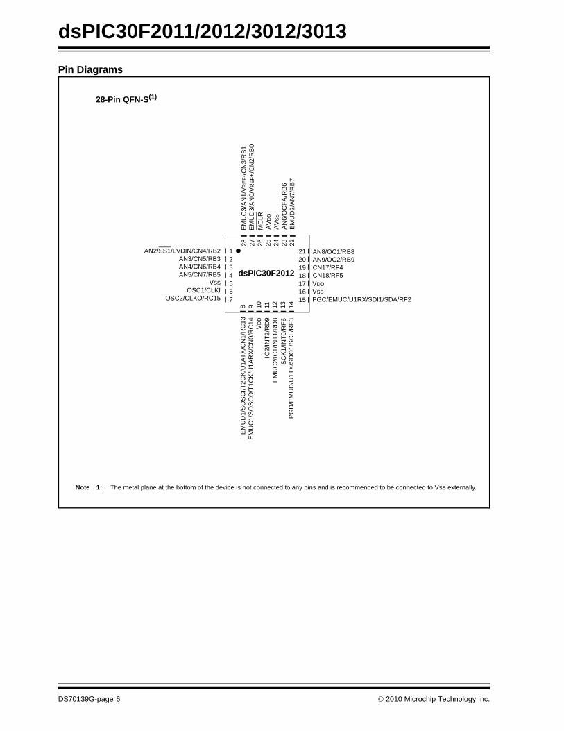
28-Pin QFN-S(1)
Note 1: The metal plane at the bottom of the device is not connected to any pins and is recommended to be connected to VSS externally.
DS70139G-page 6 © 2010 Microchip Technology Inc.
dsPIC30F2011/2012/3012/3013
Pin Diagram44 43 42 41 40 39 38 37 36 35
12 13 14 15 16 17 18 19 20 21
33029282726252423
45
789
1011
12 32
31
NCNCNCNCNC
NCVDDNC
VSSPGC/EMUC/AN5/U1RX/SDI1/SDA/CN7/RB5
NC
NC
EM
UC
3/A
N1/
V RE
F-/C
N3/
RB1
EM
UD
3/A
N0/
V RE
F+/C
N2/
RB0
MC
LRAV
DD
NC
AN6/
SCK
1/IN
T0/O
CFA
/RB6
EM
UD
2/A
N7/
OC
2/IC
2/IN
T2/R
B7
AN2/SS1/LVDIN/CN4/RB2NCAN3/CN5/RB3NCNC
NCVSS
OSC1/CLKIOSC2/CLKO/RC15
PG
D/E
MU
D/A
N4/
U1T
X/S
DO
1/S
CL/
CN
6/R
B4
NC
EM
UC
2/O
C1/
IC1/
INT1
/RD
0N
CN
C
EM
UC
1/S
OS
CO
/T1C
K/U
1AR
X/C
N0/
RC
14
NC
NC
VD
D
6
22
3334
NC
AVS
S
NCN
C
EM
UD
1/S
OS
CI/T
2CK
/U1A
TX/C
N1/
RC
13
VSS
NC
dsPIC30F3012
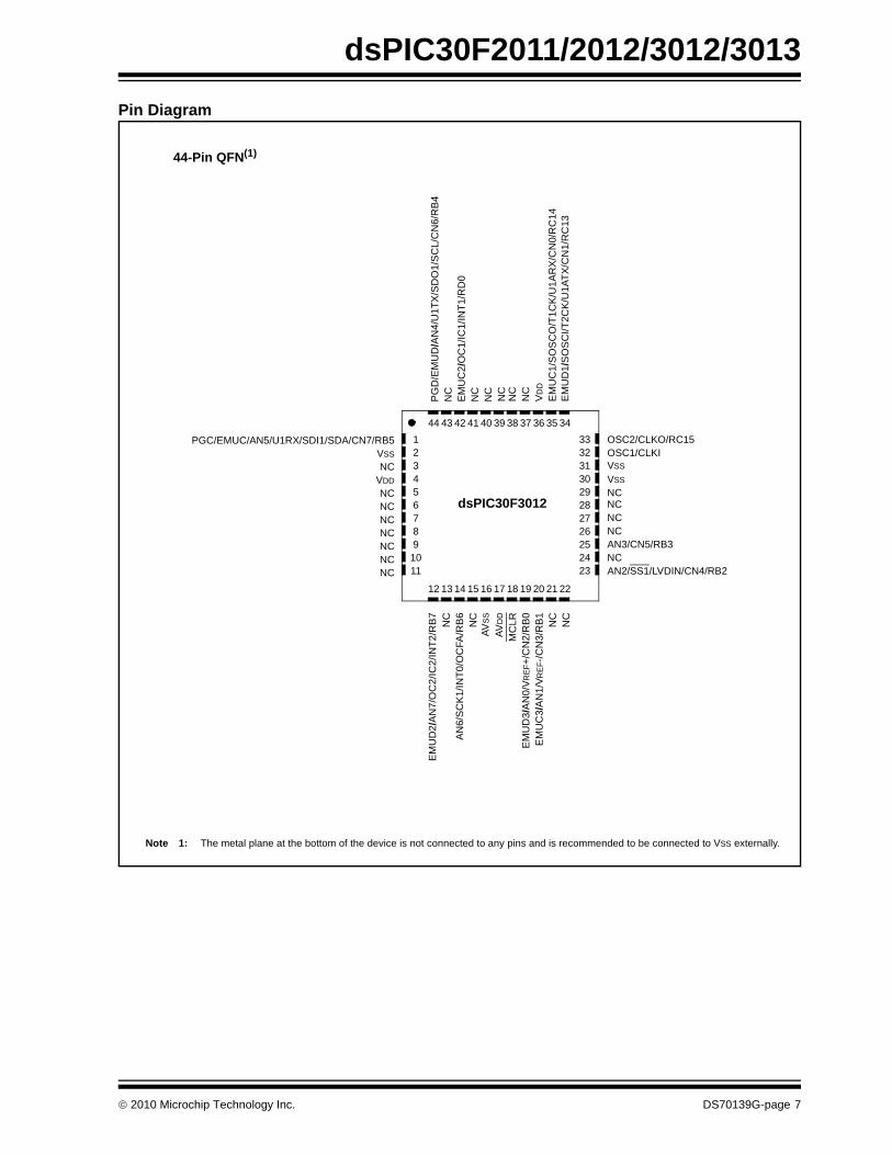
44-Pin QFN(1)
Note 1: The metal plane at the bottom of the device is not connected to any pins and is recommended to be connected to VSS externally.
© 2010 Microchip Technology Inc. DS70139G-page 7
dsPIC30F2011/2012/3012/3013
Pin Diagrams44-Pin QFN(1)
AN8/OC1/RB8AN9/OC2/RB9
U2RX/CN17/RF4NC
U2TX/CN18/RF5
NCVDDNC
VSS PGC/EMUC/U1RX/SDI1/SDA/RF2
NC
NC
EMU
C3/
AN1/
V RE
F-/C
N3/
RB
1E
MU
D3/
AN
0/V R
EF+
/CN
2/R
B0
MC
LRAV
DD
NC
AN
6/O
CFA
/RB
6
EM
UD
2/A
N7/
RB
7
AN2/SS1/LVDIN/CN4/RB2NCAN3/CN5/RB3AN4/CN6/RB4AN5/CN7/RB5
NCVSS
OSC1/CLKIOSC2/CLKO/RC15
PGD
/EM
UD
/U1T
X/S
DO
1/S
CL/
RF3
SCK
1/IN
T0/R
F6EM
UC
2/IC
1/IN
T1/R
D8
NC
NC
EM
UC
1/S
OS
CO
/T1C
K/U
1AR
X/C
N0/
RC
14
NC
IC2/
INT2
/RD
9V
DD
NC
AVS
S
NC
NC
EM
UD
1/S
OS
CI/T
2CK/
U1A
TX/C
N1/
RC
13
VSS
NC
dsPIC30F3013
44 43 42 41 40 39 38 37 36 35
12 13 14 15 16 17 18 19 20 21
33029282726252423
45
789
1011
12 32
31
6
22
33
34
Note 1: The metal plane at the bottom of the device is not connected to any pins and is recommended to be connected to VSS externally.
DS70139G-page 8 © 2010 Microchip Technology Inc.
dsPIC30F2011/2012/3012/3013
Table of Contents1.0 Device Overview ........................................................................................................................................................................ 112.0 CPU Architecture Overview........................................................................................................................................................ 193.0 Memory Organization ................................................................................................................................................................. 294.0 Address Generator Units............................................................................................................................................................ 435.0 Flash Program Memory.............................................................................................................................................................. 496.0 Data EEPROM Memory ............................................................................................................................................................. 557.0 I/O Ports ..................................................................................................................................................................................... 598.0 Interrupts .................................................................................................................................................................................... 659.0 Timer1 Module ........................................................................................................................................................................... 7310.0 Timer2/3 Module ........................................................................................................................................................................ 7711.0 Input Capture Module................................................................................................................................................................. 8312.0 Output Compare Module ............................................................................................................................................................ 8713.0 SPI™ Module ............................................................................................................................................................................. 9314.0 I2C™ Module ............................................................................................................................................................................. 9715.0 Universal Asynchronous Receiver Transmitter (UART) Module .............................................................................................. 10516.0 12-bit Analog-to-Digital Converter (ADC) Module .................................................................................................................... 11317.0 System Integration ................................................................................................................................................................... 12318.0 Instruction Set Summary .......................................................................................................................................................... 13719.0 Development Support............................................................................................................................................................... 14520.0 Electrical Characteristics .......................................................................................................................................................... 14921.0 Packaging Information.............................................................................................................................................................. 187Index .................................................................................................................................................................................................. 201The Microchip Web Site..................................................................................................................................................................... 207Customer Change Notification Service .............................................................................................................................................. 207Customer Support .............................................................................................................................................................................. 207Reader Response .............................................................................................................................................................................. 208Product Identification System ............................................................................................................................................................ 209
TO OUR VALUED CUSTOMERSIt is our intention to provide our valued customers with the best documentation possible to ensure successful use of your Microchipproducts. To this end, we will continue to improve our publications to better suit your needs. Our publications will be refined andenhanced as new volumes and updates are introduced. If you have any questions or comments regarding this publication, please contact the Marketing Communications Department viaE-mail at [email protected] or fax the Reader Response Form in the back of this data sheet to (480) 792-4150. Wewelcome your feedback.
Most Current Data SheetTo obtain the most up-to-date version of this data sheet, please register at our Worldwide Web site at:
http://www.microchip.comYou can determine the version of a data sheet by examining its literature number found on the bottom outside corner of any page.The last character of the literature number is the version number, (e.g., DS30000A is version A of document DS30000).
ErrataAn errata sheet, describing minor operational differences from the data sheet and recommended workarounds, may exist for currentdevices. As device/documentation issues become known to us, we will publish an errata sheet. The errata will specify the revision ofsilicon and revision of document to which it applies.To determine if an errata sheet exists for a particular device, please check with one of the following:• Microchip’s Worldwide Web site; http://www.microchip.com• Your local Microchip sales office (see last page)When contacting a sales office, please specify which device, revision of silicon and data sheet (include literature number) you areusing.
Customer Notification SystemRegister on our web site at www.microchip.com to receive the most current information on all of our products.
© 2010 Microchip Technology Inc. DS70139G-page 9

dsPIC30F2011/2012/3012/3013
NOTES:DS70139G-page 10 © 2010 Microchip Technology Inc.
dsPIC30F2011/2012/3012/3013
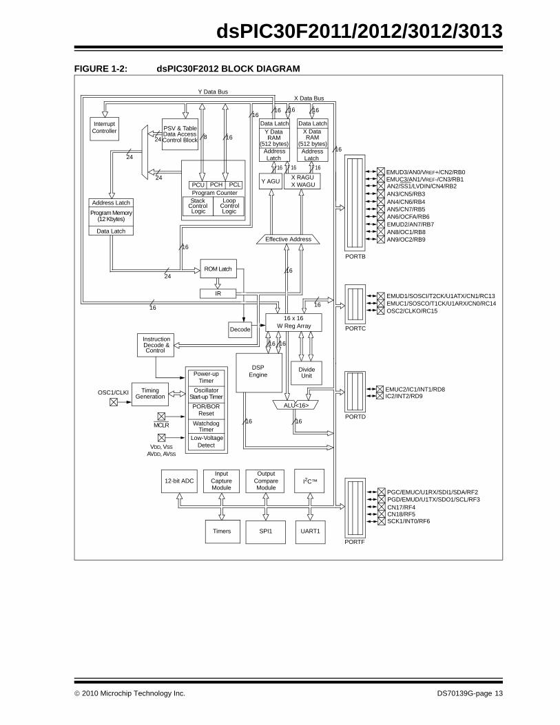
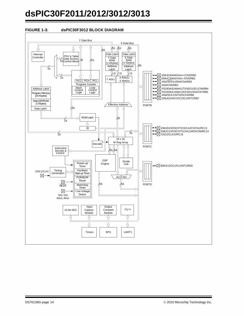
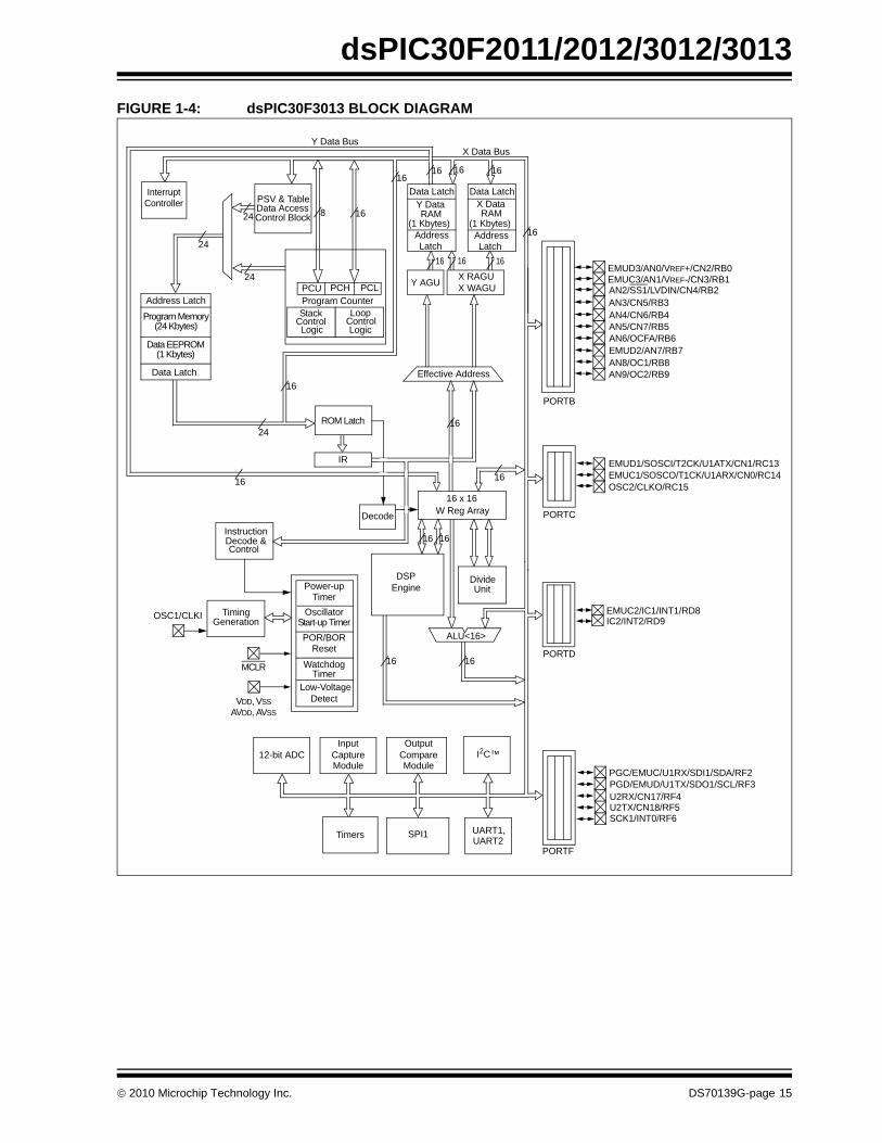
1.0 DEVICE OVERVIEW
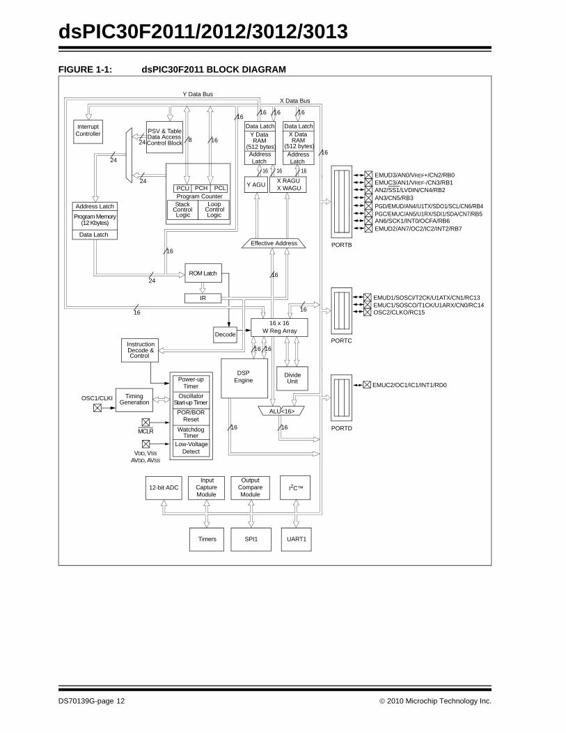
This data sheet contains information specific to thedsPIC30F2011, dsPIC30F2012, dsPIC30F3012 anddsPIC30F3013 Digital Signal Controllers (DSC). Thesedevices contain extensive Digital Signal Processor(DSP) functionality within a high-performance 16-bitmicrocontroller (MCU) architecture.
The following block diagrams depict the architecture forthese devices:
• Figure 1-1 illustrates the dsPIC30F2011• Figure 1-2 illustrates the dsPIC30F2012• Figure 1-3 illustrates the dsPIC30F3012• Figure 1-4 illustrates the dsPIC30F3013
Following the block diagrams, Table 1-1 relates the I/Ofunctions to pinout information.
Note: This data sheet summarizes features ofthis group of dsPIC30F devices and is notintended to be a complete referencesource. For more information on the CPU,peripherals, register descriptions andgeneral device functionality, refer to the“dsPIC30F Family Reference Manual”(DS70046). For more information on thedevice instruction set and programming,refer to the “16-bit MCU and DSCProgrammer’s Reference Manual”(DS70157).
© 2010 Microchip Technology Inc. DS70139G-page 11
dsPIC30F2011/2012/3012/3013
FIGURE 1-1: dsPIC30F2011 BLOCK DIAGRAMPower-upTimer
OscillatorStart-up TimerPOR/BOR
ResetWatchdog
Timer
InstructionDecode &Control
OSC1/CLKI
MCLR
VDD, VSS
PGD/EMUD/AN4/U1TX/SDO1/SCL/CN6/RB4
Low-VoltageDetect
UART1
TimingGeneration
PGC/EMUC/AN5/U1RX/SDI1/SDA/CN7/RB5
16
PCH PCLProgram Counter
ALU<16>
16
24
24
24
24
X Data Bus
IR
I2C™
AN6/SCK1/INT0/OCFA/RB6EMUD2/AN7/OC2/IC2/INT2/RB7
PCU
12-bit ADC
Timers
InputCaptureModule
OutputCompareModule
EMUC1/SOSCO/T1CK/U1ARX/CN0/RC14EMUD1/SOSCI/T2CK/U1ATX/CN1/RC13
PORTB
PORTD
16
16 16
16 x 16W Reg Array
Divide Unit Engine
DSP
Decode
ROM Latch
16
Y Data Bus
Effective Address
X RAGUX WAGU Y AGU
EMUD3/AN0/VREF+/CN2/RB0EMUC3/AN1/VREF-/CN3/RB1AN2/SS1/LVDIN/CN4/RB2AN3/CN5/RB3
OSC2/CLKO/RC15
AVDD, AVSS
16
16
16
16
16
PORTC
16
16
16
16
8
InterruptController PSV & Table
Data AccessControl Block
StackControl Logic
LoopControlLogic
Data LatchData LatchY Data
(512 bytes)RAM
X Data
(512 bytes)RAM
AddressLatch
AddressLatch
EMUC2/OC1/IC1/INT1/RD0
16
SPI1
Address Latch
Program Memory(12 Kbytes)
Data Latch
16
DS70139G-page 12 © 2010 Microchip Technology Inc.
dsPIC30F2011/2012/3012/3013
FIGURE 1-2: dsPIC30F2012 BLOCK DIAGRAMAN8/OC1/RB8AN9/OC2/RB9
Power-upTimer
OscillatorStart-up TimerPOR/BOR
ResetWatchdog
Timer
InstructionDecode &Control
OSC1/CLKI
MCLR
VDD, VSS
AN4/CN6/RB4
Low-VoltageDetect
UART1
TimingGeneration
AN5/CN7/RB5
16
PCH PCLProgram Counter
ALU<16>
16
24
24
24
24
X Data Bus
IR
I2C™
AN6/OCFA/RB6EMUD2/AN7/RB7
PCU
12-bit ADC
Timers
CN18/RF5SCK1/INT0/RF6
InputCaptureModule
OutputCompareModule
EMUC1/SOSCO/T1CK/U1ARX/CN0/RC14EMUD1/SOSCI/T2CK/U1ATX/CN1/RC13
EMUD3/AN0/VREF+/CN2/RB0
PORTB
PGC/EMUC/U1RX/SDI1/SDA/RF2PGD/EMUD/U1TX/SDO1/SCL/RF3
PORTD
16
16 16
16 x 16W Reg Array
Divide Unit Engine
DSP
Decode
ROM Latch
16
Y Data Bus
Effective Address
X RAGUX WAGU Y AGU
AN2/SS1/LVDIN/CN4/RB2AN3/CN5/RB3
OSC2/CLKO/RC15
CN17/RF4
AVDD, AVSS
16
16
16
16
16
PORTC
PORTF
16
16
16
16
8
InterruptController PSV & Table
Data AccessControl Block
StackControl Logic
LoopControlLogic
Data LatchData LatchY Data
(512 bytes)RAM
X Data RAM
AddressLatch
AddressLatch
EMUC2/IC1/INT1/RD8IC2/INT2/RD9
16
EMUC3/AN1/VREF-/CN3/RB1
SPI1
Address Latch
Program Memory(12 Kbytes)
Data Latch
16(512 bytes)
© 2010 Microchip Technology Inc. DS70139G-page 13
dsPIC30F2011/2012/3012/3013
FIGURE 1-3: dsPIC30F3012 BLOCK DIAGRAMPower-upTimer
OscillatorStart-up TimerPOR/BOR
ResetWatchdog
Timer
InstructionDecode &Control
OSC1/CLKI
MCLR
VDD, VSS
PGD/EMUD/AN4/U1TX/SDO1/SCL/CN6/RB4
Low-VoltageDetect
UART1
TimingGeneration
PGC/EMUC/AN5/U1RX/SDI1/SDA/CN7/RB5
16
PCH PCLProgram Counter
ALU<16>
16
24
24
24
24
X Data Bus
IR
I2C™
AN6/SCK1/INT0/OCFA/RB6EMUD2/AN7/OC2/IC2/INT2/RB7
PCU
12-bit ADC
Timers
InputCaptureModule
OutputCompareModule
EMUC1/SOSCO/T1CK/U1ARX/CN0/RC14EMUD1/SOSCI/T2CK/U1ATX/CN1/RC13
PORTB
PORTD
16
16 16
16 x 16W Reg Array
Divide Unit Engine
DSP
Decode
ROM Latch
16
Y Data Bus
Effective Address
X RAGUX WAGU Y AGU
EMUD3/AN0/VREF+/CN2/RB0EMUC3/AN1/VREF-/CN3/RB1AN2/SS1/LVDIN/CN4/RB2AN3/CN5/RB3
OSC2/CLKO/RC15
AVDD, AVSS
16
16
16
16
16
PORTC
16
16
16
16
8
InterruptController PSV & Table
Data AccessControl Block
StackControl Logic
LoopControlLogic
Data LatchData LatchY Data
(1 Kbytes)RAM
X Data
(1 Kbytes)RAM
AddressLatch
AddressLatch
EMUC2/OC1/IC1/INT1/RD0
16
SPI1
Address Latch
Program Memory(24 Kbytes)
Data Latch
16
Data EEPROM(1 Kbytes)
DS70139G-page 14 © 2010 Microchip Technology Inc.
dsPIC30F2011/2012/3012/3013
FIGURE 1-4: dsPIC30F3013 BLOCK DIAGRAMAN8/OC1/RB8AN9/OC2/RB9
Power-upTimer
OscillatorStart-up TimerPOR/BOR
ResetWatchdog
Timer
InstructionDecode &Control
OSC1/CLKI
MCLR
VDD, VSS
AN4/CN6/RB4
Low-VoltageDetect
UART1,
TimingGeneration
AN5/CN7/RB5
16
PCH PCLProgram Counter
ALU<16>
16
24
24
24
24
X Data Bus
IR
I2C™
AN6/OCFA/RB6EMUD2/AN7/RB7
PCU
12-bit ADC
Timers
U2TX/CN18/RF5SCK1/INT0/RF6
InputCaptureModule
OutputCompareModule
EMUC1/SOSCO/T1CK/U1ARX/CN0/RC14EMUD1/SOSCI/T2CK/U1ATX/CN1/RC13
EMUD3/AN0/VREF+/CN2/RB0
PORTB
PGC/EMUC/U1RX/SDI1/SDA/RF2PGD/EMUD/U1TX/SDO1/SCL/RF3
PORTD
16
16 16
16 x 16W Reg Array
Divide Unit Engine
DSP
Decode
ROM Latch
16
Y Data Bus
Effective Address
X RAGUX WAGU Y AGU
AN2/SS1/LVDIN/CN4/RB2AN3/CN5/RB3
OSC2/CLKO/RC15
U2RX/CN17/RF4
AVDD, AVSS
UART2
16
16
16
16
16
PORTC
PORTF
16
16
16
16
8
InterruptController PSV & Table
Data AccessControl Block
StackControl Logic
LoopControlLogic
Data LatchData LatchY Data
(1 Kbytes)RAM
X Data RAM
AddressLatch
AddressLatch
EMUC2/IC1/INT1/RD8IC2/INT2/RD9
16
EMUC3/AN1/VREF-/CN3/RB1
SPI1
16(1 Kbytes)
Address Latch
Program Memory(24 Kbytes)
Data Latch
Data EEPROM(1 Kbytes)
© 2010 Microchip Technology Inc. DS70139G-page 15
dsPIC30F2011/2012/3012/3013
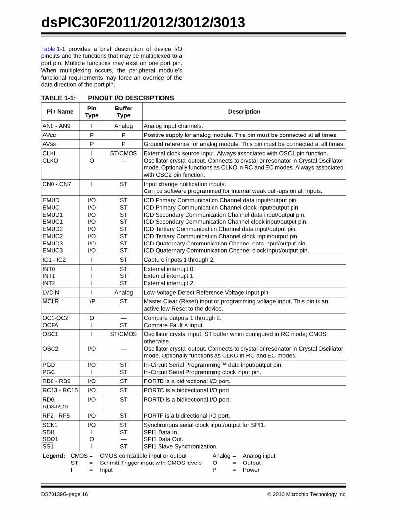
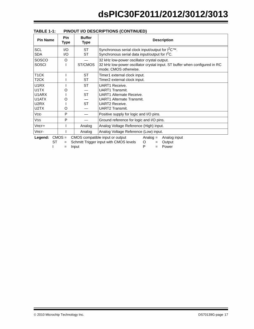
Table 1-1 provides a brief description of device I/Opinouts and the functions that may be multiplexed to aport pin. Multiple functions may exist on one port pin.When multiplexing occurs, the peripheral module’sfunctional requirements may force an override of thedata direction of the port pin.TABLE 1-1: PINOUT I/O DESCRIPTIONS
Pin Name PinType
BufferType Description
AN0 - AN9 I Analog Analog input channels. AVDD P P Positive supply for analog module. This pin must be connected at all times.AVSS P P Ground reference for analog module. This pin must be connected at all times.CLKICLKO
IO
ST/CMOS—
External clock source input. Always associated with OSC1 pin function.Oscillator crystal output. Connects to crystal or resonator in Crystal Oscillator mode. Optionally functions as CLKO in RC and EC modes. Always associated with OSC2 pin function.
CN0 - CN7 I ST Input change notification inputs.Can be software programmed for internal weak pull-ups on all inputs.
EMUDEMUCEMUD1EMUC1EMUD2EMUC2EMUD3EMUC3
I/OI/OI/OI/OI/OI/OI/OI/O
STSTSTSTSTSTSTST
ICD Primary Communication Channel data input/output pin.ICD Primary Communication Channel clock input/output pin.ICD Secondary Communication Channel data input/output pin.ICD Secondary Communication Channel clock input/output pin.ICD Tertiary Communication Channel data input/output pin.ICD Tertiary Communication Channel clock input/output pin.ICD Quaternary Communication Channel data input/output pin.ICD Quaternary Communication Channel clock input/output pin.
IC1 - IC2 I ST Capture inputs 1 through 2.INT0INT1INT2
III
STSTST
External interrupt 0.External interrupt 1.External interrupt 2.
LVDIN I Analog Low-Voltage Detect Reference Voltage Input pin.MCLR I/P ST Master Clear (Reset) input or programming voltage input. This pin is an
active-low Reset to the device.OC1-OC2OCFA
OI
—ST
Compare outputs 1 through 2.Compare Fault A input.
OSC1
OSC2
I
I/O
ST/CMOS
—
Oscillator crystal input. ST buffer when configured in RC mode; CMOS otherwise.Oscillator crystal output. Connects to crystal or resonator in Crystal Oscillator mode. Optionally functions as CLKO in RC and EC modes.
PGDPGC
I/OI
STST
In-Circuit Serial Programming™ data input/output pin.In-Circuit Serial Programming clock input pin.
RB0 - RB9 I/O ST PORTB is a bidirectional I/O port.RC13 - RC15 I/O ST PORTC is a bidirectional I/O port.RD0, RD8-RD9
I/O ST PORTD is a bidirectional I/O port.
RF2 - RF5 I/O ST PORTF is a bidirectional I/O port.SCK1SDI1SDO1SS1
I/OIOI
STST—ST
Synchronous serial clock input/output for SPI1.SPI1 Data In.SPI1 Data Out.SPI1 Slave Synchronization.
Legend: CMOS = CMOS compatible input or output Analog = Analog inputST = Schmitt Trigger input with CMOS levels O = Output I = Input P = Power
DS70139G-page 16 © 2010 Microchip Technology Inc.
dsPIC30F2011/2012/3012/3013
SCLSDA
I/OI/O
STST
Synchronous serial clock input/output for I2C™.Synchronous serial data input/output for I2C.
SOSCOSOSCI
OI
—ST/CMOS
32 kHz low-power oscillator crystal output. 32 kHz low-power oscillator crystal input. ST buffer when configured in RC mode; CMOS otherwise.
T1CKT2CK
II
STST
Timer1 external clock input.Timer2 external clock input.
U1RXU1TXU1ARXU1ATXU2RXU2TX
IOIOIO
ST—ST—ST—
UART1 Receive.UART1 Transmit.UART1 Alternate Receive.UART1 Alternate Transmit.UART2 Receive.UART2 Transmit.
VDD P — Positive supply for logic and I/O pins.VSS P — Ground reference for logic and I/O pins.VREF+ I Analog Analog Voltage Reference (High) input.VREF- I Analog Analog Voltage Reference (Low) input.
TABLE 1-1: PINOUT I/O DESCRIPTIONS (CONTINUED)
Pin Name PinType
BufferType Description
Legend: CMOS = CMOS compatible input or output Analog = Analog inputST = Schmitt Trigger input with CMOS levels O = Output I = Input P = Power
© 2010 Microchip Technology Inc. DS70139G-page 17

dsPIC30F2011/2012/3012/3013
NOTES:DS70139G-page 18 © 2010 Microchip Technology Inc.
dsPIC30F2011/2012/3012/3013
2.0 CPU ARCHITECTURE OVERVIEW
This section is an overview of the CPU architecture ofthe dsPIC30F. The core has a 24-bit instruction word.The Program Counter (PC) is 23 bits wide with theLeast Significant bit (LSb) always clear (seeSection 3.1 “Program Address Space”). The MostSignificant bit (MSb) is ignored during normal programexecution, except for certain specialized instructions.Thus, the PC can address up to 4M instruction wordsof user program space. An instruction prefetchmechanism helps maintain throughput. Program loopconstructs, free from loop count managementoverhead, are supported using the DO and REPEATinstructions, both of which are interruptible at any point.
2.1 Core OverviewThe working register array consists of 16 x 16-bitregisters, each of which can act as data, address oroffset registers. One working register (W15) operatesas a Software Stack Pointer for interrupts and calls.
The data space is 64 Kbytes (32K words) and is splitinto two blocks, referred to as X and Y data memory.Each block has its own independent Address Genera-tion Unit (AGU). Most instructions operate solelythrough the X memory, AGU, which provides theappearance of a single unified data space. TheMultiply-Accumulate (MAC) class of dual source DSPinstructions operate through both the X and Y AGUs,splitting the data address space into two parts (seeSection 3.2 “Data Address Space”). The X and Ydata space boundary is device specific and cannot bealtered by the user. Each data word consists of 2 bytesand most instructions can address data either as wordsor bytes.
Two ways to access data in program memory are:
• The upper 32 Kbytes of data space memory can be mapped into the lower half (user space) of program space at any 16K program word boundary, defined by the 8-bit Program Space Visibility Page register (PSVPAG). Thus any instruction can access program space as if it were data space, with a limitation that the access requires an additional cycle. Only the lower 16 bits of each instruction word can be accessed using this method.
• Linear indirect access of 32K word pages within program space is also possible using any working register, via table read and write instructions. Table read and write instructions can be used to access all 24 bits of an instruction word.
Overhead-free circular buffers (Modulo Addressing)are supported in both X and Y address spaces. This isprimarily intended to remove the loop overhead forDSP algorithms.
The X AGU also supports Bit-Reversed Addressing on destination effective addresses to greatly simplify input or output data reordering for radix-2 FFT algorithms. Refer to Section 4.0 “Address Generator Units” for details on Modulo and Bit-Reversed Addressing.
The core supports Inherent (no operand), Relative,Literal, Memory Direct, Register Direct, RegisterIndirect, Register Offset and Literal Offset Addressingmodes. Instructions are associated with pre-definedaddressing modes, depending upon their functionalrequirements.
For most instructions, the core is capable of executinga data (or program data) memory read, a workingregister (data) read, a data memory write and aprogram (instruction) memory read per instructioncycle. As a result, 3 operand instructions aresupported, allowing C = A+B operations to be exe-cuted in a single cycle.
A DSP engine has been included to significantlyenhance the core arithmetic capability and throughput.It features a high-speed 17-bit by 17-bit multiplier, a40-bit ALU, two 40-bit saturating accumulators and a40-bit bidirectional barrel shifter. Data in theaccumulator or any working register can be shifted upto 15 bits right, or 16 bits left in a single cycle. The DSPinstructions operate seamlessly with all otherinstructions and have been designed for optimalreal-time performance. The MAC class of instructionscan concurrently fetch two data operands from memorywhile multiplying two W registers. To enable thisconcurrent fetching of data operands, the data spacehas been split for these instructions and linear is for allothers. This has been achieved in a transparent andflexible manner, by dedicating certain working registersto each address space for the MAC class ofinstructions.
Note: This data sheet summarizes features ofthis group of dsPIC30F devices and is notintended to be a complete referencesource. For more information on the CPU,peripherals, register descriptions andgeneral device functionality, refer to the“dsPIC30F Family Reference Manual”(DS70046). For more information on thedevice instruction set and programming,refer to the “16-bit MCU and DSCProgrammer’s Reference Manual”(DS70157).
© 2010 Microchip Technology Inc. DS70139G-page 19
dsPIC30F2011/2012/3012/3013
The core does not support a multi-stage instructionpipeline. However, a single-stage instruction prefetchmechanism is used, which accesses and partiallydecodes instructions a cycle ahead of execution, inorder to maximize available execution time. Mostinstructions execute in a single cycle with certainexceptions.The core features a vectored exception processingstructure for traps and interrupts, with 62 independentvectors. The exceptions consist of up to 8 traps (ofwhich 4 are reserved) and 54 interrupts. Each interruptis prioritized based on a user-assigned priority between1 and 7 (1 being the lowest priority and 7 being thehighest), in conjunction with a predetermined ‘naturalorder’. Traps have fixed priorities ranging from 8 to 15.
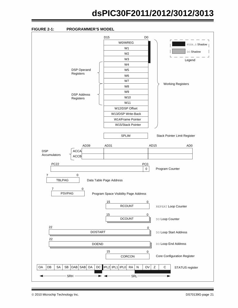
2.2 Programmer’s ModelThe programmer’s model is shown in Figure 2-1 andconsists of 16 x 16-bit working registers (W0 throughW15), 2 x 40-bit accumulators (ACCA and ACCB),STATUS register (SR), Data Table Page register(TBLPAG), Program Space Visibility Page register(PSVPAG), DO and REPEAT registers (DOSTART,DOEND, DCOUNT and RCOUNT) and Program Coun-ter (PC). The working registers can act as data,address or offset registers. All registers are memorymapped. W0 acts as the W register for file registeraddressing.
Some of these registers have a shadow register asso-ciated with each of them, as shown in Figure 2-1. Theshadow register is used as a temporary holding registerand can transfer its contents to or from its host registerupon the occurrence of an event. None of the shadowregisters are accessible directly. The following rulesapply for transfer of registers into and out of shadows.
• PUSH.S and POP.S W0, W1, W2, W3, SR (DC, N, OV, Z and C bits only) are transferred.
• DO instruction DOSTART, DOEND, DCOUNT shadows are pushed on loop start and popped on loop end.
When a byte operation is performed on a working reg-ister, only the Least Significant Byte (LSB) of the targetregister is affected. However, a benefit of memorymapped working registers is that both the Least andMost Significant Bytes (MSB) can be manipulatedthrough byte-wide data memory space accesses.
2.2.1 SOFTWARE STACK POINTER/ FRAME POINTER
The dsPIC® DSC devices contain a software stack.W15 is the dedicated Software Stack Pointer (SP),which is automatically modified by exceptionprocessing and subroutine calls and returns. However,W15 can be referenced by any instruction in the samemanner as all other W registers. This simplifies thereading, writing and manipulation of the Stack Pointer(e.g., creating stack frames).
W15 is initialized to 0x0800 during a Reset. The usermay reprogram the SP during initialization to anylocation within data space.
W14 has been dedicated as a Stack Frame Pointer, asdefined by the LNK and ULNK instructions. However,W14 can be referenced by any instruction in the samemanner as all other W registers.
2.2.2 STATUS REGISTERThe dsPIC DSC core has a 16-bit STATUS register(SR), the LSB of which is referred to as the SR Lowbyte (SRL) and the MSB as the SR High byte (SRH).See Figure 2-1 for SR layout.
SRL contains all the MCU ALU operation Status flags(including the Z bit), as well as the CPU InterruptPriority Level Status bits, IPL<2:0>, and the RepeatActive Status bit, RA. During exception processing,SRL is concatenated with the MSB of the PC to form acomplete word value which is then stacked.
The upper byte of the STATUS register contains theDSP Adder/Subtracter Status bits, the DO Loop Activebit (DA) and the Digit Carry (DC) Status bit.
2.2.3 PROGRAM COUNTERThe program counter is 23 bits wide; bit 0 is alwaysclear. Therefore, the PC can address up to 4Minstruction words.
Note: In order to protect against misalignedstack accesses, W15<0> is always clear.
DS70139G-page 20 © 2010 Microchip Technology Inc.
dsPIC30F2011/2012/3012/3013
FIGURE 2-1: PROGRAMMER’S MODELTABPAG
PC22 PC0
7 0
D0D15
Program Counter
Data Table Page Address
STATUS register
Working Registers
DSP OperandRegisters
W1
W2
W3
W4
W5
W6W7
W8
W9
W10
W11
W12/DSP Offset
W13/DSP Write-Back
W14/Frame Pointer
W15/Stack Pointer
DSP AddressRegisters
AD39 AD0AD31
DSPAccumulators
ACCAACCB
PSVPAG7 0
Program Space Visibility Page Address
Z
0
OA OB SA SB
RCOUNT15 0
REPEAT Loop Counter
DCOUNT15 0
DO Loop Counter
DOSTART 22 0
DO Loop Start Address
IPL2 IPL1
SPLIM Stack Pointer Limit Register
AD15
SRL
PUSH.S Shadow
DO Shadow
OAB SAB
15 0Core Configuration Register
Legend
CORCON
DA DC RA N
TBLPAG
PSVPAG
IPL0 OV
W0/WREG
SRH
DO Loop End AddressDOEND 22
C
© 2010 Microchip Technology Inc. DS70139G-page 21
dsPIC30F2011/2012/3012/3013
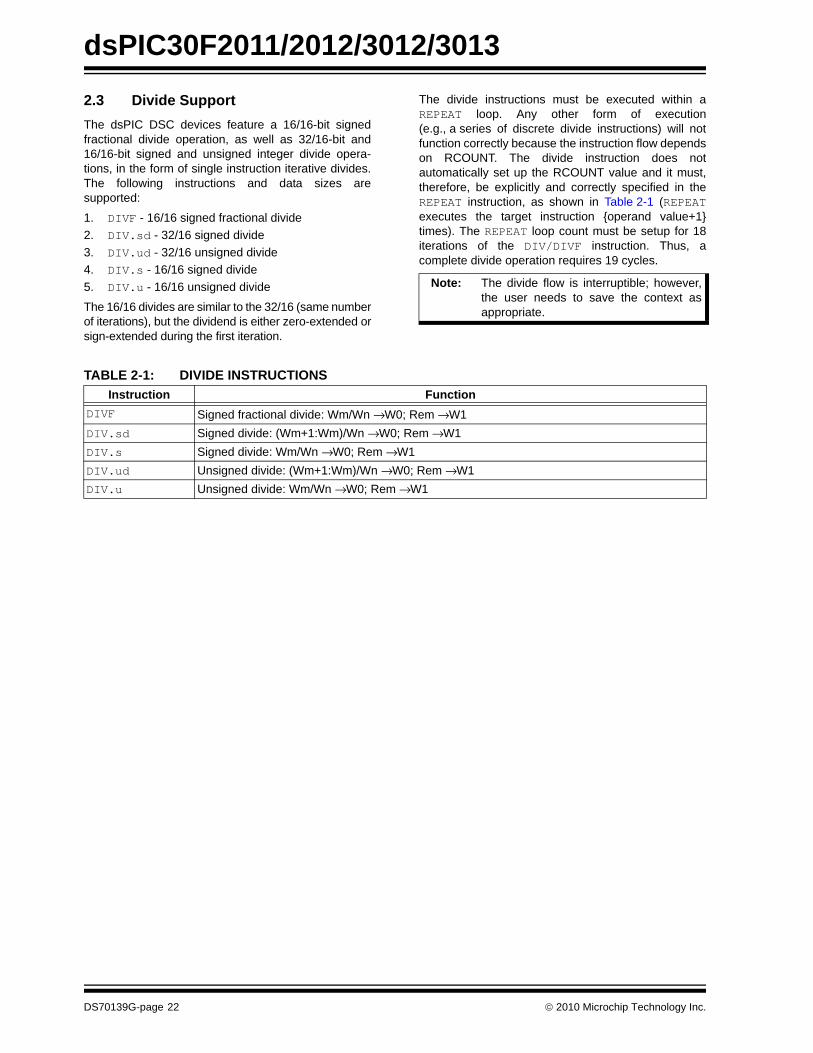
2.3 Divide SupportThe dsPIC DSC devices feature a 16/16-bit signedfractional divide operation, as well as 32/16-bit and16/16-bit signed and unsigned integer divide opera-tions, in the form of single instruction iterative divides.The following instructions and data sizes aresupported:1. DIVF - 16/16 signed fractional divide2. DIV.sd - 32/16 signed divide3. DIV.ud - 32/16 unsigned divide4. DIV.s - 16/16 signed divide5. DIV.u - 16/16 unsigned divide
The 16/16 divides are similar to the 32/16 (same numberof iterations), but the dividend is either zero-extended orsign-extended during the first iteration.
The divide instructions must be executed within aREPEAT loop. Any other form of execution(e.g., a series of discrete divide instructions) will notfunction correctly because the instruction flow dependson RCOUNT. The divide instruction does notautomatically set up the RCOUNT value and it must,therefore, be explicitly and correctly specified in theREPEAT instruction, as shown in Table 2-1 (REPEATexecutes the target instruction {operand value+1}times). The REPEAT loop count must be setup for 18iterations of the DIV/DIVF instruction. Thus, acomplete divide operation requires 19 cycles.
TABLE 2-1: DIVIDE INSTRUCTIONS
Note: The divide flow is interruptible; however,the user needs to save the context asappropriate.
Instruction FunctionDIVF Signed fractional divide: Wm/Wn → W0; Rem → W1DIV.sd Signed divide: (Wm+1:Wm)/Wn → W0; Rem → W1DIV.s Signed divide: Wm/Wn → W0; Rem → W1DIV.ud Unsigned divide: (Wm+1:Wm)/Wn → W0; Rem → W1DIV.u Unsigned divide: Wm/Wn → W0; Rem → W1
DS70139G-page 22 © 2010 Microchip Technology Inc.
dsPIC30F2011/2012/3012/3013
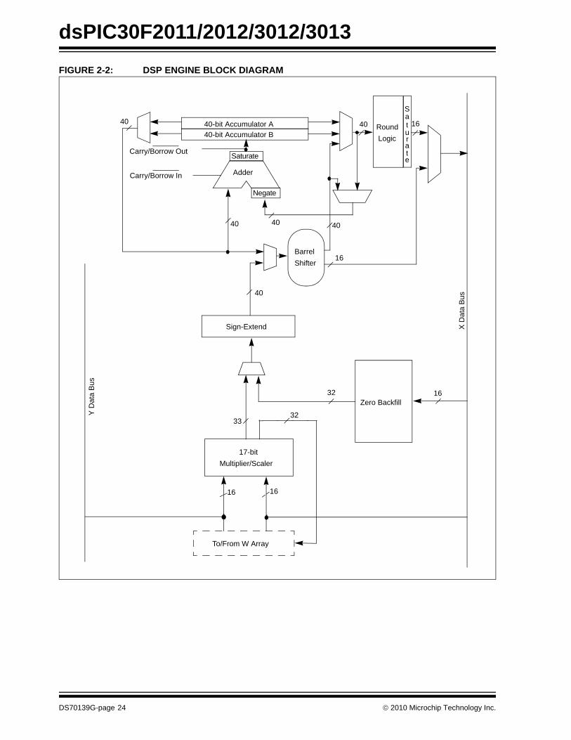
2.4 DSP EngineThe DSP engine consists of a high-speed 17-bit x17-bit multiplier, a barrel shifter and a 40-bitadder/subtracter (with two target accumulators, roundand saturation logic).The DSP engine also has the capability to performinherent accumulator-to-accumulator operations,which require no additional data. These instructions areADD, SUB and NEG.
The dsPIC30F is a single-cycle instruction flowarchitecture, therefore, concurrent operation of theDSP engine with MCU instruction flow is not possible.However, some MCU ALU and DSP engine resourcesmay be used concurrently by the same instruction(e.g., ED, EDAC). See Table 2-2.
The DSP engine has several options selected throughvarious bits in the CPU Core Configuration register(CORCON), which are:
1. Fractional or integer DSP multiply (IF).2. Signed or unsigned DSP multiply (US).3. Conventional or convergent rounding (RND).4. Automatic saturation on/off for ACCA (SATA).5. Automatic saturation on/off for ACCB (SATB).6. Automatic saturation on/off for writes to data
memory (SATDW).7. Accumulator Saturation mode selection
(ACCSAT).
A block diagram of the DSP engine is shown inFigure 2-2.
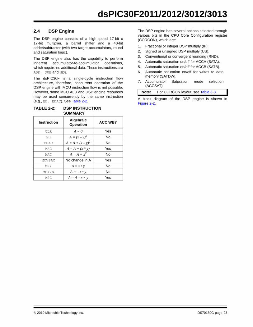
TABLE 2-2: DSP INSTRUCTION SUMMARY
Instruction Algebraic Operation ACC WB?
CLR A = 0 YesED A = (x – y)2 NoEDAC A = A + (x – y)2 NoMAC A = A + (x * y) YesMAC A = A + x2 No
MOVSAC No change in A YesMPY A = x • y No
MPY.N A = – x • y NoMSC A = A – x • y Yes
Note: For CORCON layout, see Table 3-3.
© 2010 Microchip Technology Inc. DS70139G-page 23
dsPIC30F2011/2012/3012/3013
FIGURE 2-2: DSP ENGINE BLOCK DIAGRAMZero Backfill
Sign-Extend
BarrelShifter
40-bit Accumulator A40-bit Accumulator B
RoundLogic
X D
ata
Bus
To/From W Array
Adder
Saturate
Negate
32
3233
16
16 16
16
40 40
40 40
Saturate
Y D
ata
Bus
40
Carry/Borrow Out
Carry/Borrow In
16
40
Multiplier/Scaler17-bit
DS70139G-page 24 © 2010 Microchip Technology Inc.
dsPIC30F2011/2012/3012/3013
2.4.1 MULTIPLIERThe 17 x 17-bit multiplier is capable of signed orunsigned operation and can multiplex its output using ascaler to support either 1.31 fractional (Q31) or 32-bitinteger results. Unsigned operands are zero-extendedinto the 17th bit of the multiplier input value. Signedoperands are sign-extended into the 17th bit of themultiplier input value. The output of the 17 x 17-bitmultiplier/scaler is a 33-bit value which issign-extended to 40 bits. Integer data is inherentlyrepresented as a signed two’s complement value,where the MSB is defined as a sign bit. Generallyspeaking, the range of an N-bit two’s complementinteger is -2N-1 to 2N-1 – 1. For a 16-bit integer, the datarange is -32768 (0x8000) to 32767 (0x7FFF) including‘0’. For a 32-bit integer, the data range is-2,147,483,648 (0x8000 0000) to 2,147,483,645(0x7FFF FFFF).When the multiplier is configured for fractionalmultiplication, the data is represented as a two’scomplement fraction, where the MSB is defined as asign bit and the radix point is implied to lie just after thesign bit (QX format). The range of an N-bit two’scomplement fraction with this implied radix point is -1.0to (1 – 21-N). For a 16-bit fraction, the Q15 data rangeis -1.0 (0x8000) to 0.999969482 (0x7FFF) including ‘0’and has a precision of 3.01518x10⁻⁵. In Fractionalmode, the 16x16 multiply operation generates a 1.31product, which has a precision of 4.65661 x 10⁻¹⁰.
The same multiplier is used to support the MCUmultiply instructions, which include integer 16-bitsigned, unsigned and mixed sign multiplies.
The MUL instruction can be directed to use byte orword-sized operands. Byte operands direct a 16-bitresult. Word operands direct a 32-bit result to thespecified register(s) in the W array.
2.4.2 DATA ACCUMULATORS AND ADDER/SUBTRACTER
The data accumulator consists of a 40-bitadder/subtracter with automatic sign extension logic. Itcan select one of two accumulators (A or B) as itspre-accumulation source and post-accumulationdestination. For the ADD and LAC instructions, the datato be accumulated or loaded can be optionally scaledthrough the barrel shifter prior to accumulation.
2.4.2.1 Adder/Subtracter, Overflow and Saturation
The adder/subtracter is a 40-bit adder with an optionalzero input into one side and either true or complementdata into the other input. In the case of addition, thecarry/borrow input is active high and the other input istrue data (not complemented), whereas in the case ofsubtraction, the carry/borrow input is active low and theother input is complemented. The adder/subtractergenerates overflow status bits SA/SB and OA/OB,which are latched and reflected in the STATUS register:
• Overflow from bit 39: This is a catastrophic overflow in which the sign of the accumulator is destroyed.
• Overflow into guard bits 32 through 39: This is a recoverable overflow. This bit is set whenever all the guard bits are not identical to each other.
The adder has an additional saturation block whichcontrols accumulator data saturation if selected. It usesthe result of the adder, the overflow Status bitsdescribed above, and the mode control bits SATA/B(CORCON<7:6>) and ACCSAT (CORCON<4>) todetermine when and to what value to saturate.
Six STATUS register bits have been provided tosupport saturation and overflow. They are:
• OA: ACCA overflowed into guard bits • OB: ACCB overflowed into guard bits• SA: ACCA saturated (bit 31 overflow and
saturation)orACCA overflowed into guard bits and saturated (bit 39 overflow and saturation)
• SB: ACCB saturated (bit 31 overflow and saturation)orACCB overflowed into guard bits and saturated (bit 39 overflow and saturation)
• OAB: Logical OR of OA and OB• SAB: Logical OR of SA and SB
The OA and OB bits are modified each time datapasses through the adder/subtracter. When set, theyindicate that the most recent operation has overflowedinto the accumulator guard bits (bits 32 through 39).The OA and OB bits can also optionally generate anarithmetic warning trap when set and thecorresponding overflow trap flag enable bit (OVATE,OVBTE) in the INTCON1 register (refer to Section 8.0“Interrupts”) is set. This allows the user to takeimmediate action, for example, to correct system gain.
© 2010 Microchip Technology Inc. DS70139G-page 25
dsPIC30F2011/2012/3012/3013
The SA and SB bits are modified each time datapasses through the adder/subtracter but can only becleared by the user. When set, they indicate that theaccumulator has overflowed its maximum range (bit 31for 32-bit saturation or bit 39 for 40-bit saturation) andwill be saturated if saturation is enabled. When satura-tion is not enabled, SA and SB default to bit 39 overflowand thus indicate that a catastrophic overflow hasoccurred. If the COVTE bit in the INTCON1 register isset, SA and SB bits generate an arithmetic warning trapwhen saturation is disabled.The overflow and saturation Status bits can optionallybe viewed in the STATUS register (SR) as the logicalOR of OA and OB (in bit OAB) and the logical OR of SAand SB (in bit SAB). This allows programmers to checkone bit in the STATUS register to determine if eitheraccumulator has overflowed, or one bit to determine ifeither accumulator has saturated. This would be usefulfor complex number arithmetic which typically usesboth the accumulators.
The device supports three saturation and overflowmodes:
1. Bit 39 Overflow and Saturation:When bit 39 overflow and saturation occurs, thesaturation logic loads the maximally positive 9.31(0x7FFFFFFFFF) or maximally negative 9.31value (0x8000000000) into the targetaccumulator. The SA or SB bit is set and remainsset until cleared by the user. This is referred to as‘super saturation’ and provides protection againsterroneous data or unexpected algorithmproblems (e.g., gain calculations).
2. Bit 31 Overflow and Saturation:When bit 31 overflow and saturation occurs, thesaturation logic then loads the maximally posi-tive 1.31 value (0x007FFFFFFF) or maximallynegative 1.31 value (0x0080000000) into thetarget accumulator. The SA or SB bit is set andremains set until cleared by the user. When thisSaturation mode is in effect, the guard bits arenot used, so the OA, OB or OAB bits are neverset.
3. Bit 39 Catastrophic Overflow:The bit 39 overflow Status bit from the adder isused to set the SA or SB bit which remains setuntil cleared by the user. No saturation operationis performed and the accumulator is allowed tooverflow (destroying its sign). If the COVTE bit inthe INTCON1 register is set, a catastrophicoverflow can initiate a trap exception.
2.4.2.2 Accumulator ‘Write-Back’The MAC class of instructions (with the exception ofMPY, MPY.N, ED and EDAC) can optionally write arounded version of the high word (bits 31 through 16)of the accumulator that is not targeted by the instructioninto data space memory. The write is performed acrossthe X bus into combined X and Y address space. Thefollowing addressing modes are supported:
1. W13, Register Direct:The rounded contents of the non-targetaccumulator are written into W13 as a 1.15fraction.
2. [W13]+ = 2, Register Indirect withPost-Increment:The rounded contents of the non-targetaccumulator are written into the address pointedto by W13 as a 1.15 fraction. W13 is thenincremented by 2 (for a word write).
2.4.2.3 Round LogicThe round logic is a combinational block whichperforms a conventional (biased) or convergent(unbiased) round function during an accumulator write(store). The Round mode is determined by the state ofthe RND bit in the CORCON register. It generates a16-bit, 1.15 data value, which is passed to the dataspace write saturation logic. If rounding is not indicatedby the instruction, a truncated 1.15 data value is storedand the least significant word (lsw) is simply discarded.
Conventional rounding takes bit 15 of the accumulator,zero-extends it and adds it to the ACCxH word (bits 16through 31 of the accumulator). If the ACCxL word(bits 0 through 15 of the accumulator) is between0x8000 and 0xFFFF (0x8000 included), ACCxH isincremented. If ACCxL is between 0x0000 and 0x7FFF,ACCxH is left unchanged. A consequence of thisalgorithm is that over a succession of random roundingoperations, the value tends to be biased slightlypositive.
Convergent (or unbiased) rounding operates in thesame manner as conventional rounding, except whenACCxL equals 0x8000. If this is the case, the LSb(bit 16 of the accumulator) of ACCxH is examined. If itis ‘1’, ACCxH is incremented. If it is ‘0’, ACCxH is notmodified. Assuming that bit 16 is effectively random innature, this scheme will remove any rounding bias thatmay accumulate.
The SAC and SAC.R instructions store either atruncated (SAC) or rounded (SAC.R) version of thecontents of the target accumulator to data memory viathe X bus (subject to data saturation, seeSection 2.4.2.4 “Data Space Write Saturation”).Note that for the MAC class of instructions, theaccumulator write-back operation functions in thesame manner, addressing combined MCU (X and Y)data space though the X bus. For this class ofinstructions, the data is always subject to rounding.
DS70139G-page 26 © 2010 Microchip Technology Inc.
dsPIC30F2011/2012/3012/3013
2.4.2.4 Data Space Write SaturationIn addition to adder/subtracter saturation, writes to dataspace may also be saturated but without affecting thecontents of the source accumulator. The data spacewrite saturation logic block accepts a 16-bit, 1.15fractional value from the round logic block as its input,together with overflow status from the original source(accumulator) and the 16-bit round adder. These arecombined and used to select the appropriate 1.15fractional value as output to write to data spacememory.If the SATDW bit in the CORCON register is set, data(after rounding or truncation) is tested for overflow andadjusted accordingly. For input data greater than0x007FFF, data written to memory is forced to themaximum positive 1.15 value, 0x7FFF. For input dataless than 0xFF8000, data written to memory is forcedto the maximum negative 1.15 value, 0x8000. The MSbof the source (bit 39) is used to determine the sign ofthe operand being tested.
If the SATDW bit in the CORCON register is not set, theinput data is always passed through unmodified underall conditions.
2.4.3 BARREL SHIFTERThe barrel shifter is capable of performing up to 16-bitarithmetic or logic right shifts, or up to 16-bit left shiftsin a single cycle. The source can be either of the twoDSP accumulators, or the X bus (to support multi-bitshifts of register or memory data).
The shifter requires a signed binary value to determineboth the magnitude (number of bits) and direction of theshift operation. A positive value shifts the operand right.A negative value shifts the operand left. A value of ‘0’does not modify the operand.
The barrel shifter is 40 bits wide, thereby obtaining a40-bit result for DSP shift operations and a 16-bit resultfor MCU shift operations. Data from the X bus ispresented to the barrel shifter between bit positions 16to 31 for right shifts, and bit positions 0 to 16 for leftshifts.
© 2010 Microchip Technology Inc. DS70139G-page 27

dsPIC30F2011/2012/3012/3013
NOTES:DS70139G-page 28 © 2010 Microchip Technology Inc.
dsPIC30F2011/2012/3012/3013
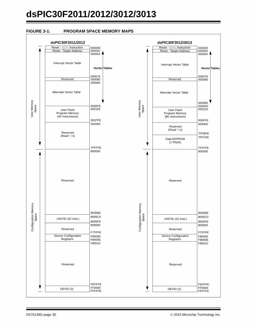
3.0 MEMORY ORGANIZATION
3.1 Program Address SpaceThe program address space is 4M instruction words.The program space memory maps for thedsPIC30F2011/2012/3012/3013 devices is shown inFigure 3-1.
Program memory is addressable by a 24-bit value fromeither the 23-bit PC, table instruction Effective Address(EA), or data space EA, when program space ismapped into data space as defined by Table 3-1. Notethat the program space address is incremented by twobetween successive program words in order to providecompatibility with data space addressing.
User program space access is restricted to the lower4M instruction word address range (0x000000 to0x7FFFFE) for all accesses other than TBLRD/TBLWT,which uses TBLPAG<7> to determine user or configu-ration space access. In Table 3-1, Program SpaceAddress Construction, bit 23 allows access to theDevice ID, the User ID and the Configuration bits.Otherwise, bit 23 is always clear.
Note: This data sheet summarizes features ofthis group of dsPIC30F devices and is notintended to be a complete referencesource. For more information on the CPU,peripherals, register descriptions andgeneral device functionality, refer to the“dsPIC30F Family Reference Manual”(DS70046). For more information on thedevice instruction set and programming,refer to the “16-bit MCU and DSCProgrammer’s Reference Manual”(DS70157).
© 2010 Microchip Technology Inc. DS70139G-page 29
dsPIC30F2011/2012/3012/3013
FIGURE 3-1: PROGRAM SPACE MEMORY MAPSReset - Target Address
Use
r Mem
ory
Spac
e
000000
00007E
000002
000080
Device Configuration
User FlashProgram Memory
002000001FFE
Con
figur
atio
n M
emor
ySp
ace
(4K instructions)
800000
F80000Registers F8000E
F80010
DEVID (2)FEFFFEFF0000FFFFFE
ReservedF7FFFE
Reserved(Read ‘0’s)
8005FE800600
UNITID (32 instr.)
Vector Tables
8005BE8005C0
Reset - GOTO Instruction
000004
Reserved
7FFFFE
Reserved
0001000000FE
000084
Alternate Vector Table
Reserved
Interrupt Vector Table
Reset - Target Address
Use
r Mem
ory
Spac
e
000000
00007E
000002
000080
Device Configuration
User FlashProgram Memory
004000003FFE
Con
figur
atio
n M
emor
ySp
ace
Data EEPROM
(8K instructions)
(1 Kbyte)
800000
F80000Registers F8000E
F80010
DEVID (2)FEFFFEFF0000FFFFFE
ReservedF7FFFE
Reserved
7FFC007FFBFE
(Read ‘0’s)
8005FE800600
UNITID (32 instr.)
Vector Tables
8005BE8005C0
Reset - GOTO Instruction
000004
Reserved
7FFFFE
Reserved
0001000000FE000084
Alternate Vector Table
Reserved
Interrupt Vector Table
dsPIC30F2011/2012 dsPIC30F3012/3013
DS70139G-page 30 © 2010 Microchip Technology Inc.
dsPIC30F2011/2012/3012/3013
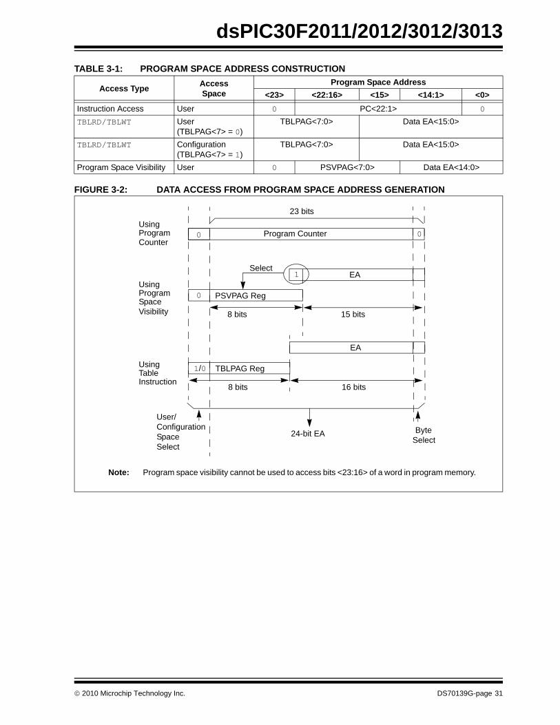
TABLE 3-1: PROGRAM SPACE ADDRESS CONSTRUCTIONFIGURE 3-2: DATA ACCESS FROM PROGRAM SPACE ADDRESS GENERATION
Access Type AccessSpace
Program Space Address<23> <22:16> <15> <14:1> <0>
Instruction Access User 0 PC<22:1> 0
TBLRD/TBLWT User (TBLPAG<7> = 0)
TBLPAG<7:0> Data EA<15:0>
TBLRD/TBLWT Configuration (TBLPAG<7> = 1)
TBLPAG<7:0> Data EA<15:0>
Program Space Visibility User 0 PSVPAG<7:0> Data EA<14:0>
0Program Counter
23 bits
1
PSVPAG Reg
8 bits
EA
15 bits
Program
Using
Select
TBLPAG Reg
8 bits
EA
16 bits
Using
Byte24-bit EA
0
0
1/0
Select
User/Configuration
TableInstruction
ProgramSpace
Counter
Using
SpaceSelect
Visibility
Note: Program space visibility cannot be used to access bits <23:16> of a word in program memory.
© 2010 Microchip Technology Inc. DS70139G-page 31
dsPIC30F2011/2012/3012/3013
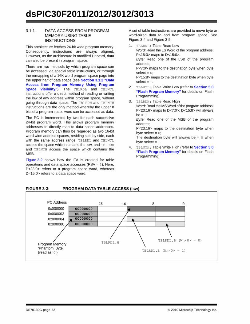
3.1.1 DATA ACCESS FROM PROGRAMMEMORY USING TABLE INSTRUCTIONS
This architecture fetches 24-bit wide program memory.Consequently, instructions are always aligned.However, as the architecture is modified Harvard, datacan also be present in program space.
There are two methods by which program space canbe accessed: via special table instructions, or throughthe remapping of a 16K word program space page intothe upper half of data space (see Section 3.1.2 “DataAccess from Program Memory Using ProgramSpace Visibility”). The TBLRDL and TBLWTLinstructions offer a direct method of reading or writingthe lsw of any address within program space, withoutgoing through data space. The TBLRDH and TBLWTHinstructions are the only method whereby the upper 8bits of a program space word can be accessed as data.
The PC is incremented by two for each successive24-bit program word. This allows program memoryaddresses to directly map to data space addresses.Program memory can thus be regarded as two 16-bitword wide address spaces, residing side by side, eachwith the same address range. TBLRDL and TBLWTLaccess the space which contains the lsw, and TBLRDHand TBLWTH access the space which contains theMSB.
Figure 3-2 shows how the EA is created for tableoperations and data space accesses (PSV = 1). Here,P<23:0> refers to a program space word, whereasD<15:0> refers to a data space word.
A set of table instructions are provided to move byte orword-sized data to and from program space. SeeFigure 3-4 and Figure 3-5.
1. TBLRDL: Table Read LowWord: Read the LS Word of the program address;P<15:0> maps to D<15:0>.Byte: Read one of the LSB of the programaddress;P<7:0> maps to the destination byte when byteselect = 0;P<15:8> maps to the destination byte when byteselect = 1.
2. TBLWTL: Table Write Low (refer to Section 5.0“Flash Program Memory” for details on FlashProgramming)
3. TBLRDH: Table Read HighWord: Read the MS Word of the program address;P<23:16> maps to D<7:0>; D<15:8> will alwaysbe = 0.Byte: Read one of the MSB of the programaddress;P<23:16> maps to the destination byte whenbyte select = 0;The destination byte will always be = 0 whenbyte select = 1.
4. TBLWTH: Table Write High (refer to Section 5.0“Flash Program Memory” for details on FlashProgramming)
FIGURE 3-3: PROGRAM DATA TABLE ACCESS (lsw)
0816PC Address
0x0000000x0000020x0000040x000006
230000000000000000
0000000000000000
Program Memory‘Phantom’ Byte(read as ‘0’)
TBLRDL.W
TBLRDL.B (Wn<0> = 1)
TBLRDL.B (Wn<0> = 0)
DS70139G-page 32 © 2010 Microchip Technology Inc.
dsPIC30F2011/2012/3012/3013
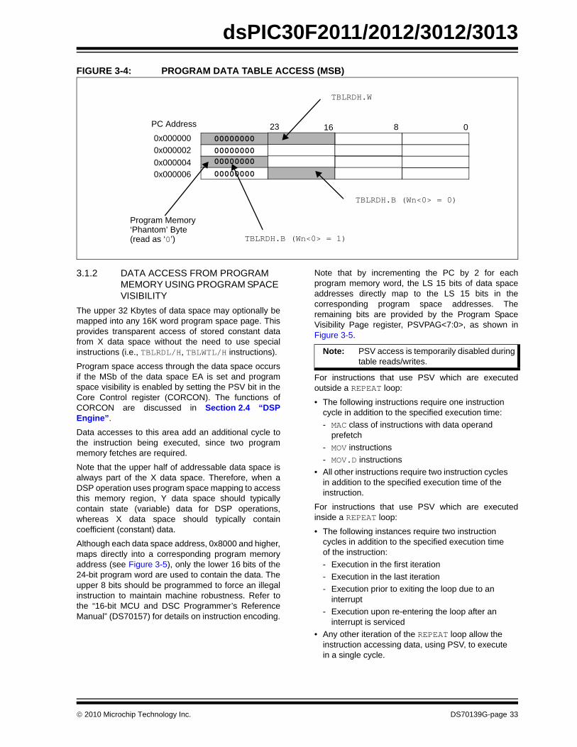
FIGURE 3-4: PROGRAM DATA TABLE ACCESS (MSB)3.1.2 DATA ACCESS FROM PROGRAM MEMORY USING PROGRAM SPACE VISIBILITY
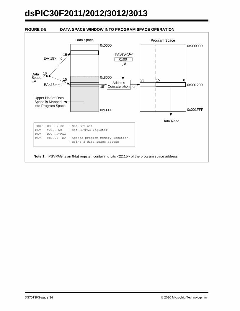
The upper 32 Kbytes of data space may optionally bemapped into any 16K word program space page. Thisprovides transparent access of stored constant datafrom X data space without the need to use specialinstructions (i.e., TBLRDL/H, TBLWTL/H instructions).
Program space access through the data space occursif the MSb of the data space EA is set and programspace visibility is enabled by setting the PSV bit in theCore Control register (CORCON). The functions ofCORCON are discussed in Section 2.4 “DSPEngine”.
Data accesses to this area add an additional cycle tothe instruction being executed, since two programmemory fetches are required.
Note that the upper half of addressable data space isalways part of the X data space. Therefore, when aDSP operation uses program space mapping to accessthis memory region, Y data space should typicallycontain state (variable) data for DSP operations,whereas X data space should typically containcoefficient (constant) data.
Although each data space address, 0x8000 and higher,maps directly into a corresponding program memoryaddress (see Figure 3-5), only the lower 16 bits of the24-bit program word are used to contain the data. Theupper 8 bits should be programmed to force an illegalinstruction to maintain machine robustness. Refer tothe “16-bit MCU and DSC Programmer’s ReferenceManual” (DS70157) for details on instruction encoding.
Note that by incrementing the PC by 2 for eachprogram memory word, the LS 15 bits of data spaceaddresses directly map to the LS 15 bits in thecorresponding program space addresses. Theremaining bits are provided by the Program SpaceVisibility Page register, PSVPAG<7:0>, as shown inFigure 3-5.
For instructions that use PSV which are executedoutside a REPEAT loop:
• The following instructions require one instruction cycle in addition to the specified execution time: - MAC class of instructions with data operand
prefetch- MOV instructions- MOV.D instructions
• All other instructions require two instruction cycles in addition to the specified execution time of the instruction.
For instructions that use PSV which are executedinside a REPEAT loop:
• The following instances require two instruction cycles in addition to the specified execution time of the instruction:- Execution in the first iteration- Execution in the last iteration- Execution prior to exiting the loop due to an
interrupt- Execution upon re-entering the loop after an
interrupt is serviced• Any other iteration of the REPEAT loop allow the
instruction accessing data, using PSV, to execute in a single cycle.
0816PC Address
0x0000000x0000020x0000040x000006
230000000000000000
0000000000000000
Program Memory‘Phantom’ Byte(read as ‘0’)
TBLRDH.W
TBLRDH.B (Wn<0> = 1)
TBLRDH.B (Wn<0> = 0)
Note: PSV access is temporarily disabled duringtable reads/writes.
© 2010 Microchip Technology Inc. DS70139G-page 33
dsPIC30F2011/2012/3012/3013
FIGURE 3-5: DATA SPACE WINDOW INTO PROGRAM SPACE OPERATION23 15 0
PSVPAG(1)15
15
EA<15> = 0
EA<15> = 1
16DataSpaceEA
Data Space Program Space
8
15 23
0x0000
0x8000
0xFFFF
0x00
0x001FFF
Data Read
Upper Half of Data Space is Mapped into Program Space
0x001200AddressConcatenation
BSET CORCON,#2 ; Set PSV bitMOV #0x0, W0 ; Set PSVPAG registerMOV W0, PSVPAGMOV 0x9200, W0 ; Access program memory location
; using a data space access
Note 1: PSVPAG is an 8-bit register, containing bits <22:15> of the program space address.
0x000000
DS70139G-page 34 © 2010 Microchip Technology Inc.
dsPIC30F2011/2012/3012/3013
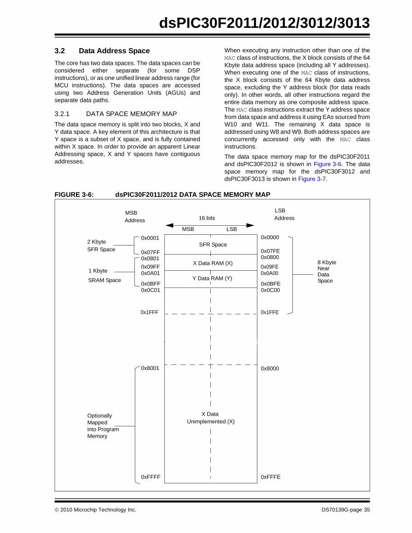
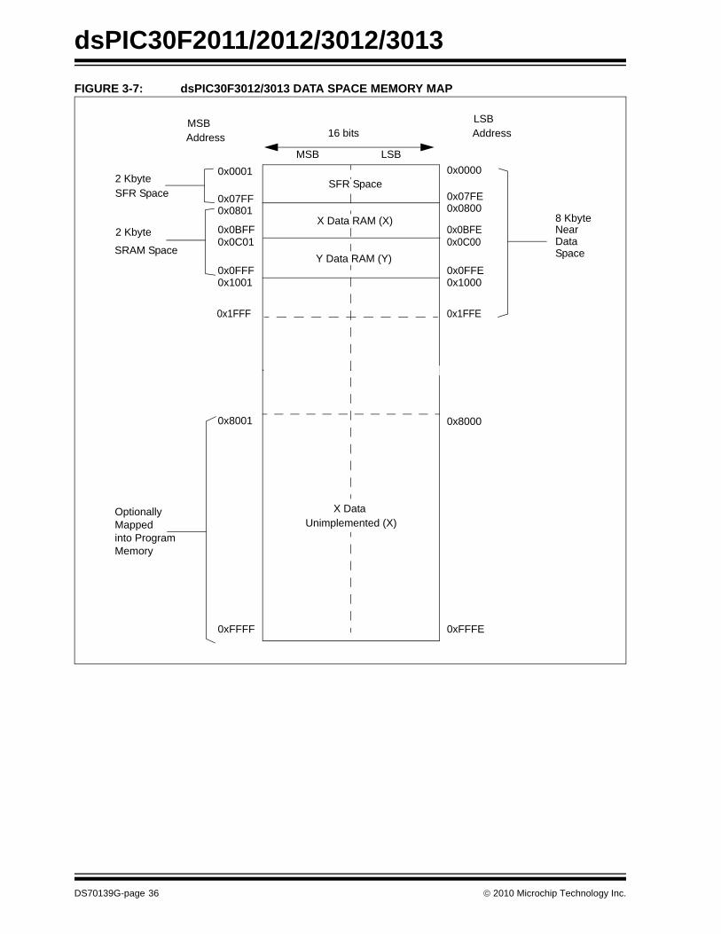
3.2 Data Address SpaceThe core has two data spaces. The data spaces can beconsidered either separate (for some DSPinstructions), or as one unified linear address range (forMCU instructions). The data spaces are accessedusing two Address Generation Units (AGUs) andseparate data paths.3.2.1 DATA SPACE MEMORY MAPThe data space memory is split into two blocks, X andY data space. A key element of this architecture is thatY space is a subset of X space, and is fully containedwithin X space. In order to provide an apparent LinearAddressing space, X and Y spaces have contiguousaddresses.
When executing any instruction other than one of theMAC class of instructions, the X block consists of the 64Kbyte data address space (including all Y addresses).When executing one of the MAC class of instructions,the X block consists of the 64 Kbyte data addressspace, excluding the Y address block (for data readsonly). In other words, all other instructions regard theentire data memory as one composite address space.The MAC class instructions extract the Y address spacefrom data space and address it using EAs sourced fromW10 and W11. The remaining X data space isaddressed using W8 and W9. Both address spaces areconcurrently accessed only with the MAC classinstructions.
The data space memory map for the dsPIC30F2011and dsPIC30F2012 is shown in Figure 3-6. The dataspace memory map for the dsPIC30F3012 anddsPIC30F3013 is shown in Figure 3-7.
FIGURE 3-6: dsPIC30F2011/2012 DATA SPACE MEMORY MAP
0x0000
0x07FE
0x09FE
0xFFFE
LSBAddress16 bits
LSBMSB
MSBAddress
0x0001
0x07FF
0x09FF
0xFFFF
0x8001 0x8000
OptionallyMappedinto ProgramMemory
0x0BFF 0x0BFE0x0C000x0C01
0x0801 0x0800
0x0A01 0x0A00NearData
0x1FFE 0x1FFF
2 KbyteSFR Space
1 Kbyte
SRAM Space
8 Kbyte
Space
X Data Unimplemented (X)
SFR Space
X Data RAM (X)
Y Data RAM (Y)
© 2010 Microchip Technology Inc. DS70139G-page 35
dsPIC30F2011/2012/3012/3013
FIGURE 3-7: dsPIC30F3012/3013 DATA SPACE MEMORY MAP0x0000
0x07FE
0x0BFE
0xFFFE
LSBAddress16 bits
LSBMSB
MSBAddress
0x0001
0x07FF
0x0BFF
0xFFFF
0x8001 0x8000
OptionallyMappedinto ProgramMemory
0x0FFF 0x0FFE0x10000x1001
0x0801 0x0800
0x0C01 0x0C00NearData
0x1FFE 0x1FFF
2 KbyteSFR Space
2 Kbyte
SRAM Space
8 Kbyte
Space
X Data Unimplemented (X)
SFR Space
X Data RAM (X)
Y Data RAM (Y)
DS70139G-page 36 © 2010 Microchip Technology Inc.
dsPIC30F2011/2012/3012/3013
FIGURE 3-8: DATA SPACE FOR MCU AND DSP (MAC CLASS) INSTRUCTIONS EXAMPLESFR SPACE
(Y SPACE)
X S
PAC
E
SFR SPACE
UNUSED
X S
PAC
EX
SPA
CE
Y SPACE
UNUSED
UNUSED
Non-MAC Class Ops (Read/Write) MAC Class Ops (Read)
Indirect EA using any W Indirect EA using W8, W9 Indirect EA using W10, W11
MAC Class Ops (Write)
© 2010 Microchip Technology Inc. DS70139G-page 37
dsPIC30F2011/2012/3012/3013
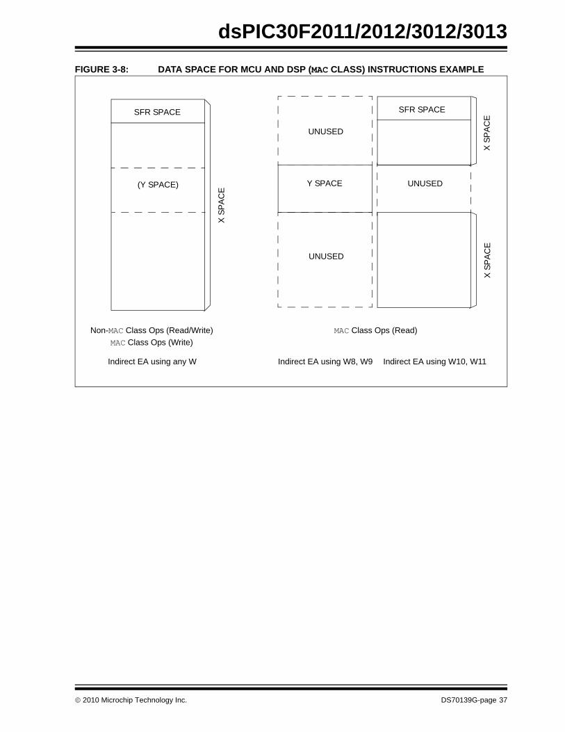
3.2.2 DATA SPACESThe X data space is used by all instructions and sup-ports all addressing modes. There are separate readand write data buses. The X read data bus is the returndata path for all instructions that view data space ascombined X and Y address space. It is also the Xaddress space data path for the dual operand readinstructions (MAC class). The X write data bus is theonly write path to data space for all instructions.The X data space also supports Modulo Addressing forall instructions, subject to Addressing mode restric-tions. Bit-Reversed Addressing is only supported forwrites to X data space.
The Y data space is used in concert with the X dataspace by the MAC class of instructions (CLR, ED,EDAC, MAC, MOVSAC, MPY, MPY.N and MSC) toprovide two concurrent data read paths. No writesoccur across the Y bus. This class of instructionsdedicates two W register pointers, W10 and W11, toalways address Y data space, independent of X dataspace, whereas W8 and W9 always address X dataspace. Note that during accumulator write back, thedata address space is considered a combination of Xand Y data spaces, so the write occurs across the Xbus. Consequently, the write can be to any address inthe entire data space.
The Y data space can only be used for the dataprefetch operation associated with the MAC class ofinstructions. It also supports Modulo Addressing forautomated circular buffers. Of course, all otherinstructions can access the Y data address spacethrough the X data path as part of the composite linearspace.
The boundary between the X and Y data spaces isdefined as shown in Figure 3-7 and is not userprogrammable. Should an EA point to data outside itsown assigned address space, or to a location outsidephysical memory, an all zero word/byte is returned. Forexample, although Y address space is visible by allnon-MAC instructions using any addressing mode, anattempt by a MAC instruction to fetch data from thatspace using W8 or W9 (X space pointers)returns 0x0000.
TABLE 3-2: EFFECT OF INVALID MEMORY ACCESSES
All Effective Addresses are 16 bits wide and point tobytes within the data space. Therefore, the data spaceaddress range is 64 Kbytes or 32K words.
3.2.3 DATA SPACE WIDTHThe core data width is 16 bits. All internal registers areorganized as 16-bit wide words. Data space memory isorganized in byte addressable, 16-bit wide blocks.
3.2.4 DATA ALIGNMENTTo help maintain backward compatibility withPIC® MCU devices and improve data space memoryusage efficiency, the dsPIC30F instruction set supportsboth word and byte operations. Data is aligned in datamemory and registers as words, but all data space EAsresolve to bytes. Data byte reads read the completeword that contains the byte, using the LSb of any EA todetermine which byte to select. The selected byte isplaced onto the LSB of the X data path (no byteaccesses are possible from the Y data path as the MACclass of instruction can only fetch words). That is, datamemory and registers are organized as two parallelbyte wide entities with shared (word) address decodebut separate write lines. Data byte writes only write tothe corresponding side of the array or register whichmatches the byte address.
As a consequence of this byte accessibility, all EffectiveAddress calculations (including those generated by theDSP operations which are restricted to word-sizeddata) are internally scaled to step through word-alignedmemory. For example, the core would recognize thatPost-Modified Register Indirect Addressing mode[Ws++] results in a value of Ws + 1 for byte operationsand Ws + 2 for word operations.
All word accesses must be aligned to an even address.Misaligned word data fetches are not supported, socare should be taken when mixing byte and wordoperations, or translating from 8-bit MCU code. Shoulda misaligned read or write be attempted, an addresserror trap is generated. If the error occurred on a read,the instruction underway is completed, whereas if itoccurred on a write, the instruction is executed, but thewrite does not occur. In either case, a trap is thenexecuted, allowing the system and/or user to examinethe machine state prior to execution of the addressfault.
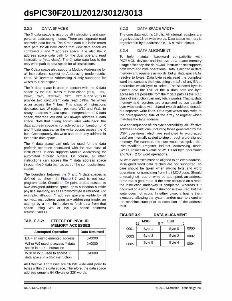
FIGURE 3-9: DATA ALIGNMENT
Attempted Operation Data Returned
EA = an unimplemented address 0x0000W8 or W9 used to access Y data space in a MAC instruction
0x0000
W10 or W11 used to access X data space in a MAC instruction
0x0000
15 8 7 00001
0003
0005
0000
0002
0004
Byte 1 Byte 0
Byte 3 Byte 2
Byte 5 Byte 4
LSBMSB
DS70139G-page 38 © 2010 Microchip Technology Inc.
dsPIC30F2011/2012/3012/3013
All byte loads into any W register are loaded into theLSB. The MSB is not modified.A Sign-Extend (SE) instruction is provided to allowusers to translate 8-bit signed data to 16-bit signedvalues. Alternatively, for 16-bit unsigned data, userscan clear the MSB of any W register by executing aZero-Extend (ZE) instruction on the appropriateaddress.
Although most instructions are capable of operating onword or byte data sizes, it should be noted that someinstructions, including the DSP instructions, operateonly on words.
3.2.5 NEAR DATA SPACEAn 8 Kbyte near data space is reserved in X addressmemory space between 0x0000 and 0x1FFF, which isdirectly addressable via a 13-bit absolute address fieldwithin all memory direct instructions. The remaining Xaddress space and all of the Y address space isaddressable indirectly. Additionally, the whole of X dataspace is addressable using MOV instructions, whichsupport memory direct addressing with a 16-bitaddress field.
3.2.6 SOFTWARE STACK
The dsPIC DSC devices contain a software stack. W15is used as the Stack Pointer.
The Stack Pointer always points to the first availablefree word and grows from lower addresses towardshigher addresses. It pre-decrements for stack popsand post-increments for stack pushes, as shown inFigure 3-10. Note that for a PC push during any CALLinstruction, the MSB of the PC is zero-extended beforethe push, ensuring that the MSB is always clear.
FIGURE 3-10: CALL STACK FRAME
There is a Stack Pointer Limit register (SPLIM)associated with the Stack Pointer. SPLIM isuninitialized at Reset. As is the case for the StackPointer, SPLIM<0> is forced to ‘0’ because all stackoperations must be word aligned. Whenever anEffective Address (EA) is generated using W15 as asource or destination pointer, the address thusgenerated is compared with the value in SPLIM. If thecontents of the Stack Pointer (W15) and the SPLIM reg-ister are equal, and a push operation is performed, astack error trap does not occur. The stack error trapoccurs on a subsequent push operation. Thus, forexample, if it is desirable to cause a stack error trapwhen the stack grows beyond address 0x2000 in RAM,initialize the SPLIM with the value, 0x1FFE.
Similarly, a Stack Pointer underflow (stack error) trap isgenerated when the Stack Pointer address is found tobe less than 0x0800, thus preventing the stack frominterfering with the Special Function Register (SFR)space.
A write to the SPLIM register should not be immediatelyfollowed by an indirect read operation using W15.
Note: A PC push during exception processingconcatenates the SRL register to the MSBof the PC prior to the push.
<Free Word>
PC<15:0>000000000
015
W15 (before CALL)
W15 (after CALL)
Stac
k G
row
s To
war
dsH
ighe
r Add
ress
0x0000
PC<22:16>
POP : [--W15]PUSH : [W15++]
© 2010 Microchip Technology Inc. DS70139G-page 39
dsPIC30F2011/2012/3012/3013
DS
70139G-page 40
© 2010 M
icrochip Technology Inc.
3 Bit 2 Bit 1 Bit 0 Reset State
0000 0000 0000 0000
0000 0000 0000 0000
0000 0000 0000 0000
0000 0000 0000 0000
0000 0000 0000 0000
0000 0000 0000 0000
0000 0000 0000 0000
0000 0000 0000 0000
0000 0000 0000 0000
0000 0000 0000 0000
0000 0000 0000 0000
0000 0000 0000 0000
0000 0000 0000 0000
0000 0000 0000 0000
0000 0000 0000 0000
0000 1000 0000 0000
0000 0000 0000 0000
0000 0000 0000 0000
0000 0000 0000 0000
0000 0000 0000 0000
0000 0000 0000 0000
0000 0000 0000 0000
0000 0000 0000 0000
0000 0000 0000 0000
0000 0000 0000 0000
0000 0000 0000 0000
0000 0000 0000 0000
uuuu uuuu uuuu uuuu
uuuu uuuu uuuu uuuu
0 uuuu uuuu uuuu uuu0
TH 0000 0000 0uuu uuuu
0 uuuu uuuu uuuu uuu0
H 0000 0000 0uuu uuuu
OV Z C 0000 0000 0000 0000
TABLE 3-3: CORE REGISTER MAP
SFR Name Address(Home) Bit 15 Bit 14 Bit 13 Bit 12 Bit 11 Bit 10 Bit 9 Bit 8 Bit 7 Bit 6 Bit 5 Bit 4 Bit
W0 0000 W0/WREG
W1 0002 W1
W2 0004 W2
W3 0006 W3
W4 0008 W4
W5 000A W5
W6 000C W6
W7 000E W7
W8 0010 W8
W9 0012 W9
W10 0014 W10
W11 0016 W11
W12 0018 W12
W13 001A W13
W14 001C W14
W15 001E W15
SPLIM 0020 SPLIM
ACCAL 0022 ACCAL
ACCAH 0024 ACCAH
ACCAU 0026 Sign Extension (ACCA<39>) ACCAU
ACCBL 0028 ACCBL
ACCBH 002A ACCBH
ACCBU 002C Sign Extension (ACCB<39>) ACCBU
PCL 002E PCL
PCH 0030 — — — — — — — — — PCH
TBLPAG 0032 — — — — — — — — TBLPAG
PSVPAG 0034 — — — — — — — — PSVPAG
RCOUNT 0036 RCOUNT
DCOUNT 0038 DCOUNT
DOSTARTL 003A DOSTARTL
DOSTARTH 003C — — — — — — — — — DOSTAR
DOENDL 003E DOENDL
DOENDH 0040 — — — — — — — — — DOEND
SR 0042 OA OB SA SB OAB SAB DA DC IPL2 IPL1 IPL0 RA N
Legend: u = uninitialized bit; — = unimplemented bit, read as ‘0’Note: Refer to the “dsPIC30F Family Reference Manual” (DS70046) for descriptions of register bit fields.
© 2010 M
icrochip Technology Inc.D
S70139G
-page 41
dsPIC30F2011/2012/3012/3013
CO PSV RND IF 0000 0000 0010 0000
MO XWM<3:0> 0000 0000 0000 0000
XM 0 uuuu uuuu uuuu uuu0
XM 1 uuuu uuuu uuuu uuu1
YM 0 uuuu uuuu uuuu uuu0
YM 1 uuuu uuuu uuuu uuu1
XB uuuu uuuu uuuu uuuu
DIS 0000 0000 0000 0000
TA
SF Bit 2 Bit 1 Bit 0 Reset State
Le
RCON 0044 — — — US EDT DL2 DL1 DL0 SATA SATB SATDW ACCSAT IPL3
DCON 0046 XMODEN YMODEN — — BWM<3:0> YWM<3:0>
ODSRT 0048 XS<15:1>
ODEND 004A XE<15:1>
ODSRT 004C YS<15:1>
ODEND 004E YE<15:1>
REV 0050 BREN XB<14:0>
ICNT 0052 — — DISICNT<13:0>
BLE 3-3: CORE REGISTER MAP (CONTINUED)
R Name Address(Home) Bit 15 Bit 14 Bit 13 Bit 12 Bit 11 Bit 10 Bit 9 Bit 8 Bit 7 Bit 6 Bit 5 Bit 4 Bit 3
gend: u = uninitialized bit; — = unimplemented bit, read as ‘0’Note: Refer to the “dsPIC30F Family Reference Manual” (DS70046) for descriptions of register bit fields.

dsPIC30F2011/2012/3012/3013
NOTES:DS70139G-page 42 © 2010 Microchip Technology Inc.
dsPIC30F2011/2012/3012/3013
4.0 ADDRESS GENERATOR UNITS
The dsPIC DSC core contains two independentaddress generator units: the X AGU and Y AGU. The YAGU supports word-sized data reads for the DSP MACclass of instructions only. The dsPIC DSC AGUssupport three types of data addressing:
• Linear Addressing• Modulo (Circular) Addressing• Bit-Reversed Addressing
Linear and Modulo Data Addressing modes can beapplied to data space or program space. Bit-ReversedAddressing is only applicable to data space addresses.
4.1 Instruction Addressing ModesThe addressing modes in Table 4-1 form the basis ofthe addressing modes optimized to support the specificfeatures of individual instructions. The addressingmodes provided in the MAC class of instructions aresomewhat different from those in the other instructiontypes.
4.1.1 FILE REGISTER INSTRUCTIONSMost file register instructions use a 13-bit address field(f) to directly address data present in the first 8192bytes of data memory (near data space). Most fileregister instructions employ a working register, W0,which is denoted as WREG in these instructions. Thedestination is typically either the same file register orWREG (with the exception of the MUL instruction),which writes the result to a register or register pair. TheMOV instruction allows additional flexibility and canaccess the entire data space during file registeroperation.
4.1.2 MCU INSTRUCTIONSThe three-operand MCU instructions are of the form:
Operand 3 = Operand 1 <function> Operand 2
where Operand 1 is always a working register (i.e., theaddressing mode can only be register direct), which isreferred to as Wb. Operand 2 can be a W register,fetched from data memory or a 5-bit literal. The resultlocation can be either a W register or an addresslocation. The following addressing modes aresupported by MCU instructions:
• Register Direct• Register Indirect• Register Indirect Post-modified• Register Indirect Pre-modified• 5-bit or 10-bit Literal
TABLE 4-1: FUNDAMENTAL ADDRESSING MODES SUPPORTED
Note: This data sheet summarizes features ofthis group of dsPIC30F devices and is notintended to be a complete referencesource. For more information on the CPU,peripherals, register descriptions andgeneral device functionality, refer to the“dsPIC30F Family Reference Manual”(DS70046). For more information on thedevice instruction set and programming,refer to the “16-bit MCU and DSCProgrammer’s Reference Manual”(DS70157).
Note: Not all instructions support all theaddressing modes given above. Individualinstructions may support different subsetsof these addressing modes.
Addressing Mode Description
File Register Direct The address of the File register is specified explicitly.Register Direct The contents of a register are accessed directly.Register Indirect The contents of Wn forms the EA.Register Indirect Post-modified The contents of Wn forms the EA. Wn is post-modified (incremented or
decremented) by a constant value.Register Indirect Pre-modified Wn is pre-modified (incremented or decremented) by a signed constant value
to form the EA.Register Indirect with Register Offset The sum of Wn and Wb forms the EA.Register Indirect with Literal Offset The sum of Wn and a literal forms the EA.
© 2010 Microchip Technology Inc. DS70139G-page 43
dsPIC30F2011/2012/3012/3013
4.1.3 MOVE AND ACCUMULATORINSTRUCTIONSMove instructions and the DSP accumulator class ofinstructions provide a greater degree of addressingflexibility than other instructions. In addition to theaddressing modes supported by most MCUinstructions, move and accumulator instructions alsosupport Register Indirect with Register OffsetAddressing mode, also referred to as Register Indexedmode.
In summary, the following addressing modes aresupported by move and accumulator instructions:
• Register Direct• Register Indirect• Register Indirect Post-modified• Register Indirect Pre-modified• Register Indirect with Register Offset (Indexed)• Register Indirect with Literal Offset• 8-bit Literal• 16-bit Literal
4.1.4 MAC INSTRUCTIONSThe dual source operand DSP instructions (CLR, ED,EDAC, MAC, MPY, MPY.N, MOVSAC and MSC), alsoreferred to as MAC instructions, utilize a simplified set ofaddressing modes to allow the user to effectivelymanipulate the data pointers through register indirecttables.
The two source operand prefetch registers must belongto the set {W8, W9, W10, W11}. For data reads, W8and W9 are always directed to the X RAGU. W10 andW11 are always directed to the Y AGU. The effectiveaddresses generated (before and after modification)must, therefore, be valid addresses within X data spacefor W8 and W9 and Y data space for W10 and W11.
In summary, the following addressing modes aresupported by the MAC class of instructions:
• Register Indirect• Register Indirect Post-modified by 2• Register Indirect Post-modified by 4• Register Indirect Post-modified by 6• Register Indirect with Register Offset (Indexed)
4.1.5 OTHER INSTRUCTIONSBesides the various addressing modes outlined above,some instructions use literal constants of various sizes.For example, BRA (branch) instructions use 16-bitsigned literals to specify the branch destination directly,whereas the DISI instruction uses a 14-bit unsignedliteral field. In some instructions, such as ADD Acc, thesource of an operand or result is implied by the opcodeitself. Certain operations, such as NOP, do not have anyoperands.
4.2 Modulo AddressingModulo Addressing is a method of providing anautomated means to support circular data buffers usinghardware. The objective is to remove the need forsoftware to perform data address boundary checkswhen executing tightly looped code, as is typical inmany DSP algorithms.
Modulo Addressing can operate in either data orprogram space (since the data pointer mechanism isessentially the same for both). One circular buffer canbe supported in each of the X (which also provides thepointers into program space) and Y data spaces.Modulo Addressing can operate on any W registerpointer. However, it is not advisable to use W14 or W15for Modulo Addressing since these two registers areused as the Stack Frame Pointer and Stack Pointer,respectively.
In general, any particular circular buffer can only beconfigured to operate in one direction, as there arecertain restrictions on the buffer Start address(for incrementing buffers), or end address(for decrementing buffers) based upon the direction ofthe buffer.
The only exception to the usage restrictions is forbuffers that have a power-of-2 length. As these bufferssatisfy the Start and the end address criteria, they canoperate in a Bidirectional mode (i.e., address boundarychecks are performed on both the lower and upperaddress boundaries).
Note: For the MOV instructions, the addressingmode specified in the instruction can differfor the source and destination EA.However, the 4-bit Wb (register offset)field is shared between both source anddestination (but typically only used byone).
Note: Not all instructions support all theaddressing modes given above. Individualinstructions may support different subsetsof these addressing modes.
Note: Register Indirect with Register Offsetaddressing is only available for W9 (in Xspace) and W11 (in Y space).
DS70139G-page 44 © 2010 Microchip Technology Inc.
dsPIC30F2011/2012/3012/3013
4.2.1 START AND END ADDRESSThe Modulo Addressing scheme requires that astarting and an ending address be specified and loadedinto the 16-bit Modulo Buffer Address registers:XMODSRT, XMODEND, YMODSRT and YMODEND(see Table 3-3).The length of a circular buffer is not directly specified. Itis determined by the difference between thecorresponding Start and end addresses. The maximumpossible length of the circular buffer is 32K words(64 Kbytes).
4.2.2 W ADDRESS REGISTER SELECTION
The Modulo and Bit-Reversed Addressing Controlregister, MODCON<15:0>, contains enable flags aswell as a W register field to specify the W addressregisters. The XWM and YWM fields select whichregisters operate with Modulo Addressing.If XWM = 15, X RAGU and X WAGU ModuloAddressing is disabled. Similarly, if YWM = 15, Y AGUModulo Addressing is disabled.
The X Address Space Pointer W register (XWM), towhich Modulo Addressing is to be applied, is stored inMODCON<3:0> (see Table 3-3). Modulo Addressing isenabled for X data space when XWM is set to any valueother than ‘15’ and the XMODEN bit is set atMODCON<15>.
The Y Address Space Pointer W register (YWM), towhich Modulo Addressing is to be applied, is stored inMODCON<7:4>. Modulo Addressing is enabled for Ydata space when YWM is set to any value otherthan ‘15’ and the YMODEN bit is set atMODCON<14>.
FIGURE 4-1: MODULO ADDRESSING OPERATION EXAMPLE
Note: Y space Modulo Addressing EAcalculations assume word-sized data(LSb of every EA is always clear).
0x1100
0x1163
Start Addr = 0x1100End Addr = 0x1163Length = 0x0032 words
ByteAddress MOV #0x1100,W0
MOV W0,XMODSRT ;set modulo start addressMOV #0x1163,W0MOV W0,MODEND ;set modulo end addressMOV #0x8001,W0MOV W0,MODCON ;enable W1, X AGU for modulo
MOV #0x0000,W0 ;W0 holds buffer fill value
MOV #0x1110,W1 ;point W1 to buffer
DO AGAIN,#0x31 ;fill the 50 buffer locationsMOV W0,[W1++] ;fill the next locationAGAIN: INC W0,W0 ;increment the fill value
© 2010 Microchip Technology Inc. DS70139G-page 45
dsPIC30F2011/2012/3012/3013
4.2.3 MODULO ADDRESSINGAPPLICABILITYModulo Addressing can be applied to the EffectiveAddress (EA) calculation associated with any Wregister. It is important to realize that the addressboundaries check for addresses less than, or greaterthan the upper (for incrementing buffers), and lower (fordecrementing buffers) boundary addresses (not justequal to). Address changes may, therefore, jumpbeyond boundaries and still be adjusted correctly.
4.3 Bit-Reversed AddressingBit-Reversed Addressing is intended to simplify datare-ordering for radix-2 FFT algorithms. It is supportedby the X AGU for data writes only.
The modifier, which may be a constant value or registercontents, is regarded as having its bit order reversed. Theaddress source and destination are kept in normal order.Thus, the only operand requiring reversal is the modifier.
4.3.1 BIT-REVERSED ADDRESSING IMPLEMENTATION
Bit-Reversed Addressing is enabled when:
• BWM (W register selection) in the MODCON reg-ister is any value other than ‘15’ (the stack cannot be accessed using Bit-Reversed Addressing)
and
• The BREN bit is set in the XBREV register
and
• The addressing mode used is Register Indirect with Pre-Increment or Post-Increment.
If the length of a bit-reversed buffer is M = 2N bytes,then the last ‘N’ bits of the data buffer Start addressmust be zeros.
XB<14:0> is the bit-reversed address modifier or ‘pivotpoint’ which is typically a constant. In the case of anFFT computation, its value is equal to half of the FFTdata buffer size.
When enabled, Bit-Reversed Addressing is onlyexecuted for register indirect with pre-increment orpost-increment addressing and word-sized data writes.It does not function for any other addressing mode orfor byte-sized data. Normal addresses are generatedinstead. When Bit-Reversed Addressing is active, theW address pointer is always added to the addressmodifier (XB) and the offset associated with theRegister Indirect Addressing mode is ignored. Inaddition, as word-sized data is a requirement, the LSbof the EA is ignored (and always clear).
If Bit-Reversed Addressing has already been enabledby setting the BREN bit (XBREV<15>), then a write tothe XBREV register should not be immediately followedby an indirect read operation using the W register thathas been designated as the bit-reversed pointer.
Note: The modulo corrected Effective Addressis written back to the register only whenPre-Modify or Post-Modify Addressingmode is used to compute the EA. Whenan address offset (e.g., [W7+W2]) is used,Modulo address correction is performed,but the contents of the register remainunchanged.
Note: All bit-reversed EA calculations assumeword-sized data (LSb of every EA isalways clear). The XB value is scaledaccordingly to generate compatible (byte)addresses.
Note: Modulo Addressing and Bit-ReversedAddressing should not be enabledtogether. In the event that the userattempts to do this, Bit-Reversed Address-ing assumes priority when active for the XWAGU, and X WAGU Modulo Addressingis disabled. However, Modulo Addressingcontinues to function in the X RAGU.
DS70139G-page 46 © 2010 Microchip Technology Inc.
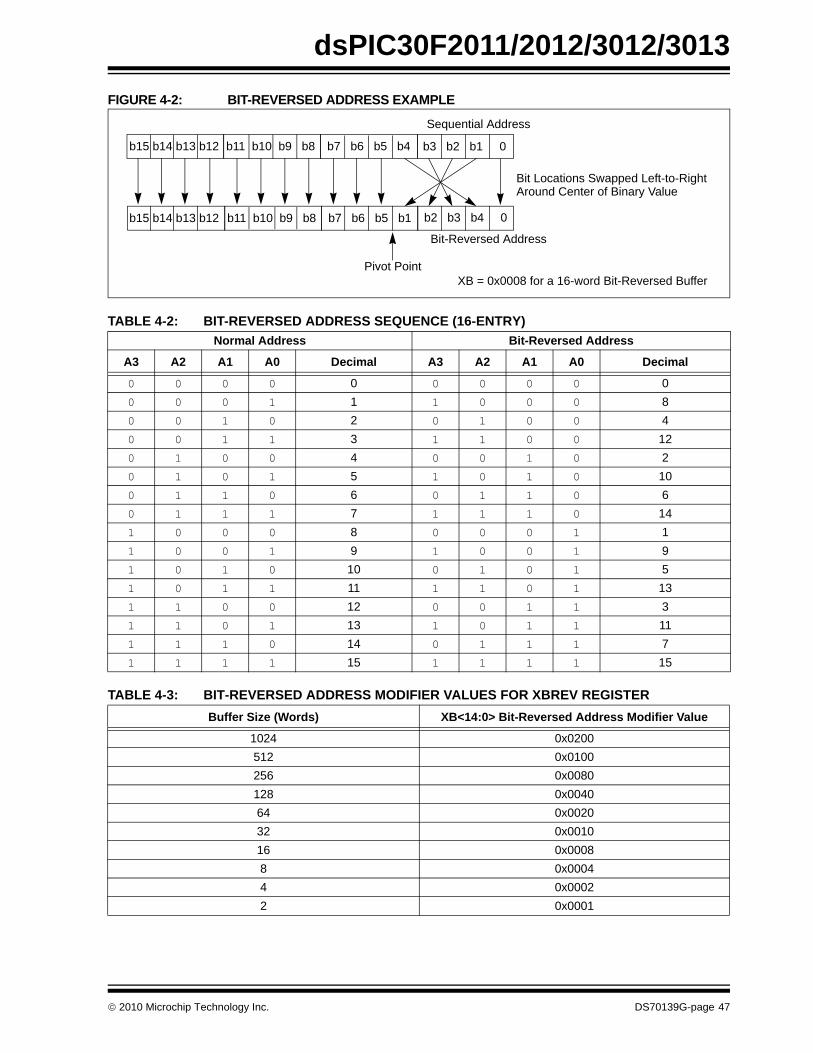
dsPIC30F2011/2012/3012/3013
FIGURE 4-2: BIT-REVERSED ADDRESS EXAMPLETABLE 4-2: BIT-REVERSED ADDRESS SEQUENCE (16-ENTRY)
TABLE 4-3: BIT-REVERSED ADDRESS MODIFIER VALUES FOR XBREV REGISTER
Normal Address Bit-Reversed Address
A3 A2 A1 A0 Decimal A3 A2 A1 A0 Decimal
0 0 0 0 0 0 0 0 0 00 0 0 1 1 1 0 0 0 80 0 1 0 2 0 1 0 0 40 0 1 1 3 1 1 0 0 120 1 0 0 4 0 0 1 0 20 1 0 1 5 1 0 1 0 100 1 1 0 6 0 1 1 0 60 1 1 1 7 1 1 1 0 141 0 0 0 8 0 0 0 1 11 0 0 1 9 1 0 0 1 91 0 1 0 10 0 1 0 1 51 0 1 1 11 1 1 0 1 131 1 0 0 12 0 0 1 1 31 1 0 1 13 1 0 1 1 111 1 1 0 14 0 1 1 1 71 1 1 1 15 1 1 1 1 15
Buffer Size (Words) XB<14:0> Bit-Reversed Address Modifier Value
1024 0x0200512 0x0100256 0x0080128 0x004064 0x002032 0x001016 0x00088 0x00044 0x00022 0x0001
b3 b2 b1 0
b2 b3 b4 0
Bit Locations Swapped Left-to-RightAround Center of Binary Value
Bit-Reversed Address
XB = 0x0008 for a 16-word Bit-Reversed Buffer
b7 b6 b5 b1
b7 b6 b5 b4b11 b10 b9 b8
b11 b10 b9 b8
b15 b14 b13 b12
b15 b14 b13 b12
Sequential Address
Pivot Point
© 2010 Microchip Technology Inc. DS70139G-page 47

dsPIC30F2011/2012/3012/3013
NOTES:DS70139G-page 48 © 2010 Microchip Technology Inc.
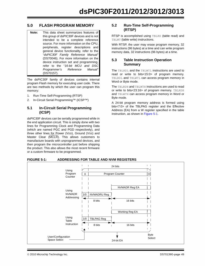
dsPIC30F2011/2012/3012/3013
5.0 FLASH PROGRAM MEMORY
The dsPIC30F family of devices contains internalprogram Flash memory for executing user code. Thereare two methods by which the user can program thismemory:
1. Run-Time Self-Programming (RTSP)2. In-Circuit Serial Programming™ (ICSP™)
5.1 In-Circuit Serial Programming (ICSP)
dsPIC30F devices can be serially programmed while inthe end application circuit. This is simply done with twolines for Programming Clock and Programming Data(which are named PGC and PGD respectively), andthree other lines for Power (VDD), Ground (VSS) andMaster Clear (MCLR). This allows customers tomanufacture boards with unprogrammed devices, andthen program the microcontroller just before shippingthe product. This also allows the most recent firmwareor a custom firmware to be programmed.
5.2 Run-Time Self-Programming (RTSP)
RTSP is accomplished using TBLRD (table read) andTBLWT (table write) instructions.
With RTSP, the user may erase program memory, 32instructions (96 bytes) at a time and can write programmemory data, 32 instructions (96 bytes) at a time.
5.3 Table Instruction Operation Summary
The TBLRDL and the TBLWTL instructions are used toread or write to bits<15:0> of program memory.TBLRDL and TBLWTL can access program memory inWord or Byte mode.
The TBLRDH and TBLWTH instructions are used to reador write to bits<23:16> of program memory. TBLRDHand TBLWTH can access program memory in Word orByte mode.
A 24-bit program memory address is formed usingbits<7:0> of the TBLPAG register and the EffectiveAddress (EA) from a W register specified in the tableinstruction, as shown in Figure 5-1.
FIGURE 5-1: ADDRESSING FOR TABLE AND NVM REGISTERS
Note: This data sheet summarizes features ofthis group of dsPIC30F devices and is notintended to be a complete referencesource. For more information on the CPU,peripherals, register descriptions andgeneral device functionality, refer to the“dsPIC30F Family Reference Manual”(DS70046). For more information on thedevice instruction set and programming,refer to the “16-bit MCU and DSCProgrammer’s Reference Manual”(DS70157).
0Program Counter
24 bits
NVMADRU Reg
8 bits 16 bits
Program
Using
TBLPAG Reg
8 bits
Working Reg EA
16 bits
Using
Byte
24-bit EA
1/0
0
1/0
Select
TableInstruction
NVMADRAddressing
Counter
Using
NVMADR Reg EA
User/ConfigurationSpace Select
© 2010 Microchip Technology Inc. DS70139G-page 49
dsPIC30F2011/2012/3012/3013
5.4 RTSP OperationThe dsPIC30F Flash program memory is organizedinto rows and panels. Each row consists of 32instructions or 96 bytes. Each panel consists of 128rows or 4K x 24 instructions. RTSP allows the user toerase one row (32 instructions) at a time and toprogram four instructions at one time. RTSP may beused to program multiple program memory panels, butthe table pointer must be changed at each panelboundary.Each panel of program memory contains write latchesthat hold 32 instructions of programming data. Prior tothe actual programming operation, the write data mustbe loaded into the panel write latches. The data to beprogrammed into the panel is loaded in sequentialorder into the write latches; instruction 0, instruction 1,etc. The instruction words loaded must always be froma 32 address boundary.
The basic sequence for RTSP programming is to set upa Table Pointer, then do a series of TBLWT instructionsto load the write latches. Programming is performed bysetting the special bits in the NVMCON register. 32TBLWTL and four TBLWTH instructions are required toload the 32 instructions. If multiple panel programmingis required, the Table Pointer needs to be changed andthe next set of multiple write latches written.
All of the table write operations are single-word writes(2 instruction cycles), because only the table latchesare written. A programming cycle is required forprogramming each row.
The Flash Program Memory is readable, writable anderasable during normal operation over the entire VDDrange.
5.5 Control RegistersThe four SFRs used to read and write the programFlash memory are:
• NVMCON• NVMADR• NVMADRU• NVMKEY
5.5.1 NVMCON REGISTERThe NVMCON register controls which blocks are to beerased, which memory type is to be programmed, andstart of the programming cycle.
5.5.2 NVMADR REGISTERThe NVMADR register is used to hold the lower twobytes of the Effective Address. The NVMADR registercaptures the EA<15:0> of the last table instruction thathas been executed and selects the row to write.
5.5.3 NVMADRU REGISTERThe NVMADRU register is used to hold the upper byteof the Effective Address. The NVMADRU registercaptures the EA<23:16> of the last table instructionthat has been executed.
5.5.4 NVMKEY REGISTERNVMKEY is a write-only register that is used for writeprotection. To start a programming or an erasesequence, the user must consecutively write 0x55 and0xAA to the NVMKEY register. Refer to Section 5.6“Programming Operations” for further details.
Note: The user can also directly write to theNVMADR and NVMADRU registers tospecify a program memory address forerasing or programming.
DS70139G-page 50 © 2010 Microchip Technology Inc.
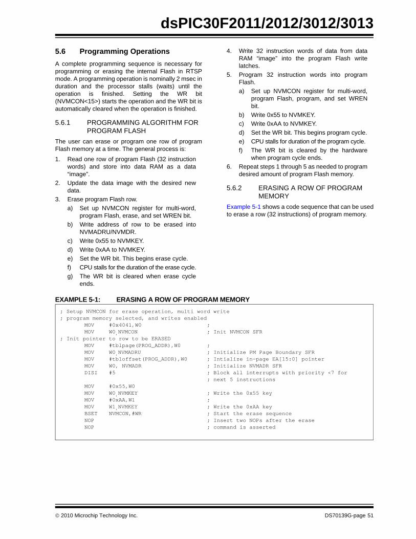
dsPIC30F2011/2012/3012/3013
5.6 Programming OperationsA complete programming sequence is necessary forprogramming or erasing the internal Flash in RTSPmode. A programming operation is nominally 2 msec induration and the processor stalls (waits) until theoperation is finished. Setting the WR bit(NVMCON<15>) starts the operation and the WR bit isautomatically cleared when the operation is finished.5.6.1 PROGRAMMING ALGORITHM FOR PROGRAM FLASH
The user can erase or program one row of programFlash memory at a time. The general process is:
1. Read one row of program Flash (32 instructionwords) and store into data RAM as a data“image”.
2. Update the data image with the desired newdata.
3. Erase program Flash row.a) Set up NVMCON register for multi-word,
program Flash, erase, and set WREN bit.b) Write address of row to be erased into
NVMADRU/NVMDR.c) Write 0x55 to NVMKEY.d) Write 0xAA to NVMKEY.e) Set the WR bit. This begins erase cycle.f) CPU stalls for the duration of the erase cycle.g) The WR bit is cleared when erase cycle
ends.
4. Write 32 instruction words of data from dataRAM “image” into the program Flash writelatches.
5. Program 32 instruction words into programFlash.a) Set up NVMCON register for multi-word,
program Flash, program, and set WRENbit.
b) Write 0x55 to NVMKEY.c) Write 0xAA to NVMKEY.d) Set the WR bit. This begins program cycle.e) CPU stalls for duration of the program cycle.f) The WR bit is cleared by the hardware
when program cycle ends.6. Repeat steps 1 through 5 as needed to program
desired amount of program Flash memory.
5.6.2 ERASING A ROW OF PROGRAM MEMORY
Example 5-1 shows a code sequence that can be usedto erase a row (32 instructions) of program memory.
EXAMPLE 5-1: ERASING A ROW OF PROGRAM MEMORY ; Setup NVMCON for erase operation, multi word write; program memory selected, and writes enabled
MOV #0x4041,W0 ;MOV W0,NVMCON ; Init NVMCON SFR
; Init pointer to row to be ERASEDMOV #tblpage(PROG_ADDR),W0 ; MOV W0,NVMADRU ; Initialize PM Page Boundary SFRMOV #tbloffset(PROG_ADDR),W0 ; Intialize in-page EA[15:0] pointerMOV W0, NVMADR ; Initialize NVMADR SFRDISI #5 ; Block all interrupts with priority <7 for
; next 5 instructionsMOV #0x55,W0MOV W0,NVMKEY ; Write the 0x55 key MOV #0xAA,W1 ;MOV W1,NVMKEY ; Write the 0xAA keyBSET NVMCON,#WR ; Start the erase sequence NOP ; Insert two NOPs after the eraseNOP ; command is asserted
© 2010 Microchip Technology Inc. DS70139G-page 51
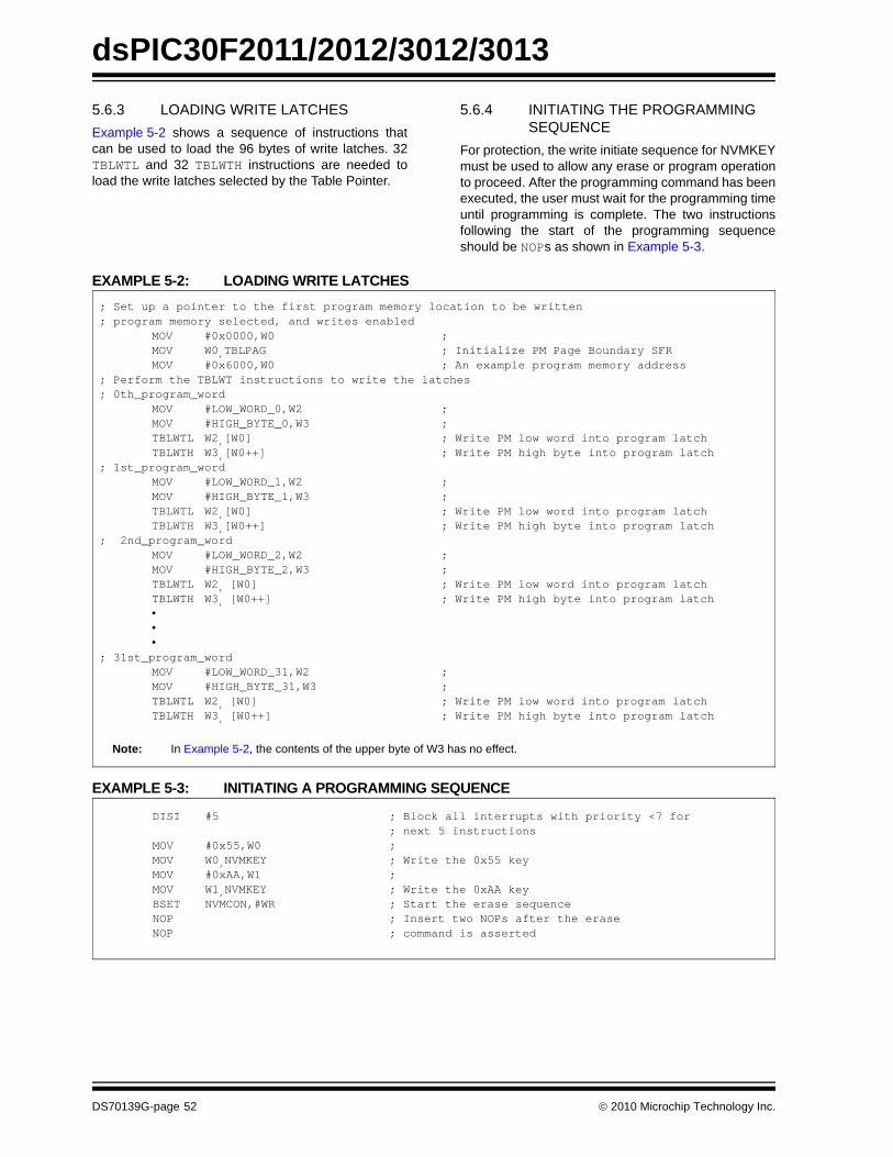
dsPIC30F2011/2012/3012/3013
5.6.3 LOADING WRITE LATCHESExample 5-2 shows a sequence of instructions thatcan be used to load the 96 bytes of write latches. 32TBLWTL and 32 TBLWTH instructions are needed toload the write latches selected by the Table Pointer.5.6.4 INITIATING THE PROGRAMMING SEQUENCE
For protection, the write initiate sequence for NVMKEYmust be used to allow any erase or program operationto proceed. After the programming command has beenexecuted, the user must wait for the programming timeuntil programming is complete. The two instructionsfollowing the start of the programming sequenceshould be NOPs as shown in Example 5-3.
EXAMPLE 5-2: LOADING WRITE LATCHES
EXAMPLE 5-3: INITIATING A PROGRAMMING SEQUENCE
; Set up a pointer to the first program memory location to be written; program memory selected, and writes enabled
MOV #0x0000,W0 ; MOV W0,TBLPAG ; Initialize PM Page Boundary SFRMOV #0x6000,W0 ; An example program memory address
; Perform the TBLWT instructions to write the latches; 0th_program_word
MOV #LOW_WORD_0,W2 ; MOV #HIGH_BYTE_0,W3 ; TBLWTL W2,[W0] ; Write PM low word into program latchTBLWTH W3,[W0++] ; Write PM high byte into program latch
; 1st_program_wordMOV #LOW_WORD_1,W2 ; MOV #HIGH_BYTE_1,W3 ; TBLWTL W2,[W0] ; Write PM low word into program latchTBLWTH W3,[W0++] ; Write PM high byte into program latch
; 2nd_program_wordMOV #LOW_WORD_2,W2 ; MOV #HIGH_BYTE_2,W3 ; TBLWTL W2, [W0] ; Write PM low word into program latchTBLWTH W3, [W0++] ; Write PM high byte into program latch•••
; 31st_program_wordMOV #LOW_WORD_31,W2 ; MOV #HIGH_BYTE_31,W3 ; TBLWTL W2, [W0] ; Write PM low word into program latchTBLWTH W3, [W0++] ; Write PM high byte into program latch
Note: In Example 5-2, the contents of the upper byte of W3 has no effect.
DISI #5 ; Block all interrupts with priority <7 for; next 5 instructions
MOV #0x55,W0 ; MOV W0,NVMKEY ; Write the 0x55 keyMOV #0xAA,W1 ;MOV W1,NVMKEY ; Write the 0xAA keyBSET NVMCON,#WR ; Start the erase sequence NOP ; Insert two NOPs after the eraseNOP ; command is asserted
DS70139G-page 52 © 2010 Microchip Technology Inc.
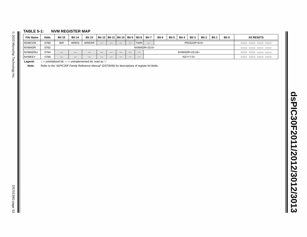
© 2010 M
icrochip Technology Inc.D
S70139G
-page 53
dsPIC30F2011/2012/3012/3013
TAF 1 Bit 0 All RESETS
NV 0000 0000 0000 0000
NV uuuu uuuu uuuu uuuu
NV 0000 0000 uuuu uuuu
NV 0000 0000 0000 0000
Le
BLE 5-1: NVM REGISTER MAPile Name Addr. Bit 15 Bit 14 Bit 13 Bit 12 Bit 11 Bit 10 Bit 9 Bit 8 Bit 7 Bit 6 Bit 5 Bit 4 Bit 3 Bit 2 Bit
MCON 0760 WR WREN WRERR — — — — TWRI — PROGOP<6:0>
MADR 0762 NVMADR<15:0>
MADRU 0764 — — — — — — — — NVMADR<23:16>
MKEY 0766 — — — — — — — — KEY<7:0>
gend: u = uninitialized bit; — = unimplemented bit, read as ‘0’Note: Refer to the “dsPIC30F Family Reference Manual” (DS70046) for descriptions of register bit fields.
dsPIC30F2011/2012/3012/3013
NOTES:DS70139G-page 54 © 2010 Microchip Technology Inc.
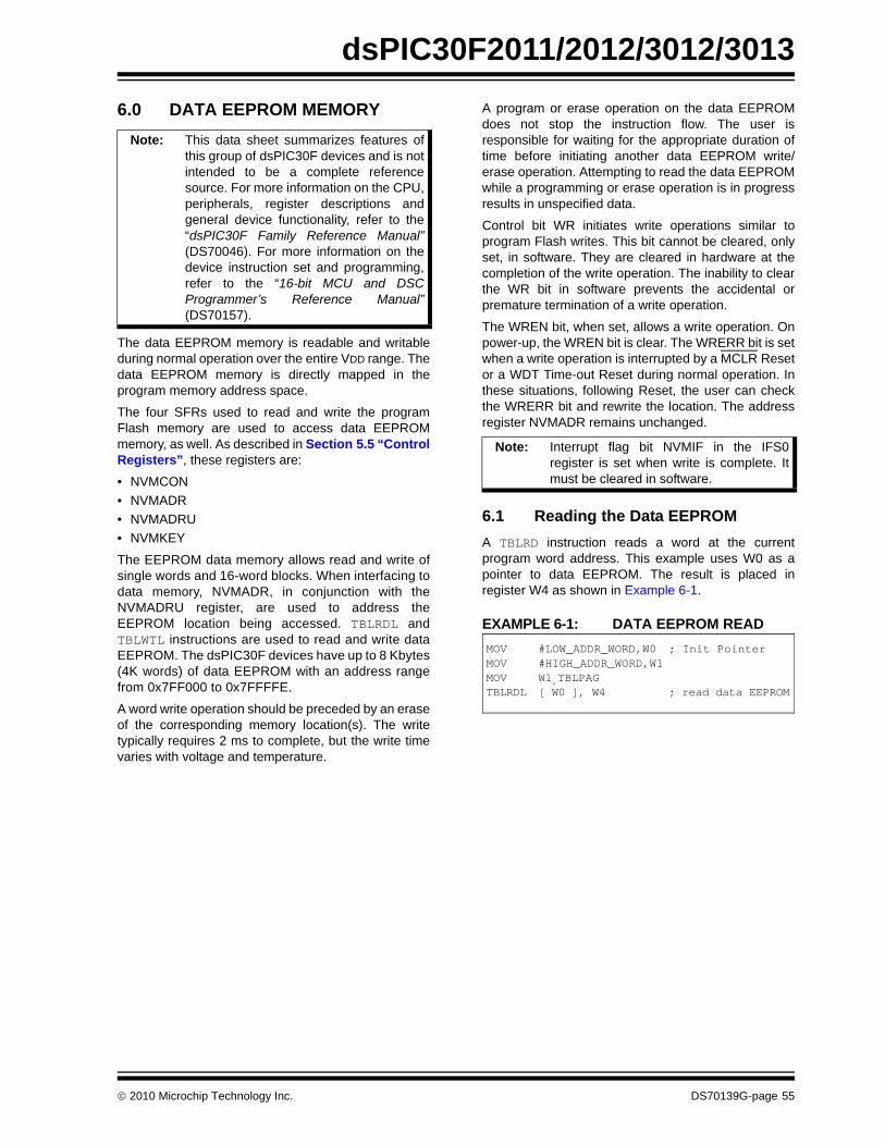
dsPIC30F2011/2012/3012/3013
6.0 DATA EEPROM MEMORY
The data EEPROM memory is readable and writableduring normal operation over the entire VDD range. Thedata EEPROM memory is directly mapped in theprogram memory address space.
The four SFRs used to read and write the programFlash memory are used to access data EEPROMmemory, as well. As described in Section 5.5 “ControlRegisters”, these registers are:
• NVMCON• NVMADR• NVMADRU• NVMKEY
The EEPROM data memory allows read and write ofsingle words and 16-word blocks. When interfacing todata memory, NVMADR, in conjunction with theNVMADRU register, are used to address theEEPROM location being accessed. TBLRDL andTBLWTL instructions are used to read and write dataEEPROM. The dsPIC30F devices have up to 8 Kbytes(4K words) of data EEPROM with an address rangefrom 0x7FF000 to 0x7FFFFE.
A word write operation should be preceded by an eraseof the corresponding memory location(s). The writetypically requires 2 ms to complete, but the write timevaries with voltage and temperature.
A program or erase operation on the data EEPROMdoes not stop the instruction flow. The user isresponsible for waiting for the appropriate duration oftime before initiating another data EEPROM write/erase operation. Attempting to read the data EEPROMwhile a programming or erase operation is in progressresults in unspecified data.
Control bit WR initiates write operations similar toprogram Flash writes. This bit cannot be cleared, onlyset, in software. They are cleared in hardware at thecompletion of the write operation. The inability to clearthe WR bit in software prevents the accidental orpremature termination of a write operation.
The WREN bit, when set, allows a write operation. Onpower-up, the WREN bit is clear. The WRERR bit is setwhen a write operation is interrupted by a MCLR Resetor a WDT Time-out Reset during normal operation. Inthese situations, following Reset, the user can checkthe WRERR bit and rewrite the location. The addressregister NVMADR remains unchanged.
6.1 Reading the Data EEPROM A TBLRD instruction reads a word at the currentprogram word address. This example uses W0 as apointer to data EEPROM. The result is placed inregister W4 as shown in Example 6-1.
EXAMPLE 6-1: DATA EEPROM READ
Note: This data sheet summarizes features ofthis group of dsPIC30F devices and is notintended to be a complete referencesource. For more information on the CPU,peripherals, register descriptions andgeneral device functionality, refer to the“dsPIC30F Family Reference Manual”(DS70046). For more information on thedevice instruction set and programming,refer to the “16-bit MCU and DSCProgrammer’s Reference Manual”(DS70157).
Note: Interrupt flag bit NVMIF in the IFS0register is set when write is complete. Itmust be cleared in software.
MOV #LOW_ADDR_WORD,W0 ; Init PointerMOV #HIGH_ADDR_WORD,W1MOV W1,TBLPAG TBLRDL [ W0 ], W4 ; read data EEPROM
© 2010 Microchip Technology Inc. DS70139G-page 55
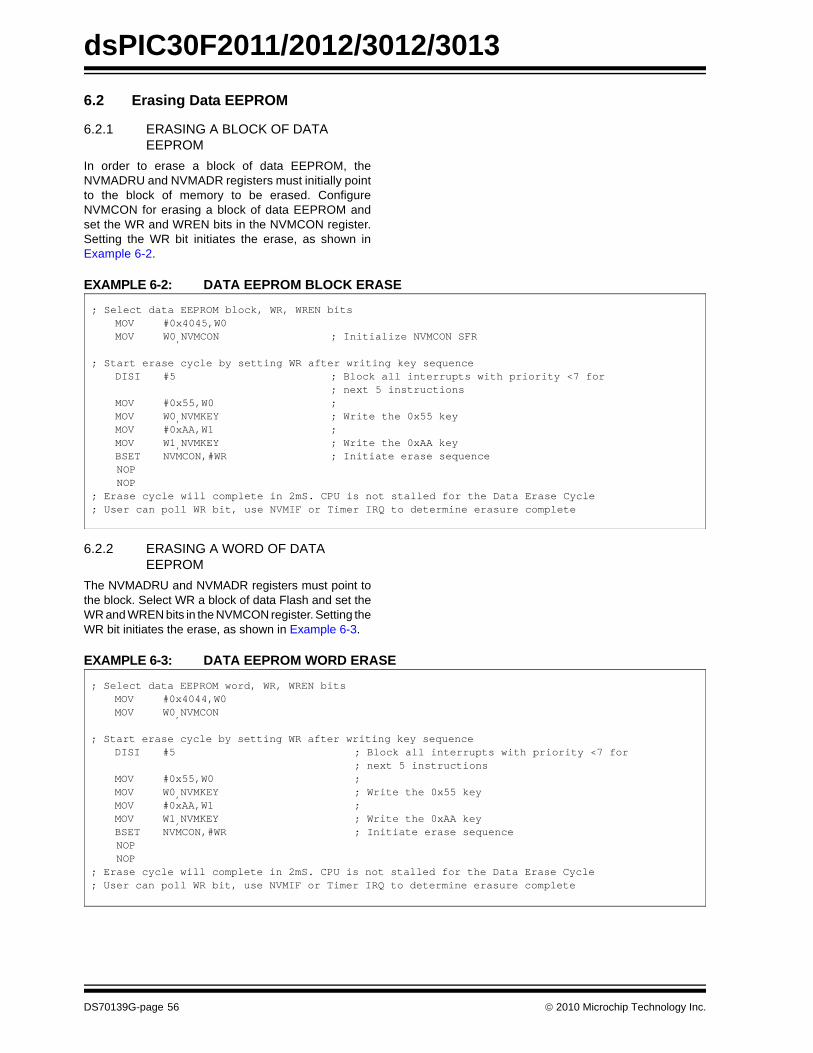
dsPIC30F2011/2012/3012/3013
6.2 Erasing Data EEPROM6.2.1 ERASING A BLOCK OF DATA EEPROM
In order to erase a block of data EEPROM, theNVMADRU and NVMADR registers must initially pointto the block of memory to be erased. ConfigureNVMCON for erasing a block of data EEPROM andset the WR and WREN bits in the NVMCON register.Setting the WR bit initiates the erase, as shown inExample 6-2.
EXAMPLE 6-2: DATA EEPROM BLOCK ERASE
6.2.2 ERASING A WORD OF DATA EEPROM
The NVMADRU and NVMADR registers must point tothe block. Select WR a block of data Flash and set theWR and WREN bits in the NVMCON register. Setting theWR bit initiates the erase, as shown in Example 6-3.
EXAMPLE 6-3: DATA EEPROM WORD ERASE
; Select data EEPROM block, WR, WREN bitsMOV #0x4045,W0MOV W0,NVMCON ; Initialize NVMCON SFR
; Start erase cycle by setting WR after writing key sequence
DISI #5 ; Block all interrupts with priority <7 for; next 5 instructions
MOV #0x55,W0 ; MOV W0,NVMKEY ; Write the 0x55 keyMOV #0xAA,W1 ;MOV W1,NVMKEY ; Write the 0xAA keyBSET NVMCON,#WR ; Initiate erase sequence
NOP NOP ; Erase cycle will complete in 2mS. CPU is not stalled for the Data Erase Cycle; User can poll WR bit, use NVMIF or Timer IRQ to determine erasure complete
; Select data EEPROM word, WR, WREN bitsMOV #0x4044,W0MOV W0,NVMCON
; Start erase cycle by setting WR after writing key sequence
DISI #5 ; Block all interrupts with priority <7 for; next 5 instructions
MOV #0x55,W0 ; MOV W0,NVMKEY ; Write the 0x55 key
MOV #0xAA,W1 ;MOV W1,NVMKEY ; Write the 0xAA key
BSET NVMCON,#WR ; Initiate erase sequence NOP NOP ; Erase cycle will complete in 2mS. CPU is not stalled for the Data Erase Cycle; User can poll WR bit, use NVMIF or Timer IRQ to determine erasure complete
DS70139G-page 56 © 2010 Microchip Technology Inc.
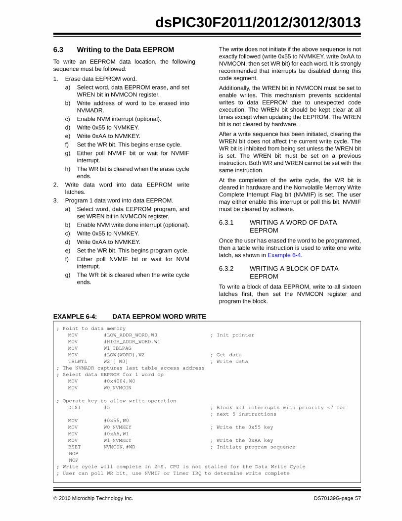
dsPIC30F2011/2012/3012/3013
6.3 Writing to the Data EEPROM To write an EEPROM data location, the followingsequence must be followed:1. Erase data EEPROM word.a) Select word, data EEPROM erase, and set
WREN bit in NVMCON register.b) Write address of word to be erased into
NVMADR.c) Enable NVM interrupt (optional).d) Write 0x55 to NVMKEY.e) Write 0xAA to NVMKEY.f) Set the WR bit. This begins erase cycle.g) Either poll NVMIF bit or wait for NVMIF
interrupt.h) The WR bit is cleared when the erase cycle
ends.2. Write data word into data EEPROM write
latches.3. Program 1 data word into data EEPROM.
a) Select word, data EEPROM program, andset WREN bit in NVMCON register.
b) Enable NVM write done interrupt (optional).c) Write 0x55 to NVMKEY.d) Write 0xAA to NVMKEY.e) Set the WR bit. This begins program cycle.f) Either poll NVMIF bit or wait for NVM
interrupt.g) The WR bit is cleared when the write cycle
ends.
The write does not initiate if the above sequence is notexactly followed (write 0x55 to NVMKEY, write 0xAA toNVMCON, then set WR bit) for each word. It is stronglyrecommended that interrupts be disabled during thiscode segment.
Additionally, the WREN bit in NVMCON must be set toenable writes. This mechanism prevents accidentalwrites to data EEPROM due to unexpected codeexecution. The WREN bit should be kept clear at alltimes except when updating the EEPROM. The WRENbit is not cleared by hardware.
After a write sequence has been initiated, clearing theWREN bit does not affect the current write cycle. TheWR bit is inhibited from being set unless the WREN bitis set. The WREN bit must be set on a previousinstruction. Both WR and WREN cannot be set with thesame instruction.
At the completion of the write cycle, the WR bit iscleared in hardware and the Nonvolatile Memory WriteComplete Interrupt Flag bit (NVMIF) is set. The usermay either enable this interrupt or poll this bit. NVMIFmust be cleared by software.
6.3.1 WRITING A WORD OF DATA EEPROM
Once the user has erased the word to be programmed,then a table write instruction is used to write one writelatch, as shown in Example 6-4.
6.3.2 WRITING A BLOCK OF DATA EEPROM
To write a block of data EEPROM, write to all sixteenlatches first, then set the NVMCON register andprogram the block.
EXAMPLE 6-4: DATA EEPROM WORD WRITE; Point to data memory
MOV #LOW_ADDR_WORD,W0 ; Init pointerMOV #HIGH_ADDR_WORD,W1MOV W1,TBLPAGMOV #LOW(WORD),W2 ; Get dataTBLWTL W2,[ W0] ; Write data
; The NVMADR captures last table access address; Select data EEPROM for 1 word op
MOV #0x4004,W0MOV W0,NVMCON
; Operate key to allow write operation
DISI #5 ; Block all interrupts with priority <7 for; next 5 instructions
MOV #0x55,W0MOV W0,NVMKEY ; Write the 0x55 keyMOV #0xAA,W1MOV W1,NVMKEY ; Write the 0xAA keyBSET NVMCON,#WR ; Initiate program sequence
NOP NOP ; Write cycle will complete in 2mS. CPU is not stalled for the Data Write Cycle; User can poll WR bit, use NVMIF or Timer IRQ to determine write complete
© 2010 Microchip Technology Inc. DS70139G-page 57
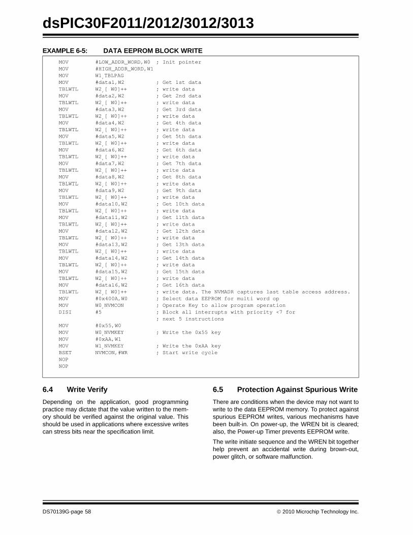
dsPIC30F2011/2012/3012/3013
EXAMPLE 6-5: DATA EEPROM BLOCK WRITE6.4 Write VerifyDepending on the application, good programmingpractice may dictate that the value written to the mem-ory should be verified against the original value. Thisshould be used in applications where excessive writescan stress bits near the specification limit.
6.5 Protection Against Spurious WriteThere are conditions when the device may not want towrite to the data EEPROM memory. To protect againstspurious EEPROM writes, various mechanisms havebeen built-in. On power-up, the WREN bit is cleared;also, the Power-up Timer prevents EEPROM write.
The write initiate sequence and the WREN bit togetherhelp prevent an accidental write during brown-out,power glitch, or software malfunction.
MOV #LOW_ADDR_WORD,W0 ; Init pointer MOV #HIGH_ADDR_WORD,W1 MOV W1,TBLPAG MOV #data1,W2 ; Get 1st data TBLWTL W2,[ W0]++ ; write data MOV #data2,W2 ; Get 2nd data TBLWTL W2,[ W0]++ ; write data MOV #data3,W2 ; Get 3rd data TBLWTL W2,[ W0]++ ; write data MOV #data4,W2 ; Get 4th data TBLWTL W2,[ W0]++ ; write data MOV #data5,W2 ; Get 5th data TBLWTL W2,[ W0]++ ; write data MOV #data6,W2 ; Get 6th data TBLWTL W2,[ W0]++ ; write data MOV #data7,W2 ; Get 7th data TBLWTL W2,[ W0]++ ; write data MOV #data8,W2 ; Get 8th data TBLWTL W2,[ W0]++ ; write data MOV #data9,W2 ; Get 9th data TBLWTL W2,[ W0]++ ; write data MOV #data10,W2 ; Get 10th data TBLWTL W2,[ W0]++ ; write data MOV #data11,W2 ; Get 11th data TBLWTL W2,[ W0]++ ; write data MOV #data12,W2 ; Get 12th data TBLWTL W2,[ W0]++ ; write data MOV #data13,W2 ; Get 13th data TBLWTL W2,[ W0]++ ; write data MOV #data14,W2 ; Get 14th data TBLWTL W2,[ W0]++ ; write data MOV #data15,W2 ; Get 15th data TBLWTL W2,[ W0]++ ; write data MOV #data16,W2 ; Get 16th data TBLWTL W2,[ W0]++ ; write data. The NVMADR captures last table access address. MOV #0x400A,W0 ; Select data EEPROM for multi word op MOV W0,NVMCON ; Operate Key to allow program operation
DISI #5 ; Block all interrupts with priority <7 for; next 5 instructions
MOV #0x55,W0 MOV W0,NVMKEY ; Write the 0x55 key MOV #0xAA,W1 MOV W1,NVMKEY ; Write the 0xAA key BSET NVMCON,#WR ; Start write cycle NOP NOP
DS70139G-page 58 © 2010 Microchip Technology Inc.
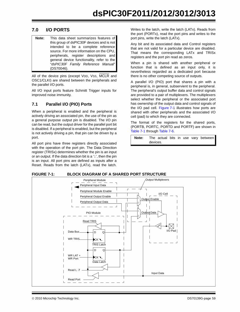
dsPIC30F2011/2012/3012/3013
7.0 I/O PORTS
All of the device pins (except VDD, VSS, MCLR andOSC1/CLKI) are shared between the peripherals andthe parallel I/O ports.
All I/O input ports feature Schmitt Trigger inputs forimproved noise immunity.
7.1 Parallel I/O (PIO) PortsWhen a peripheral is enabled and the peripheral isactively driving an associated pin, the use of the pin asa general purpose output pin is disabled. The I/O pincan be read, but the output driver for the parallel port bitis disabled. If a peripheral is enabled, but the peripheralis not actively driving a pin, that pin can be driven by aport.
All port pins have three registers directly associatedwith the operation of the port pin. The Data Directionregister (TRISx) determines whether the pin is an inputor an output. If the data direction bit is a ‘1’, then the pinis an input. All port pins are defined as inputs after aReset. Reads from the latch (LATx), read the latch.
Writes to the latch, write the latch (LATx). Reads fromthe port (PORTx), read the port pins and writes to theport pins, write the latch (LATx).
Any bit and its associated data and Control registersthat are not valid for a particular device are disabled.That means the corresponding LATx and TRISxregisters and the port pin read as zeros.
When a pin is shared with another peripheral orfunction that is defined as an input only, it isnevertheless regarded as a dedicated port becausethere is no other competing source of outputs.
A parallel I/O (PIO) port that shares a pin with aperipheral is, in general, subservient to the peripheral.The peripheral’s output buffer data and control signalsare provided to a pair of multiplexers. The multiplexersselect whether the peripheral or the associated porthas ownership of the output data and control signals ofthe I/O pad cell. Figure 7-1 illustrates how ports areshared with other peripherals and the associated I/Ocell (pad) to which they are connected.
The format of the registers for the shared ports,(PORTB, PORTC, PORTD and PORTF) are shown inTable 7-1 through Table 7-6.
FIGURE 7-1: BLOCK DIAGRAM OF A SHARED PORT STRUCTURE
Note: This data sheet summarizes features ofthis group of dsPIC30F devices and is notintended to be a complete referencesource. For more information on the CPU,peripherals, register descriptions andgeneral device functionality, refer to the“dsPIC30F Family Reference Manual”(DS70046).
Note: The actual bits in use vary betweendevices.
QD
CK
WR LAT +
TRIS Latch
I/O Pad
WR Port
Data Bus
QD
CKData Latch
Read LAT
Read Port
Read TRIS
1
0
1
0
WR TRIS
Peripheral Output DataOutput Enable
Peripheral Input Data
I/O Cell
Peripheral Module
Peripheral Output Enable
PIO Module
Output Multiplexers
Output Data
Input Data
Peripheral Module Enable
© 2010 Microchip Technology Inc. DS70139G-page 59
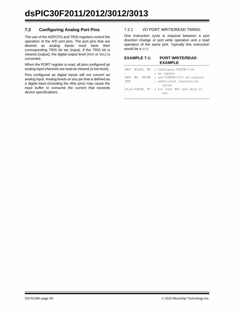
dsPIC30F2011/2012/3012/3013
7.2 Configuring Analog Port PinsThe use of the ADPCFG and TRIS registers control theoperation of the A/D port pins. The port pins that aredesired as analog inputs must have theircorresponding TRIS bit set (input). If the TRIS bit iscleared (output), the digital output level (VOH or VOL) isconverted.When the PORT register is read, all pins configured asanalog input channels are read as cleared (a low level).
Pins configured as digital inputs will not convert ananalog input. Analog levels on any pin that is defined asa digital input (including the ANx pins) may cause theinput buffer to consume the current that exceedsdevice specifications.
7.2.1 I/O PORT WRITE/READ TIMINGOne instruction cycle is required between a portdirection change or port write operation and a readoperation of the same port. Typically this instructionwould be a NOP.
EXAMPLE 7-1: PORT WRITE/READ EXAMPLE
MOV #0xF0, W0 ; Configure PORTB<7:4> ; as inputs
MOV W0, TRISB ; and PORTB<3:0> as outputsNOP ; additional instruction
cyclebtss PORTB, #7 ; bit test RB7 and skip if
set
DS70139G-page 60 © 2010 Microchip Technology Inc.
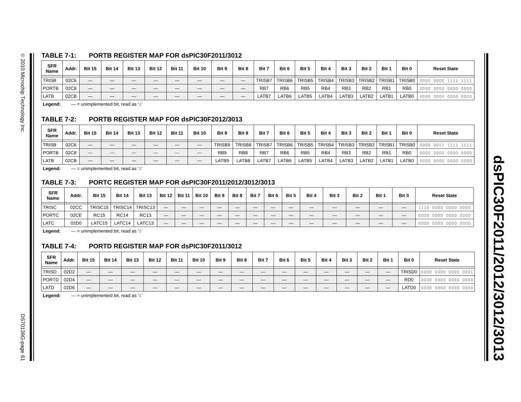
© 2010 M
icrochip Technology Inc.D
S70139G
-page 61
dsPIC30F2011/2012/3012/3013
TA
TA
TA
TA
N 2 Bit 1 Bit 0 Reset State
TR B2 TRISB1 TRISB0 0000 0000 1111 1111
PO 2 RB1 RB0 0000 0000 0000 0000
LA B2 LATB1 LATB0 0000 0000 0000 0000
Le
N 2 Bit 1 Bit 0 Reset State
TR B2 TRISB1 TRISB0 0000 0011 1111 1111
PO 2 RB1 RB0 0000 0000 0000 0000
LA B2 LATB1 LATB0 0000 0000 0000 0000
Le
N Bit 1 Bit 0 Reset State
TR — — 1110 0000 0000 0000
PO — — 0000 0000 0000 0000
LA — — 0000 0000 0000 0000
Le
SN 2 Bit 1 Bit 0 Reset State
TR — TRISD0 0000 0000 0000 0001
PO — RD0 0000 0000 0000 0000
LA — LATD0 0000 0000 0000 0000
Le
BLE 7-1: PORTB REGISTER MAP FOR dsPIC30F2011/3012
BLE 7-2: PORTB REGISTER MAP FOR dsPIC30F2012/3013
BLE 7-3: PORTC REGISTER MAP FOR dsPIC30F2011/2012/3012/3013
BLE 7-4: PORTD REGISTER MAP FOR dsPIC30F2011/3012
SFR ame Addr. Bit 15 Bit 14 Bit 13 Bit 12 Bit 11 Bit 10 Bit 9 Bit 8 Bit 7 Bit 6 Bit 5 Bit 4 Bit 3 Bit
ISB 02C6 — — — — — — — — TRISB7 TRISB6 TRISB5 TRISB4 TRISB3 TRIS
RTB 02C8 — — — — — — — — RB7 RB6 RB5 RB4 RB3 RB
TB 02CB — — — — — — — — LATB7 LATB6 LATB5 LATB4 LATB3 LAT
gend: — = unimplemented bit, read as ‘0’
SFR ame Addr. Bit 15 Bit 14 Bit 13 Bit 12 Bit 11 Bit 10 Bit 9 Bit 8 Bit 7 Bit 6 Bit 5 Bit 4 Bit 3 Bit
ISB 02C6 — — — — — — TRISB9 TRISB8 TRISB7 TRISB6 TRISB5 TRISB4 TRISB3 TRIS
RTB 02C8 — — — — — — RB9 RB8 RB7 RB6 RB5 RB4 RB3 RB
TB 02CB — — — — — — LATB9 LATB8 LATB7 LATB6 LATB5 LATB4 LATB3 LAT
gend: — = unimplemented bit, read as ‘0’
SFR ame Addr. Bit 15 Bit 14 Bit 13 Bit 12 Bit 11 Bit 10 Bit 9 Bit 8 Bit 7 Bit 6 Bit 5 Bit 4 Bit 3 Bit 2
ISC 02CC TRISC15 TRISC14 TRISC13 — — — — — — — — — — —
RTC 02CE RC15 RC14 RC13 — — — — — — — — — — —
TC 02D0 LATC15 LATC14 LATC13 — — — — — — — — — — —
gend: — = unimplemented bit, read as ‘0’
FR ame Addr. Bit 15 Bit 14 Bit 13 Bit 12 Bit 11 Bit 10 Bit 9 Bit 8 Bit 7 Bit 6 Bit 5 Bit 4 Bit 3 Bit
ISD 02D2 — — — — — — — — — — — — — —
RTD 02D4 — — — — — — — — — — — — — —
TD 02D6 — — — — — — — — — — — — — —
gend: — = unimplemented bit, read as ‘0’
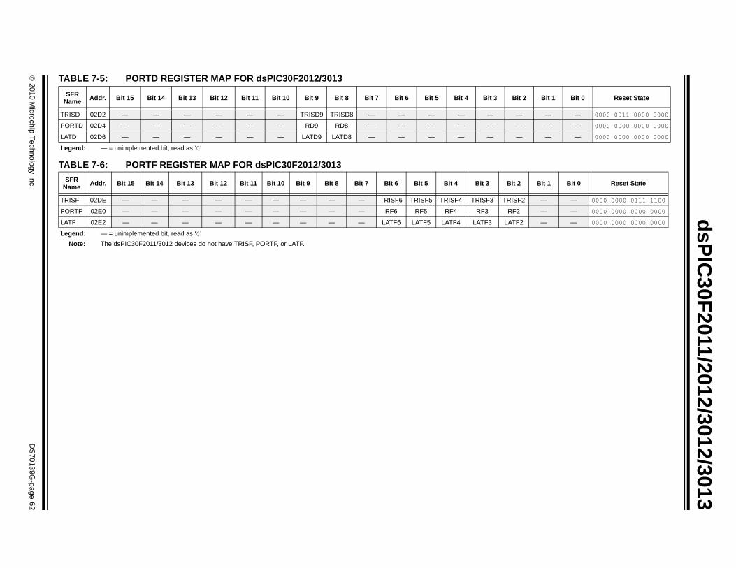
© 2010 M
icrochip Technology Inc.D
S70139G
-page 62
dsPIC30F2011/2012/3012/3013
TA
TA
SN 2 Bit 1 Bit 0 Reset State
TR — — 0000 0011 0000 0000
PO — — 0000 0000 0000 0000
LA — — 0000 0000 0000 0000
Le
SN Bit 1 Bit 0 Reset State
TR 2 — — 0000 0000 0111 1100
PO — — 0000 0000 0000 0000
LA 2 — — 0000 0000 0000 0000
Le
BLE 7-5: PORTD REGISTER MAP FOR dsPIC30F2012/3013
BLE 7-6: PORTF REGISTER MAP FOR dsPIC30F2012/3013
FR ame Addr. Bit 15 Bit 14 Bit 13 Bit 12 Bit 11 Bit 10 Bit 9 Bit 8 Bit 7 Bit 6 Bit 5 Bit 4 Bit 3 Bit
ISD 02D2 — — — — — — TRISD9 TRISD8 — — — — — —
RTD 02D4 — — — — — — RD9 RD8 — — — — — —
TD 02D6 — — — — — — LATD9 LATD8 — — — — — —
gend: — = unimplemented bit, read as ‘0’
FR ame Addr. Bit 15 Bit 14 Bit 13 Bit 12 Bit 11 Bit 10 Bit 9 Bit 8 Bit 7 Bit 6 Bit 5 Bit 4 Bit 3 Bit 2
ISF 02DE — — — — — — — — — TRISF6 TRISF5 TRISF4 TRISF3 TRISF
RTF 02E0 — — — — — — — — — RF6 RF5 RF4 RF3 RF2
TF 02E2 — — — — — — — — — LATF6 LATF5 LATF4 LATF3 LATF
gend: — = unimplemented bit, read as ‘0’Note: The dsPIC30F2011/3012 devices do not have TRISF, PORTF, or LATF.
dsPIC30F2011/2012/3012/3013
7.3 Input Change Notification ModuleThe input change notification module provides thedsPIC30F devices the ability to generate interruptrequests to the processor, in response to a change ofstate on selected input pins. This module is capable ofdetecting input change of states even in Sleep mode,when the clocks are disabled. There are up to 10external signals (CN0 through CN7, CN17 and CN18)that may be selected (enabled) for generating aninterrupt request on a change of state.TABLE 7-7: INPUT CHANGE NOTIFICATION REGISTER MAP FOR dsPIC30F2011/3012 (BITS 7-0)
TABLE 7-8: INPUT CHANGE NOTIFICATION REGISTER MAP FOR dsPIC30F2012/3013 (BITS 7-0)
SFR Name Address Bit 7 Bit 6 Bit 5 Bit 4 Bit 3 Bit 2 Bit 1 Bit 0 Reset State
CNEN1 00C0 CN7IE CN6IE CN5IE CN4IE CN3IE CN2IE CN1IE CN0IE 0000 0000 0000 0000
CNEN2 00C2 — — — — — — — — 0000 0000 0000 0000
CNPU1 00C4 CN7PUE CN6PUE CN5PUE CN4PUE CN3PUE CN2PUE CN1PUE CN0PUE 0000 0000 0000 0000
CNPU2 00C6 — — — — — — — — 0000 0000 0000 0000
Legend: — = unimplemented bit, read as ‘0’
SFR Name Address Bit 7 Bit 6 Bit 5 Bit 4 Bit 3 Bit 2 Bit 1 Bit 0 Reset State
CNEN1 00C0 CN7IE CN6IE CN5IE CN4IE CN3IE CN2IE CN1IE CN0IE 0000 0000 0000 0000
CNEN2 00C2 — — — — — CN18IE CN17IE — 0000 0000 0000 0000
CNPU1 00C4 CN7PUE CN6PUE CN5PUE CN4PUE CN3PUE CN2PUE CN1PUE CN0PUE 0000 0000 0000 0000
CNPU2 00C6 — — — — — CN18PUE CN17PUE — 0000 0000 0000 0000
Legend: — = unimplemented bit, read as ‘0’Note: Refer to the “dsPIC30F Family Reference Manual” (DS70046) for descriptions of register bit fields.
© 2010 Microchip Technology Inc. DS70139G-page 63

dsPIC30F2011/2012/3012/3013
NOTES:DS70139G-page 64 © 2010 Microchip Technology Inc.
dsPIC30F2011/2012/3012/3013
8.0 INTERRUPTS
The dsPIC30F sensor family has up to 21 interruptsources and 4 processor exceptions (traps) which mustbe arbitrated based on a priority scheme.
The CPU is responsible for reading the Interrupt VectorTable (IVT) and transferring the address contained inthe interrupt vector to the program counter. Theinterrupt vector is transferred from the program databus into the program counter via a 24-bit widemultiplexer on the input of the program counter.
The Interrupt Vector Table (IVT) and Alternate InterruptVector Table (AIVT) are placed near the beginning ofprogram memory (0x000004). The IVT and AIVT areshown in Figure 8-1.
The interrupt controller is responsible forpre-processing the interrupts and processorexceptions before they are presented to the processorcore. The peripheral interrupts and traps are enabled,prioritized and controlled using centralized SpecialFunction Registers (SFRs):
• IFS0<15:0>, IFS1<15:0>, IFS2<15:0>All interrupt request flags are maintained in these three registers. The flags are set by their respective peripherals or external signals and they are cleared via software.
• IEC0<15:0>, IEC1<15:0>, IEC2<15:0>All interrupt enable control bits are maintained in these three registers. These control bits are used to individually enable interrupts from the peripherals or external signals.
• IPC0<15:0> through IPC10<7:0>The user assignable priority level associated with each of these 41 interrupts is held centrally in these eleven registers.
• IPL<3:0> The current CPU priority level is explicitly stored in the IPL bits. IPL<3> is present in the CORCON register, whereas IPL<2:0> are present in the STATUS register (SR) in the processor core.
• INTCON1<15:0>, INTCON2<15:0>Global interrupt control functions are derived from these two registers. INTCON1 contains the control and status flags for the processor exceptions. The INTCON2 register controls the external interrupt request signal behavior and the use of the alternate vector table.
All interrupt sources can be user assigned to one of 7priority levels, 1 through 7, through the IPCx registers.Each interrupt source is associated with an interruptvector, as shown in Table 8-1. Levels 7 and 1 representthe highest and lowest maskable priorities, respec-tively.
If the NSTDIS bit (INTCON1<15>) is set, nesting ofinterrupts is prevented. Thus, if an interrupt is currentlybeing serviced, processing of a new interrupt isprevented even if the new interrupt is of higher prioritythan the one currently being serviced.
Certain interrupts have specialized control bits forfeatures like edge or level triggered interrupts,interrupt-on-change, etc. Control of these featuresremains within the peripheral module which generatesthe interrupt.
The DISI instruction can be used to disable theprocessing of interrupts of priorities 6 and lower for acertain number of instructions, during which the DISI bit(INTCON2<14>) remains set.
When an interrupt is serviced, the PC is loaded with theaddress stored in the vector location in programmemory that corresponds to the interrupt. There are 63different vectors within the IVT (refer to Table 8-1).These vectors are contained in locations 0x000004through 0x0000FE of program memory (refer toTable 8-1). These locations contain 24-bit addresses,and in order to preserve robustness, an address errortrap takes place if the PC attempts to fetch any of thesewords during normal execution. This preventsexecution of random data as a result of accidentallydecrementing a PC into vector space, accidentallymapping a data space address into vector space, or thePC rolling over to 0x000000 after reaching the end ofimplemented program memory space. Execution of aGOTO instruction to this vector space also generates anaddress error trap.
Note: This data sheet summarizes features ofthis group of dsPIC30F devices and is notintended to be a complete referencesource. For more information on the CPU,peripherals, register descriptions andgeneral device functionality, refer to the“dsPIC30F Family Reference Manual”(DS70046). For more information on thedevice instruction set and programming,refer to the “16-bit MCU and DSCProgrammer’s Reference Manual”(DS70157).
Note: Interrupt flag bits get set when an interruptcondition occurs, regardless of the state ofits corresponding enable bit. Usersoftware should ensure the appropriateinterrupt flag bits are clear prior toenabling an interrupt.
Note: Assigning a priority level of ‘0’ to aninterrupt source is equivalent to disablingthat interrupt.
Note: The IPL bits become read-only wheneverthe NSTDIS bit has been set to ‘1’.
© 2010 Microchip Technology Inc. DS70139G-page 65
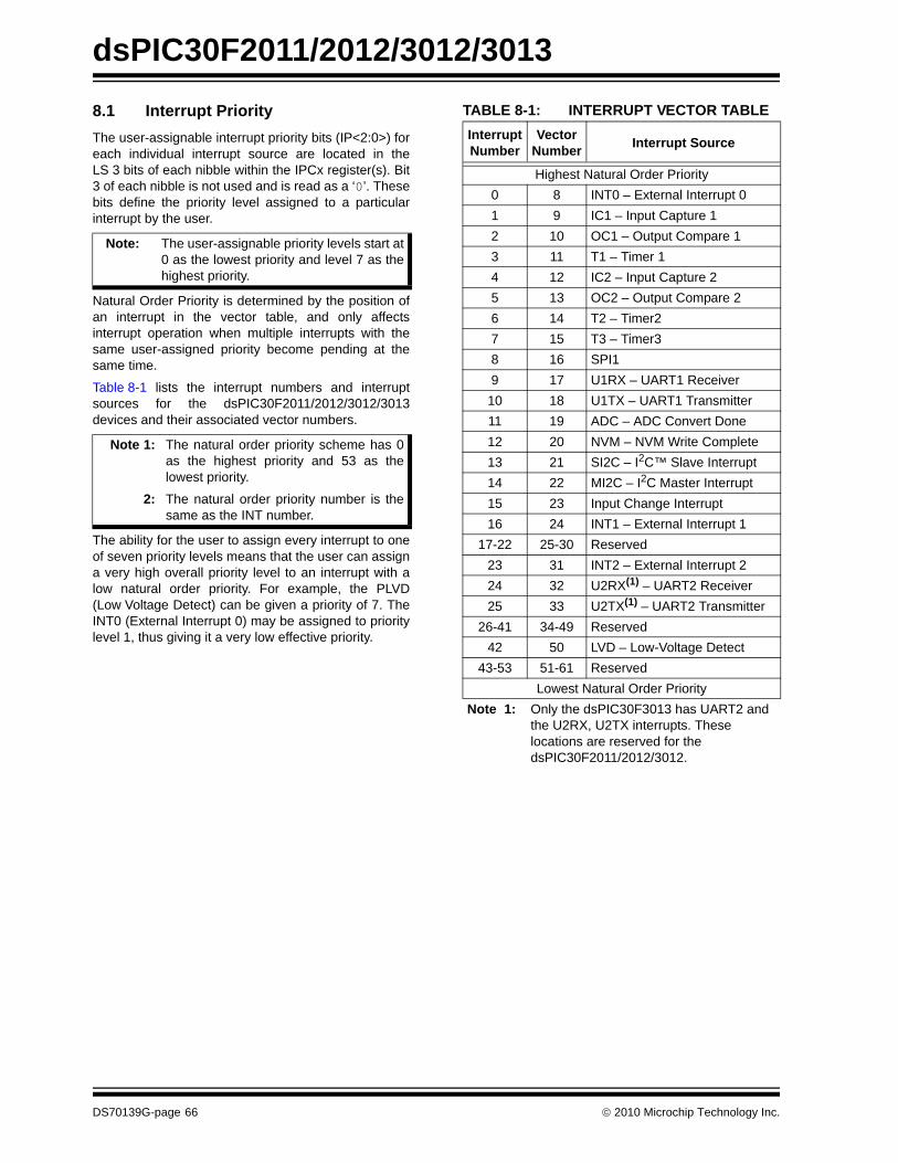
dsPIC30F2011/2012/3012/3013
8.1 Interrupt PriorityThe user-assignable interrupt priority bits (IP<2:0>) foreach individual interrupt source are located in theLS 3 bits of each nibble within the IPCx register(s). Bit3 of each nibble is not used and is read as a ‘0’. Thesebits define the priority level assigned to a particularinterrupt by the user.Natural Order Priority is determined by the position ofan interrupt in the vector table, and only affectsinterrupt operation when multiple interrupts with thesame user-assigned priority become pending at thesame time.
Table 8-1 lists the interrupt numbers and interruptsources for the dsPIC30F2011/2012/3012/3013devices and their associated vector numbers.
The ability for the user to assign every interrupt to oneof seven priority levels means that the user can assigna very high overall priority level to an interrupt with alow natural order priority. For example, the PLVD(Low Voltage Detect) can be given a priority of 7. TheINT0 (External Interrupt 0) may be assigned to prioritylevel 1, thus giving it a very low effective priority.
TABLE 8-1: INTERRUPT VECTOR TABLE
Note: The user-assignable priority levels start at0 as the lowest priority and level 7 as thehighest priority.
Note 1: The natural order priority scheme has 0as the highest priority and 53 as thelowest priority.
2: The natural order priority number is thesame as the INT number.
Interrupt Number
Vector Number Interrupt Source
Highest Natural Order Priority0 8 INT0 – External Interrupt 01 9 IC1 – Input Capture 12 10 OC1 – Output Compare 13 11 T1 – Timer 14 12 IC2 – Input Capture 25 13 OC2 – Output Compare 26 14 T2 – Timer27 15 T3 – Timer38 16 SPI1 9 17 U1RX – UART1 Receiver10 18 U1TX – UART1 Transmitter11 19 ADC – ADC Convert Done12 20 NVM – NVM Write Complete13 21 SI2C – I2C™ Slave Interrupt14 22 MI2C – I2C Master Interrupt15 23 Input Change Interrupt16 24 INT1 – External Interrupt 1
17-22 25-30 Reserved23 31 INT2 – External Interrupt 224 32 U2RX(1) – UART2 Receiver25 33 U2TX(1) – UART2 Transmitter
26-41 34-49 Reserved 42 50 LVD – Low-Voltage Detect
43-53 51-61 ReservedLowest Natural Order Priority
Note 1: Only the dsPIC30F3013 has UART2 and the U2RX, U2TX interrupts. These locations are reserved for the dsPIC30F2011/2012/3012.
DS70139G-page 66 © 2010 Microchip Technology Inc.
dsPIC30F2011/2012/3012/3013
8.2 Reset SequenceA Reset is not a true exception because the interruptcontroller is not involved in the Reset process. Theprocessor initializes its registers in response to a Resetwhich forces the PC to zero. The processor then beginsprogram execution at location 0x000000. A GOTOinstruction is stored in the first program memorylocation immediately followed by the address target forthe GOTO instruction. The processor executes the GOTOto the specified address and then begins operation atthe specified target (start) address.8.2.1 RESET SOURCESIn addition to external Reset and Power-on Reset(POR), there are six sources of error conditions which‘trap’ to the Reset vector.
• Watchdog Time-out:The watchdog has timed out, indicating that the processor is no longer executing the correct flow of code.
• Uninitialized W Register Trap:An attempt to use an uninitialized W register as an Address Pointer causes a Reset.
• Illegal Instruction Trap:Attempted execution of any unused opcodes results in an illegal instruction trap. Note that a fetch of an illegal instruction does not result in an illegal instruction trap if that instruction is flushed prior to execution due to a flow change.
• Brown-out Reset (BOR):A momentary dip in the power supply to the device has been detected which may result in malfunction.
• Trap Lockout:Occurrence of multiple trap conditions simultaneously causes a Reset.
8.3 TrapsTraps can be considered as non-maskable interruptsindicating a software or hardware error, which adhereto a predefined priority as shown in Figure 8-1. Theyare intended to provide the user a means to correcterroneous operation during debug and when operatingwithin the application.
Note that many of these trap conditions can only bedetected when they occur. Consequently, thequestionable instruction is allowed to complete prior totrap exception processing. If the user chooses torecover from the error, the result of the erroneousaction that caused the trap may have to be corrected.
There are eight fixed priority levels for traps: Level 8through Level 15, which implies that the IPL3 is alwaysset during processing of a trap.
If the user is not currently executing a trap, and he setsthe IPL<3:0> bits to a value of ‘0111’ (Level 7), then allinterrupts are disabled, but traps can still be processed.
8.3.1 TRAP SOURCESThe following traps are provided with increasingpriority. However, since all traps can be nested, priorityhas little effect.
Math Error Trap:The math error trap executes under the following fourcircumstances:
1. If an attempt is made to divide by zero, thedivide operation is aborted on a cycle boundaryand the trap is taken.
2. If enabled, a math error trap is taken when anarithmetic operation on either accumulator A orB causes an overflow from bit 31 and theaccumulator guard bits are not utilized.
3. If enabled, a math error trap is taken when anarithmetic operation on either accumulator A orB causes a catastrophic overflow from bit 39 andall saturation is disabled.
4. If the shift amount specified in a shift instructionis greater than the maximum allowed shiftamount, a trap occurs.
Note: If the user does not intend to takecorrective action in the event of a traperror condition, these vectors must beloaded with the address of a defaulthandler that contains the RESET instruc-tion. If, on the other hand, one of the vec-tors containing an invalid address iscalled, an address error trap is generated.
© 2010 Microchip Technology Inc. DS70139G-page 67
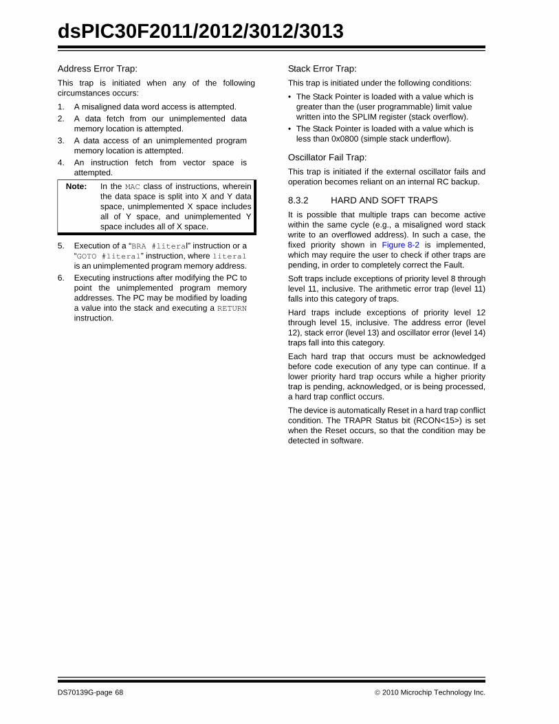
dsPIC30F2011/2012/3012/3013
Address Error Trap:This trap is initiated when any of the followingcircumstances occurs:1. A misaligned data word access is attempted.2. A data fetch from our unimplemented data
memory location is attempted.3. A data access of an unimplemented program
memory location is attempted.4. An instruction fetch from vector space is
attempted.
5. Execution of a “BRA #literal” instruction or a“GOTO #literal” instruction, where literalis an unimplemented program memory address.
6. Executing instructions after modifying the PC topoint the unimplemented program memoryaddresses. The PC may be modified by loadinga value into the stack and executing a RETURNinstruction.
Stack Error Trap:This trap is initiated under the following conditions:
• The Stack Pointer is loaded with a value which is greater than the (user programmable) limit value written into the SPLIM register (stack overflow).
• The Stack Pointer is loaded with a value which is less than 0x0800 (simple stack underflow).
Oscillator Fail Trap:This trap is initiated if the external oscillator fails andoperation becomes reliant on an internal RC backup.
8.3.2 HARD AND SOFT TRAPSIt is possible that multiple traps can become activewithin the same cycle (e.g., a misaligned word stackwrite to an overflowed address). In such a case, thefixed priority shown in Figure 8-2 is implemented,which may require the user to check if other traps arepending, in order to completely correct the Fault.
Soft traps include exceptions of priority level 8 throughlevel 11, inclusive. The arithmetic error trap (level 11)falls into this category of traps.
Hard traps include exceptions of priority level 12through level 15, inclusive. The address error (level12), stack error (level 13) and oscillator error (level 14)traps fall into this category.
Each hard trap that occurs must be acknowledgedbefore code execution of any type can continue. If alower priority hard trap occurs while a higher prioritytrap is pending, acknowledged, or is being processed,a hard trap conflict occurs.
The device is automatically Reset in a hard trap conflictcondition. The TRAPR Status bit (RCON<15>) is setwhen the Reset occurs, so that the condition may bedetected in software.
Note: In the MAC class of instructions, whereinthe data space is split into X and Y dataspace, unimplemented X space includesall of Y space, and unimplemented Yspace includes all of X space.
DS70139G-page 68 © 2010 Microchip Technology Inc.
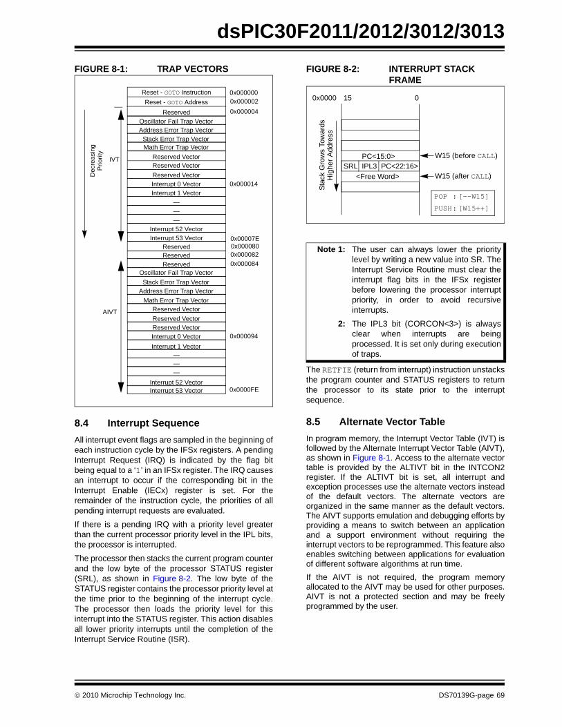
dsPIC30F2011/2012/3012/3013
FIGURE 8-1: TRAP VECTORS8.4 Interrupt SequenceAll interrupt event flags are sampled in the beginning ofeach instruction cycle by the IFSx registers. A pendingInterrupt Request (IRQ) is indicated by the flag bitbeing equal to a ‘1’ in an IFSx register. The IRQ causesan interrupt to occur if the corresponding bit in theInterrupt Enable (IECx) register is set. For theremainder of the instruction cycle, the priorities of allpending interrupt requests are evaluated.
If there is a pending IRQ with a priority level greaterthan the current processor priority level in the IPL bits,the processor is interrupted.
The processor then stacks the current program counterand the low byte of the processor STATUS register(SRL), as shown in Figure 8-2. The low byte of theSTATUS register contains the processor priority level atthe time prior to the beginning of the interrupt cycle.The processor then loads the priority level for thisinterrupt into the STATUS register. This action disablesall lower priority interrupts until the completion of theInterrupt Service Routine (ISR).
FIGURE 8-2: INTERRUPT STACK FRAME
The RETFIE (return from interrupt) instruction unstacksthe program counter and STATUS registers to returnthe processor to its state prior to the interruptsequence.
8.5 Alternate Vector TableIn program memory, the Interrupt Vector Table (IVT) isfollowed by the Alternate Interrupt Vector Table (AIVT),as shown in Figure 8-1. Access to the alternate vectortable is provided by the ALTIVT bit in the INTCON2register. If the ALTIVT bit is set, all interrupt andexception processes use the alternate vectors insteadof the default vectors. The alternate vectors areorganized in the same manner as the default vectors.The AIVT supports emulation and debugging efforts byproviding a means to switch between an applicationand a support environment without requiring theinterrupt vectors to be reprogrammed. This feature alsoenables switching between applications for evaluationof different software algorithms at run time.If the AIVT is not required, the program memoryallocated to the AIVT may be used for other purposes.AIVT is not a protected section and may be freelyprogrammed by the user.
Address Error Trap Vector
Oscillator Fail Trap VectorStack Error Trap Vector
Reserved VectorMath Error Trap Vector
Reserved
Oscillator Fail Trap VectorAddress Error Trap Vector
Reserved VectorReserved VectorInterrupt 0 VectorInterrupt 1 Vector
———
Interrupt 52 VectorInterrupt 53 Vector
Math Error Trap Vector
Dec
reas
ing
Prio
rity
0x000000
0x000014
Reserved
Stack Error Trap Vector
Reserved VectorReserved VectorInterrupt 0 VectorInterrupt 1 Vector
———
Interrupt 52 VectorInterrupt 53 Vector
IVT
AIVT
0x0000800x00007E
0x0000FE
Reserved
0x000094
Reset - GOTO InstructionReset - GOTO Address 0x000002
Reserved0x0000820x000084
0x000004
Reserved Vector
Note 1: The user can always lower the prioritylevel by writing a new value into SR. TheInterrupt Service Routine must clear theinterrupt flag bits in the IFSx registerbefore lowering the processor interruptpriority, in order to avoid recursiveinterrupts.
2: The IPL3 bit (CORCON<3>) is alwaysclear when interrupts are beingprocessed. It is set only during executionof traps.
<Free Word>
015
W15 (before CALL)
W15 (after CALL)
Stac
k G
row
s To
war
dsH
ighe
r Add
ress
0x0000
PC<15:0> SRL IPL3 PC<22:16>
POP : [--W15]
PUSH: [W15++]
© 2010 Microchip Technology Inc. DS70139G-page 69
dsPIC30F2011/2012/3012/3013
8.6 Fast Context SavingA context saving option is available using shadowregisters. Shadow registers are provided for the DC, N,OV, Z and C bits in SR, and the registers W0 throughW3. The shadows are only one level deep. The shadowregisters are accessible using the PUSH.S and POP.Sinstructions only. When the processor vectors to an interrupt, thePUSH.S instruction can be used to store the currentvalue of the aforementioned registers into theirrespective shadow registers. If an ISR of a certain priority uses the PUSH.S andPOP.S instructions for fast context saving, then ahigher priority ISR should not include the same instruc-tions. Users must save the key registers in softwareduring a lower priority interrupt if the higher priority ISRuses fast context saving.8.7 External Interrupt RequestsThe interrupt controller supports three externalinterrupt request signals, INT0-INT2. These inputs areedge sensitive; they require a low-to-high or ahigh-to-low transition to generate an interrupt request.The INTCON2 register has three bits, INT0EP-INT2EP,that select the polarity of the edge detection circuitry.
8.8 Wake-up from Sleep and IdleThe interrupt controller may be used to wake-up theprocessor from either Sleep or Idle modes, if Sleep orIdle mode is active when the interrupt is generated.If an enabled interrupt request of sufficient priority isreceived by the interrupt controller, then the standardinterrupt request is presented to the processor. At thesame time, the processor wakes up from Sleep or Idleand begins execution of the ISR needed to process theinterrupt request.
DS70139G-page 70 © 2010 Microchip Technology Inc.
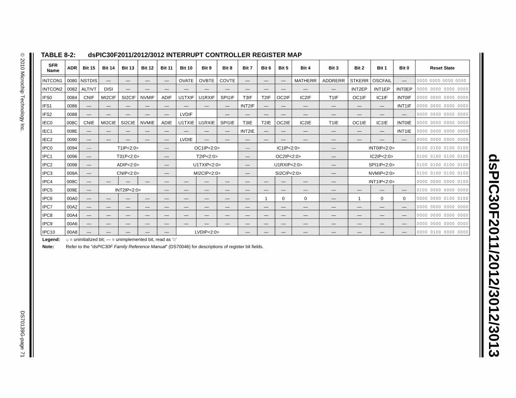
© 2010 M
icrochip Technology Inc.D
S70139G
-page 71
dsPIC30F2011/2012/3012/3013
TA
N Bit 1 Bit 0 Reset State
IN R OSCFAIL — 0000 0000 0000 0000
INT P INT1EP INT0EP 0000 0000 0000 0000
IFS IC1IF INT0IF 0000 0000 0000 0000
IFS — INT1IF 0000 0000 0000 0000
IFS — — 0000 0000 0000 0000
IEC IC1IE INT0IE 0000 0000 0000 0000
IEC — INT1IE 0000 0000 0000 0000
IEC — — 0000 0000 0000 0000
IPC INT0IP<2:0> 0100 0100 0100 0100
IPC IC2IP<2:0> 0100 0100 0100 0100
IPC SPI1IP<2:0> 0100 0100 0100 0100
IPC NVMIP<2:0> 0100 0100 0100 0100
IPC INT1IP<2:0> 0000 0000 0000 0100
IPC — — 0100 0000 0000 0000
IPC 0 0 0000 0000 0100 0100
IPC — — 0000 0000 0000 0000
IPC — — 0000 0000 0000 0000
IPC — — 0000 0000 0000 0000
IPC — — 0000 0100 0000 0000
LeNo
BLE 8-2: dsPIC30F2011/2012/3012 INTERRUPT CONTROLLER REGISTER MAPSFR ame ADR Bit 15 Bit 14 Bit 13 Bit 12 Bit 11 Bit 10 Bit 9 Bit 8 Bit 7 Bit 6 Bit 5 Bit 4 Bit 3 Bit 2
TCON1 0080 NSTDIS — — — — OVATE OVBTE COVTE — — — MATHERR ADDRERR STKER
CON2 0082 ALTIVT DISI — — — — — — — — — — — INT2E
0 0084 CNIF MI2CIF SI2CIF NVMIF ADIF U1TXIF U1RXIF SPI1IF T3IF T2IF OC2IF IC2IF T1IF OC1IF
1 0086 — — — — — — — — INT2IF — — — — —
2 0088 — — — — — LVDIF — — — — — — —
0 008C CNIE MI2CIE SI2CIE NVMIE ADIE U1TXIE U1RXIE SPI1IE T3IE T2IE OC2IE IC2IE T1IE OC1IE
1 008E — — — — — — — — INT2IE — — — — —
2 0090 — — — — — LVDIE — — — — — — — —
0 0094 — T1IP<2:0> — OC1IP<2:0> — IC1IP<2:0> —
1 0096 — T31P<2:0> — T2IP<2:0> — OC2IP<2:0> —
2 0098 — ADIP<2:0> — U1TXIP<2:0> — U1RXIP<2:0> —
3 009A — CNIP<2:0> — MI2CIP<2:0> — SI2CIP<2:0> —
4 009C — — — — — — — — — — — — —
5 009E — INT2IP<2:0> — — — — — — — — — —
6 00A0 — — — — — — — — — 1 0 0 — 1
7 00A2 — — — — — — — — — — — — — —
8 00A4 — — — — — — — — — — — — — —
9 00A6 — — — — — — — — — — — — — —
10 00A8 — — — — — LVDIP<2:0> — — — — — —gend: u = uninitialized bit; — = unimplemented bit, read as ‘0’te: Refer to the “dsPIC30F Family Reference Manual” (DS70046) for descriptions of register bit fields.
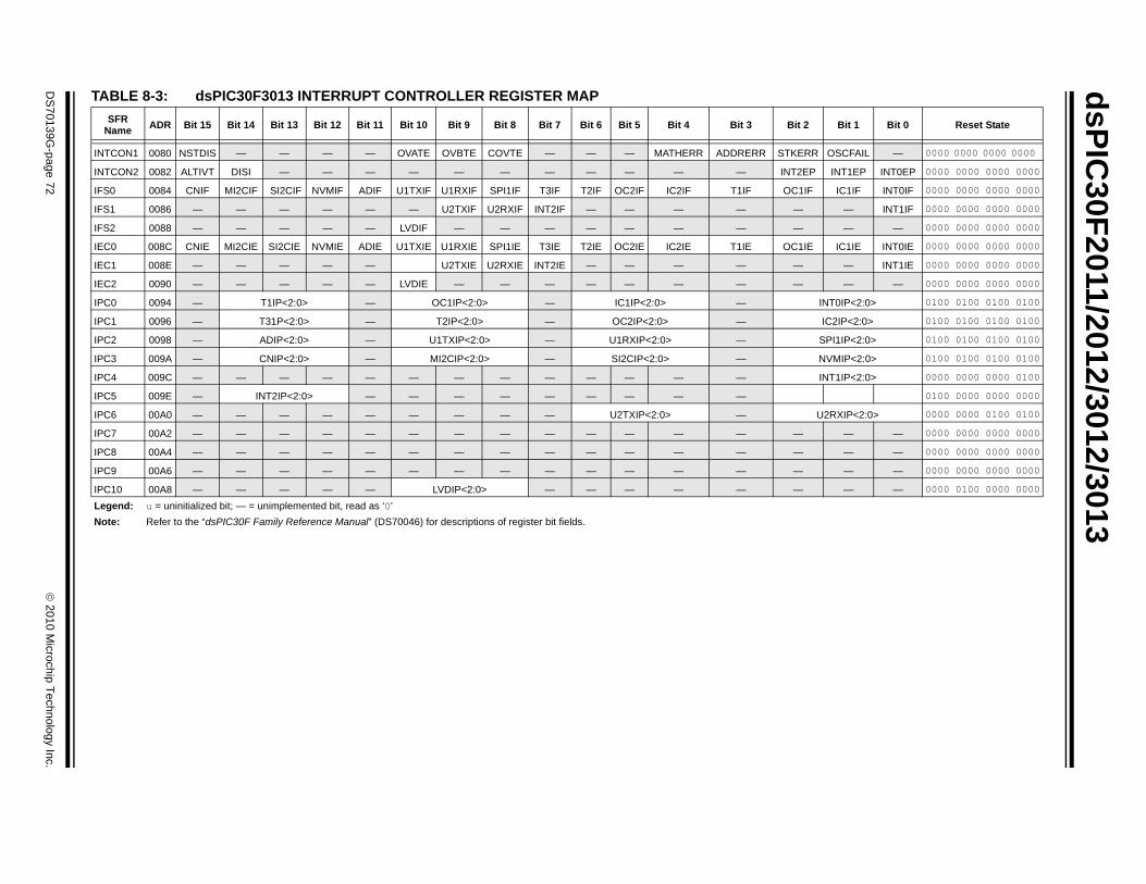
dsPIC30F2011/2012/3012/3013
DS
70139G-page 72
© 2010 M
icrochip Technology Inc.
Bit 2 Bit 1 Bit 0 Reset State
TKERR OSCFAIL — 0000 0000 0000 0000
NT2EP INT1EP INT0EP 0000 0000 0000 0000
OC1IF IC1IF INT0IF 0000 0000 0000 0000
— — INT1IF 0000 0000 0000 0000
— — — 0000 0000 0000 0000
OC1IE IC1IE INT0IE 0000 0000 0000 0000
— — INT1IE 0000 0000 0000 0000
— — — 0000 0000 0000 0000
INT0IP<2:0> 0100 0100 0100 0100
IC2IP<2:0> 0100 0100 0100 0100
SPI1IP<2:0> 0100 0100 0100 0100
NVMIP<2:0> 0100 0100 0100 0100
INT1IP<2:0> 0000 0000 0000 0100
0100 0000 0000 0000
U2RXIP<2:0> 0000 0000 0100 0100
— — — 0000 0000 0000 0000
— — — 0000 0000 0000 0000
— — — 0000 0000 0000 0000
— — — 0000 0100 0000 0000
TABLE 8-3: dsPIC30F3013 INTERRUPT CONTROLLER REGISTER MAPSFR
Name ADR Bit 15 Bit 14 Bit 13 Bit 12 Bit 11 Bit 10 Bit 9 Bit 8 Bit 7 Bit 6 Bit 5 Bit 4 Bit 3
INTCON1 0080 NSTDIS — — — — OVATE OVBTE COVTE — — — MATHERR ADDRERR S
INTCON2 0082 ALTIVT DISI — — — — — — — — — — — I
IFS0 0084 CNIF MI2CIF SI2CIF NVMIF ADIF U1TXIF U1RXIF SPI1IF T3IF T2IF OC2IF IC2IF T1IF
IFS1 0086 — — — — — — U2TXIF U2RXIF INT2IF — — — —
IFS2 0088 — — — — — LVDIF — — — — — — —
IEC0 008C CNIE MI2CIE SI2CIE NVMIE ADIE U1TXIE U1RXIE SPI1IE T3IE T2IE OC2IE IC2IE T1IE
IEC1 008E — — — — — U2TXIE U2RXIE INT2IE — — — —
IEC2 0090 — — — — — LVDIE — — — — — — —
IPC0 0094 — T1IP<2:0> — OC1IP<2:0> — IC1IP<2:0> —
IPC1 0096 — T31P<2:0> — T2IP<2:0> — OC2IP<2:0> —
IPC2 0098 — ADIP<2:0> — U1TXIP<2:0> — U1RXIP<2:0> —
IPC3 009A — CNIP<2:0> — MI2CIP<2:0> — SI2CIP<2:0> —
IPC4 009C — — — — — — — — — — — — —
IPC5 009E — INT2IP<2:0> — — — — — — — — —
IPC6 00A0 — — — — — — — — — U2TXIP<2:0> —
IPC7 00A2 — — — — — — — — — — — — —
IPC8 00A4 — — — — — — — — — — — — —
IPC9 00A6 — — — — — — — — — — — — —
IPC10 00A8 — — — — — LVDIP<2:0> — — — — —Legend: u = uninitialized bit; — = unimplemented bit, read as ‘0’Note: Refer to the “dsPIC30F Family Reference Manual” (DS70046) for descriptions of register bit fields.
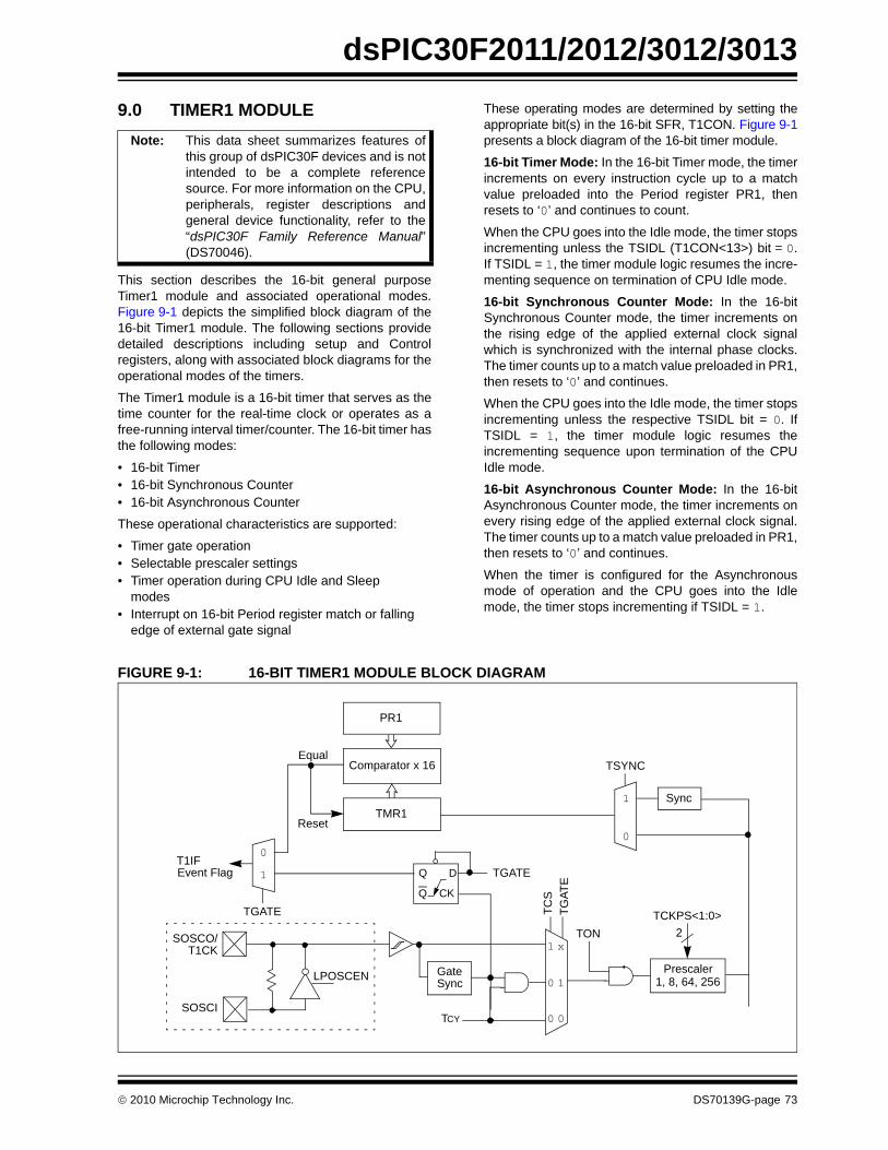
dsPIC30F2011/2012/3012/3013
9.0 TIMER1 MODULE
This section describes the 16-bit general purposeTimer1 module and associated operational modes.Figure 9-1 depicts the simplified block diagram of the16-bit Timer1 module. The following sections providedetailed descriptions including setup and Controlregisters, along with associated block diagrams for theoperational modes of the timers.
The Timer1 module is a 16-bit timer that serves as thetime counter for the real-time clock or operates as afree-running interval timer/counter. The 16-bit timer hasthe following modes:
• 16-bit Timer• 16-bit Synchronous Counter• 16-bit Asynchronous Counter
These operational characteristics are supported:
• Timer gate operation• Selectable prescaler settings• Timer operation during CPU Idle and Sleep
modes• Interrupt on 16-bit Period register match or falling
edge of external gate signal
These operating modes are determined by setting theappropriate bit(s) in the 16-bit SFR, T1CON. Figure 9-1presents a block diagram of the 16-bit timer module.
16-bit Timer Mode: In the 16-bit Timer mode, the timerincrements on every instruction cycle up to a matchvalue preloaded into the Period register PR1, thenresets to ‘0’ and continues to count.
When the CPU goes into the Idle mode, the timer stopsincrementing unless the TSIDL (T1CON<13>) bit = 0.If TSIDL = 1, the timer module logic resumes the incre-menting sequence on termination of CPU Idle mode.
16-bit Synchronous Counter Mode: In the 16-bitSynchronous Counter mode, the timer increments onthe rising edge of the applied external clock signalwhich is synchronized with the internal phase clocks.The timer counts up to a match value preloaded in PR1,then resets to ‘0’ and continues.
When the CPU goes into the Idle mode, the timer stopsincrementing unless the respective TSIDL bit = 0. IfTSIDL = 1, the timer module logic resumes theincrementing sequence upon termination of the CPUIdle mode.
16-bit Asynchronous Counter Mode: In the 16-bitAsynchronous Counter mode, the timer increments onevery rising edge of the applied external clock signal.The timer counts up to a match value preloaded in PR1,then resets to ‘0’ and continues.
When the timer is configured for the Asynchronousmode of operation and the CPU goes into the Idlemode, the timer stops incrementing if TSIDL = 1.
FIGURE 9-1: 16-BIT TIMER1 MODULE BLOCK DIAGRAM
Note: This data sheet summarizes features ofthis group of dsPIC30F devices and is notintended to be a complete referencesource. For more information on the CPU,peripherals, register descriptions andgeneral device functionality, refer to the“dsPIC30F Family Reference Manual”(DS70046).
TON
Sync
SOSCI
SOSCO/
PR1
T1IF
EqualComparator x 16
TMR1Reset
LPOSCEN
Event Flag
1
0
TSYNC
Q
Q D
CK
TGATE
TCKPS<1:0>
Prescaler1, 8, 64, 256
2
TGATE
TCY
1
0
T1CK
TCS
1 x
0 1
TGAT
E
0 0
GateSync
© 2010 Microchip Technology Inc. DS70139G-page 73
dsPIC30F2011/2012/3012/3013
9.1 Timer Gate OperationThe 16-bit timer can be placed in the Gated TimeAccumulation mode. This mode allows the internal TCYto increment the respective timer when the gate inputsignal (T1CK pin) is asserted high. Control bit,TGATE (T1CON<6>), must be set to enable this mode.The timer must be enabled (TON = 1) and the timerclock source set to internal (TCS = 0).When the CPU goes into Idle mode, the timer stopsincrementing unless TSIDL = 0. If TSIDL = 1, the timerresumes the incrementing sequence upon terminationof the CPU Idle mode.
9.2 Timer PrescalerThe input clock (FOSC/4 or external clock) to the 16-bitTimer has a prescale option of 1:1, 1:8, 1:64 and 1:256,selected by control bits, TCKPS<1:0> (T1CON<5:4>).The prescaler counter is cleared when any of thefollowing occurs:
• A write to the TMR1 register• A write to the T1CON register• A device Reset, such as a POR and BOR
However, if the timer is disabled (TON = 0), then thetimer prescaler cannot be reset since the prescalerclock is halted.
The TMR1 register is not cleared when the T1CONregister is written. It is cleared by writing to the TMR1register.
9.3 Timer Operation During Sleep ModeThe timer operates during CPU Sleep mode, if:
• The timer module is enabled (TON = 1), and • The timer clock source is selected as external
(TCS = 1), and• The TSYNC bit (T1CON<2>) is asserted to a logic
‘0’ which defines the external clock source as asynchronous.
When all three conditions are true, the timer continuesto count up to the Period register and be reset to0x0000.
When a match between the timer and the Periodregister occurs, an interrupt can be generated if therespective timer interrupt enable bit is asserted.
9.4 Timer InterruptThe 16-bit timer has the ability to generate aninterrupt-on-period match. When the timer countmatches the Period register, the T1IF bit is asserted andan interrupt is generated, if enabled. The T1IF bit must becleared in software. The timer interrupt flag, T1IF, islocated in the IFS0 Control register in the interruptcontroller.
When the Gated Time Accumulation mode is enabled,an interrupt is also generated on the falling edge of thegate signal (at the end of the accumulation cycle).
Enabling an interrupt is accomplished via therespective timer interrupt enable bit, T1IE. The timerinterrupt enable bit is located in the IEC0 Controlregister in the interrupt controller.
9.5 Real-Time ClockTimer1, when operating in Real-Time Clock (RTC)mode, provides time of day and event time-stampingcapabilities. Key operational features of the RTC are:
• Operation from 32 kHz LP oscillator• 8-bit prescaler• Low power • Real-Time Clock interrupts
These operating modes are determined by setting theappropriate bit(s) in the T1CON register.
FIGURE 9-2: RECOMMENDED COMPONENTS FOR TIMER1 LP OSCILLATOR RTC
9.5.1 RTC OSCILLATOR OPERATIONWhen the TON = 1, TCS = 1 and TGATE = 0, the timerincrements on the rising edge of the 32 kHz LP oscilla-tor output signal, up to the value specified in the Periodregister and is then reset to ‘0’.
The TSYNC bit must be asserted to a logic ‘0’(Asynchronous mode) for correct operation.
Enabling the LPOSCEN bit (OSCCON<1>) disablesthe normal Timer and Counter modes and enables atimer carry-out wake-up event.
When the CPU enters Sleep mode, the RTC continuesto operate, provided the 32 kHz external crystaloscillator is active and the control bits have not beenchanged. The TSIDL bit should be cleared to ‘0’ inorder for RTC to continue operation in Idle mode.
9.5.2 RTC INTERRUPTSWhen an interrupt event occurs, the respective interruptflag, T1IF, is asserted and an interrupt is generated ifenabled. The T1IF bit must be cleared in software. Therespective Timer interrupt flag, T1IF, is located in theIFS0 register in the interrupt controller.
SOSCI
SOSCO
R
C1
C2
dsPIC30FXXXX32.768 kHzXTAL
C1 = C2 = 18 pF; R = 100K
DS70139G-page 74 © 2010 Microchip Technology Inc.
dsPIC30F2011/2012/3012/3013
Enabling an interrupt is accomplished via therespective timer interrupt enable bit, T1IE. The timerinterrupt enable bit is located in the IEC0 Controlregister in the interrupt controller.© 2010 Microchip Technology Inc. DS70139G-page 75
dsPIC30F2011/2012/3012/3013
DS
70139G-page 76
© 2010 M
icrochip Technology Inc.
Bit 2 Bit 1 Bit 0 Reset State
uuuu uuuu uuuu uuuu
1111 1111 1111 1111
SYNC TCS — 0000 0000 0000 0000
TABLE 9-1: TIMER1 REGISTER MAPSFR Name Addr. Bit 15 Bit 14 Bit 13 Bit 12 Bit 11 Bit 10 Bit 9 Bit 8 Bit 7 Bit 6 Bit 5 Bit 4 Bit 3
TMR1 0100 Timer1 Register
PR1 0102 Period Register 1
T1CON 0104 TON — TSIDL — — — — — — TGATE TCKPS1 TCKPS0 — T
Legend: u = uninitialized bit; — = unimplemented bit, read as ‘0’Note: Refer to the “dsPIC30F Family Reference Manual” (DS70046) for descriptions of register bit fields.
dsPIC30F2011/2012/3012/3013
10.0 TIMER2/3 MODULE
This section describes the 32-bit general purposeTimer module (Timer2/3) and associated Operationalmodes. Figure 10-1 depicts the simplified blockdiagram of the 32-bit Timer2/3 module. Figure 10-2and Figure 10-3 show Timer2/3 configured as twoindependent 16-bit timers, Timer2 and Timer3,respectively.
The Timer2/3 module is a 32-bit timer (which can beconfigured as two 16-bit timers) with selectableoperating modes. These timers are utilized by otherperipheral modules, such as:
• Input Capture• Output Compare/Simple PWM
The following sections provide a detailed description,including setup and Control registers, along withassociated block diagrams for the operational modes ofthe timers.
The 32-bit timer has the following modes:
• Two independent 16-bit timers (Timer2 and Timer3) with all 16-bit operating modes (except Asynchronous Counter mode)
• Single 32-bit timer operation• Single 32-bit synchronous counter
Further, the following operational characteristics aresupported:
• ADC event trigger• Timer gate operation• Selectable prescaler settings• Timer operation during Idle and Sleep modes• Interrupt on a 32-bit period register match
These operating modes are determined by setting theappropriate bit(s) in the 16-bit T2CON and T3CONSFRs.
For 32-bit timer/counter operation, Timer2 is the ls wordand Timer3 is the ms word of the 32-bit timer.
16-bit Timer Mode: In the 16-bit mode, Timer2 andTimer3 can be configured as two independent 16-bittimers. Each timer can be set up in either 16-bit Timermode or 16-bit Synchronous Counter mode. SeeSection 9.0 “Timer1 Module” for details on these twooperating modes.
The only functional difference between Timer2 andTimer3 is that Timer2 provides synchronization of theclock prescaler output. This is useful for high frequencyexternal clock inputs.
32-bit Timer Mode: In the 32-bit Timer mode, the timerincrements on every instruction cycle, up to a matchvalue preloaded into the combined 32-bit Periodregister PR3/PR2, then resets to ‘0’ and continues tocount.
For synchronous 32-bit reads of the Timer2/Timer3pair, reading the ls word (TMR2 register) causes the msword to be read and latched into a 16-bit holdingregister, termed TMR3HLD.
For synchronous 32-bit writes, the holding register(TMR3HLD) must first be written to. When followed bya write to the TMR2 register, the contents of TMR3HLDis transferred and latched into the MSB of the 32-bittimer (TMR3).
32-bit Synchronous Counter Mode: In the 32-bitSynchronous Counter mode, the timer increments onthe rising edge of the applied external clock signalwhich is synchronized with the internal phase clocks.The timer counts up to a match value preloaded in thecombined 32-bit period register, PR3/PR2, then resetsto ‘0’ and continues.
When the timer is configured for the SynchronousCounter mode of operation and the CPU goes into theIdle mode, the timer stops incrementing unless theTSIDL bit (T2CON<13>) = 0. If TSIDL = 1, the timermodule logic resumes the incrementing sequenceupon termination of the CPU Idle mode.
Note: This data sheet summarizes features ofthis group of dsPIC30F devices and is notintended to be a complete referencesource. For more information on the CPU,peripherals, register descriptions andgeneral device functionality, refer to the“dsPIC30F Family Reference Manual“(DS70046).
Note: For 32-bit timer operation, T3CON controlbits are ignored. Only T2CON control bitsare used for setup and control. Timer2clock and gate inputs are utilized for the32-bit timer module, but an interrupt isgenerated with the Timer3 interrupt flag(T3IF) and the interrupt is enabled with theTimer3 interrupt enable bit (T3IE).
© 2010 Microchip Technology Inc. DS70139G-page 77
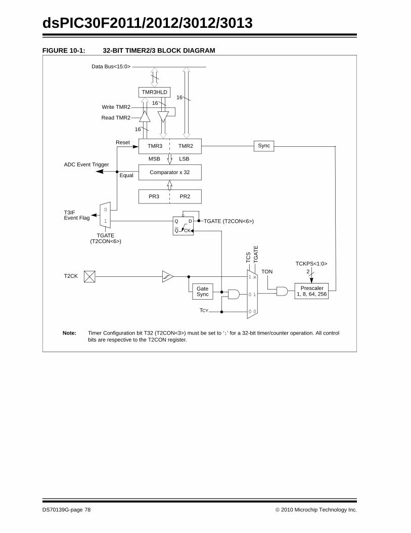
dsPIC30F2011/2012/3012/3013
FIGURE 10-1: 32-BIT TIMER2/3 BLOCK DIAGRAMTMR3 TMR2
T3IF
Equal Comparator x 32
PR3 PR2
Reset
LSB MSB
Event Flag
Note: Timer Configuration bit T32 (T2CON<3>) must be set to ‘1’ for a 32-bit timer/counter operation. All controlbits are respective to the T2CON register.
Data Bus<15:0>
Read TMR2
Write TMR216
16
16
Q
Q D
CK
TGATE (T2CON<6>)
(T2CON<6>)TGATE
0
1
TON
TCKPS<1:0>2
TCY
TC
S
1 x
0 1
TGAT
E
0 0
Gate
T2CK
Sync
ADC Event Trigger
Sync
TMR3HLD
Prescaler1, 8, 64, 256
DS70139G-page 78 © 2010 Microchip Technology Inc.
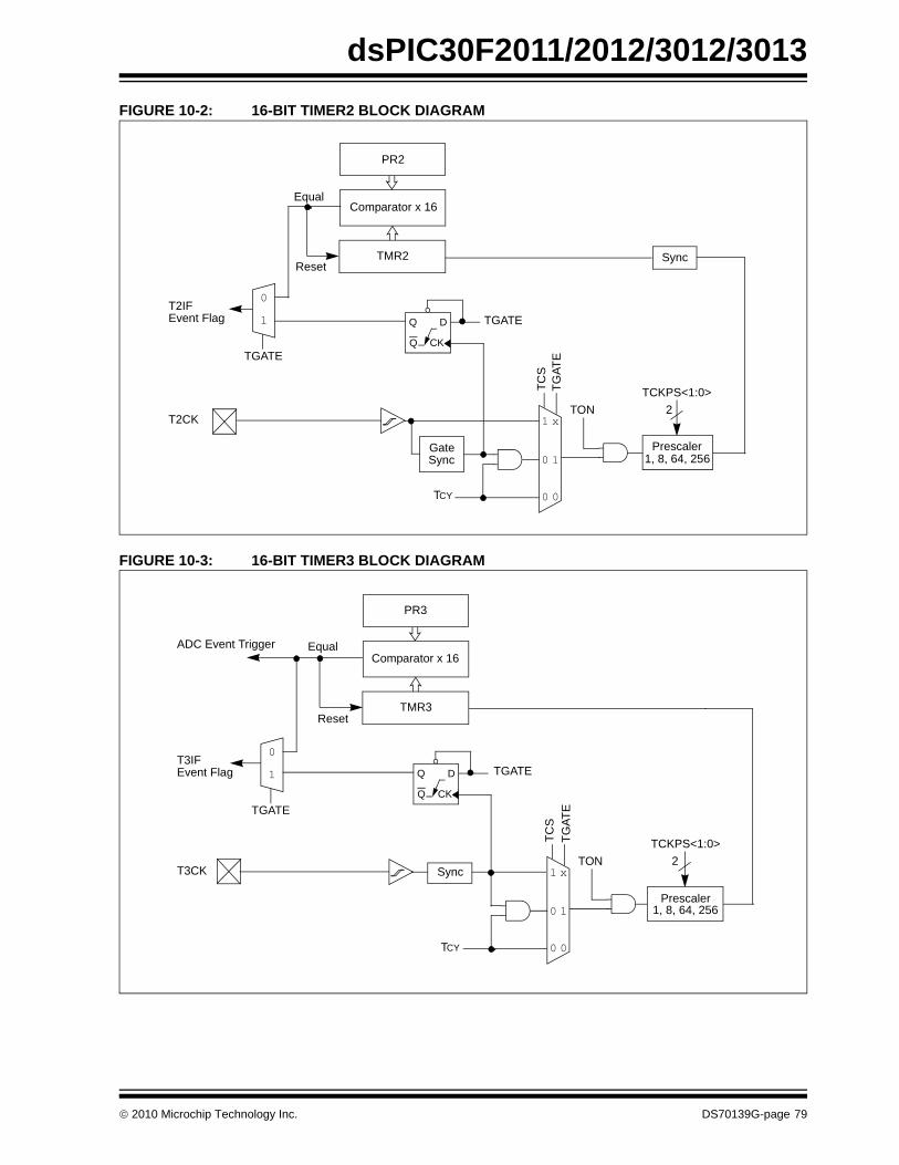
dsPIC30F2011/2012/3012/3013
FIGURE 10-2: 16-BIT TIMER2 BLOCK DIAGRAMFIGURE 10-3: 16-BIT TIMER3 BLOCK DIAGRAM
TON
Sync
PR2
T2IF
EqualComparator x 16
TMR2Reset
Event Flag TGATE
TCKPS<1:0>2
TGATE
TCY
1
0
TCS
1 x
0 1
TGAT
E
0 0
Gate
T2CK
SyncPrescaler
1, 8, 64, 256
Q
Q D
CK
TON
PR3
T3IF
EqualComparator x 16
TMR3Reset
Event Flag TGATE
TCKPS<1:0>2
TGATE
TCY
1
0
TCS
1 x
0 1
TGAT
E
0 0
T3CK
ADC Event Trigger
Sync
Q
Q D
CK
Prescaler1, 8, 64, 256
© 2010 Microchip Technology Inc. DS70139G-page 79
dsPIC30F2011/2012/3012/3013
10.1 Timer Gate OperationThe 32-bit timer can be placed in the Gated TimeAccumulation mode. This mode allows the internal TCYto increment the respective timer when the gate inputsignal (T2CK pin) is asserted high. Control bit, TGATE(T2CON<6>), must be set to enable this mode. Whenin this mode, Timer2 is the originating clock source.The TGATE setting is ignored for Timer3. The timermust be enabled (TON = 1) and the timer clock sourceset to internal (TCS = 0).The falling edge of the external signal terminates thecount operation but does not reset the timer. The usermust reset the timer in order to start counting from zero.
10.2 ADC Event TriggerWhen a match occurs between the 32-bit timer(TMR3/TMR2) and the 32-bit combined period register(PR3/PR2), or between the 16-bit timer TMR3 and the16-bit period register PR3, a special ADC trigger eventsignal is generated by Timer3.
10.3 Timer PrescalerThe input clock (FOSC/4 or external clock) to the timerhas a prescale option of 1:1, 1:8, 1:64, and 1:256,selected by control bits, TCKPS<1:0> (T2CON<5:4>and T3CON<5:4>). For the 32-bit timer operation, theoriginating clock source is Timer2. The prescaleroperation for Timer3 is not applicable in this mode. Theprescaler counter is cleared when any of the followingoccurs:
• A write to the TMR2/TMR3 register• A write to the T2CON/T3CON register• A device Reset, such as a POR and BOR
However, if the timer is disabled (TON = 0), the Timer2 prescaler cannot be reset since the prescaler clock ishalted.
TMR2/TMR3 is not cleared when T2CON/T3CON iswritten.
10.4 Timer Operation During Sleep Mode
The timer does not operate during CPU Sleep modebecause the internal clocks are disabled.
10.5 Timer InterruptThe 32-bit timer module can generate aninterrupt-on-period match or on the falling edge of theexternal gate signal. When the 32-bit timer countmatches the respective 32-bit period register, or thefalling edge of the external “gate” signal is detected, theT3IF bit (IFS0<7>) is asserted and an interrupt isgenerated if enabled. In this mode, the T3IF interruptflag is used as the source of the interrupt. The T3IF bitmust be cleared in software.
Enabling an interrupt is accomplished via therespective timer interrupt enable bit, T3IE (IEC0<7>).
DS70139G-page 80 © 2010 Microchip Technology Inc.
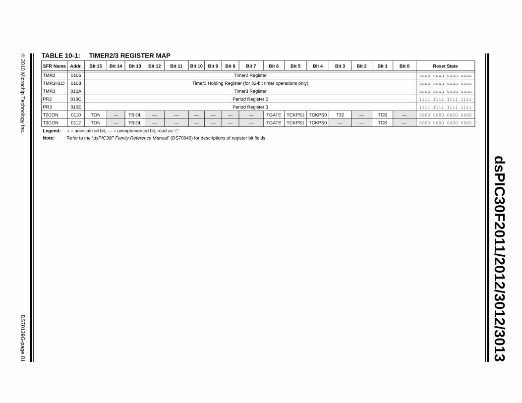
© 2010 M
icrochip Technology Inc.D
S70139G
-page 81
dsPIC30F2011/2012/3012/3013
TASF Bit 1 Bit 0 Reset State
TM uuuu uuuu uuuu uuuu
TM uuuu uuuu uuuu uuuu
TM uuuu uuuu uuuu uuuu
PR 1111 1111 1111 1111
PR 1111 1111 1111 1111
T2 TCS — 0000 0000 0000 0000
T3 TCS — 0000 0000 0000 0000
LeNo
BLE 10-1: TIMER2/3 REGISTER MAPR Name Addr. Bit 15 Bit 14 Bit 13 Bit 12 Bit 11 Bit 10 Bit 9 Bit 8 Bit 7 Bit 6 Bit 5 Bit 4 Bit 3 Bit 2
R2 0106 Timer2 Register
R3HLD 0108 Timer3 Holding Register (for 32-bit timer operations only)
R3 010A Timer3 Register
2 010C Period Register 2
3 010E Period Register 3
CON 0110 TON — TSIDL — — — — — — TGATE TCKPS1 TCKPS0 T32 —
CON 0112 TON — TSIDL — — — — — — TGATE TCKPS1 TCKPS0 — —
gend: u = uninitialized bit; — = unimplemented bit, read as ‘0’te: Refer to the “dsPIC30F Family Reference Manual” (DS70046) for descriptions of register bit fields.

dsPIC30F2011/2012/3012/3013
NOTES:DS70139G-page 82 © 2010 Microchip Technology Inc.
dsPIC30F2011/2012/3012/3013
11.0 INPUT CAPTURE MODULE
This section describes the input capture module andassociated operational modes. The features providedby this module are useful in applications requiringfrequency (period) and pulse measurement.
Figure 11-1 depicts a block diagram of the inputcapture module. Input capture is useful for such modesas:
• Frequency/Period/Pulse Measurements• Additional Sources of External Interrupts
Important operational features of the input capturemodule are:
• Simple Capture Event mode• Timer2 and Timer3 mode selection• Interrupt on input capture event
These operating modes are determined by setting theappropriate bits in the IC1CON and IC2CON registers.The dsPIC30F2011/2012/3012/3013 devices have twocapture channels.
11.1 Simple Capture Event ModeThe simple capture events in the dsPIC30F productfamily are:
• Capture every falling edge• Capture every rising edge• Capture every 4th rising edge• Capture every 16th rising edge• Capture every rising and falling edge
These simple Input Capture modes are configured bysetting the appropriate bits, ICM<2:0> (ICxCON<2:0>).
11.1.1 CAPTURE PRESCALERThere are four input capture prescaler settingsspecified by bits ICM<2:0> (ICxCON<2:0>). Wheneverthe capture channel is turned off, the prescaler counteris cleared. In addition, any Reset clears the prescalercounter.
FIGURE 11-1: INPUT CAPTURE MODE BLOCK DIAGRAM(1)
Note: This data sheet summarizes features ofthis group of dsPIC30F devices and is notintended to be a complete referencesource. For more information on the CPU,peripherals, register descriptions andgeneral device functionality, refer to the“dsPIC30F Family Reference Manual”(DS70046).
ICxBUF
PrescalerICx pin
ICM<2:0>Mode Select
3
Note 1: Where ‘x’ is shown, reference is made to the registers or bits associated to the respective input capturechannel (1 or 2).
1 0
Set Flag ICxIF
ICTMR
T2_CNT T3_CNT
EdgeDetection
LogicClock
Synchronizer1, 4, 16
From GP Timer Module
16 16
FIFOR/WLogic
ICI<1:0>
ICBNE, ICOV
ICxCONInterrupt
Logic
Set Flag ICxIF
Data Bus
© 2010 Microchip Technology Inc. DS70139G-page 83
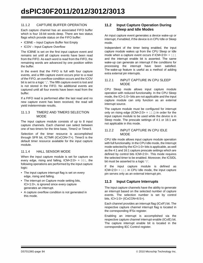
dsPIC30F2011/2012/3012/3013
11.1.2 CAPTURE BUFFER OPERATIONEach capture channel has an associated FIFO bufferwhich is four 16-bit words deep. There are two statusflags which provide status on the FIFO buffer:• ICBNE – Input Capture Buffer Not Empty• ICOV – Input Capture Overflow
The ICBNE is set on the first input capture event andremains set until all capture events have been readfrom the FIFO. As each word is read from the FIFO, theremaining words are advanced by one position withinthe buffer.
In the event that the FIFO is full with four captureevents, and a fifth capture event occurs prior to a readof the FIFO, an overflow condition occurs and the ICOVbit is set to a logic ‘1’. The fifth capture event is lost andis not stored in the FIFO. No additional events arecaptured until all four events have been read from thebuffer.
If a FIFO read is performed after the last read and nonew capture event has been received, the read willyield indeterminate results.
11.1.3 TIMER2 AND TIMER3 SELECTION MODE
The input capture module consists of up to 8 inputcapture channels. Each channel can select betweenone of two timers for the time base, Timer2 or Timer3.
Selection of the timer resource is accomplishedthrough SFR bit, ICTMR (ICxCON<7>). Timer3 is thedefault timer resource available for the input capturemodule.
11.1.4 HALL SENSOR MODEWhen the input capture module is set for capture onevery edge, rising and falling, ICM<2:0> = 001, thefollowing operations are performed by the input capturelogic:
• The input capture interrupt flag is set on every edge, rising and falling.
• The interrupt on Capture mode setting bits, ICI<1:0>, is ignored since every capture generates an interrupt.
• A capture overflow condition is not generated in this mode.
11.2 Input Capture Operation During Sleep and Idle Modes
An input capture event generates a device wake-up orinterrupt, if enabled, if the device is in CPU Idle or Sleepmode.
Independent of the timer being enabled, the inputcapture module wakes up from the CPU Sleep or Idlemode when a capture event occurs if ICM<2:0> = 111and the interrupt enable bit is asserted. The samewake-up can generate an interrupt if the conditions forprocessing the interrupt have been satisfied.The wake-up feature is useful as a method of addingextra external pin interrupts.
11.2.1 INPUT CAPTURE IN CPU SLEEP MODE
CPU Sleep mode allows input capture moduleoperation with reduced functionality. In the CPU Sleepmode, the ICI<1:0> bits are not applicable and the inputcapture module can only function as an externalinterrupt source.
The capture module must be configured for interruptonly on rising edge (ICM<2:0> = 111) in order for theinput capture module to be used while the device is inSleep mode. The prescale settings of 4:1 or 16:1 arenot applicable in this mode.
11.2.2 INPUT CAPTURE IN CPU IDLE MODE
CPU Idle mode allows input capture module operationwith full functionality. In the CPU Idle mode, the Interruptmode selected by the ICI<1:0> bits is applicable, as wellas the 4:1 and 16:1 capture prescale settings which aredefined by control bits ICM<2:0>. This mode requiresthe selected timer to be enabled. Moreover, the ICSIDLbit must be asserted to a logic ‘0’.
If the input capture module is defined asICM<2:0> = 111 in CPU Idle mode, the input capturepin serves only as an external interrupt pin.
11.3 Input Capture InterruptsThe input capture channels have the ability to generatean interrupt based on the selected number of captureevents. The selection number is set by controlbits, ICI<1:0> (ICxCON<6:5>).
Each channel provides an interrupt flag (ICxIF) bit. Therespective capture channel interrupt flag is located inthe corresponding IFSx register.
Enabling an interrupt is accomplished via therespective capture channel interrupt enable (ICxIE) bit.The capture interrupt enable bit is located in thecorresponding IEC Control register.
DS70139G-page 84 © 2010 Microchip Technology Inc.
© 2010 M
icrochip Technology Inc.D
S70139G
-page 85
dsPIC30F2011/2012/3012/3013
TAS t 2 Bit 1 Bit 0 Reset State
IC uuuu uuuu uuuu uuuu
IC ICM<2:0> 0000 0000 0000 0000
IC uuuu uuuu uuuu uuuu
IC ICM<2:0> 0000 0000 0000 0000
LeNo
BLE 11-1: INPUT CAPTURE REGISTER MAPFR Name Addr. Bit 15 Bit 14 Bit 13 Bit 12 Bit 11 Bit 10 Bit 9 Bit 8 Bit 7 Bit 6 Bit 5 Bit 4 Bit 3 Bi
1BUF 0140 Input 1 Capture Register
1CON 0142 — — ICSIDL — — — — — ICTMR ICI<1:0> ICOV ICBNE
2BUF 0144 Input 2 Capture Register
2CON 0146 — — ICSIDL — — — — — ICTMR ICI<1:0> ICOV ICBNE
gend: u = uninitialized bit; — = unimplemented bit, read as ‘0’te: Refer to the “dsPIC30F Family Reference Manual” (DS70046) for descriptions of register bit fields.

dsPIC30F2011/2012/3012/3013
NOTES:DS70139G-page 86 © 2010 Microchip Technology Inc.
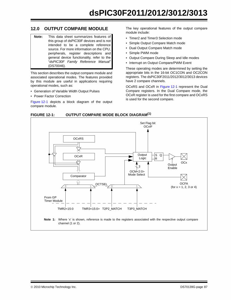
dsPIC30F2011/2012/3012/3013
12.0 OUTPUT COMPARE MODULE
This section describes the output compare module andassociated operational modes. The features providedby this module are useful in applications requiringoperational modes, such as:
• Generation of Variable Width Output Pulses• Power Factor Correction
Figure 12-1 depicts a block diagram of the outputcompare module.
The key operational features of the output comparemodule include:
• Timer2 and Timer3 Selection mode• Simple Output Compare Match mode• Dual Output Compare Match mode• Simple PWM mode• Output Compare During Sleep and Idle modes• Interrupt on Output Compare/PWM Event
These operating modes are determined by setting theappropriate bits in the 16-bit OC1CON and OC2CONregisters. The dsPIC30F2011/2012/3012/3013 deviceshave 2 compare channels.
OCxRS and OCxR in Figure 12-1 represent the DualCompare registers. In the Dual Compare mode, theOCxR register is used for the first compare and OCxRSis used for the second compare.
FIGURE 12-1: OUTPUT COMPARE MODE BLOCK DIAGRAM(1)
Note: This data sheet summarizes features ofthis group of dsPIC30F devices and is notintended to be a complete referencesource. For more information on the CPU,peripherals, register descriptions andgeneral device functionality, refer to the“dsPIC30F Family Reference Manual”(DS70046).
OCxR
Comparator
OutputLogic
QSR
OCM<2:0>
OutputOCx
Set Flag bitOCxIF
OCxRS
Mode Select
3
Note 1: Where ‘x’ is shown, reference is made to the registers associated with the respective output comparechannel (1 or 2).
OCFA OCTSEL
0 1
T2P2_MATCHTMR2<15:0 TMR3<15:0> T3P3_MATCH
From GP
(for x = 1, 2, 3 or 4)0 1
Timer Module
Enable
© 2010 Microchip Technology Inc. DS70139G-page 87
dsPIC30F2011/2012/3012/3013
12.1 Timer2 and Timer3 Selection ModeEach output compare channel can select between oneof two 16-bit timers, Timer2 or Timer3.The selection of the timers is controlled by the OCTSELbit (OCxCON<3>). Timer2 is the default timer resourcefor the output compare module.
12.2 Simple Output Compare Match Mode
When control bits OCM<2:0> (OCxCON<2:0>) = 001,010 or 011, the selected output compare channel isconfigured for one of three simple Output CompareMatch modes:
• Compare forces I/O pin low• Compare forces I/O pin high• Compare toggles I/O pin
The OCxR register is used in these modes. The OCxRregister is loaded with a value and is compared to theselected incrementing timer count. When a compareoccurs, one of these Compare Match modes occurs. Ifthe counter resets to zero before reaching the value inOCxR, the state of the OCx pin remains unchanged.
12.3 Dual Output Compare Match ModeWhen control bits OCM<2:0> (OCxCON<2:0>) = 100or 101, the selected output compare channel isconfigured for one of two Dual Output Compare modes,which are:
• Single Output Pulse mode• Continuous Output Pulse mode
12.3.1 SINGLE PULSE MODEFor the user to configure the module for the generationof a single output pulse, the following steps arerequired (assuming timer is off):
• Determine instruction cycle time TCY.• Calculate desired pulse width value based on TCY.• Calculate time to start pulse from timer start value
of 0x0000.• Write pulse width start and stop times into OCxR
and OCxRS Compare registers (x denotes channel 1 to N).
• Set Timer Period register to value equal to or greater than value in OCxRS Compare register.
• Set OCM<2:0> = 100.• Enable timer, TON bit (TxCON<15>) = 1.
To initiate another single pulse, issue another write toset OCM<2:0> = 100.
12.3.2 CONTINUOUS PULSE MODEFor the user to configure the module for the generationof a continuous stream of output pulses, the followingsteps are required:
• Determine instruction cycle time TCY.• Calculate desired pulse value based on TCY.• Calculate timer to start pulse width from timer start
value of 0x0000.• Write pulse width start and stop times into OCxR
and OCxRS (x denotes channel 1 to N) Compare registers, respectively.
• Set Timer Period register to value equal to or greater than value in OCxRS Compare register.
• Set OCM<2:0> = 101.• Enable timer, TON bit (TxCON<15>) = 1.
12.4 Simple PWM ModeWhen control bits OCM<2:0> (OCxCON<2:0>) = 110or 111, the selected output compare channel isconfigured for the PWM mode of operation. Whenconfigured for the PWM mode of operation, OCxR isthe main latch (read-only) and OCxRS is the secondarylatch. This enables glitchless PWM transitions.
The user must perform the following steps in order toconfigure the output compare module for PWMoperation:
1. Set the PWM period by writing to the appropriateperiod register.
2. Set the PWM duty cycle by writing to the OCxRSregister.
3. Configure the output compare module for PWMoperation.
4. Set the TMRx prescale value and enable theTimer, TON bit (TxCON<15>) = 1.
12.4.1 INPUT PIN FAULT PROTECTION FOR PWM
When control bits OCM<2:0> (OCxCON<2:0>) = 111,the selected output compare channel is againconfigured for the PWM mode of operation with theadditional feature of input Fault protection. While in thismode, if a logic ‘0’ is detected on the OCFA/B pin, therespective PWM output pin is placed in the highimpedance input state. The OCFLT bit (OCxCON<4>)indicates whether a Fault condition has occurred. Thisstate is maintained until both of the following eventshave occurred:
• The external Fault condition has been removed. • The PWM mode has been re-enabled by writing
to the appropriate control bits.
DS70139G-page 88 © 2010 Microchip Technology Inc.
dsPIC30F2011/2012/3012/3013
12.4.2 PWM PERIODThe PWM period is specified by writing to the PRxregister. The PWM period can be calculated usingEquation 12-1.EQUATION 12-1:
PWM frequency is defined as 1/[PWM period].
When the selected TMRx is equal to its respectiveperiod register, PRx, the following four events occur onthe next increment cycle:
• TMRx is cleared.• The OCx pin is set.
- Exception 1: If PWM duty cycle is 0x0000, the OCx pin remains low.
- Exception 2: If duty cycle is greater than PRx, the pin remains high.
• The PWM duty cycle is latched from OCxRS into OCxR.
• The corresponding timer interrupt flag is set.
See Figure 12-2 for key PWM period comparisons.Timer3 is referred to in Figure 12-2 for clarity.
FIGURE 12-2: PWM OUTPUT TIMING
PWM period = [(PRx) + 1] • 4 • Tosc •(TMRx prescale value)
Period
Duty Cycle
TMR3 = Duty Cycle TMR3 = Duty Cycle
TMR3 = PR3T3IF = 1
(Interrupt Flag)OCxR = OCxRS
TMR3 = PR3
(Interrupt Flag)OCxR = OCxRS
T3IF = 1
(OCxR) (OCxR)
© 2010 Microchip Technology Inc. DS70139G-page 89
dsPIC30F2011/2012/3012/3013
12.5 Output Compare Operation DuringCPU Sleep ModeWhen the CPU enters Sleep mode, all internal clocksare stopped. Therefore, when the CPU enters theSleep state, the output compare channel drives the pinto the active state that was observed prior to enteringthe CPU Sleep state.
For example, if the pin was high when the CPU enteredthe Sleep state, the pin remains high. Likewise, if thepin was low when the CPU entered the Sleep state, thepin remains low. In either case, the output comparemodule resumes operation when the device wakes up.
12.6 Output Compare Operation During CPU Idle Mode
When the CPU enters the Idle mode, the outputcompare module can operate with full functionality.
The output compare channel operates during the CPUIdle mode if the OCSIDL bit (OCxCON<13>) is at logic‘0’ and the selected time base (Timer2 or Timer3) isenabled and the TSIDL bit of the selected timer is setto logic ‘0’.
12.7 Output Compare InterruptsThe output compare channels have the ability togenerate an interrupt on a compare match, forwhichever Match mode has been selected.
For all modes except the PWM mode, when a compareevent occurs, the respective interrupt flag (OCxIF) isasserted and an interrupt is generated if enabled. TheOCxIF bit is located in the corresponding IFS registerand must be cleared in software. The interrupt isenabled via the respective compare interrupt enable(OCxIE) bit located in the corresponding IEC Controlregister.
For the PWM mode, when an event occurs, therespective timer interrupt flag (T2IF or T3IF) is assertedand an interrupt is generated if enabled. The IF bit islocated in the IFS0 register and must be cleared insoftware. The interrupt is enabled via the respectivetimer interrupt enable bit (T2IE or T3IE) located in theIEC0 Control register. The output compare interruptflag is never set during the PWM mode of operation.
DS70139G-page 90 © 2010 Microchip Technology Inc.
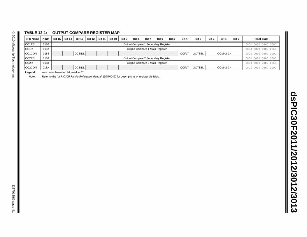
© 2010 M
icrochip Technology Inc.D
S70139G
-page 91
dsPIC30F2011/2012/3012/3013
TASF Bit 1 Bit 0 Reset State
OC 0000 0000 0000 0000
OC 0000 0000 0000 0000
OC OCM<2:0> 0000 0000 0000 0000
OC 0000 0000 0000 0000
OC 0000 0000 0000 0000
OC OCM<2:0> 0000 0000 0000 0000
Le
BLE 12-1: OUTPUT COMPARE REGISTER MAPR Name Addr. Bit 15 Bit 14 Bit 13 Bit 12 Bit 11 Bit 10 Bit 9 Bit 8 Bit 7 Bit 6 Bit 5 Bit 4 Bit 3 Bit 2
1RS 0180 Output Compare 1 Secondary Register
1R 0182 Output Compare 1 Main Register
1CON 0184 — — OCSIDL — — — — — — — — OCFLT OCTSEL
2RS 0186 Output Compare 2 Secondary Register
2R 0188 Output Compare 2 Main Register
2CON 018A — — OCSIDL — — — — — — — — OCFLT OCTSEL
gend: — = unimplemented bit, read as ‘0’Note: Refer to the “dsPIC30F Family Reference Manual” (DS70046) for descriptions of register bit fields.

dsPIC30F2011/2012/3012/3013
NOTES:DS70139G-page 92 © 2010 Microchip Technology Inc.
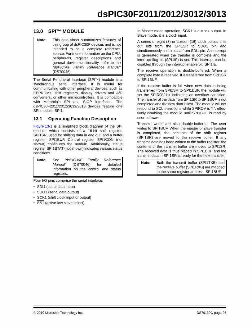
dsPIC30F2011/2012/3012/3013
13.0 SPI™ MODULE
The Serial Peripheral Interface (SPI™) module is asynchronous serial interface. It is useful forcommunicating with other peripheral devices, such asEEPROMs, shift registers, display drivers and A/Dconverters, or other microcontrollers. It is compatiblewith Motorola's SPI and SIOP interfaces. ThedsPIC30F2011/2012/3012/3013 devices feature oneSPI module, SPI1.
13.1 Operating Function DescriptionFigure 13-1 is a simplified block diagram of the SPImodule, which consists of a 16-bit shift register,SPI1SR, used for shifting data in and out, and a bufferregister, SPI1BUF. Control register SPI1CON (notshown) configures the module. Additionally, statusregister SPI1STAT (not shown) indicates various statusconditions.
Four I/O pins comprise the serial interface:
• SDI1 (serial data input)• SDO1 (serial data output)• SCK1 (shift clock input or output)• SS1 (active-low slave select).
In Master mode operation, SCK1 is a clock output. InSlave mode, it is a clock input.
A series of eight (8) or sixteen (16) clock pulses shiftout bits from the SPI1SR to SDO1 pin andsimultaneously shift in data from SDI1 pin. An interruptis generated when the transfer is complete and theinterrupt flag bit (SPI1IF) is set. This interrupt can bedisabled through the interrupt enable bit, SPI1IE.
The receive operation is double-buffered. When acomplete byte is received, it is transferred from SPI1SRto SPI1BUF.
If the receive buffer is full when new data is beingtransferred from SPI1SR to SPI1BUF, the module willset the SPIROV bit indicating an overflow condition.The transfer of the data from SPI1SR to SPI1BUF is notcompleted and the new data is lost. The module will notrespond to SCL transitions while SPIROV is ‘1’, effec-tively disabling the module until SPI1BUF is read byuser software.
Transmit writes are also double-buffered. The userwrites to SPI1BUF. When the master or slave transferis completed, the contents of the shift register(SPI1SR) are moved to the receive buffer. If anytransmit data has been written to the buffer register, thecontents of the transmit buffer are moved to SPI1SR.The received data is thus placed in SPI1BUF and thetransmit data in SPI1SR is ready for the next transfer.
Note: This data sheet summarizes features ofthis group of dsPIC30F devices and is notintended to be a complete referencesource. For more information on the CPU,peripherals, register descriptions andgeneral device functionality, refer to the“dsPIC30F Family Reference Manual”(DS70046).
Note: See “dsPIC30F Family ReferenceManual” (DS70046) for detailedinformation on the control and statusregisters.
Note: Both the transmit buffer (SPI1TXB) andthe receive buffer (SPI1RXB) are mappedto the same register address, SPI1BUF.
© 2010 Microchip Technology Inc. DS70139G-page 93
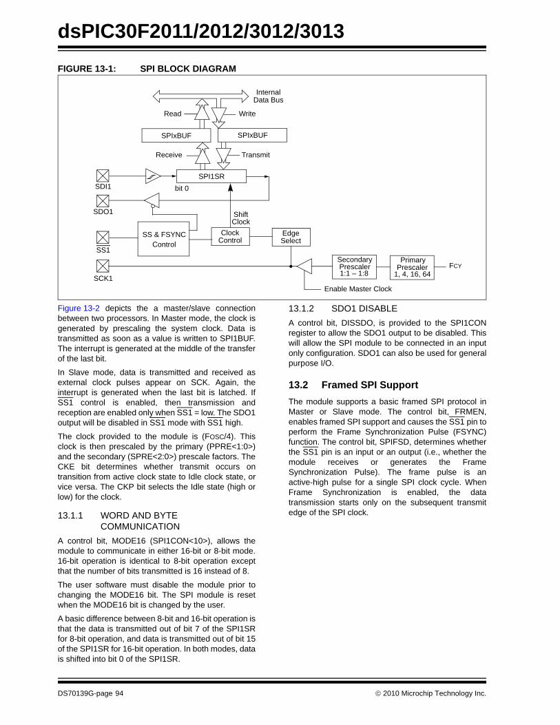
dsPIC30F2011/2012/3012/3013
FIGURE 13-1: SPI BLOCK DIAGRAMFigure 13-2 depicts the a master/slave connectionbetween two processors. In Master mode, the clock isgenerated by prescaling the system clock. Data istransmitted as soon as a value is written to SPI1BUF.The interrupt is generated at the middle of the transferof the last bit.
In Slave mode, data is transmitted and received asexternal clock pulses appear on SCK. Again, theinterrupt is generated when the last bit is latched. IfSS1 control is enabled, then transmission andreception are enabled only when SS1 = low. The SDO1output will be disabled in SS1 mode with SS1 high.
The clock provided to the module is (FOSC/4). Thisclock is then prescaled by the primary (PPRE<1:0>)and the secondary (SPRE<2:0>) prescale factors. TheCKE bit determines whether transmit occurs ontransition from active clock state to Idle clock state, orvice versa. The CKP bit selects the Idle state (high orlow) for the clock.
13.1.1 WORD AND BYTE COMMUNICATION
A control bit, MODE16 (SPI1CON<10>), allows themodule to communicate in either 16-bit or 8-bit mode.16-bit operation is identical to 8-bit operation exceptthat the number of bits transmitted is 16 instead of 8.
The user software must disable the module prior tochanging the MODE16 bit. The SPI module is resetwhen the MODE16 bit is changed by the user.
A basic difference between 8-bit and 16-bit operation isthat the data is transmitted out of bit 7 of the SPI1SRfor 8-bit operation, and data is transmitted out of bit 15of the SPI1SR for 16-bit operation. In both modes, datais shifted into bit 0 of the SPI1SR.
13.1.2 SDO1 DISABLEA control bit, DISSDO, is provided to the SPI1CONregister to allow the SDO1 output to be disabled. Thiswill allow the SPI module to be connected in an inputonly configuration. SDO1 can also be used for generalpurpose I/O.
13.2 Framed SPI SupportThe module supports a basic framed SPI protocol inMaster or Slave mode. The control bit, FRMEN,enables framed SPI support and causes the SS1 pin toperform the Frame Synchronization Pulse (FSYNC)function. The control bit, SPIFSD, determines whetherthe SS1 pin is an input or an output (i.e., whether themodule receives or generates the FrameSynchronization Pulse). The frame pulse is anactive-high pulse for a single SPI clock cycle. WhenFrame Synchronization is enabled, the datatransmission starts only on the subsequent transmitedge of the SPI clock.
Read Write
InternalData Bus
SDI1
SDO1
SS1
SCK1
SPI1SR
SPIxBUF
bit 0
ShiftClock
EdgeSelect
FCYPrimary
1, 4, 16, 64
Enable Master Clock
PrescalerSecondaryPrescaler1:1 – 1:8
SS & FSYNCControl
ClockControl
Transmit
SPIxBUF
Receive
DS70139G-page 94 © 2010 Microchip Technology Inc.
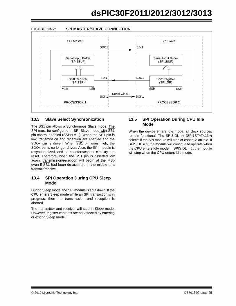
dsPIC30F2011/2012/3012/3013
FIGURE 13-2: SPI MASTER/SLAVE CONNECTION13.3 Slave Select SynchronizationThe SS1 pin allows a Synchronous Slave mode. TheSPI must be configured in SPI Slave mode with SS1pin control enabled (SSEN = 1). When the SS1 pin islow, transmission and reception are enabled and theSDOx pin is driven. When SS1 pin goes high, theSDOx pin is no longer driven. Also, the SPI module isresynchronized, and all counters/control circuitry arereset. Therefore, when the SS1 pin is asserted lowagain, transmission/reception will begin at the MSbeven if SS1 had been de-asserted in the middle of atransmit/receive.
13.4 SPI Operation During CPU Sleep Mode
During Sleep mode, the SPI module is shut down. If theCPU enters Sleep mode while an SPI transaction is inprogress, then the transmission and reception isaborted.
The transmitter and receiver will stop in Sleep mode.However, register contents are not affected by enteringor exiting Sleep mode.
13.5 SPI Operation During CPU Idle Mode
When the device enters Idle mode, all clock sourcesremain functional. The SPISIDL bit (SPI1STAT<13>)selects if the SPI module will stop or continue on idle. IfSPISIDL = 0, the module will continue to operate whenthe CPU enters Idle mode. If SPISIDL = 1, the modulewill stop when the CPU enters Idle mode.
Serial Input Buffer(SPI1BUF)
Shift Register(SPI1SR)
MSb LSb
SDO1
SDI1
PROCESSOR 1
SCK1
SPI Master
Serial Input Buffer(SPI1BUF)
Shift Register(SPI1SR)
LSbMSb
SDI1
SDO1
PROCESSOR 2
SCK1
SPI Slave
Serial Clock
© 2010 Microchip Technology Inc. DS70139G-page 95
dsPIC30F2011/2012/3012/3013
DS
70139G-page 96
© 2010 M
icrochip Technology Inc.
Bit 2 Bit 1 Bit 0 Reset State
— SPITBF SPIRBF 0000 0000 0000 0000
SPRE0 PPRE1 PPRE0 0000 0000 0000 0000
0000 0000 0000 0000
TABLE 13-1: SPI1 REGISTER MAPSFR
Name Addr. Bit 15 Bit 14 Bit 13 Bit 12 Bit 11 Bit 10 Bit 9 Bit 8 Bit 7 Bit 6 Bit 5 Bit 4 Bit 3
SPI1STAT 0220 SPIEN — SPISIDL — — — — — — SPIROV — — —
SPI1CON 0222 — FRMEN SPIFSD — DISSDO MODE16 SMP CKE SSEN CKP MSTEN SPRE2 SPRE1
SPI1BUF 0224 Transmit and Receive Buffer
Legend: — = unimplemented bit, read as ‘0’Note: Refer to the “dsPIC30F Family Reference Manual” (DS70046) for descriptions of register bit fields.
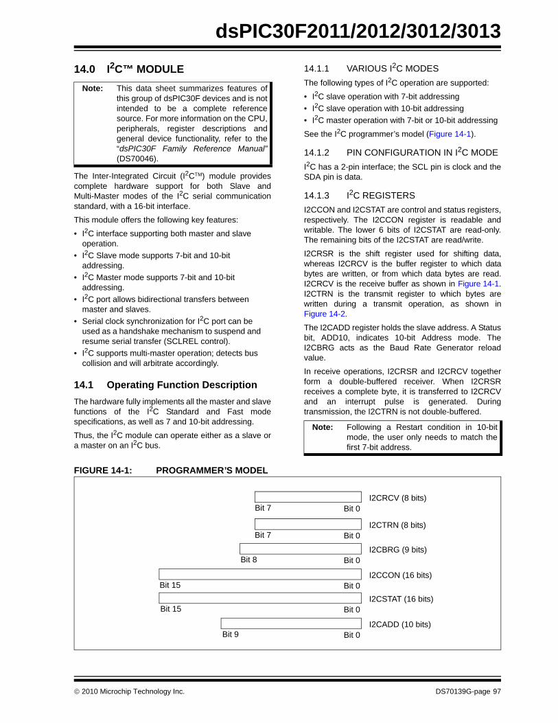
dsPIC30F2011/2012/3012/3013
14.0 I2C™ MODULE
The Inter-Integrated Circuit (I2CTM) module providescomplete hardware support for both Slave andMulti-Master modes of the I2C serial communicationstandard, with a 16-bit interface.
This module offers the following key features:
• I2C interface supporting both master and slave operation.
• I2C Slave mode supports 7-bit and 10-bit addressing.
• I2C Master mode supports 7-bit and 10-bit addressing.
• I2C port allows bidirectional transfers between master and slaves.
• Serial clock synchronization for I2C port can be used as a handshake mechanism to suspend and resume serial transfer (SCLREL control).
• I2C supports multi-master operation; detects bus collision and will arbitrate accordingly.
14.1 Operating Function DescriptionThe hardware fully implements all the master and slavefunctions of the I2C Standard and Fast modespecifications, as well as 7 and 10-bit addressing.
Thus, the I2C module can operate either as a slave ora master on an I2C bus.
14.1.1 VARIOUS I2C MODESThe following types of I2C operation are supported:
• I2C slave operation with 7-bit addressing• I2C slave operation with 10-bit addressing• I2C master operation with 7-bit or 10-bit addressing
See the I2C programmer’s model (Figure 14-1).
14.1.2 PIN CONFIGURATION IN I2C MODEI2C has a 2-pin interface; the SCL pin is clock and theSDA pin is data.
14.1.3 I2C REGISTERSI2CCON and I2CSTAT are control and status registers,respectively. The I2CCON register is readable andwritable. The lower 6 bits of I2CSTAT are read-only.The remaining bits of the I2CSTAT are read/write.
I2CRSR is the shift register used for shifting data,whereas I2CRCV is the buffer register to which databytes are written, or from which data bytes are read.I2CRCV is the receive buffer as shown in Figure 14-1.I2CTRN is the transmit register to which bytes arewritten during a transmit operation, as shown inFigure 14-2.
The I2CADD register holds the slave address. A Statusbit, ADD10, indicates 10-bit Address mode. TheI2CBRG acts as the Baud Rate Generator reloadvalue.
In receive operations, I2CRSR and I2CRCV togetherform a double-buffered receiver. When I2CRSRreceives a complete byte, it is transferred to I2CRCVand an interrupt pulse is generated. Duringtransmission, the I2CTRN is not double-buffered.
FIGURE 14-1: PROGRAMMER’S MODEL
Note: This data sheet summarizes features ofthis group of dsPIC30F devices and is notintended to be a complete referencesource. For more information on the CPU,peripherals, register descriptions andgeneral device functionality, refer to the“dsPIC30F Family Reference Manual”(DS70046).
Note: Following a Restart condition in 10-bitmode, the user only needs to match thefirst 7-bit address.
Bit 7 Bit 0I2CRCV (8 bits)
Bit 7 Bit 0I2CTRN (8 bits)
Bit 8 Bit 0I2CBRG (9 bits)
Bit 15 Bit 0I2CCON (16 bits)
Bit 15 Bit 0I2CSTAT (16 bits)
Bit 9 Bit 0I2CADD (10 bits)
© 2010 Microchip Technology Inc. DS70139G-page 97
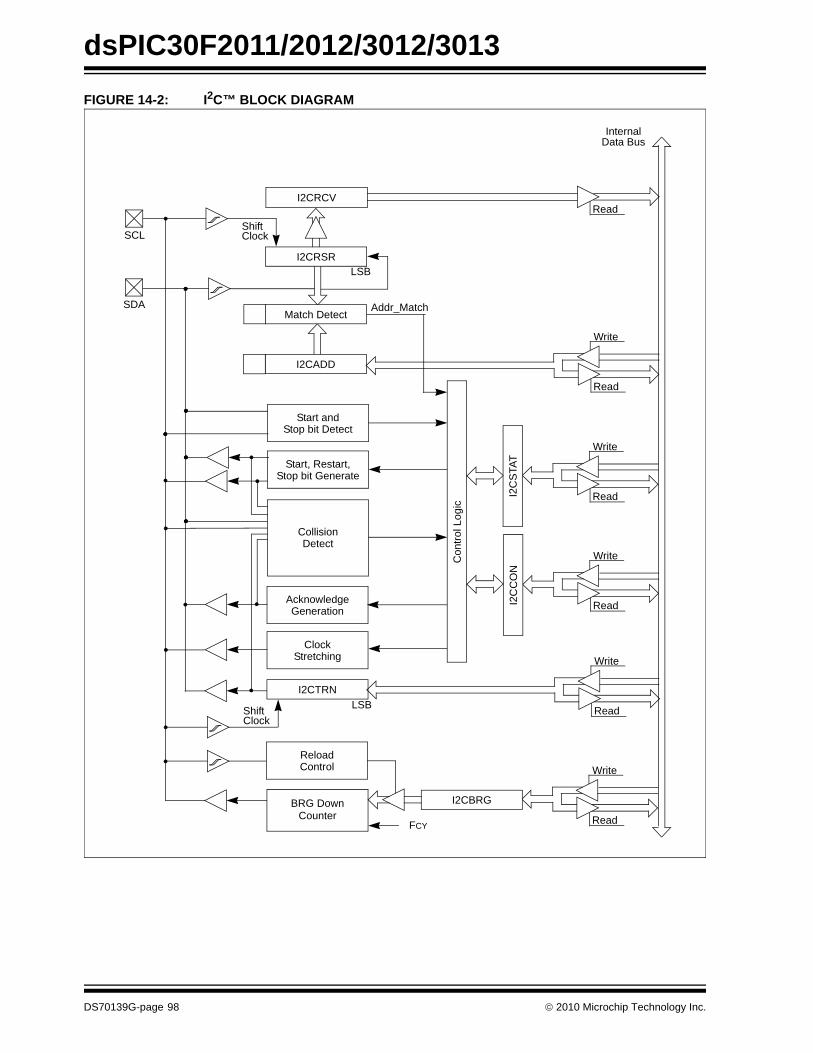
dsPIC30F2011/2012/3012/3013
FIGURE 14-2: I2C™ BLOCK DIAGRAMI2CRSR
I2CRCV
InternalData Bus
SCL
SDA
Shift
Match Detect
I2CADD
Start andStop bit Detect
Clock
Addr_Match
ClockStretching
I2CTRNLSBShift
Clock
Write
ReadBRG Down I2CBRG
ReloadControl
FCY
Start, Restart,Stop bit Generate
Write
Read
AcknowledgeGeneration
CollisionDetect
Write
Read
Write
ReadI2C
CO
N
Write
ReadI2C
STA
T
Con
trol L
ogic
Read
LSB
Counter
DS70139G-page 98 © 2010 Microchip Technology Inc.
dsPIC30F2011/2012/3012/3013
14.2 I2C Module AddressesThe I2CADD register contains the Slave modeaddresses. The register is a 10-bit register.If the A10M bit (I2CCON<10>) is ‘0’, the address isinterpreted by the module as a 7-bit address. When anaddress is received, it is compared to the 7 LSb of theI2CADD register.
If the A10M bit is ‘1’, the address is assumed to be a10-bit address. When an address is received, it will becompared with the binary value ‘11110 A9 A8’ (whereA9 and A8 are two Most Significant bits of I2CADD). Ifthat value matches, the next address will be comparedwith the Least Significant 8 bits of I2CADD, as specifiedin the 10-bit addressing protocol.
The 7-bit I2C Slave Addresses supported by thedsPIC30F are shown in Table 14-1.
TABLE 14-1: 7-BIT I2C™ SLAVE ADDRESSES
14.3 I2C 7-bit Slave Mode OperationOnce enabled (I2CEN = 1), the slave module will waitfor a Start bit to occur (i.e., the I2C module is ‘Idle’).Following the detection of a Start bit, 8 bits are shiftedinto I2CRSR and the address is compared againstI2CADD. In 7-bit mode (A10M = 0), bits I2CADD<6:0>are compared against I2CRSR<7:1> and I2CRSR<0>is the R_W bit. All incoming bits are sampled on the ris-ing edge of SCL.
If an address match occurs, an acknowledgement willbe sent, and the slave event interrupt flag (SI2CIF) isset on the falling edge of the ninth (ACK) bit. Theaddress match does not affect the contents of theI2CRCV buffer or the RBF bit.
14.3.1 SLAVE TRANSMISSIONIf the R_W bit received is a ‘1’, then the serial port willgo into Transmit mode. It will send ACK on the ninth bitand then hold SCL to ‘0’ until the CPU responds bywriting to I2CTRN. SCL is released by setting theSCLREL bit, and 8 bits of data are shifted out. Data bitsare shifted out on the falling edge of SCL, such thatSDA is valid during SCL high. The interrupt pulse issent on the falling edge of the ninth clock pulse,regardless of the status of the ACK received from themaster.
14.3.2 SLAVE RECEPTIONIf the R_W bit received is a ‘0’ during an addressmatch, then Receive mode is initiated. Incoming bitsare sampled on the rising edge of SCL. After 8 bits arereceived, if I2CRCV is not full or I2COV is not set,I2CRSR is transferred to I2CRCV. ACK is sent on theninth clock.
If the RBF flag is set, indicating that I2CRCV is stillholding data from a previous operation (RBF = 1), thenACK is not sent; however, the interrupt pulse isgenerated. In the case of an overflow, the contents ofthe I2CRSR are not loaded into the I2CRCV.
14.4 I2C 10-bit Slave Mode OperationIn 10-bit mode, the basic receive and transmitoperations are the same as in the 7-bit mode. However,the criteria for address match is more complex.
The I2C specification dictates that a slave must beaddressed for a write operation with two address bytesfollowing a Start bit.
The A10M bit is a control bit that signifies that theaddress in I2CADD is a 10-bit address rather than a 7-bitaddress. The address detection protocol for the first byteof a message address is identical for 7-bit and 10-bitmessages, but the bits being compared are different.
I2CADD holds the entire 10-bit address. Uponreceiving an address following a Start bit, I2CRSR<7:3> is compared against a literal ‘11110’ (the default10-bit address) and I2CRSR<2:1> are comparedagainst I2CADD<9:8>. If a match occurs and ifR_W = 0, the interrupt pulse is sent. The ADD10 bit willbe cleared to indicate a partial address match. If amatch fails or R_W = 1, the ADD10 bit is cleared andthe module returns to the Idle state.
The low byte of the address is then received andcompared with I2CADD<7:0>. If an address matchoccurs, the interrupt pulse is generated and the ADD10bit is set, indicating a complete 10-bit address match. Ifan address match did not occur, the ADD10 bit iscleared and the module returns to the Idle state.
0x00 General call address or start byte0x01-0x03 Reserved0x04-0x07 Hs-mode Master codes0x04-0x77 Valid 7-bit addresses0x78-0x7b Valid 10-bit addresses (lower 7
bits)0x7c-0x7f Reserved
Note: The I2CRCV will be loaded if the I2COVbit = 1 and the RBF flag = 0. In this case,a read of the I2CRCV was performed butthe user did not clear the state of theI2COV bit before the next receiveoccurred. The acknowledgement is notsent (ACK = 1) and the I2CRCV isupdated.
© 2010 Microchip Technology Inc. DS70139G-page 99
dsPIC30F2011/2012/3012/3013
14.4.1 10-BIT MODE SLAVETRANSMISSIONOnce a slave is addressed in this fashion with the full10-bit address (we will refer to this state as“PRIOR_ADDR_MATCH”), the master can beginsending data bytes for a slave reception operation.
14.4.2 10-BIT MODE SLAVE RECEPTIONOnce addressed, the master can generate a RepeatedStart, reset the high byte of the address and set theR_W bit without generating a Stop bit, thus initiating aslave transmit operation.
14.5 Automatic Clock StretchIn the Slave modes, the module can synchronize bufferreads and write to the master device by clock stretching.
14.5.1 TRANSMIT CLOCK STRETCHINGBoth 10-bit and 7-bit Transmit modes implement clockstretching by asserting the SCLREL bit after the fallingedge of the ninth clock, if the TBF bit is cleared,indicating the buffer is empty.
In Slave Transmit modes, clock stretching is alwaysperformed irrespective of the STREN bit.
Clock synchronization takes place following the ninthclock of the transmit sequence. If the device samplesan ACK on the falling edge of the ninth clock and if theTBF bit is still clear, then the SCLREL bit isautomatically cleared. The SCLREL being cleared to‘0’ will assert the SCL line low. The user’s ISR must setthe SCLREL bit before transmission is allowed tocontinue. By holding the SCL line low, the user has timeto service the ISR and load the contents of the I2CTRNbefore the master device can initiate another transmitsequence.
14.5.2 RECEIVE CLOCK STRETCHINGThe STREN bit in the I2CCON register can be used toenable clock stretching in Slave Receive mode. Whenthe STREN bit is set, the SCL pin will be held low at theend of each data receive sequence.
14.5.3 CLOCK STRETCHING DURING 7-BIT ADDRESSING (STREN = 1)
When the STREN bit is set in Slave Receive mode, theSCL line is held low when the buffer register is full. Themethod for stretching the SCL output is the same forboth 7 and 10-bit addressing modes.
Clock stretching takes place following the ninth clock ofthe receive sequence. On the falling edge of the ninthclock at the end of the ACK sequence, if the RBF bit isset, the SCLREL bit is automatically cleared, forcingthe SCL output to be held low. The user’s ISR must setthe SCLREL bit before reception is allowed to continue.By holding the SCL line low, the user has time toservice the ISR and read the contents of the I2CRCVbefore the master device can initiate another receivesequence. This will prevent buffer overruns fromoccurring.
14.5.4 CLOCK STRETCHING DURING 10-BIT ADDRESSING (STREN = 1)
Clock stretching takes place automatically during theaddressing sequence. Because this module has aregister for the entire address, it is not necessary forthe protocol to wait for the address to be updated.
After the address phase is complete, clock stretchingwill occur on each data receive or transmit sequence aswas described earlier.
14.6 Software Controlled Clock Stretching (STREN = 1)
When the STREN bit is ‘1’, the SCLREL bit may becleared by software to allow software to control theclock stretching. The logic will synchronize writes to theSCLREL bit with the SCL clock. Clearing the SCLRELbit will not assert the SCL output until the moduledetects a falling edge on the SCL output and SCL issampled low. If the SCLREL bit is cleared by the userwhile the SCL line has been sampled low, the SCLoutput will be asserted (held low). The SCL output willremain low until the SCLREL bit is set, and all otherdevices on the I2C bus have de-asserted SCL. Thisensures that a write to the SCLREL bit will not violatethe minimum high time requirement for SCL.
If the STREN bit is ‘0’, a software write to the SCLRELbit will be disregarded and have no effect on theSCLREL bit.
Note 1: If the user loads the contents of I2CTRN,setting the TBF bit before the falling edgeof the ninth clock, the SCLREL bit will notbe cleared and clock stretching will notoccur.
2: The SCLREL bit can be set in software,regardless of the state of the TBF bit.
Note 1: If the user reads the contents of theI2CRCV, clearing the RBF bit before thefalling edge of the ninth clock, theSCLREL bit will not be cleared and clockstretching will not occur.
2: The SCLREL bit can be set in softwareregardless of the state of the RBF bit. Theuser should be careful to clear the RBFbit in the ISR before the next receivesequence in order to prevent an overflowcondition.
DS70139G-page 100 © 2010 Microchip Technology Inc.
dsPIC30F2011/2012/3012/3013
14.7 InterruptsThe I2C module generates two interrupt flags, MI2CIF(I2C Master Interrupt Flag) and SI2CIF (I2C SlaveInterrupt Flag). The MI2CIF interrupt flag is activatedon completion of a master message event. The SI2CIFinterrupt flag is activated on detection of a messagedirected to the slave.14.8 Slope ControlThe I2C standard requires slope control on the SDAand SCL signals for Fast mode (400 kHz). The controlbit, DISSLW, enables the user to disable slew ratecontrol if desired. It is necessary to disable the slewrate control for 1 MHz mode.
14.9 IPMI SupportThe control bit, IPMIEN, enables the module to supportIntelligent Peripheral Management Interface (IPMI).When this bit is set, the module accepts and acts uponall addresses.
14.10 General Call Address SupportThe general call address can address all devices.When this address is used, all devices should, intheory, respond with an acknowledgement.
The general call address is one of eight addressesreserved for specific purposes by the I2C protocol. Itconsists of all ‘0’s with R_W = 0.
The general call address is recognized when theGeneral Call Enable (GCEN) bit is set(I2CCON<7> = 1). Following a Start bit detection, 8 bitsare shifted into I2CRSR and the address is comparedwith I2CADD, and is also compared with the generalcall address which is fixed in hardware.
If a general call address match occurs, the I2CRSR istransferred to the I2CRCV after the eighth clock, the RBFflag is set and on the falling edge of the ninth bit (ACKbit), the master event interrupt flag (MI2CIF) is set.
When the interrupt is serviced, the source for theinterrupt can be checked by reading the contents of theI2CRCV to determine if the address was devicespecific or a general call address.
14.11 I2C Master SupportAs a master device, six operations are supported:
• Assert a Start condition on SDA and SCL.• Assert a Restart condition on SDA and SCL.• Write to the I2CTRN register initiating
transmission of data/address.• Generate a Stop condition on SDA and SCL.• Configure the I2C port to receive data.• Generate an ACK condition at the end of a
received byte of data.
14.12 I2C Master OperationThe master device generates all of the serial clockpulses and the Start and Stop conditions. A transfer isended with a Stop condition or with a Repeated Startcondition. Since the Repeated Start condition is alsothe beginning of the next serial transfer, the I2C bus willnot be released.
In Master Transmitter mode, serial data is outputthrough SDA, while SCL outputs the serial clock. Thefirst byte transmitted contains the slave address of thereceiving device (7 bits) and the data direction bit. Inthis case, the data direction bit (R_W) is logic ‘0’. Serialdata is transmitted 8 bits at a time. After each byte istransmitted, an ACK bit is received. Start and Stopconditions are output to indicate the beginning and theend of a serial transfer.
In Master Receive mode, the first byte transmittedcontains the slave address of the transmitting device(7 bits) and the data direction bit. In this case, the datadirection bit (R_W) is logic ‘1’. Thus, the first bytetransmitted is a 7-bit slave address, followed by a ‘1’ toindicate receive bit. Serial data is received via SDAwhile SCL outputs the serial clock. Serial data isreceived 8 bits at a time. After each byte is received, anACK bit is transmitted. Start and Stop conditionsindicate the beginning and end of transmission.
14.12.1 I2C MASTER TRANSMISSIONTransmission of a data byte, a 7-bit address, or the sec-ond half of a 10-bit address, is accomplished by simplywriting a value to I2CTRN register. The user shouldonly write to I2CTRN when the module is in a WAITstate. This action will set the Buffer Full Flag (TBF) andallow the Baud Rate Generator to begin counting andstart the next transmission. Each bit of address/datawill be shifted out onto the SDA pin after the fallingedge of SCL is asserted. The Transmit Status Flag,TRSTAT (I2CSTAT<14>), indicates that a mastertransmit is in progress.
© 2010 Microchip Technology Inc. DS70139G-page 101
dsPIC30F2011/2012/3012/3013
14.12.2 I2C MASTER RECEPTIONMaster mode reception is enabled by programming theReceive Enable bit, RCEN (I2CCON<3>). The I2Cmodule must be Idle before the RCEN bit is set,otherwise the RCEN bit will be disregarded. The BaudRate Generator begins counting and on each rollover,the state of the SCL pin ACK and data are shifted intothe I2CRSR on the rising edge of each clock.14.12.3 BAUD RATE GENERATOR In I2C Master mode, the reload value for the BRG islocated in the I2CBRG register. When the BRG isloaded with this value, the BRG counts down to ‘0’ andstops until another reload has taken place. If clockarbitration is taking place, for instance, the BRG isreloaded when the SCL pin is sampled high.
As per the I2C standard, FSCK may be 100 kHz or400 kHz. However, the user can specify any baud rateup to 1 MHz. I2CBRG values of ‘0’ or ‘1’ are illegal.
EQUATION 14-1: SERIAL CLOCK RATE
14.12.4 CLOCK ARBITRATIONClock arbitration occurs when the master de-assertsthe SCL pin (SCL allowed to float high) during anyreceive, transmit, or Restart/Stop condition. When theSCL pin is allowed to float high, the Baud RateGenerator (BRG) is suspended from counting until theSCL pin is actually sampled high. When the SCL pin issampled high, the Baud Rate Generator is reloadedwith the contents of I2CBRG and begins counting. Thisensures that the SCL high time will always be at leastone BRG rollover count in the event that the clock isheld low by an external device.
14.12.5 MULTI-MASTER COMMUNICATION, BUS COLLISION, AND BUS ARBITRATION
Multi-master operation support is achieved by busarbitration. When the master outputs address/data bitsonto the SDA pin, arbitration takes place when themaster outputs a ‘1’ on SDA by letting SDA float highwhile another master asserts a ‘0’. When the SCL pinfloats high, data should be stable. If the expected dataon SDA is a ‘1’ and the data sampled on the SDApin = 0, then a bus collision has taken place. Themaster will set the MI2CIF pulse and reset the masterportion of the I2C port to its Idle state.
If a transmit was in progress when the bus collisionoccurred, the transmission is halted, the TBF flag iscleared, the SDA and SCL lines are de-asserted and avalue can now be written to I2CTRN. When the userservices the I2C master event Interrupt ServiceRoutine, if the I2C bus is free (i.e., the P bit is set), theuser can resume communication by asserting a Startcondition.
If a Start, Restart, Stop or Acknowledge condition wasin progress when the bus collision occurred, thecondition is aborted, the SDA and SCL lines arede-asserted, and the respective control bits in theI2CCON register are cleared to ‘0’. When the userservices the bus collision Interrupt Service Routine,and if the I2C bus is free, the user can resumecommunication by asserting a Start condition.
The master will continue to monitor the SDA and SCLpins, and if a Stop condition occurs, the MI2CIF bit willbe set.
A write to the I2CTRN will start the transmission of dataat the first data bit regardless of where the transmitterleft off when bus collision occurred.
In a multi-master environment, the interrupt generationon the detection of Start and Stop conditions allows thedetermination of when the bus is free. Control of the I2Cbus can be taken when the P bit is set in the I2CSTATregister, or the bus is Idle and the S and P bits arecleared.
14.13 I2C Module Operation During CPU Sleep and Idle Modes
14.13.1 I2C OPERATION DURING CPU SLEEP MODE
When the device enters Sleep mode, all clock sourcesto the module are shut down and stay at logic ‘0’. IfSleep occurs in the middle of a transmission and thestate machine is partially into a transmission as theclocks stop, then the transmission is aborted. Similarly,if Sleep occurs in the middle of a reception, then thereception is aborted.
14.13.2 I2C OPERATION DURING CPU IDLE MODE
For the I2C, the I2CSIDL bit selects if the module willstop on Idle or continue on Idle. If I2CSIDL = 0, themodule will continue operation on assertion of the Idlemode. If I2CSIDL = 1, the module will stop on Idle.
I2CBRG = FCY FCYFSCL 1,111,111
– 1–( )
DS70139G-page 102 © 2010 Microchip Technology Inc.
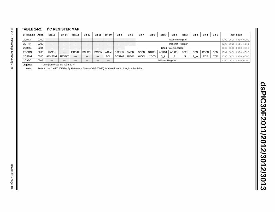
© 2010 M
icrochip Technology Inc.D
S70139G
-page 103
dsPIC30F2011/2012/3012/3013
TASF it 2 Bit 1 Bit 0 Reset State
I2C 0000 0000 0000 0000
I2C 0000 0000 1111 1111
I2C 0000 0000 0000 0000
I2C EN RSEN SEN 0001 0000 0000 0000
I2C _W RBF TBF 0000 0000 0000 0000
I2C 0000 0000 0000 0000
Le
BLE 14-2: I2C REGISTER MAPR Name Addr. Bit 15 Bit 14 Bit 13 Bit 12 Bit 11 Bit 10 Bit 9 Bit 8 Bit 7 Bit 6 Bit 5 Bit 4 Bit 3 B
RCV 0200 — — — — — — — — Receive Register
TRN 0202 — — — — — — — — Transmit Register
BRG 0204 — — — — — — — Baud Rate Generator
CON 0206 I2CEN — I2CSIDL SCLREL IPMIEN A10M DISSLW SMEN GCEN STREN ACKDT ACKEN RCEN P
STAT 0208 ACKSTAT TRSTAT — — — BCL GCSTAT ADD10 IWCOL I2COV D_A P S R
ADD 020A — — — — — — Address Register
gend: — = unimplemented bit, read as ‘0’Note: Refer to the “dsPIC30F Family Reference Manual” (DS70046) for descriptions of register bit fields.

dsPIC30F2011/2012/3012/3013
NOTES:DS70139G-page 104 © 2010 Microchip Technology Inc.
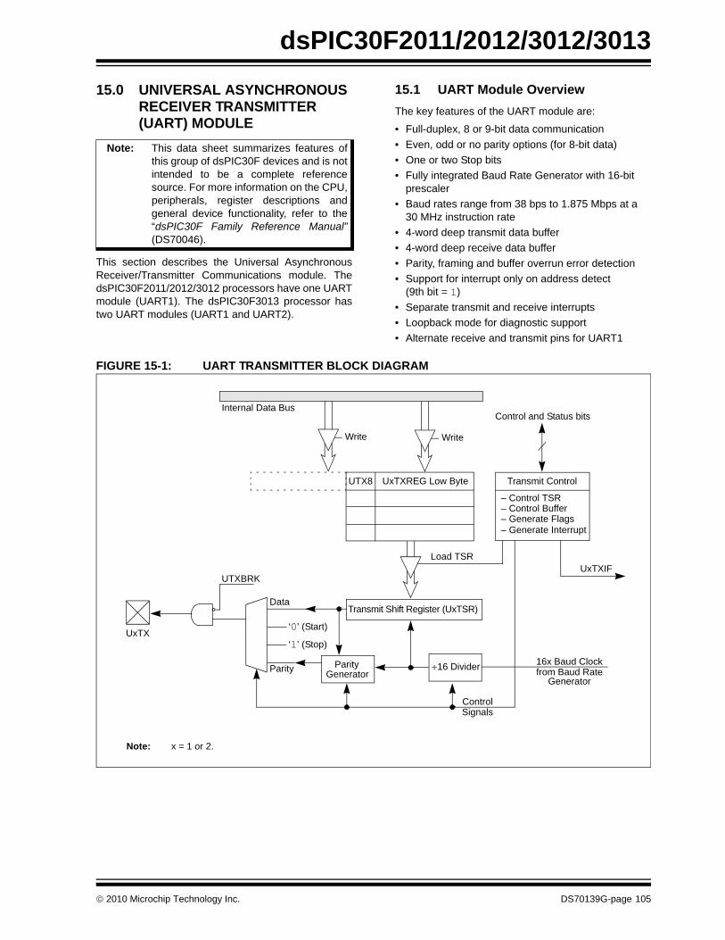
dsPIC30F2011/2012/3012/3013
15.0 UNIVERSAL ASYNCHRONOUS RECEIVER TRANSMITTER (UART) MODULE
This section describes the Universal AsynchronousReceiver/Transmitter Communications module. ThedsPIC30F2011/2012/3012 processors have one UARTmodule (UART1). The dsPIC30F3013 processor hastwo UART modules (UART1 and UART2).
15.1 UART Module OverviewThe key features of the UART module are:
• Full-duplex, 8 or 9-bit data communication• Even, odd or no parity options (for 8-bit data)• One or two Stop bits• Fully integrated Baud Rate Generator with 16-bit
prescaler• Baud rates range from 38 bps to 1.875 Mbps at a
30 MHz instruction rate• 4-word deep transmit data buffer• 4-word deep receive data buffer• Parity, framing and buffer overrun error detection• Support for interrupt only on address detect
(9th bit = 1)• Separate transmit and receive interrupts• Loopback mode for diagnostic support• Alternate receive and transmit pins for UART1
FIGURE 15-1: UART TRANSMITTER BLOCK DIAGRAM
Note: This data sheet summarizes features ofthis group of dsPIC30F devices and is notintended to be a complete referencesource. For more information on the CPU,peripherals, register descriptions andgeneral device functionality, refer to the“dsPIC30F Family Reference Manual”(DS70046).
Write Write
UTX8 UxTXREG Low Byte
Load TSR
Transmit Control
– Control TSR– Control Buffer– Generate Flags– Generate Interrupt
Control and Status bits
UxTXIF
Data
‘0’ (Start)
‘1’ (Stop)
Parity ParityGenerator
Transmit Shift Register (UxTSR)
16 Divider
ControlSignals
16x Baud Clockfrom Baud Rate
Generator
Internal Data Bus
UTXBRK
UxTX
Note: x = 1 or 2.
© 2010 Microchip Technology Inc. DS70139G-page 105
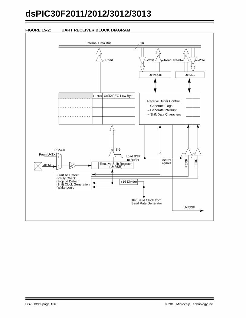
dsPIC30F2011/2012/3012/3013
FIGURE 15-2: UART RECEIVER BLOCK DIAGRAMRead
URX8 UxRXREG Low Byte
Load RSR
UxMODE
Receive Buffer Control– Generate Flags– Generate Interrupt
UxRXIF
UxRX
· Start bit Detect
Receive Shift Register
16 Divider
ControlSignals
UxSTA
– Shift Data Characters
Read ReadWrite Write
to Buffer
8-9
(UxRSR) PER
R
FER
R
· Parity Check· Stop bit Detect· Shift Clock Generation· Wake Logic
16Internal Data Bus
1
0
LPBACKFrom UxTX
16x Baud Clock fromBaud Rate Generator
DS70139G-page 106 © 2010 Microchip Technology Inc.
dsPIC30F2011/2012/3012/3013
15.2 Enabling and Setting Up UART15.2.1 ENABLING THE UARTThe UART module is enabled by setting the UARTENbit in the UxMODE register (where x = 1 or 2). Onceenabled, the UxTX and UxRX pins are configured as anoutput and an input respectively, overriding the TRISand LAT register bit settings for the corresponding I/Oport pins. The UxTX pin is at logic ‘1’ when notransmission is taking place.
15.2.2 DISABLING THE UARTThe UART module is disabled by clearing the UARTENbit in the UxMODE register. This is the default stateafter any Reset. If the UART is disabled, all I/O pinsoperate as port pins under the control of the LAT andTRIS bits of the corresponding port pins.
Disabling the UART module resets the buffers to emptystates. Any data characters in the buffers are lost andthe baud rate counter is reset.
All error and status flags associated with the UARTmodule are reset when the module is disabled. TheURXDA, OERR, FERR, PERR, UTXEN, UTXBRK andUTXBF bits are cleared, whereas RIDLE and TRMTare set. Other control bits, including ADDEN,URXISEL<1:0>, UTXISEL, as well as the UxMODEand UxBRG registers, are not affected.
Clearing the UARTEN bit while the UART is active willabort all pending transmissions and receptions andreset the module as defined above. Re-enabling theUART will restart the UART in the same configuration.
15.2.3 ALTERNATE I/OThe alternate I/O function is enabled by setting theALTIO bit (UxMODE<10>). If ALTIO = 1, the UxATXand UxARX pins (alternate transmit and alternatereceive pins, respectively) are used by the UARTmodule instead of the UxTX and UxRX pins. IfALTIO = 0, the UxTX and UxRX pins are used by theUART module.
15.2.4 SETTING UP DATA, PARITY AND STOP BIT SELECTIONS
Control bits PDSEL<1:0> in the UxMODE register areused to select the data length and parity used in thetransmission. The data length may either be 8 bits witheven, odd or no parity, or 9 bits with no parity.
The STSEL bit determines whether one or two Stop bitswill be used during data transmission.
The default (power-on) setting of the UART is 8 bits, noparity and 1 Stop bit (typically represented as 8, N, 1).
15.3 Transmitting Data
15.3.1 TRANSMITTING IN 8-BIT DATA MODE
The following steps must be performed to transmit 8-bitdata:
1. Set up the UART:First, the data length, parity and number of Stopbits must be selected. Then, the transmit andreceive interrupt enable and priority bits aresetup in the UxMODE and UxSTA registers.Also, the appropriate baud rate value must bewritten to the UxBRG register.
2. Enable the UART by setting the UARTEN bit(UxMODE<15>).
3. Set the UTXEN bit (UxSTA<10>), therebyenabling a transmission.
4. Write the byte to be transmitted to the lower byteof UxTXREG. The value will be transferred to theTransmit Shift register (UxTSR) immediatelyand the serial bit stream will start shifting outduring the next rising edge of the baud clock.Alternatively, the data byte may be written whileUTXEN = 0, following which, the user may setUTXEN. This will cause the serial bit stream tobegin immediately because the baud clock willstart from a cleared state.
5. A transmit interrupt will be generated,depending on the value of the interrupt controlbit UTXISEL (UxSTA<15>).
15.3.2 TRANSMITTING IN 9-BIT DATA MODE
The sequence of steps involved in the transmissionof 9-bit data is similar to 8-bit transmission, except thata 16-bit data word (of which the upper 7 bits are alwaysclear) must be written to the UxTXREG register.
15.3.3 TRANSMIT BUFFER (UXTXB)The transmit buffer is 9 bits wide and 4 characters deep.Including the Transmit Shift register (UxTSR), the usereffectively has a 5-deep FIFO (First-In, First- Out) buffer.The UTXBF bit (UxSTA<9>) indicates whether thetransmit buffer is full.
If a user attempts to write to a full buffer, the new datawill not be accepted into the FIFO and no data shift willoccur within the buffer. This enables recovery from abuffer overrun condition.
The FIFO is reset during any device Reset, but is notaffected when the device enters or wakes up from aPower Saving mode.
© 2010 Microchip Technology Inc. DS70139G-page 107
dsPIC30F2011/2012/3012/3013
15.3.4 TRANSMIT INTERRUPTThe transmit interrupt flag (U1TXIF or U2TXIF) islocated in the corresponding interrupt flag register.The transmitter generates an edge to set the UxTXIFbit. The condition for generating the interrupt dependson the UTXISEL control bit:
a) If UTXISEL = 0, an interrupt is generated whena word is transferred from the transmit buffer tothe Transmit Shift register (UxTSR). This meansthat the transmit buffer has at least one emptyword.
b) If UTXISEL = 1, an interrupt is generated whena word is transferred from the transmit buffer tothe Transmit Shift register (UxTSR) and thetransmit buffer is empty.
Switching between the two Interrupt modes duringoperation is possible and sometimes offers moreflexibility.
15.3.5 TRANSMIT BREAKSetting the UTXBRK bit (UxSTA<11>) will cause theUxTX line to be driven to logic ‘0’. The UTXBRK bitoverrides all transmission activity. Therefore, the usershould generally wait for the transmitter to be Idlebefore setting UTXBRK.
To send a Break character, the UTXBRK bit must be setby software and must remain set for a minimum of 13baud clock cycles. The UTXBRK bit is then cleared bysoftware to generate Stop bits. The user must wait fora duration of at least one or two baud clock cycles inorder to ensure a valid Stop bit(s) before reloading theUxTXB, or starting other transmitter activity.Transmission of a Break character does not generate atransmit interrupt.
15.4 Receiving Data
15.4.1 RECEIVING IN 8-BIT OR 9-BIT DATA MODE
The following steps must be performed while receiving8-bit or 9-bit data:
1. Set up the UART (see Section 15.3.1“Transmitting in 8-bit data mode”).
2. Enable the UART (see Section 15.3.1“Transmitting in 8-bit data mode”).
3. A receive interrupt will be generated when oneor more data words have been received, depend-ing on the receive interrupt settings specified bythe URXISEL bits (UxSTA<7:6>).
4. Read the OERR bit to determine if an overrun errorhas occurred. The OERR bit must be reset in soft-ware.
5. Read the received data from UxRXREG. The actof reading UxRXREG will move the next word tothe top of the receive FIFO, and the PERR andFERR values will be updated.
15.4.2 RECEIVE BUFFER (UXRXB)The receive buffer is 4 words deep. Including theReceive Shift register (UxRSR), the user effectivelyhas a 5-word deep FIFO buffer.
URXDA (UxSTA<0>) = 1 indicates that the receivebuffer has data available. URXDA = 0 implies that thebuffer is empty. If a user attempts to read an emptybuffer, the old values in the buffer will be read and nodata shift will occur within the FIFO.
The FIFO is reset during any device Reset. It is notaffected when the device enters or wakes up from aPower Saving mode.
15.4.3 RECEIVE INTERRUPTThe receive interrupt flag (U1RXIF or U2RXIF) can beread from the corresponding interrupt flag register. Theinterrupt flag is set by an edge generated by thereceiver. The condition for setting the receive interruptflag depends on the settings specified bythe URXISEL<1:0> (UxSTA<7:6>) control bits.
a) If URXISEL<1:0> = 00 or 01, an interrupt isgenerated every time a data word is transferredfrom the Receive Shift register (UxRSR) to thereceive buffer. There may be one or morecharacters in the receive buffer.
b) If URXISEL<1:0> = 10, an interrupt is generatedwhen a word is transferred from the Receive Shiftregister (UxRSR) to the receive buffer, which as aresult of the transfer, contains 3 characters.
c) If URXISEL<1:0> = 11, an interrupt is set whena word is transferred from the Receive Shiftregister (UxRSR) to the receive buffer, which asa result of the transfer, contains 4 characters(i.e., becomes full).
Switching between the Interrupt modes duringoperation is possible, though generally not advisableduring normal operation.
15.5 Reception Error Handling
15.5.1 RECEIVE BUFFER OVERRUN ERROR (OERR BIT)
The OERR bit (UxSTA<1>) is set if all of the followingconditions occur:
a) The receive buffer is full.b) The Receive Shift register is full, but unable to
transfer the character to the receive buffer.c) The Stop bit of the character in the UxRSR is
detected, indicating that the UxRSR needs totransfer the character to the buffer.
Once OERR is set, no further data is shifted in UxRSR(until the OERR bit is cleared in software or a Resetoccurs). The data held in UxRSR and UxRXREGremains valid.
DS70139G-page 108 © 2010 Microchip Technology Inc.
dsPIC30F2011/2012/3012/3013
15.5.2 FRAMING ERROR (FERR)The FERR bit (UxSTA<2>) is set if a ‘0’ is detectedinstead of a Stop bit. If two Stop bits are selected, bothStop bits must be ‘1’, otherwise FERR will be set. Theread-only FERR bit is buffered along with the receiveddata. It is cleared on any Reset.15.5.3 PARITY ERROR (PERR)The PERR bit (UxSTA<3>) is set if the parity of thereceived word is incorrect. This error bit is applicableonly if a Parity mode (odd or even) is selected. Theread-only PERR bit is buffered along with the receiveddata bytes. It is cleared on any Reset.
15.5.4 IDLE STATUSWhen the receiver is active (i.e., between the initialdetection of the Start bit and the completion of the Stopbit), the RIDLE bit (UxSTA<4>) is ‘0’. Between the com-pletion of the Stop bit and detection of the next Start bit,the RIDLE bit is ‘1’, indicating that the UART is Idle.
15.5.5 RECEIVE BREAKThe receiver will count and expect a certain number ofbit times based on the values programmed in the PDSEL(UxMODE<2:1>) and STSEL (UxMODE<0>) bits.
If the break is longer than 13 bit times, the reception isconsidered complete after the number of bit timesspecified by PDSEL and STSEL. The URXDA bit is set,FERR is set, zeros are loaded into the receive FIFO,interrupts are generated if appropriate and the RIDLEbit is set.
When the module receives a long break signal and thereceiver has detected the Start bit, the data bits and theinvalid Stop bit (which sets the FERR), the receivermust wait for a valid Stop bit before looking for the nextStart bit. It cannot assume that the break condition onthe line is the next Start bit.
Break is regarded as a character containing all ‘0’s withthe FERR bit set. The Break character is loaded intothe buffer. No further reception can occur until a Stop bitis received. Note that RIDLE goes high when the Stopbit has not yet been received.
15.6 Address Detect ModeSetting the ADDEN bit (UxSTA<5>) enables thisspecial mode in which a 9th bit (URX8) value of ‘1’identifies the received word as an address, rather thandata. This mode is only applicable for 9-bit datacommunication. The URXISEL control bit does nothave any impact on interrupt generation in this modesince an interrupt (if enabled) will be generated everytime the received word has the 9th bit set.
15.7 Loopback ModeSetting the LPBACK bit enables this special mode inwhich the UxTX pin is internally connected to the UxRXpin. When configured for the Loopback mode, theUxRX pin is disconnected from the internal UARTreceive logic. However, the UxTX pin still functions asin a normal operation.
To select this mode:
a) Configure UART for desired mode of operation.b) Set LPBACK = 1 to enable Loopback mode.c) Enable transmission as defined in Section 15.3
“Transmitting Data”.
15.8 Baud Rate GeneratorThe UART has a 16-bit Baud Rate Generator to allowmaximum flexibility in baud rate generation. The BaudRate Generator register (UxBRG) is readable andwritable. The baud rate is computed as follows:
BRG = 16-bit value held in UxBRG register (0 through 65535)
FCY = Instruction Clock Rate (1/TCY)
The baud rate is given by Equation 15-1.
EQUATION 15-1: BAUD RATE
Therefore, the maximum baud rate possible is:
FCY /16 (if BRG = 0),
and the minimum baud rate possible is:
FCY / (16* 65536).
With a full 16-bit Baud Rate Generator at 30 MIPSoperation, the minimum baud rate achievable is28.5 bps.
15.9 Auto-Baud SupportTo allow the system to determine baud rates ofreceived characters, the input can be optionally linkedto a selected capture input (IC1 for UART1 and IC2 forUART2). To enable this mode, you must program theinput capture module to detect the falling and risingedges of the Start bit.
Baud Rate = FCY / (16*(BRG+1))
© 2010 Microchip Technology Inc. DS70139G-page 109
dsPIC30F2011/2012/3012/3013
15.10 UART Operation During CPUSleep and Idle Modes
15.10.1 UART OPERATION DURING CPU SLEEP MODE
When the device enters Sleep mode, all clock sourcesto the module are shut down and stay at logic ‘0’. Ifentry into Sleep mode occurs while a transmission is inprogress, then the transmission is aborted. The UxTXpin is driven to logic ‘1’. Similarly, if entry into Sleepmode occurs while a reception is in progress, then thereception is aborted. The UxSTA, UxMODE, transmitand receive registers and buffers, and the UxBRGregister are not affected by Sleep mode.
If the WAKE bit (UxMODE<7>) is set before the deviceenters Sleep mode, then a falling edge on the UxRX pinwill generate a receive interrupt. The Receive InterruptSelect mode bit (URXISEL) has no effect for thisfunction. If the receive interrupt is enabled, then this willwake-up the device from Sleep. The UARTEN bit mustbe set in order to generate a wake-up interrupt.
15.10.2 UART OPERATION DURING CPU IDLE MODE
For the UART, the USIDL bit selects if the module willstop operation when the device enters Idle mode orwhether the module will continue on Idle. If USIDL = 0,the module will continue to operate during Idle mode. IfUSIDL = 1, the module will stop on Idle.
DS70139G-page 110 © 2010 Microchip Technology Inc.
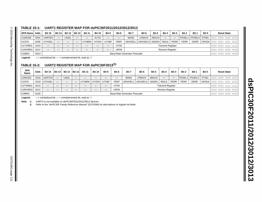
© 2010 M
icrochip Technology Inc.D
S70139G
-page 111
dsPIC30F2011/2012/3012/3013
TA
TA
SF 2 Bit 1 Bit 0 Reset State
U1 EL1 PDSEL0 STSEL 0000 0000 0000 0000
U1 R OERR URXDA 0000 0001 0001 0000
U1 0000 000u uuuu uuuu
U1 0000 0000 0000 0000
U1 0000 0000 0000 0000
Le
2 Bit 1 Bit 0 Reset State
U2 L1 PDSEL0 STSEL 0000 0000 0000 0000
U2 R OERR URXDA 0000 0001 0001 0000
U2 0000 000u uuuu uuuu
U2 0000 0000 0000 0000
U2 0000 0000 0000 0000
LeNo
BLE 15-1: UART1 REGISTER MAP FOR dsPIC30F2011/2012/3012/3013
BLE 15-2: UART2 REGISTER MAP FOR dsPIC30F3013(1)
R Name Addr. Bit 15 Bit 14 Bit 13 Bit 12 Bit 11 Bit 10 Bit 9 Bit 8 Bit 7 Bit 6 Bit 5 Bit 4 Bit 3 Bit
MODE 020C UARTEN — USIDL — — ALTIO — — WAKE LPBACK ABAUD — — PDS
STA 020E UTXISEL — — — UTXBRK UTXEN UTXBF TRMT URXISEL1 URXISEL0 ADDEN RIDLE PERR FER
TXREG 0210 — — — — — — — UTX8 Transmit Register
RXREG 0212 — — — — — — — URX8 Receive Register
BRG 0214 Baud Rate Generator Prescaler
gend: u = uninitialized bit; — = unimplemented bit, read as ‘0’
SFR Name Addr. Bit 15 Bit 14 Bit 13 Bit 12 Bit 11 Bit 10 Bit 9 Bit 8 Bit 7 Bit 6 Bit 5 Bit 4 Bit 3 Bit
MODE 0216 UARTEN — USIDL — — — — — WAKE LPBACK ABAUD — — PDSE
STA 0218 UTXISEL — — — UTXBRK UTXEN UTXBF TRMT URXISEL1 URXISEL0 ADDEN RIDLE PERR FER
TXREG 021A — — — — — — — UTX8 Transmit Register
RXREG 021C — — — — — — — URX8 Receive Register
BRG 021E Baud Rate Generator Prescaler
gend: u = uninitialized bit; — = unimplemented bit, read as ‘0’
te 1: UART2 is not available on dsPIC30F2011/2012/3012 devices.2: Refer to the “dsPIC30F Family Reference Manual” (DS70046) for descriptions of register bit fields.

dsPIC30F2011/2012/3012/3013
NOTES:DS70139G-page 112 © 2010 Microchip Technology Inc.
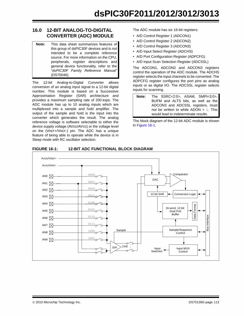
dsPIC30F2011/2012/3012/3013
16.0 12-BIT ANALOG-TO-DIGITAL CONVERTER (ADC) MODULE
The 12-bit Analog-to-Digital Converter allowsconversion of an analog input signal to a 12-bit digitalnumber. This module is based on a SuccessiveApproximation Register (SAR) architecture andprovides a maximum sampling rate of 200 ksps. TheADC module has up to 10 analog inputs which aremultiplexed into a sample and hold amplifier. Theoutput of the sample and hold is the input into theconverter which generates the result. The analogreference voltage is software selectable to either thedevice supply voltage (AVDD/AVSS) or the voltage levelon the (VREF+/VREF-) pin. The ADC has a uniquefeature of being able to operate while the device is inSleep mode with RC oscillator selection.
The ADC module has six 16-bit registers:
• A/D Control Register 1 (ADCON1)• A/D Control Register 2 (ADCON2)• A/D Control Register 3 (ADCON3)• A/D Input Select Register (ADCHS)• A/D Port Configuration Register (ADPCFG)• A/D Input Scan Selection Register (ADCSSL)
The ADCON1, ADCON2 and ADCON3 registerscontrol the operation of the ADC module. The ADCHSregister selects the input channels to be converted. TheADPCFG register configures the port pins as analoginputs or as digital I/O. The ADCSSL register selectsinputs for scanning.
The block diagram of the 12-bit ADC module is shownin Figure 16-1.
FIGURE 16-1: 12-BIT ADC FUNCTIONAL BLOCK DIAGRAM
Note: This data sheet summarizes features ofthis group of dsPIC30F devices and is notintended to be a complete referencesource. For more information on the CPU,peripherals, register descriptions andgeneral device functionality, refer to the“dsPIC30F Family Reference Manual”(DS70046).
Note: The SSRC<2:0>, ASAM, SMPI<3:0>,BUFM and ALTS bits, as well as theADCON3 and ADCSSL registers, mustnot be written to while ADON = 1. Thiswould lead to indeterminate results.
Comparator
12-bit SAR Conversion Logic
AVDD/VREF+
DAC
Dat
a Fo
rmat
16-word, 12-bitDual Port
Buffer
Bus
Inte
rface
0000
0101
0111
1001
0001
0010
0011
0100
0110
1000AN8
AN9
AN4
AN5
AN6
AN7
AN0
AN1
AN2
AN3
CH0
AVSS/VREF-
Sample/SequenceControl
Sample
Input MUXControl
InputSwitches
S/H
© 2010 Microchip Technology Inc. DS70139G-page 113
dsPIC30F2011/2012/3012/3013
16.1 A/D Result BufferThe module contains a 16-word dual port read-onlybuffer, called ADCBUF0...ADCBUFF, to buffer the A/Dresults. The RAM is 12 bits wide but the data obtainedis represented in one of four different 16-bit dataformats. The contents of the sixteen A/D ConversionResult Buffer registers, ADCBUF0 through ADCBUFF,cannot be written by user software.16.2 Conversion OperationAfter the ADC module has been configured, the sampleacquisition is started by setting the SAMP bit. Varioussources, such as a programmable bit, timer time-outsand external events, will terminate acquisition and starta conversion. When the A/D conversion is complete,the result is loaded into ADCBUF0...ADCBUFF, andthe DONE bit and the A/D interrupt flag, ADIF, are setafter the number of samples specified by the SMPI bit.The ADC module can be configured for different inter-rupt rates as described in Section 16.3 “Selecting theConversion Sequence”.
The following steps should be followed for doing anA/D conversion:
1. Configure the ADC module:• Configure analog pins, voltage reference and
digital I/O• Select A/D input channels• Select A/D conversion clock• Select A/D conversion trigger• Turn on ADC module
2. Configure A/D interrupt (if required):• Clear ADIF bit • Select A/D interrupt priority
3. Start sampling4. Wait the required acquisition time5. Trigger acquisition end, start conversion6. Wait for A/D conversion to complete, by either:
• Waiting for the A/D interrupt, or• Waiting for the DONE bit to get set
7. Read A/D result buffer; clear ADIF if required
16.3 Selecting the Conversion Sequence
Several groups of control bits select the sequence inwhich the A/D connects inputs to the sample/holdchannel, converts a channel, writes the buffer memoryand generates interrupts.
The sequence is controlled by the sampling clocks.
The SMPI bits select the number ofacquisition/conversion sequences that would be per-formed before an interrupt occurs. This can vary from 1sample per interrupt to 16 samples per interrupt.
The BUFM bit will split the 16-word results buffer intotwo 8-word groups. Writing to the 8-word buffers will bealternated on each interrupt event.
Use of the BUFM bit will depend on how much time isavailable for the moving of the buffers after theinterrupt.
If the processor can quickly unload a full buffer withinthe time it takes to acquire and convert one channel,the BUFM bit can be ‘0’ and up to 16 conversions(corresponding to the 16 input channels) may be doneper interrupt. The processor will have one acquisitionand conversion time to move the sixteen conversions.
If the processor cannot unload the buffer within theacquisition and conversion time, the BUFM bit should be‘1’. For example, if SMPI<3:0> (ADCON2<5:2>) = 0111,then eight conversions will be loaded into 1/2 of thebuffer, following which an interrupt occurs. The nexteight conversions will be loaded into the other 1/2 of thebuffer. The processor will have the entire time betweeninterrupts to move the eight conversions.
The ALTS bit can be used to alternate the inputsselected during the sampling sequence. The inputmultiplexer has two sets of sample inputs: MUX A andMUX B. If the ALTS bit is ‘0’, only the MUX A inputs areselected for sampling. If the ALTS bit is ‘1’ andSMPI<3:0> = 0000 on the first sample/convertsequence, the MUX A inputs are selected and on thenext acquire/convert sequence, the MUX B inputs areselected.
The CSCNA bit (ADCON2<10>) will allow themultiplexer input to be alternately scanned across aselected number of analog inputs for the MUX A group.The inputs are selected by the ADCSSL register. If aparticular bit in the ADCSSL register is ‘1’, thecorresponding input is selected. The inputs are alwaysscanned from lower to higher numbered inputs, startingafter each interrupt. If the number of inputs selected isgreater than the number of samples taken per interrupt,the higher numbered inputs are unused.
DS70139G-page 114 © 2010 Microchip Technology Inc.
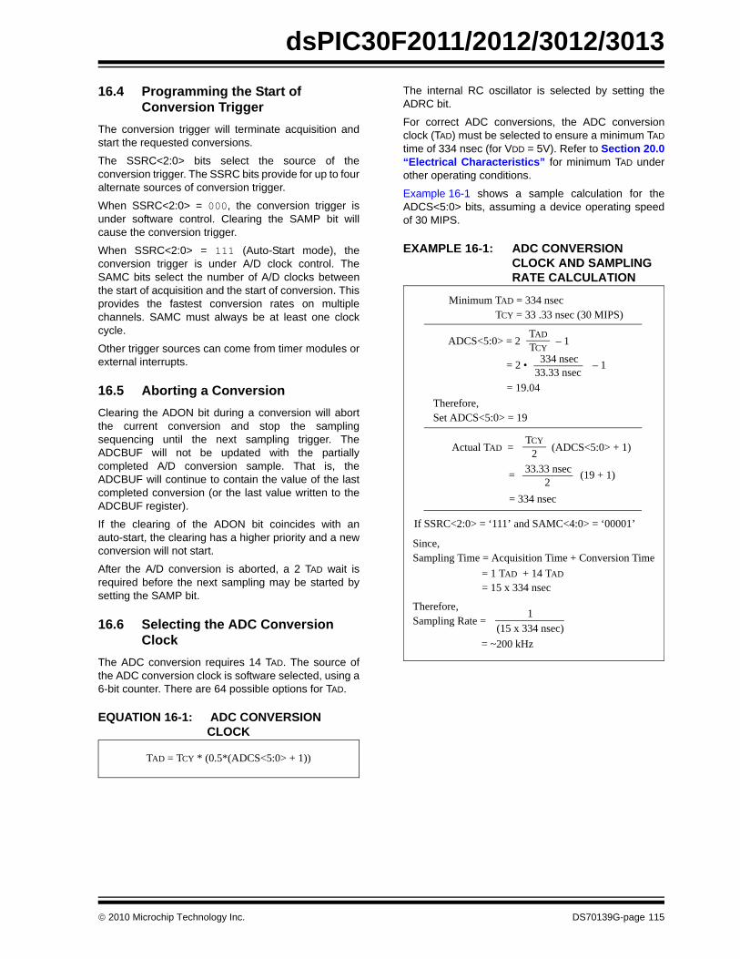
dsPIC30F2011/2012/3012/3013
16.4 Programming the Start ofConversion TriggerThe conversion trigger will terminate acquisition andstart the requested conversions.
The SSRC<2:0> bits select the source of theconversion trigger. The SSRC bits provide for up to fouralternate sources of conversion trigger.
When SSRC<2:0> = 000, the conversion trigger isunder software control. Clearing the SAMP bit willcause the conversion trigger.
When SSRC<2:0> = 111 (Auto-Start mode), theconversion trigger is under A/D clock control. TheSAMC bits select the number of A/D clocks betweenthe start of acquisition and the start of conversion. Thisprovides the fastest conversion rates on multiplechannels. SAMC must always be at least one clockcycle.
Other trigger sources can come from timer modules orexternal interrupts.
16.5 Aborting a ConversionClearing the ADON bit during a conversion will abortthe current conversion and stop the samplingsequencing until the next sampling trigger. TheADCBUF will not be updated with the partiallycompleted A/D conversion sample. That is, theADCBUF will continue to contain the value of the lastcompleted conversion (or the last value written to theADCBUF register).
If the clearing of the ADON bit coincides with anauto-start, the clearing has a higher priority and a newconversion will not start.
After the A/D conversion is aborted, a 2 TAD wait isrequired before the next sampling may be started bysetting the SAMP bit.
16.6 Selecting the ADC Conversion Clock
The ADC conversion requires 14 TAD. The source ofthe ADC conversion clock is software selected, using a6-bit counter. There are 64 possible options for TAD.
EQUATION 16-1: ADC CONVERSION CLOCK
The internal RC oscillator is selected by setting theADRC bit.
For correct ADC conversions, the ADC conversionclock (TAD) must be selected to ensure a minimum TADtime of 334 nsec (for VDD = 5V). Refer to Section 20.0“Electrical Characteristics” for minimum TAD underother operating conditions.
Example 16-1 shows a sample calculation for theADCS<5:0> bits, assuming a device operating speedof 30 MIPS.
EXAMPLE 16-1: ADC CONVERSION CLOCK AND SAMPLING RATE CALCULATION
TAD = TCY * (0.5*(ADCS<5:0> + 1))
Minimum TAD = 334 nsec
ADCS<5:0> = 2 – 1TADTCY
TCY = 33 .33 nsec (30 MIPS)
= 2 • – 1334 nsec33.33 nsec
= 19.04 Therefore,Set ADCS<5:0> = 19
Actual TAD = (ADCS<5:0> + 1)TCY
2
= (19 + 1)33.33 nsec2
= 334 nsec
If SSRC<2:0> = ‘111’ and SAMC<4:0> = ‘00001’
Since,Sampling Time = Acquisition Time + Conversion Time
= 1 TAD + 14 TAD = 15 x 334 nsec
Therefore,Sampling Rate =
= ~200 kHz
1(15 x 334 nsec)
© 2010 Microchip Technology Inc. DS70139G-page 115
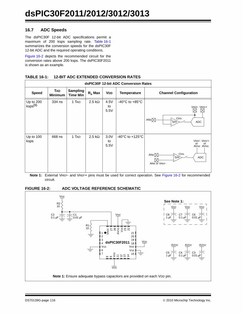
dsPIC30F2011/2012/3012/3013
16.7 ADC SpeedsThe dsPIC30F 12-bit ADC specifications permit amaximum of 200 ksps sampling rate. Table 16-1summarizes the conversion speeds for the dsPIC30F12-bit ADC and the required operating conditions.Figure 16-2 depicts the recommended circuit for theconversion rates above 200 ksps. The dsPIC30F2011is shown as an example.
FIGURE 16-2: ADC VOLTAGE REFERENCE SCHEMATIC
TABLE 16-1: 12-BIT ADC EXTENDED CONVERSION RATESdsPIC30F 12-bit ADC Conversion Rates
Speed TAD Minimum
Sampling Time Min Rs Max VDD Temperature Channel Configuration
Up to 200 ksps(1)
334 ns 1 TAD 2.5 kΩ 4.5V to
5.5V
-40°C to +85°C
Up to 100 ksps
668 ns 1 TAD 2.5 kΩ 3.0V to
5.5V
-40°C to +125°C
Note 1: External VREF- and VREF+ pins must be used for correct operation. See Figure 16-2 for recommendedcircuit.
VREF- VREF+
ADCANx
S/HCHX
VREF- VREF+
ADCANx
S/HCHX
ANx or VREF-
orAVSS
orAVDD
VDD
VDD
VDD
C81 μF
VDD
C70.1 μF
VDD
C60.01 μF
AVDD
C51 μF
AVDD
C40.1 μF
AVDD
C30.01 μF
See Note 1:
Note 1: Ensure adequate bypass capacitors are provided on each VDD pin.
VRE
F- 27 26A
VD
D
VS
S23 22
8 9 VD
D11 12 13 14
1234VSS67
21201918
VDD
VSS15
dsPIC30F2011
VDD
R110
VDD
R210
C20.1 μF
C10.01 μF
DS70139G-page 116 © 2010 Microchip Technology Inc.
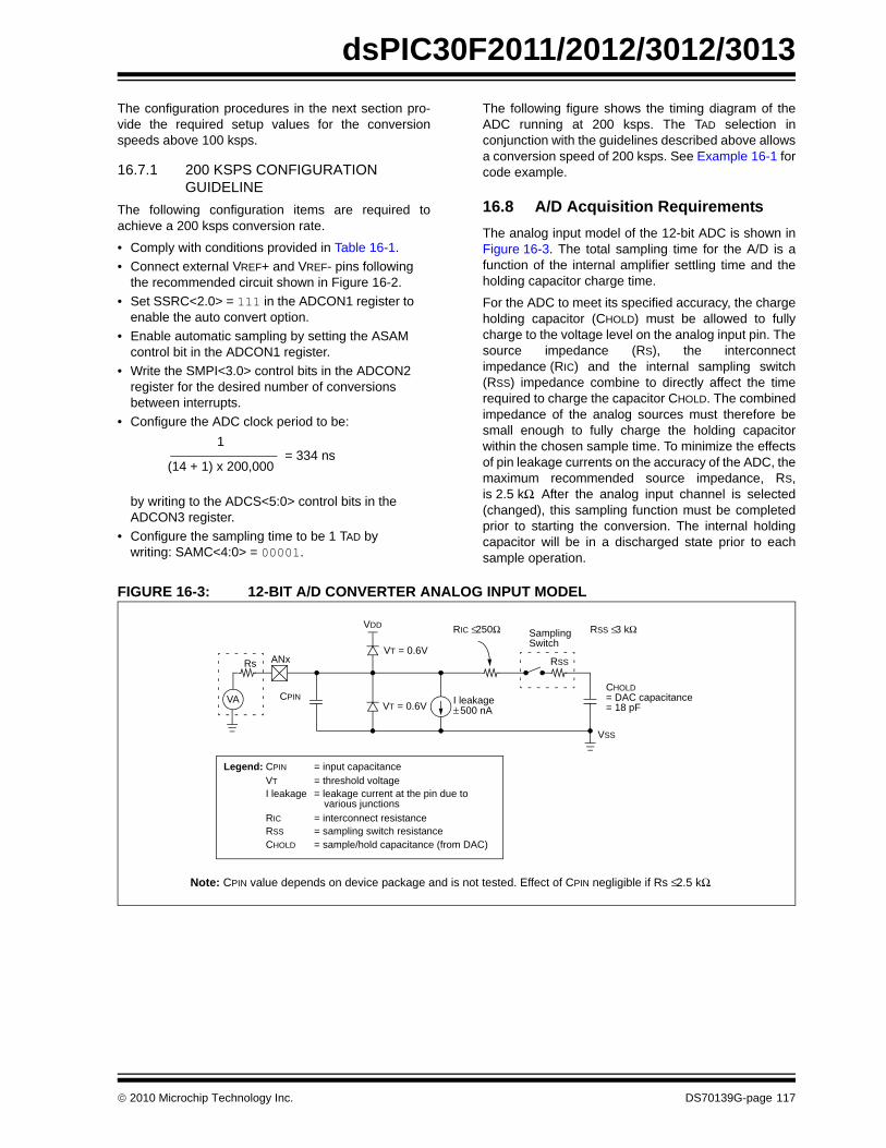
dsPIC30F2011/2012/3012/3013
The configuration procedures in the next section pro-vide the required setup values for the conversionspeeds above 100 ksps.16.7.1 200 KSPS CONFIGURATION GUIDELINE
The following configuration items are required toachieve a 200 ksps conversion rate.
• Comply with conditions provided in Table 16-1.• Connect external VREF+ and VREF- pins following
the recommended circuit shown in Figure 16-2.• Set SSRC<2.0> = 111 in the ADCON1 register to
enable the auto convert option.• Enable automatic sampling by setting the ASAM
control bit in the ADCON1 register.• Write the SMPI<3.0> control bits in the ADCON2
register for the desired number of conversions between interrupts.
• Configure the ADC clock period to be:
by writing to the ADCS<5:0> control bits in the ADCON3 register.
• Configure the sampling time to be 1 TAD by writing: SAMC<4:0> = 00001.
The following figure shows the timing diagram of theADC running at 200 ksps. The TAD selection inconjunction with the guidelines described above allowsa conversion speed of 200 ksps. See Example 16-1 forcode example.
16.8 A/D Acquisition RequirementsThe analog input model of the 12-bit ADC is shown inFigure 16-3. The total sampling time for the A/D is afunction of the internal amplifier settling time and theholding capacitor charge time.
For the ADC to meet its specified accuracy, the chargeholding capacitor (CHOLD) must be allowed to fullycharge to the voltage level on the analog input pin. Thesource impedance (RS), the interconnectimpedance (RIC) and the internal sampling switch(RSS) impedance combine to directly affect the timerequired to charge the capacitor CHOLD. The combinedimpedance of the analog sources must therefore besmall enough to fully charge the holding capacitorwithin the chosen sample time. To minimize the effectsof pin leakage currents on the accuracy of the ADC, themaximum recommended source impedance, RS,is 2.5 kΩ. After the analog input channel is selected(changed), this sampling function must be completedprior to starting the conversion. The internal holdingcapacitor will be in a discharged state prior to eachsample operation.
FIGURE 16-3: 12-BIT A/D CONVERTER ANALOG INPUT MODEL
1
(14 + 1) x 200,000= 334 ns
CPINVA
Rs ANxVT = 0.6V
VT = 0.6V I leakage
RIC ≤ 250Ω SamplingSwitch
RSS
CHOLD= DAC capacitance
VSS
VDD
= 18 pF± 500 nA
Legend: CPIN
VTI leakage
RICRSS
CHOLD
= input capacitance= threshold voltage= leakage current at the pin due to
= interconnect resistance= sampling switch resistance= sample/hold capacitance (from DAC)
various junctions
Note: CPIN value depends on device package and is not tested. Effect of CPIN negligible if Rs ≤ 2.5 kΩ.
RSS ≤ 3 kΩ
© 2010 Microchip Technology Inc. DS70139G-page 117
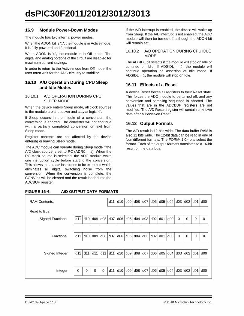
dsPIC30F2011/2012/3012/3013
16.9 Module Power-Down ModesThe module has two internal power modes.When the ADON bit is ‘1’, the module is in Active mode;it is fully powered and functional.
When ADON is ‘0’, the module is in Off mode. Thedigital and analog portions of the circuit are disabled formaximum current savings.
In order to return to the Active mode from Off mode, theuser must wait for the ADC circuitry to stabilize.
16.10 A/D Operation During CPU Sleep and Idle Modes
16.10.1 A/D OPERATION DURING CPU SLEEP MODE
When the device enters Sleep mode, all clock sourcesto the module are shut down and stay at logic ‘0’.
If Sleep occurs in the middle of a conversion, theconversion is aborted. The converter will not continuewith a partially completed conversion on exit fromSleep mode.
Register contents are not affected by the deviceentering or leaving Sleep mode.
The ADC module can operate during Sleep mode if theA/D clock source is set to RC (ADRC = 1). When theRC clock source is selected, the ADC module waitsone instruction cycle before starting the conversion.This allows the SLEEP instruction to be executed whicheliminates all digital switching noise from theconversion. When the conversion is complete, theCONV bit will be cleared and the result loaded into theADCBUF register.
If the A/D interrupt is enabled, the device will wake-upfrom Sleep. If the A/D interrupt is not enabled, the ADCmodule will then be turned off, although the ADON bitwill remain set.
16.10.2 A/D OPERATION DURING CPU IDLE MODE
The ADSIDL bit selects if the module will stop on Idle orcontinue on Idle. If ADSIDL = 0, the module willcontinue operation on assertion of Idle mode. IfADSIDL = 1, the module will stop on Idle.
16.11 Effects of a ResetA device Reset forces all registers to their Reset state.This forces the ADC module to be turned off, and anyconversion and sampling sequence is aborted. Thevalues that are in the ADCBUF registers are notmodified. The A/D Result register will contain unknowndata after a Power-on Reset.
16.12 Output FormatsThe A/D result is 12 bits wide. The data buffer RAM isalso 12 bits wide. The 12-bit data can be read in one offour different formats. The FORM<1:0> bits select theformat. Each of the output formats translates to a 16-bitresult on the data bus.
FIGURE 16-4: A/D OUTPUT DATA FORMATS
RAM Contents: d11 d10 d09 d08 d07 d06 d05 d04 d03 d02 d01 d00
Read to Bus:
Signed Fractional d11 d10 d09 d08 d07 d06 d05 d04 d03 d02 d01 d00 0 0 0 0
Fractional d11 d10 d09 d08 d07 d06 d05 d04 d03 d02 d01 d00 0 0 0 0
Signed Integer d11 d11 d11 d11 d11 d10 d09 d08 d07 d06 d05 d04 d03 d02 d01 d00
Integer 0 0 0 0 d11 d10 d09 d08 d07 d06 d05 d04 d03 d02 d01 d00
DS70139G-page 118 © 2010 Microchip Technology Inc.
dsPIC30F2011/2012/3012/3013
16.13 Configuring Analog Port PinsThe use of the ADPCFG and TRIS registers control theoperation of the A/D port pins. The port pins that aredesired as analog inputs must have theircorresponding TRIS bit set (input). If the TRIS bit iscleared (output), the digital output level (VOH or VOL)will be converted.The A/D operation is independent of the state of theCH0SA<3:0>/CH0SB<3:0> bits and the TRIS bits.
When reading the PORT register, all pins configured asanalog input channels will read as cleared.
Pins configured as digital inputs will not convert ananalog input. Analog levels on any pin that is defined asa digital input (including the ANx pins) may cause theinput buffer to consume current that exceeds thedevice specifications.
16.14 Connection ConsiderationsThe analog inputs have diodes to VDD and VSS as ESDprotection. This requires that the analog input bebetween VDD and VSS. If the input voltage exceeds thisrange by greater than 0.3V (either direction), one of thediodes becomes forward biased and it may damage thedevice if the input current specification is exceeded.
An external RC filter is sometimes added foranti-aliasing of the input signal. The R componentshould be selected to ensure that the sampling timerequirements are satisfied. Any external componentsconnected (via high-impedance) to an analog input pin(capacitor, zener diode, etc.) should have very littleleakage current at the pin.
© 2010 Microchip Technology Inc. DS70139G-page 119
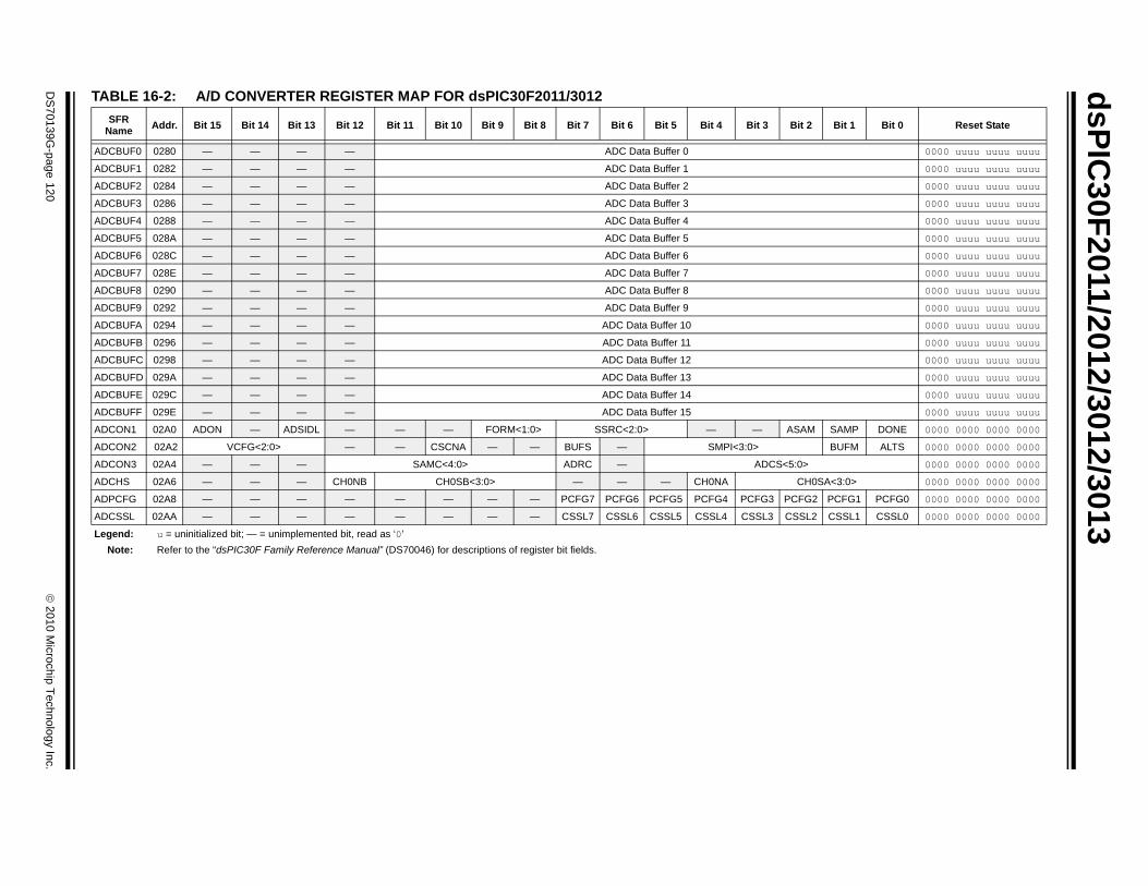
dsPIC30F2011/2012/3012/3013
DS
70139G-page 120
© 2010 M
icrochip Technology Inc.
Bit 2 Bit 1 Bit 0 Reset State
0000 uuuu uuuu uuuu
0000 uuuu uuuu uuuu
0000 uuuu uuuu uuuu
0000 uuuu uuuu uuuu
0000 uuuu uuuu uuuu
0000 uuuu uuuu uuuu
0000 uuuu uuuu uuuu
0000 uuuu uuuu uuuu
0000 uuuu uuuu uuuu
0000 uuuu uuuu uuuu
0000 uuuu uuuu uuuu
0000 uuuu uuuu uuuu
0000 uuuu uuuu uuuu
0000 uuuu uuuu uuuu
0000 uuuu uuuu uuuu
0000 uuuu uuuu uuuu
ASAM SAMP DONE 0000 0000 0000 0000
BUFM ALTS 0000 0000 0000 0000
5:0> 0000 0000 0000 0000
CH0SA<3:0> 0000 0000 0000 0000
PCFG2 PCFG1 PCFG0 0000 0000 0000 0000
CSSL2 CSSL1 CSSL0 0000 0000 0000 0000
TABLE 16-2: A/D CONVERTER REGISTER MAP FOR dsPIC30F2011/3012SFR
Name Addr. Bit 15 Bit 14 Bit 13 Bit 12 Bit 11 Bit 10 Bit 9 Bit 8 Bit 7 Bit 6 Bit 5 Bit 4 Bit 3
ADCBUF0 0280 — — — — ADC Data Buffer 0
ADCBUF1 0282 — — — — ADC Data Buffer 1
ADCBUF2 0284 — — — — ADC Data Buffer 2
ADCBUF3 0286 — — — — ADC Data Buffer 3
ADCBUF4 0288 — — — — ADC Data Buffer 4
ADCBUF5 028A — — — — ADC Data Buffer 5
ADCBUF6 028C — — — — ADC Data Buffer 6
ADCBUF7 028E — — — — ADC Data Buffer 7
ADCBUF8 0290 — — — — ADC Data Buffer 8
ADCBUF9 0292 — — — — ADC Data Buffer 9
ADCBUFA 0294 — — — — ADC Data Buffer 10
ADCBUFB 0296 — — — — ADC Data Buffer 11
ADCBUFC 0298 — — — — ADC Data Buffer 12
ADCBUFD 029A — — — — ADC Data Buffer 13
ADCBUFE 029C — — — — ADC Data Buffer 14
ADCBUFF 029E — — — — ADC Data Buffer 15
ADCON1 02A0 ADON — ADSIDL — — — FORM<1:0> SSRC<2:0> — —
ADCON2 02A2 VCFG<2:0> — — CSCNA — — BUFS — SMPI<3:0>
ADCON3 02A4 — — — SAMC<4:0> ADRC — ADCS<
ADCHS 02A6 — — — CH0NB CH0SB<3:0> — — — CH0NA
ADPCFG 02A8 — — — — — — — — PCFG7 PCFG6 PCFG5 PCFG4 PCFG3
ADCSSL 02AA — — — — — — — — CSSL7 CSSL6 CSSL5 CSSL4 CSSL3
Legend: u = uninitialized bit; — = unimplemented bit, read as ‘0’Note: Refer to the “dsPIC30F Family Reference Manual” (DS70046) for descriptions of register bit fields.
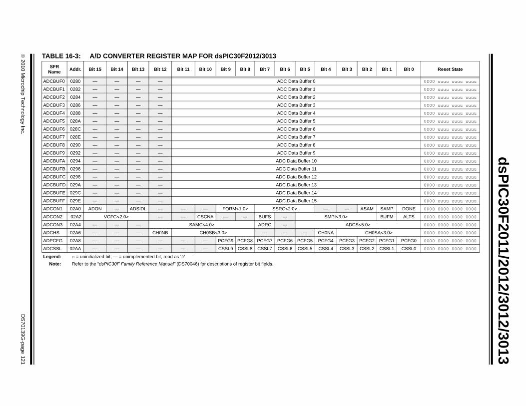
© 2010 M
icrochip Technology Inc.D
S70139G
-page 121
dsPIC30F2011/2012/3012/3013
TA
Bit 1 Bit 0 Reset State
AD 0000 uuuu uuuu uuuu
AD 0000 uuuu uuuu uuuu
AD 0000 uuuu uuuu uuuu
AD 0000 uuuu uuuu uuuu
AD 0000 uuuu uuuu uuuu
AD 0000 uuuu uuuu uuuu
AD 0000 uuuu uuuu uuuu
AD 0000 uuuu uuuu uuuu
AD 0000 uuuu uuuu uuuu
AD 0000 uuuu uuuu uuuu
AD 0000 uuuu uuuu uuuu
AD 0000 uuuu uuuu uuuu
AD 0000 uuuu uuuu uuuu
AD 0000 uuuu uuuu uuuu
AD 0000 uuuu uuuu uuuu
AD 0000 uuuu uuuu uuuu
AD SAMP DONE 0000 0000 0000 0000
AD BUFM ALTS 0000 0000 0000 0000
AD 0000 0000 0000 0000
AD 0SA<3:0> 0000 0000 0000 0000
AD 2 PCFG1 PCFG0 0000 0000 0000 0000
AD 2 CSSL1 CSSL0 0000 0000 0000 0000
Le
BLE 16-3: A/D CONVERTER REGISTER MAP FOR dsPIC30F2012/3013SFR
Name Addr. Bit 15 Bit 14 Bit 13 Bit 12 Bit 11 Bit 10 Bit 9 Bit 8 Bit 7 Bit 6 Bit 5 Bit 4 Bit 3 Bit 2
CBUF0 0280 — — — — ADC Data Buffer 0
CBUF1 0282 — — — — ADC Data Buffer 1
CBUF2 0284 — — — — ADC Data Buffer 2
CBUF3 0286 — — — — ADC Data Buffer 3
CBUF4 0288 — — — — ADC Data Buffer 4
CBUF5 028A — — — — ADC Data Buffer 5
CBUF6 028C — — — — ADC Data Buffer 6
CBUF7 028E — — — — ADC Data Buffer 7
CBUF8 0290 — — — — ADC Data Buffer 8
CBUF9 0292 — — — — ADC Data Buffer 9
CBUFA 0294 — — — — ADC Data Buffer 10
CBUFB 0296 — — — — ADC Data Buffer 11
CBUFC 0298 — — — — ADC Data Buffer 12
CBUFD 029A — — — — ADC Data Buffer 13
CBUFE 029C — — — — ADC Data Buffer 14
CBUFF 029E — — — — ADC Data Buffer 15
CON1 02A0 ADON — ADSIDL — — — FORM<1:0> SSRC<2:0> — — ASAM
CON2 02A2 VCFG<2:0> — — CSCNA — — BUFS — SMPI<3:0>
CON3 02A4 — — — SAMC<4:0> ADRC — ADCS<5:0>
CHS 02A6 — — — CH0NB CH0SB<3:0> — — — CH0NA CH
PCFG 02A8 — — — — — — PCFG9 PCFG8 PCFG7 PCFG6 PCFG5 PCFG4 PCFG3 PCFG
CSSL 02AA — — — — — — CSSL9 CSSL8 CSSL7 CSSL6 CSSL5 CSSL4 CSSL3 CSSL
gend: u = uninitialized bit; — = unimplemented bit, read as ‘0’Note: Refer to the “dsPIC30F Family Reference Manual” (DS70046) for descriptions of register bit fields.

dsPIC30F2011/2012/3012/3013
NOTES:DS70139G-page 122 © 2010 Microchip Technology Inc.
dsPIC30F2011/2012/3012/3013
17.0 SYSTEM INTEGRATION
There are several features intended to maximizesystem reliability, minimize cost through elimination ofexternal components, provide Power Saving Operatingmodes and offer code protection:
• Oscillator Selection• Reset
- Power-on Reset (POR)- Power-up Timer (PWRT)- Oscillator Start-up Timer (OST)- Programmable Brown-out Reset (BOR)
• Watchdog Timer (WDT)• Low-Voltage Detect• Power-Saving Modes (Sleep and Idle)• Code Protection• Unit ID Locations• In-Circuit Serial Programming (ICSP)
dsPIC30F devices have a Watchdog Timer which ispermanently enabled via the Configuration bits or canbe software controlled. It runs off its own RC oscillatorfor added reliability. There are two timers that offernecessary delays on power-up. One is the OscillatorStart-up Timer (OST), intended to keep the chip inReset until the crystal oscillator is stable. The other isthe Power-up Timer (PWRT) which provides a delay onpower-up only, designed to keep the part in Reset whilethe power supply stabilizes. With these two timerson-chip, most applications need no external Resetcircuitry.
Sleep mode is designed to offer a very low currentPower-Down mode. The user can wake-up from Sleepthrough external Reset, Watchdog Timer Wake-up, orthrough an interrupt. Several oscillator options are alsomade available to allow the part to fit a wide variety ofapplications. In the Idle mode, the clock sources arestill active but the CPU is shut-off. The RC oscillatoroption saves system cost while the LP crystal optionsaves power.
17.1 Oscillator System OverviewThe dsPIC30F oscillator system has the followingmodules and features:
• Various external and internal oscillator options as clock sources
• An on-chip PLL to boost internal operating frequency
• A clock switching mechanism between various clock sources
• Programmable clock postscaler for system power savings
• A Fail-Safe Clock Monitor (FSCM) that detects clock failure and takes fail-safe measures
• Clock Control register (OSCCON)• Configuration bits for main oscillator selection
Configuration bits determine the clock source uponPower-on Reset (POR) and Brown-out Reset (BOR).Thereafter, the clock source can be changed betweenpermissible clock sources. The OSCCON registercontrols the clock switching and reflects system clockrelated status bits.
Table 17-1 provides a summary of the dsPIC30FOscillator Operating modes. A simplified diagram of theoscillator system is shown in Figure 17-1.
Note: This data sheet summarizes features ofthis group of dsPIC30F devices and is notintended to be a complete referencesource. For more information on the CPU,peripherals, register descriptions andgeneral device functionality, refer to the“dsPIC30F Family Reference Manual”(DS70046). For more information on thedevice instruction set and programming,refer to the “16-bit MCU and DSCProgrammer’s Reference Manual”(DS70157).
© 2010 Microchip Technology Inc. DS70139G-page 123
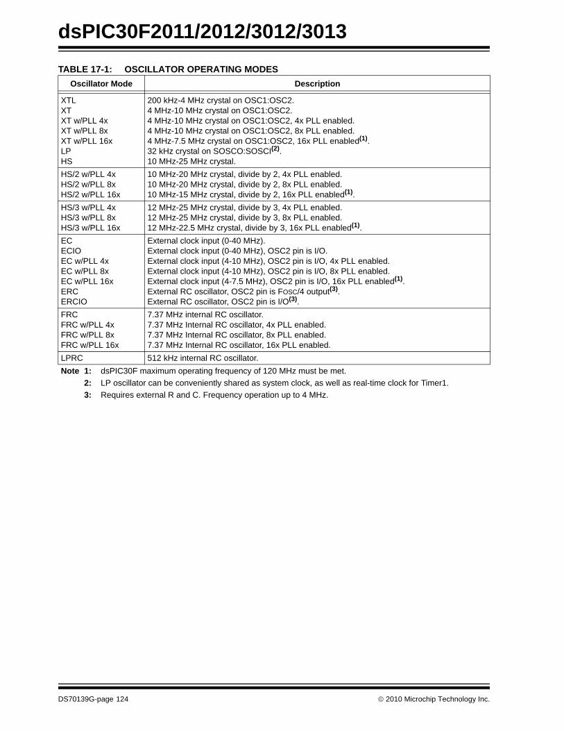
dsPIC30F2011/2012/3012/3013
TABLE 17-1: OSCILLATOR OPERATING MODESOscillator Mode Description
XTLXTXT w/PLL 4xXT w/PLL 8xXT w/PLL 16xLPHS
200 kHz-4 MHz crystal on OSC1:OSC2.4 MHz-10 MHz crystal on OSC1:OSC2. 4 MHz-10 MHz crystal on OSC1:OSC2, 4x PLL enabled.4 MHz-10 MHz crystal on OSC1:OSC2, 8x PLL enabled.4 MHz-7.5 MHz crystal on OSC1:OSC2, 16x PLL enabled(1).32 kHz crystal on SOSCO:SOSCI(2).10 MHz-25 MHz crystal.
HS/2 w/PLL 4xHS/2 w/PLL 8xHS/2 w/PLL 16x
10 MHz-20 MHz crystal, divide by 2, 4x PLL enabled.10 MHz-20 MHz crystal, divide by 2, 8x PLL enabled.10 MHz-15 MHz crystal, divide by 2, 16x PLL enabled(1).
HS/3 w/PLL 4xHS/3 w/PLL 8xHS/3 w/PLL 16x
12 MHz-25 MHz crystal, divide by 3, 4x PLL enabled.12 MHz-25 MHz crystal, divide by 3, 8x PLL enabled.12 MHz-22.5 MHz crystal, divide by 3, 16x PLL enabled(1).
ECECIOEC w/PLL 4xEC w/PLL 8xEC w/PLL 16xERCERCIO
External clock input (0-40 MHz).External clock input (0-40 MHz), OSC2 pin is I/O.External clock input (4-10 MHz), OSC2 pin is I/O, 4x PLL enabled.External clock input (4-10 MHz), OSC2 pin is I/O, 8x PLL enabled.External clock input (4-7.5 MHz), OSC2 pin is I/O, 16x PLL enabled(1).External RC oscillator, OSC2 pin is FOSC/4 output(3).External RC oscillator, OSC2 pin is I/O(3).
FRCFRC w/PLL 4xFRC w/PLL 8xFRC w/PLL 16x
7.37 MHz internal RC oscillator.7.37 MHz Internal RC oscillator, 4x PLL enabled.7.37 MHz Internal RC oscillator, 8x PLL enabled.7.37 MHz Internal RC oscillator, 16x PLL enabled.
LPRC 512 kHz internal RC oscillator. Note 1: dsPIC30F maximum operating frequency of 120 MHz must be met.
2: LP oscillator can be conveniently shared as system clock, as well as real-time clock for Timer1.3: Requires external R and C. Frequency operation up to 4 MHz.
DS70139G-page 124 © 2010 Microchip Technology Inc.
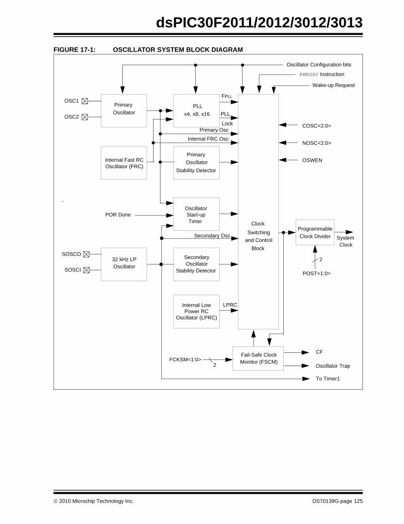
dsPIC30F2011/2012/3012/3013
FIGURE 17-1: OSCILLATOR SYSTEM BLOCK DIAGRAMPrimary OSC1
OSC2
SOSCO
SOSCI
Oscillator
32 kHz LP
Clock
and ControlBlock
Switching
Oscillator
x4, x8, x16 PLL
Primary Oscillator
Stability Detector
Stability Detector
SecondaryOscillator
ProgrammableClock Divider
OscillatorStart-upTimer
Fail-Safe ClockMonitor (FSCM)
Internal Fast RCOscillator (FRC)
Internal LowPower RC
Oscillator (LPRC)
PWRSAV Instruction
Wake-up Request
Oscillator Configuration bits
SystemClock
Oscillator Trap
To Timer1
LPRC
Secondary Osc
POR Done
Primary Osc
FPLL
POST<1:0>
2
FCKSM<1:0>2
PLL
Lock COSC<2:0>
NOSC<2:0>
OSWEN
CF
Internal FRC Osc
© 2010 Microchip Technology Inc. DS70139G-page 125
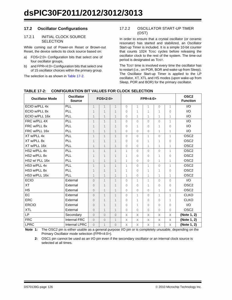
dsPIC30F2011/2012/3012/3013
17.2 Oscillator Configurations17.2.1 INITIAL CLOCK SOURCE SELECTION
While coming out of Power-on Reset or Brown-outReset, the device selects its clock source based on:
a) FOS<2:0> Configuration bits that select one offour oscillator groups,
b) and FPR<4:0> Configuration bits that select oneof 15 oscillator choices within the primary group.
The selection is as shown in Table 17-2.
17.2.2 OSCILLATOR START-UP TIMER (OST)
In order to ensure that a crystal oscillator (or ceramicresonator) has started and stabilized, an OscillatorStart-up Timer is included. It is a simple 10-bit counterthat counts 1024 TOSC cycles before releasing theoscillator clock to the rest of the system. The time-outperiod is designated as TOST.
The TOST time is involved every time the oscillator hasto restart (i.e., on POR, BOR and wake-up from Sleep).The Oscillator Start-up Timer is applied to the LPoscillator, XT, XTL and HS modes (upon wake-up fromSleep, POR and BOR) for the primary oscillator.
TABLE 17-2: CONFIGURATION BIT VALUES FOR CLOCK SELECTION
Oscillator Mode Oscillator Source FOS<2:0> FPR<4:0> OSC2
FunctionECIO w/PLL 4x PLL 1 1 1 0 1 1 0 1 I/OECIO w/PLL 8x PLL 1 1 1 0 1 1 1 0 I/OECIO w/PLL 16x PLL 1 1 1 0 1 1 1 1 I/OFRC w/PLL 4X PLL 1 1 1 0 0 0 0 1 I/OFRC w/PLL 8x PLL 1 1 1 0 1 0 1 0 I/OFRC w/PLL 16x PLL 1 1 1 0 0 0 1 1 I/OXT w/PLL 4x PLL 1 1 1 0 0 1 0 1 OSC2XT w/PLL 8x PLL 1 1 1 0 0 1 1 0 OSC2XT w/PLL 16x PLL 1 1 1 0 0 1 1 1 OSC2HS2 w/PLL 4x PLL 1 1 1 1 0 0 0 1 OSC2HS2 w/PLL 8x PLL 1 1 1 1 0 0 1 0 OSC2HS2 w/ PLL 16x PLL 1 1 1 1 0 0 1 1 OSC2HS3 w/PLL 4x PLL 1 1 1 1 0 1 0 1 OSC2HS3 w/PLL 8x PLL 1 1 1 1 0 1 1 0 OSC2HS3 w/PLL 16x PLL 1 1 1 1 0 1 1 1 OSC2ECIO External 0 1 1 0 1 1 0 0 I/OXT External 0 1 1 0 0 1 0 0 OSC2HS External 0 1 1 0 0 0 1 0 OSC2EC External 0 1 1 0 1 0 1 1 CLKOERC External 0 1 1 0 1 0 0 1 CLKOERCIO External 0 1 1 0 1 0 0 0 I/OXTL External 0 1 1 0 0 0 0 0 OSC2LP Secondary 0 0 0 X X X X X (Note 1, 2)FRC Internal FRC 0 0 1 X X X X X (Note 1, 2)LPRC Internal LPRC 0 1 0 X X X X X (Note 1, 2)Note 1: The OSC2 pin is either usable as a general purpose I/O pin or is completely unusable, depending on the
Primary Oscillator mode selection (FPR<4:0>).2: OSC1 pin cannot be used as an I/O pin even if the secondary oscillator or an internal clock source is
selected at all times.
DS70139G-page 126 © 2010 Microchip Technology Inc.
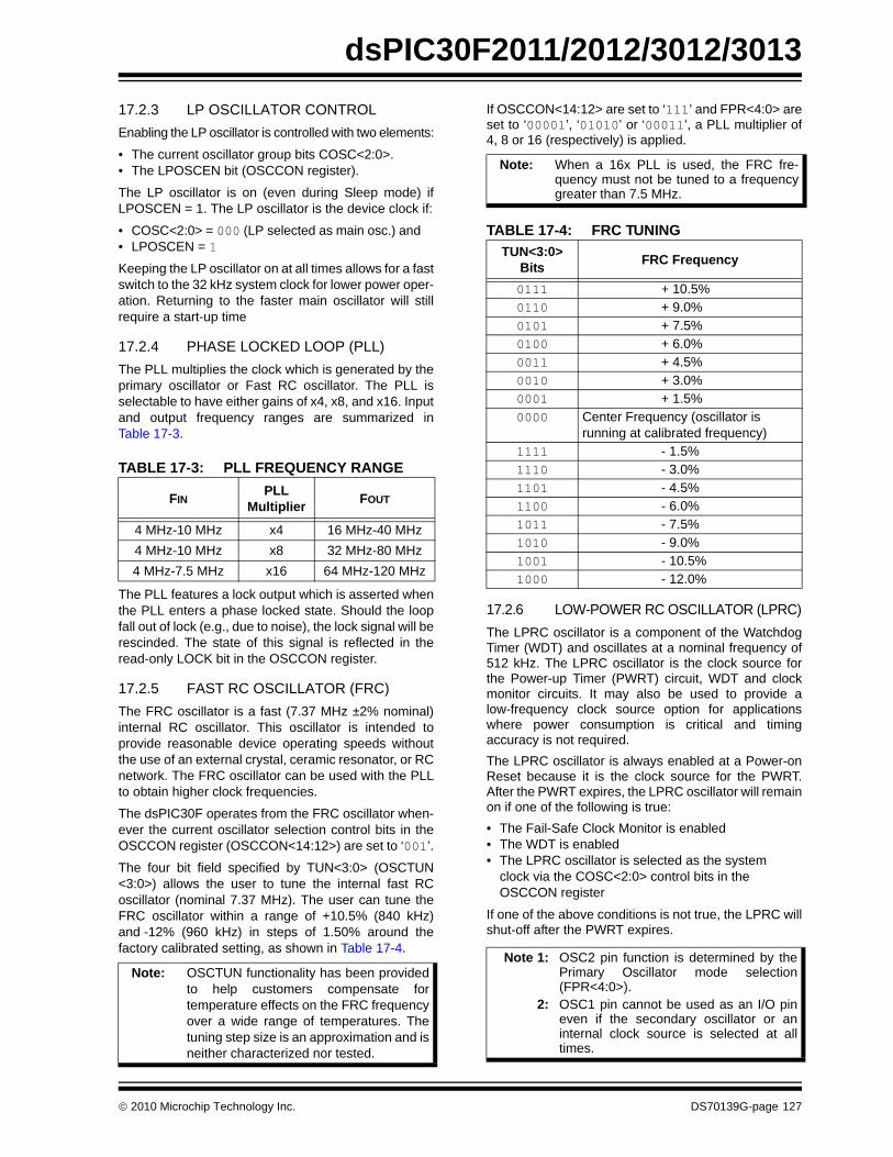
dsPIC30F2011/2012/3012/3013
17.2.3 LP OSCILLATOR CONTROLEnabling the LP oscillator is controlled with two elements:• The current oscillator group bits COSC<2:0>.• The LPOSCEN bit (OSCCON register).
The LP oscillator is on (even during Sleep mode) ifLPOSCEN = 1. The LP oscillator is the device clock if:
• COSC<2:0> = 000 (LP selected as main osc.) and• LPOSCEN = 1
Keeping the LP oscillator on at all times allows for a fastswitch to the 32 kHz system clock for lower power oper-ation. Returning to the faster main oscillator will stillrequire a start-up time
17.2.4 PHASE LOCKED LOOP (PLL)The PLL multiplies the clock which is generated by theprimary oscillator or Fast RC oscillator. The PLL isselectable to have either gains of x4, x8, and x16. Inputand output frequency ranges are summarized inTable 17-3.
TABLE 17-3: PLL FREQUENCY RANGE
The PLL features a lock output which is asserted whenthe PLL enters a phase locked state. Should the loopfall out of lock (e.g., due to noise), the lock signal will berescinded. The state of this signal is reflected in theread-only LOCK bit in the OSCCON register.
17.2.5 FAST RC OSCILLATOR (FRC)The FRC oscillator is a fast (7.37 MHz ±2% nominal)internal RC oscillator. This oscillator is intended toprovide reasonable device operating speeds withoutthe use of an external crystal, ceramic resonator, or RCnetwork. The FRC oscillator can be used with the PLLto obtain higher clock frequencies.
The dsPIC30F operates from the FRC oscillator when-ever the current oscillator selection control bits in theOSCCON register (OSCCON<14:12>) are set to ‘001’.
The four bit field specified by TUN<3:0> (OSCTUN<3:0>) allows the user to tune the internal fast RCoscillator (nominal 7.37 MHz). The user can tune theFRC oscillator within a range of +10.5% (840 kHz)and -12% (960 kHz) in steps of 1.50% around thefactory calibrated setting, as shown in Table 17-4.
If OSCCON<14:12> are set to ‘111’ and FPR<4:0> areset to ‘00001’, ‘01010’ or ‘00011’, a PLL multiplier of4, 8 or 16 (respectively) is applied.
TABLE 17-4: FRC TUNING
17.2.6 LOW-POWER RC OSCILLATOR (LPRC)The LPRC oscillator is a component of the WatchdogTimer (WDT) and oscillates at a nominal frequency of512 kHz. The LPRC oscillator is the clock source forthe Power-up Timer (PWRT) circuit, WDT and clockmonitor circuits. It may also be used to provide alow-frequency clock source option for applicationswhere power consumption is critical and timingaccuracy is not required.The LPRC oscillator is always enabled at a Power-onReset because it is the clock source for the PWRT.After the PWRT expires, the LPRC oscillator will remainon if one of the following is true:• The Fail-Safe Clock Monitor is enabled• The WDT is enabled• The LPRC oscillator is selected as the system
clock via the COSC<2:0> control bits in the OSCCON register
If one of the above conditions is not true, the LPRC willshut-off after the PWRT expires.
FINPLL
Multiplier FOUT
4 MHz-10 MHz x4 16 MHz-40 MHz4 MHz-10 MHz x8 32 MHz-80 MHz4 MHz-7.5 MHz x16 64 MHz-120 MHz
Note: OSCTUN functionality has been providedto help customers compensate fortemperature effects on the FRC frequencyover a wide range of temperatures. Thetuning step size is an approximation and isneither characterized nor tested.
Note: When a 16x PLL is used, the FRC fre-quency must not be tuned to a frequencygreater than 7.5 MHz.
TUN<3:0>Bits FRC Frequency
0111 + 10.5%0110 + 9.0%0101 + 7.5%0100 + 6.0%0011 + 4.5%0010 + 3.0%0001 + 1.5%0000 Center Frequency (oscillator is
running at calibrated frequency)1111 - 1.5%1110 - 3.0%1101 - 4.5%1100 - 6.0%1011 - 7.5%1010 - 9.0%1001 - 10.5%1000 - 12.0%
Note 1: OSC2 pin function is determined by thePrimary Oscillator mode selection(FPR<4:0>).
2: OSC1 pin cannot be used as an I/O pineven if the secondary oscillator or aninternal clock source is selected at alltimes.
© 2010 Microchip Technology Inc. DS70139G-page 127
dsPIC30F2011/2012/3012/3013
17.2.7 FAIL-SAFE CLOCK MONITORThe Fail-Safe Clock Monitor (FSCM) allows the deviceto continue to operate even in the event of an oscillatorfailure. The FSCM function is enabled by appropriatelyprogramming the FCKSM Configuration bits (clockswitch and monitor selection bits) in the FOSC DeviceConfiguration register. If the FSCM function is enabled,the LPRC internal oscillator will run at all times (exceptduring Sleep mode) and will not be subject to control bythe SWDTEN bit.In the event of an oscillator failure, the FSCM will gen-erate a clock failure trap event and will switch the sys-tem clock over to the FRC oscillator. The user will thenhave the option to either attempt to restart the oscillatoror execute a controlled shutdown. The user may decideto treat the trap as a warm Reset by simply loading theReset address into the oscillator fail trap vector. In thisevent, the CF (Clock Fail) bit (OSCCON<3>) is also setwhenever a clock failure is recognized.
In the event of a clock failure, the WDT is unaffectedand continues to run on the LPRC clock.
If the oscillator has a very slow start-up time coming outof POR, BOR or Sleep, it is possible that the PWRTtimer will expire before the oscillator has started. Insuch cases, the FSCM will be activated and the FSCMwill initiate a clock failure trap, and the COSC<2:0> bitsare loaded with FRC oscillator selection. This willeffectively shut-off the original oscillator that was tryingto start.
The user may detect this situation and restart theoscillator in the clock fail trap ISR.
Upon a clock failure detection, the FSCM module willinitiate a clock switch to the FRC oscillator as follows:
1. The COSC bits (OSCCON<14:12>) are loadedwith the FRC oscillator selection value.
2. CF bit is set (OSCCON<3>).3. OSWEN control bit (OSCCON<0>) is cleared.
For the purpose of clock switching, the clock sourcesare sectioned into four groups:
• Primary (with or without PLL)• Secondary• Internal FRC• Internal LPRC
The user can switch between these functional groupsbut cannot switch between options within a group. If theprimary group is selected, then the choice within thegroup is always determined by the FPR<4:0>Configuration bits.
The OSCCON register holds the Control and Statusbits related to clock switching.
• COSC<2:0>: Read-only bits always reflect the current oscillator group in effect.
• NOSC<2:0>: Control bits which are written to indicate the new oscillator group of choice.- On POR and BOR, COSC<2:0> and
NOSC<2:0> are both loaded with the Configuration bit values FOS<2:0>.
• LOCK: The LOCK bit indicates a PLL lock.• CF: Read-only bit indicating if a clock fail detect
has occurred.• OSWEN: Control bit changes from a ‘0’ to a ‘1’
when a clock transition sequence is initiated. Clearing the OSWEN control bit will abort a clock transition in progress (used for hang-up situations).
If Configuration bits FCKSM<1:0> = 1x, then the clockswitching and Fail-Safe Clock monitoring functions aredisabled. This is the default Configuration bit setting.
If clock switching is disabled, then the FOS<2:0> andFPR<4:0> bits directly control the oscillator selectionand the COSC<2:0> bits do not control the clock selec-tion. However, these bits will reflect the clock sourceselection.
17.2.8 PROTECTION AGAINST ACCIDENTAL WRITES TO OSCCON
A write to the OSCCON register is intentionally madedifficult because it controls clock switching and clockscaling.
To write to the OSCCON low byte, the following codesequence must be executed without any otherinstructions in between:
Byte Write 0x46 to OSCCON lowByte Write 0x57 to OSCCON low
Byte write is allowed for one instruction cycle. Write thedesired value or use bit manipulation instruction.
To write to the OSCCON high byte, the followinginstructions must be executed without any otherinstructions in between:
Byte Write 0x78 to OSCCON highByte Write 0x9A to OSCCON high
Byte write is allowed for one instruction cycle. Write thedesired value or use bit manipulation instruction.
Note: The application should not attempt toswitch to a clock of frequency lower than100 kHz when the Fail-Safe Clock Monitoris enabled. If such clock switching isperformed, the device may generate anoscillator fail trap and switch to the FastRC oscillator.
DS70139G-page 128 © 2010 Microchip Technology Inc.
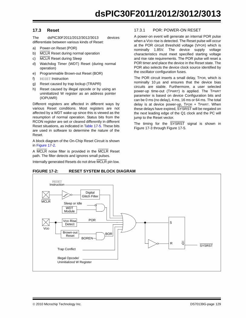
dsPIC30F2011/2012/3012/3013
17.3 ResetThe dsPIC30F2011/2012/3012/3013 devicesdifferentiate between various kinds of Reset:a) Power-on Reset (POR) b) MCLR Reset during normal operationc) MCLR Reset during Sleep d) Watchdog Timer (WDT) Reset (during normal
operation)e) Programmable Brown-out Reset (BOR) f) RESET Instructiong) Reset caused by trap lockup (TRAPR)h) Reset caused by illegal opcode or by using an
uninitialized W register as an address pointer(IOPUWR)
Different registers are affected in different ways byvarious Reset conditions. Most registers are notaffected by a WDT wake-up since this is viewed as theresumption of normal operation. Status bits from theRCON register are set or cleared differently in differentReset situations, as indicated in Table 17-5. These bitsare used in software to determine the nature of theReset.
A block diagram of the On-Chip Reset Circuit is shownin Figure 17-2.
A MCLR noise filter is provided in the MCLR Resetpath. The filter detects and ignores small pulses.
Internally generated Resets do not drive MCLR pin low.
17.3.1 POR: POWER-ON RESETA power-on event will generate an internal POR pulsewhen a VDD rise is detected. The Reset pulse will occurat the POR circuit threshold voltage (VPOR) which isnominally 1.85V. The device supply voltagecharacteristics must meet specified starting voltageand rise rate requirements. The POR pulse will reset aPOR timer and place the device in the Reset state. ThePOR also selects the device clock source identified bythe oscillator configuration fuses.
The POR circuit inserts a small delay, TPOR, which isnominally 10 μs and ensures that the device biascircuits are stable. Furthermore, a user selectedpower-up time-out (TPWRT) is applied. The TPWRTparameter is based on device Configuration bits andcan be 0 ms (no delay), 4 ms, 16 ms or 64 ms. The totaldelay is at device power-up, TPOR + TPWRT. Whenthese delays have expired, SYSRST will be negated onthe next leading edge of the Q1 clock and the PC willjump to the Reset vector.
The timing for the SYSRST signal is shown inFigure 17-3 through Figure 17-5.
FIGURE 17-2: RESET SYSTEM BLOCK DIAGRAM
S
R Q
MCLR
VDD
VDD RiseDetect
POR
SYSRST
Sleep or Idle
Brown-outReset
BOREN
RESETInstruction
WDTModule
DigitalGlitch Filter
BOR
Trap Conflict
Illegal Opcode/Uninitialized W Register
© 2010 Microchip Technology Inc. DS70139G-page 129
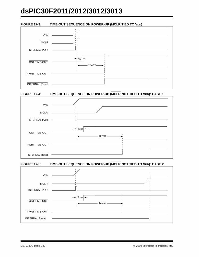
dsPIC30F2011/2012/3012/3013
FIGURE 17-3: TIME-OUT SEQUENCE ON POWER-UP (MCLR TIED TO VDD)FIGURE 17-4: TIME-OUT SEQUENCE ON POWER-UP (MCLR NOT TIED TO VDD): CASE 1
FIGURE 17-5: TIME-OUT SEQUENCE ON POWER-UP (MCLR NOT TIED TO VDD): CASE 2
TPWRT
TOST
VDD
INTERNAL POR
PWRT TIME-OUT
OST TIME-OUT
INTERNAL Reset
MCLR
TPWRT
TOST
VDD
INTERNAL POR
PWRT TIME-OUT
OST TIME-OUT
INTERNAL Reset
MCLR
VDD
MCLR
INTERNAL POR
PWRT TIME-OUT
OST TIME-OUT
INTERNAL Reset
TPWRT
TOST
DS70139G-page 130 © 2010 Microchip Technology Inc.
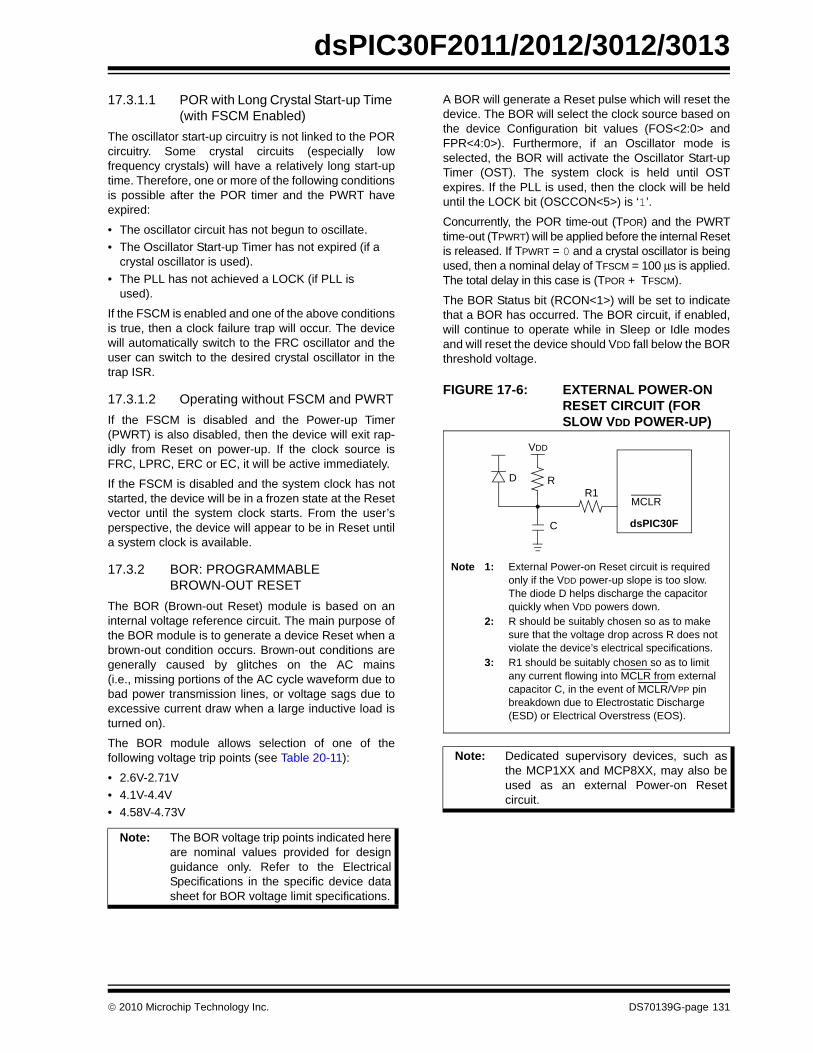
dsPIC30F2011/2012/3012/3013
17.3.1.1 POR with Long Crystal Start-up Time(with FSCM Enabled)The oscillator start-up circuitry is not linked to the PORcircuitry. Some crystal circuits (especially lowfrequency crystals) will have a relatively long start-uptime. Therefore, one or more of the following conditionsis possible after the POR timer and the PWRT haveexpired:
• The oscillator circuit has not begun to oscillate.• The Oscillator Start-up Timer has not expired (if a
crystal oscillator is used).• The PLL has not achieved a LOCK (if PLL is
used).
If the FSCM is enabled and one of the above conditionsis true, then a clock failure trap will occur. The devicewill automatically switch to the FRC oscillator and theuser can switch to the desired crystal oscillator in thetrap ISR.
17.3.1.2 Operating without FSCM and PWRTIf the FSCM is disabled and the Power-up Timer(PWRT) is also disabled, then the device will exit rap-idly from Reset on power-up. If the clock source isFRC, LPRC, ERC or EC, it will be active immediately.
If the FSCM is disabled and the system clock has notstarted, the device will be in a frozen state at the Resetvector until the system clock starts. From the user’sperspective, the device will appear to be in Reset untila system clock is available.
17.3.2 BOR: PROGRAMMABLE BROWN-OUT RESET
The BOR (Brown-out Reset) module is based on aninternal voltage reference circuit. The main purpose ofthe BOR module is to generate a device Reset when abrown-out condition occurs. Brown-out conditions aregenerally caused by glitches on the AC mains(i.e., missing portions of the AC cycle waveform due tobad power transmission lines, or voltage sags due toexcessive current draw when a large inductive load isturned on).
The BOR module allows selection of one of thefollowing voltage trip points (see Table 20-11):
• 2.6V-2.71V• 4.1V-4.4V• 4.58V-4.73V
A BOR will generate a Reset pulse which will reset thedevice. The BOR will select the clock source based onthe device Configuration bit values (FOS<2:0> andFPR<4:0>). Furthermore, if an Oscillator mode isselected, the BOR will activate the Oscillator Start-upTimer (OST). The system clock is held until OSTexpires. If the PLL is used, then the clock will be helduntil the LOCK bit (OSCCON<5>) is ‘1’.
Concurrently, the POR time-out (TPOR) and the PWRTtime-out (TPWRT) will be applied before the internal Resetis released. If TPWRT = 0 and a crystal oscillator is beingused, then a nominal delay of TFSCM = 100 μs is applied.The total delay in this case is (TPOR + TFSCM).
The BOR Status bit (RCON<1>) will be set to indicatethat a BOR has occurred. The BOR circuit, if enabled,will continue to operate while in Sleep or Idle modesand will reset the device should VDD fall below the BORthreshold voltage.
FIGURE 17-6: EXTERNAL POWER-ON RESET CIRCUIT (FOR SLOW VDD POWER-UP)
Note: The BOR voltage trip points indicated hereare nominal values provided for designguidance only. Refer to the ElectricalSpecifications in the specific device datasheet for BOR voltage limit specifications.
Note: Dedicated supervisory devices, such asthe MCP1XX and MCP8XX, may also beused as an external Power-on Resetcircuit.
Note 1: External Power-on Reset circuit is required only if the VDD power-up slope is too slow. The diode D helps discharge the capacitor quickly when VDD powers down.
2: R should be suitably chosen so as to make sure that the voltage drop across R does not violate the device’s electrical specifications.
3: R1 should be suitably chosen so as to limit any current flowing into MCLR from external capacitor C, in the event of MCLR/VPP pin breakdown due to Electrostatic Discharge (ESD) or Electrical Overstress (EOS).
C
R1RD
VDD
dsPIC30F
MCLR
© 2010 Microchip Technology Inc. DS70139G-page 131
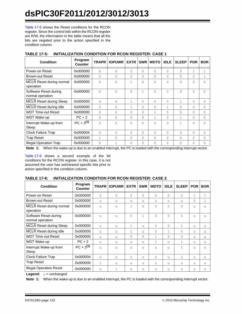
dsPIC30F2011/2012/3012/3013
Table 17-5 shows the Reset conditions for the RCONregister. Since the control bits within the RCON registerare R/W, the information in the table means that all thebits are negated prior to the action specified in thecondition column.TABLE 17-5: INITIALIZATION CONDITION FOR RCON REGISTER: CASE 1
Table 17-6 shows a second example of the bitconditions for the RCON register. In this case, it is notassumed the user has set/cleared specific bits prior toaction specified in the condition column.
TABLE 17-6: INITIALIZATION CONDITION FOR RCON REGISTER: CASE 2
Condition Program Counter TRAPR IOPUWR EXTR SWR WDTO IDLE SLEEP POR BOR
Power-on Reset 0x000000 0 0 0 0 0 0 0 1 1
Brown-out Reset 0x000000 0 0 0 0 0 0 0 0 1
MCLR Reset during normaloperation
0x000000 0 0 1 0 0 0 0 0 0
Software Reset during normal operation
0x000000 0 0 0 1 0 0 0 0 0
MCLR Reset during Sleep 0x000000 0 0 1 0 0 0 1 0 0
MCLR Reset during Idle 0x000000 0 0 1 0 0 1 0 0 0
WDT Time-out Reset 0x000000 0 0 0 0 1 0 0 0 0
WDT Wake-up PC + 2 0 0 0 0 1 0 1 0 0
Interrupt Wake-up from Sleep
PC + 2(1) 0 0 0 0 0 0 1 0 0
Clock Failure Trap 0x000004 0 0 0 0 0 0 0 0 0
Trap Reset 0x000000 1 0 0 0 0 0 0 0 0
Illegal Operation Trap 0x000000 0 1 0 0 0 0 0 0 0
Note 1: When the wake-up is due to an enabled interrupt, the PC is loaded with the corresponding interrupt vector.
Condition Program Counter TRAPR IOPUWR EXTR SWR WDTO IDLE SLEEP POR BOR
Power-on Reset 0x000000 0 0 0 0 0 0 0 1 1
Brown-out Reset 0x000000 u u u u u u u 0 1
MCLR Reset during normal operation
0x000000 u u 1 0 0 0 0 u u
Software Reset during normal operation
0x000000 u u 0 1 0 0 0 u u
MCLR Reset during Sleep 0x000000 u u 1 u 0 0 1 u u
MCLR Reset during Idle 0x000000 u u 1 u 0 1 0 u u
WDT Time-out Reset 0x000000 u u 0 0 1 0 0 u u
WDT Wake-up PC + 2 u u u u 1 u 1 u u
Interrupt Wake-up from Sleep
PC + 2(1) u u u u u u 1 u u
Clock Failure Trap 0x000004 u u u u u u u u u
Trap Reset 0x000000 1 u u u u u u u u
Illegal Operation Reset 0x000000 u 1 u u u u u u u
Legend: u = unchangedNote 1: When the wake-up is due to an enabled interrupt, the PC is loaded with the corresponding interrupt vector.
DS70139G-page 132 © 2010 Microchip Technology Inc.
dsPIC30F2011/2012/3012/3013
17.4 Watchdog Timer (WDT)17.4.1 WATCHDOG TIMER OPERATIONThe primary function of the Watchdog Timer (WDT) isto reset the processor in the event of a softwaremalfunction. The WDT is a free-running timer whichruns off an on-chip RC oscillator, requiring no externalcomponent. Therefore, the WDT timer will continue tooperate even if the main processor clock (e.g., thecrystal oscillator) fails.
17.4.2 ENABLING AND DISABLING THE WDT
The Watchdog Timer can be “Enabled” or “Disabled”only through a Configuration bit (FWDTEN) in theConfiguration register, FWDT.
Setting FWDTEN = 1 enables the Watchdog Timer. Theenabling is done when programming the device. Bydefault, after chip erase, FWDTEN bit = 1. Any deviceprogrammer capable of programming dsPIC30Fdevices allows programming of this and otherConfiguration bits.
If enabled, the WDT will increment until it overflows or“times out”. A WDT time-out will force a device Reset(except during Sleep). To prevent a WDT time-out, theuser must clear the Watchdog Timer using a CLRWDTinstruction.
If a WDT times out during Sleep, the device willwake-up. The WDTO bit in the RCON register will becleared to indicate a wake-up resulting from a WDTtime-out.
Setting FWDTEN = 0 allows user software toenable/disable the Watchdog Timer via the SWDTEN(RCON<5>) control bit.
17.5 Low-Voltage DetectThe Low-Voltage Detect (LVD) module is used todetect when the VDD of the device drops below athreshold value, VLVD, which is determined by theLVDL<3:0> bits (RCON<11:8>) and is thus user pro-grammable. The internal voltage reference circuitryrequires a nominal amount of time to stabilize, and theBGST bit (RCON<13>) indicates when the voltagereference has stabilized.
In some devices, the LVD threshold voltage may beapplied externally on the LVDIN pin.
The LVD module is enabled by setting the LVDEN bit(RCON<12>).
17.6 Power-Saving ModesThere are two power-saving states that can be enteredthrough the execution of a special instruction, PWRSAV;these are Sleep and Idle.
The format of the PWRSAV instruction is as follows:
PWRSAV <parameter>, where ‘parameter’ definesIdle or Sleep mode.
17.6.1 SLEEP MODE In Sleep mode, the clock to the CPU and peripherals isshut down. If an on-chip oscillator is being used, it isshut down.
The Fail-Safe Clock Monitor is not functional duringSleep since there is no clock to monitor. However,LPRC clock remains active if WDT is operational duringSleep.
The brown-out protection circuit and the Low-VoltageDetect circuit, if enabled, will remain functional duringSleep.
The processor wakes up from Sleep if at least one ofthe following conditions has occurred:
• any interrupt that is individually enabled and meets the required priority level
• any Reset (POR, BOR and MCLR) • WDT time-out
On waking up from Sleep mode, the processor willrestart the same clock that was active prior to entry intoSleep mode. When clock switching is enabled, bitsCOSC<2:0> will determine the oscillator source thatwill be used on wake-up. If clock switch is disabled,then there is only one system clock.
If the clock source is an oscillator, the clock to thedevice will be held off until OST times out (indicating astable oscillator). If PLL is used, the system clock isheld off until LOCK = 1 (indicating that the PLL isstable). In either case, TPOR, TLOCK and TPWRT delaysare applied.
If EC, FRC, LPRC or ERC oscillators are used, then adelay of TPOR (~ 10 μs) is applied. This is the smallestdelay possible on wake-up from Sleep.
Moreover, if LP oscillator was active during Sleep andLP is the oscillator used on wake-up, then the start-updelay will be equal to TPOR. PWRT delay and OSTtimer delay are not applied. In order to have thesmallest possible start-up delay when waking up fromSleep, one of these faster wake-up options should beselected before entering Sleep.
Note: If a POR or BOR occurred, the selection ofthe oscillator is based on the FOS<2:0>and FPR<4:0> Configuration bits.
© 2010 Microchip Technology Inc. DS70139G-page 133
dsPIC30F2011/2012/3012/3013
Any interrupt that is individually enabled (using thecorresponding IE bit) and meets the prevailing prioritylevel will be able to wake-up the processor. Theprocessor will process the interrupt and branch to theISR. The Sleep Status bit in the RCON register is setupon wake-up.All Resets will wake-up the processor from Sleepmode. Any Reset, other than POR, will set the SleepStatus bit. In a POR, the Sleep bit is cleared.
If the Watchdog Timer is enabled, then the processorwill wake-up from Sleep mode upon WDT time-out. TheSleep and WDTO Status bits are both set.
17.6.2 IDLE MODEIn Idle mode, the clock to the CPU is shut down whileperipherals keep running. Unlike Sleep mode, the clocksource remains active.
Several peripherals have a control bit in each modulethat allows them to operate during Idle.
LPRC Fail-Safe Clock remains active if clock failuredetect is enabled.
The processor wakes up from Idle if at least one of thefollowing conditions has occurred:
• any interrupt that is individually enabled (IE bit is ‘1’) and meets the required priority level
• any Reset (POR, BOR, MCLR)• WDT time-out
Upon wake-up from Idle mode, the clock is re-appliedto the CPU and instruction execution beginsimmediately, starting with the instruction following thePWRSAV instruction.
Any interrupt that is individually enabled (using IE bit)and meets the prevailing priority level will be able towake-up the processor. The processor will process theinterrupt and branch to the ISR. The Idle Status bit inthe RCON register is set upon wake-up.
Any Reset other than POR will set the Idle Status bit.On a POR, the Idle bit is cleared.
If Watchdog Timer is enabled, then the processor willwake-up from Idle mode upon WDT time-out. The Idleand WDTO Status bits are both set.
Unlike wake-up from Sleep, there are no time delaysinvolved in wake-up from Idle.
17.7 Device Configuration RegistersThe Configuration bits in each device Configurationregister specify some of the device modes and areprogrammed by a device programmer, or by using theIn-Circuit Serial Programming™ (ICSP™) feature ofthe device. Each device Configuration register is a24-bit register, but only the lower 16 bits of eachregister are used to hold configuration data. There arefive device Configuration registers available to theuser:
1. FOSC (0xF80000): Oscillator Configuration Register
2. FWDT (0xF80002): Watchdog Timer Configuration Register
3. FBORPOR (0xF80004): BOR and POR Configuration Register
4. FGS (0xF8000A): General Code Segment Configuration Register
5. FICD (0xF8000C): Debug Configuration Register
The placement of the Configuration bits isautomatically handled when you select the device inyour device programmer. The desired state of theConfiguration bits may be specified in the source code(dependent on the language tool used), or through theprogramming interface. After the device has beenprogrammed, the application software may read theConfiguration bit values through the table readinstructions. For additional information, please refer tothe Programming Specifications of the device.
Note: In spite of various delays applied (TPOR,TLOCK and TPWRT), the crystal oscillator(and PLL) may not be active at the end ofthe time-out (e.g., for low-frequencycrystals). In such cases, if FSCM isenabled, then the device will detect this asa clock failure and process the clock failuretrap, the FRC oscillator will be enabled andthe user will have to re-enable the crystaloscillator. If FSCM is not enabled, then thedevice will simply suspend execution ofcode until the clock is stable and will remainin Sleep until the oscillator clock hasstarted.
Note: If the code protection Configuration fusebits (FGS<GCP> and FGS<GWRP>)have been programmed, an erase of theentire code-protected device is onlypossible at voltages VDD ≥ 4.5V.
DS70139G-page 134 © 2010 Microchip Technology Inc.
dsPIC30F2011/2012/3012/3013
17.8 Peripheral Module Disable (PMD)RegistersThe Peripheral Module Disable (PMD) registersprovide a method to disable a peripheral module bystopping all clock sources supplied to that module.When a peripheral is disabled via the appropriate PMDcontrol bit, the peripheral is in a minimum powerconsumption state. The Control and Status registersassociated with the peripheral will also be disabled sowrites to those registers will have no effect and readvalues will be invalid.
A peripheral module will only be enabled if both theassociated bit in the PMD register is cleared and theperipheral is supported by the specific dsPIC DSCvariant. If the peripheral is present in the device, it isenabled in the PMD register by default.
17.9 In-Circuit DebuggerWhen MPLAB® ICD 2 is selected as a Debugger, theIn-Circuit Debugging functionality is enabled. Thisfunction allows simple debugging functions when usedwith MPLAB IDE. When the device has this featureenabled, some of the resources are not available forgeneral use. These resources include the first 80 bytesof Data RAM and two I/O pins.
One of four pairs of Debug I/O pins may be selected bythe user using configuration options in MPLAB IDE.These pin pairs are named EMUD/EMUC,EMUD1/EMUC1, EMUD2/EMUC2 andEMUD3/EMUC3.
In each case, the selected EMUD pin is theEmulation/Debug Data line, and the EMUC pin is theEmulation/Debug Clock line. These pins will interfaceto the MPLAB ICD 2 module available from Microchip.The selected pair of Debug I/O pins is used by MPLABICD 2 to send commands and receive responses, aswell as to send and receive data. To use the In-CircuitDebugger function of the device, the design mustimplement ICSP connections to MCLR, VDD, VSS,PGC, PGD and the selected EMUDx/EMUCx pin pair.
This gives rise to two possibilities:
1. If EMUD/EMUC is selected as the Debug I/O pinpair, then only a 5-pin interface is required, asthe EMUD and EMUC pin functions are multi-plexed with the PGD and PGC pin functions inall dsPIC30F devices.
2. If EMUD1/EMUC1, EMUD2/EMUC2 orEMUD3/EMUC3 is selected as the Debug I/Opin pair, then a 7-pin interface is required, as theEMUDx/EMUCx pin functions (x = 1, 2 or 3) arenot multiplexed with the PGD and PGC pinfunctions.
Note 1: If a PMD bit is set, the correspondingmodule is disabled after a delay of 1instruction cycle. Similarly, if a PMD bit iscleared, the corresponding module isenabled after a delay of 1 instructioncycle (assuming the module Control reg-isters are already configured to enablemodule operation).
2: In dsPIC30F2011, dsPIC30F3012 anddsPIC30F2012 devices, the U2MD bit isreadable and writable and will be read as‘1’ when set.
© 2010 Microchip Technology Inc. DS70139G-page 135
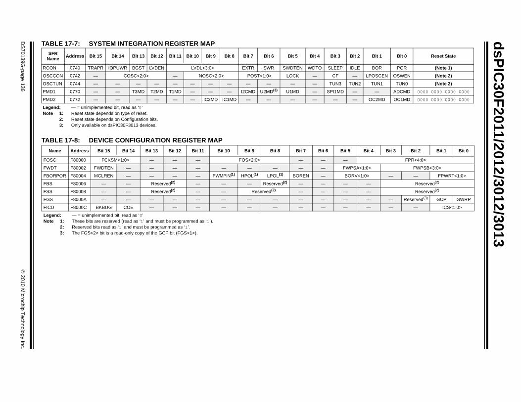
dsPIC30F2011/2012/3012/3013
DS
70139G-page 136
© 2010 M
icrochip Technology Inc.
2 Bit 1 Bit 0 Reset State
E BOR POR (Note 1)LPOSCEN OSWEN (Note 2)
2 TUN1 TUN0 (Note 2)— ADCMD 0000 0000 0000 0000
OC2MD OC1MD 0000 0000 0000 0000
Bit 4 Bit 3 Bit 2 Bit 1 Bit 0
FPR<4:0>
A<1:0> FWPSB<3:0>
<1:0> — — FPWRT<1:0>
— Reserved(2)
— Reserved(2)
— — Reserved(3) GCP GWRP
— — — ICS<1:0>
TABLE 17-7: SYSTEM INTEGRATION REGISTER MAP
TABLE 17-8: DEVICE CONFIGURATION REGISTER MAP
SFR Name Address Bit 15 Bit 14 Bit 13 Bit 12 Bit 11 Bit 10 Bit 9 Bit 8 Bit 7 Bit 6 Bit 5 Bit 4 Bit 3 Bit
RCON 0740 TRAPR IOPUWR BGST LVDEN LVDL<3:0> EXTR SWR SWDTEN WDTO SLEEP IDL
OSCCON 0742 — COSC<2:0> — NOSC<2:0> POST<1:0> LOCK — CF —
OSCTUN 0744 — — — — — — — — — — — — TUN3 TUN
PMD1 0770 — — T3MD T2MD T1MD — — — I2CMD U2MD(3) U1MD — SPI1MD —
PMD2 0772 — — — — — — IC2MD IC1MD — — — — — —
Legend: — = unimplemented bit, read as ‘0’Note 1: Reset state depends on type of reset.
2: Reset state depends on Configuration bits.3: Only available on dsPIC30F3013 devices.
Name Address Bit 15 Bit 14 Bit 13 Bit 12 Bit 11 Bit 10 Bit 9 Bit 8 Bit 7 Bit 6 Bit 5
FOSC F80000 FCKSM<1:0> — — — FOS<2:0> — — —
FWDT F80002 FWDTEN — — — — — — — — — FWPS
FBORPOR F80004 MCLREN — — — — PWMPIN(1) HPOL(1) LPOL(1) BOREN — BORV
FBS F80006 — — Reserved(2) — — — Reserved(2) — — —
FSS F80008 — — Reserved(2) — — Reserved(2) — — —
FGS F8000A — — — — — — — — — — —
FICD F8000C BKBUG COE — — — — — — — — —
Legend: — = unimplemented bit, read as ‘0’Note 1: These bits are reserved (read as ‘1’ and must be programmed as ‘1’).
2: Reserved bits read as ‘1’ and must be programmed as ‘1’.3: The FGS<2> bit is a read-only copy of the GCP bit (FGS<1>).
dsPIC30F2011/2012/3012/3013
18.0 INSTRUCTION SET SUMMARY
The dsPIC30F instruction set adds manyenhancements to the previous PIC® MCU instructionsets, while maintaining an easy migration from PICMCU instruction sets.
Most instructions are a single program memory word(24 bits). Only three instructions require two programmemory locations.
Each single-word instruction is a 24-bit word dividedinto an 8-bit opcode which specifies the instructiontype, and one or more operands which further specifythe operation of the instruction.
The instruction set is highly orthogonal and is groupedinto five basic categories:
• Word or byte-oriented operations• Bit-oriented operations• Literal operations• DSP operations• Control operations
Table 18-1 shows the general symbols used indescribing the instructions.
The dsPIC30F instruction set summary in Table 18-2lists all the instructions, along with the status flagsaffected by each instruction.
Most word or byte-oriented W register instructions(including barrel shift instructions) have threeoperands:
• The first source operand which is typically a register ‘Wb’ without any address modifier
• The second source operand which is typically a register ‘Ws’ with or without an address modifier
• The destination of the result which is typically a register ‘Wd’ with or without an address modifier
However, word or byte-oriented file register instructionshave two operands:
• The file register specified by the value ‘f’• The destination, which could either be the file
register ‘f’ or the W0 register, which is denoted as ‘WREG’
Most bit-oriented instructions (including simplerotate/shift instructions) have two operands:
• The W register (with or without an address modifier) or file register (specified by the value of ‘Ws’ or ‘f’)
• The bit in the W register or file register (specified by a literal value or indirectly by the contents of register ‘Wb’)
The literal instructions that involve data movement mayuse some of the following operands:
• A literal value to be loaded into a W register or file register (specified by the value of ‘k’)
• The W register or file register where the literal value is to be loaded (specified by ‘Wb’ or ‘f’)
However, literal instructions that involve arithmetic orlogical operations use some of the following operands:
• The first source operand which is a register ‘Wb’ without any address modifier
• The second source operand which is a literal value
• The destination of the result (only if not the same as the first source operand) which is typically a register ‘Wd’ with or without an address modifier
The MAC class of DSP instructions may use some of thefollowing operands:
• The accumulator (A or B) to be used (required operand)
• The W registers to be used as the two operands• The X and Y address space prefetch operations• The X and Y address space prefetch destinations• The accumulator write-back destination
The other DSP instructions do not involve anymultiplication, and may include:
• The accumulator to be used (required)• The source or destination operand (designated as
Wso or Wdo, respectively) with or without an address modifier
• The amount of shift specified by a W register ‘Wn’ or a literal value
The control instructions may use some of the followingoperands:
• A program memory address • The mode of the table read and table write
instructions
Note: This data sheet summarizes features ofthis group of dsPIC30F devices and is notintended to be a complete referencesource. For more information on the CPU,peripherals, register descriptions andgeneral device functionality, refer to the“dsPIC30F Family Reference Manual”(DS70046). For more information on thedevice instruction set and programming,refer to the “dsPIC30F Programmer’sReference Manual” (DS70030).
© 2010 Microchip Technology Inc. DS70139G-page 137
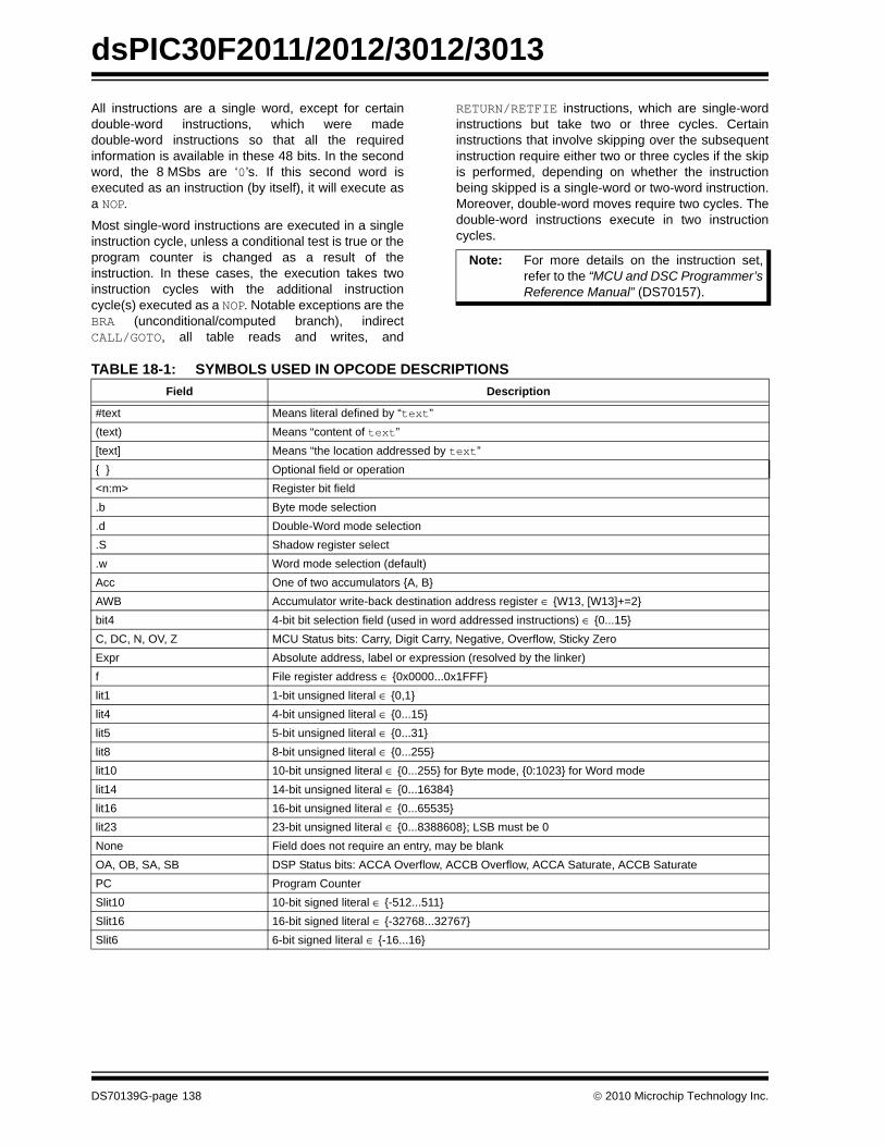
dsPIC30F2011/2012/3012/3013
All instructions are a single word, except for certaindouble-word instructions, which were madedouble-word instructions so that all the requiredinformation is available in these 48 bits. In the secondword, the 8 MSbs are ‘0’s. If this second word isexecuted as an instruction (by itself), it will execute asa NOP.Most single-word instructions are executed in a singleinstruction cycle, unless a conditional test is true or theprogram counter is changed as a result of theinstruction. In these cases, the execution takes twoinstruction cycles with the additional instructioncycle(s) executed as a NOP. Notable exceptions are theBRA (unconditional/computed branch), indirectCALL/GOTO, all table reads and writes, and
RETURN/RETFIE instructions, which are single-wordinstructions but take two or three cycles. Certaininstructions that involve skipping over the subsequentinstruction require either two or three cycles if the skipis performed, depending on whether the instructionbeing skipped is a single-word or two-word instruction.Moreover, double-word moves require two cycles. Thedouble-word instructions execute in two instructioncycles.
Note: For more details on the instruction set,refer to the “MCU and DSC Programmer’sReference Manual” (DS70157).
TABLE 18-1: SYMBOLS USED IN OPCODE DESCRIPTIONSField Description
#text Means literal defined by “text”(text) Means “content of text”[text] Means “the location addressed by text”{ } Optional field or operation<n:m> Register bit field.b Byte mode selection.d Double-Word mode selection.S Shadow register select.w Word mode selection (default)Acc One of two accumulators {A, B}AWB Accumulator write-back destination address register ∈ {W13, [W13]+=2}bit4 4-bit bit selection field (used in word addressed instructions) ∈ {0...15}C, DC, N, OV, Z MCU Status bits: Carry, Digit Carry, Negative, Overflow, Sticky ZeroExpr Absolute address, label or expression (resolved by the linker)f File register address ∈ {0x0000...0x1FFF}lit1 1-bit unsigned literal ∈ {0,1}lit4 4-bit unsigned literal ∈ {0...15}lit5 5-bit unsigned literal ∈ {0...31}lit8 8-bit unsigned literal ∈ {0...255}lit10 10-bit unsigned literal ∈ {0...255} for Byte mode, {0:1023} for Word modelit14 14-bit unsigned literal ∈ {0...16384}lit16 16-bit unsigned literal ∈ {0...65535}lit23 23-bit unsigned literal ∈ {0...8388608}; LSB must be 0None Field does not require an entry, may be blankOA, OB, SA, SB DSP Status bits: ACCA Overflow, ACCB Overflow, ACCA Saturate, ACCB SaturatePC Program CounterSlit10 10-bit signed literal ∈ {-512...511}Slit16 16-bit signed literal ∈ {-32768...32767}Slit6 6-bit signed literal ∈ {-16...16}
DS70139G-page 138 © 2010 Microchip Technology Inc.
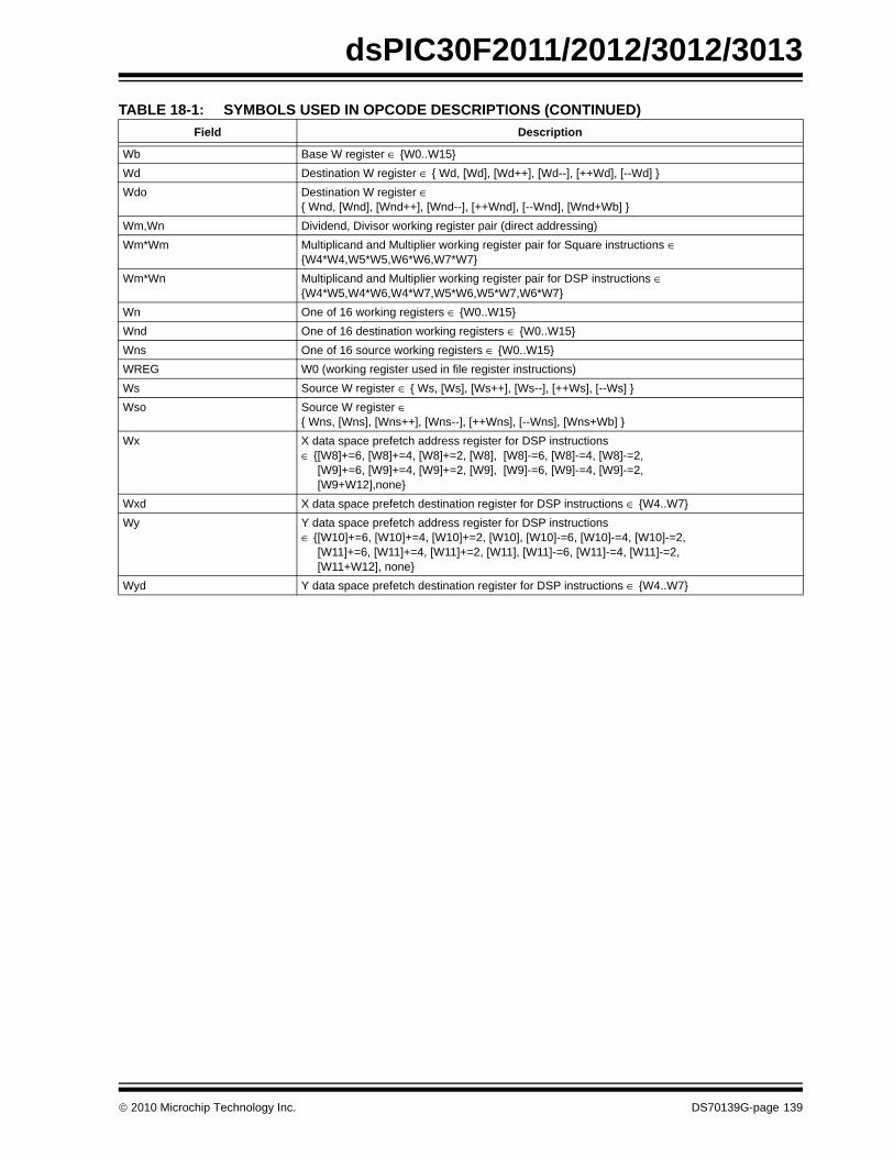
dsPIC30F2011/2012/3012/3013
Wb Base W register ∈ {W0..W15}Wd Destination W register ∈ { Wd, [Wd], [Wd++], [Wd--], [++Wd], [--Wd] }Wdo Destination W register ∈
{ Wnd, [Wnd], [Wnd++], [Wnd--], [++Wnd], [--Wnd], [Wnd+Wb] } Wm,Wn Dividend, Divisor working register pair (direct addressing)Wm*Wm Multiplicand and Multiplier working register pair for Square instructions ∈
{W4*W4,W5*W5,W6*W6,W7*W7} Wm*Wn Multiplicand and Multiplier working register pair for DSP instructions ∈
{W4*W5,W4*W6,W4*W7,W5*W6,W5*W7,W6*W7}Wn One of 16 working registers ∈ {W0..W15}Wnd One of 16 destination working registers ∈ {W0..W15}Wns One of 16 source working registers ∈ {W0..W15}WREG W0 (working register used in file register instructions)Ws Source W register ∈ { Ws, [Ws], [Ws++], [Ws--], [++Ws], [--Ws] }Wso Source W register ∈
{ Wns, [Wns], [Wns++], [Wns--], [++Wns], [--Wns], [Wns+Wb] } Wx X data space prefetch address register for DSP instructions
∈ {[W8]+=6, [W8]+=4, [W8]+=2, [W8], [W8]-=6, [W8]-=4, [W8]-=2, [W9]+=6, [W9]+=4, [W9]+=2, [W9], [W9]-=6, [W9]-=4, [W9]-=2, [W9+W12],none}
Wxd X data space prefetch destination register for DSP instructions ∈ {W4..W7}Wy Y data space prefetch address register for DSP instructions
∈ {[W10]+=6, [W10]+=4, [W10]+=2, [W10], [W10]-=6, [W10]-=4, [W10]-=2, [W11]+=6, [W11]+=4, [W11]+=2, [W11], [W11]-=6, [W11]-=4, [W11]-=2, [W11+W12], none}
Wyd Y data space prefetch destination register for DSP instructions ∈ {W4..W7}
TABLE 18-1: SYMBOLS USED IN OPCODE DESCRIPTIONS (CONTINUED)Field Description
© 2010 Microchip Technology Inc. DS70139G-page 139
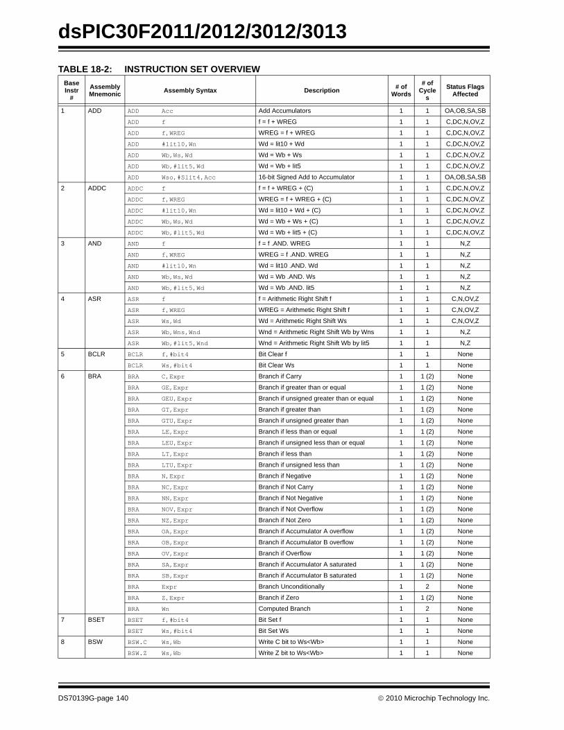
dsPIC30F2011/2012/3012/3013
TABLE 18-2: INSTRUCTION SET OVERVIEWBaseInstr
#AssemblyMnemonic Assembly Syntax Description # of
Words# of
Cycles
Status Flags Affected
1 ADD ADD Acc Add Accumulators 1 1 OA,OB,SA,SB
ADD f f = f + WREG 1 1 C,DC,N,OV,Z
ADD f,WREG WREG = f + WREG 1 1 C,DC,N,OV,Z
ADD #lit10,Wn Wd = lit10 + Wd 1 1 C,DC,N,OV,Z
ADD Wb,Ws,Wd Wd = Wb + Ws 1 1 C,DC,N,OV,Z
ADD Wb,#lit5,Wd Wd = Wb + lit5 1 1 C,DC,N,OV,Z
ADD Wso,#Slit4,Acc 16-bit Signed Add to Accumulator 1 1 OA,OB,SA,SB
2 ADDC ADDC f f = f + WREG + (C) 1 1 C,DC,N,OV,Z
ADDC f,WREG WREG = f + WREG + (C) 1 1 C,DC,N,OV,Z
ADDC #lit10,Wn Wd = lit10 + Wd + (C) 1 1 C,DC,N,OV,Z
ADDC Wb,Ws,Wd Wd = Wb + Ws + (C) 1 1 C,DC,N,OV,Z
ADDC Wb,#lit5,Wd Wd = Wb + lit5 + (C) 1 1 C,DC,N,OV,Z
3 AND AND f f = f .AND. WREG 1 1 N,Z
AND f,WREG WREG = f .AND. WREG 1 1 N,Z
AND #lit10,Wn Wd = lit10 .AND. Wd 1 1 N,Z
AND Wb,Ws,Wd Wd = Wb .AND. Ws 1 1 N,Z
AND Wb,#lit5,Wd Wd = Wb .AND. lit5 1 1 N,Z
4 ASR ASR f f = Arithmetic Right Shift f 1 1 C,N,OV,Z
ASR f,WREG WREG = Arithmetic Right Shift f 1 1 C,N,OV,Z
ASR Ws,Wd Wd = Arithmetic Right Shift Ws 1 1 C,N,OV,Z
ASR Wb,Wns,Wnd Wnd = Arithmetic Right Shift Wb by Wns 1 1 N,Z
ASR Wb,#lit5,Wnd Wnd = Arithmetic Right Shift Wb by lit5 1 1 N,Z
5 BCLR BCLR f,#bit4 Bit Clear f 1 1 None
BCLR Ws,#bit4 Bit Clear Ws 1 1 None
6 BRA BRA C,Expr Branch if Carry 1 1 (2) None
BRA GE,Expr Branch if greater than or equal 1 1 (2) None
BRA GEU,Expr Branch if unsigned greater than or equal 1 1 (2) None
BRA GT,Expr Branch if greater than 1 1 (2) None
BRA GTU,Expr Branch if unsigned greater than 1 1 (2) None
BRA LE,Expr Branch if less than or equal 1 1 (2) None
BRA LEU,Expr Branch if unsigned less than or equal 1 1 (2) None
BRA LT,Expr Branch if less than 1 1 (2) None
BRA LTU,Expr Branch if unsigned less than 1 1 (2) None
BRA N,Expr Branch if Negative 1 1 (2) None
BRA NC,Expr Branch if Not Carry 1 1 (2) None
BRA NN,Expr Branch if Not Negative 1 1 (2) None
BRA NOV,Expr Branch if Not Overflow 1 1 (2) None
BRA NZ,Expr Branch if Not Zero 1 1 (2) None
BRA OA,Expr Branch if Accumulator A overflow 1 1 (2) None
BRA OB,Expr Branch if Accumulator B overflow 1 1 (2) None
BRA OV,Expr Branch if Overflow 1 1 (2) None
BRA SA,Expr Branch if Accumulator A saturated 1 1 (2) None
BRA SB,Expr Branch if Accumulator B saturated 1 1 (2) None
BRA Expr Branch Unconditionally 1 2 None
BRA Z,Expr Branch if Zero 1 1 (2) None
BRA Wn Computed Branch 1 2 None
7 BSET BSET f,#bit4 Bit Set f 1 1 None
BSET Ws,#bit4 Bit Set Ws 1 1 None
8 BSW BSW.C Ws,Wb Write C bit to Ws<Wb> 1 1 None
BSW.Z Ws,Wb Write Z bit to Ws<Wb> 1 1 None
DS70139G-page 140 © 2010 Microchip Technology Inc.
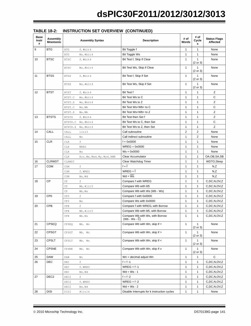
dsPIC30F2011/2012/3012/3013
9 BTG BTG f,#bit4 Bit Toggle f 1 1 None
BTG Ws,#bit4 Bit Toggle Ws 1 1 None
10 BTSC BTSC f,#bit4 Bit Test f, Skip if Clear 1 1 (2 or 3)
None
BTSC Ws,#bit4 Bit Test Ws, Skip if Clear 1 1 (2 or 3)
None
11 BTSS BTSS f,#bit4 Bit Test f, Skip if Set 1 1 (2 or 3)
None
BTSS Ws,#bit4 Bit Test Ws, Skip if Set 1 1 (2 or 3)
None
12 BTST BTST f,#bit4 Bit Test f 1 1 Z
BTST.C Ws,#bit4 Bit Test Ws to C 1 1 C
BTST.Z Ws,#bit4 Bit Test Ws to Z 1 1 Z
BTST.C Ws,Wb Bit Test Ws<Wb> to C 1 1 C
BTST.Z Ws,Wb Bit Test Ws<Wb> to Z 1 1 Z
13 BTSTS BTSTS f,#bit4 Bit Test then Set f 1 1 Z
BTSTS.C Ws,#bit4 Bit Test Ws to C, then Set 1 1 C
BTSTS.Z Ws,#bit4 Bit Test Ws to Z, then Set 1 1 Z
14 CALL CALL lit23 Call subroutine 2 2 None
CALL Wn Call indirect subroutine 1 2 None
15 CLR CLR f f = 0x0000 1 1 None
CLR WREG WREG = 0x0000 1 1 None
CLR Ws Ws = 0x0000 1 1 None
CLR Acc,Wx,Wxd,Wy,Wyd,AWB Clear Accumulator 1 1 OA,OB,SA,SB
16 CLRWDT CLRWDT Clear Watchdog Timer 1 1 WDTO,Sleep
17 COM COM f f = f 1 1 N,Z
COM f,WREG WREG = f 1 1 N,Z
COM Ws,Wd Wd = Ws 1 1 N,Z
18 CP CP f Compare f with WREG 1 1 C,DC,N,OV,Z
CP Wb,#lit5 Compare Wb with lit5 1 1 C,DC,N,OV,Z
CP Wb,Ws Compare Wb with Ws (Wb - Ws) 1 1 C,DC,N,OV,Z
19 CP0 CP0 f Compare f with 0x0000 1 1 C,DC,N,OV,Z
CP0 Ws Compare Ws with 0x0000 1 1 C,DC,N,OV,Z
20 CPB CPB f Compare f with WREG, with Borrow 1 1 C,DC,N,OV,Z
CPB Wb,#lit5 Compare Wb with lit5, with Borrow 1 1 C,DC,N,OV,Z
CPB Wb,Ws Compare Wb with Ws, with Borrow (Wb - Ws - C)
1 1 C,DC,N,OV,Z
21 CPSEQ CPSEQ Wb, Wn Compare Wb with Wn, skip if = 1 1 (2 or 3)
None
22 CPSGT CPSGT Wb, Wn Compare Wb with Wn, skip if > 1 1 (2 or 3)
None
23 CPSLT CPSLT Wb, Wn Compare Wb with Wn, skip if < 1 1 (2 or 3)
None
24 CPSNE CPSNE Wb, Wn Compare Wb with Wn, skip if ≠ 1 1 (2 or 3)
None
25 DAW DAW Wn Wn = decimal adjust Wn 1 1 C
26 DEC DEC f f = f -1 1 1 C,DC,N,OV,Z
DEC f,WREG WREG = f -1 1 1 C,DC,N,OV,Z
DEC Ws,Wd Wd = Ws - 1 1 1 C,DC,N,OV,Z
27 DEC2 DEC2 f f = f -2 1 1 C,DC,N,OV,Z
DEC2 f,WREG WREG = f -2 1 1 C,DC,N,OV,Z
DEC2 Ws,Wd Wd = Ws - 2 1 1 C,DC,N,OV,Z
28 DISI DISI #lit14 Disable Interrupts for k instruction cycles 1 1 None
TABLE 18-2: INSTRUCTION SET OVERVIEW (CONTINUED) BaseInstr
#AssemblyMnemonic Assembly Syntax Description # of
Words# of
Cycles
Status Flags Affected
© 2010 Microchip Technology Inc. DS70139G-page 141
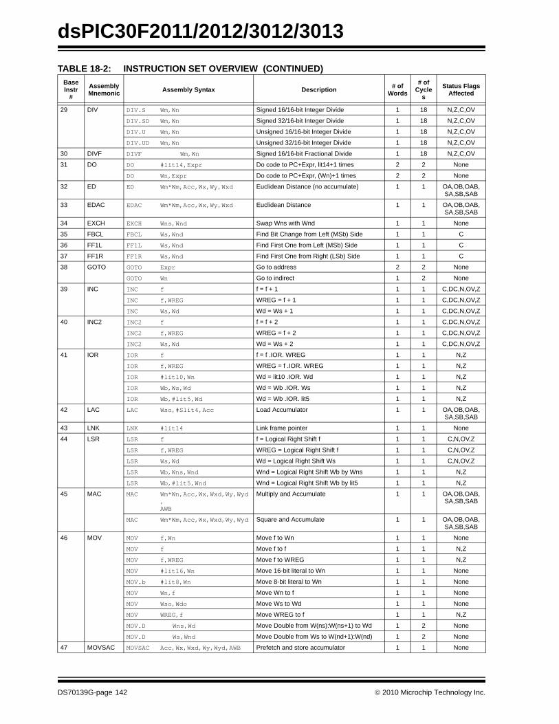
dsPIC30F2011/2012/3012/3013
29 DIV DIV.S Wm,Wn Signed 16/16-bit Integer Divide 1 18 N,Z,C,OV
DIV.SD Wm,Wn Signed 32/16-bit Integer Divide 1 18 N,Z,C,OV
DIV.U Wm,Wn Unsigned 16/16-bit Integer Divide 1 18 N,Z,C,OV
DIV.UD Wm,Wn Unsigned 32/16-bit Integer Divide 1 18 N,Z,C,OV
30 DIVF DIVF Wm,Wn Signed 16/16-bit Fractional Divide 1 18 N,Z,C,OV
31 DO DO #lit14,Expr Do code to PC+Expr, lit14+1 times 2 2 None
DO Wn,Expr Do code to PC+Expr, (Wn)+1 times 2 2 None
32 ED ED Wm*Wm,Acc,Wx,Wy,Wxd Euclidean Distance (no accumulate) 1 1 OA,OB,OAB,SA,SB,SAB
33 EDAC EDAC Wm*Wm,Acc,Wx,Wy,Wxd Euclidean Distance 1 1 OA,OB,OAB,SA,SB,SAB
34 EXCH EXCH Wns,Wnd Swap Wns with Wnd 1 1 None
35 FBCL FBCL Ws,Wnd Find Bit Change from Left (MSb) Side 1 1 C
36 FF1L FF1L Ws,Wnd Find First One from Left (MSb) Side 1 1 C
37 FF1R FF1R Ws,Wnd Find First One from Right (LSb) Side 1 1 C
38 GOTO GOTO Expr Go to address 2 2 None
GOTO Wn Go to indirect 1 2 None
39 INC INC f f = f + 1 1 1 C,DC,N,OV,Z
INC f,WREG WREG = f + 1 1 1 C,DC,N,OV,Z
INC Ws,Wd Wd = Ws + 1 1 1 C,DC,N,OV,Z
40 INC2 INC2 f f = f + 2 1 1 C,DC,N,OV,Z
INC2 f,WREG WREG = f + 2 1 1 C,DC,N,OV,Z
INC2 Ws,Wd Wd = Ws + 2 1 1 C,DC,N,OV,Z
41 IOR IOR f f = f .IOR. WREG 1 1 N,Z
IOR f,WREG WREG = f .IOR. WREG 1 1 N,Z
IOR #lit10,Wn Wd = lit10 .IOR. Wd 1 1 N,Z
IOR Wb,Ws,Wd Wd = Wb .IOR. Ws 1 1 N,Z
IOR Wb,#lit5,Wd Wd = Wb .IOR. lit5 1 1 N,Z
42 LAC LAC Wso,#Slit4,Acc Load Accumulator 1 1 OA,OB,OAB,SA,SB,SAB
43 LNK LNK #lit14 Link frame pointer 1 1 None
44 LSR LSR f f = Logical Right Shift f 1 1 C,N,OV,Z
LSR f,WREG WREG = Logical Right Shift f 1 1 C,N,OV,Z
LSR Ws,Wd Wd = Logical Right Shift Ws 1 1 C,N,OV,Z
LSR Wb,Wns,Wnd Wnd = Logical Right Shift Wb by Wns 1 1 N,Z
LSR Wb,#lit5,Wnd Wnd = Logical Right Shift Wb by lit5 1 1 N,Z
45 MAC MAC Wm*Wn,Acc,Wx,Wxd,Wy,Wyd,AWB
Multiply and Accumulate 1 1 OA,OB,OAB,SA,SB,SAB
MAC Wm*Wm,Acc,Wx,Wxd,Wy,Wyd Square and Accumulate 1 1 OA,OB,OAB,SA,SB,SAB
46 MOV MOV f,Wn Move f to Wn 1 1 None
MOV f Move f to f 1 1 N,Z
MOV f,WREG Move f to WREG 1 1 N,Z
MOV #lit16,Wn Move 16-bit literal to Wn 1 1 None
MOV.b #lit8,Wn Move 8-bit literal to Wn 1 1 None
MOV Wn,f Move Wn to f 1 1 None
MOV Wso,Wdo Move Ws to Wd 1 1 None
MOV WREG,f Move WREG to f 1 1 N,Z
MOV.D Wns,Wd Move Double from W(ns):W(ns+1) to Wd 1 2 None
MOV.D Ws,Wnd Move Double from Ws to W(nd+1):W(nd) 1 2 None
47 MOVSAC MOVSAC Acc,Wx,Wxd,Wy,Wyd,AWB Prefetch and store accumulator 1 1 None
TABLE 18-2: INSTRUCTION SET OVERVIEW (CONTINUED) BaseInstr
#AssemblyMnemonic Assembly Syntax Description # of
Words# of
Cycles
Status Flags Affected
DS70139G-page 142 © 2010 Microchip Technology Inc.
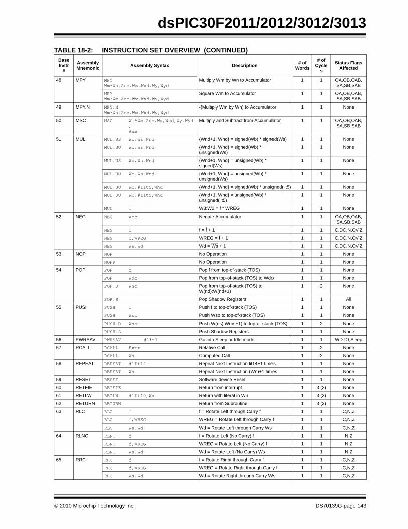
dsPIC30F2011/2012/3012/3013
48 MPY MPY Wm*Wn,Acc,Wx,Wxd,Wy,Wyd
Multiply Wm by Wn to Accumulator 1 1 OA,OB,OAB,SA,SB,SAB
MPY Wm*Wm,Acc,Wx,Wxd,Wy,Wyd
Square Wm to Accumulator 1 1 OA,OB,OAB,SA,SB,SAB
49 MPY.N MPY.N Wm*Wn,Acc,Wx,Wxd,Wy,Wyd
-(Multiply Wm by Wn) to Accumulator 1 1 None
50 MSC MSC Wm*Wm,Acc,Wx,Wxd,Wy,Wyd,AWB
Multiply and Subtract from Accumulator 1 1 OA,OB,OAB,SA,SB,SAB
51 MUL MUL.SS Wb,Ws,Wnd {Wnd+1, Wnd} = signed(Wb) * signed(Ws) 1 1 None
MUL.SU Wb,Ws,Wnd {Wnd+1, Wnd} = signed(Wb) * unsigned(Ws)
1 1 None
MUL.US Wb,Ws,Wnd {Wnd+1, Wnd} = unsigned(Wb) * signed(Ws)
1 1 None
MUL.UU Wb,Ws,Wnd {Wnd+1, Wnd} = unsigned(Wb) * unsigned(Ws)
1 1 None
MUL.SU Wb,#lit5,Wnd {Wnd+1, Wnd} = signed(Wb) * unsigned(lit5) 1 1 None
MUL.UU Wb,#lit5,Wnd {Wnd+1, Wnd} = unsigned(Wb) * unsigned(lit5)
1 1 None
MUL f W3:W2 = f * WREG 1 1 None
52 NEG NEG Acc Negate Accumulator 1 1 OA,OB,OAB,SA,SB,SAB
NEG f f = f + 1 1 1 C,DC,N,OV,Z
NEG f,WREG WREG = f + 1 1 1 C,DC,N,OV,Z
NEG Ws,Wd Wd = Ws + 1 1 1 C,DC,N,OV,Z
53 NOP NOP No Operation 1 1 None
NOPR No Operation 1 1 None
54 POP POP f Pop f from top-of-stack (TOS) 1 1 None
POP Wdo Pop from top-of-stack (TOS) to Wdo 1 1 None
POP.D Wnd Pop from top-of-stack (TOS) to W(nd):W(nd+1)
1 2 None
POP.S Pop Shadow Registers 1 1 All
55 PUSH PUSH f Push f to top-of-stack (TOS) 1 1 None
PUSH Wso Push Wso to top-of-stack (TOS) 1 1 None
PUSH.D Wns Push W(ns):W(ns+1) to top-of-stack (TOS) 1 2 None
PUSH.S Push Shadow Registers 1 1 None
56 PWRSAV PWRSAV #lit1 Go into Sleep or Idle mode 1 1 WDTO,Sleep
57 RCALL RCALL Expr Relative Call 1 2 None
RCALL Wn Computed Call 1 2 None
58 REPEAT REPEAT #lit14 Repeat Next Instruction lit14+1 times 1 1 None
REPEAT Wn Repeat Next Instruction (Wn)+1 times 1 1 None
59 RESET RESET Software device Reset 1 1 None
60 RETFIE RETFIE Return from interrupt 1 3 (2) None
61 RETLW RETLW #lit10,Wn Return with literal in Wn 1 3 (2) None
62 RETURN RETURN Return from Subroutine 1 3 (2) None
63 RLC RLC f f = Rotate Left through Carry f 1 1 C,N,Z
RLC f,WREG WREG = Rotate Left through Carry f 1 1 C,N,Z
RLC Ws,Wd Wd = Rotate Left through Carry Ws 1 1 C,N,Z
64 RLNC RLNC f f = Rotate Left (No Carry) f 1 1 N,Z
RLNC f,WREG WREG = Rotate Left (No Carry) f 1 1 N,Z
RLNC Ws,Wd Wd = Rotate Left (No Carry) Ws 1 1 N,Z
65 RRC RRC f f = Rotate Right through Carry f 1 1 C,N,Z
RRC f,WREG WREG = Rotate Right through Carry f 1 1 C,N,Z
RRC Ws,Wd Wd = Rotate Right through Carry Ws 1 1 C,N,Z
TABLE 18-2: INSTRUCTION SET OVERVIEW (CONTINUED) BaseInstr
#AssemblyMnemonic Assembly Syntax Description # of
Words# of
Cycles
Status Flags Affected
© 2010 Microchip Technology Inc. DS70139G-page 143
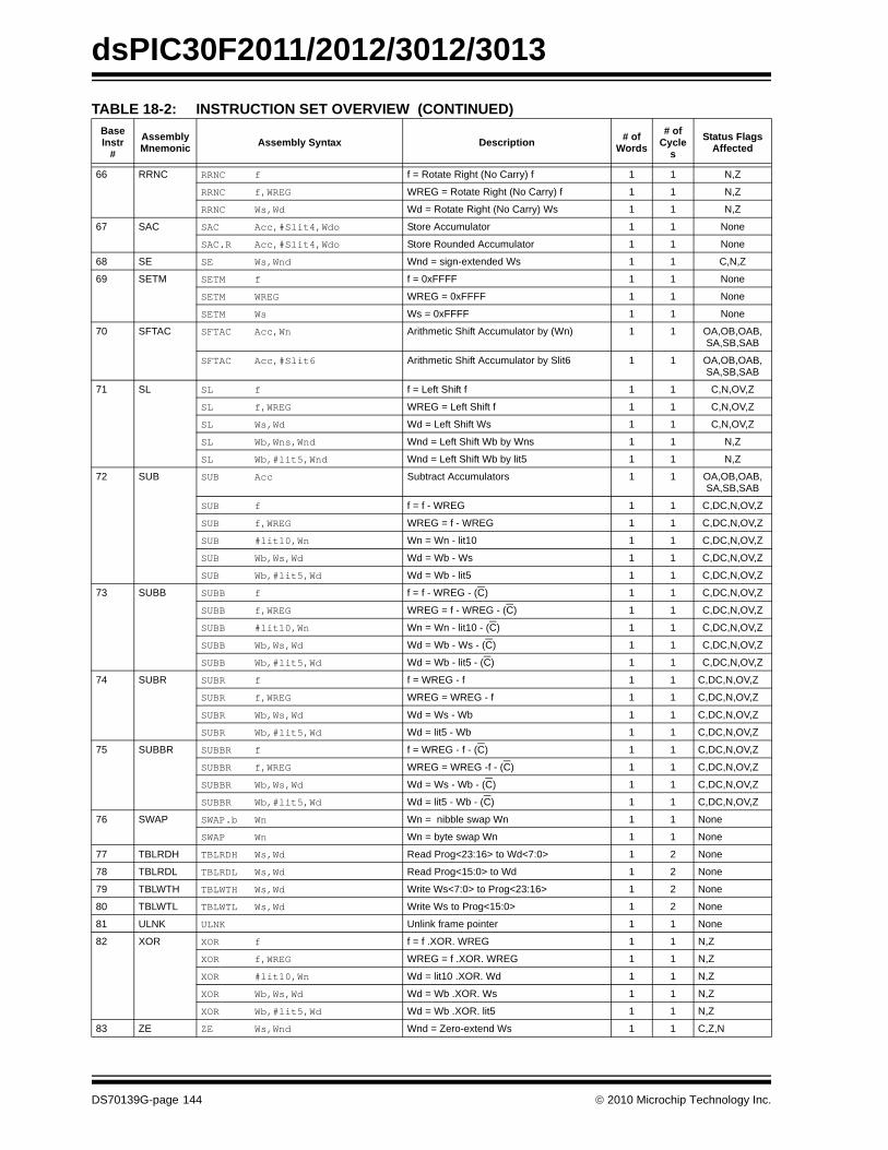
dsPIC30F2011/2012/3012/3013
66 RRNC RRNC f f = Rotate Right (No Carry) f 1 1 N,Z
RRNC f,WREG WREG = Rotate Right (No Carry) f 1 1 N,Z
RRNC Ws,Wd Wd = Rotate Right (No Carry) Ws 1 1 N,Z
67 SAC SAC Acc,#Slit4,Wdo Store Accumulator 1 1 None
SAC.R Acc,#Slit4,Wdo Store Rounded Accumulator 1 1 None
68 SE SE Ws,Wnd Wnd = sign-extended Ws 1 1 C,N,Z
69 SETM SETM f f = 0xFFFF 1 1 None
SETM WREG WREG = 0xFFFF 1 1 None
SETM Ws Ws = 0xFFFF 1 1 None
70 SFTAC SFTAC Acc,Wn Arithmetic Shift Accumulator by (Wn) 1 1 OA,OB,OAB,SA,SB,SAB
SFTAC Acc,#Slit6 Arithmetic Shift Accumulator by Slit6 1 1 OA,OB,OAB,SA,SB,SAB
71 SL SL f f = Left Shift f 1 1 C,N,OV,Z
SL f,WREG WREG = Left Shift f 1 1 C,N,OV,Z
SL Ws,Wd Wd = Left Shift Ws 1 1 C,N,OV,Z
SL Wb,Wns,Wnd Wnd = Left Shift Wb by Wns 1 1 N,Z
SL Wb,#lit5,Wnd Wnd = Left Shift Wb by lit5 1 1 N,Z
72 SUB SUB Acc Subtract Accumulators 1 1 OA,OB,OAB,SA,SB,SAB
SUB f f = f - WREG 1 1 C,DC,N,OV,Z
SUB f,WREG WREG = f - WREG 1 1 C,DC,N,OV,Z
SUB #lit10,Wn Wn = Wn - lit10 1 1 C,DC,N,OV,Z
SUB Wb,Ws,Wd Wd = Wb - Ws 1 1 C,DC,N,OV,Z
SUB Wb,#lit5,Wd Wd = Wb - lit5 1 1 C,DC,N,OV,Z
73 SUBB SUBB f f = f - WREG - (C) 1 1 C,DC,N,OV,Z
SUBB f,WREG WREG = f - WREG - (C) 1 1 C,DC,N,OV,Z
SUBB #lit10,Wn Wn = Wn - lit10 - (C) 1 1 C,DC,N,OV,Z
SUBB Wb,Ws,Wd Wd = Wb - Ws - (C) 1 1 C,DC,N,OV,Z
SUBB Wb,#lit5,Wd Wd = Wb - lit5 - (C) 1 1 C,DC,N,OV,Z
74 SUBR SUBR f f = WREG - f 1 1 C,DC,N,OV,Z
SUBR f,WREG WREG = WREG - f 1 1 C,DC,N,OV,Z
SUBR Wb,Ws,Wd Wd = Ws - Wb 1 1 C,DC,N,OV,Z
SUBR Wb,#lit5,Wd Wd = lit5 - Wb 1 1 C,DC,N,OV,Z
75 SUBBR SUBBR f f = WREG - f - (C) 1 1 C,DC,N,OV,Z
SUBBR f,WREG WREG = WREG -f - (C) 1 1 C,DC,N,OV,Z
SUBBR Wb,Ws,Wd Wd = Ws - Wb - (C) 1 1 C,DC,N,OV,Z
SUBBR Wb,#lit5,Wd Wd = lit5 - Wb - (C) 1 1 C,DC,N,OV,Z
76 SWAP SWAP.b Wn Wn = nibble swap Wn 1 1 None
SWAP Wn Wn = byte swap Wn 1 1 None
77 TBLRDH TBLRDH Ws,Wd Read Prog<23:16> to Wd<7:0> 1 2 None
78 TBLRDL TBLRDL Ws,Wd Read Prog<15:0> to Wd 1 2 None
79 TBLWTH TBLWTH Ws,Wd Write Ws<7:0> to Prog<23:16> 1 2 None
80 TBLWTL TBLWTL Ws,Wd Write Ws to Prog<15:0> 1 2 None
81 ULNK ULNK Unlink frame pointer 1 1 None
82 XOR XOR f f = f .XOR. WREG 1 1 N,Z
XOR f,WREG WREG = f .XOR. WREG 1 1 N,Z
XOR #lit10,Wn Wd = lit10 .XOR. Wd 1 1 N,Z
XOR Wb,Ws,Wd Wd = Wb .XOR. Ws 1 1 N,Z
XOR Wb,#lit5,Wd Wd = Wb .XOR. lit5 1 1 N,Z
83 ZE ZE Ws,Wnd Wnd = Zero-extend Ws 1 1 C,Z,N
TABLE 18-2: INSTRUCTION SET OVERVIEW (CONTINUED) BaseInstr
#AssemblyMnemonic Assembly Syntax Description # of
Words# of
Cycles
Status Flags Affected
DS70139G-page 144 © 2010 Microchip Technology Inc.
dsPIC30F2011/2012/3012/3013
19.0 DEVELOPMENT SUPPORTThe PIC® microcontrollers and dsPIC® digital signalcontrollers are supported with a full range of softwareand hardware development tools:
• Integrated Development Environment- MPLAB® IDE Software
• Compilers/Assemblers/Linkers- MPLAB C Compiler for Various Device
Families- HI-TECH C for Various Device Families- MPASMTM Assembler- MPLINKTM Object Linker/
MPLIBTM Object Librarian- MPLAB Assembler/Linker/Librarian for
Various Device Families• Simulators
- MPLAB SIM Software Simulator• Emulators
- MPLAB REAL ICE™ In-Circuit Emulator• In-Circuit Debuggers
- MPLAB ICD 3- PICkit™ 3 Debug Express
• Device Programmers- PICkit™ 2 Programmer- MPLAB PM3 Device Programmer
• Low-Cost Demonstration/Development Boards, Evaluation Kits, and Starter Kits
19.1 MPLAB Integrated Development Environment Software
The MPLAB IDE software brings an ease of softwaredevelopment previously unseen in the 8/16/32-bitmicrocontroller market. The MPLAB IDE is a Windows®
operating system-based application that contains:
• A single graphical interface to all debugging tools- Simulator- Programmer (sold separately)- In-Circuit Emulator (sold separately)- In-Circuit Debugger (sold separately)
• A full-featured editor with color-coded context• A multiple project manager• Customizable data windows with direct edit of
contents• High-level source code debugging• Mouse over variable inspection• Drag and drop variables from source to watch
windows• Extensive on-line help• Integration of select third party tools, such as
IAR C Compilers
The MPLAB IDE allows you to:
• Edit your source files (either C or assembly)• One-touch compile or assemble, and download to
emulator and simulator tools (automatically updates all project information)
• Debug using:- Source files (C or assembly)- Mixed C and assembly- Machine code
MPLAB IDE supports multiple debugging tools in asingle development paradigm, from the cost-effectivesimulators, through low-cost in-circuit debuggers, tofull-featured emulators. This eliminates the learningcurve when upgrading to tools with increased flexibilityand power.
© 2010 Microchip Technology Inc. DS70139G-page 145
dsPIC30F2011/2012/3012/3013
19.2 MPLAB C Compilers for VariousDevice FamiliesThe MPLAB C Compiler code development systemsare complete ANSI C compilers for Microchip’s PIC18,PIC24 and PIC32 families of microcontrollers and thedsPIC30 and dsPIC33 families of digital signal control-lers. These compilers provide powerful integrationcapabilities, superior code optimization and ease ofuse.
For easy source level debugging, the compilers providesymbol information that is optimized to the MPLAB IDEdebugger.
19.3 HI-TECH C for Various Device Families
The HI-TECH C Compiler code development systemsare complete ANSI C compilers for Microchip’s PICfamily of microcontrollers and the dsPIC family of digitalsignal controllers. These compilers provide powerfulintegration capabilities, omniscient code generationand ease of use.
For easy source level debugging, the compilers providesymbol information that is optimized to the MPLAB IDEdebugger.
The compilers include a macro assembler, linker, pre-processor, and one-step driver, and can run on multipleplatforms.
19.4 MPASM AssemblerThe MPASM Assembler is a full-featured, universalmacro assembler for PIC10/12/16/18 MCUs.
The MPASM Assembler generates relocatable objectfiles for the MPLINK Object Linker, Intel® standard HEXfiles, MAP files to detail memory usage and symbolreference, absolute LST files that contain source linesand generated machine code and COFF files fordebugging.
The MPASM Assembler features include:
• Integration into MPLAB IDE projects• User-defined macros to streamline
assembly code• Conditional assembly for multi-purpose
source files• Directives that allow complete control over the
assembly process
19.5 MPLINK Object Linker/MPLIB Object Librarian
The MPLINK Object Linker combines relocatableobjects created by the MPASM Assembler and theMPLAB C18 C Compiler. It can link relocatable objectsfrom precompiled libraries, using directives from alinker script.
The MPLIB Object Librarian manages the creation andmodification of library files of precompiled code. Whena routine from a library is called from a source file, onlythe modules that contain that routine will be linked inwith the application. This allows large libraries to beused efficiently in many different applications.
The object linker/library features include:
• Efficient linking of single libraries instead of many smaller files
• Enhanced code maintainability by grouping related modules together
• Flexible creation of libraries with easy module listing, replacement, deletion and extraction
19.6 MPLAB Assembler, Linker and Librarian for Various Device Families
MPLAB Assembler produces relocatable machinecode from symbolic assembly language for PIC24,PIC32 and dsPIC devices. MPLAB C Compiler usesthe assembler to produce its object file. The assemblergenerates relocatable object files that can then bearchived or linked with other relocatable object files andarchives to create an executable file. Notable featuresof the assembler include:
• Support for the entire device instruction set• Support for fixed-point and floating-point data• Command line interface• Rich directive set• Flexible macro language• MPLAB IDE compatibility
DS70139G-page 146 © 2010 Microchip Technology Inc.
dsPIC30F2011/2012/3012/3013
19.7 MPLAB SIM Software SimulatorThe MPLAB SIM Software Simulator allows codedevelopment in a PC-hosted environment by simulat-ing the PIC MCUs and dsPIC® DSCs on an instructionlevel. On any given instruction, the data areas can beexamined or modified and stimuli can be applied froma comprehensive stimulus controller. Registers can belogged to files for further run-time analysis. The tracebuffer and logic analyzer display extend the power ofthe simulator to record and track program execution,actions on I/O, most peripherals and internal registers.The MPLAB SIM Software Simulator fully supportssymbolic debugging using the MPLAB C Compilers,and the MPASM and MPLAB Assemblers. The soft-ware simulator offers the flexibility to develop anddebug code outside of the hardware laboratory envi-ronment, making it an excellent, economical softwaredevelopment tool.
19.8 MPLAB REAL ICE In-Circuit Emulator System
MPLAB REAL ICE In-Circuit Emulator System isMicrochip’s next generation high-speed emulator forMicrochip Flash DSC and MCU devices. It debugs andprograms PIC® Flash MCUs and dsPIC® Flash DSCswith the easy-to-use, powerful graphical user interface ofthe MPLAB Integrated Development Environment (IDE),included with each kit.
The emulator is connected to the design engineer’s PCusing a high-speed USB 2.0 interface and is connectedto the target with either a connector compatible with in-circuit debugger systems (RJ11) or with the new high-speed, noise tolerant, Low-Voltage Differential Signal(LVDS) interconnection (CAT5).
The emulator is field upgradable through future firmwaredownloads in MPLAB IDE. In upcoming releases ofMPLAB IDE, new devices will be supported, and newfeatures will be added. MPLAB REAL ICE offerssignificant advantages over competitive emulatorsincluding low-cost, full-speed emulation, run-timevariable watches, trace analysis, complex breakpoints, aruggedized probe interface and long (up to three meters)interconnection cables.
19.9 MPLAB ICD 3 In-Circuit Debugger System
MPLAB ICD 3 In-Circuit Debugger System is Micro-chip's most cost effective high-speed hardwaredebugger/programmer for Microchip Flash Digital Sig-nal Controller (DSC) and microcontroller (MCU)devices. It debugs and programs PIC® Flash microcon-trollers and dsPIC® DSCs with the powerful, yet easy-to-use graphical user interface of MPLAB IntegratedDevelopment Environment (IDE).
The MPLAB ICD 3 In-Circuit Debugger probe is con-nected to the design engineer's PC using a high-speedUSB 2.0 interface and is connected to the target with aconnector compatible with the MPLAB ICD 2 or MPLABREAL ICE systems (RJ-11). MPLAB ICD 3 supports allMPLAB ICD 2 headers.
19.10 PICkit 3 In-Circuit Debugger/Programmer and PICkit 3 Debug Express
The MPLAB PICkit 3 allows debugging and program-ming of PIC® and dsPIC® Flash microcontrollers at amost affordable price point using the powerful graphicaluser interface of the MPLAB Integrated DevelopmentEnvironment (IDE). The MPLAB PICkit 3 is connectedto the design engineer's PC using a full speed USBinterface and can be connected to the target via anMicrochip debug (RJ-11) connector (compatible withMPLAB ICD 3 and MPLAB REAL ICE). The connectoruses two device I/O pins and the reset line to imple-ment in-circuit debugging and In-Circuit Serial Pro-gramming™.
The PICkit 3 Debug Express include the PICkit 3, demoboard and microcontroller, hookup cables and CDROMwith user’s guide, lessons, tutorial, compiler andMPLAB IDE software.
© 2010 Microchip Technology Inc. DS70139G-page 147
dsPIC30F2011/2012/3012/3013
19.11 PICkit 2 DevelopmentProgrammer/Debugger and PICkit 2 Debug Express
The PICkit™ 2 Development Programmer/Debugger isa low-cost development tool with an easy to use inter-face for programming and debugging Microchip’s Flashfamilies of microcontrollers. The full featuredWindows® programming interface supports baseline(PIC10F, PIC12F5xx, PIC16F5xx), midrange(PIC12F6xx, PIC16F), PIC18F, PIC24, dsPIC30,dsPIC33, and PIC32 families of 8-bit, 16-bit, and 32-bitmicrocontrollers, and many Microchip Serial EEPROMproducts. With Microchip’s powerful MPLAB IntegratedDevelopment Environment (IDE) the PICkit™ 2enables in-circuit debugging on most PIC® microcon-trollers. In-Circuit-Debugging runs, halts and singlesteps the program while the PIC microcontroller isembedded in the application. When halted at a break-point, the file registers can be examined and modified.
The PICkit 2 Debug Express include the PICkit 2, demoboard and microcontroller, hookup cables and CDROMwith user’s guide, lessons, tutorial, compiler andMPLAB IDE software.
19.12 MPLAB PM3 Device ProgrammerThe MPLAB PM3 Device Programmer is a universal,CE compliant device programmer with programmablevoltage verification at VDDMIN and VDDMAX formaximum reliability. It features a large LCD display(128 x 64) for menus and error messages and a modu-lar, detachable socket assembly to support variouspackage types. The ICSP™ cable assembly is includedas a standard item. In Stand-Alone mode, the MPLABPM3 Device Programmer can read, verify and programPIC devices without a PC connection. It can also setcode protection in this mode. The MPLAB PM3connects to the host PC via an RS-232 or USB cable.The MPLAB PM3 has high-speed communications andoptimized algorithms for quick programming of largememory devices and incorporates an MMC card for filestorage and data applications.
19.13 Demonstration/Development Boards, Evaluation Kits, and Starter Kits
A wide variety of demonstration, development andevaluation boards for various PIC MCUs and dsPICDSCs allows quick application development on fully func-tional systems. Most boards include prototyping areas foradding custom circuitry and provide application firmwareand source code for examination and modification.
The boards support a variety of features, including LEDs,temperature sensors, switches, speakers, RS-232interfaces, LCD displays, potentiometers and additionalEEPROM memory.
The demonstration and development boards can beused in teaching environments, for prototyping customcircuits and for learning about various microcontrollerapplications.
In addition to the PICDEM™ and dsPICDEM™ demon-stration/development board series of circuits, Microchiphas a line of evaluation kits and demonstration softwarefor analog filter design, KEELOQ® security ICs, CAN,IrDA®, PowerSmart battery management, SEEVAL®
evaluation system, Sigma-Delta ADC, flow ratesensing, plus many more.
Also available are starter kits that contain everythingneeded to experience the specified device. This usuallyincludes a single application and debug capability, allon one board.
Check the Microchip web page (www.microchip.com)for the complete list of demonstration, developmentand evaluation kits.
DS70139G-page 148 © 2010 Microchip Technology Inc.

dsPIC30F2011/2012/3012/3013
20.0 ELECTRICAL CHARACTERISTICSThis section provides an overview of dsPIC30F electrical characteristics. Additional information will be provided in futurerevisions of this document as it becomes available.
For detailed information about the dsPIC30F architecture and core, refer to the “dsPIC30F Family Reference Manual”(DS70046).
Absolute maximum ratings for the dsPIC30F family are listed below. Exposure to these maximum rating conditions forextended periods may affect device reliability. Functional operation of the device at these or any other conditions abovethe parameters indicated in the operation listings of this specification is not implied.
Absolute Maximum Ratings(†) Ambient temperature under bias............................................................................................................ .-40°C to +125°CStorage temperature .............................................................................................................................. -65°C to +150°CVoltage on any pin with respect to VSS (except VDD and MCLR) (Note 1) ..................................... -0.3V to (VDD + 0.3V)Voltage on VDD with respect to VSS ......................................................................................................... -0.3V to +5.5VVoltage on MCLR with respect to VSS........................................................................................................ 0V to +13.25VMaximum current out of VSS pin ...........................................................................................................................300 mAMaximum current into VDD pin (Note 2)................................................................................................................250 mAInput clamp current, IIK (VI < 0 or VI > VDD) ..........................................................................................................±20 mAOutput clamp current, IOK (VO < 0 or VO > VDD) ...................................................................................................±20 mAMaximum output current sunk by any I/O pin..........................................................................................................25 mAMaximum output current sourced by any I/O pin ....................................................................................................25 mAMaximum current sunk by all ports .......................................................................................................................200 mAMaximum current sourced by all ports (Note 2)....................................................................................................200 mA
Note 1: Voltage spikes below VSS at the MCLR/VPP pin, inducing currents greater than 80 mA, may cause latch-up.Thus, a series resistor of 50-100Ω should be used when applying a “low” level to the MCLR/VPP pin, ratherthan pulling this pin directly to VSS.
2: Maximum allowable current is a function of device maximum power dissipation. See Table 20-2 for PDMAX.
†NOTICE: Stresses above those listed under “Absolute Maximum Ratings” may cause permanent damage to thedevice. This is a stress rating only and functional operation of the device at those or any other conditions above thoseindicated in the operation listings of this specification is not implied. Exposure to maximum rating conditions forextended periods may affect device reliability.
Note: All peripheral electrical characteristics are specified. For exact peripherals available on specific devices, please refer to the dsPIC30F2011/2012/3012/3013 Sensor Family table on page 4 of this data sheet.
© 2010 Microchip Technology Inc. DS70139G-page 149
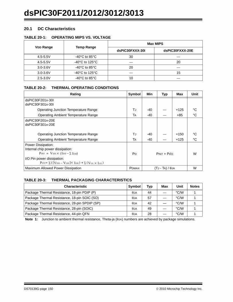
dsPIC30F2011/2012/3012/3013
20.1 DC CharacteristicsTABLE 20-1: OPERATING MIPS VS. VOLTAGE
VDD Range Temp RangeMax MIPS
dsPIC30FXXX-30I dsPIC30FXXX-20E
4.5-5.5V -40°C to 85°C 30 —4.5-5.5V -40°C to 125°C — 203.0-3.6V -40°C to 85°C 20 —3.0-3.6V -40°C to 125°C — 152.5-3.0V -40°C to 85°C 10 —
TABLE 20-2: THERMAL OPERATING CONDITIONSRating Symbol Min Typ Max Unit
dsPIC30F201x-30IdsPIC30F301x-30I
Operating Junction Temperature Range TJ -40 — +125 °COperating Ambient Temperature Range TA -40 — +85 °C
dsPIC30F201x-20EdsPIC30F301x-20E
Operating Junction Temperature Range TJ -40 — +150 °COperating Ambient Temperature Range TA -40 — +125 °C
Power Dissipation:Internal chip power dissipation:
PD PINT + PI/O WI/O Pin power dissipation:
Maximum Allowed Power Dissipation PDMAX (TJ - TA) / θJA W
PINT VDD IDD IOH∑–( )×=
PI/O VDD VOH–{ } IOH×( )∑ VOL I OL×( )∑+=
TABLE 20-3: THERMAL PACKAGING CHARACTERISTICSCharacteristic Symbol Typ Max Unit Notes
Package Thermal Resistance, 18-pin PDIP (P) θJA 44 — °C/W 1Package Thermal Resistance, 18-pin SOIC (SO) θJA 57 — °C/W 1Package Thermal Resistance, 28-pin SPDIP (SP) θJA 42 — °C/W 1Package Thermal Resistance, 28-pin (SOIC) θJA 49 — °C/W 1Package Thermal Resistance, 44-pin QFN θJA 28 — °C/W 1Note 1: Junction to ambient thermal resistance, Theta-ja (θJA) numbers are achieved by package simulations.
DS70139G-page 150 © 2010 Microchip Technology Inc.
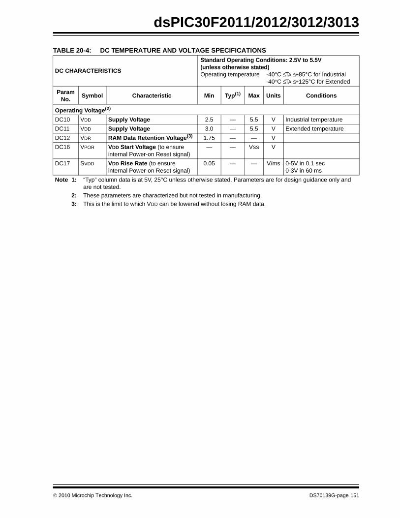
dsPIC30F2011/2012/3012/3013
TABLE 20-4: DC TEMPERATURE AND VOLTAGE SPECIFICATIONS
DC CHARACTERISTICS
Standard Operating Conditions: 2.5V to 5.5V(unless otherwise stated)Operating temperature -40°C ≤ TA ≤ +85°C for Industrial
-40°C ≤ TA ≤ +125°C for Extended
Param No. Symbol Characteristic Min Typ(1) Max Units Conditions
Operating Voltage(2)
DC10 VDD Supply Voltage 2.5 — 5.5 V Industrial temperatureDC11 VDD Supply Voltage 3.0 — 5.5 V Extended temperatureDC12 VDR RAM Data Retention Voltage(3) 1.75 — — VDC16 VPOR VDD Start Voltage (to ensure
internal Power-on Reset signal)— — VSS V
DC17 SVDD VDD Rise Rate (to ensure internal Power-on Reset signal)
0.05 — — V/ms 0-5V in 0.1 sec0-3V in 60 ms
Note 1: “Typ” column data is at 5V, 25°C unless otherwise stated. Parameters are for design guidance only and are not tested.
2: These parameters are characterized but not tested in manufacturing.3: This is the limit to which VDD can be lowered without losing RAM data.
© 2010 Microchip Technology Inc. DS70139G-page 151
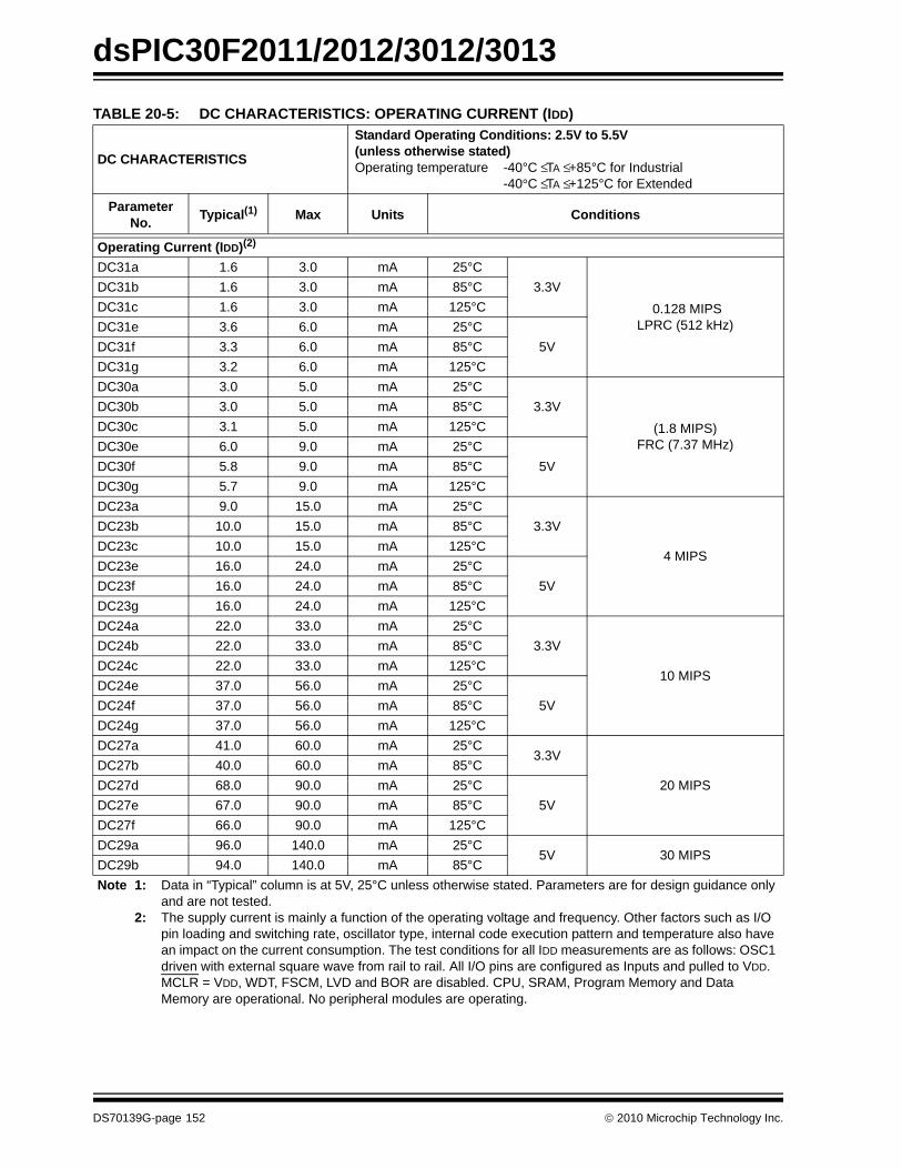
dsPIC30F2011/2012/3012/3013
TABLE 20-5: DC CHARACTERISTICS: OPERATING CURRENT (IDD)
DC CHARACTERISTICS
Standard Operating Conditions: 2.5V to 5.5V(unless otherwise stated)Operating temperature -40°C ≤ TA ≤ +85°C for Industrial
-40°C ≤ TA ≤ +125°C for Extended
Parameter No. Typical(1) Max Units Conditions
Operating Current (IDD)(2)
DC31a 1.6 3.0 mA 25°C3.3V
0.128 MIPSLPRC (512 kHz)
DC31b 1.6 3.0 mA 85°CDC31c 1.6 3.0 mA 125°CDC31e 3.6 6.0 mA 25°C
5VDC31f 3.3 6.0 mA 85°CDC31g 3.2 6.0 mA 125°CDC30a 3.0 5.0 mA 25°C
3.3V(1.8 MIPS)
FRC (7.37 MHz)
DC30b 3.0 5.0 mA 85°CDC30c 3.1 5.0 mA 125°CDC30e 6.0 9.0 mA 25°C
5VDC30f 5.8 9.0 mA 85°CDC30g 5.7 9.0 mA 125°CDC23a 9.0 15.0 mA 25°C
3.3V
4 MIPS
DC23b 10.0 15.0 mA 85°CDC23c 10.0 15.0 mA 125°CDC23e 16.0 24.0 mA 25°C
5VDC23f 16.0 24.0 mA 85°CDC23g 16.0 24.0 mA 125°CDC24a 22.0 33.0 mA 25°C
3.3V
10 MIPS
DC24b 22.0 33.0 mA 85°CDC24c 22.0 33.0 mA 125°CDC24e 37.0 56.0 mA 25°C
5VDC24f 37.0 56.0 mA 85°CDC24g 37.0 56.0 mA 125°CDC27a 41.0 60.0 mA 25°C
3.3V
20 MIPSDC27b 40.0 60.0 mA 85°CDC27d 68.0 90.0 mA 25°C
5VDC27e 67.0 90.0 mA 85°CDC27f 66.0 90.0 mA 125°CDC29a 96.0 140.0 mA 25°C
5V 30 MIPSDC29b 94.0 140.0 mA 85°CNote 1: Data in “Typical” column is at 5V, 25°C unless otherwise stated. Parameters are for design guidance only
and are not tested.2: The supply current is mainly a function of the operating voltage and frequency. Other factors such as I/O
pin loading and switching rate, oscillator type, internal code execution pattern and temperature also have an impact on the current consumption. The test conditions for all IDD measurements are as follows: OSC1 driven with external square wave from rail to rail. All I/O pins are configured as Inputs and pulled to VDD. MCLR = VDD, WDT, FSCM, LVD and BOR are disabled. CPU, SRAM, Program Memory and Data Memory are operational. No peripheral modules are operating.
DS70139G-page 152 © 2010 Microchip Technology Inc.
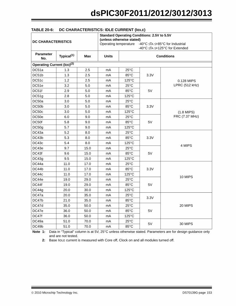
dsPIC30F2011/2012/3012/3013
TABLE 20-6: DC CHARACTERISTICS: IDLE CURRENT (IIDLE)
DC CHARACTERISTICS
Standard Operating Conditions: 2.5V to 5.5V(unless otherwise stated)Operating temperature -40°C ≤ TA ≤ +85°C for Industrial
-40°C ≤ TA ≤ +125°C for Extended
Parameter No. Typical(1) Max Units Conditions
Operating Current (IDD)(2)
DC51a 1.3 2.5 mA 25°C3.3V
0.128 MIPSLPRC (512 kHz)
DC51b 1.3 2.5 mA 85°CDC51c 1.2 2.5 mA 125°CDC51e 3.2 5.0 mA 25°C
5VDC51f 2.9 5.0 mA 85°CDC51g 2.8 5.0 mA 125°CDC50a 3.0 5.0 mA 25°C
3.3V(1.8 MIPS)
FRC (7.37 MHz)
DC50b 3.0 5.0 mA 85°CDC50c 3.0 5.0 mA 125°CDC50e 6.0 9.0 mA 25°C
5VDC50f 5.8 9.0 mA 85°CDC50g 5.7 9.0 mA 125°CDC43a 5.2 8.0 mA 25°C
3.3V
4 MIPS
DC43b 5.3 8.0 mA 85°CDC43c 5.4 8.0 mA 125°CDC43e 9.7 15.0 mA 25°C
5VDC43f 9.6 15.0 mA 85°CDC43g 9.5 15.0 mA 125°CDC44a 11.0 17.0 mA 25°C
3.3V
10 MIPS
DC44b 11.0 17.0 mA 85°CDC44c 11.0 17.0 mA 125°CDC44e 19.0 29.0 mA 25°C
5VDC44f 19.0 29.0 mA 85°CDC44g 20.0 30.0 mA 125°CDC47a 20.0 35.0 mA 25°C
3.3V
20 MIPSDC47b 21.0 35.0 mA 85°CDC47d 35.0 50.0 mA 25°C
5VDC47e 36.0 50.0 mA 85°CDC47f 36.0 50.0 mA 125°CDC49a 51.0 70.0 mA 25°C
5V 30 MIPSDC49b 51.0 70.0 mA 85°CNote 1: Data in “Typical” column is at 5V, 25°C unless otherwise stated. Parameters are for design guidance only
and are not tested.2: Base IIDLE current is measured with Core off, Clock on and all modules turned off.
© 2010 Microchip Technology Inc. DS70139G-page 153
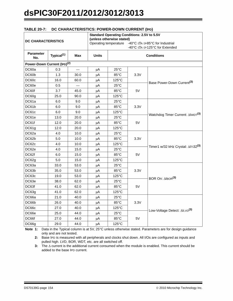
dsPIC30F2011/2012/3012/3013
TABLE 20-7: DC CHARACTERISTICS: POWER-DOWN CURRENT (IPD)
DC CHARACTERISTICS
Standard Operating Conditions: 2.5V to 5.5V(unless otherwise stated)Operating temperature -40°C ≤ TA ≤ +85°C for Industrial
-40°C ≤ TA ≤ +125°C for Extended
Parameter No. Typical(1) Max Units Conditions
Power-Down Current (IPD)(2)
DC60a 0.3 — μA 25°C3.3V
Base Power-Down Current(3)
DC60b 1.3 30.0 μA 85°CDC60c 16.0 60.0 μA 125°CDC60e 0.5 — μA 25°C
5VDC60f 3.7 45.0 μA 85°CDC60g 25.0 90.0 μA 125°CDC61a 6.0 9.0 μA 25°C
3.3V
Watchdog Timer Current: ΔIWDT(3)
DC61b 6.0 9.0 μA 85°CDC61c 6.0 9.0 μA 125°CDC61e 13.0 20.0 μA 25°C
5VDC61f 12.0 20.0 μA 85°CDC61g 12.0 20.0 μA 125°CDC62a 4.0 10.0 μA 25°C
3.3V
Timer1 w/32 kHz Crystal: ΔITI32(3)
DC62b 5.0 10.0 μA 85°CDC62c 4.0 10.0 μA 125°CDC62e 4.0 15.0 μA 25°C
5VDC62f 6.0 15.0 μA 85°CDC62g 5.0 15.0 μA 125°CDC63a 33.0 53.0 μA 25°C
3.3V
BOR On: ΔIBOR(3)
DC63b 35.0 53.0 μA 85°CDC63c 19.0 53.0 μA 125°CDC63e 38.0 62.0 μA 25°C
5VDC63f 41.0 62.0 μA 85°CDC63g 41.0 62.0 μA 125°CDC66a 21.0 40.0 μA 25°C
3.3V
Low-Voltage Detect: ΔILVD(3)
DC66b 26.0 40.0 μA 85°CDC66c 27.0 40.0 μA 125°CDC66e 25.0 44.0 μA 25°C
5VDC66f 27.0 44.0 μA 85°CDC66g 29.0 44.0 μA 125°CNote 1: Data in the Typical column is at 5V, 25°C unless otherwise stated. Parameters are for design guidance
only and are not tested.2: Base IPD is measured with all peripherals and clocks shut down. All I/Os are configured as inputs and
pulled high. LVD, BOR, WDT, etc. are all switched off.3: The Δ current is the additional current consumed when the module is enabled. This current should be
added to the base IPD current.
DS70139G-page 154 © 2010 Microchip Technology Inc.
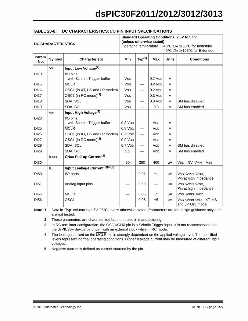
dsPIC30F2011/2012/3012/3013
TABLE 20-8: DC CHARACTERISTICS: I/O PIN INPUT SPECIFICATIONS
DC CHARACTERISTICS
Standard Operating Conditions: 2.5V to 5.5V(unless otherwise stated)Operating temperature -40°C ≤ TA ≤ +85°C for Industrial
-40°C ≤ TA ≤ +125°C for Extended
Param No. Symbol Characteristic Min Typ(1) Max Units Conditions
VIL Input Low Voltage(2)
DI10 I/O pins: with Schmitt Trigger buffer VSS — 0.2 VDD V
DI15 MCLR VSS — 0.2 VDD VDI16 OSC1 (in XT, HS and LP modes) VSS — 0.2 VDD VDI17 OSC1 (in RC mode)(3) VSS — 0.3 VDD VDI18 SDA, SCL VSS — 0.3 VDD V SM bus disabledDI19 SDA, SCL VSS — 0.8 V SM bus enabled
VIH Input High Voltage(2)
DI20 I/O pins: with Schmitt Trigger buffer 0.8 VDD — VDD V
DI25 MCLR 0.8 VDD — VDD VDI26 OSC1 (in XT, HS and LP modes) 0.7 VDD — VDD VDI27 OSC1 (in RC mode)(3) 0.9 VDD — VDD VDI28 SDA, SCL 0.7 VDD — VDD V SM bus disabledDI29 SDA, SCL 2.1 — VDD V SM bus enabled
ICNPU CNXX Pull-up Current(2)
DI30 50 250 400 μA VDD = 5V, VPIN = VSS
IIL Input Leakage Current(2)(4)(5)
DI50 I/O ports — 0.01 ±1 μA VSS ≤ VPIN ≤ VDD,Pin at high impedance
DI51 Analog input pins — 0.50 — μA VSS ≤ VPIN ≤ VDD,Pin at high impedance
DI55 MCLR — 0.05 ±5 μA VSS ≤ VPIN ≤ VDD
DI56 OSC1 — 0.05 ±5 μA VSS ≤ VPIN ≤ VDD, XT, HSand LP Osc mode
Note 1: Data in “Typ” column is at 5V, 25°C unless otherwise stated. Parameters are for design guidance only and are not tested.
2: These parameters are characterized but not tested in manufacturing.3: In RC oscillator configuration, the OSC1/CLKl pin is a Schmitt Trigger input. It is not recommended that
the dsPIC30F device be driven with an external clock while in RC mode.4: The leakage current on the MCLR pin is strongly dependent on the applied voltage level. The specified
levels represent normal operating conditions. Higher leakage current may be measured at different input voltages.
5: Negative current is defined as current sourced by the pin.
© 2010 Microchip Technology Inc. DS70139G-page 155
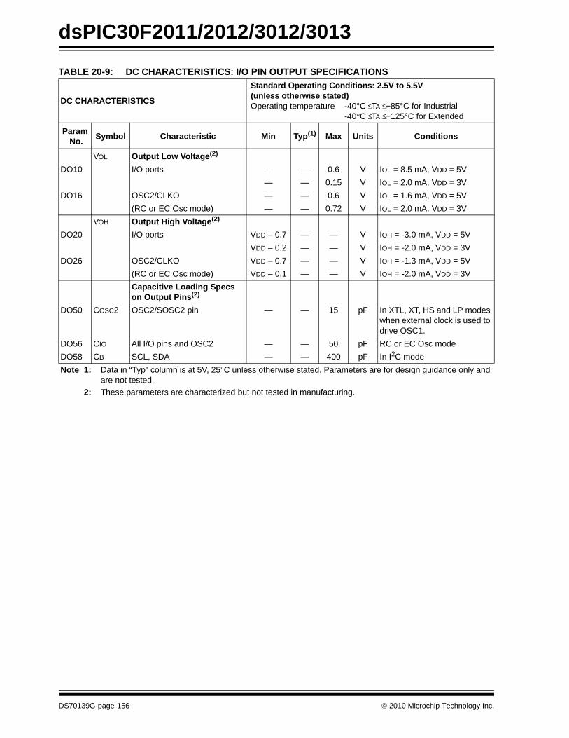
dsPIC30F2011/2012/3012/3013
TABLE 20-9: DC CHARACTERISTICS: I/O PIN OUTPUT SPECIFICATIONS
DC CHARACTERISTICS
Standard Operating Conditions: 2.5V to 5.5V(unless otherwise stated)Operating temperature -40°C ≤ TA ≤ +85°C for Industrial
-40°C ≤ TA ≤ +125°C for Extended
Param No. Symbol Characteristic Min Typ(1) Max Units Conditions
VOL Output Low Voltage(2)
DO10 I/O ports — — 0.6 V IOL = 8.5 mA, VDD = 5V— — 0.15 V IOL = 2.0 mA, VDD = 3V
DO16 OSC2/CLKO — — 0.6 V IOL = 1.6 mA, VDD = 5V(RC or EC Osc mode) — — 0.72 V IOL = 2.0 mA, VDD = 3V
VOH Output High Voltage(2)
DO20 I/O ports VDD – 0.7 — — V IOH = -3.0 mA, VDD = 5VVDD – 0.2 — — V IOH = -2.0 mA, VDD = 3V
DO26 OSC2/CLKO VDD – 0.7 — — V IOH = -1.3 mA, VDD = 5V(RC or EC Osc mode) VDD – 0.1 — — V IOH = -2.0 mA, VDD = 3VCapacitive Loading Specs on Output Pins(2)
DO50 COSC2 OSC2/SOSC2 pin — — 15 pF In XTL, XT, HS and LP modes when external clock is used to drive OSC1.
DO56 CIO All I/O pins and OSC2 — — 50 pF RC or EC Osc mode DO58 CB SCL, SDA — — 400 pF In I2C modeNote 1: Data in “Typ” column is at 5V, 25°C unless otherwise stated. Parameters are for design guidance only and
are not tested.2: These parameters are characterized but not tested in manufacturing.
DS70139G-page 156 © 2010 Microchip Technology Inc.
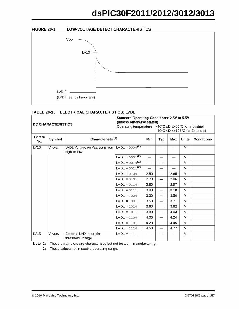
dsPIC30F2011/2012/3012/3013
FIGURE 20-1: LOW-VOLTAGE DETECT CHARACTERISTICSTABLE 20-10: ELECTRICAL CHARACTERISTICS: LVDL
DC CHARACTERISTICS
Standard Operating Conditions: 2.5V to 5.5V(unless otherwise stated)Operating temperature -40°C ≤ TA ≤ +85°C for Industrial
-40°C ≤ TA ≤ +125°C for Extended
ParamNo. Symbol Characteristic(1) Min Typ Max Units Conditions
LV10 VPLVD LVDL Voltage on VDD transition high-to-low
LVDL = 0000(2) — — — V
LVDL = 0001(2) — — — VLVDL = 0010(2) — — — VLVDL = 0011(2) — — — VLVDL = 0100 2.50 — 2.65 VLVDL = 0101 2.70 — 2.86 VLVDL = 0110 2.80 — 2.97 VLVDL = 0111 3.00 — 3.18 VLVDL = 1000 3.30 — 3.50 VLVDL = 1001 3.50 — 3.71 VLVDL = 1010 3.60 — 3.82 VLVDL = 1011 3.80 — 4.03 VLVDL = 1100 4.00 — 4.24 VLVDL = 1101 4.20 — 4.45 VLVDL = 1110 4.50 — 4.77 V
LV15 VLVDIN External LVD input pinthreshold voltage
LVDL = 1111 — — — V
Note 1: These parameters are characterized but not tested in manufacturing.2: These values not in usable operating range.
LV10
LVDIF
VDD
(LVDIF set by hardware)
© 2010 Microchip Technology Inc. DS70139G-page 157
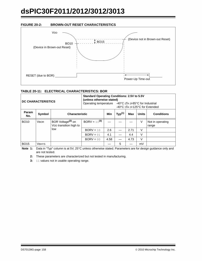
dsPIC30F2011/2012/3012/3013
FIGURE 20-2: BROWN-OUT RESET CHARACTERISTICSTABLE 20-11: ELECTRICAL CHARACTERISTICS: BOR
DC CHARACTERISTICS
Standard Operating Conditions: 2.5V to 5.5V(unless otherwise stated)Operating temperature -40°C ≤ TA ≤ +85°C for Industrial
-40°C ≤ TA ≤ +125°C for Extended
ParamNo. Symbol Characteristic Min Typ(1) Max Units Conditions
BO10 VBOR BOR Voltage(2) on VDD transition high to low
BORV = 11(3) — — — V Not in operating range
BORV = 10 2.6 — 2.71 VBORV = 01 4.1 — 4.4 VBORV = 00 4.58 — 4.73 V
BO15 VBHYS — 5 — mVNote 1: Data in “Typ” column is at 5V, 25°C unless otherwise stated. Parameters are for design guidance only and
are not tested.2: These parameters are characterized but not tested in manufacturing.3: 11 values not in usable operating range.
BO10
RESET (due to BOR)
VDD
(Device in Brown-out Reset)
(Device not in Brown-out Reset)
Power-Up Time-out
BO15
DS70139G-page 158 © 2010 Microchip Technology Inc.
dsPIC30F2011/2012/3012/3013
TABLE 20-12: DC CHARACTERISTICS: PROGRAM AND EEPROM
DC CHARACTERISTICS
Standard Operating Conditions: 2.5V to 5.5V(unless otherwise stated)Operating temperature -40°C ≤ TA ≤ +85°C for Industrial
-40°C ≤ TA ≤ +125°C for Extended
ParamNo. Symbol Characteristic Min Typ(1) Max Units Conditions
Data EEPROM Memory(2)
D120 ED Byte Endurance 100K 1M — E/W -40° C ≤ TA ≤ +85°CD121 VDRW VDD for Read/Write VMIN — 5.5 V Using EECON to Read/Write
VMIN = Minimum operating voltage
D122 TDEW Erase/Write Cycle Time 0.8 2 2.6 ms RTSPD123 TRETD Characteristic Retention 40 100 — Year Provided no other specifications
are violatedD124 IDEW IDD During Programming — 10 30 mA Row Erase
Program Flash Memory(2)
D130 EP Cell Endurance 10K 100K — E/W -40° C ≤ TA ≤ +85°CD131 VPR VDD for Read VMIN — 5.5 V VMIN = Minimum operating
voltageD132 VEB VDD for Bulk Erase 4.5 — 5.5 VD133 VPEW VDD for Erase/Write 3.0 — 5.5 VD134 TPEW Erase/Write Cycle Time 0.8 2 2.6 ms RTSPD135 TRETD Characteristic Retention 40 100 — Year Provided no other specifications
are violatedD137 IPEW IDD During Programming — 10 30 mA Row EraseD138 IEB IDD During Programming — 10 30 mA Bulk EraseNote 1: Data in “Typ” column is at 5V, 25°C unless otherwise stated.
2: These parameters are characterized but not tested in manufacturing.
© 2010 Microchip Technology Inc. DS70139G-page 159
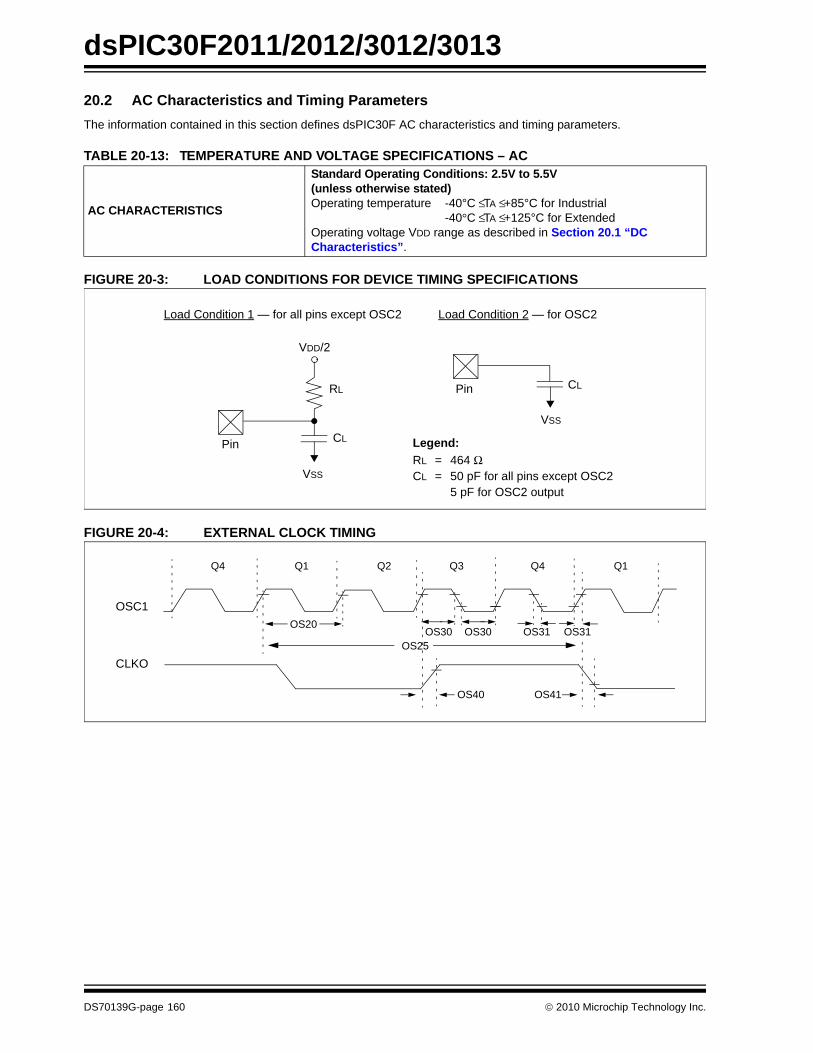
dsPIC30F2011/2012/3012/3013
20.2 AC Characteristics and Timing Parameters The information contained in this section defines dsPIC30F AC characteristics and timing parameters.TABLE 20-13: TEMPERATURE AND VOLTAGE SPECIFICATIONS – AC
FIGURE 20-3: LOAD CONDITIONS FOR DEVICE TIMING SPECIFICATIONS
FIGURE 20-4: EXTERNAL CLOCK TIMING
AC CHARACTERISTICS
Standard Operating Conditions: 2.5V to 5.5V(unless otherwise stated)Operating temperature -40°C ≤ TA ≤ +85°C for Industrial
-40°C ≤ TA ≤ +125°C for ExtendedOperating voltage VDD range as described in Section 20.1 “DC Characteristics”.
VDD/2
CL
RL
Pin
Pin
VSS
VSS
CL
Legend:RL = 464 ΩCL = 50 pF for all pins except OSC2
5 pF for OSC2 output
Load Condition 1 — for all pins except OSC2 Load Condition 2 — for OSC2
OSC1
CLKO
Q4 Q1 Q2 Q3 Q4 Q1
OS20
OS25OS30 OS30
OS40 OS41
OS31 OS31
DS70139G-page 160 © 2010 Microchip Technology Inc.
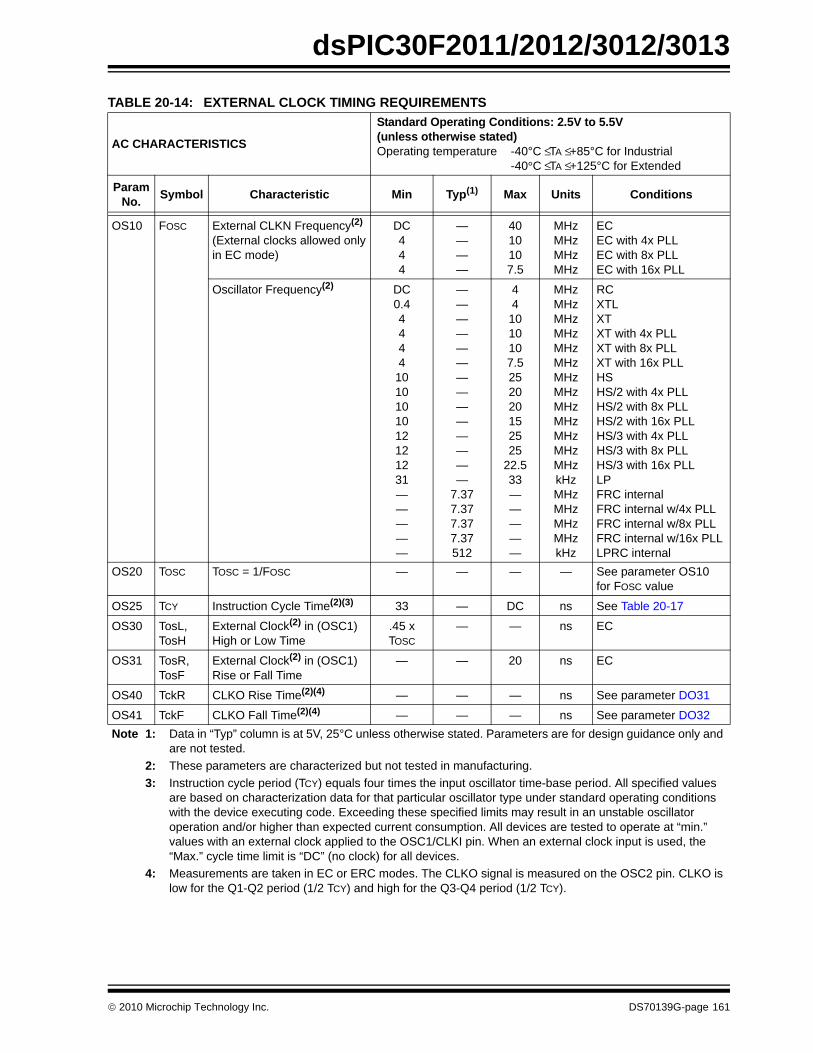
dsPIC30F2011/2012/3012/3013
TABLE 20-14: EXTERNAL CLOCK TIMING REQUIREMENTS
AC CHARACTERISTICS
Standard Operating Conditions: 2.5V to 5.5V(unless otherwise stated)Operating temperature -40°C ≤ TA ≤ +85°C for Industrial
-40°C ≤ TA ≤ +125°C for Extended
ParamNo. Symbol Characteristic Min Typ(1) Max Units Conditions
OS10 FOSC External CLKN Frequency(2)
(External clocks allowed onlyin EC mode)
DC444
————
4010107.5
MHzMHzMHzMHz
ECEC with 4x PLLEC with 8x PLLEC with 16x PLL
Oscillator Frequency(2) DC0.44444
1010101012121231—————
——————————————
7.377.377.377.37512
441010107.5252020152525
22.533—————
MHzMHzMHzMHzMHzMHzMHzMHzMHzMHzMHzMHzMHzkHzMHzMHzMHzMHzkHz
RCXTLXTXT with 4x PLLXT with 8x PLLXT with 16x PLLHSHS/2 with 4x PLLHS/2 with 8x PLLHS/2 with 16x PLLHS/3 with 4x PLLHS/3 with 8x PLLHS/3 with 16x PLLLPFRC internalFRC internal w/4x PLLFRC internal w/8x PLLFRC internal w/16x PLLLPRC internal
OS20 TOSC TOSC = 1/FOSC — — — — See parameter OS10for FOSC value
OS25 TCY Instruction Cycle Time(2)(3) 33 — DC ns See Table 20-17
OS30 TosL,TosH
External Clock(2) in (OSC1)High or Low Time
.45 x TOSC
— — ns EC
OS31 TosR,TosF
External Clock(2) in (OSC1)Rise or Fall Time
— — 20 ns EC
OS40 TckR CLKO Rise Time(2)(4) — — — ns See parameter DO31
OS41 TckF CLKO Fall Time(2)(4) — — — ns See parameter DO32Note 1: Data in “Typ” column is at 5V, 25°C unless otherwise stated. Parameters are for design guidance only and
are not tested.2: These parameters are characterized but not tested in manufacturing.3: Instruction cycle period (TCY) equals four times the input oscillator time-base period. All specified values
are based on characterization data for that particular oscillator type under standard operating conditions with the device executing code. Exceeding these specified limits may result in an unstable oscillator operation and/or higher than expected current consumption. All devices are tested to operate at “min.” values with an external clock applied to the OSC1/CLKI pin. When an external clock input is used, the “Max.” cycle time limit is “DC” (no clock) for all devices.
4: Measurements are taken in EC or ERC modes. The CLKO signal is measured on the OSC2 pin. CLKO is low for the Q1-Q2 period (1/2 TCY) and high for the Q3-Q4 period (1/2 TCY).
© 2010 Microchip Technology Inc. DS70139G-page 161
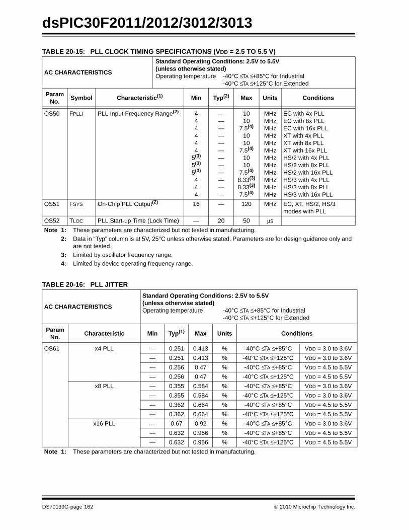
dsPIC30F2011/2012/3012/3013
TABLE 20-15: PLL CLOCK TIMING SPECIFICATIONS (VDD = 2.5 TO 5.5 V)
AC CHARACTERISTICS
Standard Operating Conditions: 2.5V to 5.5V(unless otherwise stated)Operating temperature -40°C ≤ TA ≤ +85°C for Industrial
-40°C ≤ TA ≤ +125°C for Extended
ParamNo. Symbol Characteristic(1) Min Typ(2) Max Units Conditions
OS50 FPLLI PLL Input Frequency Range(2) 444444
5(3)
5(3)
5(3)
444
————————————
1010
7.5(4)
1010
7.5(4)
1010
7.5(4)
8.33(3)
8.33(3)
7.5(4)
MHzMHzMHzMHzMHzMHzMHzMHzMHzMHzMHzMHz
EC with 4x PLL EC with 8x PLL EC with 16x PLL XT with 4x PLLXT with 8x PLLXT with 16x PLLHS/2 with 4x PLLHS/2 with 8x PLLHS/2 with 16x PLLHS/3 with 4x PLLHS/3 with 8x PLLHS/3 with 16x PLL
OS51 FSYS On-Chip PLL Output(2) 16 — 120 MHz EC, XT, HS/2, HS/3 modes with PLL
OS52 TLOC PLL Start-up Time (Lock Time) — 20 50 μsNote 1: These parameters are characterized but not tested in manufacturing.
2: Data in “Typ” column is at 5V, 25°C unless otherwise stated. Parameters are for design guidance only and are not tested.
3: Limited by oscillator frequency range.4: Limited by device operating frequency range.
TABLE 20-16: PLL JITTER
AC CHARACTERISTICS
Standard Operating Conditions: 2.5V to 5.5V(unless otherwise stated)Operating temperature -40°C ≤ TA ≤ +85°C for Industrial
-40°C ≤ TA ≤ +125°C for Extended
Param No. Characteristic Min Typ(1) Max Units Conditions
OS61 x4 PLL — 0.251 0.413 % -40°C ≤ TA ≤ +85°C VDD = 3.0 to 3.6V— 0.251 0.413 % -40°C ≤ TA ≤ +125°C VDD = 3.0 to 3.6V— 0.256 0.47 % -40°C ≤ TA ≤ +85°C VDD = 4.5 to 5.5V— 0.256 0.47 % -40°C ≤ TA ≤ +125°C VDD = 4.5 to 5.5V
x8 PLL — 0.355 0.584 % -40°C ≤ TA ≤ +85°C VDD = 3.0 to 3.6V— 0.355 0.584 % -40°C ≤ TA ≤ +125°C VDD = 3.0 to 3.6V— 0.362 0.664 % -40°C ≤ TA ≤ +85°C VDD = 4.5 to 5.5V— 0.362 0.664 % -40°C ≤ TA ≤ +125°C VDD = 4.5 to 5.5V
x16 PLL — 0.67 0.92 % -40°C ≤ TA ≤ +85°C VDD = 3.0 to 3.6V— 0.632 0.956 % -40°C ≤ TA ≤ +85°C VDD = 4.5 to 5.5V— 0.632 0.956 % -40°C ≤ TA ≤ +125°C VDD = 4.5 to 5.5V
Note 1: These parameters are characterized but not tested in manufacturing.
DS70139G-page 162 © 2010 Microchip Technology Inc.
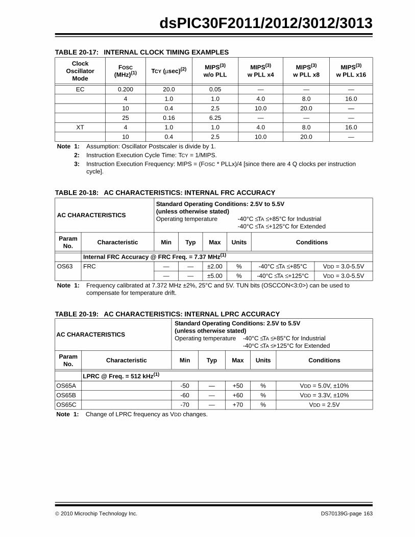
dsPIC30F2011/2012/3012/3013
TABLE 20-17: INTERNAL CLOCK TIMING EXAMPLES Clock
OscillatorMode
FOSC (MHz)(1) TCY (μsec)(2) MIPS(3)
w/o PLLMIPS(3)
w PLL x4MIPS(3)
w PLL x8MIPS(3)
w PLL x16
EC 0.200 20.0 0.05 — — —4 1.0 1.0 4.0 8.0 16.0
10 0.4 2.5 10.0 20.0 —25 0.16 6.25 — — —
XT 4 1.0 1.0 4.0 8.0 16.010 0.4 2.5 10.0 20.0 —
Note 1: Assumption: Oscillator Postscaler is divide by 1.2: Instruction Execution Cycle Time: TCY = 1/MIPS.3: Instruction Execution Frequency: MIPS = (FOSC * PLLx)/4 [since there are 4 Q clocks per instruction
cycle].
TABLE 20-18: AC CHARACTERISTICS: INTERNAL FRC ACCURACY
AC CHARACTERISTICS
Standard Operating Conditions: 2.5V to 5.5V(unless otherwise stated)Operating temperature -40°C ≤ TA ≤ +85°C for Industrial
-40°C ≤ TA ≤ +125°C for Extended
Param No. Characteristic Min Typ Max Units Conditions
Internal FRC Accuracy @ FRC Freq. = 7.37 MHz(1)
OS63 FRC — — ±2.00 % -40°C ≤ TA ≤ +85°C VDD = 3.0-5.5V— — ±5.00 % -40°C ≤ TA ≤ +125°C VDD = 3.0-5.5V
Note 1: Frequency calibrated at 7.372 MHz ±2%, 25°C and 5V. TUN bits (OSCCON<3:0>) can be used to compensate for temperature drift.
TABLE 20-19: AC CHARACTERISTICS: INTERNAL LPRC ACCURACY
AC CHARACTERISTICS
Standard Operating Conditions: 2.5V to 5.5V(unless otherwise stated)Operating temperature -40°C ≤ TA ≤ +85°C for Industrial
-40°C ≤ TA ≤ +125°C for Extended
ParamNo. Characteristic Min Typ Max Units Conditions
LPRC @ Freq. = 512 kHz(1)
OS65A -50 — +50 % VDD = 5.0V, ±10%OS65B -60 — +60 % VDD = 3.3V, ±10%OS65C -70 — +70 % VDD = 2.5VNote 1: Change of LPRC frequency as VDD changes.
© 2010 Microchip Technology Inc. DS70139G-page 163
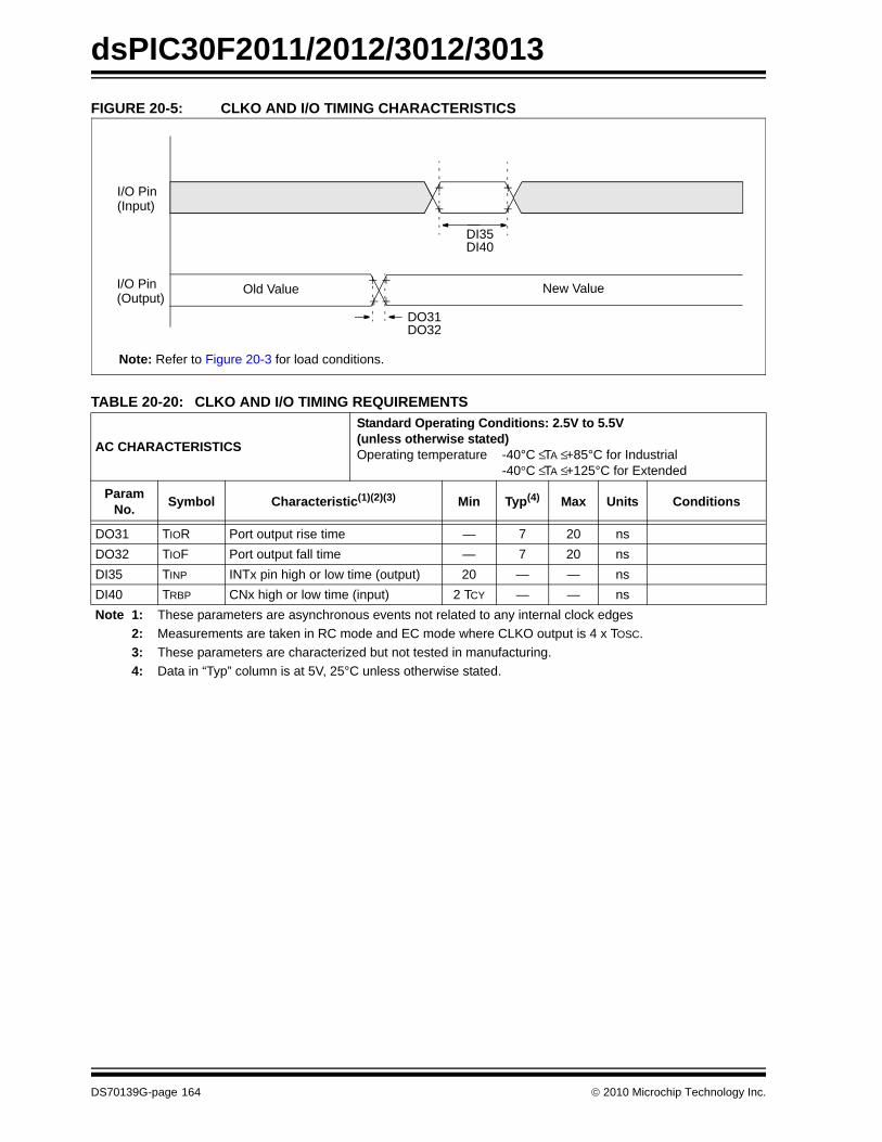
dsPIC30F2011/2012/3012/3013
FIGURE 20-5: CLKO AND I/O TIMING CHARACTERISTICSTABLE 20-20: CLKO AND I/O TIMING REQUIREMENTS
AC CHARACTERISTICS
Standard Operating Conditions: 2.5V to 5.5V(unless otherwise stated)Operating temperature -40°C ≤ TA ≤ +85°C for Industrial
-40°C ≤ TA ≤ +125°C for Extended
ParamNo. Symbol Characteristic(1)(2)(3) Min Typ(4) Max Units Conditions
DO31 TIOR Port output rise time — 7 20 nsDO32 TIOF Port output fall time — 7 20 nsDI35 TINP INTx pin high or low time (output) 20 — — nsDI40 TRBP CNx high or low time (input) 2 TCY — — nsNote 1: These parameters are asynchronous events not related to any internal clock edges
2: Measurements are taken in RC mode and EC mode where CLKO output is 4 x TOSC.3: These parameters are characterized but not tested in manufacturing.4: Data in “Typ” column is at 5V, 25°C unless otherwise stated.
Note: Refer to Figure 20-3 for load conditions.
I/O Pin(Input)
I/O Pin(Output)
DI35
Old Value New Value
DI40
DO31DO32
DS70139G-page 164 © 2010 Microchip Technology Inc.
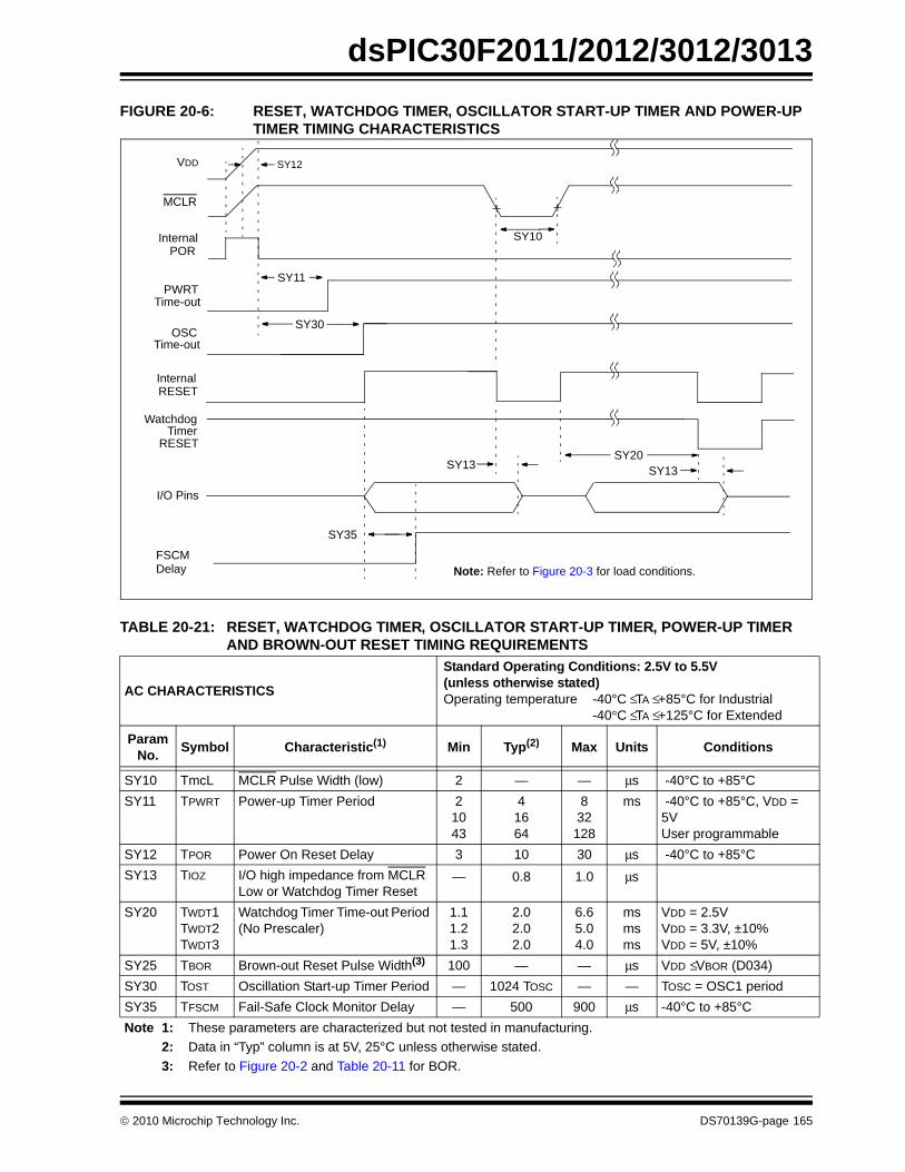
dsPIC30F2011/2012/3012/3013
FIGURE 20-6: RESET, WATCHDOG TIMER, OSCILLATOR START-UP TIMER AND POWER-UPTIMER TIMING CHARACTERISTICS
TABLE 20-21: RESET, WATCHDOG TIMER, OSCILLATOR START-UP TIMER, POWER-UP TIMER AND BROWN-OUT RESET TIMING REQUIREMENTS
AC CHARACTERISTICS
Standard Operating Conditions: 2.5V to 5.5V(unless otherwise stated)Operating temperature -40°C ≤ TA ≤ +85°C for Industrial
-40°C ≤ TA ≤ +125°C for Extended
ParamNo. Symbol Characteristic(1) Min Typ(2) Max Units Conditions
SY10 TmcL MCLR Pulse Width (low) 2 — — μs -40°C to +85°CSY11 TPWRT Power-up Timer Period 2
1043
41664
832
128
ms -40°C to +85°C, VDD = 5VUser programmable
SY12 TPOR Power On Reset Delay 3 10 30 μs -40°C to +85°CSY13 TIOZ I/O high impedance from MCLR
Low or Watchdog Timer Reset— 0.8 1.0 μs
SY20 TWDT1TWDT2TWDT3
Watchdog Timer Time-out Period (No Prescaler)
1.11.21.3
2.02.02.0
6.65.04.0
msmsms
VDD = 2.5VVDD = 3.3V, ±10%VDD = 5V, ±10%
SY25 TBOR Brown-out Reset Pulse Width(3) 100 — — μs VDD ≤ VBOR (D034)SY30 TOST Oscillation Start-up Timer Period — 1024 TOSC — — TOSC = OSC1 periodSY35 TFSCM Fail-Safe Clock Monitor Delay — 500 900 μs -40°C to +85°CNote 1: These parameters are characterized but not tested in manufacturing.
2: Data in “Typ” column is at 5V, 25°C unless otherwise stated.3: Refer to Figure 20-2 and Table 20-11 for BOR.
VDD
MCLR
InternalPOR
PWRTTime-out
OSCTime-out
InternalRESET
WatchdogTimer
RESET
SY11
SY10
SY20SY13
I/O Pins
SY13
Note: Refer to Figure 20-3 for load conditions.FSCM Delay
SY35
SY30
SY12
© 2010 Microchip Technology Inc. DS70139G-page 165
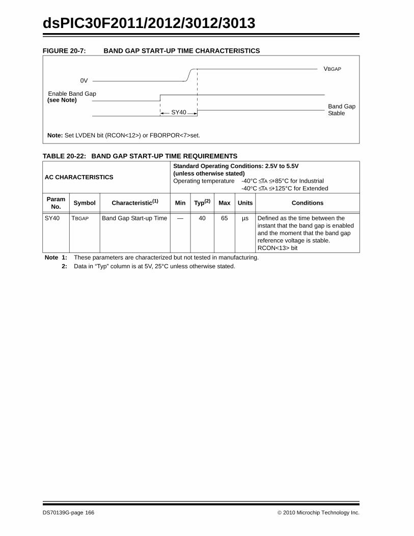
dsPIC30F2011/2012/3012/3013
FIGURE 20-7: BAND GAP START-UP TIME CHARACTERISTICSTABLE 20-22: BAND GAP START-UP TIME REQUIREMENTS
AC CHARACTERISTICS
Standard Operating Conditions: 2.5V to 5.5V(unless otherwise stated)Operating temperature -40°C ≤ TA ≤ +85°C for Industrial
-40°C ≤ TA ≤ +125°C for Extended
ParamNo. Symbol Characteristic(1) Min Typ(2) Max Units Conditions
SY40 TBGAP Band Gap Start-up Time — 40 65 µs Defined as the time between the instant that the band gap is enabled and the moment that the band gap reference voltage is stable. RCON<13> bit
Note 1: These parameters are characterized but not tested in manufacturing.2: Data in “Typ” column is at 5V, 25°C unless otherwise stated.
VBGAP
Enable Band Gap
Band Gap
0V
(see Note)
Stable
Note: Set LVDEN bit (RCON<12>) or FBORPOR<7>set.
SY40
DS70139G-page 166 © 2010 Microchip Technology Inc.
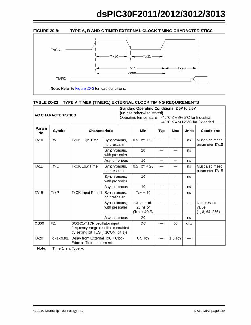
dsPIC30F2011/2012/3012/3013
FIGURE 20-8: TYPE A, B AND C TIMER EXTERNAL CLOCK TIMING CHARACTERISTICSTABLE 20-23: TYPE A TIMER (TIMER1) EXTERNAL CLOCK TIMING REQUIREMENTS
AC CHARACTERISTICS
Standard Operating Conditions: 2.5V to 5.5V(unless otherwise stated)Operating temperature -40°C ≤ TA ≤ +85°C for Industrial
-40°C ≤ TA ≤ +125°C for Extended
ParamNo. Symbol Characteristic Min Typ Max Units Conditions
TA10 TTXH TxCK High Time Synchronous,no prescaler
0.5 TCY + 20 — — ns Must also meet parameter TA15
Synchronous,with prescaler
10 — — ns
Asynchronous 10 — — nsTA11 TTXL TxCK Low Time Synchronous,
no prescaler0.5 TCY + 20 — — ns Must also meet
parameter TA15Synchronous,with prescaler
10 — — ns
Asynchronous 10 — — nsTA15 TTXP TxCK Input Period Synchronous,
no prescalerTCY + 10 — — ns
Synchronous,with prescaler
Greater of:20 ns or
(TCY + 40)/N
— — — N = prescale value(1, 8, 64, 256)
Asynchronous 20 — — nsOS60 Ft1 SOSC1/T1CK oscillator input
frequency range (oscillator enabled by setting bit TCS (T1CON, bit 1))
DC — 50 kHz
TA20 TCKEXTMRL Delay from External TxCK Clock Edge to Timer Increment
0.5 TCY — 1.5 TCY —
Note: Timer1 is a Type A.
Note: Refer to Figure 20-3 for load conditions.
Tx11
Tx15
Tx10
Tx20
TMRX OS60
TxCK
© 2010 Microchip Technology Inc. DS70139G-page 167
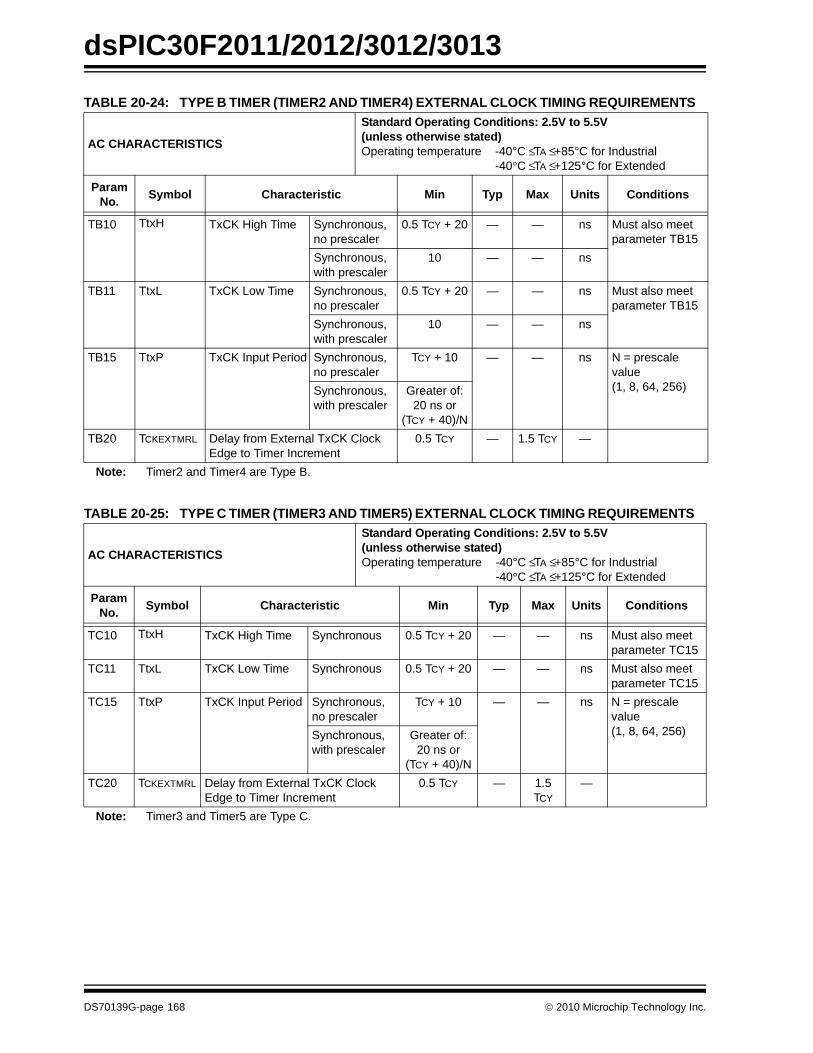
dsPIC30F2011/2012/3012/3013
TABLE 20-24: TYPE B TIMER (TIMER2 AND TIMER4) EXTERNAL CLOCK TIMING REQUIREMENTS
AC CHARACTERISTICS
Standard Operating Conditions: 2.5V to 5.5V(unless otherwise stated)Operating temperature -40°C ≤ TA ≤ +85°C for Industrial
-40°C ≤ TA ≤ +125°C for Extended
ParamNo. Symbol Characteristic Min Typ Max Units Conditions
TB10 TtxH TxCK High Time Synchronous,no prescaler
0.5 TCY + 20 — — ns Must also meet parameter TB15
Synchronous,with prescaler
10 — — ns
TB11 TtxL TxCK Low Time Synchronous,no prescaler
0.5 TCY + 20 — — ns Must also meet parameter TB15
Synchronous,with prescaler
10 — — ns
TB15 TtxP TxCK Input Period Synchronous,no prescaler
TCY + 10 — — ns N = prescale value(1, 8, 64, 256)Synchronous,
with prescalerGreater of:
20 ns or(TCY + 40)/N
TB20 TCKEXTMRL Delay from External TxCK Clock Edge to Timer Increment
0.5 TCY — 1.5 TCY —
Note: Timer2 and Timer4 are Type B.
TABLE 20-25: TYPE C TIMER (TIMER3 AND TIMER5) EXTERNAL CLOCK TIMING REQUIREMENTS
AC CHARACTERISTICS
Standard Operating Conditions: 2.5V to 5.5V(unless otherwise stated)Operating temperature -40°C ≤ TA ≤ +85°C for Industrial
-40°C ≤ TA ≤ +125°C for Extended
ParamNo. Symbol Characteristic Min Typ Max Units Conditions
TC10 TtxH TxCK High Time Synchronous 0.5 TCY + 20 — — ns Must also meet parameter TC15
TC11 TtxL TxCK Low Time Synchronous 0.5 TCY + 20 — — ns Must also meet parameter TC15
TC15 TtxP TxCK Input Period Synchronous,no prescaler
TCY + 10 — — ns N = prescalevalue (1, 8, 64, 256)Synchronous,
with prescalerGreater of:
20 ns or (TCY + 40)/N
TC20 TCKEXTMRL Delay from External TxCK Clock Edge to Timer Increment
0.5 TCY — 1.5 TCY
—
Note: Timer3 and Timer5 are Type C.
DS70139G-page 168 © 2010 Microchip Technology Inc.
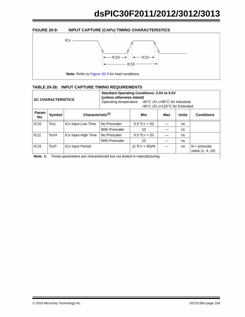
dsPIC30F2011/2012/3012/3013
FIGURE 20-9: INPUT CAPTURE (CAPx) TIMING CHARACTERISTICSTABLE 20-26: INPUT CAPTURE TIMING REQUIREMENTS
AC CHARACTERISTICS
Standard Operating Conditions: 2.5V to 5.5V(unless otherwise stated)Operating temperature -40°C ≤ TA ≤ +85°C for Industrial
-40°C ≤ TA ≤ +125°C for Extended
ParamNo. Symbol Characteristic(1) Min Max Units Conditions
IC10 TccL ICx Input Low Time No Prescaler 0.5 TCY + 20 — nsWith Prescaler 10 — ns
IC11 TccH ICx Input High Time No Prescaler 0.5 TCY + 20 — nsWith Prescaler 10 — ns
IC15 TccP ICx Input Period (2 TCY + 40)/N — ns N = prescale value (1, 4, 16)
Note 1: These parameters are characterized but not tested in manufacturing.
ICX
IC10 IC11
IC15
Note: Refer to Figure 20-3 for load conditions.
© 2010 Microchip Technology Inc. DS70139G-page 169
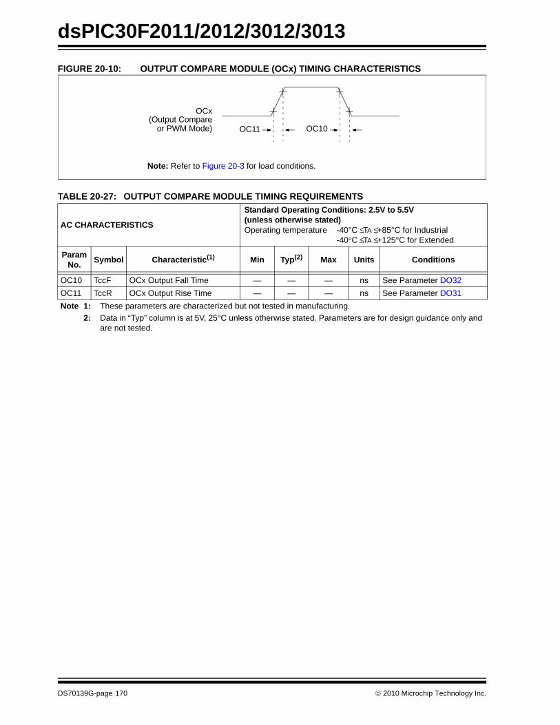
dsPIC30F2011/2012/3012/3013
FIGURE 20-10: OUTPUT COMPARE MODULE (OCx) TIMING CHARACTERISTICSTABLE 20-27: OUTPUT COMPARE MODULE TIMING REQUIREMENTS
AC CHARACTERISTICS
Standard Operating Conditions: 2.5V to 5.5V(unless otherwise stated)Operating temperature -40°C ≤ TA ≤ +85°C for Industrial
-40°C ≤ TA ≤ +125°C for Extended
Param No. Symbol Characteristic(1) Min Typ(2) Max Units Conditions
OC10 TccF OCx Output Fall Time — — — ns See Parameter DO32OC11 TccR OCx Output Rise Time — — — ns See Parameter DO31Note 1: These parameters are characterized but not tested in manufacturing.
2: Data in “Typ” column is at 5V, 25°C unless otherwise stated. Parameters are for design guidance only and are not tested.
OCx
OC11 OC10(Output Compare
Note: Refer to Figure 20-3 for load conditions.
or PWM Mode)
DS70139G-page 170 © 2010 Microchip Technology Inc.
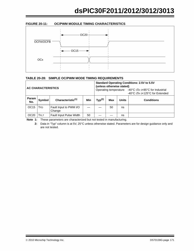
dsPIC30F2011/2012/3012/3013
FIGURE 20-11: OC/PWM MODULE TIMING CHARACTERISTICSTABLE 20-28: SIMPLE OC/PWM MODE TIMING REQUIREMENTS
AC CHARACTERISTICS
Standard Operating Conditions: 2.5V to 5.5V(unless otherwise stated)Operating temperature -40°C ≤ TA ≤ +85°C for Industrial
-40°C ≤ TA ≤ +125°C for Extended
Param No. Symbol Characteristic(1) Min Typ(2) Max Units Conditions
OC15 TFD Fault Input to PWM I/O Change
— — 50 ns
OC20 TFLT Fault Input Pulse Width 50 — — nsNote 1: These parameters are characterized but not tested in manufacturing.
2: Data in “Typ” column is at 5V, 25°C unless otherwise stated. Parameters are for design guidance only and are not tested.
OCFA/OCFB
OCx
OC20
OC15
© 2010 Microchip Technology Inc. DS70139G-page 171
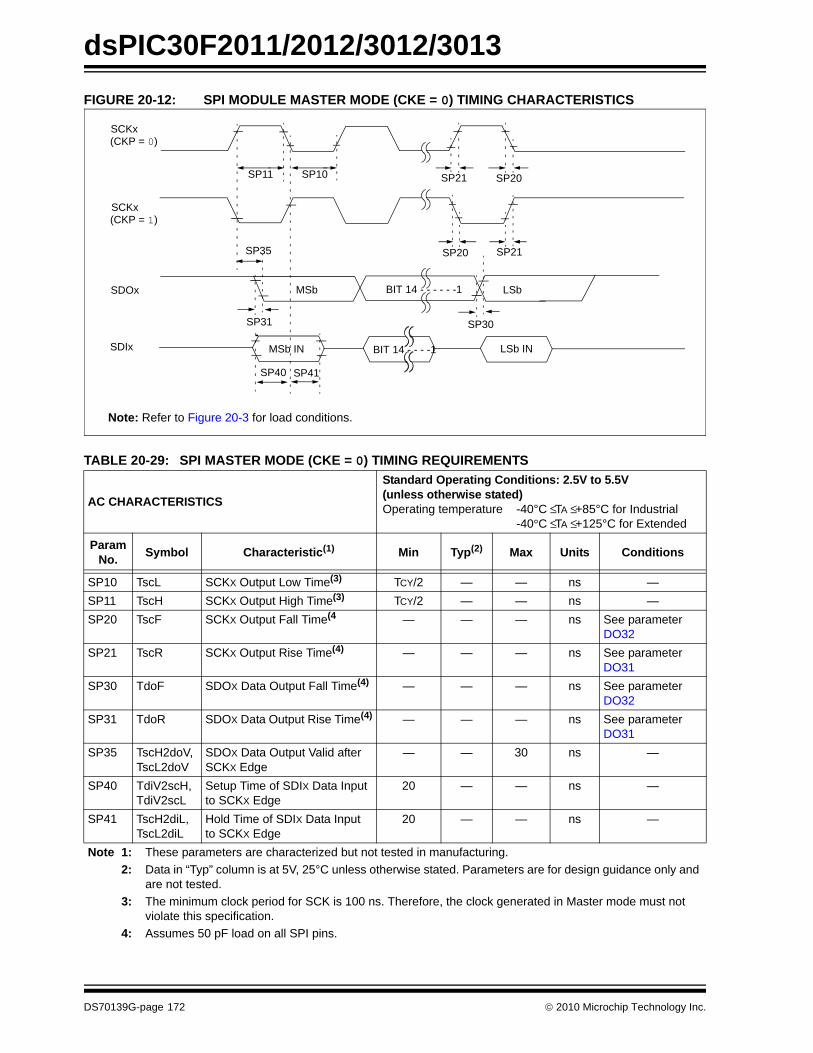
dsPIC30F2011/2012/3012/3013
FIGURE 20-12: SPI MODULE MASTER MODE (CKE = 0) TIMING CHARACTERISTICSTABLE 20-29: SPI MASTER MODE (CKE = 0) TIMING REQUIREMENTS
AC CHARACTERISTICS
Standard Operating Conditions: 2.5V to 5.5V(unless otherwise stated)Operating temperature -40°C ≤ TA ≤ +85°C for Industrial
-40°C ≤ TA ≤ +125°C for Extended
ParamNo. Symbol Characteristic(1) Min Typ(2) Max Units Conditions
SP10 TscL SCKX Output Low Time(3) TCY/2 — — ns —SP11 TscH SCKX Output High Time(3) TCY/2 — — ns —SP20 TscF SCKX Output Fall Time(4 — — — ns See parameter
DO32SP21 TscR SCKX Output Rise Time(4) — — — ns See parameter
DO31SP30 TdoF SDOX Data Output Fall Time(4) — — — ns See parameter
DO32SP31 TdoR SDOX Data Output Rise Time(4) — — — ns See parameter
DO31SP35 TscH2doV,
TscL2doVSDOX Data Output Valid after SCKX Edge
— — 30 ns —
SP40 TdiV2scH,TdiV2scL
Setup Time of SDIX Data Inputto SCKX Edge
20 — — ns —
SP41 TscH2diL,TscL2diL
Hold Time of SDIX Data Inputto SCKX Edge
20 — — ns —
Note 1: These parameters are characterized but not tested in manufacturing.2: Data in “Typ” column is at 5V, 25°C unless otherwise stated. Parameters are for design guidance only and
are not tested.3: The minimum clock period for SCK is 100 ns. Therefore, the clock generated in Master mode must not
violate this specification.4: Assumes 50 pF load on all SPI pins.
SCKx(CKP = 0)
SCKx(CKP = 1)
SDOx
SDIx
SP11 SP10
SP40 SP41
SP21SP20SP35
SP20SP21
MSb LSbBIT 14 - - - - - -1
MSb IN LSb INBIT 14 - - - -1
SP30SP31
Note: Refer to Figure 20-3 for load conditions.
DS70139G-page 172 © 2010 Microchip Technology Inc.
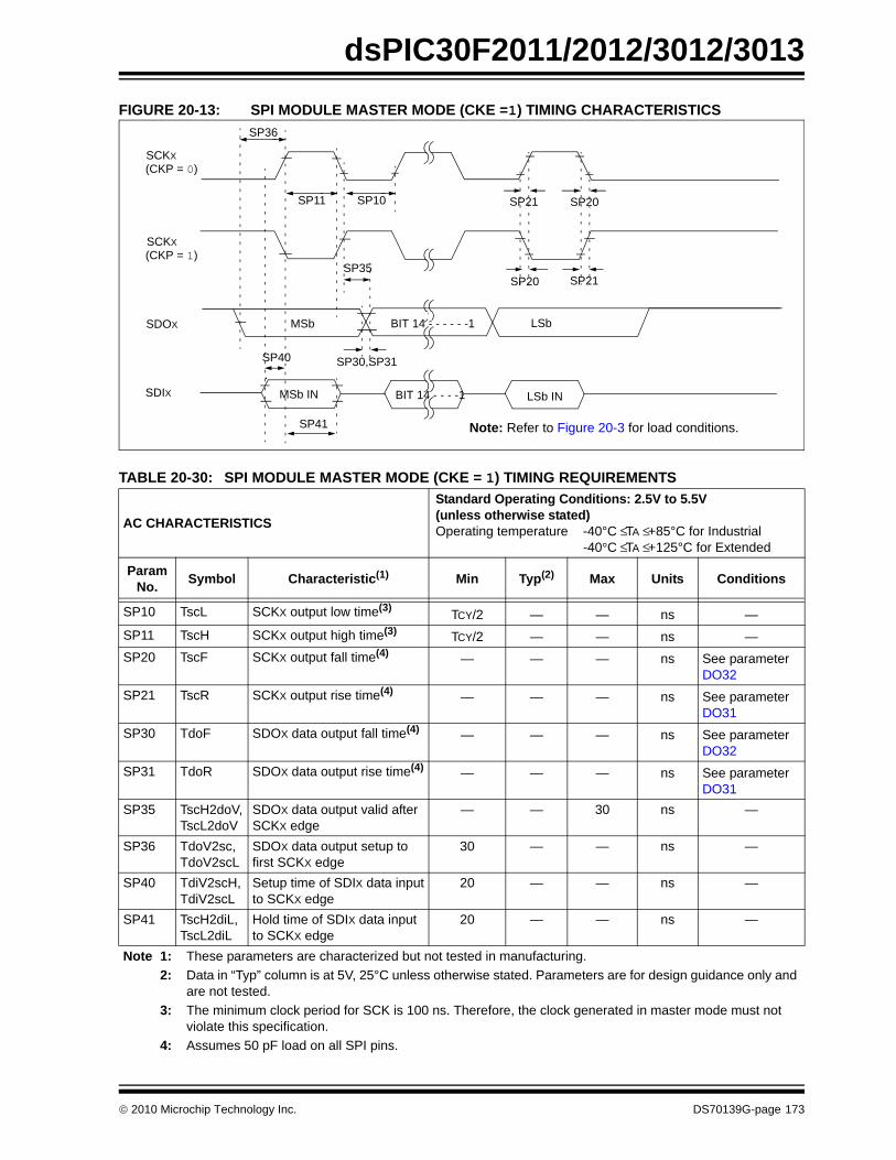
dsPIC30F2011/2012/3012/3013
FIGURE 20-13: SPI MODULE MASTER MODE (CKE =1) TIMING CHARACTERISTICSTABLE 20-30: SPI MODULE MASTER MODE (CKE = 1) TIMING REQUIREMENTS
AC CHARACTERISTICS
Standard Operating Conditions: 2.5V to 5.5V(unless otherwise stated)Operating temperature -40°C ≤ TA ≤ +85°C for Industrial
-40°C ≤ TA ≤ +125°C for Extended
ParamNo. Symbol Characteristic(1) Min Typ(2) Max Units Conditions
SP10 TscL SCKX output low time(3) TCY/2 — — ns —SP11 TscH SCKX output high time(3) TCY/2 — — ns —SP20 TscF SCKX output fall time(4) — — — ns See parameter
DO32SP21 TscR SCKX output rise time(4) — — — ns See parameter
DO31SP30 TdoF SDOX data output fall time(4) — — — ns See parameter
DO32SP31 TdoR SDOX data output rise time(4) — — — ns See parameter
DO31SP35 TscH2doV,
TscL2doVSDOX data output valid afterSCKX edge
— — 30 ns —
SP36 TdoV2sc, TdoV2scL
SDOX data output setup tofirst SCKX edge
30 — — ns —
SP40 TdiV2scH, TdiV2scL
Setup time of SDIX data inputto SCKX edge
20 — — ns —
SP41 TscH2diL, TscL2diL
Hold time of SDIX data inputto SCKX edge
20 — — ns —
Note 1: These parameters are characterized but not tested in manufacturing.2: Data in “Typ” column is at 5V, 25°C unless otherwise stated. Parameters are for design guidance only and
are not tested.3: The minimum clock period for SCK is 100 ns. Therefore, the clock generated in master mode must not
violate this specification.4: Assumes 50 pF load on all SPI pins.
SCKX(CKP = 0)
SCKX(CKP = 1)
SDOX
SDIX
SP36
SP30,SP31
SP35
MSb
MSb IN
BIT 14 - - - - - -1
LSb INBIT 14 - - - -1
LSb
Note: Refer to Figure 20-3 for load conditions.
SP11 SP10 SP20SP21
SP21SP20
SP40
SP41
© 2010 Microchip Technology Inc. DS70139G-page 173
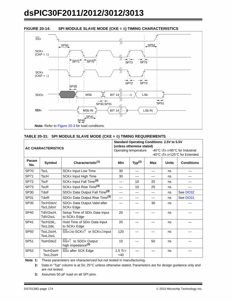
dsPIC30F2011/2012/3012/3013
FIGURE 20-14: SPI MODULE SLAVE MODE (CKE = 0) TIMING CHARACTERISTICSTABLE 20-31: SPI MODULE SLAVE MODE (CKE = 0) TIMING REQUIREMENTS
AC CHARACTERISTICS
Standard Operating Conditions: 2.5V to 5.5V(unless otherwise stated)Operating temperature -40°C ≤ TA ≤ +85°C for Industrial
-40°C ≤ TA ≤ +125°C for Extended
ParamNo. Symbol Characteristic(1) Min Typ(2) Max Units Conditions
SP70 TscL SCKX Input Low Time 30 — — ns —SP71 TscH SCKX Input High Time 30 — — ns —SP72 TscF SCKX Input Fall Time(3) — 10 25 ns —SP73 TscR SCKX Input Rise Time(3) — 10 25 ns —SP30 TdoF SDOX Data Output Fall Time(3) — — — ns See DO32SP31 TdoR SDOX Data Output Rise Time(3) — — — ns See DO31SP35 TscH2doV,
TscL2doVSDOX Data Output Valid afterSCKX Edge
— — 30 ns —
SP40 TdiV2scH, TdiV2scL
Setup Time of SDIX Data Inputto SCKX Edge
20 — — ns —
SP41 TscH2diL, TscL2diL
Hold Time of SDIX Data Inputto SCKX Edge
20 — — ns —
SP50 TssL2scH, TssL2scL
SSX↓ to SCKX↑ or SCKX↓ Input 120 — — ns —
SP51 TssH2doZ SSX↑ to SDOX Outputhigh impedance(3)
10 — 50 ns —
SP52 TscH2ssHTscL2ssH
SSX after SCK Edge 1.5 TCY +40
— — ns —
Note 1: These parameters are characterized but not tested in manufacturing.2: Data in “Typ” column is at 5V, 25°C unless otherwise stated. Parameters are for design guidance only and
are not tested.3: Assumes 50 pF load on all SPI pins.
SSX
SCKX(CKP = 0)
SCKX(CKP = 1)
SDOX
SDI
SP50
SP40SP41
SP30,SP31 SP51
SP35
SDIX
MSb LSbBIT 14 - - - - - -1
MSb IN BIT 14 - - - -1 LSb IN
SP52
SP73SP72
SP72SP73SP71 SP70
Note: Refer to Figure 20-3 for load conditions.
DS70139G-page 174 © 2010 Microchip Technology Inc.
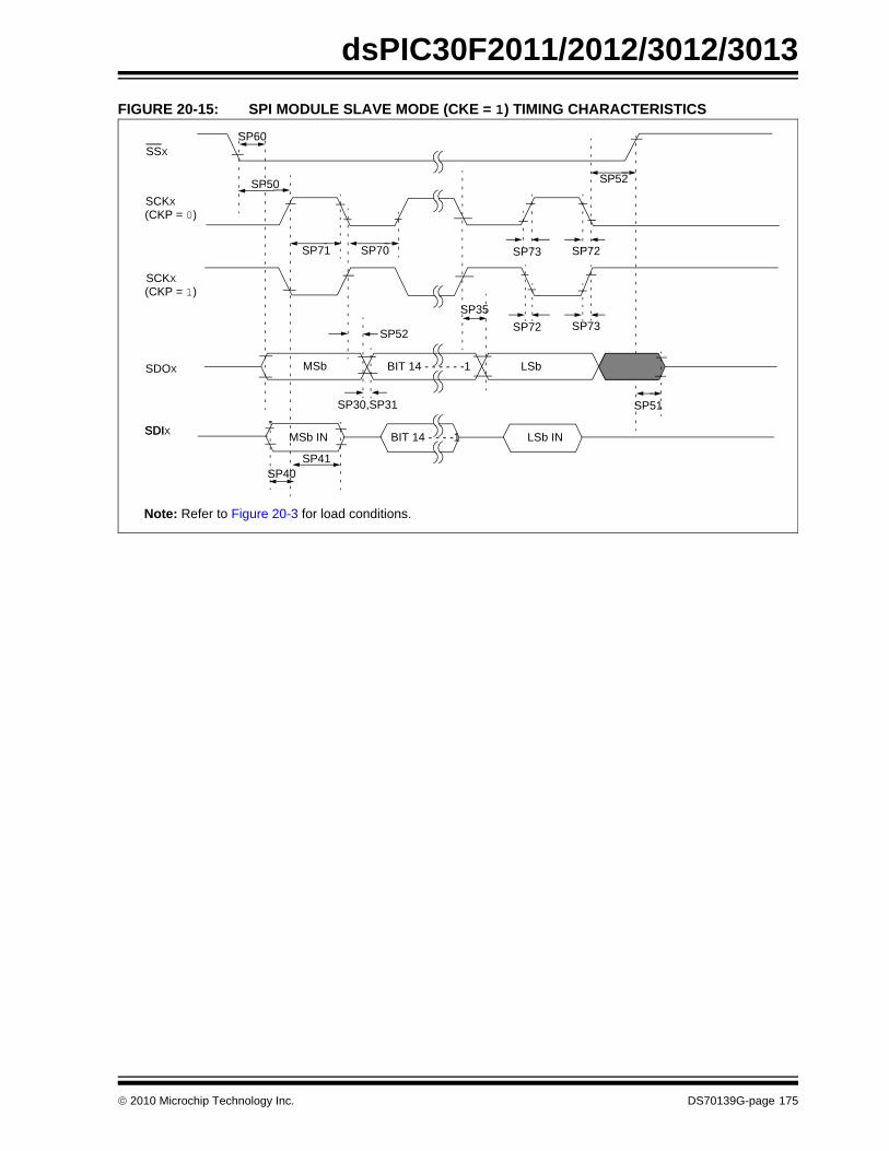
dsPIC30F2011/2012/3012/3013
FIGURE 20-15: SPI MODULE SLAVE MODE (CKE = 1) TIMING CHARACTERISTICSSSX
SCKX(CKP = 0)
SCKX(CKP = 1)
SDOX
SDI
SP50
SP60
SDIX
SP30,SP31
MSb BIT 14 - - - - - -1 LSb
SP51
MSb IN BIT 14 - - - -1 LSb IN
SP35
SP52
SP52
SP73SP72
SP72SP73SP71 SP70
SP40SP41
Note: Refer to Figure 20-3 for load conditions.
© 2010 Microchip Technology Inc. DS70139G-page 175
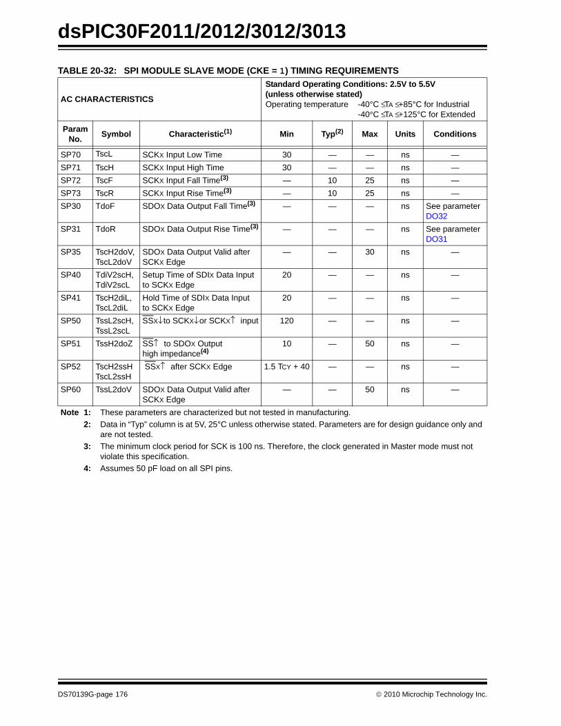
dsPIC30F2011/2012/3012/3013
TABLE 20-32: SPI MODULE SLAVE MODE (CKE = 1) TIMING REQUIREMENTS
AC CHARACTERISTICS
Standard Operating Conditions: 2.5V to 5.5V(unless otherwise stated)Operating temperature -40°C ≤ TA ≤ +85°C for Industrial
-40°C ≤ TA ≤ +125°C for Extended
ParamNo. Symbol Characteristic(1) Min Typ(2) Max Units Conditions
SP70 TscL SCKX Input Low Time 30 — — ns —SP71 TscH SCKX Input High Time 30 — — ns —SP72 TscF SCKX Input Fall Time(3) — 10 25 ns —SP73 TscR SCKX Input Rise Time(3) — 10 25 ns —SP30 TdoF SDOX Data Output Fall Time(3) — — — ns See parameter
DO32SP31 TdoR SDOX Data Output Rise Time(3) — — — ns See parameter
DO31SP35 TscH2doV,
TscL2doVSDOX Data Output Valid afterSCKX Edge
— — 30 ns —
SP40 TdiV2scH, TdiV2scL
Setup Time of SDIX Data Inputto SCKX Edge
20 — — ns —
SP41 TscH2diL, TscL2diL
Hold Time of SDIX Data Inputto SCKX Edge
20 — — ns —
SP50 TssL2scH, TssL2scL
SSX↓ to SCKX↓ or SCKX↑ input 120 — — ns —
SP51 TssH2doZ SS↑ to SDOX Outputhigh impedance(4)
10 — 50 ns —
SP52 TscH2ssHTscL2ssH
SSX↑ after SCKX Edge 1.5 TCY + 40 — — ns —
SP60 TssL2doV SDOX Data Output Valid afterSCKX Edge
— — 50 ns —
Note 1: These parameters are characterized but not tested in manufacturing.2: Data in “Typ” column is at 5V, 25°C unless otherwise stated. Parameters are for design guidance only and
are not tested.3: The minimum clock period for SCK is 100 ns. Therefore, the clock generated in Master mode must not
violate this specification.4: Assumes 50 pF load on all SPI pins.
DS70139G-page 176 © 2010 Microchip Technology Inc.
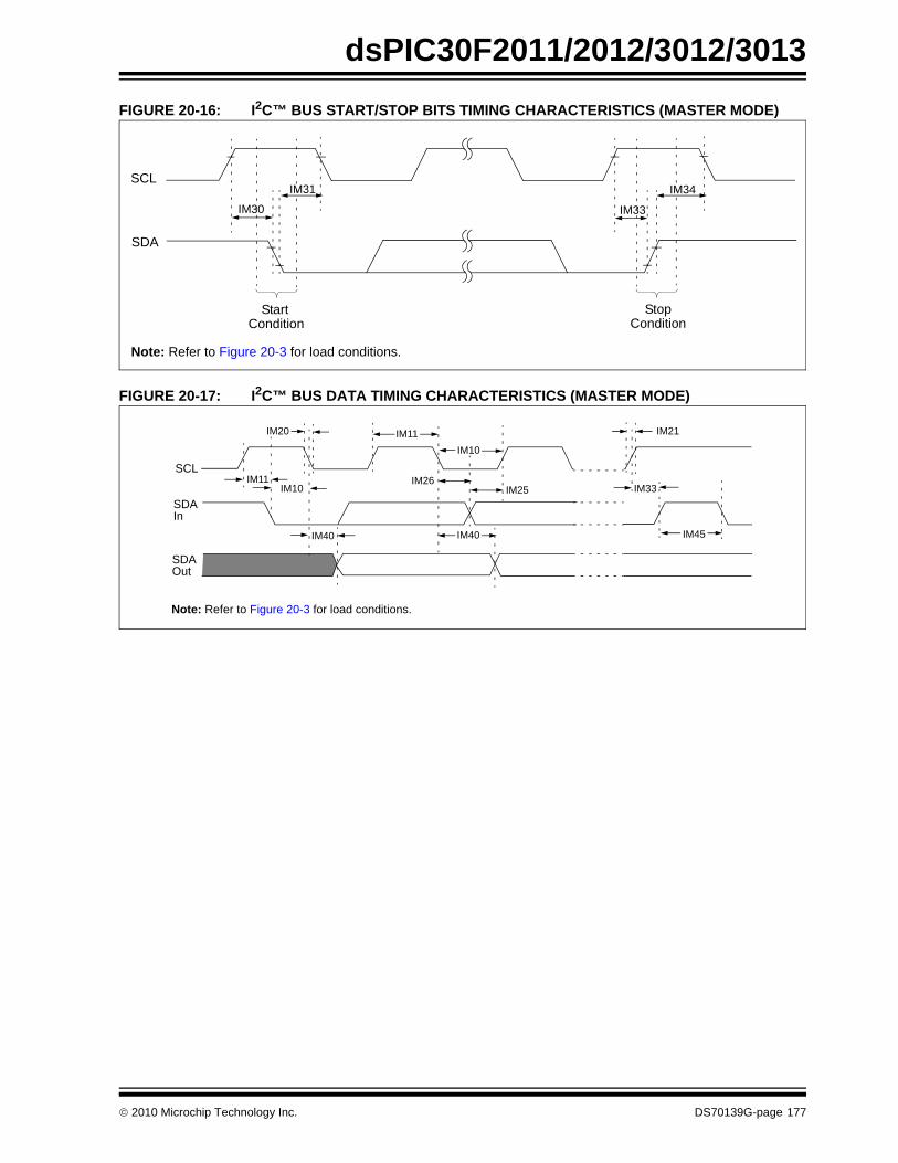
dsPIC30F2011/2012/3012/3013
FIGURE 20-16: I2C™ BUS START/STOP BITS TIMING CHARACTERISTICS (MASTER MODE)FIGURE 20-17: I2C™ BUS DATA TIMING CHARACTERISTICS (MASTER MODE)
IM31 IM34SCL
SDA
StartCondition
StopCondition
IM30 IM33
Note: Refer to Figure 20-3 for load conditions.
IM11IM10 IM33
IM11IM10
IM20
IM26IM25
IM40 IM40 IM45
IM21
SCL
SDAIn
SDAOut
Note: Refer to Figure 20-3 for load conditions.
© 2010 Microchip Technology Inc. DS70139G-page 177
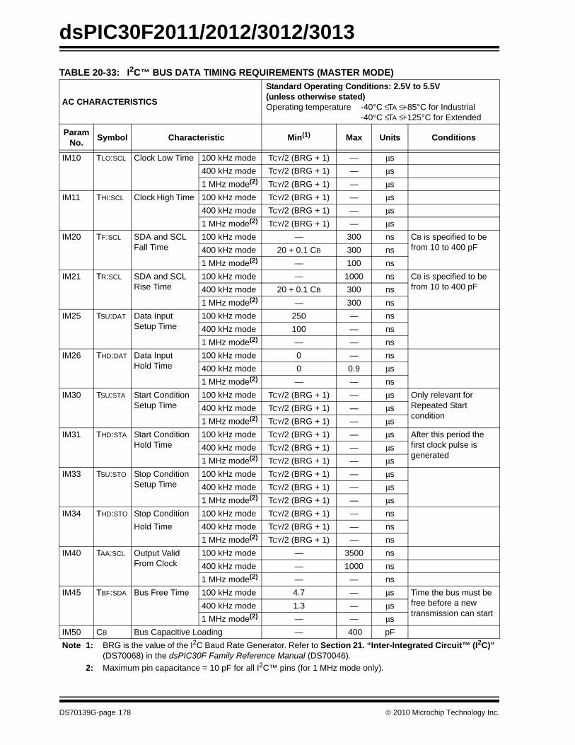
dsPIC30F2011/2012/3012/3013
ITABLE 20-33: I2C™ BUS DATA TIMING REQUIREMENTS (MASTER MODE)
AC CHARACTERISTICS
Standard Operating Conditions: 2.5V to 5.5V(unless otherwise stated)Operating temperature -40°C ≤ TA ≤ +85°C for Industrial
-40°C ≤ TA ≤ +125°C for Extended
ParamNo. Symbol Characteristic Min(1) Max Units Conditions
IM10 TLO:SCL Clock Low Time 100 kHz mode TCY/2 (BRG + 1) — μs400 kHz mode TCY/2 (BRG + 1) — μs1 MHz mode(2) TCY/2 (BRG + 1) — μs
IM11 THI:SCL Clock High Time 100 kHz mode TCY/2 (BRG + 1) — μs400 kHz mode TCY/2 (BRG + 1) — μs1 MHz mode(2) TCY/2 (BRG + 1) — μs
IM20 TF:SCL SDA and SCLFall Time
100 kHz mode — 300 ns CB is specified to be from 10 to 400 pF400 kHz mode 20 + 0.1 CB 300 ns
1 MHz mode(2) — 100 nsIM21 TR:SCL SDA and SCL
Rise Time100 kHz mode — 1000 ns CB is specified to be
from 10 to 400 pF400 kHz mode 20 + 0.1 CB 300 ns1 MHz mode(2) — 300 ns
IM25 TSU:DAT Data InputSetup Time
100 kHz mode 250 — ns400 kHz mode 100 — ns1 MHz mode(2) — — ns
IM26 THD:DAT Data InputHold Time
100 kHz mode 0 — ns400 kHz mode 0 0.9 μs1 MHz mode(2) — — ns
IM30 TSU:STA Start ConditionSetup Time
100 kHz mode TCY/2 (BRG + 1) — μs Only relevant for Repeated Startcondition
400 kHz mode TCY/2 (BRG + 1) — μs1 MHz mode(2) TCY/2 (BRG + 1) — μs
IM31 THD:STA Start Condition Hold Time
100 kHz mode TCY/2 (BRG + 1) — μs After this period thefirst clock pulse isgenerated
400 kHz mode TCY/2 (BRG + 1) — μs1 MHz mode(2) TCY/2 (BRG + 1) — μs
IM33 TSU:STO Stop Condition Setup Time
100 kHz mode TCY/2 (BRG + 1) — μs400 kHz mode TCY/2 (BRG + 1) — μs1 MHz mode(2) TCY/2 (BRG + 1) — μs
IM34 THD:STO Stop Condition 100 kHz mode TCY/2 (BRG + 1) — nsHold Time 400 kHz mode TCY/2 (BRG + 1) — ns
1 MHz mode(2) TCY/2 (BRG + 1) — nsIM40 TAA:SCL Output Valid
From Clock100 kHz mode — 3500 ns400 kHz mode — 1000 ns1 MHz mode(2) — — ns
IM45 TBF:SDA Bus Free Time 100 kHz mode 4.7 — μs Time the bus must be free before a newtransmission can start
400 kHz mode 1.3 — μs1 MHz mode(2) — — μs
IM50 CB Bus Capacitive Loading — 400 pF Note 1: BRG is the value of the I2C Baud Rate Generator. Refer to Section 21. “Inter-Integrated Circuit™ (I2C)”
(DS70068) in the dsPIC30F Family Reference Manual (DS70046).2: Maximum pin capacitance = 10 pF for all I2C™ pins (for 1 MHz mode only).
DS70139G-page 178 © 2010 Microchip Technology Inc.
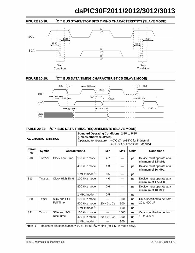
dsPIC30F2011/2012/3012/3013
FIGURE 20-18: I2C™ BUS START/STOP BITS TIMING CHARACTERISTICS (SLAVE MODE)FIGURE 20-19: I2C™ BUS DATA TIMING CHARACTERISTICS (SLAVE MODE)
TABLE 20-34: I2C™ BUS DATA TIMING REQUIREMENTS (SLAVE MODE)
AC CHARACTERISTICS
Standard Operating Conditions: 2.5V to 5.5V(unless otherwise stated)Operating temperature -40°C ≤ TA ≤ +85°C for Industrial
-40°C ≤ TA ≤ +125°C for Extended
ParamNo. Symbol Characteristic Min Max Units Conditions
IS10 TLO:SCL Clock Low Time 100 kHz mode 4.7 — μs Device must operate at a minimum of 1.5 MHz
400 kHz mode 1.3 — μs Device must operate at a minimum of 10 MHz.
1 MHz mode(1) 0.5 — μsIS11 THI:SCL Clock High Time 100 kHz mode 4.0 — μs Device must operate at a
minimum of 1.5 MHz400 kHz mode 0.6 — μs Device must operate at a
minimum of 10 MHz1 MHz mode(1) 0.5 — μs
IS20 TF:SCL SDA and SCLFall Time
100 kHz mode — 300 ns CB is specified to be from10 to 400 pF400 kHz mode 20 + 0.1 CB 300 ns
1 MHz mode(1) — 100 nsIS21 TR:SCL SDA and SCL
Rise Time100 kHz mode — 1000 ns CB is specified to be from
10 to 400 pF400 kHz mode 20 + 0.1 CB 300 ns1 MHz mode(1) — 300 ns
Note 1: Maximum pin capacitance = 10 pF for all I2C™ pins (for 1 MHz mode only).
IS31 IS34SCL
SDA
StartCondition
StopCondition
IS30 IS33
IS30IS31 IS33
IS11
IS10
IS20
IS26IS25
IS40 IS40 IS45
IS21
SCL
SDAIn
SDAOut
© 2010 Microchip Technology Inc. DS70139G-page 179
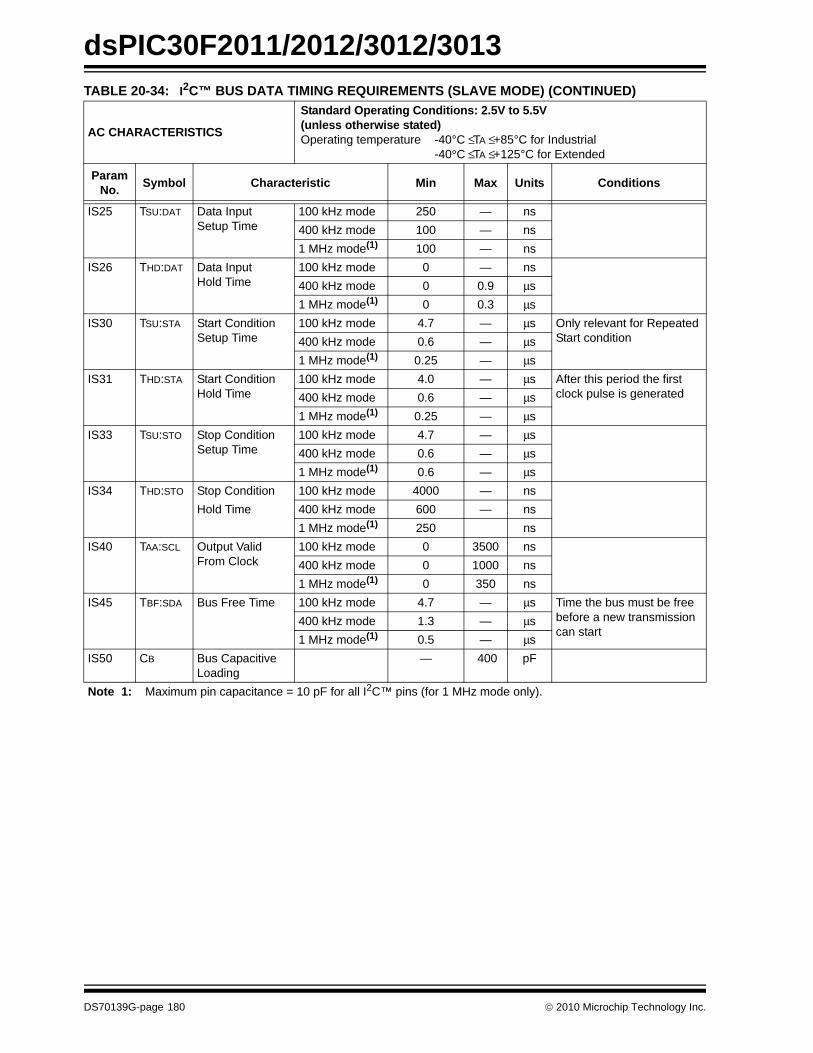
dsPIC30F2011/2012/3012/3013
IS25 TSU:DAT Data InputSetup Time
100 kHz mode 250 — ns400 kHz mode 100 — ns1 MHz mode(1) 100 — ns
IS26 THD:DAT Data InputHold Time
100 kHz mode 0 — ns400 kHz mode 0 0.9 μs1 MHz mode(1) 0 0.3 μs
IS30 TSU:STA Start ConditionSetup Time
100 kHz mode 4.7 — μs Only relevant for Repeated Start condition400 kHz mode 0.6 — μs
1 MHz mode(1) 0.25 — μsIS31 THD:STA Start Condition
Hold Time 100 kHz mode 4.0 — μs After this period the first
clock pulse is generated400 kHz mode 0.6 — μs1 MHz mode(1) 0.25 — μs
IS33 TSU:STO Stop Condition Setup Time
100 kHz mode 4.7 — μs400 kHz mode 0.6 — μs1 MHz mode(1) 0.6 — μs
IS34 THD:STO Stop Condition 100 kHz mode 4000 — nsHold Time 400 kHz mode 600 — ns
1 MHz mode(1) 250 nsIS40 TAA:SCL Output Valid
From Clock100 kHz mode 0 3500 ns400 kHz mode 0 1000 ns1 MHz mode(1) 0 350 ns
IS45 TBF:SDA Bus Free Time 100 kHz mode 4.7 — μs Time the bus must be free before a new transmission can start
400 kHz mode 1.3 — μs1 MHz mode(1) 0.5 — μs
IS50 CB Bus Capacitive Loading
— 400 pF
TABLE 20-34: I2C™ BUS DATA TIMING REQUIREMENTS (SLAVE MODE) (CONTINUED)
AC CHARACTERISTICS
Standard Operating Conditions: 2.5V to 5.5V(unless otherwise stated)Operating temperature -40°C ≤ TA ≤ +85°C for Industrial
-40°C ≤ TA ≤ +125°C for Extended
ParamNo. Symbol Characteristic Min Max Units Conditions
Note 1: Maximum pin capacitance = 10 pF for all I2C™ pins (for 1 MHz mode only).
DS70139G-page 180 © 2010 Microchip Technology Inc.
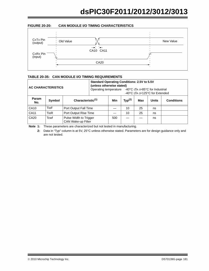
dsPIC30F2011/2012/3012/3013
FIGURE 20-20: CAN MODULE I/O TIMING CHARACTERISTICSTABLE 20-35: CAN MODULE I/O TIMING REQUIREMENTS
AC CHARACTERISTICS
Standard Operating Conditions: 2.5V to 5.5V(unless otherwise stated)Operating temperature -40°C ≤ TA ≤ +85°C for Industrial
-40°C ≤ TA ≤ +125°C for Extended
ParamNo. Symbol Characteristic(1) Min Typ(2) Max Units Conditions
CA10 TioF Port Output Fall Time — 10 25 nsCA11 TioR Port Output Rise Time — 10 25 nsCA20 Tcwf Pulse Width to Trigger
CAN Wake-up Filter500 — — ns
Note 1: These parameters are characterized but not tested in manufacturing.2: Data in “Typ” column is at 5V, 25°C unless otherwise stated. Parameters are for design guidance only and
are not tested.
CXTX Pin(output)
CA10 CA11
Old Value New Value
CA20
CXRX Pin(input)
© 2010 Microchip Technology Inc. DS70139G-page 181
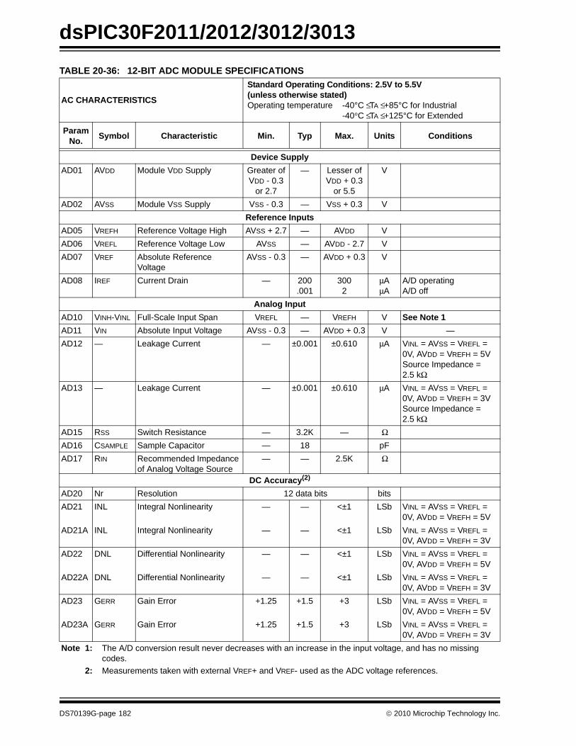
dsPIC30F2011/2012/3012/3013
TABLE 20-36: 12-BIT ADC MODULE SPECIFICATIONSAC CHARACTERISTICS
Standard Operating Conditions: 2.5V to 5.5V(unless otherwise stated)Operating temperature -40°C ≤ TA ≤ +85°C for Industrial
-40°C ≤ TA ≤ +125°C for Extended
Param No. Symbol Characteristic Min. Typ Max. Units Conditions
Device SupplyAD01 AVDD Module VDD Supply Greater of
VDD - 0.3or 2.7
— Lesser ofVDD + 0.3
or 5.5
V
AD02 AVSS Module VSS Supply VSS - 0.3 — VSS + 0.3 VReference Inputs
AD05 VREFH Reference Voltage High AVSS + 2.7 — AVDD VAD06 VREFL Reference Voltage Low AVSS — AVDD - 2.7 VAD07 VREF Absolute Reference
Voltage AVSS - 0.3 — AVDD + 0.3 V
AD08 IREF Current Drain — 200.001
3002
μAμA
A/D operatingA/D off
Analog InputAD10 VINH-VINL Full-Scale Input Span VREFL — VREFH V See Note 1AD11 VIN Absolute Input Voltage AVSS - 0.3 — AVDD + 0.3 V —AD12 — Leakage Current — ±0.001 ±0.610 μA VINL = AVSS = VREFL =
0V, AVDD = VREFH = 5VSource Impedance =2.5 kΩ
AD13 — Leakage Current — ±0.001 ±0.610 μA VINL = AVSS = VREFL = 0V, AVDD = VREFH = 3VSource Impedance =2.5 kΩ
AD15 RSS Switch Resistance — 3.2K — ΩAD16 CSAMPLE Sample Capacitor — 18 pFAD17 RIN Recommended Impedance
of Analog Voltage Source— — 2.5K Ω
DC Accuracy(2)
AD20 Nr Resolution 12 data bits bitsAD21 INL Integral Nonlinearity — — <±1 LSb VINL = AVSS = VREFL =
0V, AVDD = VREFH = 5VAD21A INL Integral Nonlinearity — — <±1 LSb VINL = AVSS = VREFL =
0V, AVDD = VREFH = 3VAD22 DNL Differential Nonlinearity — — <±1 LSb VINL = AVSS = VREFL =
0V, AVDD = VREFH = 5VAD22A DNL Differential Nonlinearity — — <±1 LSb VINL = AVSS = VREFL =
0V, AVDD = VREFH = 3VAD23 GERR Gain Error +1.25 +1.5 +3 LSb VINL = AVSS = VREFL =
0V, AVDD = VREFH = 5VAD23A GERR Gain Error +1.25 +1.5 +3 LSb VINL = AVSS = VREFL =
0V, AVDD = VREFH = 3VNote 1: The A/D conversion result never decreases with an increase in the input voltage, and has no missing
codes.2: Measurements taken with external VREF+ and VREF- used as the ADC voltage references.
DS70139G-page 182 © 2010 Microchip Technology Inc.
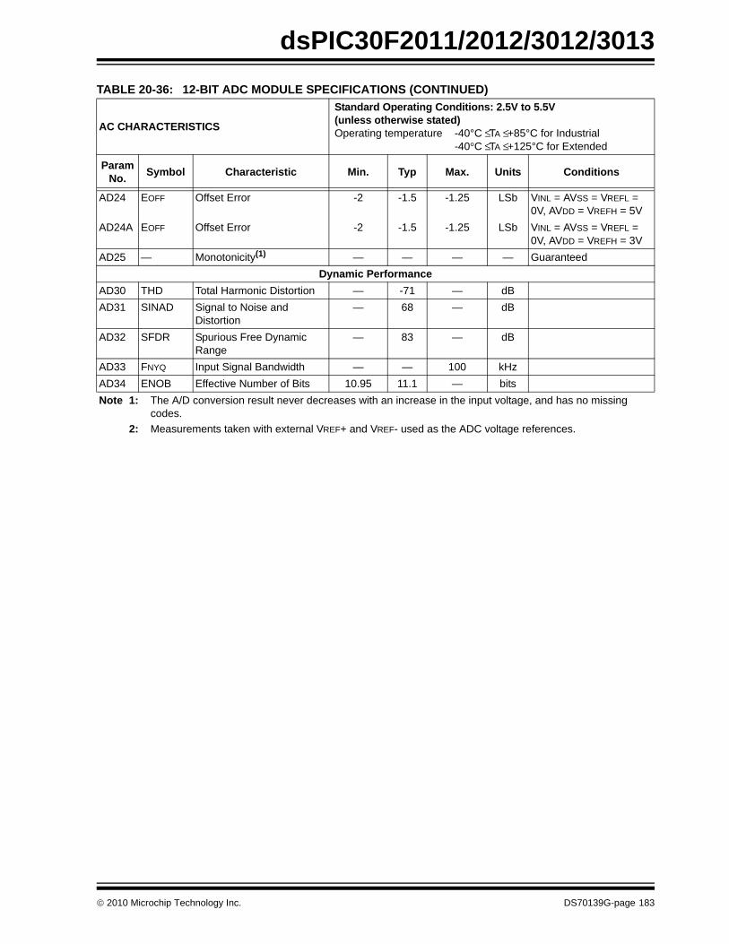
dsPIC30F2011/2012/3012/3013
AD24 EOFF Offset Error -2 -1.5 -1.25 LSb VINL = AVSS = VREFL = 0V, AVDD = VREFH = 5V
AD24A EOFF Offset Error -2 -1.5 -1.25 LSb VINL = AVSS = VREFL = 0V, AVDD = VREFH = 3V
AD25 — Monotonicity(1) — — — — GuaranteedDynamic Performance
AD30 THD Total Harmonic Distortion — -71 — dBAD31 SINAD Signal to Noise and
Distortion — 68 — dB
AD32 SFDR Spurious Free DynamicRange
— 83 — dB
AD33 FNYQ Input Signal Bandwidth — — 100 kHzAD34 ENOB Effective Number of Bits 10.95 11.1 — bits
TABLE 20-36: 12-BIT ADC MODULE SPECIFICATIONS (CONTINUED)
AC CHARACTERISTICS
Standard Operating Conditions: 2.5V to 5.5V(unless otherwise stated)Operating temperature -40°C ≤ TA ≤ +85°C for Industrial
-40°C ≤ TA ≤ +125°C for Extended
Param No. Symbol Characteristic Min. Typ Max. Units Conditions
Note 1: The A/D conversion result never decreases with an increase in the input voltage, and has no missing codes.
2: Measurements taken with external VREF+ and VREF- used as the ADC voltage references.
© 2010 Microchip Technology Inc. DS70139G-page 183
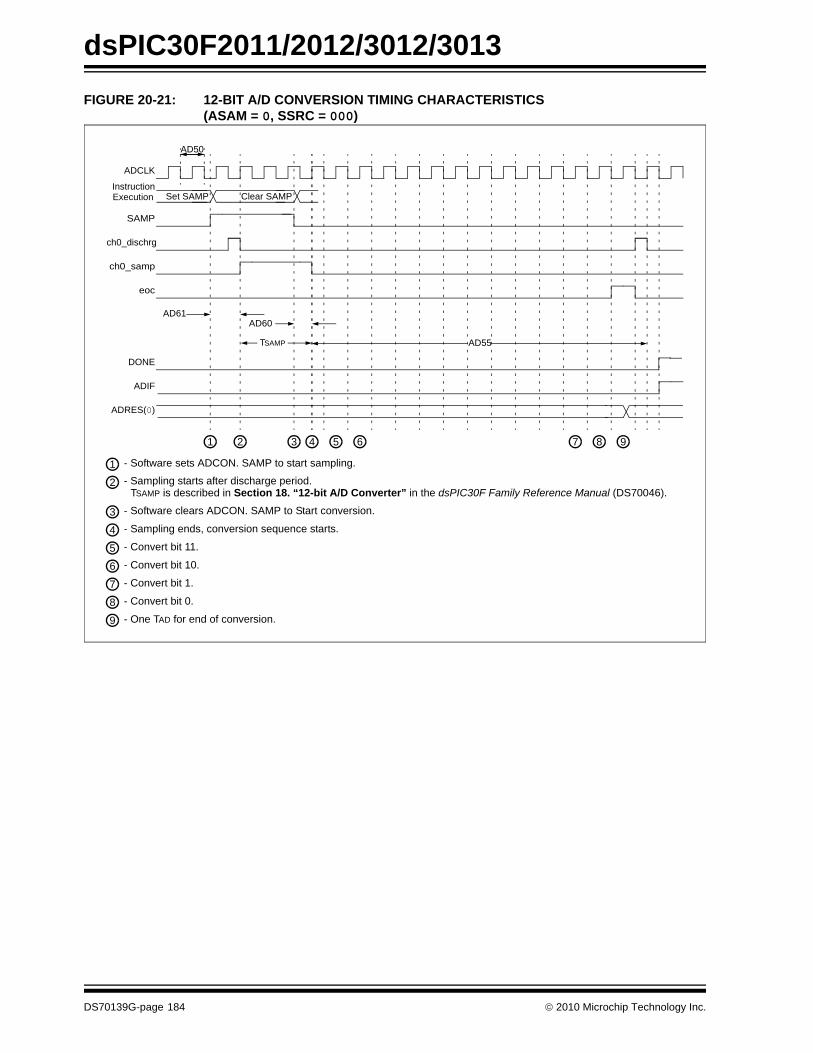
dsPIC30F2011/2012/3012/3013
FIGURE 20-21: 12-BIT A/D CONVERSION TIMING CHARACTERISTICS(ASAM = 0, SSRC = 000)
AD55TSAMP
Clear SAMPSet SAMP
AD61
ADCLK
Instruction
SAMP
ch0_dischrg
ch0_samp
AD60
DONE
ADIF
ADRES(0)
1 2 3 4 5 6 87
1 - Software sets ADCON. SAMP to start sampling.
2 - Sampling starts after discharge period.
3 - Software clears ADCON. SAMP to Start conversion.
4 - Sampling ends, conversion sequence starts.
5 - Convert bit 11.
9 - One TAD for end of conversion.
AD50
eoc
9
6 - Convert bit 10.
7 - Convert bit 1.
8 - Convert bit 0.
Execution
TSAMP is described in Section 18. “12-bit A/D Converter” in the dsPIC30F Family Reference Manual (DS70046).
DS70139G-page 184 © 2010 Microchip Technology Inc.
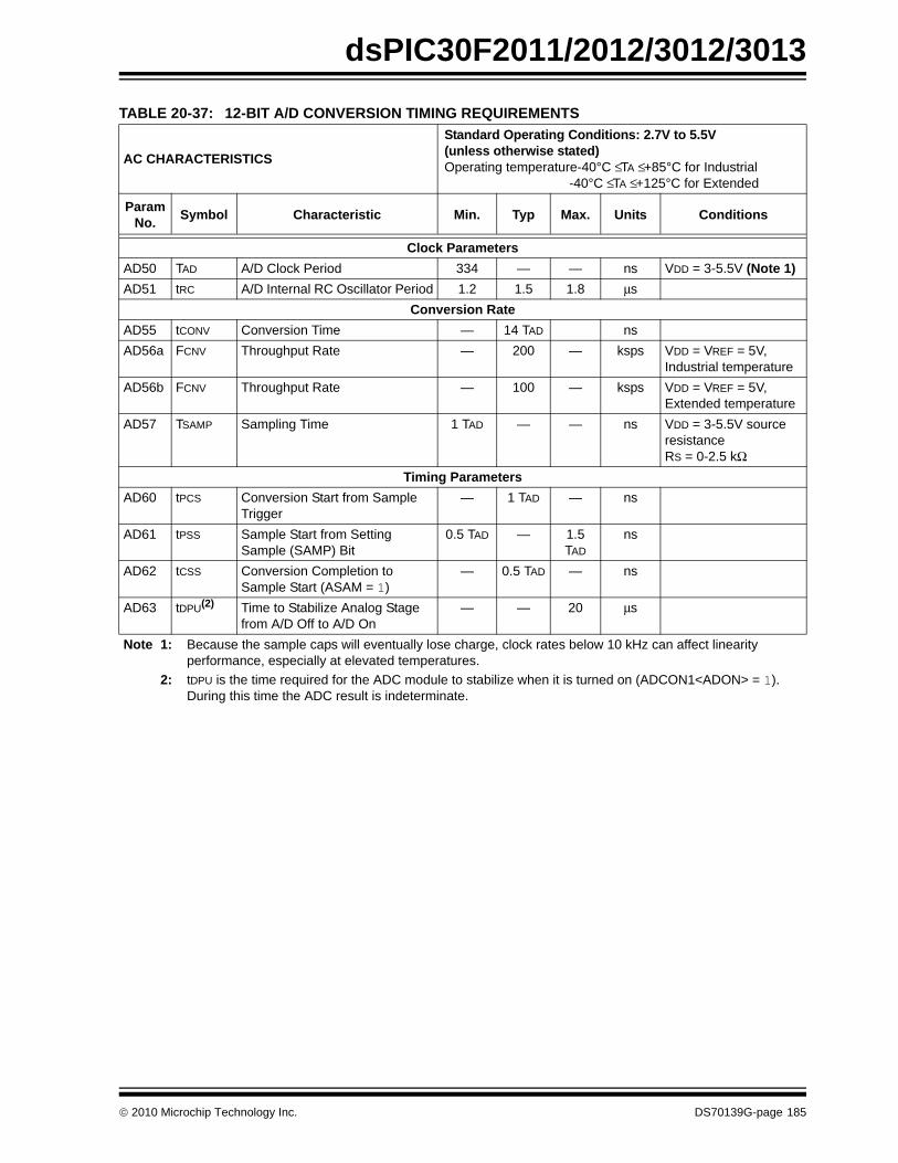
dsPIC30F2011/2012/3012/3013
TABLE 20-37: 12-BIT A/D CONVERSION TIMING REQUIREMENTS
AC CHARACTERISTICS
Standard Operating Conditions: 2.7V to 5.5V(unless otherwise stated)Operating temperature-40°C ≤ TA ≤ +85°C for Industrial
-40°C ≤ TA ≤ +125°C for Extended
Param No. Symbol Characteristic Min. Typ Max. Units Conditions
Clock ParametersAD50 TAD A/D Clock Period 334 — — ns VDD = 3-5.5V (Note 1)AD51 tRC A/D Internal RC Oscillator Period 1.2 1.5 1.8 μs
Conversion RateAD55 tCONV Conversion Time — 14 TAD nsAD56a FCNV Throughput Rate — 200 — ksps VDD = VREF = 5V,
Industrial temperatureAD56b FCNV Throughput Rate — 100 — ksps VDD = VREF = 5V,
Extended temperatureAD57 TSAMP Sampling Time 1 TAD — — ns VDD = 3-5.5V source
resistanceRS = 0-2.5 kΩ
Timing ParametersAD60 tPCS Conversion Start from Sample
Trigger— 1 TAD — ns
AD61 tPSS Sample Start from SettingSample (SAMP) Bit
0.5 TAD — 1.5 TAD
ns
AD62 tCSS Conversion Completion toSample Start (ASAM = 1)
— 0.5 TAD — ns
AD63 tDPU(2) Time to Stabilize Analog Stagefrom A/D Off to A/D On
— — 20 μs
Note 1: Because the sample caps will eventually lose charge, clock rates below 10 kHz can affect linearity performance, especially at elevated temperatures.
2: tDPU is the time required for the ADC module to stabilize when it is turned on (ADCON1<ADON> = 1). During this time the ADC result is indeterminate.
© 2010 Microchip Technology Inc. DS70139G-page 185

dsPIC30F2011/2012/3012/3013
NOTES:DS70139G-page 186 © 2010 Microchip Technology Inc.
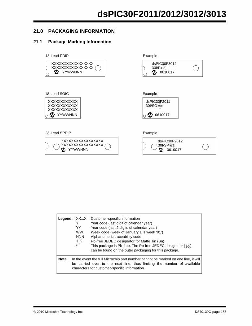
dsPIC30F2011/2012/3012/3013
21.0 PACKAGING INFORMATION
21.1 Package Marking Information
XXXXXXXXXXXXXXXXXYYWWNNN
28-Lead SPDIP Example
XXXXXXXXXXXXXXXXX
18-Lead PDIP Example
XXXXXXXXXXXXXXXXXXXXXXXXXXXXXXXXXX
YYWWNNN
dsPIC30F3012
0610017
Legend: XX...X Customer-specific informationY Year code (last digit of calendar year)YY Year code (last 2 digits of calendar year)WW Week code (week of January 1 is week ‘01’)NNN Alphanumeric traceability code Pb-free JEDEC designator for Matte Tin (Sn)* This package is Pb-free. The Pb-free JEDEC designator ( )
can be found on the outer packaging for this package.
Note: In the event the full Microchip part number cannot be marked on one line, it willbe carried over to the next line, thus limiting the number of availablecharacters for customer-specific information.
3e
3e
dsPIC30F2012
061001730I/SP 3e
30I/P 3e
18-Lead SOIC Example
YYWWNNNXXXXXXXXXXXXXXXXXXXXXXXXXXXXXXXXXXXX
0610017
30I/SOdsPIC30F2011
3e
© 2010 Microchip Technology Inc. DS70139G-page 187
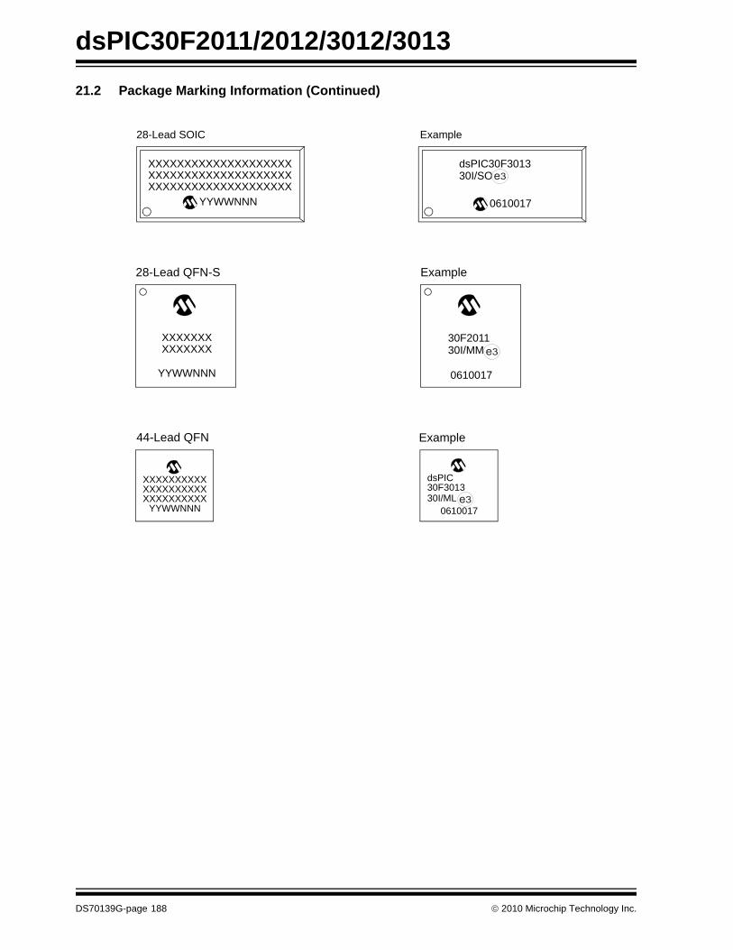
dsPIC30F2011/2012/3012/3013
21.2 Package Marking Information (Continued)30F2011
28-Lead SOIC
XXXXXXXXXXXXXXXXXXXXXXXXXXXXXXXXXXXXXXXXXXXXXXXXXXXXXXXXXXXX
YYWWNNN
Example
dsPIC30F3013
0610017
XXXXXXXXXXXXXXXXXXXXXXXXXXXXXX
YYWWNNN
44-Lead QFN
dsPIC 30F3013
0610017
30I/SO 3e
30I/ML 3e
28-Lead QFN-S
XXXXXXXXXXXXXX
YYWWNNN
Example
30I/MM
0610017
Example
3e
DS70139G-page 188 © 2010 Microchip Technology Inc.
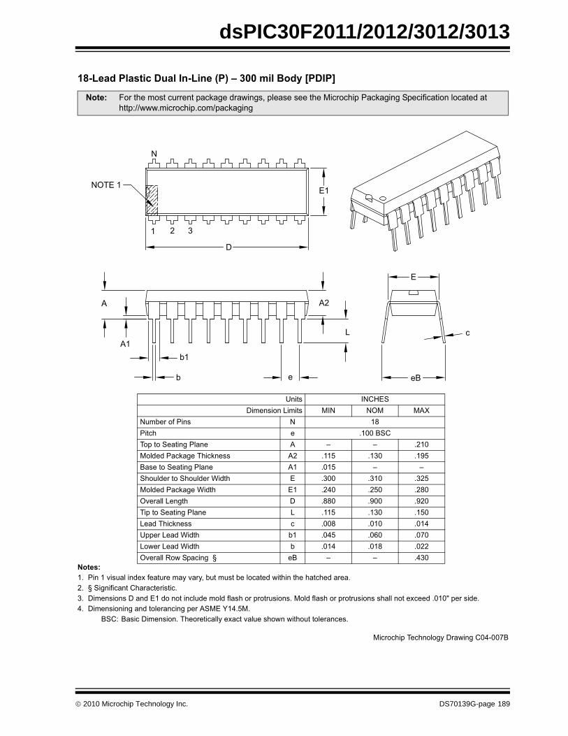
dsPIC30F2011/2012/3012/3013
���������� ������������������������������
�
�� �� �� ������ �!"�����#�$�%��&"��'��� ��(�)"&�'"!&�)�����&�#�*�&����&�����&���#������� +������%����&�,����&��!&���-� ��'��!��!�����#�.��#��&�����"#��'�#�%��!����&"!��!����#�%��!����&"!��!�!������&��$���#�����/����!�#���� ��'��!��������#�&���������������.�0������
1�,2 1�!�����'��!���� ���&��������$��&� ��"��!�*��*�&�"&�&������!�
�� � 3�&���'!&��"��&����4����#�*���!(�����!��!���&��������������4�����������%���&������&�#��&��&&�255***�'��������'5���4�����
6��&! �7,8.���'��!���9�'�&! ��7 7:� ��;
7"')��%����! 7 �<��&�� � �����1�, ��&����&��������� � = = ������#�#����4���� ���4��!! �� ���� ��-� ����1�!��&����&��������� �� ���� = =��"�#��&���"�#��>�#&� . �-�� �-�� �-����#�#����4����>�#&� .� ���� ���� ��<�: �����9���&� � �<<� ���� ���� ���&����&��������� 9 ���� ��-� ����9��#� ���4��!! � ���< ���� ����6����9��#�>�#&� )� ���� ��?� ����9*��9��#�>�#&� ) ���� ���< ����: ������*����������+ �1 = = ��-�
NOTE 1
N
E1
D
1 2 3
A
A1
A2
L
E
eB
c
e
b1
b
������� ������� ��*��� ,������1
© 2010 Microchip Technology Inc. DS70139G-page 189
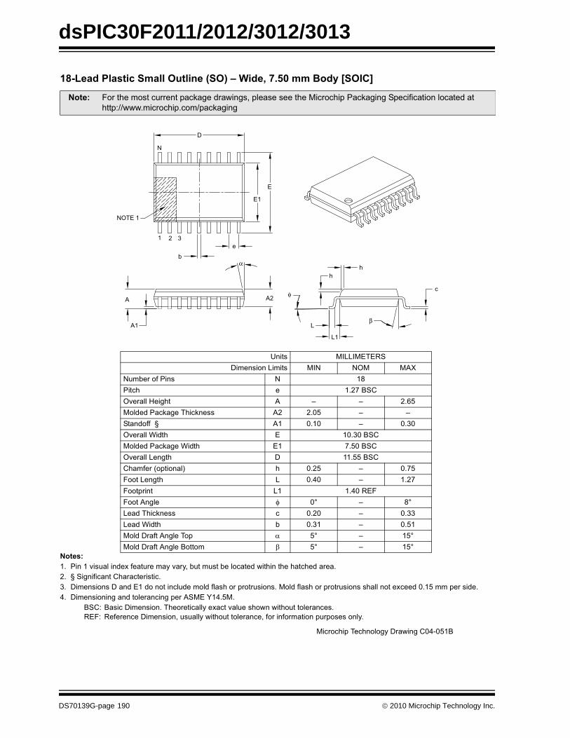
dsPIC30F2011/2012/3012/3013
���������� ��!����"� �����!"��#���$%&'��������!"�(�
�� �� �� ������ �!"�����#�$�%��&"��'��� ��(�)"&�'"!&�)�����&�#�*�&����&�����&���#������� +������%����&�,����&��!&���-� ��'��!��!�����#�.��#��&�����"#��'�#�%��!����&"!��!����#�%��!����&"!��!�!������&��$���#������''����!�#���� ��'��!��������#�&���������������.�0������
1�,2 1�!�����'��!���� ���&��������$��&� ��"��!�*��*�&�"&�&������!��.32 ��%��������'��!��(�"!"�����*�&�"&�&������(�%���%'�&����"�!�!�����
�� � 3�&���'!&��"��&����4����#�*���!(�����!��!���&��������������4�����������%���&������&�#��&��&&�255***�'��������'5���4�����
6��&! ��99��. .����'��!���9�'�&! ��7 7:� ��;
7"')��%����! 7 �<��&�� � �����1�,: �����8����& � = = ��?���#�#����4���� ���4��!! �� ���� = =�&��#%%��+ �� ���� = ��-�: �����>�#&� . ���-��1�,��#�#����4����>�#&� .� �����1�,: �����9���&� � ������1�,,��'%��@�&����A � ���� = ����3&�9���&� 9 ���� = ����3&���& 9� ������.33&������ � �B = <B9��#� ���4��!! � ���� = ��--9��#�>�#&� ) ��-� = ������#���%&������� � � �B = ��B��#���%&�������1&&' � �B = ��B
NOTE 1
D
N
E
E1
e
b
1 2 3
A
A1
A2
L
L1
h
h
c
β
φ
α
������� ������� ��*��� ,������1
DS70139G-page 190 © 2010 Microchip Technology Inc.
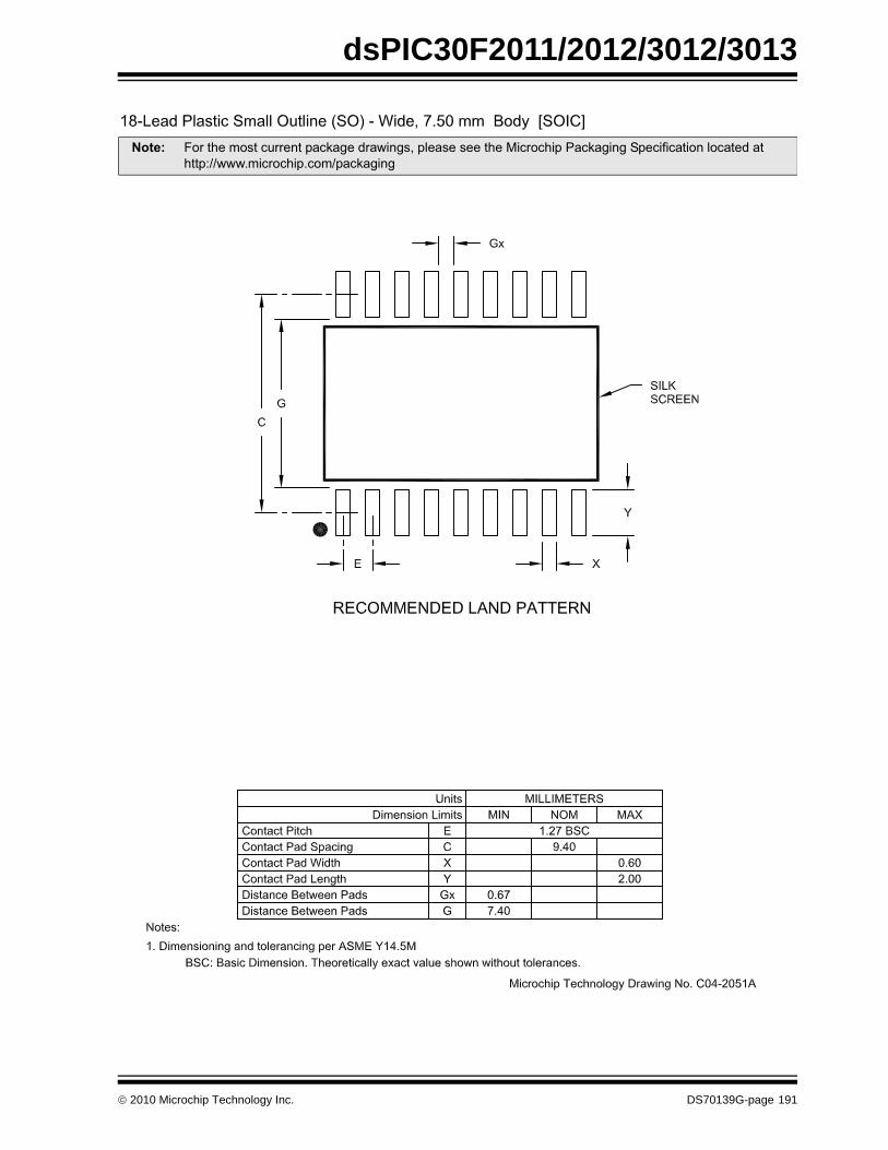
dsPIC30F2011/2012/3012/3013
Note: For the most current package drawings, please see the Microchip Packaging Specification located at
http://www.microchip.com/packaging
© 2010 Microchip Technology Inc. DS70139G-page 191
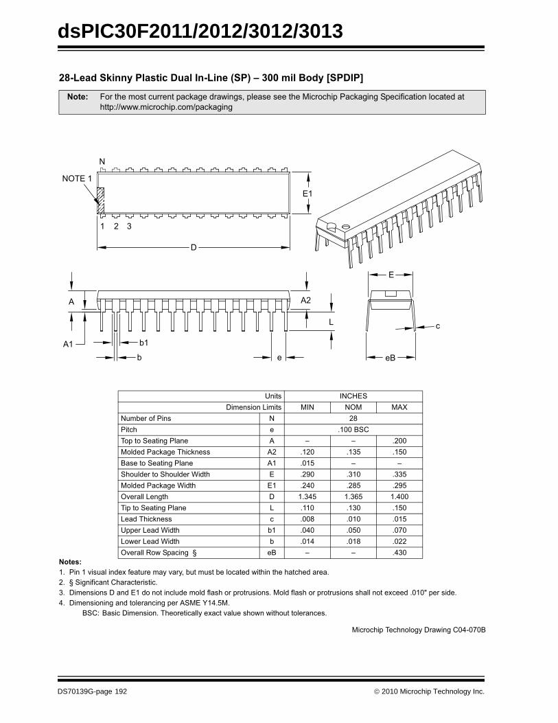
dsPIC30F2011/2012/3012/3013
)������!*������� ��������������!�������������!���
�� �� �� ������ �!"�����#�$�%��&"��'��� ��(�)"&�'"!&�)�����&�#�*�&����&�����&���#������� +������%����&�,����&��!&���-� ��'��!��!�����#�.��#��&�����"#��'�#�%��!����&"!��!����#�%��!����&"!��!�!������&��$���#�����/����!�#���� ��'��!��������#�&���������������.�0������
1�,2 1�!�����'��!���� ���&��������$��&� ��"��!�*��*�&�"&�&������!�
�� � 3�&���'!&��"��&����4����#�*���!(�����!��!���&��������������4�����������%���&������&�#��&��&&�255***�'��������'5���4�����
6��&! �7,8.���'��!���9�'�&! ��7 7:� ��;
7"')��%����! 7 �<��&�� � �����1�, ��&����&��������� � = = ������#�#����4���� ���4��!! �� ���� ��-� ����1�!��&����&��������� �� ���� = =��"�#��&���"�#��>�#&� . ���� �-�� �--���#�#����4����>�#&� .� ���� ��<� ����: �����9���&� � ��-�� ��-?� ����� ���&����&��������� 9 ���� ��-� ����9��#� ���4��!! � ���< ���� ����6����9��#�>�#&� )� ���� ���� ����9*��9��#�>�#&� ) ���� ���< ����: ������*����������+ �1 = = ��-�
NOTE 1
N
1 2
D
E1
eB
c
E
L
A2
eb
b1A1
A
3
������� ������� ��*��� ,������1
DS70139G-page 192 © 2010 Microchip Technology Inc.
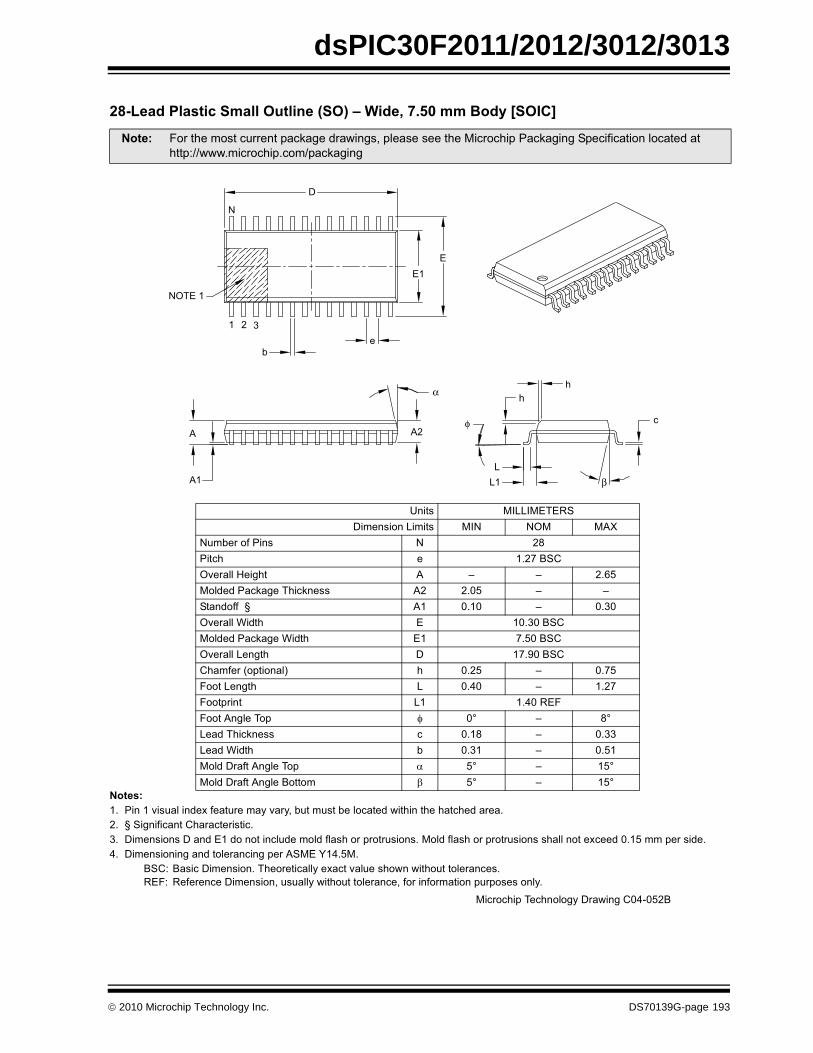
dsPIC30F2011/2012/3012/3013
)��������� ��!����"� �����!"��#���$%&'��������!"�(�
�� �� �� ������ �!"�����#�$�%��&"��'��� ��(�)"&�'"!&�)�����&�#�*�&����&�����&���#������� +������%����&�,����&��!&���-� ��'��!��!�����#�.��#��&�����"#��'�#�%��!����&"!��!����#�%��!����&"!��!�!������&��$���#������''����!�#���� ��'��!��������#�&���������������.�0������
1�,2 1�!�����'��!���� ���&��������$��&� ��"��!�*��*�&�"&�&������!��.32 ��%��������'��!��(�"!"�����*�&�"&�&������(�%���%'�&����"�!�!�����
�� � 3�&���'!&��"��&����4����#�*���!(�����!��!���&��������������4�����������%���&������&�#��&��&&�255***�'��������'5���4�����
6��&! ��99��. .����'��!���9�'�&! ��7 7:� ��;
7"')��%����! 7 �<��&�� � �����1�,: �����8����& � = = ��?���#�#����4���� ���4��!! �� ���� = =�&��#%%��+ �� ���� = ��-�: �����>�#&� . ���-��1�,��#�#����4����>�#&� .� �����1�,: �����9���&� � ������1�,,��'%��@�&����A � ���� = ����3&�9���&� 9 ���� = ����3&���& 9� ������.33&������� � � �B = <B9��#� ���4��!! � ���< = ��--9��#�>�#&� ) ��-� = ������#���%&������� � � �B = ��B��#���%&�������1&&' � �B = ��B
c
h
h
L
L1
A2
A1
A
NOTE 1
1 2 3
b
e
E
E1
D
φ
β
α
N
������� ������� ��*��� ,������1
© 2010 Microchip Technology Inc. DS70139G-page 193
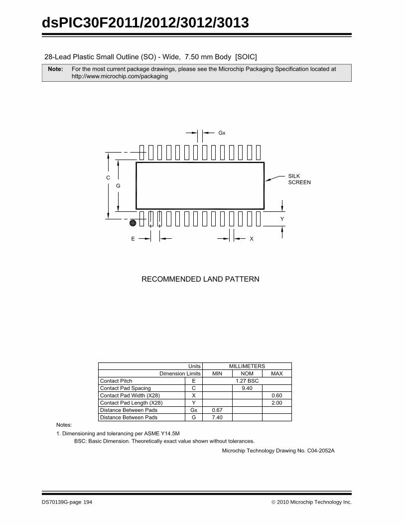
dsPIC30F2011/2012/3012/3013
Note: For the most current package drawings, please see the Microchip Packaging Specification located at
http://www.microchip.com/packaging
DS70139G-page 194 © 2010 Microchip Technology Inc.
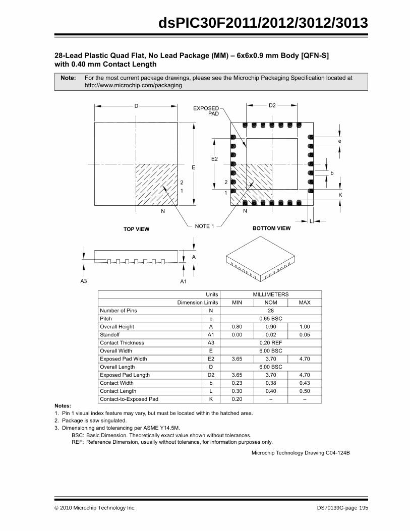
dsPIC30F2011/2012/3012/3013
)��������� ��+���,�� $��������*�-��..��/0/0�&1�������+,��!�2� 3�&4���(�� �� ���- 3
�� �� �� ������ �!"�����#�$�%��&"��'��� ��(�)"&�'"!&�)�����&�#�*�&����&�����&���#������� ���4�����!�!�*�!���"��&�#�-� ��'��!��������#�&���������������.�0������
1�,2 1�!�����'��!���� ���&��������$��&� ��"��!�*��*�&�"&�&������!��.32 ��%��������'��!��(�"!"�����*�&�"&�&������(�%���%'�&����"�!�!�����
�� � 3�&���'!&��"��&����4����#�*���!(�����!��!���&��������������4�����������%���&������&�#��&��&&�255***�'��������'5���4�����
6��&! ��99��. .����'��!���9�'�&! ��7 7:� ��;
7"')��%����! 7 �<��&�� � ��?��1�,: �����8����& � ��<� ���� �����&��#%%� �� ���� ���� ����,�&��&� ���4��!! �- ������.3: �����>�#&� . ?����1�,.$�!�#���#�>�#&� .� -�?� -��� ����: �����9���&� � ?����1�,.$�!�#���#�9���&� �� -�?� -��� ����,�&��&�>�#&� ) ���- ��-< ���-,�&��&�9���&� 9 ��-� ���� ����,�&��&�&�.$�!�#���# C ���� = =
D
E
2
1
N
E2
EXPOSEDPAD
2
1
D2
N
e
b
K
LNOTE 1
A3
A
A1
TOP VIEW BOTTOM VIEW
������� ������� ��*��� ,������1
© 2010 Microchip Technology Inc. DS70139G-page 195
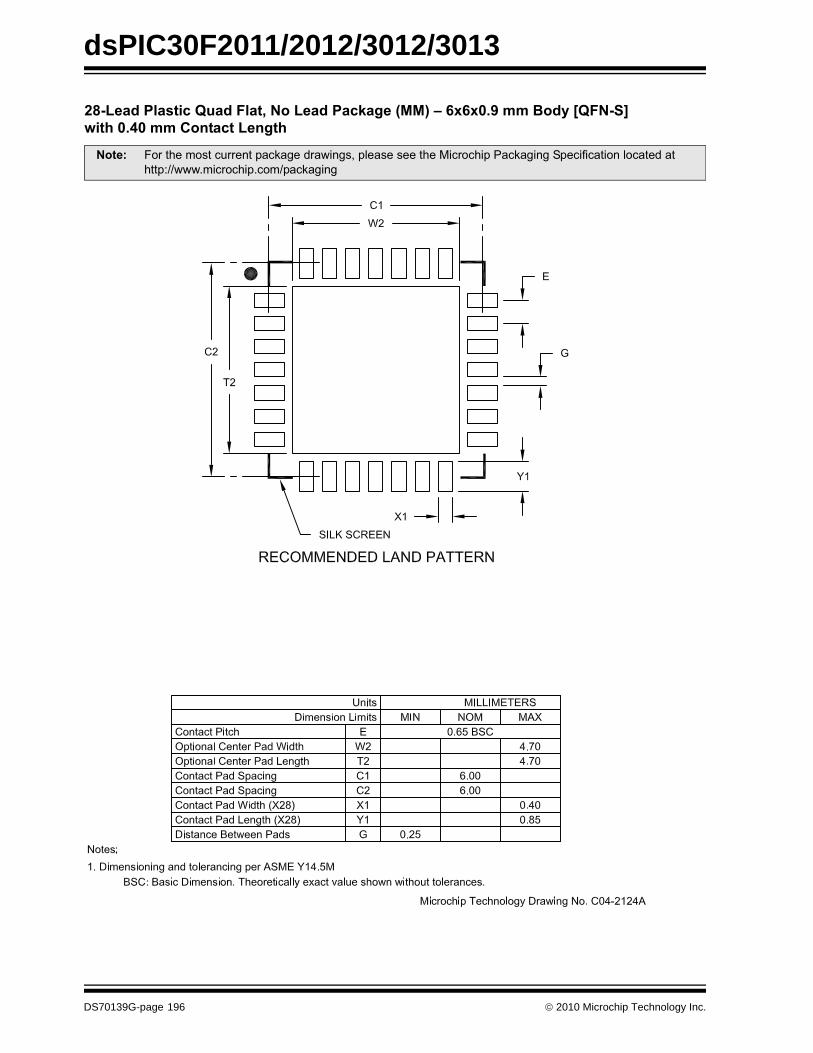
dsPIC30F2011/2012/3012/3013
)��������� ��+���,�� $��������*�-��..��/0/0�&1�������+,��!�2� 3�&4���(�� �� ���- 3
�� � 3�&���'!&��"��&����4����#�*���!(�����!��!���&��������������4�����������%���&������&�#��&��&&�255***�'��������'5���4�����
DS70139G-page 196 © 2010 Microchip Technology Inc.
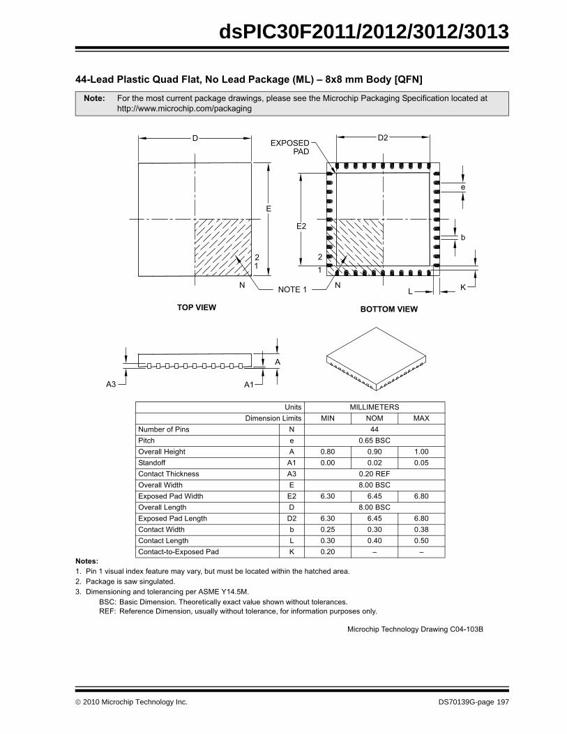
dsPIC30F2011/2012/3012/3013
44�������� ��+���,�� $��������*�-��.����0��������+,��
�� �� �� ������ �!"�����#�$�%��&"��'��� ��(�)"&�'"!&�)�����&�#�*�&����&�����&���#������� ���4�����!�!�*�!���"��&�#�-� ��'��!��������#�&���������������.�0������
1�,2 1�!�����'��!���� ���&��������$��&� ��"��!�*��*�&�"&�&������!��.32 ��%��������'��!��(�"!"�����*�&�"&�&������(�%���%'�&����"�!�!�����
�� � 3�&���'!&��"��&����4����#�*���!(�����!��!���&��������������4�����������%���&������&�#��&��&&�255***�'��������'5���4�����
6��&! ��99��. .����'��!���9�'�&! ��7 7:� ��;
7"')��%����! 7 ����&�� � ��?��1�,: �����8����& � ��<� ���� �����&��#%%� �� ���� ���� ����,�&��&� ���4��!! �- ������.3: �����>�#&� . <����1�,.$�!�#���#�>�#&� .� ?�-� ?��� ?�<�: �����9���&� � <����1�,.$�!�#���#�9���&� �� ?�-� ?��� ?�<�,�&��&�>�#&� ) ���� ��-� ��-<,�&��&�9���&� 9 ��-� ���� ����,�&��&�&�.$�!�#���# C ���� = =
DEXPOSED
PAD
D2
e
b
KL
E2
2
1
NNOTE 1
21
E
N
BOTTOM VIEWTOP VIEW
A3 A1
A
������� ������� ��*��� ,�����-1
© 2010 Microchip Technology Inc. DS70139G-page 197
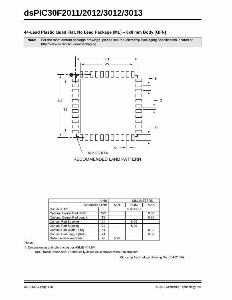
dsPIC30F2011/2012/3012/3013
44�������� ��+���,�� $��������*�-��.����0��������+,��
�� � 3�&���'!&��"��&����4����#�*���!(�����!��!���&��������������4�����������%���&������&�#��&��&&�255***�'��������'5���4�����
DS70139G-page 198 © 2010 Microchip Technology Inc.
dsPIC30F2011/2012/3012/3013
APPENDIX A: REVISION HISTORY
Revision D (August 2006)Previous versions of this data sheet containedAdvance or Preliminary Information. They weredistributed with incomplete characterization data.
This revision reflects these updates:
• Supported I2C Slave Addresses (see Table 14-1)
• ADC Conversion Clock selection to allow 200 kHz sampling rate (see Section 16.0 “12-bit Analog-to-Digital Converter (ADC) Module”)
• Operating Current (IDD) Specifications (see Table 20-5)
• Idle Current (IIDLE) Specifications(see Table 20-6)
• Power-Down Current (IPD) Specifications(see Table 20-7)
• I/O pin Input Specifications (see Table 20-8)
• BOR voltage limits (see Table 20-11)
• Watchdog Timer time-out limits (see Table 20-21)
Revision E (December 2006)This revision includes updates to the packaging diagrams.
Revision F (May 2008)This revision reflects these updates:
• Added FUSE Configuration Register (FICD) details (see Section 17.7 “Device Configuration Registers” and Table 17-8)
• Added Note 2 to Device Configuration Registers table (Table 17-8)
• Updated Bit 10 in the UART2 Register Map (see Table 15-2). This bit is unimplemented.
• Electrical Specifications:- Resolved TBD values for parameters DO10,
DO16, DO20, and DO26 (see Table 20-9)- 10-bit High-Speed ADC tPDU timing
parameter (time to stabilize) has been updated from 20 µs typical to 20 µs maximum (see Table 20-37)
- Parameter OS65 (Internal RC Accuracy) has been expanded to reflect multiple Min and Max values for different temperatures (see Table 20-19)
- Parameter DC12 (RAM Data Retention Voltage) has been updated to include a Min value (see Table 20-4)
- Parameter D134 (Erase/Write Cycle Time) has been updated to include Min and Max values and the Typ value has been removed (see Table 20-12)
- Removed parameters OS62 (Internal FRC Jitter) and OS64 (Internal FRC Drift) and Note 2 from AC Characteristics (see Table 20-18)
- Parameter OS63 (Internal FRC Accuracy) has been expanded to reflect multiple Min and Max values for different temperatures (see Table 20-18)
- Updated Min and Max values and Conditions for parameter SY11 and updated Min, Typ, and Max values and Conditions for parameter SY20 (see Table 20-21)
• Additional minor corrections throughout the document
© 2010 Microchip Technology Inc. DS70139G-page 199
dsPIC30F2011/2012/3012/3013
Revision G (November 2010)This revision includes minor typographical andformatting changes throughout the data sheet text.The major changes are referenced by their respectivesection in Table A-1.
TABLE A-1: MAJOR SECTION UPDATESSection Name Update Description
“High-Performance, 16-Bit Digital Signal Controllers”
Added Note 1 to all QFN pin diagrams (see “Pin Diagrams”).
Section 1.0 “Device Overview” Updated the Pinout I/O Descriptions for AVDD and AVSS (see Table 1-1).Section 17.0 “System Integration” Added a shaded note on OSCTUN functionality in Section 17.2.5 “Fast RC
Oscillator (FRC)”.Section 20.0 “Electrical Characteristics”
Updated the maximum value for parameter DI19 and the minimum value for parameter DI29 in the I/O Pin Input Specifications (see Table 20-8).
Removed parameter D136 and updated the minimum, typical, maximum, and conditions for parameters D122 and D134 in the Program and EEPROM specifications (see Table 20-12).
Renamed parameter AD56 to AD56a and added parameter AD56b to the 12-bit A/D Conversion Timing Requirements (see Table 20-37).
“Product Identification System” Added the “MM” package definition.
DS70139G-page 200 © 2010 Microchip Technology Inc.
dsPIC30F2011/2012/3012/3013
INDEXNumerics12-bit Analog-to-Digital Converter (A/D) Module .............. 113
AA/D .................................................................................... 113
Aborting a Conversion .............................................. 115ADCHS Register ....................................................... 113ADCON1 Register..................................................... 113ADCON2 Register..................................................... 113ADCON3 Register..................................................... 113ADCSSL Register ..................................................... 113ADPCFG Register..................................................... 113Configuring Analog Port Pins.............................. 60, 119Connection Considerations....................................... 119Conversion Operation ............................................... 114Effects of a Reset...................................................... 118Operation During CPU Idle Mode ............................. 118Operation During CPU Sleep Mode.......................... 118Output Formats ......................................................... 118Power-Down Modes.................................................. 118Programming the Sample Trigger............................. 115Register Map............................................................. 121Result Buffer ............................................................. 114Sampling Requirements............................................ 117Selecting the Conversion Sequence......................... 114
AC Characteristics ............................................................ 160Load Conditions ........................................................ 160
AC Temperature and Voltage Specifications .................... 160ADC
Selecting the Conversion Clock ................................ 115ADC Conversion Speeds .................................................. 116Address Generator Units .................................................... 43Alternate Vector Table ........................................................ 69Analog-to-Digital Converter. See ADC.Assembler
MPASM Assembler................................................... 146Automatic Clock Stretch.................................................... 100
During 10-bit Addressing (STREN = 1)..................... 100During 7-bit Addressing (STREN = 1)....................... 100Receive Mode ........................................................... 100Transmit Mode .......................................................... 100
BBandgap Start-up Time
Requirements............................................................ 166Timing Characteristics .............................................. 166
Barrel Shifter ....................................................................... 27Bit-Reversed Addressing .................................................... 46
Example ...................................................................... 47Implementation ........................................................... 46Modifier Values Table ................................................. 47Sequence Table (16-Entry)......................................... 47
Block Diagrams12-bit ADC Functional............................................... 11316-bit Timer1 Module .................................................. 7316-bit Timer2............................................................... 7916-bit Timer3............................................................... 7932-bit Timer2/3............................................................ 78DSP Engine ................................................................ 24dsPIC30F2011 ............................................................ 12dsPIC30F2012 ............................................................ 13dsPIC30F3013 ............................................................ 15External Power-on Reset Circuit............................... 131
I2C .............................................................................. 98Input Capture Mode.................................................... 83Oscillator System...................................................... 125Output Compare Mode ............................................... 87Reset System ........................................................... 129Shared Port Structure................................................. 59SPI.............................................................................. 94SPI Master/Slave Connection..................................... 95UART Receiver......................................................... 106UART Transmitter..................................................... 105
BOR Characteristics ......................................................... 158BOR. See Brown-out Reset.Brown-out Reset
Characteristics.......................................................... 158Timing Requirements ............................................... 165
CC Compilers
MPLAB C18.............................................................. 146CAN Module
I/O Timing Characteristics ........................................ 181I/O Timing Requirements.......................................... 181
CLKOUT and I/O TimingCharacteristics.......................................................... 164Requirements ........................................................... 164
Code ExamplesData EEPROM Block Erase ....................................... 56Data EEPROM Block Write ........................................ 58Data EEPROM Read.................................................. 55Data EEPROM Word Erase ....................................... 56Data EEPROM Word Write ........................................ 57Erasing a Row of Program Memory ........................... 51Initiating a Programming Sequence ........................... 52Loading Write Latches................................................ 52
Code Protection................................................................ 123Control Registers ................................................................ 50
NVMADR .................................................................... 50NVMADRU ................................................................. 50NVMCON.................................................................... 50NVMKEY .................................................................... 50
Core ArchitectureOverview..................................................................... 19
CPU Architecture Overview................................................ 19Customer Change Notification Service............................. 205Customer Notification Service .......................................... 205Customer Support............................................................. 205
DData Accumulators and Adder/Subtractor .......................... 25
Data Space Write Saturation ...................................... 27Overflow and Saturation ............................................. 25Round Logic ............................................................... 26Write-Back .................................................................. 26
Data Address Space........................................................... 35Alignment.................................................................... 38Alignment (Figure) ...................................................... 38Effect of Invalid Memory Accesses (Table) ................ 38MCU and DSP (MAC Class) Instructions Example .... 37Memory Map......................................................... 35, 36Near Data Space ........................................................ 39Software Stack ........................................................... 39Spaces........................................................................ 38Width .......................................................................... 38
Data EEPROM Memory...................................................... 55Erasing ....................................................................... 56Erasing, Block............................................................. 56
© 2010 Microchip Technology Inc. DS70139G-page 201
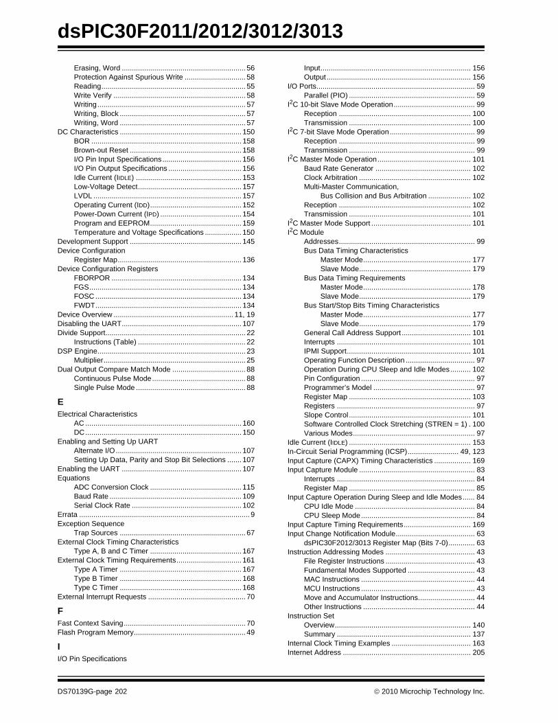
dsPIC30F2011/2012/3012/3013
Erasing, Word ............................................................. 56Protection Against Spurious Write .............................. 58Reading....................................................................... 55Write Verify ................................................................. 58Writing......................................................................... 57Writing, Block .............................................................. 57Writing, Word .............................................................. 57DC Characteristics ............................................................ 150BOR .......................................................................... 158Brown-out Reset ....................................................... 158I/O Pin Input Specifications....................................... 156I/O Pin Output Specifications .................................... 156Idle Current (IIDLE) .................................................... 153Low-Voltage Detect................................................... 157LVDL ......................................................................... 157Operating Current (IDD)............................................. 152Power-Down Current (IPD) ........................................ 154Program and EEPROM............................................. 159Temperature and Voltage Specifications .................. 150
Development Support ....................................................... 145Device Configuration
Register Map............................................................. 136Device Configuration Registers
FBORPOR ................................................................ 134FGS........................................................................... 134FOSC ........................................................................ 134FWDT........................................................................ 134
Device Overview ........................................................... 11, 19Disabling the UART........................................................... 107Divide Support..................................................................... 22
Instructions (Table) ..................................................... 22DSP Engine......................................................................... 23
Multiplier...................................................................... 25Dual Output Compare Match Mode .................................... 88
Continuous Pulse Mode.............................................. 88Single Pulse Mode ...................................................... 88
EElectrical Characteristics
AC ............................................................................. 160DC............................................................................. 150
Enabling and Setting Up UARTAlternate I/O.............................................................. 107Setting Up Data, Parity and Stop Bit Selections ....... 107
Enabling the UART ........................................................... 107Equations
ADC Conversion Clock ............................................. 115Baud Rate ................................................................. 109Serial Clock Rate ...................................................... 102
Errata .................................................................................... 9Exception Sequence
Trap Sources .............................................................. 67External Clock Timing Characteristics
Type A, B and C Timer ............................................. 167External Clock Timing Requirements................................ 161
Type A Timer ............................................................ 167Type B Timer ............................................................ 168Type C Timer ............................................................ 168
External Interrupt Requests ................................................ 70
FFast Context Saving............................................................ 70Flash Program Memory....................................................... 49
II/O Pin Specifications
Input.......................................................................... 156Output ....................................................................... 156
I/O Ports.............................................................................. 59Parallel (PIO) .............................................................. 59
I2C 10-bit Slave Mode Operation........................................ 99Reception ................................................................. 100Transmission ............................................................ 100
I2C 7-bit Slave Mode Operation.......................................... 99Reception ................................................................... 99Transmission .............................................................. 99
I2C Master Mode Operation.............................................. 101Baud Rate Generator ............................................... 102Clock Arbitration ....................................................... 102Multi-Master Communication,
Bus Collision and Bus Arbitration ..................... 102Reception ................................................................. 102Transmission ............................................................ 101
I2C Master Mode Support ................................................. 101I2C Module
Addresses................................................................... 99Bus Data Timing Characteristics
Master Mode..................................................... 177Slave Mode....................................................... 179
Bus Data Timing RequirementsMaster Mode..................................................... 178Slave Mode....................................................... 179
Bus Start/Stop Bits Timing CharacteristicsMaster Mode..................................................... 177Slave Mode....................................................... 179
General Call Address Support .................................. 101Interrupts .................................................................. 101IPMI Support............................................................. 101Operating Function Description .................................. 97Operation During CPU Sleep and Idle Modes.......... 102Pin Configuration ........................................................ 97Programmer’s Model .................................................. 97Register Map ............................................................ 103Registers .................................................................... 97Slope Control ............................................................ 101Software Controlled Clock Stretching (STREN = 1) . 100Various Modes............................................................ 97
Idle Current (IIDLE) ............................................................ 153In-Circuit Serial Programming (ICSP)......................... 49, 123Input Capture (CAPX) Timing Characteristics .................. 169Input Capture Module ......................................................... 83
Interrupts .................................................................... 84Register Map .............................................................. 85
Input Capture Operation During Sleep and Idle Modes...... 84CPU Idle Mode ........................................................... 84CPU Sleep Mode........................................................ 84
Input Capture Timing Requirements................................. 169Input Change Notification Module....................................... 63
dsPIC30F2012/3013 Register Map (Bits 7-0)............. 63Instruction Addressing Modes ............................................ 43
File Register Instructions ............................................ 43Fundamental Modes Supported ................................. 43MAC Instructions ........................................................ 44MCU Instructions ........................................................ 43Move and Accumulator Instructions............................ 44Other Instructions ....................................................... 44
Instruction SetOverview................................................................... 140Summary .................................................................. 137
Internal Clock Timing Examples ....................................... 163Internet Address ............................................................... 205
DS70139G-page 202 © 2010 Microchip Technology Inc.
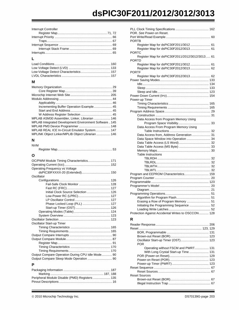
dsPIC30F2011/2012/3012/3013
Interrupt ControllerRegister Map......................................................... 71, 72Interrupt Priority .................................................................. 66
Traps........................................................................... 67Interrupt Sequence ............................................................. 69
Interrupt Stack Frame ................................................. 69Interrupts............................................................................. 65
LLoad Conditions ................................................................ 160Low Voltage Detect (LVD) ................................................ 133Low-Voltage Detect Characteristics .................................. 157LVDL Characteristics ........................................................ 157
MMemory Organization.......................................................... 29
Core Register Map...................................................... 39Microchip Internet Web Site .............................................. 205Modulo Addressing ............................................................. 44
Applicability ................................................................. 46Incrementing Buffer Operation Example..................... 45Start and End Address................................................ 45W Address Register Selection .................................... 45
MPLAB ASM30 Assembler, Linker, Librarian ................... 146MPLAB Integrated Development Environment Software .. 145MPLAB PM3 Device Programmer .................................... 148MPLAB REAL ICE In-Circuit Emulator System................. 147MPLINK Object Linker/MPLIB Object Librarian ................ 146
NNVM
Register Map............................................................... 53
OOC/PWM Module Timing Characteristics.......................... 171Operating Current (IDD)..................................................... 152Operating Frequency vs Voltage
dsPIC30FXXXX-20 (Extended)................................. 150Oscillator
Configurations........................................................... 126Fail-Safe Clock Monitor .................................... 128Fast RC (FRC).................................................. 127Initial Clock Source Selection ........................... 126Low-Power RC (LPRC)..................................... 127LP Oscillator Control ......................................... 127Phase Locked Loop (PLL) ................................ 127Start-up Timer (OST) ........................................ 126
Operating Modes (Table) .......................................... 124System Overview ...................................................... 123
Oscillator Selection ........................................................... 123Oscillator Start-up Timer
Timing Characteristics .............................................. 165Timing Requirements................................................ 165
Output Compare Interrupts ................................................. 90Output Compare Module..................................................... 87
Register Map............................................................... 91Timing Characteristics .............................................. 170Timing Requirements................................................ 170
Output Compare Operation During CPU Idle Mode............ 90Output Compare Sleep Mode Operation ............................ 90
PPackaging Information ...................................................... 187
Marking ............................................................. 187, 188Peripheral Module Disable (PMD) Registers .................... 135Pinout Descriptions ............................................................. 16
PLL Clock Timing Specifications ...................................... 162POR. See Power-on Reset.Port Write/Read Example ................................................... 60PORTB
Register Map for dsPIC30F2011/3012 ....................... 61Register Map for dsPIC30F2012/3013 ....................... 61
PORTCRegister Map for dsPIC30F2011/2012/3012/3013 ..... 61
PORTDRegister Map for dsPIC30F2011/3012 ....................... 61Register Map for dsPIC30F2012/3013 ....................... 62
PORTFRegister Map for dsPIC30F2012/3013 ....................... 62
Power Saving Modes........................................................ 133Idle............................................................................ 134Sleep ........................................................................ 133Sleep and Idle........................................................... 123
Power-Down Current (IPD)................................................ 154Power-up Timer
Timing Characteristics .............................................. 165Timing Requirements ............................................... 165
Program Address Space..................................................... 29Construction ............................................................... 31Data Access from Program Memory Using
Program Space Visibility..................................... 33Data Access From Program Memory Using
Table Instructions ............................................... 32Data Access from, Address Generation ..................... 31Data Space Window into Operation ........................... 34Data Table Access (LS Word) .................................... 32Data Table Access (MS Byte) .................................... 33Memory Maps............................................................. 30Table Instructions
TBLRDH ............................................................. 32TBLRDL.............................................................. 32TBLWTH............................................................. 32TBLWTL ............................................................. 32
Program and EEPROM Characteristics............................ 159Program Counter ................................................................ 20Programmable .................................................................. 123Programmer’s Model .......................................................... 20
Diagram ...................................................................... 21Programming Operations.................................................... 51
Algorithm for Program Flash....................................... 51Erasing a Row of Program Memory ........................... 51Initiating the Programming Sequence ........................ 52Loading Write Latches................................................ 52
Protection Against Accidental Writes to OSCCON........... 128
RReader Response............................................................. 206Reset ........................................................................ 123, 129
BOR, Programmable ................................................ 131Brown-out Reset (BOR)............................................ 123Oscillator Start-up Timer (OST)................................ 123POR
Operating without FSCM and PWRT................ 131With Long Crystal Start-up Time ...................... 131
POR (Power-on Reset)............................................. 129Power-on Reset (POR)............................................. 123Power-up Timer (PWRT) .......................................... 123
Reset Sequence ................................................................. 67Reset Sources ............................................................ 67
Reset SourcesBrown-out Reset (BOR).............................................. 67Illegal Instruction Trap ................................................ 67
© 2010 Microchip Technology Inc. DS70139G-page 203
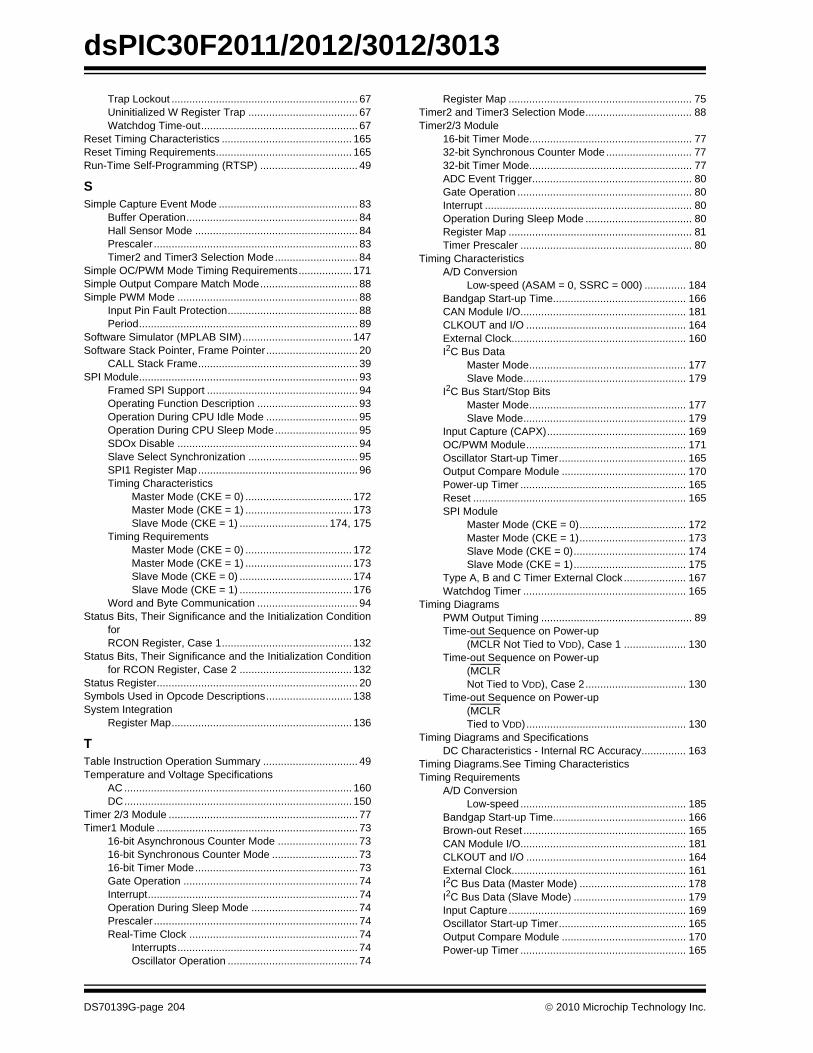
dsPIC30F2011/2012/3012/3013
Trap Lockout ............................................................... 67Uninitialized W Register Trap ..................................... 67Watchdog Time-out..................................................... 67Reset Timing Characteristics ............................................ 165Reset Timing Requirements.............................................. 165Run-Time Self-Programming (RTSP) ................................. 49
SSimple Capture Event Mode ............................................... 83
Buffer Operation.......................................................... 84Hall Sensor Mode ....................................................... 84Prescaler ..................................................................... 83Timer2 and Timer3 Selection Mode............................ 84
Simple OC/PWM Mode Timing Requirements.................. 171Simple Output Compare Match Mode................................. 88Simple PWM Mode ............................................................. 88
Input Pin Fault Protection............................................ 88Period.......................................................................... 89
Software Simulator (MPLAB SIM)..................................... 147Software Stack Pointer, Frame Pointer............................... 20
CALL Stack Frame...................................................... 39SPI Module.......................................................................... 93
Framed SPI Support ................................................... 94Operating Function Description .................................. 93Operation During CPU Idle Mode ............................... 95Operation During CPU Sleep Mode............................ 95SDOx Disable ............................................................. 94Slave Select Synchronization ..................................... 95SPI1 Register Map...................................................... 96Timing Characteristics
Master Mode (CKE = 0) .................................... 172Master Mode (CKE = 1) .................................... 173Slave Mode (CKE = 1) .............................. 174, 175
Timing RequirementsMaster Mode (CKE = 0) .................................... 172Master Mode (CKE = 1) .................................... 173Slave Mode (CKE = 0) ...................................... 174Slave Mode (CKE = 1) ...................................... 176
Word and Byte Communication .................................. 94Status Bits, Their Significance and the Initialization Condition
for RCON Register, Case 1............................................ 132
Status Bits, Their Significance and the Initialization Conditionfor RCON Register, Case 2 ...................................... 132
Status Register.................................................................... 20Symbols Used in Opcode Descriptions............................. 138System Integration
Register Map............................................................. 136
TTable Instruction Operation Summary ................................ 49Temperature and Voltage Specifications
AC ............................................................................. 160DC............................................................................. 150
Timer 2/3 Module ................................................................ 77Timer1 Module .................................................................... 73
16-bit Asynchronous Counter Mode ........................... 7316-bit Synchronous Counter Mode ............................. 7316-bit Timer Mode....................................................... 73Gate Operation ........................................................... 74Interrupt....................................................................... 74Operation During Sleep Mode .................................... 74Prescaler ..................................................................... 74Real-Time Clock ......................................................... 74
Interrupts............................................................. 74Oscillator Operation ............................................ 74
Register Map .............................................................. 75Timer2 and Timer3 Selection Mode.................................... 88Timer2/3 Module
16-bit Timer Mode....................................................... 7732-bit Synchronous Counter Mode............................. 7732-bit Timer Mode....................................................... 77ADC Event Trigger...................................................... 80Gate Operation ........................................................... 80Interrupt ...................................................................... 80Operation During Sleep Mode .................................... 80Register Map .............................................................. 81Timer Prescaler .......................................................... 80
Timing CharacteristicsA/D Conversion
Low-speed (ASAM = 0, SSRC = 000) .............. 184Bandgap Start-up Time............................................. 166CAN Module I/O........................................................ 181CLKOUT and I/O ...................................................... 164External Clock........................................................... 160I2C Bus Data
Master Mode..................................................... 177Slave Mode....................................................... 179
I2C Bus Start/Stop BitsMaster Mode..................................................... 177Slave Mode....................................................... 179
Input Capture (CAPX)............................................... 169OC/PWM Module...................................................... 171Oscillator Start-up Timer........................................... 165Output Compare Module .......................................... 170Power-up Timer ........................................................ 165Reset ........................................................................ 165SPI Module
Master Mode (CKE = 0).................................... 172Master Mode (CKE = 1).................................... 173Slave Mode (CKE = 0)...................................... 174Slave Mode (CKE = 1)...................................... 175
Type A, B and C Timer External Clock ..................... 167Watchdog Timer ....................................................... 165
Timing DiagramsPWM Output Timing ................................................... 89Time-out Sequence on Power-up
(MCLR Not Tied to VDD), Case 1 ..................... 130Time-out Sequence on Power-up
(MCLR Not Tied to VDD), Case 2.................................. 130
Time-out Sequence on Power-up (MCLR Tied to VDD)...................................................... 130
Timing Diagrams and SpecificationsDC Characteristics - Internal RC Accuracy............... 163
Timing Diagrams.See Timing CharacteristicsTiming Requirements
A/D ConversionLow-speed ........................................................ 185
Bandgap Start-up Time............................................. 166Brown-out Reset ....................................................... 165CAN Module I/O........................................................ 181CLKOUT and I/O ...................................................... 164External Clock........................................................... 161I2C Bus Data (Master Mode) .................................... 178I2C Bus Data (Slave Mode) ...................................... 179Input Capture............................................................ 169Oscillator Start-up Timer........................................... 165Output Compare Module .......................................... 170Power-up Timer ........................................................ 165
DS70139G-page 204 © 2010 Microchip Technology Inc.
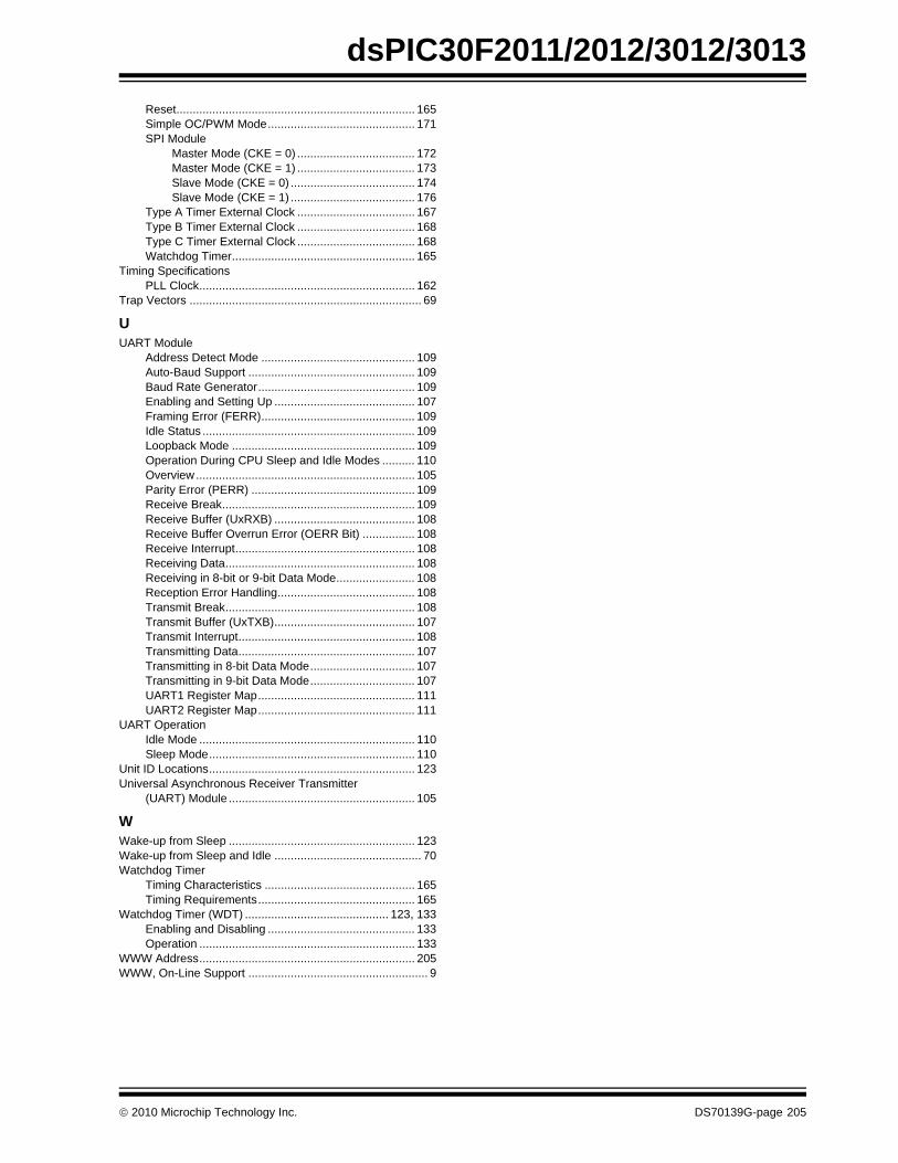
dsPIC30F2011/2012/3012/3013
Reset......................................................................... 165Simple OC/PWM Mode............................................. 171SPI ModuleMaster Mode (CKE = 0) .................................... 172Master Mode (CKE = 1) .................................... 173Slave Mode (CKE = 0) ...................................... 174Slave Mode (CKE = 1) ...................................... 176
Type A Timer External Clock .................................... 167Type B Timer External Clock .................................... 168Type C Timer External Clock .................................... 168Watchdog Timer........................................................ 165
Timing SpecificationsPLL Clock.................................................................. 162
Trap Vectors ....................................................................... 69
UUART Module
Address Detect Mode ............................................... 109Auto-Baud Support ................................................... 109Baud Rate Generator................................................ 109Enabling and Setting Up ........................................... 107Framing Error (FERR)............................................... 109Idle Status ................................................................. 109Loopback Mode ........................................................ 109Operation During CPU Sleep and Idle Modes .......... 110Overview ................................................................... 105Parity Error (PERR) .................................................. 109Receive Break........................................................... 109Receive Buffer (UxRXB) ........................................... 108Receive Buffer Overrun Error (OERR Bit) ................ 108Receive Interrupt....................................................... 108Receiving Data.......................................................... 108Receiving in 8-bit or 9-bit Data Mode........................ 108Reception Error Handling.......................................... 108Transmit Break.......................................................... 108Transmit Buffer (UxTXB)........................................... 107Transmit Interrupt...................................................... 108Transmitting Data...................................................... 107Transmitting in 8-bit Data Mode................................ 107Transmitting in 9-bit Data Mode................................ 107UART1 Register Map................................................ 111UART2 Register Map................................................ 111
UART OperationIdle Mode .................................................................. 110Sleep Mode............................................................... 110
Unit ID Locations............................................................... 123Universal Asynchronous Receiver Transmitter
(UART) Module ......................................................... 105
WWake-up from Sleep ......................................................... 123Wake-up from Sleep and Idle ............................................. 70Watchdog Timer
Timing Characteristics .............................................. 165Timing Requirements................................................ 165
Watchdog Timer (WDT) ............................................ 123, 133Enabling and Disabling ............................................. 133Operation .................................................................. 133
WWW Address.................................................................. 205WWW, On-Line Support ....................................................... 9
© 2010 Microchip Technology Inc. DS70139G-page 205

dsPIC30F2011/2012/3012/3013
NOTES:DS70139G-page 206 © 2010 Microchip Technology Inc.

dsPIC30F2011/2012/3012/3013
THE MICROCHIP WEB SITEMicrochip provides online support via our WWW site atwww.microchip.com. This web site is used as a meansto make files and information easily available tocustomers. Accessible by using your favorite Internetbrowser, the web site contains the followinginformation:
• Product Support – Data sheets and errata, application notes and sample programs, design resources, user’s guides and hardware support documents, latest software releases and archived software
• General Technical Support – Frequently Asked Questions (FAQ), technical support requests, online discussion groups, Microchip consultant program member listing
• Business of Microchip – Product selector and ordering guides, latest Microchip press releases, listing of seminars and events, listings of Microchip sales offices, distributors and factory representatives
CUSTOMER CHANGE NOTIFICATION SERVICEMicrochip’s customer notification service helps keepcustomers current on Microchip products. Subscriberswill receive e-mail notification whenever there arechanges, updates, revisions or errata related to aspecified product family or development tool of interest.
To register, access the Microchip web site atwww.microchip.com. Under “Support”, click on“Customer Change Notification” and follow theregistration instructions.
CUSTOMER SUPPORTUsers of Microchip products can receive assistancethrough several channels:
• Distributor or Representative• Local Sales Office• Field Application Engineer (FAE)• Technical Support• Development Systems Information Line
Customers should contact their distributor,representative or field application engineer (FAE) forsupport. Local sales offices are also available to helpcustomers. A listing of sales offices and locations isincluded in the back of this document.
Technical support is available through the web siteat: http://support.microchip.com
© 2010 Microchip Technology Inc. DS70139G-page 207

dsPIC30F2011/2012/3012/3013
READER RESPONSEIt is our intention to provide you with the best documentation possible to ensure successful use of your Microchipproduct. If you wish to provide your comments on organization, clarity, subject matter, and ways in which ourdocumentation can better serve you, please FAX your comments to the Technical Publications Manager at(480) 792-4150.
Please list the following information, and use this outline to provide us with your comments about this document.
TO: Technical Publications ManagerRE: Reader Response
Total Pages Sent ________
From: Name
CompanyAddressCity / State / ZIP / Country
Telephone: (_______) _________ - _________
Application (optional):
Would you like a reply? Y N
Device: Literature Number:
Questions:
FAX: (______) _________ - _________
DS70139GdsPIC30F2011/2012/3012/3013
1. What are the best features of this document?
2. How does this document meet your hardware and software development needs?
3. Do you find the organization of this document easy to follow? If not, why?
4. What additions to the document do you think would enhance the structure and subject?
5. What deletions from the document could be made without affecting the overall usefulness?
6. Is there any incorrect or misleading information (what and where)?
7. How would you improve this document?
DS70139G-page 208 © 2010 Microchip Technology Inc.
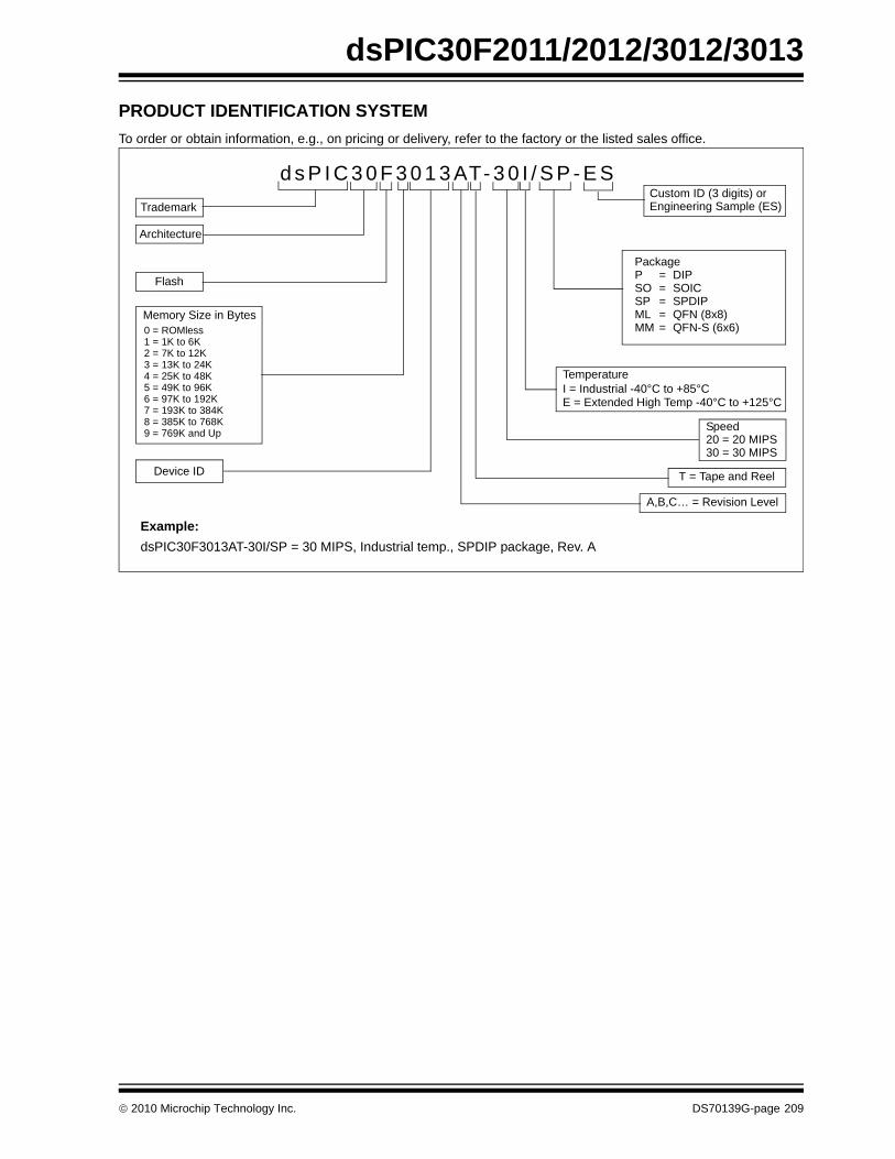
© 2010 Microchip Technology Inc. DS70139G-page 209
dsPIC30F2011/2012/3012/3013
PRODUCT IDENTIFICATION SYSTEMTo order or obtain information, e.g., on pricing or delivery, refer to the factory or the listed sales office.
d s P I C 3 0 F 3 0 1 3 AT- 3 0 I / S P - E S
Example:dsPIC30F3013AT-30I/SP = 30 MIPS, Industrial temp., SPDIP package, Rev. A
Trademark
Architecture
Flash
E = Extended High Temp -40°C to +125°CI = Industrial -40°C to +85°CTemperature
Device ID
PackageP = DIPSO = SOICSP = SPDIPML = QFN (8x8)MM = QFN-S (6x6)
Memory Size in Bytes0 = ROMless1 = 1K to 6K2 = 7K to 12K3 = 13K to 24K4 = 25K to 48K5 = 49K to 96K6 = 97K to 192K7 = 193K to 384K8 = 385K to 768K9 = 769K and Up
Custom ID (3 digits) or
T = Tape and Reel
A,B,C… = Revision Level
Engineering Sample (ES)
Speed20 = 20 MIPS30 = 30 MIPS

DS70139G-page 210 © 2010 Microchip Technology Inc.
AMERICASCorporate Office2355 West Chandler Blvd.Chandler, AZ 85224-6199Tel: 480-792-7200 Fax: 480-792-7277Technical Support: http://support.microchip.comWeb Address: www.microchip.comAtlantaDuluth, GA Tel: 678-957-9614 Fax: 678-957-1455BostonWestborough, MA Tel: 774-760-0087 Fax: 774-760-0088ChicagoItasca, IL Tel: 630-285-0071 Fax: 630-285-0075ClevelandIndependence, OH Tel: 216-447-0464 Fax: 216-447-0643DallasAddison, TX Tel: 972-818-7423 Fax: 972-818-2924DetroitFarmington Hills, MI Tel: 248-538-2250Fax: 248-538-2260KokomoKokomo, IN Tel: 765-864-8360Fax: 765-864-8387Los AngelesMission Viejo, CA Tel: 949-462-9523 Fax: 949-462-9608Santa ClaraSanta Clara, CA Tel: 408-961-6444Fax: 408-961-6445TorontoMississauga, Ontario, CanadaTel: 905-673-0699 Fax: 905-673-6509
ASIA/PACIFICAsia Pacific OfficeSuites 3707-14, 37th FloorTower 6, The GatewayHarbour City, KowloonHong KongTel: 852-2401-1200Fax: 852-2401-3431Australia - SydneyTel: 61-2-9868-6733Fax: 61-2-9868-6755China - BeijingTel: 86-10-8528-2100 Fax: 86-10-8528-2104China - ChengduTel: 86-28-8665-5511Fax: 86-28-8665-7889China - ChongqingTel: 86-23-8980-9588Fax: 86-23-8980-9500China - Hong Kong SARTel: 852-2401-1200 Fax: 852-2401-3431China - NanjingTel: 86-25-8473-2460Fax: 86-25-8473-2470China - QingdaoTel: 86-532-8502-7355Fax: 86-532-8502-7205China - ShanghaiTel: 86-21-5407-5533 Fax: 86-21-5407-5066China - ShenyangTel: 86-24-2334-2829Fax: 86-24-2334-2393China - ShenzhenTel: 86-755-8203-2660 Fax: 86-755-8203-1760China - WuhanTel: 86-27-5980-5300Fax: 86-27-5980-5118China - XianTel: 86-29-8833-7252Fax: 86-29-8833-7256China - XiamenTel: 86-592-2388138 Fax: 86-592-2388130China - ZhuhaiTel: 86-756-3210040 Fax: 86-756-3210049
ASIA/PACIFICIndia - BangaloreTel: 91-80-3090-4444 Fax: 91-80-3090-4123India - New DelhiTel: 91-11-4160-8631Fax: 91-11-4160-8632India - PuneTel: 91-20-2566-1512Fax: 91-20-2566-1513Japan - YokohamaTel: 81-45-471- 6166 Fax: 81-45-471-6122Korea - DaeguTel: 82-53-744-4301Fax: 82-53-744-4302Korea - SeoulTel: 82-2-554-7200Fax: 82-2-558-5932 or 82-2-558-5934Malaysia - Kuala LumpurTel: 60-3-6201-9857Fax: 60-3-6201-9859Malaysia - PenangTel: 60-4-227-8870Fax: 60-4-227-4068Philippines - ManilaTel: 63-2-634-9065Fax: 63-2-634-9069SingaporeTel: 65-6334-8870Fax: 65-6334-8850Taiwan - Hsin ChuTel: 886-3-6578-300Fax: 886-3-6578-370Taiwan - KaohsiungTel: 886-7-213-7830Fax: 886-7-330-9305Taiwan - TaipeiTel: 886-2-2500-6610 Fax: 886-2-2508-0102Thailand - BangkokTel: 66-2-694-1351Fax: 66-2-694-1350
EUROPEAustria - WelsTel: 43-7242-2244-39Fax: 43-7242-2244-393Denmark - CopenhagenTel: 45-4450-2828 Fax: 45-4485-2829France - ParisTel: 33-1-69-53-63-20 Fax: 33-1-69-30-90-79Germany - MunichTel: 49-89-627-144-0 Fax: 49-89-627-144-44Italy - Milan Tel: 39-0331-742611 Fax: 39-0331-466781Netherlands - DrunenTel: 31-416-690399 Fax: 31-416-690340Spain - MadridTel: 34-91-708-08-90Fax: 34-91-708-08-91UK - WokinghamTel: 44-118-921-5869Fax: 44-118-921-5820
Worldwide Sales and Service
08/04/10