Embed Size (px)
Citation preview
(Ref.No.;NO.IGBT-HI-00002 R2)
(HIGH VOLTAGE IGBT MODULE)
Application Manual
Hitachi Power Semiconductor Device, Ltd.
Issued on Dec.2009
2009. Hitachi Power Semiconductor Device, Ltd.

- Important Notices - The handler of the Hitachi high-voltage IGBT module (hereinafter, this product) is advised to
keep this manual within reach. Refer to the "Contract" separately for details on the agreement and warranty for this product.
The handler of this product is advised to thoroughly read this manual and the relevant materials that are referenced in this manual before use, and properly use the product in accordance with the product knowledge, safety information and precautions, and instructions on operation and handling, etc.
Always operate within the maximum values stated in the specifications in this manual. Also perform proper inspection and maintenance to prevent failure. In no event shall Hitachi be liable for any failure with a Hitachi IGBT module or any secondary damage resulting from use at a value exceeding the absolute maximum rating or that may result from a natural disaster or any other force majeure.
Do not operate, handle or modify this product in any way that deviates from the methods specified in this manual. It may cause the product to fail or result in a fatal accident. Hitachi assumes no responsibility for any accident that may result under these circumstances. Hitachi assumes no responsibility for any intellectual property claims or any other issue that may result from information, products, or circuits described in this manual.
If there are any questions or concerns about the contents of this manual that are not clear, please contact the nearest Hitachi branch office or the departments listed below (or a dispatched Hitachi representative).
The intellectual property rights on the contents of this manual belong to Hitachi. Disclosure of this manual in any form, in whole or in part, to third parties without the expressed written permission of Hitachi Power Semiconductor Device, Ltd. is forbidden.
The product specifications and dimensions listed on this manual are subject to change without prior notice to accommodate technology changes which affect product characteristics. Please contact our sales department if necessary when placing an order, and refer to the catalog or specifications sheet with the latest specifications and precautions.
No license is granted by this manual under any patents or other rights of any third party or Hitachi.
This manual may not be reproduced or duplicated, in whole or in part, without the expressed written permission of Hitachi Power Semiconductor Device, Ltd.
When disposing of semiconductor devices and packaging materials, please follow the local laws and regulations of the respective countries.
The products (technologies) described in this manual are not to be provided to any party whose purpose in their application will hinder maintenance of international peace and safety nor are they to be applied to that purpose by their direct purchasers or any third party. When exporting these products (technologies), all necessary procedures are to be taken in accordance with foreign exchange laws.
In the event of operation failure or problems, please contact the department in charge or the nearest Hitachi branch office with the following information immediately.
The nameplate or the specifications (product name, serial number, capacity, model, and production date) of the product
Problem details (with as much detail as possible, describe the state before and after the problem occurred)
Hitachi Power Semiconductor Device, Ltd. 5-2-2 Omika-cho Hitachi City, Ibaraki Prefecture, Japan 319-1221 TEL: +81-294-55-6841(Direct) FAX: +81-294-55-9953
Safety Precautions
Before using the Hitachi IGBT modules, please thoroughly read this manual and refer to its diagrams
and materials for proper use. Be sure to familiarize yourself with knowledge of the device, safety
information, and all precautions before use.
In this manual, safety precautions are ranked as "WARNING" or "CAUTION."
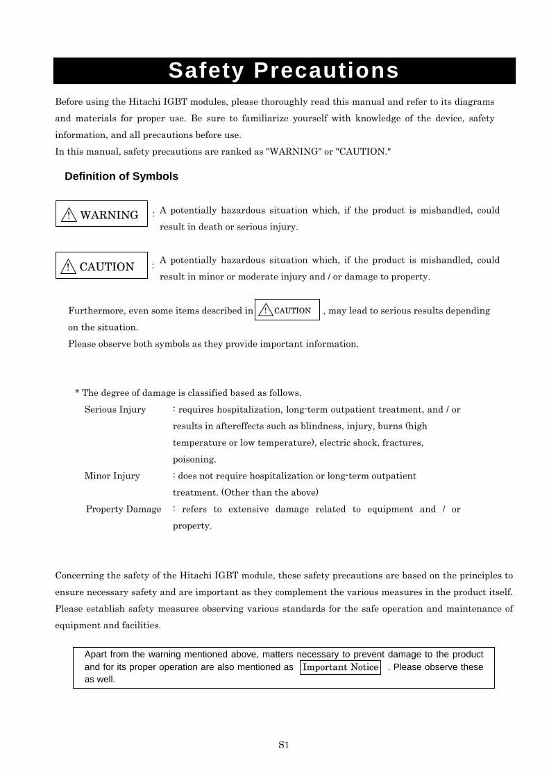
Definition of Symbols
A potentially hazardous situation which, if the product is mishandled, could
result in death or serious injury. : ! WARNING
A potentially hazardous situation which, if the product is mishandled, could
result in minor or moderate injury and / or damage to property. : ! CAUTION
Furthermore, even some items described in , may lead to serious results depending
on the situation.
Please observe both symbols as they provide important information.
* The degree of damage is classified based as follows.
Serious Injury : requires hospitalization, long-term outpatient treatment, and / or
results in aftereffects such as blindness, injury, burns (high
temperature or low temperature), electric shock, fractures,
poisoning.
Minor Injury : does not require hospitalization or long-term outpatient
treatment. (Other than the above)
Property Damage : refers to extensive damage related to equipment and / or property.
Concerning the safety of the Hitachi IGBT module, these safety precautions are based on the principles to
ensure necessary safety and are important as they complement the various measures in the product itself.
Please establish safety measures observing various standards for the safe operation and maintenance of
equipment and facilities.
Apart from the warning mentioned above, matters necessary to prevent damage to the product and for its proper operation are also mentioned as Important Notice . Please observe these as well.
! CAUTION
S1
S a f e t y P r e c a u t i o n s ( C o n t i n u e d )
<General Precautions>
● Semiconductor devices may experience failures due to accidents or unexpected surge voltages.
Accordingly, you should always adopt fail-safe design techniques, redundancy, etc. to avoid
extensive damage in the event of failure.
● Semiconductor devices were not specifically designed as a device to be used in life-threatening
situations.
For those applications where extremely high reliability is required (such as nuclear power control,
aerospace and aviation, transportation equipment, life-support-related medical equipment, fuel
control equipment, and various kinds of safety equipment), use a semiconductor device with
extremely high reliability and incorporate fail-safe precautions and other safety measures. In
addition, please consult Hitachi's sales department staff in such cases.
(If the semiconductor devices fail, its wiring, wiring patterns, etc. may emit smoke or catch on fire
or the semiconductor device itself may burst as a result.)
● High Current Load Test
Please perform an actual loading test that covers current, voltage, frequency, pulse width
conditions, etc. that may occur when actually using the equipment.
S2
S a f e t y P r e c a u t i o n s ( C o n t i n u e d )
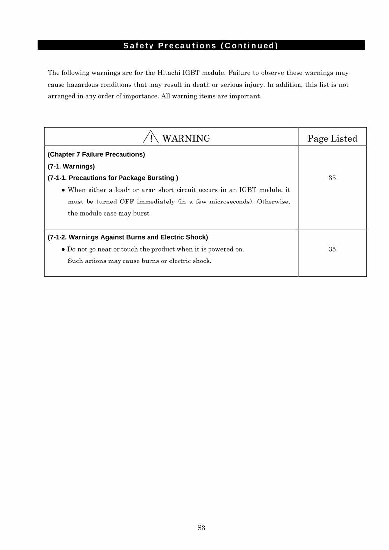
The following warnings are for the Hitachi IGBT module. Failure to observe these warnings may
cause hazardous conditions that may result in death or serious injury. In addition, this list is not
arranged in any order of importance. All warning items are important.
! WARNING Page Listed (Chapter 7 Failure Precautions)
(7-1. Warnings)
(7-1-1. Precautions for Package Bursting )
● When either a load- or arm- short circuit occurs in an IGBT module, it
must be turned OFF immediately (in a few microseconds). Otherwise,
the module case may burst.
35
(7-1-2. Warnings Against Burns and Electric Shock)
● Do not go near or touch the product when it is powered on.
Such actions may cause burns or electric shock.
35
S3
S a f e t y P r e c a u t i o n s ( C o n t i n u e d )
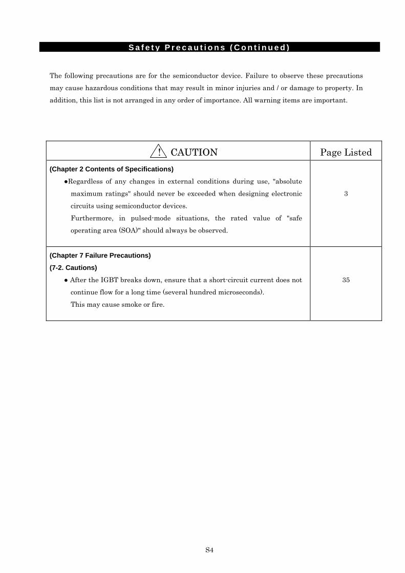
The following precautions are for the semiconductor device. Failure to observe these precautions
may cause hazardous conditions that may result in minor injuries and / or damage to property. In
addition, this list is not arranged in any order of importance. All warning items are important.
! CAUTION Page Listed (Chapter 2 Contents of Specifications)
●Regardless of any changes in external conditions during use, "absolute
maximum ratings" should never be exceeded when designing electronic
circuits using semiconductor devices.
Furthermore, in pulsed-mode situations, the rated value of "safe
operating area (SOA)" should always be observed.
3
(Chapter 7 Failure Precautions)
(7-2. Cautions)
● After the IGBT breaks down, ensure that a short-circuit current does not
continue flow for a long time (several hundred microseconds).
This may cause smoke or fire.
35
S4
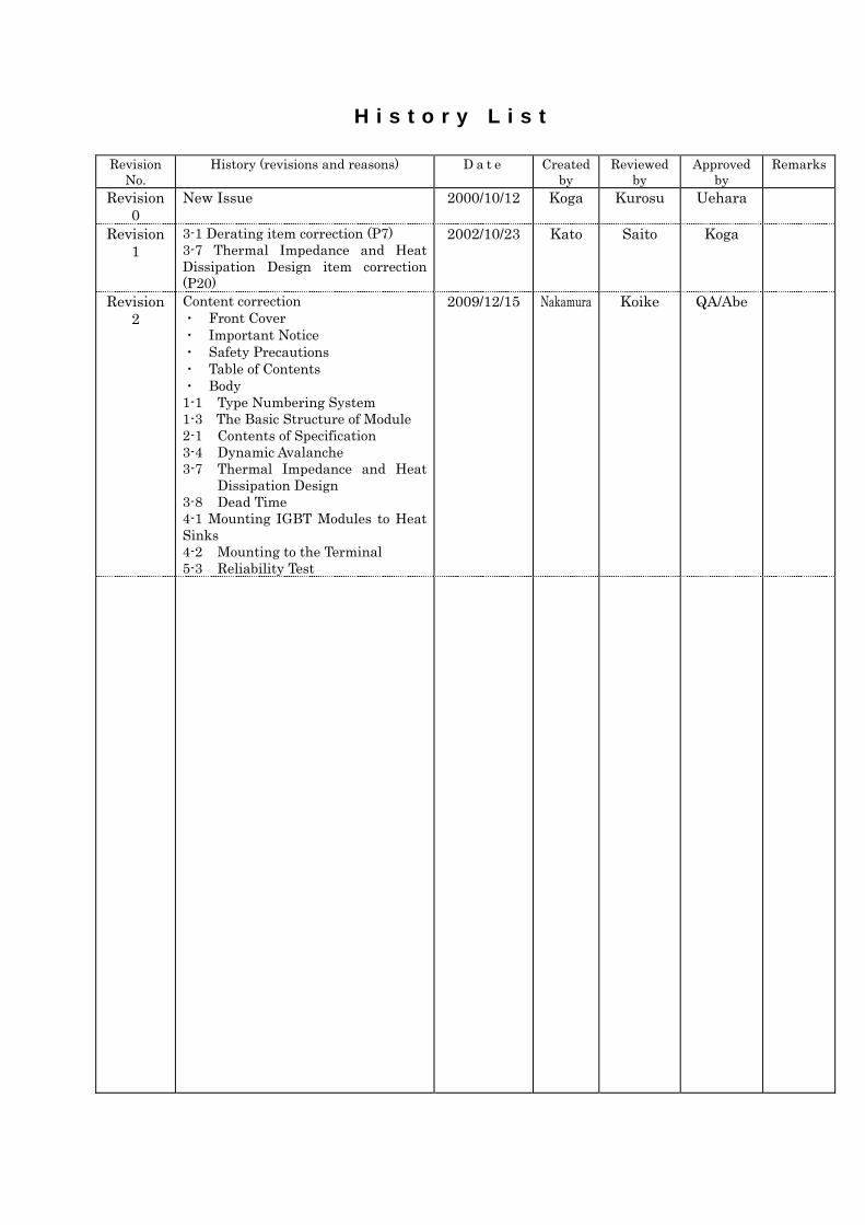
H i s t o r y L i s t
Revision No.
History (revisions and reasons) D a t e Created by
Reviewed by
Approved by
Remarks
Revision 0
New Issue 2000/10/12 Koga Kurosu Uehara
Revision 1
3-1 Derating item correction (P7) 3-7 Thermal Impedance and Heat Dissipation Design item correction (P20)
2002/10/23 Kato Saito Koga
Revision 2
Content correction ・ Front Cover ・ Important Notice ・ Safety Precautions ・ Table of Contents ・ Body 1-1 Type Numbering System 1-3 The Basic Structure of Module 2-1 Contents of Specification 3-4 Dynamic Avalanche 3-7 Thermal Impedance and Heat
Dissipation Design 3-8 Dead Time 4-1 Mounting IGBT Modules to Heat Sinks 4-2 Mounting to the Terminal 5-3 Reliability Test
2009/12/15 Nakamura Koike QA/Abe
-i-
I n t r o d u c t i o n
This manual is a written explanation of the specifications of the IGBT module, a type of
semiconductor device, its tables of characteristics, external dimensional drawings, and precautions for
use. It is intended for people who are familiar with the testing of the IGBT module itself, or the design,
manufacture, or testing of inverters or other electrical equipment that use the IGBT module. In
addition, in order to use and clearly understand the contents of this manual, it requires a level of
knowledge or education equivalent to a graduate of a technical high school who enrolled in an electrical
engineering course.
The IGBT module is the voltage control type semiconductor switch for controlling the on-off of the
main circuit current by controlling the voltage applied to the gate.
This manual describes methods of handling required in order for the IGBT module to function
smoothly and safely.
This manual is subject to change without prior notice to accommodate technology changes which
affect product characteristics.
For latest information (details about the individual specifications and application of each product),
please refer to the following website.
(http://www.hitachi-power-semiconductor-device.co.jp/en/)
If there is anything unclear, please contact our sales office.
Explanation of Terms and Abbreviations
Please refer to the table below for the meanings of terms and abbreviations used in this manual.
Terminology and
Abbreviations
Original Term Definition
IGBT Insulated Gate Bipolar Transistor Insulated Gate Bipolar Transistor
MOSFET Metal Oxide Semiconductor Field
Effect Transistor
Metal Oxide Semiconductor Field Effect
Transistor
FWD Fly Wheel Diode Fly Wheel Diode
*Here, refers to the diode connected in reverse
order with the IGBT
RBSOA Reverse Biased Safe Operating
Area
Reverse Biased Safe Operating Area
-ii-
Organization of this Manual
This manual is a written explanation of the specifications of the IGBT module, a type of
semiconductor device, its tables of characteristics, external dimensional drawings, and precautions for
use. *These instructions should be read and clearly understood before use, and the IGBT module should
be used accordingly by people who are familiar with the testing of the IGBT module itself, or the design,
manufacture, or testing of inverters or other electrical equipment that use the IGBT module.
The contents of this manual are organized as follows.
Chapter 1 IGBT module: Explanation of the IGBT module numbering system, structure, and
operating principles
Chapter 2 Specification items: Explanation of specification items mentioned
Chapter 3 Precautions for use: Explanation of precautions to be observed when using the IGBT
module
Chapter 4 Precautions on mounting: Explanation of precautions to be observed when mounting
the IGBT module
Chapter 5 Reliability: Explanation of the reliability of and quality assurance for the IGBT
module
Chapter 6 Troubleshooting: Explanation of the IGBT module's failure mode and methods of
checking for electrical characteristics during breakdown
Chapter 7 Failure Precautions: Explanation of safety precautions when failures related to the
IGBT module occur
-iii-
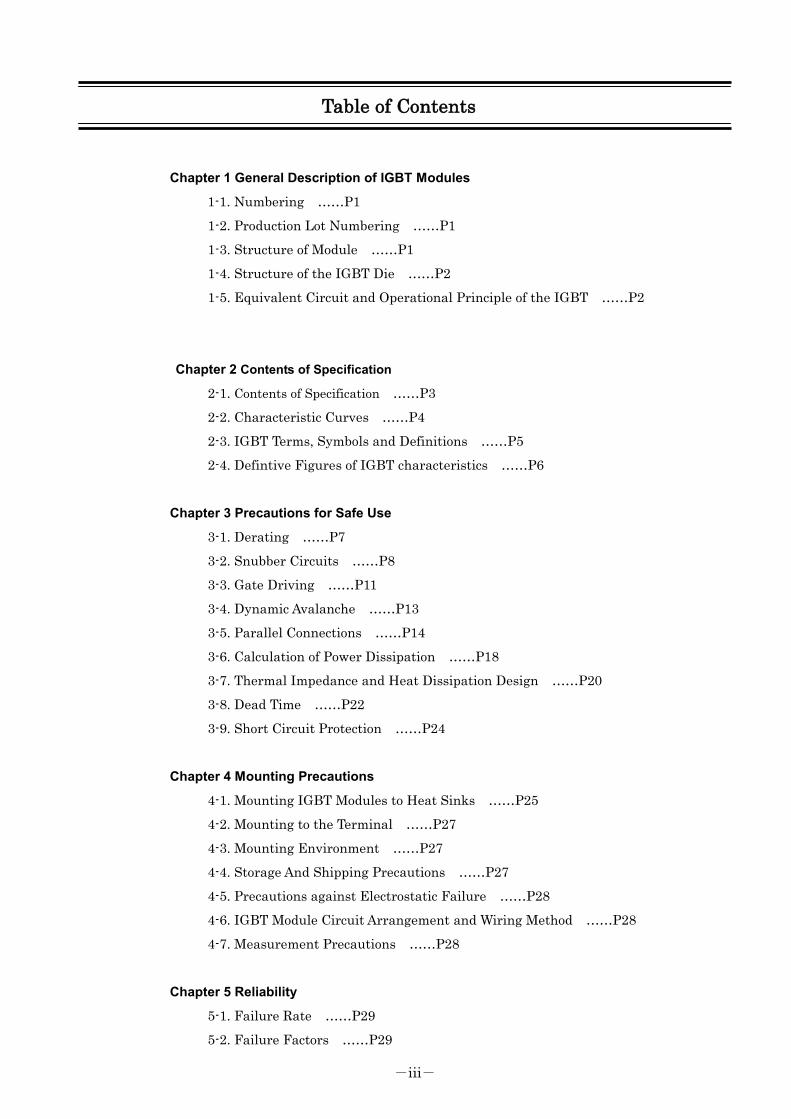
Table of Contents
Chapter 1 General Description of IGBT Modules
1-1. Numbering ……P1
1-2. Production Lot Numbering ……P1
1-3. Structure of Module ……P1
1-4. Structure of the IGBT Die ……P2
1-5. Equivalent Circuit and Operational Principle of the IGBT ……P2
Chapter 2 Contents of Specification
2-1. Contents of Specification ……P3
2-2. Characteristic Curves ……P4
2-3. IGBT Terms, Symbols and Definitions ……P5
2-4. Defintive Figures of IGBT characteristics ……P6
Chapter 3 Precautions for Safe Use
3-1. Derating ……P7
3-2. Snubber Circuits ……P8
3-3. Gate Driving ……P11
3-4. Dynamic Avalanche ……P13
3-5. Parallel Connections ……P14
3-6. Calculation of Power Dissipation ……P18
3-7. Thermal Impedance and Heat Dissipation Design ……P20
3-8. Dead Time ……P22
3-9. Short Circuit Protection ……P24
Chapter 4 Mounting Precautions
4-1. Mounting IGBT Modules to Heat Sinks ……P25
4-2. Mounting to the Terminal ……P27
4-3. Mounting Environment ……P27
4-4. Storage And Shipping Precautions ……P27
4-5. Precautions against Electrostatic Failure ……P28
4-6. IGBT Module Circuit Arrangement and Wiring Method ……P28
4-7. Measurement Precautions ……P28
Chapter 5 Reliability
5-1. Failure Rate ……P29
5-2. Failure Factors ……P29

-iv-
5-3. Reliability Test ……P30
5-4. Quality Assurance System Diagram ……P32
Chapter 6 Troubleshooting
6-1. IGBT Failure Modes (Electrical Failure Mode) ……P33
6-2. Device Check Method ……P34
Chapter 7 Failure Precautions
7-1. Warnings ……P35
7-2. Cautions ……P35
-v-
L i s t o f F i g u r e s
Figure No. Name Page No.
Figure 1.1 Basic Structures of an IGBT Module ······················································· -1-
Figure 1.2 Structure of an IGBT Die ··································································· -2-
Figure 1.3 Equivalent Circuit ·············································································· -2-
Figure 1.4 Operational Description ······································································· -2-
Figure 2.1 Definition of IGBT Switching Characteristics (ton, toff) ······························ -6-
Figure 2.2 Definition of FWD Reverse-Recovery Characteristics (trr) ························· -6-
Figure 3.1 Features of Various Snubber Circuits ····················································· -8-
Figure 3.2 Turn-OFF Mode of Bottom Arm IGBT ···················································· -8-
Figure 3.3 Equivalent Circuit in a Transient State ··················································· -8-
Figure 3.4 IGBT Module Current (Ic) and Voltage (VCE) Waveforms with Snubber Circuit -9-
Figure 3.5 Waveforms of Each Snubber Circuit Part ·············································· -9-
Figure 3.6 Example of IGBT Switching Waveform (Current and Voltage) ·················· -11-
Figure 3.7 Gate Charge (QG) Characteristics ························································· -11-
Figure 3.8 Driving Voltage and Gate Charge Characteristics ···································· -12-
Figure 3.9 Example of IGBT Turn-OFF Waveform ·················································· -13-
Figure 3.10 Example of Dynamic Avalanches Area ···················································· -13-
Figure 3.11 Example of Parallel Connection between IGBT Modules and Driver Circuit · -15-
Figure 3.12 Wiring to Equalize Main Wiring Inductance Values ·································· -16-
Figure 3.13 Equalization of Unbalanced Current ······················································ -16-
Figure 3.14 Parallel Connection Operations (without Snubber) ··································· -17-
Figure 3.15 Parallel Connection Operations (with Snubber) ······································· -17-
Figure 3.16 Ic vs. VCE Characteristic ····································································· -18-
Figure 3.17 Switching Loss vs. Collector Current ····················································· -18-
Figure 3.18 Forward Current vs. Forward Voltage ···················································· -19-
Figure 3.19 Temperature Measuring Points ····························································· -20-
Figure 3.20 Thermal Equivalent Circuit ·································································· -20-
Figure 3.21 Temperature Ripple ············································································· -21-
Figure 3.22 Transient Thermal Impedance ······························································· -21-
Figure 3.23 Inverter Operating Temperature Ripple ·················································· -21-
Figure 3.24 Typical Configuration of a Major Circuit (Single-Phase Top and Bottom Arms) -22-
Figure 3.25 Control Signal, Driver Voltage, and IGBT Collector Voltage Waveforms ······· -22-
-vi-
Figure 3.26 Verification Circuit Configuration (Half-Bridge Circuit) ······························ -23-
Figure 3.27 Control Signal and Gate Waveforms ······················································· -23-
Figure 3.28 Top and Bottom Arm Short-Circuited Waveform ········································ -23-
Figure 3.29 Short-Circuit Protection Waveforms ························································· -24-
Figure 4.1 Grease Application Method with Screen ··················································· -25-
Figure 4.2 Clamping Order for IGBT Module ··························································· -26-
Figure 4.3 Example of Improper Heat Sink Mounting ················································ -26-
Figure 4.4 Cross-Sectional View of Screw Hole ··························································· -27-
Figure 5.1 Module Failure Regions (Bathtub-Shaped Curve) ········································ -29-
Figure 6.1 Electrical Failure Analysis ····································································· -33-
-vii-
L i s t o f Ta b l e s
Table No. Name Page No.
Table 2.1 Specifications Sheet (Example) ································································· -3-
Table 2.2 Characteristic Curve Items ······································································ -4-
Table 2.3 IGBT Terms, Symbols and Definitions ······················································· -5-
Table 3.1 Example of Short-Circuit Protection ·························································· -24-
Table 4.1 Recommended Clamping Torque Values for IGBT Mounting ··························· -25-
Table 4.2 Recommended Grease and Specific Gravity ················································ -26-
Table 4.3 Recommended Mounting Hole Diameter and Chamfering Value (mm) ············ -26 -
Table 4.4 Recommended Clamping Torque for Terminals ············································ -27-
Table 4.5 Size for Screw Hole ·················································································· -27-
Table 5.1 Failure Mechanisms ················································································ -29-
Table 5.2 Reliability Test Types and Descriptions ······················································ -30-
Table 5.3 Reliability Test Types and Testing Conditions ············································· -31-
Table 5.4 Chart of Hitachi's Quality Assurance System ················································ -32-
Table 6.1 IGBT Electrical Characteristics Check Method (Reference) ··························· -34-
������
1. General Description of IGBT Modules 1-1. Numbering
������� �� ���� ��� �
�� � �
� � � � � � � � �
1-2. Production Lot Numbering �� ���� ���� ������ ������ �������������������������� ������������������� � ���������� ����� �������
����� ������ ��!"��
#������� �� $���� %� � � &� � �'�(��(��
� � � � )�� ����������������� ������ ���*�������� ��������� ���
� � � � � +����������* ����#������!�������� �, �� ������ �����* ����
�
1-3. Structure of Module����Example����single pack module���� -�!�� ��"����� ����������� ��������� �� � ������������� ���� ������������� ������.�������)/�������� 0�
�� �����*������!� ����1������ "�
� ���
��� ��� ��
���
� ����������� �
���
���� �
2��,�� �� � � �����
���������!�����
��� �������3�� ������
3�������� ������
! �
�
Figure 1.1 Basic Structures of an IGBT Module �
�
3�����*� �
�20��0�30�40�������"""������� ��
5�� ��6����! ��$�6��
��"!"��7%�0760��8%�0860�%06�
(8%(0860�'8%'086��
+��1�! ��*� �
��"!"�.%�.�!��6����! �)����������+��1�! ��*� ��
5�� ��3��� ����2��
��"!"���%�)��9��0�20����)-�9��0�2��
���� ��������������������������!��������
��%��0��%��0��%�'���0�#%�3���� ���
����� ��*� �
���%�)/��0��4%�4��� ��
������
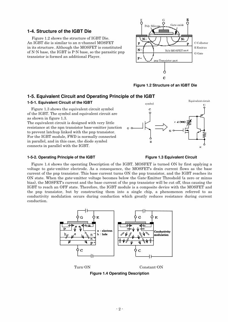
1-4. Structure of the IGBT Die
-�!�� ��"����� ���� ��������� ����)/���4� "�2��)/����� ������������������������� ���:;-������������������ "�2�����!���� ��:;-��������������� ������������ 0��� �)/������+������ 0������ ��������������������������������� ����������������+��* �"� �
�
�
�
�
� � � � � � � � � � � � � � � � � � � � � � � � � � � � � � � � � � � � � � � � � � � � � � � � � � � � � � Figure 1.2 Structure of an IGBT Die �1-5. Equivalent Circuit and Operating Principle of the IGBT 1-5-1. Equivalent Circuit of the IGBT
� � -�!�� ��"���� ���� � <����� ������������*���������� �)/��"��� ��*��������� <����� ������������� ������� �������!�� ��""� ��� � <����� ��������������� ��!� �� ����� �*������ �� ������� ������ ������������������� � ���� ��=������������� � ��������������1 �� ������ ���������������"�-����� �)/�������� 0�-, 4�����������*����� �� ����������� �0���������������� 0��� ����� ��*����� ����� ������������� �� ������ �)/��"�
�
1-5-2. Operating Principle of the IGBT � � � � Figure 1.3 Equivalent Circuit� �
� � -�!�� ��"(���� ���� ��� �����!�4 ��������������� �)/��"��:;-���������� ��:���*�����������*��!��������! � ��� !�� � ���� �� � ����� "� 2�� �� ���� <� �� 0� �� ��:;-��>�� ������ ���� ��� ��� �� ��� �� � ��� ����� �������� ���������������"��������� ����� ���������:���� ���������������0������� �)/���� ��� ������:������ "�, � ���� �!�� � ���� �������! �� ��� ��� �� ��� �/�� ������ ����� ���������? �����������������0��� ��:;-��>������ ��������� ���� ����� �������� ���������������� ����� ��������0������������!��� �)/������� �������:--����� "��� � ��� 0��� �)/�������� �������������� �� ��� � ������ ��:;-��������� � ���� ����������0� ���� �*� �����������!� �� � � ����� �� ���!� � ����0� �� �� ��� ���� � � �� �� ��� ��������������*� ����������� ������� �����!� ����������� ����� !� ���*� � ��� �� � ������� � �����!� ���� �������������"�
�
�
�� ���� ����� ���� ����� ���� �� �� ��
�� ���� �� �� ��
�� ���� ��������������
�� ���� ��
�� �� �� �� � ����� � ����� � ����� � ���������� � � � ��� ��� ��� ��� ����3����������*3����������*3����������*3����������*������������������������������������������������
��
�
Figure 1.4 Operating Description
3%3��� ����
�%����� �
/%/��
/�� ��$��
����/�
������ ��++++
���� �� ��++++ �� ��
3333
���� �� ��++++
+��*�;������
�����:;-�� ����
������������������
�
�����:�� � � 3��������:��
�
�
�*�����<����� ������������ ���� ��
�� �� �� ���� �� �� ��
�������������� �������� �������� �������� �������
�����
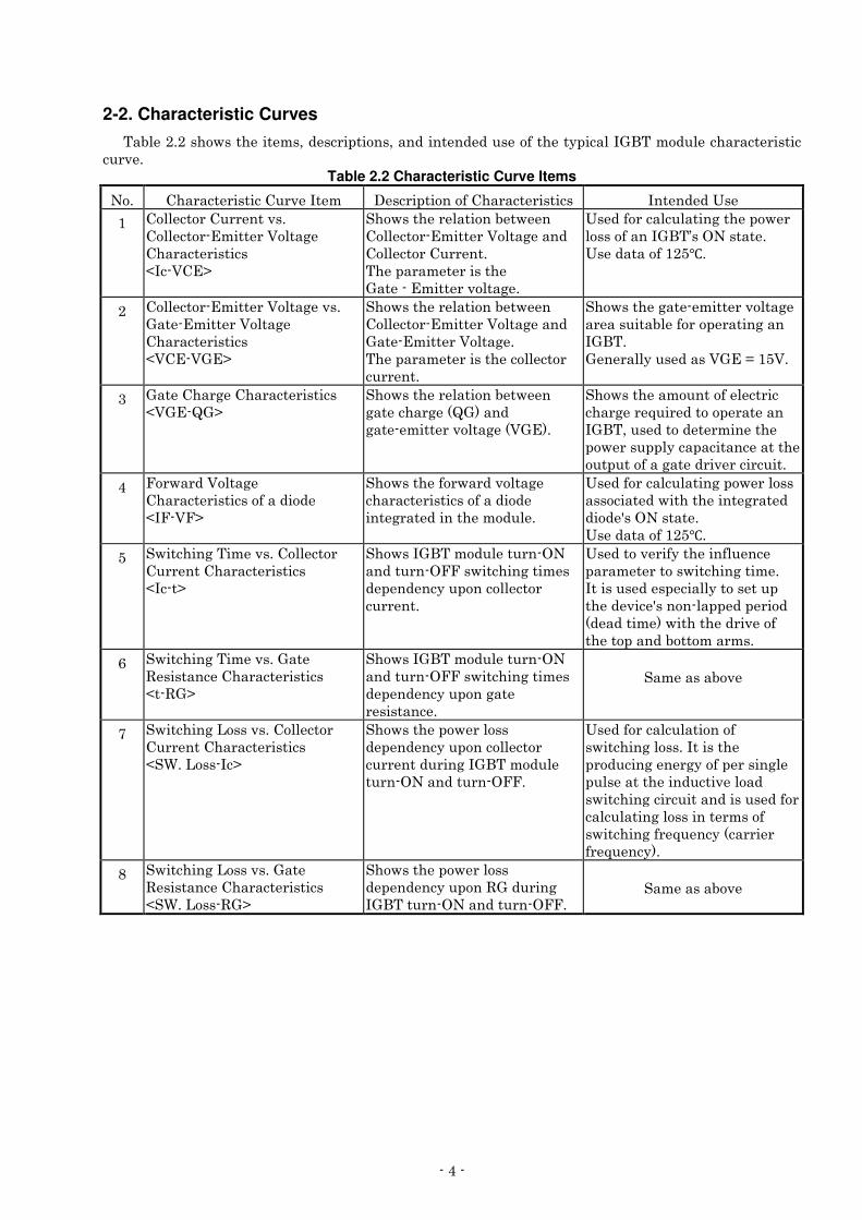
2. Contents of Specification �
@�@�@�@� ���� 32A�):�32A�):�32A�):�32A�):�����B� 5 !���� ��� ��� ��*� ����! �� ��� $� ����� ����������� �����!� �� 0� C������� � ��$����� �����!�C� �������
� � �� � � $� � �� � �� � ��!���!� � �������� ��������� ����!� � ������������ � ��� �"� -���� ���� 0� ���
���� ����� �����������0��� ���� ������ ����C��� ��� �����!��� ���;:2�C���������� �*��� ���� �� �"�
2-1. Contents of specification ���� ��"����� ����� $���� ������ ����������"� �
��� � 2������ ���$�����5����!������������� ��"���
2������ ���$����������!������*���� � �������0�� ��������������� ��������������������������� ���� � ����������� ������� � ���)/�������� �� ���������"�;����������������� �! � ����*� $�� �� ������ ��������� ���$��������������������� � ������ ��������� !��������;�� �:� �������2� ���;:2�"��)���� ������ ��� ��� �������� ��� ����� ������ �0������*��� �1��� �"��
��� �� ������3������ ������������������ ��"���
�� � � ��������������� ������������)/�������� ��� �� ����� ���� ���� ������������������������� ���� $�� �� �������$����0��*�����0����������������� �"��� � ����� ���� ������ ���������� ������������� �������D� ����� �� � ������� ������� ������0� �*������ �� ������!�� ������� ������0� ���� �� ������������ ������"�
��� :�� ���� �����������������(��������� ��"���
+� �������������� ���$����������!�������� ������ ����� ����� �"�
�� � � � � � � � � � � � � � � � � Table 2.1 Specification sheet (Example)
�
�
�
�
�
�
�
�
�
�
�
�
�
�
�
�
�
�
�
�
�
�
�
�
���
��
���
(��
;� ��������������� ��
+�������� ��
��(���
2-2. Characteristic Curves ���� ��"����� ���� ��� ��0�� ����������0�������� �� ���� ������ ��*������)/�������� �������� �������
���� "�Table 2.2 Characteristic Curve Items
��"� 3������ �������3��� �)� � � 4 �������������3������ �������� )�� �� ��A� �
�� 3��� �����3��� �����"�3��� ���������� ��6����! �3������ ��������E)��63�F�
;�� ���� �� �������� � ��3��� ���������� ��6����! �����3��� �����3��� ��"��� ������ � ������� �/�� �������� �������! "�
A� ����������������!��� ��� �������������)/��G��:������ "�A� �����������8�"�
�� 3��� ���������� ��6����! ���"�/�� ������ ��6����! �3������ ��������E63��6/�F�
;�� ���� �� �������� � ��3��� ���������� ��6����! �����/�� ������ ��6����! "��� ������ � ������� ����� ��������� ��"�
;�� ���� �!�� � ���� �������! ��� ��������� ������� �����!����)/��"�/ � ����*��� �����6/��9��86"�
� /�� �3���! �3������ ��������E6/��H/F�
;�� ���� �� �������� � ��!�� �����! ��H/������!�� � ���� �������! ��6/��"� �
;�� ���� ����������� � ����������! �� <��� ������� ��� ����)/��0��� ������ � ���� ��� ��� �������*����������� ������ �������������!�� ����� ���������"�
(� -�� ����6����! �3������ ����������������� �E)-�6-F�
;�� ���� ���� ���������! �������� ����������������� ���� !��� ������� ������ "�
A� ����������������!��� ��������������� �� ������ ���� !��� ������ >��:������ "�A� �����������8�"�
8� ; ������!���� ���"�3��� �����3��� ���3������ ��������E)���F�
;�� ��)/�������� ������:�����������:--�� ������!���� ��� � �� ��*���������� ��������� ��"�
A� ������ ���*��� ������ �� ������ � ������ ������!���� "� �)������� �� �� �����*����� ������� �� ��� >���������� ��� ������� ������ �� ������ ����� ������ ��������������������"�
'� ; ������!���� ���"�/�� �5 ������� �3������ ��������E��5/F�
;�� ��)/�������� ������:�����������:--�� ������!���� ��� � �� ��*������!�� �� ������� "�
�;�� �������� �
7� ; ������!�#������"�3��� �����3��� ���3������ ��������E;, "�#����)�F�
;�� ���� ��� �������� � �� ��*���������� ��������� ��������!�)/�������� ������:�����������:--"�
A� ���������������������� ������!�����"�)������� ���������!� � �!*����� �����!� ����� ������ ��������� ������� ������!������������������ ����������������!���������� �������� ������!��� <� ��*������� ���� <� ��*�"�
I� ; ������!�#������"�/�� �5 ������� �3������ ��������E;, "�#����5/F�
;�� ���� ��� �������� � �� ��*������5/������!�)/��������:�����������:--"�
�;�� �������� �

��8���
2-3. IGBT Terms, Symbols, and Definitions �
Table 2.3 IGBT Terms, Symbols Definitions ��5�;� ;J��:#;� 4�-)�)�):�;�
3��� ���������� ��6����! � 63�;� ��$��������� ��� ����� ����� ���� �������! ��������� ��!�� "�
/�� ������ ��6����! � 6/�;� ��$��������� ��� �!�� � ���� �������! ��������� ������ ����"�
3��� �����3��� ��� )3� , ������ ���� ��� � ���� ����� �� �� �����������0� ��$����� ���� ��� � ���� � ���43����� ���������� ������ ������"�
3��� �����+� ��4����������� +3� A�� �� �� ���� �� � ��� ����������0� ��$����� ���� ��� � ���� � ��� ������������� ������� �������������"�
K��������� �� ����� � �=� 5��! �������� ��� �� �� ����� ����=�������������������������!�"�
;����! �� �� ����� � ���!� 5��! �������� ��� �� �� ����� ����������! ����)/�������� "�
�
�
;�� ����<� �
�
�
��
��$��������� ��� ����� �����������!����<� � � ��)/�������� ����
����� �� ����� � ��� ���1� ��� �������0� ����!� �� ���� �� !� �� � ��� ��� � ��������������������"�
� � ��$��������� ��� ��������!����<� � � �� ����!���������������� �����)/�������� �� �������"�
3��� ���������� ��3�������3��� ��� )3�;� A�� �� �� ���� �� ����������0� ���� ����� ���� ��� ���� ����*��!� ���� ����� ���� �������! ���������������� "�
��� %�/�� ������ ��� ���������� ������ �"� �
/�� ������ ��# �1�! �3��� ��� )/�;� A�� ���� ���� ������������0�!�� ����� �����������*��!�!�� � ���� ��
�����! ���������������� "�
��� %�3��� ���������� ��� ���������� ������ �"� �
3��� ���������� �� �
;����������6����! �
63������� A�� ���� ���� ������������0����� ��������������������! � � ������ ��������� ���������������!"�
4 � ����!� ��� �� � ���� � �� � ��� �� � � ������� � ����0� �� � ���� � ��� ��3��� ���������� �������! �� � �������� �������������$�����*�� �������"�
/�� ������ ����� ������6����! � 6/���:�� A�� �� �� ���� �� ����������0� ���� � ��� !�� � ���� �� �����! � � �� ���� ��������� ��� ������� ��� ��� � ���� ��� ������ � !����"� �� � ���� ����� ���� ��� ��� �� �� !�����!����� ������L�������� ������ "�
)�����3��������� � 3� �� A�� ���� ���� ������������0����� �������������� �� � ��!�� ����� ���� ��� �������"�
5 � �� ������� ��3��������� � 3� �� A�� ���� ���� ������������0����� �������������� �� � ��!�� ��������� ������ �������"�
:������3��������� � 3� �� A�� �� �� ���� �� ����������0� ���� � ��� ���������� � � � �� ���� ����� ���� ���� ��� �������"�
�����:����� � ���� A�� �� �� ���� �� ����������0� ��� � � <��� �� ���� ���� ����� ���� �� �����! � ���� ���� �M���������������� ���� ���� �� �� ���� ��� � ��:��!�� � �����! ������ ��� ���M������������������ ����������!���� ����� <� ���� ������!����)/�������� ������:--����� ����:������ �������N����
�����:��4 ��*���� � ������� ��� �� <��� ���������� ��������� ������� ����&M�������������������� ���� ���� ���� ��� � ��:��!�� ������! ������ ��� ���M������������������ "�
-������� � ��� ��� �� <��� ���������� ��������� ������� ����&M�������M�������������������� "�
�����:--���� � ����� A�� ���� ���� ������������0���� �� <��� ���������� ��������� ��� ���� �����M�������������������� ���� ���� ���� ��� � ��:--�!�� ������! ������ ��� ��&M���� ���� �������� ���� � ���� �����!�� �� � ���� <� ��� � ������!� ��� )/��� ����� ������:--����� ����:������ ��������N����
�����:--�4 ��*���� � �������� ��� �� <��� ���������� ��������� ������� ����&M�������������������� ���� ���� ���� ��� � ��:--�!�� ������! ������ ����&M�������������������� "�
5�� ���� � ��� ��� �� <��� ���������� ����� ���� �������! ����� ����&M�����M�������������������� "�
�� �����)�� ���� � 5���=���� A�� �� �� ����� �� ��*����� � ��� � )/��� ����� � ��� �����������*� � �!�? �0����� ���� � �� ����� � ���� � �� � � � �� =������������ ��� � � �� ����� �� �����������������=�������"�A��������L, �
5 � �� �5 ��� �*���� ��4��� ��
���� ��� �� <��� ������� � �� �� ��� �*����� �������� ����� ����������0���� ���� ���� ��������������� �� ����� �����������"�
-�� ����3��� ����4��� ��
)-� ��$����� ���� ��� � ����������� � �1� ���� ��� ��� ��� ���� ��� ������ ����� � � ���!����� ���� ���� ���� ������������"�
+ �1�-�� ����6����! �4�����4��� ��
6-�� ��$�������������� �������� ���������! ������� � ������ ����������� �:���� � � ���!����� ���� ���� ���� ������������������� �������� ����)-������� �� ����� "�
��'���
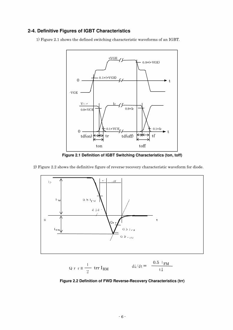
2-4. Definitive Figures of IGBT Characteristics
���-�!�� ��"����� ���� �� ��� ��� ������!�������� ������� �� ������������)/��"�
�
N6/��
"�O�N6/���
"&O)��"&O63��
"�O)��"�O63��
��
)��6��! �
�
������� ���������������
��
���������
"&O�N6/���
�6/��
�Figure 2.1 Definition of IGBT Switching Characteristics (ton, toff)
�
���-�!�� ��"����� ���� �� ������� ���!�� ����� � �� �� ��� �*�������� ������� �� ������������� "�
�
�Figure 2.2 Definition of FWD Reverse-Recovery Characteristics (trr)
"$# %'& %)(*(
+ #-,. " / .10
02
2'3 �4 + #-,
253 4 +25356�+87 ,
9�:;: �+ 7 ,
<>=?=P @
A����)5�
BDC5EFBHGJI "8 K -�GML
7 ,
��7���
3. Precautions for Safe Use 3-1. Derating
��� ���� �)/�������� �� ��������*0��� �� ������ � �������� �����!����� ��� �� "�
2�����!������� ����� ���� �� �� ����� ��� �������� $���� �� � 0��� ��� ������ �����!����������� �
�� �������� ��������������"�
����6����! N ��$������ �1������! ������������ $� ��IM������� �������! �63�;0������� �43������! ������������ $� ��8����'M����63�;"�
2����$������ �1�������� ��*����� �0�63�;������� ��&M��� �1������! ����� �"�
��� %�A� ��<�������������������� ��� ���� �������! �������)/�������� �������!�� ��23���� ������� �
�����! ������ ���� �� �"�
� � � VCES=Vin�2+Vs+Vreg+� �����������
� � � 63�;� D�5�! �������! ����)/�������� �
� � � 6��� D�)����������! ����23���� �
� � � 6�� D�:� ������������! �
� � � 6� !� D�)��� �� �������! �� � �� �� ����� ! � ������"�
� � � Q� � D����!���
���� � 3��� ��%�4����!��� ��� ��*����� ����������0�)/�������� �43����� �������������� $� ��8���� �
'M������ ���� ��43����� ����� � ����� ����� ���� �1����� ��
��$����� ���� � ������� ��*����� �� ������� ���� $� �� &M� ��� �� � ��� �� 43� ���� ��� �� � ����� �
���� ��� � �1� ���� �"� .� � �0� ��� � �����!� ��� �� � =�������� � �� ����� 0� ���� ��� ��� � ��� ��
��������!�*"�
)����������0� ������� �� ���� ��� �)���� ��� �� � �� ��������������� �� � � �1� ���� ��� ���� � ��������!�
� ��� �*� ���� ��� ��� � �R������ ���� �����!�� � �� �� ��� �*���� �� � �� � � ���!����� 0������� �
��� �� �� ���� �� �������� �������!����������� ���� ������������� ��������������"� )������������0� �����
���� � �������� ��� ��� � �� ��*������!� ������� ������������� ������ �������� ���� ������ ������ �� ��
�� �����������*"�
; � ������ ��� �� � ��� �� 43� ���� ��� ���� �� ���� ����� ���� ���� ��� )/��� ����� � ����� ��1 �� �����
��������� �����!������ ������� � ���*�����!��� ������ ��!� <������"�
� � Ip=Pinv×�÷Vac÷�3×�2×�� �����������
� Ic>Ip÷� � ����������
� � � Ip� D�+ �1����� ���� � � Pinv� D�)�� �� ������������ �� � � �� D�:� �������������� � � Vac� D�23������! �� � � �� D�3��� �������� ��������
� � Ic� � D�5�� ��43����� ������)/�������� ����� ������ ��������� ����� �� D�4 �����!��������
��� K�������� � �� ����� %� 4����!� �� � �� ��*����� � ���������0� � �� � IM� ��� �� � ��� �� =��������
� �� ����� ����$��������� ��
��$������������ ��*����� �����������0��� �=��������� �� ����� ��������� ������� ������&M����
�� ���� ����$����"�
� � 3�� � � �� ����� � ������� ���� $� �� ��")�� ��������0� � � ����� � ����! � ��� =��������
� �� ����� � �=� ���� ��� � � �� ����� � ��� ���� �� ��� ��� ��� ��� ����� ������ ��� �� � ����� 0� ����
� � ����!������ ��� <� ���*��� *��� �����! �0������*�� ��� ��� ���� ������ �� ��� 0������ �� �� �
��� ���"�
� � +� �� �� � �����; �������7�C�� �����)�� ���� �����. ���4�����������4 ��!�C������ �����"�

��I���
3-2. Snubber Circuit �� ������ �������������������������� �� ��������� ����� �� ������!�� ��� �� � ���� �� ������!�� ��� ����
���� ��:--��������� ��� ������������! �! � ��� ���*��� �����! �� � �!*������ ���� ���������� "��� � �
�� �! � ����*�� ���*� �%��������������*� ����������!����3�����5��������������*� � ���������� ������ "�
, ������ �)/��0��� ��������*� � ������!�������! ����! ������ ����������� �"�)����������0��� �)/�����*�
� ��� �� ��������� ������ ��������������� ����������������� ���������� ����!� ���*�� ��� �������� �� �1�
���! ������! ������ ��������� �����������IM����� �������� �)/�������� >����$����������!"��
3-2-1. Features of Various Snubber Circuit
� � � � � � � � � � �
O P�QSR$T U�U$V W!XZY[V \Z] ^�QS_`Ra])V b�] WcRDdeP ] f�^ Q�gS_eh�d ] U�] d)_ \ YZf!i[RM] h g!dZY h \efcY)V RD\ P)QaYZX Q f R P�Y Y \DXZY[V \`] ^�Q
i)RM] f[QDj`fcQ Q�klReYm\ P$_ZR;\ W U�QDY j!dc_ f)d T8_ \n_ R�Tc\)_ VZ_ o QZglj`Y fJR p�]$VZV-dZ] U�] dc_e\ WmR _`\ T ]�\c_$Y h[R`q�
rr rr�sat�uwvsat�uwvsat�uwvsat�uwv �
xzyxzyxzyxzy�xzyxzyxzyxzy
�
xzyxzyxzyxzy�
xzyxzyxzyxzy�
{{ {{|yy yy�
{-y{-y{-y{-y�
{-y{-y{-y{-y�{-y{-y{-y{-y
�
}zy}zy}zy}zy�
}zy}zy}zy}zy�
}My}My}My}My�
xwyxwyxwyxwy�
~~ ~~��lt�uwv�lt�uwv�lt�uwv�lt�uwv � ~~ ~~
��'t�uwv�'t�uwv�'t�uwv�'t�uwv �~~ ~~��lt�uwv�lt�uwv�lt�uwv�lt�uwv �
{-y{-y{-y{-y�
}Fy}Fy}Fy}Fy�
}wy}wy}wy}wy�
rr rr��'t'uwv�'t'uwv�'t'uwv�'t'uwv � rr rr
��'t'uwv�'t'uwv�'t'uwv�'t'uwv �
��U U�Q fm] h�gSVeY bcQefc��R _ g�QMf[QcV$] \)_ Y h)Rz�)Q \ebcQ QZhD�[R kD��R k�
OZPcQmR TZU U8V W!X Y[V`\ ]�^ Qm_ R;][V$b ]ZWcRDd P ]Zfc^�Q gm_ hD� Y�\ P�dZ] U ]�dc_ \ZY f)R|� i)R ��]Zh g�d Y�h \`f Y[V`R�\ P)Q�Y X�Q f R$P Y�Y \�X Y8V \`] ^ Q
O P8_ RD\ WZUcQ;Y j!dc_$fcd T*_ \m_ RMT)\c_ VZ_ oZQ g!j Y f�V$] f[^ZQ�d ] U�] d)_ \ WnR _e\ T�] \c_eY h)R q
�
]c\DQ ]�d Pm] fZp[RZq�
i P ]Zfc^ZQ|]Zh g!gc_ZR d P�] f�^ QD] f)Q-f�Q U[Q`] \�Q gDY h!Q X�Q f�W�Reb$_`\ d P8_ h ^;Y�j|QZ] dePS]`f pnj f�Y p!� �n\ YnR$T U U8V W
�
�cQ X�Q f8R Q;�$_$]cR QZga��] j�Qa�`UcQ`f ] \)_ YZha��fcQ ]'� �Z� � �e�[��
X Y)V \Z] ^ Q�qM�cQ dZ] T8R QD\ PcQ!R`h T ���cQefMV$YcRm_ RmV ]`fc^�Q k�\ P$_`RDdc_ f)d T8_ \n_ RM�cQ�R \!R T*_ \ Q�gD\ YDh ] fZf YZb
�g Q X)_ d�Qa]�h gMbcY`T$V g�k!^ Q h�Q f�][V kDhZYc\M�cQ;T[RZQ gMbe_e\ P�� � �ZO!p Y g`T$VeQ R q
� �Figure 3.1 Features of Various Snubber Circuits.
�
3-2-2. Snubber Circuit Operation
-�!�� �"��� �� � ������������������� ��� ������! ������� �� ���� �����������������)/�������� ���� �
���������!�:--"�-�!�� �"�� �� � ������� <����� ���������������������� ������� ������ ���� ���� "�
�3��� �������� � ���� ������� ����#�������� ���� ���$����������� �������
5�5�5�5�
#��#��#��#��#��#��#��#��#��#��#��#��
#��#��#��#����������
�������� �� ��3333
�� �� �� ��-,4-,4-,4-,4
-, 4-, 4-, 4-, 4
-, 4-, 4-, 4-, 4
)/��)/��)/��)/��
)/��)/��)/��)/��
)/��)/��)/��)/��
3�3�3�3�3�3�3�3�
#:24#:24#:24#:24
5�5�5�5� 4�4�4�4�4�4�4�4�
)/�������� ���� ����������!���� )/����������������*
��
;���� ��3�������� � ��+������� � � � � +�������;���� ��3�������� � ��+������� � � � � +�������;���� ��3�������� � ��2����
Figure 3.3 Equivalent Circuit in a Transient State in Fig.3.2 Figure 3.2 Turn-OFF Mode of Bottom Arm IGBT�
��&���
� � -�!�� �"�� �� � ��������! ������� ����� �������� � ���� ��������)/��0� ����� ���:�0�������� ��
:--"�, � ���� ������������)/���������� �����0��� ���������� ������� �������!���� �-, 4������ ���������
�������� ���$ �"�4������! ���� � �!*���������� �����#����������� ������� ������������)/���������
�� ������! ������� ������ ���� �� ����������� ���������� ������ ����������� ������������������! �
� ���������"�
� � -�!�� �"���� ����������������!�������� ����������� ���������#��� � �!*�������!������!���� ������ ��
������������� ��!�� ���$ �"���������� ���� ������! ������ �����"�.� � �0����� ����*0��� ������ ����������
��������� ����!���������� �#��� �������*����� ��� ������! "�.� �����#�������#���� �� ��� �S��� �
��� ������������� ��� ���!��������� �������������*��� � ��������������� �*"��
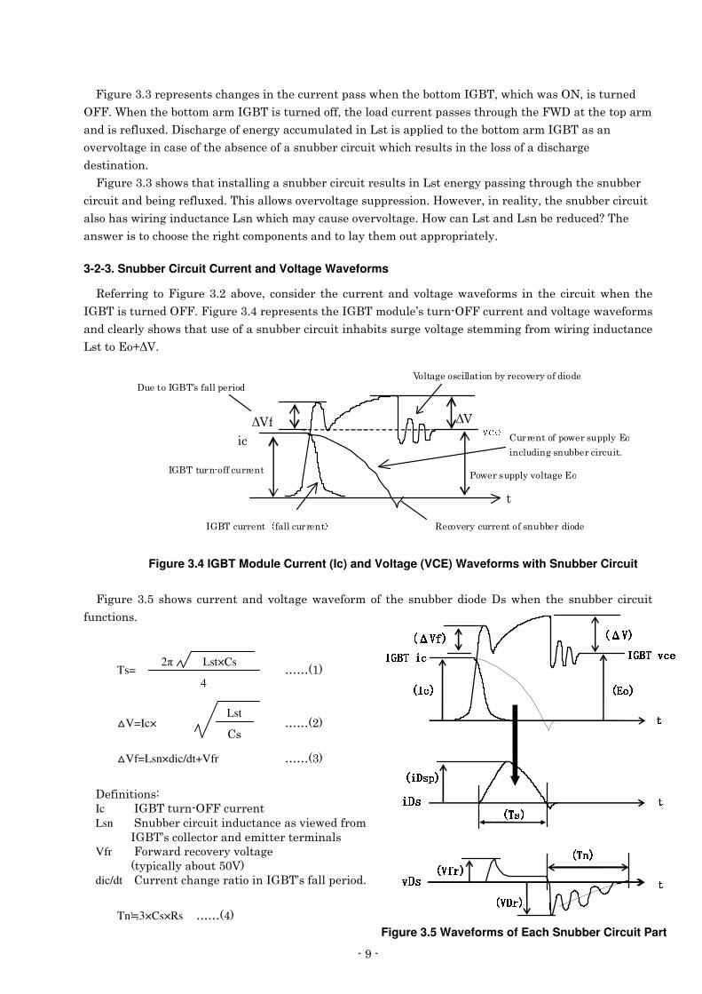
3-2-3. Snubber Circuit Current and Voltage Waveforms
5 � ����!����-�!�� �"������ 0������� �� �� � ���� ������������! � �� ��������� �� � �������� � �� �� �
)/���������� ��:--"�-�!�� �"(�� �� � ������ �)/�������� G�������:--����� ������������! � �� ������
������ ���*���� ��������� ����������� ����������������������! ������! ��� ����!������ ����!���������� �
#��������NT6"�
4� ����)/��G�������� ����6����! ��������������*�� ��� �*��������
3��� �������� �������*���
)/���������������� ��
)/������� �� � ��������� �� � 5 ��� �*����� ����������� ������
�S�l�T6
���
T6�
+� �������*������! ���
�
��������!������ ���������"
�
Figure 3.4 IGBT Module Current (Ic) and Voltage (VCE) Waveforms with Snubber Circuit
-�!�� �"8� ��� �� ���� ������������! � �� �������� �� � ����� ������ �4�� � �� �� � ����� �� ��������
���������"�
�
�
Ts= � U U ����
�
�
�V=Ic× � U U ����
�
�Vf=Lsn×dic/dt+Vfr� � U U ���
�
4 ���������%�Ic � )/��������:--����� ���Lsn� ;���� ������������������� ������ �������
)/��G������ ��������� ���� ��� ��������Vfr� -�� ����� ��� �*������! �
��*������*�������86��dic/dt� 3��� �������! ����������)/��G�������� ����"�
�
Tn�3×Cs×Rs� U U �(��Figure 3.5 Waveforms of Each Snubber Circuit Part
Lst
3��
2� Lst×Cs
4
�
�� ��
�� ��
���-�|���l a¡���-�|���l a¡���-�|���l a¡���-�|���l a¡¢¢ ¢¢l££ ££�¤l¥¤l¥¤l¥¤l¥
���-�|�§¦' ���-�|�§¦' ���-�|�§¦' ���-�|�§¦' ¢ �5 ¥¢ �5 ¥¢ �5 ¥¢ �5 ¥
¢¢ ¢¢l££ ££¨¤l©a¥¤l©a¥¤l©a¥¤l©a¥
�� ��
¢ ¦�ªS«5¬ ¥¢ ¦�ªS«5¬ ¥¢ ¦�ªS«5¬ ¥¢ ¦�ªS«5¬ ¥¢ �H« ¥¢ �H« ¥¢ �H« ¥¢ �H« ¥
¢$¤ ªa ¥¢$¤ ªa ¥¢$¤ ªa ¥¢$¤ ªa ¥¢e¤l© ¥¢e¤l© ¥¢e¤l© ¥¢e¤l© ¥
¢ �|® ¥¢ �|® ¥¢ �|® ¥¢ �|® ¥
¯5°!±¯5°!±¯5°!±¯5°!±
² °!±² °!±² °!±² °!±
¢e³l´a¥¢e³l´a¥¢e³l´a¥¢e³l´a¥
������
)����������0��� ����� ���� ��������� ��� ������� ���� �� <��� ������������! �&8M���� �� ��� �����! �
�����! ����3����������$���� ������!� <��������(�"�. � 0�5�������� �� ����������� �������������N��E�L��"�
��� � %� )���� ����� � <�������������� ���� ��������� ����� ��������0��� ����� ������������<�����������
������ ��������� ���*�V�0������� ��6���������<����������������� ��������� ���*��LV�"��
3-2-4. Collector Current Class and Snubber Capacitor Values
�� ������ ��������������������3������ ������ ��������� ������!��� ������ ��!� <��������������!�)����
� ������!����� �����$��������� ����������! �!�������T6"�
�
� 3� � #�� µ �� � � ¶ � U U U �8���� ·
-���������� �����������0��� ������* �� �� ����������������������������������� ����!���� �� <� ��*�
������� �������"�·��� ����������� ����������>��� ��� �� ��������0���!��� �� ����� ����*����� ��� ��������! L�������! �
���� ��"�
�
3-2-5. Snubber Resistance Selection
�� �� ����������� ����� ����������!������������������ ������� �)/��G��������!��� <� ��*"�
� � , � ��6����! �T6��� �����! ������� ������ ������� �0�W;��! � ��� �� � ���� ����� ��� )���� ���� ��
:--�� ��� �0���������!������ � <��������'�%��
� W;� ¸ "8O3�OT6 ¶ � U U U �'���
�<��������7��������� �� ����� ������� ����� ������� � � � �� �� ����� � ������������������ �� � ���� �����
���� ������)/��������:�"�
�
� 5����� U U U �7��
�
� � � �#�������� ���������� ������ ������ �� ����!"�
2���0�� �� �� ������$��������� ������ �5��� ��� ����� ������� �����������! ��� �T6��� �����! ����
3�0� ¹ 4 � ������������ ���� <� ��*0��� �3�������! �T6��������� ��������*��������! ��"��
3-2-6. Snubber Diode Selection
; � ���������� ������ ������!��� ���� ������������ �)/��G����� ������ ����� ���� �������! ����� "�A� �
���)/�������� � ���������� ��������!�����L������L8����������� �)/����� �"�
A� ����� �� ������!���� ���� �����������"���� ����������� �� � �� �� ��� �*�������� ��������� ������� �
�������� ��� �*����� 0���!���� <� ��*���������������*������� �������� ����������! ����)/��������:--"� �
�
�
)�
T6�
#���
3��
�������
Figure 3.7 Gate Charge (QG) Characteristics
! � � ���� �������! �6/��
!�� � � ����������! �H/�
��%�������� �� ��� � ������3� �
3�%����� �� � ������� ���� ����3� ������3� �
2�%����� �� � ������3� �
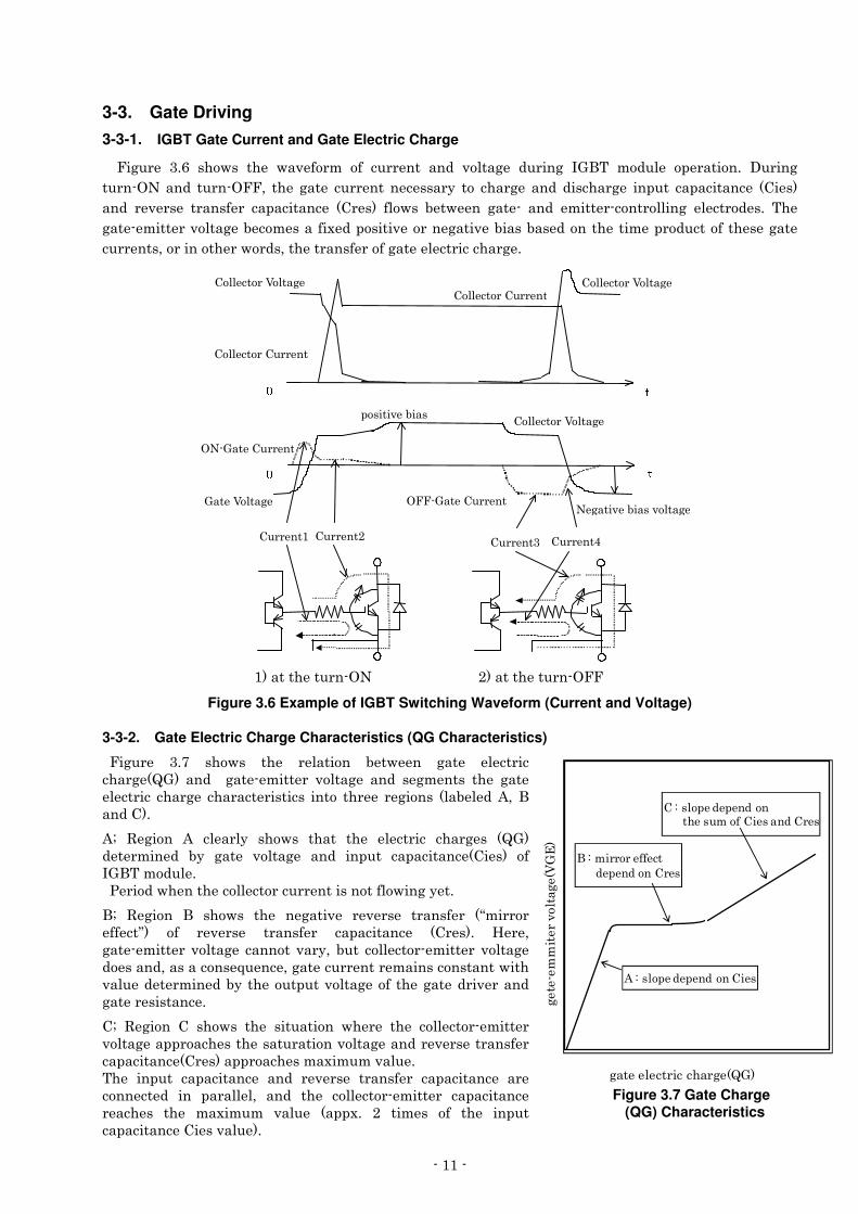
3-3. Gate Driving 3-3-1. IGBT Gate Current and Gate Electric Charge
� � -�!�� � "'� ��� �� �� � �� ����� ��� ���� ��� ���� �����! � �����!� )/��� ����� � �� ������"� 4����!������:������ �����:--0� �� �!�� � ���� ���� � ����*� ��� ����! ����� �������! ������� ���������� � �3� ���
���� � � �� � ������ �� ���������� � �3� ��� ��� �� � � �� !�� �� ���� ���� ������������!� � ����� �"� �� �
!�� � ���� �������! �� ��� ������$ ��������� ����� !���� ��������� ������� ���� �������������� � �!�� �
���� ���0���������� �� ����0��� ������� �����!�� � � ����������! "��
�
�
�
�
�
�
�
�
�
�
�
�
�
�
�
�
�
�
� � �������� ������:�� � � � �������� ������:--� �
Figure 3.6 Example of IGBT Switching Waveform (Current and Voltage)
3-3-2. Gate Electric Charge Characteristics (QG Characteristics)� �
� -�!�� � "7� ��� �� �� � � ������� � � �� !�� � � ����������! �H/�� ��� !�� � ���� �� �����! � ���� � !� ���� �� � !�� � � ������ ����! � ������� ������������� ��� �� !����� ���� � ��20�������3�"�
2D� 5 !���� 2� �� ���*� ��� �� ����� �� � � ������ ����! �� �H/��� � ���� �� �*� !�� � �����! � ���� ������ ���������� �3� ��� ���)/�������� "�� + ����� � ���� ����� ��������� ������������� ��!�* �"�
�D� 5 !���� �� ��� �� �� � � !���� � � � �� � ������ �� �X������� �� ��Y�� ��� � � �� � ������ �� ���������� � �3� ��"� . � 0�!�� � ���� �������! � ������� ���*0����� ���� ����� ���� �� �����! ��� �����0���������� <� �� 0�!�� ����� ���� ��������������� �������� �� � ���� ���*��� �������������! ������ �!�� ����� ������!�� �� ������� "�
3D� 5 !���� 3� ��� �� �� � ���������� � � � �� � ���� ����� ���� �������! ��������� ���� �����������������! ������ � �� ������� ������������ �3� ����������� ����$��������� "��� � ������ ���������� � ���� � � �� � ������ �� ���������� � �� ����� �� �� ��� ������ �0� ���� �� � ���� ����� ���� �� ���������� �� ��� �� �� � ��$����� ���� � ����$"� �� ��� �� ��� �� � ���������������� �3� ������ �"�
3��� �����6����! �
3��� �����3��� ��
������� �����
:��/�� �3��� ��
:--�/�� �3��� ��/�� �6����! � !���� �����������!
3��� ��(3��� ��� 3��� ��3��� ���
º»
º»
3��� �����3��� ��3��� �����6����!
3��� �����6����! �
�������
Figure 3.8 Driving Voltage and Gate Charge Characteristics
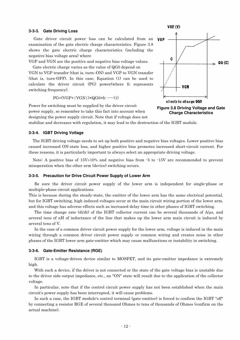
3-3-3. Gate Driving Loss
/�� � ���� �� �������� �� �� ����� ���� � � �������� �� ����� ���
$��������������� �!�� � � ����������! �������� �������"�-�!�� �"I�
��� �� �� � !�� � � ������ ����! � ������� �������� ���������!� �� �
� !���� �����������! ��� ��� � � �
6/+�����6/���� ��� �������� ������ !���� �����������! ����� �"�
/�� � � ����������! ����� ������� ����� ����H/�� � ������
6/�����6/+������� ����������0�����Z:�������6/+����6/�������� ��
������ ��0� �����:--�"� )�� ����� ��� 0� �<������� ���� ���� � � �� �� ���
�������� � �� � ���� �� �������� �+/�� �� �� � � � ��� � �� � ����
� ������!��� <� ��*�"�
+/9�6/+N[6/�[�OH/O������������
+� ������� ������!������� ������� ���*��� ����� ����������
�� �������*0����� � �� �������1 ������������������������ � ��
� ��!���!��� ��� �������*��������"���� ��������������! ��� ������
�������? ������ �� �� �� ����� !�������0������*�� �������� �� ��������������� �)/�������� "�
3-3-4. IGBT Driving Voltage
�� �)/���������!������! �� ������� ����������������� ������ !���� �����������! �"�#� ��������� ������
���� ������ �� ��:������ �����0�������!� ��������� ������������ ������ �� �������������������� ��"�-���
�� � �� �����0������������������*���������������� �*��� � ���������������� �������!������! "�
��� %� 2� ������� � ����� ��� �86\�M����� � !���� � ����� ����� �8� ��� ��86� �� � � ���� �� �� ��� �� � ���
����� ������� � ���� ���� �������� ��� ��� ������!�������"�
3-3-5. Precaution for Drive Circuit Power Supply of Lower Arm
� � ��� � �� � ���� �� �������� �� �� �����*� ��� �� � �� �� ���� ��� ��� � �� ��� ���� ���!� ����� � ���
������� ����� ���������������������"�
��������� ���� ������!��� ��� ��*����� 0��� � ���� ������� ��� ������������ ���� � � ����������� �����0�
��������)/���� ������!0���!������� �������! ������������� �������������� ����!�������������� ��� �����0�
��������������! �������� �� � �� ���������������� �� ��� ��*���� ������� ������ �����)/���� ������!"� ��� � ��� � ����! ���� � ���L���� ��� �� � )/��� ���� ����� ���� ��� ���� � � � � ���� ���������� ��� 2L]�0�����
� � ����� �������.������������� ���� �� ���� � �������1 ����� �� ��� ����������� ���������������� ���*�
� � ����� ������6"�)���� ���� ����������������� ������������ �������*������� ��� �����0������! ��������� ������� ������
����!� �����!���� ������� ���� �� �������� �� �� �����*���� ������� ����!����� �� �� �� ���� � ��� ��� ��
���� ������� �)/����� ������!�� � ���� �� �������*����� ���������������������������*����� ������!"�
3-3-6. Gate-Emitter Resistance (RGE)
)/�������� �����! ����� ��� ��� � �������� ����:;-��0���������!�� � ���� ����� ���� ���� $�� � �*�
��!�"� �, ������������ ��� 0������ ����� ������������� �� ������� ����� ������ �!�� ������! ���������������� ��� �
����� ����� ����� ����������� ���� 0� ��"0����C:�C����� � ����� ������� ������ ������������������ ����� �����
�����! "�
)������������0���� ����������� ������������������� �������*���������� �� �������� �� � ���� ������
�������>���� �������*������ ����� ����� �0���� �������� ������ ��"�
)������������ 0��� �)/�������� >����������� ��������!�� � ���� ���������� ��������������� �)/���C���C�
�*����� ����!���� �������5/������ � �������������:�� ������ �������������������:�� ���������������� �
������������� �"�
¼D½D¾�¿`¼aÀ¼D½D¾�¿`¼aÀ¼D½D¾�¿`¼aÀ¼D½D¾�¿`¼aÀ
ÁÁ ÁÁ  ½Ã¿`ÄaÀ ½Ã¿`ÄaÀ ½Ã¿`ÄaÀ ½Ã¿`ÄaÀ
¼D½;żD½;żD½;żD½;Å
ÆJÇ8Æ-È'É-ÊlË[ÈÌÈ|ÍaÎMÊ)Ï5ÆÑÐlÒaÓÆJÇ8Æ-È'É-ÊlË[ÈÌÈ|ÍaÎMÊ)Ï5ÆÑÐlÒaÓÆJÇ8Æ-È'É-ÊlË[ÈÌÈ|ÍaÎMÊ)Ï5ÆÑÐlÒaÓÆJÇ8Æ-È'É-ÊlË[ÈÌÈ|ÍaÎMÊ)Ï5ÆÑÐlÒaÓ
¼D½DÔ¼D½DÔ¼D½DÔ¼D½DÔ
������
, � ������ ����!����5/�0� �������������� �� �� ������ �������*������! ������ ����� ����������� ����
����������� �������������� ���� ��"� )����������0� ��������� ����� �� �� ����/�� ������ ��6����! ��� � ���
�����! ������ ����!�� �� ������� �5/"�
�
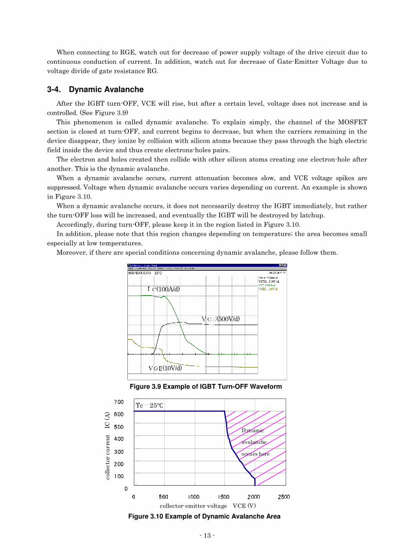
3-4. Dynamic Avalanche
2�� ���� �)/��������:--0�63�� ������� 0�������� ����� ������� � �0������! ��� ���������� �� ��������
�������� �"��; �-�!�� �"&������� �� ��� ���� ��� ���� �� �*������ �������� "� ��� $������ �����*0� �� � ����� �� ��� �� � �:;-���
� ������������� ����������:--0��������� ���� !�������� �� �� 0����� � ���� ������ ���� ������!������ �
� ��� ������� ��0��� *�����? ��*����������� ������������������� ���� ��� *�����������!���� ���!�� � ������
�� �������� ��� �� ��� ������������ �� � � ���������� �������"��� � � ������������� ���� �� ���� �������� � ������� ������������������ ����!��� � � ��������� ���� ��
����� �"����������� ��*�������������� "�,� �� �� �*������ �������� � ������0� ���� ��� ��� �������� � ��� �� ��� 0� ���� 63�� �����! � ���1 �� �� �
����� �� �"�6����! � � ���*�������������� ������������ ��� � ����!�������� ��"�2�� $���� ������� ��
���-�!�� �"�"�, � �����*�������������� �������0������ ������� � ������*�� ����*��� �)/������ ���� �*0��������� ��
�� ������:--������ ����� ����� �� �0����� � ������*��� �)/��� ����� �� ����* ���*��������"�2�������!�*0������!������:--0��� �� �1 ���������� �� !�������� �����-�!�� �"�"�)����������0��� �� ���� ������������ !��������! ��� � ����!����� �� ����� D��� ��� ��� ��� ��������
�� �����*������ �� �� ����� �"���� �� �0������ � ��� ��� �������������������� ����!��*�������������� 0��� �� ������ ��� � "�
� �
�
�
�
�
�
�
�
�
�
�
�
Õ×Ö��2L���
ØÙÖÑÚ�86L���
�Û�ÜÑÝ ��6L���
Þ�
ß5Þ�Þ�
àaÞ�Þ�
á|Þ�Þ�
â|Þ�Þ�
ã Þ�Þ�
äaÞ�Þ�
å Þ�Þ�
Þ�
ã Þ�Þ�
ß)Þ�Þ�Þ�
ß ã Þ�Þ�
àaÞ�Þ�Þ�
à ã Þ�Þ�
���� ����� ���� �������! � � 63���6��
���� ��������� ����)3��2��
4*������
�������� �
�������� � �
�
�� ¸ �8��Figure 3.9 Example of IGBT Turn-OFF Waveform
�
Figure 3.10 Example of Dynamic Avalanche Area
�
���(���
3-5. Parallel Connections
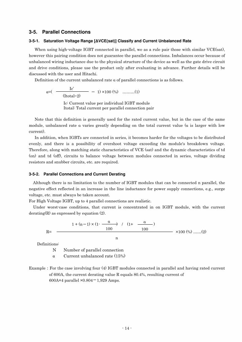
3-5-1. Saturation Voltage Range [�VCE(sat)] Classify and Current Unbalanced Rate
,� ������!���!�������! �)/������� �� ����������� �0� ��������� ���������� � ������� �����63������0�
�� � �������������!������������� ������!������ ��� ������� ������ ������"�)������� ��������� ���� ����
�������� �� ����!���������� ��� ������ ���*�������������� ������ �� ��� ���� �������� �!�� ����� ���������
�������� �����������0��� �� ��� ��� ������������*���� �� ��������!� ��������� "�-���� ��� ������ ����� �
������� �� ������ ��� ������.������"�
4 �������������� ����� ����������� ����� �Q���������� ������ ������������������ �"�
�
� �9� � æ � ���O���M� U U U ���� �
�)�%�3��� ������� �� �������������)/�������� �
� � )�����%����������� ���� �������� ������ ������������
��� ������������ ��������� ���! � ����*��� �������� ���� ������ ������� 0����� ����� ���� ������ ���� �
����� 0��������� ����� � Q� ���� �� !� ���*�� � ����!� ����� ����������� ��� ���� � �Q� ��� ���! �� ������ �
���� ���"�
)����������0� � ��)/������ ����� �� ������ �� �0����� ��� ������ �������� ������! ������ ���������� ��
� ��*0� ���� �� � � ��� �� ����������*� ��� �� ������� �����! � $� ���!� �� � ����� >�� �� �1�� �� �����! "�
�� � ��� 0�����!� �����������!��������������� �����������63�������������� ��*������������� ��������������
����� ���� ��� �����0� ��������� ��� ������ � �����! � � � �� ����� �� ���� �� �� ��� � �� �0� �����! � �������!�
� ����������������� ����������0� ��"��� �� <��� �"�
�
3-5-2. Parallel Connections and Current Derating
2�����!���� � ���������� ������������� ����� �����)/�������� ������������ ����� �� ���������� �0��� �
� !���� � �� ���� �� �� ������������ �� ������ ���� ���������� ������� �������*����� ������0� "!"0����! �
�����! 0� ��"�������� �*��� ���1 ���������"�
-���.�!��6����! �)/��0�������(������� ������ ��������� �� �������"�
A�� �� �������� � ����������0� ����� ���� ��� ��� ���� ����� �� ��� ��� )/��� ����� 0� ���� �� � ���� ���
� �����!�5����� $�� �� ���*� <����������"�
� �� � � � � � ��N��� æ ���O���� �� � L� � ��N ���� 59 � � � � � � O���M��U U ����
� � � � � �� � � �
4 ���������%�
� � � � �� ���� ����������� ������ ������
� � � � �� 3��� ����������� ����� ���8M��
�
�$���� ç -����� ���� ���������!�������(��)/�������� ������ �� ����������� �����������!���� ������ ������'20��� ����� ���� �����!����� �5� <�����I"(M0�� ������!����� ������ �
'2O(������� ��O"I( è �0&�&�2���"� �
)�G�
�)�����̂���
Q�
��
Q�
��
���8���
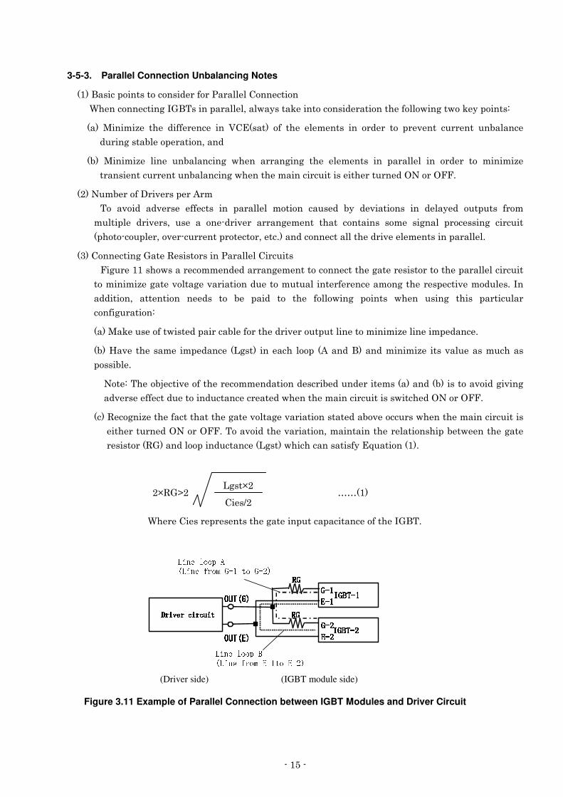
3-5-3. Parallel Connection Unbalancing Notes
�������������������������� ������+����� ��3��� ����� ,� ������ ����!�)/������������� �0��� �*����1 ������������ ��������� ������ ��!�� ��1 *�������%�
���� � ���� �? � �� � ���� � �� � ��� 63������� ��� �� � � � ���� ��� ��� �� ��� �� � ��� ���� ��� �������� �
�����!������ ��� ������0�����
���� � ���� �? � ��� � ����������!� � �� �����!��!� �� � � � ���� ��� ������ �� ��� ��� �� ��� � ���� �? �
������ ������� �������������!� � ���� ����������������� ��� ������ ��:�����:--"�
�������� �����4��� ���� ��2���
��� ������ ��� �� � �� ���� ��� ������ �� ������� ���� �� �*� � ��������� ��� � ��* �� �������� ���� �
������� � ���� ��0� �� � �� �� ����� �� �����! � ��� ����� ��������� ��� � ��!���� ���� ����!� ��������
������������ �0��� ������ ������� ����0� ��"���������� ��������� ����� � � � ������������� �"�
���3��� ����!�/�� �5 �����������+����� ��3������� -�!�� ������� ����� ���� �� �������! � ���������� ����� �!�� �� ������������ ������� ����������
���� ���� �? �!�� ������! ������������� �������������� �� � �� �����!��� �� �� ���� ������ �"�)��
��������0� ��� ������ � ��� ��� � � ����� ��� �� � ����� ��!� ������� � �� ����!� ����� �����������
�����!�������%�
����� �1 ��� ����� ��� ����������� ������� ����� ������������ ����� ���� �? ���� ���� ���� "�
����.�� ��� ���� ���� ���� ��#!���� ��� ��������� �2������������� ���� �? � �������� ������������
������� "�
��� %��� ���= ���� ������ �� ���� ��������� ����� ����� ���� ���������������������������!����!�
��� �� � �� ����� ������������� ��� �� �� � ���� ������������������ ���� ��:�����:--"�
����5 ��!��? ��� ������������� �!�� ������! ��������������� ������ �������� � ���� �����������������
��� ������ ��:�����:--"������������ ����������0������������ �� ������������ � ���� �!�� �
� ��������5/�������������������� ��#!���� ���������������*��<����������"�
� �
� � � � � � �
� � � �O5/F�� � � U U ����
� � � � �
� � ,� � �3� ��� �� � ������ �!�� ����������������� ������ �)/��"�
�
� � � � � �
��
é'êé'êé'êé'ê
é'êé'êé'êé'êëíì5î`ï�ð)ìòñ�îZì�ñ�ó'î�ôëíì5î`ï�ð)ìòñ�îZì�ñ�ó'î�ôëíì5î`ï�ð)ìòñ�îZì�ñ�ó'î�ôëíì5î`ï�ð)ìòñ�îZì�ñ�ó'î�ôêê êêwõõ õõSöö öö
÷÷ ÷÷wõõ õõ-øø øø�
êê êêwõõ õõ-øø øøíù ê�ú5ûù ê�ú5ûù ê�ú5ûù ê�ú5ûwõõ õõ-øø øø÷÷ ÷÷wõõ õõSöö öö ù ê�ú5ûù ê�ú5ûù ê�ú5ûù ê�ú5ûwõõ õõ öö öö
ü|ý)þwÿ����������� ü|ý�þzÿ����� ������������������
��������������������������������������������
������� �!�������� �!�������� �!�������� �!�
ü|ý)þwÿ������!��"� ü|ý�þzÿ����� �#����$�!��#��%�!�
�Figure 3.11 Example of Parallel Connection between IGBT Modules and Driver Circuit
�
�
#!��O��
3� �L��
(Driver side) (IGBT module side)
���'���
3-5-4 && && Necessity for Symmetry of Main Circuit Wiring
����,����!��<����?������
-���)/�������� ������ ����� �� ����������� �0������� �� ������
��� <����? ��� � ����!������ ����� ����������� � ����!������ �
� ��� �� ���� ������� �����1 ����������� ����� ����������� "�
-�!�� �"���� �� � ������� $���� ��������� ������� �� ����!�
������� ������� ���������!��������������� ������������������!�
������������� ����!���������� ���������"�
-��� �� � ���� ����0� ����!� ��������� � �������� #32� ���� #3��
�� � ��� �0� ���� ���� �� � � ��� �0� ����!� ��������� � ���������
#�2�����#��"�
,� �� �� � )/��� �2�� ���� ���� �� � ������!� :�0� �� � ���� ���
! � ��� �� ��� ���� ����������� ��������� � � ���� ��� �� �
����������� ��� �� � ��������� � ��������� ���� �� ����� ��� ����
� � ��G��������� �������"�
� � � ���� � �� � ���� ��� ������ � � � ���� ����������*� ��� �� �
��������� ������0�����������������1 ���*�� ��*���� ����!��*�
�������!��� ���������� ����� �"�
-��� $���� 0�� � ����!�-�!�� �"��0���� ����!���������� ����2���������� ���� ��������� ����������0�
#32N#�2�E�#3�N#���������� �63����������� ����)/���2�� ��� ����� �0��� ���� ����� ���������!� ���
� ���� �����-�!�� �"�� ����� ����"�
)�� ����������0� ��� � ��� �� ��� �� #�2� ���� #��� �� � �������� �0� �� � )/��� !�� � �����! � ���� � �
��� �� �*������ �� �0�������!������������ ������ ��"�
����A������� ��3��� ���+ ��������� ���*�,����!�
� � -�!�� � "�� ��� �� ����� ��� � �� ���� ��� �������� � �������
� �� ������!� :�� ��� )/��0� ��� ���� � � <����? �� �����!� �� �
�� ��*����� � ���������� ��� �� ���������!� �� � )/��0� ������*�
� �����!��� ��������� ��)�2�����)������� � ���� ���*�63������"�
�� ���� �� <��� �������� ��������� ������ ������� � <����? ��
���� � � �������� �� ��� �� � ��� �������� �� �� �� � #�5� ��������
���� �� �*� �� � ��������� � ������ �� � ���� ������� ������!� ��
������ �� �������� ���� �� � �� �����!� � ������� � ��� �� � )/���
� � ��"� �� � �� �����!� � ������� � X���Y� ���� � � ����*�
�������� ������ ��� ��������������� ������������ "�
� � -��� $���� 0��������������������� ������!������!� �
���0����X���Y���������$���� �*�"(�� ���������� � ���=è �8� '�L����� ������ ���� ���� � ��� � ��"� )-��� ������ ��������� � ���
��.� ���� �� ������ �� �����!�������0� �#32N#3�N#�2N#���0�
�� � <����?������ ��� �������� �� ���� ��� ������� ��� �� ��� �� �
��� ����������_���������$���� ���*� <����������"� �
� _ è � è �8 R� U U ����
)���� ���������*������ ����� ��������������������� ������ ����� ��_���������0�������������������$���� 0�
������&8M�0��� ����� ��������� ��������� �� � ���� ���*�63������� ������(8R����� ��������!�:�"������
� ���� ��� �� � ����� �� �� <� ��*� ��� ��!�� ��� �� � ����� � ��� � ��� ����� �0� �� � ���� ��� ������ � ��*� � �
� � ���� ���*��� � ����!����������!��� ����� ��������������� � ��� �� ����"�
�
(!)(!)(!)(!) (�)(�)(�)(�)*�+�,.-�/�+10%,.+20�34,�5*�+�,.-�/�+10%,.+20�34,�5*�+�,.-�/�+10%,.+20�34,�5*�+�,.-�/�+10%,.+20�34,�5
6�7986�7986�7986�798697!:697!:697!:697!:
6�;�86�;�86�;�86�;�86�;�:6�;�:6�;�:6�;�:<< <<>= 3@?4,!A�, B!+�C= 3@?4,!A�, B!+�C= 3@?4,!A�, B!+�C= 3@?4,!A�, B!+�CD/�E�,�5F5!/�+/�E�,�5F5!/�+/�E�,�5F5!/�+/�E�,�5F5!/�+1G4,.+4, H�I!JG4,.+4, H�I!JG4,.+4, H�I!JG4,.+4, H�I!J
KK KK 88 88MLL LLKK KK :: ::NLL LL
OQP�8OQP�8OQP�8OQP�8O�P�:O�P�:O�P�:O�P�:
Figure 3.12 Wiring to Equalize Main Wiring Inductance Values
��.�
"(�`O��
Figure 3.13 Equalization of Unbalanced Current
�
�
,����!� � ����� ��� <����? � #32� ����#3�0�#�2�����#������� <��� �"�
RS�TS�TS�TS�TVUU UU
S�TS�TS�TS�TXWW WWY TY TY TY TZWW WW
Y TY TY TY T UU UU
3��� ��������� ������
����)/��
�
A������� ������ ���A������� ������ ���A������� ������ ���A������� ������ ����9���9���9���9���2��2��2��2�����������������������������
A������� ������ ������A������� ������ ������A������� ������ ������A������� ������ ������������ ��� ��*����� �� � ����� ��� ��*����� �� � ����� ��� ��*����� �� � ����� ��� ��*����� �� � �������������������6� ���� ��������6� ���� ��������6� ���� ��������6� ���� ������������
A������� ������ ��
���7���
�
������ �����/�� �,����!�
� ,� ������!�!�� � ����!���������� �0���� ��� ������ ��!%�
���� ��� ������ ���� � ! � ������� ��� !�� � ����!� ��� ����� �������� ����!� �� � ��� ������� ���������� ���
$� ���� ���� ���������� � �� 0��� ������!����� ����!����1 ���� <��� �������� �� � ������ �"�)��
*���������� ������� �� ����!0������������ ���������� ��� ���� �!�� � ����!"�
����;��� ��� � ��������!����� ���������� � �� �� � ���� ���� �������� ������!�� � �� �0�1 ���� � �
������� ���*������������ ������� �"�
����-����� ���� �������� ������!�� � �� �0���1 � <������ �� �!�������� ��������� ����� ������� �
�� ������ ����!������ ����� ��"��A� �� ��� ������������� ���� �� �!��������� �!�� � �� ����
3-5-5. Dynamic Avalanche and Parallel Connections
�� ��*�������������� ������! � ����� ��������� ���� �� �����! � ��� ��� �� ���-�!�� �"�0� ��� � ��
�� ����������� �������� ��� *������ ��� ����� �����-�!�� �"�0���� ����� ������ ���� ������ ��� ��
�*�������������� ������! "�2�� $���� ������� �����-�!�� �"�("�
-�!�� �"�(������ �� ��������� � ���� � ��� ��������� ��0���������� � ��� ������ ����������0�� ���� �
�� �������������� ������������ �� ������� ������ ���������0���� �� �� �������� ��������� ���������� �������
� ���� � ��� ��������� ��0������������ ������ ���� ������������������ ��� ������!������ ����������! "�
�; �-�!�� �"�8��
)����*���� 0� � ������ �� ����������� �0�� � �� �����*�� �� ������������ ������ �������� ���� ��������
�� �� *������ ��� ����� �����-�!�� �"�"�
�
[�\F]_^a`�b�c�c![edgf%h
i ]kj `ml�c�c�nkd1f%h
[1o ^ `ml�c![edpf%h
i ]rq `ml�c�c�nkd1f%hi ]kj `ml�c�c�nkdgfQhi ]rq `ml�c�c�nkdgfQh
s ]_^ `�b�c�c
���I���
3-6. Calculation of Power Dissipation
����� � ������ �������� �� �� ! � ���������������� ����� �������������� � ������!� )/���� ����� �+,� �
��� �� ���������"�
��� %�2������������������ ���� ��������� ��� �������� ���� �� ����������������� � �� "�
)����������0��� ��� ������������������� �)/�������� � ������������������!������������������� �"�
�������� ��������������9�+� �����������������)/�� ¯ +� �����������������-,4�)/����� ��������������9�;� ��*����� ��� ���������������+����
� � � � � � � � � � � � � � � � � � � � � � � � � � � � � � � N�����:���� ���������������+�����
� � � � � � � � � � � � � � � � � � � � � � � � � � � � � � � N�����:--��� ��������������+����° �-,4��� ��������������9�-�� ������ ���������������+�� ¯ 5 ��� �*��� ���������������+����
�
3-6-1. IGBT Power Dissipation
����;� ��*����� �+� ��4������������+����
63��6�63��6�63��6�63��6�
)�)�)�)�����66663�3�3�3� ������������������9��8��9��8��9��8��9��8 ±± ±±
6666/�/�/�/�9�869�869�869�86
���� ²² ²² ��������
�³´
µ�¶·
� ¸9¸9¸9¸�¸9¸º¹ · »
¸�¸9¸9¸9¸�¸¼¹e½ »¾�¿ À Á Â�ÃÅÄ
� ÆÈÇ ¾9¿ À ÁÊÉ_Ë%ÃÉ Ç Ë%ÃÉ ¶
¶Ì É_Ë_à ¿ ¶
Ì Í ¶ÎÁ
)��2�
)��2�
)��2�
)��2��
·�ÏÐÄÅÑ�Ò1Óµ
·�Ï�Ô Ç Ä�Ñ�Ò1Óµ
4������������:�����*���� ������!���� �� �������
¸9¸�¸9¸9¸�¸Õ¹ µ »
�
�� %�3��� ��������� ������ ��!����)/������������ �������� ��
�� %�;���������������! ���������� �������� ��
)��%�)�� �� ������ ������������ ����������� �
� � <��������� �)/������� ����
�0���%�#��� �������$���� ����� ����� �� �� � �� ��
� �*�63������ è � ¯ � Ö )�� �:������������� �)��63��������� ����������� �����-�!�� �"�'"�� �
���a�%�#������ ���������
���������:��+� ��4��������������������:--�+� ��4�����������
;�������!� ����� �� � ��� �� �� ���� � ���� ��� ���� ���� � ��� )�0� �� �
����������� ���� �1����� �� ��� �� � � �� × )�"��� ��� ��! ����� ����)/�������� ������:������ ������������:--�
���� �����0���������!�����<��������(�0���� )�� �9� � × � 2 × )�� �������(��� ��
49�
)�� ����������� ������� b� �����!� +,� � �������� ��� ������ ��
49 � ��� �������������������� ����*�
)���������� 0�b è ����������� �"��� � �� ��*����� � �� �� ������������ +��� ���� � � ������ �� ����!��<����������
+���9�
2
�
+���9 � ��O��O4�O�c� �
Figure 3.17 Switching Loss vs. Collector Current
Figure 3.16 Ic vs. VCE Characteristic
�
�
���&���
:������ �� � �����:--� �� �� ������������ ���� �����:�� �� �� ������������ ���� �� � ���� � )�� �� ��
���� �������� ���*��� � ��������0�����������-�!�� �"�7�0�� �� ���� �*"�
� � �<��������8�������'������� ��� ������������� ������:���� ��������������+�������������:--��� ��
������������+��������������������������� ���� <� ��*���"���� +��� è ���� × ��������8���� � �
+����è �����× � �������'��
�
3-6-2. Power Dissipation in a Free-Wheeling Diode
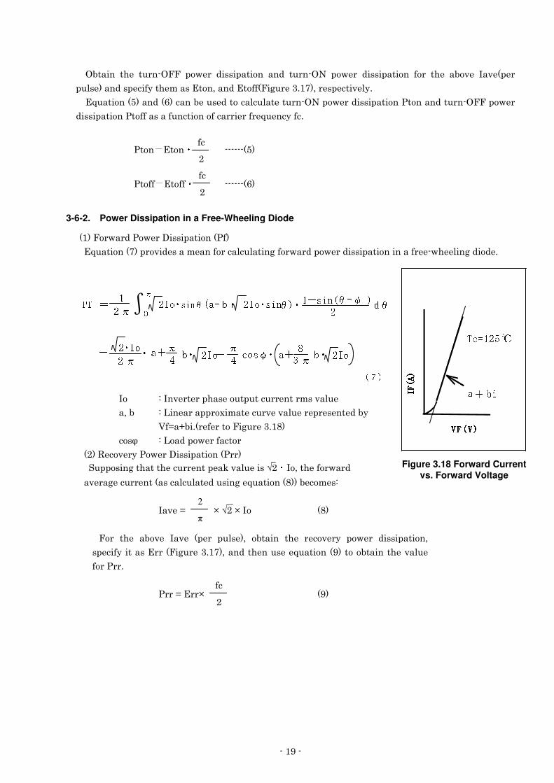
����-�� ����+� ��4������������+���
� �<��������7�������� ����� �����������������!���� ������ ��������������������� � � ���!����� "�
� � � � � �
� � � �
ØkÙ�Ú�ØeÛØkÙ�Ú�ØeÛØkÙ�Ú�ØeÛØkÙ�Ú�ØeÛ
ÜÝÞ ßàÜÝÞ ßàÜÝÞ ßàÜÝÞ ßà
áãâÕäáãâÕäáãâÕäáãâÕäæåèç�éëê�ìåèç�éëê�ìåèç�éëê�ìåèç�éëê�ì
íïî_ðzñ�òeóõô
öV÷ùø�ú
ûü
üý9þ
ÿ�ÿ�ÿ9ÿ�ÿ�ÿ������
ÿ�ÿ�ÿ�ÿ9ÿ�ÿ������
ÿ�ÿ�ÿ�ÿ9ÿ�ÿ�����
ò�� ò ��
��� ò�������� ú���� � ö�� ø! ò�������� ú�� �#"$ %&�' ñ�()� ú��*� � �,+-"
� ö ÷ ø* ( î.�/� + � ö ÷ ø& ò0���ò1�����ò!�
� 2 �� � 2 3!�4 ��
� )�� %�)�� �� ������ ������������ ����������� �
� �0��� %�#�� ��������$���� ����� ����� �� �� � �� ���*�
� � 6�9�N��"�� � �����-�!�� �"�I��
� ���a� %�#������ ���������
� ����5 ��� �*�+� ��4������������+����
;�������!�������� ����� ���� �1����� ����V� 5 )�0��� ���� ����� �� ��! ����� ��������������� ������!� <��������I���� ��� �%�
�
� � )�� �9� � O�V��O�)�� � �I��
�
-��� �� � ���� � )�� � �� �� ���� �0� ������� �� � � ��� �*� �� �� �����������0�
�� ���*������������-�!�� �"�7�0������� ���� � <��������&�������������� ����� �
����+��"�
�
� � +���9����O� � � �&��
Figure 3.18 Forward Current vs. Forward Voltage
���
��
���
��
2
�
���
��
6�798;:<�=�
�
������
3-7. Thermal Impedance and Heat Dissipation Design
3-7-1. Thermal Impedance����
�� �������� ���� �� � ��=��������������� ��5���=��������)/����������� ����� ������ ������� �� ��� �
�� ����������"�
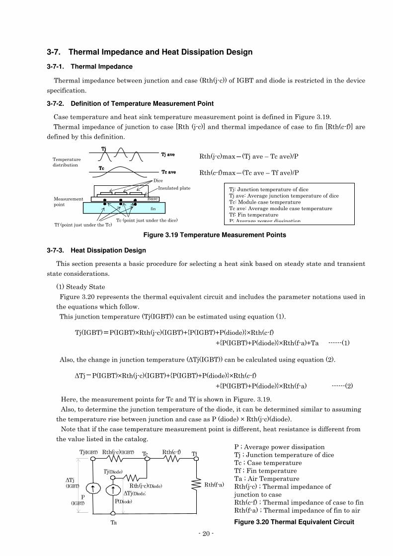
3-7-2. Definition of Temperature Measurement Point
3�� �� �� ����� ������ ������1�� �� ����� �� ���� � ������������� ��� �����-�!�� �"�&"�� � �� �������� ���� ����=�������������� �d5����=���e������� �������� ���� ������� ��������d5�������e��� �
� ��� ���*������� ��������" �
�
�
�
�
�
�
�
3-7-3. Heat Dissipation Design
������ �������� � ���������������� ��� ������ � ����!���� ������1���� ������� ��*����� ����������� ���
���� ������� �������"�
����;� ��*�;��� �
� -�!�� �"��� �� � ������ ��� ����� <����� ��������������������� ���� ������ � �������������� �����
�� � <�������� ���������� "�
� �����=��������� �� ����� ���=�)/���������� � ������ ������!� <����������"�
� �=�)/��� > +�)/���O5���=����)/���Nf+�)/���N+����� �gO5��������� � Nf+�)/���N+����� �gO5�������N��� ����������
� 2���0��� �����! ����=��������� �� ����� ��T�=�)/���������� ��������� ������!� <����������"�
� T�=> +�)/���O5���=����)/���Nf+�)/���N+����� �gO5��������� � � � � � Nf+�)/���N+����� �gO5�������� � ����������
. � 0��� �� ���� � ������������������������������ �����-�!�� "�"�&"�
2���0����� � ���� ��� �=��������� �� ����� ������ ����� 0��������� �� � ���� ��������������������!�
�� �� �� ����� ���� �� � ��=��������������� ����+������ ��O�5���=�������� �"�
��� ����������� ���� �� �� ����� �� ���� � ���������������� � ��0�� ���� ������� �������� � ������� �
�� ����� ����� ������� �������!"� �+�D�2� ��! ��� ���������������=�D�K��������� �� ����� ������� ����D�3�� �� �� ����� ����D�-���� �� ����� ����D�2���� �� ����� �5���=����D��� �������� ���� ���� � � �=�������������� �5��������D��� �������� ���� ������� ��������5��������D��� �������� ���� ���������������
�
�
Figure 3.20 Thermal Equivalent Circuit
�
����� ����� ����� ����� ����
�=��� �=��� �=��� �=��� ����
������������
�=�=�=�=����
5���=�����$> ��=��� �Z������ �L+��5���������$> ������ �Z������ �L+�
�=%�K��������� �� ����� ������� ��=��� %�2� ��! �=��������� �� ����� ������� ���%�� ���� ���� �� �� ����� ������ %�2� ��! ������ ���� �� �� ����� ���%�-���� �� ����� �+%�2� ��! ��� ��������������
� �� ����� ��������������
� ���� � ���������
4�� �
)������ ������ �
� ��� ������
� ����������=������� ���� ����� ��
� ����������=������� ���� ���� �� ��
Figure 3.19 Temperature Measurement Points ���� ����
�� 5���=����)/���
��
T�=��)/���
�=�)/��� 5�������
5�������
�� ��
�=�4��� �
+�4��� �+
�)/���
5���=����4��� �T�=�4��� �
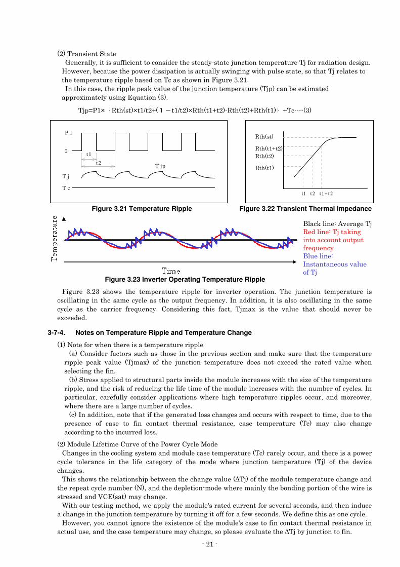
�������
���������� ���;��� �� / � ����*0�������������� ������������ ���� ��� ��*����� �=��������� �� ����� ��=���������������� ��!�"�.� � �0�� ���� ��� ��� ������������������������*�� ��!��!� �������� ����� 0����������=�� ��� ������� �� �� ����� ������ ���� �������������� �����-�!�� �"��"�� )���������� 0000��� ������ �� �1����� ������ �=��������� �� ����� ���=�������� � ������ �������$���� �*�����!��<���������"�
�=�9+�O ? 5������O��L��N� @BA ��L���O5�����N����5������N5������ C N���������
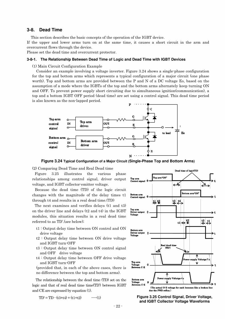
t1
t2
P 1
0
T c
T j
T jp
R th( DFE )
R th(t1+ t 2)R th(t2)
R th(t1)
t1 t2 t1+ t 2
5������
5�����N���5������
5������
� Figure 3.21 Temperature Ripple Figure 3.22 Transient Thermal Impedance �
�
�
�
�
�
Figure 3.23 Inverter Operating Temperature Ripple����
-�!�� � "�� ��� �� �� � � �� ����� � ����� � ���� ��� �� �� �� ������"� �� � =�������� � �� ����� � �������������!������ ���� ��*�� ������ ���������� <� ��*"�)����������0����������������������!������ ���� ��*�� � ��� �� � ����� �� �� <� ��*"� 3����� ���!� ����� ����0� �=��$� ��� �� � ���� � ����� ������� � � �� � � $� � �"�
3-7-4. Notes on Temperature Ripple and Temperature Change
������� ����� � ���� � ������� �� ����� ������ �����3����� ���������������������� ������ ��� ������� ������������1 ���� ������ �� � � �� ����� ������ � � �1� ���� � ��=��$�� ��� �� � =�������� � �� ����� � �� �� ���� $� �� �� � ��� �� ���� � � ��� � ����!��� ����"�����;�� �������� ��������������������������� ��� ������ ����� �� �� ������ ���? ������ �� �� ����� ������ 0������� ����1����� �����!��� ���� ���� ������ ������ ����� �� �� ������ ����� ������*�� �"�)������������0� ��� ����*� ������ �� ������������� � � ���!�� � �� ����� ������ �� �����0� ������� �� �0� � � ��� � ��� ������! ����� ������*�� �"�����)����������0���� ����������� �! � ��� �����������! ������������� ����� �� ��������� 0��� ������ ��� � �� � ��� ��� � ��� ���� �������� �� ����� � ������� 0� ��� � � �� ����� � ����� ��*� ����� ����! ���������!������ ������� ������"�
����� ���� �#�� ��� �3��� ������ �+� ��3*�� �� �� �3���! ������� �������!��*�� � ���������� ���� �� �� ����� ��������� �*������0������� � �������� ���*�� � ��� ���� � ��� �� � ��� � ��� !��*� ��� �� � ��� � � � � =�������� � �� ����� � ��=�� ��� �� � � ��� �����! �"��������� ���� �� ������������ � ���� �����! ����� ��T�=������� ������ �� �� ����� �����! ������� �� � ����*�� ����� �����0������� �� �� �������� � � � ������*��� �������!�������������� � �� ������� �� ������63���������*�����! "�, ��������� ����!�� ����0� �����*��� ������ >����� ������ �������� � ����� �����0������� ������� �������! ������ �=��������� �� ����� ��*�������!��������������� �� �����"�, �� ��� ����������� ��*�� "�.� � �0�*�����������!��� ��� � $��� �� ������ ������ >����� ������������������ ������ ������� ������������� 0������� ���� �� �� ����� ���*�����! 0������ �� � ������ ��� �T�=��*�=��������������"�
����1���� %�2� ��! ��=�5 ����� %��=���1��!����������������������� <� ��*���� ���� %�)�������� �������� �����=� ��
�������
3-8. Dead Time
������ ������� ����� ���� ����������� ��������� ��� ������������ �)/���� ��� "�)�� �� � ��� �� ���� �� �� ����� ����� ��� ��� �� � ��� � ��� 0� ��� ���� �� �� ������ �������� ��� �� � ���� ������ ����� ������ �������!���� �� ��� "�+� �� �� ���� �� ������ ������� ����� ������� ����"�
3-8-1. The Relationship Between Dead Time of Logic and Dead Time with IGBT Devices
����� ����3�������3����!���������$���� �3����� ����� $���� ���������!��������! ���� �� �"�-�!�� �"�(���� �������!� ����� ������!��������
������ ��������������� ������ ������ �� � �������*�����������!���������������=�������������� ����� � �����"��������������� �������� ������� ��� � ���� �+������������43������! ���0���� ����� �� �������������������� � � � ��� �)/��������� ����������� ������� ��������� ���� �*�1 ��������!�:������:--"������ � ����� �������*����������������!��� ������������ �����!���������������������0������������������� �)/���:--�� ������� ������ ���� �� ������!�������������!���"������� ������ �� �������������1�� ������� ��������� ��� ����"�
���������������������������� ����� ����� ����� ����� �
����������������������������
��!�����!�����!�����!���
������ ���������� ���������� ���������� ���� ����� ����� ����� ����� �
:A�:A�:A�:A�)�)�)�)�
:A�:A�:A�:A�)�)�)�)�
3333
++++
////
GG GG���������������������������� ��������
////
���� HH HH����
��������������������������������
������ ���������� ���������� ���������� ����
��!�����!�����!�����!���
����������������������������
�Figure 3.24 Typical Configuration of a Major Circuit (Single-Phase Top and Bottom Arms)
����3�������!�4 ������ �����5 ���4 ������ �
-�!�� � "�8� ��������� �� �� � �������� ���� �
� ������������ ����!� �������� ��!���0� ���� �� �������
�����! 0�����)/������� ����� ���� �������! "�
� ���� � �� � � ��� ��� � ��4�� ��� �� � ��!��� ��������
����! �� ���� �� � ��!����� � ��� �� � � ��*� ��� �� ���
�����!���(������ ������������ ���� ������ "��4��
�� � � $�� $���� �� ����� ���� �� � ��*�� ���� ���� ���
����� ����� ����� ������ ��*�����������(������� �)/���
����� �0� ����� ���������� � ������ ��� �� � ��� � ��� ��� �
� � �� ���������4G"�� �� �� �D�
���%�:������� ��*���� �� � ��:��������������:������ ������! �
���%�:������ � ��*� ��� � � � ��:�� ���� ������! �����)/��������:--�
��%�:������� ��*���� �� � ��:������������!��������:--� � ���� ������! �
�(�%�:������� ��*���� �� � ��:--����� ������! �����)/��������:--�
������� ������0���� ��������� ����� ���� �0��� � ����������� � �� �� � ���� ��������������� ������"�
�� �� ������������ � ���� �� ������ ���4��� ������� �
��!���������������� ���� ������ ���� ��4G��� � ��)/���
����3���� � $�� �� ���*� <����������"�
�4>�9��4�����N�(��N����N���� ���������
����������������������������� ����3���������!���3���������!���3���������!���3���������!�������
������������������������ ���������������� ����3���������!���3���������!���3���������!���3���������!�������
���������������������������� ����4��� ��������4��� ��������4��� ��������4��� ������������6����! 6����! 6����! 6����! ����
������������������������ ���������������� ����4��� ��������4��� ��������4��� ��������4��� ������������6����! 6����! 6����! 6����! ����
���������������������������� ����6����! 6����! 6����! 6����! ����� � �� � �� � �� � �����3333������������
������������������������ ���������������� ����6����! 6����! 6����! 6����! ����� � �� � �� � �� � �����3333������������
4 ������ ������!��4 ������ ������!��4 ������ ������!��4 ������ ������!�������4�4�4�4��������
5 ���� ������ 5 ���� ������ 5 ���� ������ 5 ���� ������ ���������4�4�4�4h�h�h�h�����
����
���������������������������� XXXX:�:�:�:�YYYY����
������������������������ ������� X:�Y���X:�Y���X:�Y���X:�Y
II IIJJ JJ
II IIJJ JJ������������
II IIJJ JJ
II IIJJ JJ
II IIJJ JJ
JJ JJ II II
�(�(�(�(��������
KMLKMLKMLKML
������������
������������
������������
������������
+� �������*�6�����! +� �������*�6�����! +� �������*�6�����! +� �������*�6�����! NN NN ��������
+� �������*�6�����! +� �������*�6�����! +� �������*�6�����! +� �������*�6�����! NN NN ��������OO OO�� ��������:�� ��������:�� ��������:�� ��������:�����������! ����� ����� ��� ����1 ������1 ����� ��������! ����� ����� ��� ����1 ������1 ����� ��������! ����� ����� ��� ����1 ������1 ����� ��������! ����� ����� ��� ����1 ������1 ����� �
�� ��� �-, 4�� ���$"�� ��� �-, 4�� ���$"�� ��� �-, 4�� ���$"�� ��� �-, 4�� ���$" PP PP ����
������������
Figure 3.25 Control Signal, Driver Voltage, and IGBT Collector Voltage Waveforms
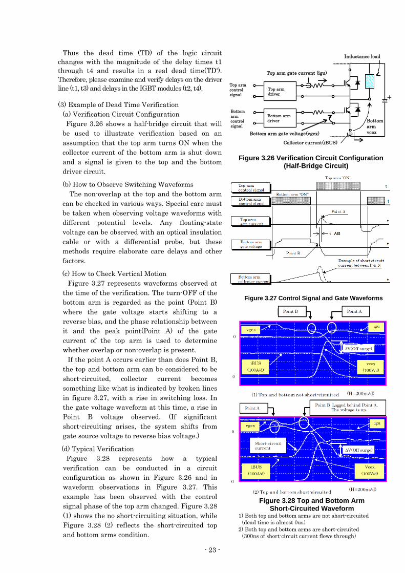
- 23 -
Thus the dead time (TD) of the logic circuit
changes with the magnitude of the delay times t1
through t4 and results in a real dead time(TD').
Therefore, please examine and verify delays on the driver
line (t1, t3) and delays in the IGBT modules (t2, t4).
(3) Example of Dead Time Verification
(a) Verification Circuit Configuration
Figure 3.26 shows a half-bridge circuit that will
be used to illustrate verification based on an
assumption that the top arm turns ON when the
collector current of the bottom arm is shut down
and a signal is given to the top and the bottom
driver circuit.
(b) How to Observe Switching Waveforms
The non-overlap at the top and the bottom arm
can be checked in various ways. Special care must
be taken when observing voltage waveforms with
different potential levels. Any floating-state
voltage can be observed with an optical insulation
cable or with a differential probe, but these
methods require elaborate care delays and other
factors.
(c) How to Check Vertical Motion
Figure 3.27 represents waveforms observed at
the time of the verification. The turn-OFF of the
bottom arm is regarded as the point (Point B)
where the gate voltage starts shifting to a
reverse bias, and the phase relationship between
it and the peak point(Point A) of the gate
current of the top arm is used to determine
whether overlap or non-overlap is present.
If the point A occurs earlier than does Point B,
the top and bottom arm can be considered to be
short-circuited, collector current becomes
something like what is indicated by broken lines
in figure 3.27, with a rise in switching loss. In
the gate voltage waveform at this time, a rise in
Point B voltage observed. (If significant
short-circuiting arises, the system shifts from
gate source voltage to reverse bias voltage.)
(d) Typical Verification
Figure 3.28 represents how a typical
verification can be conducted in a circuit
configuration as shown in Figure 3.26 and in
waveform observations in Figure 3.27. This
example has been observed with the control
signal phase of the top arm changed. Figure 3.28
(1) shows the no short-circuiting situation, while
Figure 3.28 (2) reflects the short-circuited top
and bottom arms condition.
Figure 3.26 Verification Circuit Configuration (Half-Bridge Circuit)
Top arm
driver
Top arm
control
signal
Bottom arm
driver
Bottom
arm
control
signal
+
Inductance load
Top arm gate current (igu)
Collector current(iBUS)
Bottom
arm
vcex Bottom arm gate voltage(vgex)
上アーム「オン」信号
下アーム「オン」信号
t
ポイントA
ポイントB
PN間短絡電流の例
t AB
上アーム制御信号
下アーム制御信号
上アームゲート電流
下アームゲート電圧
下アームコレクタ電流
t
t
t
t
Top armcontrol signal
Bottom armcontrol signal
Top armgate current
Bottom armgate voltage
Bottom armcollector current
Point B
Point A
Top arm “ON”
Bottom arm “ON”
Example of short circuitcurrent between P & N
(H=200ns/d)
iBUS
(100A/d)
vcex
(100V/d)
igu vgex
ポイントAポイントB
ΔV(オフサージ)
0
0
(1)上下短絡していない状態
0
(2)上下短絡している状態
iBUS
(100A/d)
Vcex
(100V/d)
igu vgex
ポイントB(Aよりも位相が
遅れ、電圧値も上昇する)
0
短絡電流
(H=200ns/d)
ΔV(オフサージ)
ポイントA
Point APoint B
(2) Top and bottom short-circuited
Point A
(H=200ns/d)
Short-circuitcurrent
ΔV(Off surge)
ΔV(Off surge)
(1) Top and bottom not short-circuited (H=200ns/d)
Point B Lagged behind Point A.The voltage is up.
Figure 3.27 Control Signal and Gate Waveforms
Figure 3.28 Top and Bottom Arm Short-Circuited Waveform
1) Both top and bottom arms are not short-circuited
(dead time is almost 0us)
2) Both top and bottom arms are short-circuited
(300ns of short-circuit current flows through)
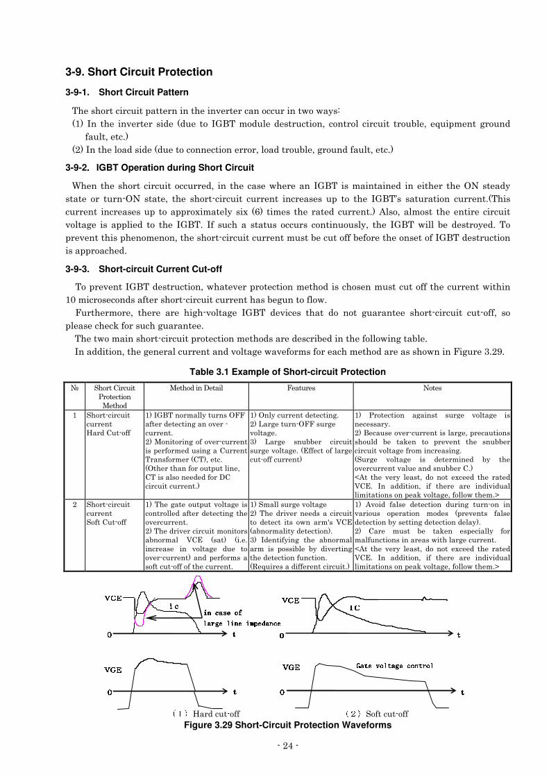
���(���
3-9. Short Circuit Protection
3-9-1. Short Circuit Pattern
�� ������������������� �������� ���� �� ���������������� �� �*�%�
����)�� �� ���� �� ����� � ��� � ���)/�������� �� ���������0� �������� �������� ������ 0� <���� ���!������
�����0� ��"��
����)���� ��������� ���� �������� ������ ����0������������ 0�!�����������0� ��"�� �
3-9-2 �� �� IGBT Operation during Short Circuit
, � ���� ��������������������� �0������ � ��� � � � ����)/�������������� ����� ��� �� �� �:���� ��*�
���� � ��� �����:�� ���� 0� �� � �������������� ���� ������� �� ����� ��� �� �)/��G�� ����������� ���� ��"������
���� ������� �� �������������$���� �*���$��'�� ��� �� �� ���� �� ���� ��"��2���0�������� �� � ���� � �������������! ���� ����� �� ��� �� �)/��"�)�� ����� �� ������� ������� �����������*0� �� �)/��� ����� � � ����* �"� ���
�� � ���������� ��� ���0��� ������������������� ��������� ���������� ��� ��� ���� �����)/���� ����������
����������� �"�
3-9-3. Short-circuit Current Cut-off
����� � ���)/���� ���������0� ��� � ������ ������� ������������ ����������������� ����� ��� ������
�������� ��������� �������������������� �������� !��������� "�
� � -���� ���� 0� �� � � �� � ��!�������! � )/��� � ��� �� ����� ��� ���� !������ � �������������� �������0� ����� �� ��� �1����������!������ "�
� � �� �� ������������������������� ������� �������� �� ����� ������� ������ ��!����� "�� � )����������0��� �! � �������� ������������! � �� ���������� ����� ������� ������� �����-�!�� �"�&"�
Table 3.1 Example of Short-circuit Protection
j� ;�����3�������+��� ������� �����
� ��������4 ����� - ���� �� ��� ��
�� ;����������������� ���.����3�������
���)/����������*�������:--���� ��� � ����!������ �������� ��"����� ��������!������ ������ ������� ����� ������!���3��� ������������ ���3��0� ��"��:�� ��������������������� 0�3����������� � ������43������������� ��"��
���:��*����� ���� � ����!"����#��! ������:--����! ������! "��� #��! � ����� �� �����������! ������! "����� ���������! ������������� ����
��� +��� ������ �!������ ���! � �����! � ���� � ����*"����� ���� ��� ������ ���������! 0��� ���������������� � � ��1 �� ��� �� � ��� �� � ����� ���������������! ����� ����� ����!"��;��! � �����! � ��� � � ���� �� �*� �� ��� ����� ������� ���������� ��3"��E2�� �� � � �*�� ���0� ��� ���� $� �� �� � ��� ��63�"� )�� ��������0� ��� �� � � �� � ��������������������������� �1������! 0������ ��� � "F�
�� ;����������������� ���;����3�������
����� �!�� �������������! ������������ ����� ��� � ����!��� ��� ����� ��"������ ����� ���������������������������� 63�� ������ ��" "����� �� � ��� �����! � �� � ����� ������ ��������� ��������������������������� ����� ��"�
���;��������! ������! � ������ ����� ��� ��� �� ����������� � � ��� ���� � �� ���>�� 63�������������*�� � ������"��� )� ����*��!� �� � ������������ � ��� ������� � �*� ��� ����!��� �� � ��������������"��5 <��� �������� � ����������"��
��� 2����� ���� � � � ������ �����!� �������� ����������� �� ������� ��� �� ��� � ���� ���� �� � �������*�� ����!�� � ������� ��*�"���� 3�� � ����� � � ��1 �� �� �����*� ���������������������� ��� �������! ����� ��"�E2�� �� � � �*�� ���0� ��� ���� $� �� �� � ��� ��63�"� )�� ��������0� ��� �� � � �� � ��������������������������� �1������! 0������ ��� � "F�
�
� � � �
�
�
�
�
�
�
�� �~���
.��������������1�
;������������Figure 3.29 Short-Circuit Protection Waveforms
��~��~��~��~���������������������
�� ��
�s�s��s�s��s�s��s�s��� ��
��������������������������������
�� ��
�s�s��s�s��s�s��s�s� �� ��
¡¡ ¡¡£¢¢ ¢¢v¤¦¥[§¦¨,©9ª¤¦¥[§¦¨,©9ª¤¦¥[§¦¨,©9ª¤¦¥[§¦¨,©9ª
«« «« ¥9¬�¨¥9¬�¨¥9¬�¨¥9¬�¨B9©b®¯¬¦¥9°�¨B¤¦©¦¢[¬¯±9©b®9©b®¯¬¦¥9°�¨B¤¦©¦¢[¬¯±9©b®9©b®¯¬¦¥9°�¨B¤¦©¦¢[¬¯±9©b®9©b®¯¬¦¥9°�¨B¤¦©¦¢[¬¯±9©b®
®® ®®¦¥¦±[°�¨¥¦±[°�¨¥¦±[°�¨¥¦±[°�¨v®9¡²¢[¨l¡²³9´[¨�µ¦¥¦¢[¤�¨®9¡²¢[¨l¡²³9´[¨�µ¦¥¦¢[¤�¨®9¡²¢[¨l¡²³9´[¨�µ¦¥¦¢[¤�¨®9¡²¢[¨l¡²³9´[¨�µ¦¥¦¢[¤�¨
�
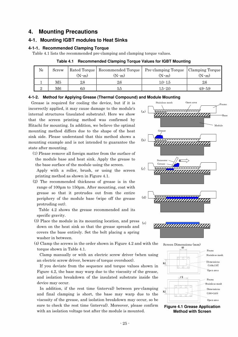
���8���
4. Mounting Precautions 4-1����Mounting IGBT modules to Heat Sinks
4-1-1 ¶¶ ¶¶ Recommended Clamping Torque � � ���� �("���������� �� ���� �� ���� ��������!������������!����<� ����� �"�
Table 4.1 Recommended Clamping Torque Values for IGBT Mounting
j� ;�� � 5�� �����<� �
�� · ���5 ���� �� �����<� �
�� · ���+� ��������!����<� �
�� · ���3������!����<� �
�� · ����� � 8� �"I� �"'� �"����"8� �"'�
�� � '� '"� 8"8� �"8����"� ("&���8"&�
4-1-2. Method for Applying Grease (Thermal Compound) and Module Mounting /� �� � ��� � <��� �� ���� ������!� �� � � ��� 0� ���� ��� ��� ���
������ ���*������ �0������*����� �����! ������ ������ >��
��� ����� �������� �� �������� �� �������� �"� . � � � ��� �
����� �� � ��� �� �������!� � ����� ��� ������� �� �*�
.������������������!"�)����������0� �� �� � ��� ���������
�������!� � ����� ���� ��� �� � ��� �� � ���� � ��� �� � � ���
���1� ��� "� +� �� � ��� ������� ����� ����� � ����� ��� �� ��
�������!� $���� ��������������� �� �� ���!������ � �� �
���� ���� ���������!"�����+� �� �� ��� �������� �!������ ������ ��� ������� ����
�� ������ ���� � ����� ��� ���1"�2���*� �� �!� �� � ���
�� ���� ������� ������ ������ �����!��� ���� �"�� � 2���*� ���� �� ���� �0� �����0� ��� ����!� �� � ��� ��
�������!�� ����������� �����-�!�� �("�"����� �� � � ���� �� �� ����1� ��� ��� !� �� � ��� ��� �� �
���! �����R������8R�"�2�� ���������!0������ ����
!� �� � ��� ����� ��� ������� �� ���� ���� � �� � ���� �
� ���� �*� ��� �� � ����� � ��� � � �� � ���� �� � !� �� �
���������!�����"�
� � � ���� � ("�� ��� �� �� � !� �� � � ���� �� �� ���� ����
�� ������!�����*"�
���+��� ��� ������ ���������������!���������0������� ���
�� ������� �� ������1����������� �!� �� ���� ��������
��� ��� �� ���� � ���� �*"�; �� �� ������������!��� �����!�
��� ������ � �"��(��3������� ���� ������� ���� ����� �����-�!�� �("������ ������ �
���<� ���� ��������� �("�"�3������������*� ��� ���� ��� � ������ ��� � ���� �� � � ������!�
��� � ��������� ����� �0�� �� �������<� ��� �������"�
)�� *��� � ���� � ���� � �� � � <� �� � ���� ���<� ����� �� ��� �����
-�!�� �("�0��� ���� ���*� ������ ������ ���������*������ �!� �� 0�
���� ���������� �� �1�� �� ��� �� � ������� �� �������� � ����� � �� �
� ��� ���*������"�
)�� ��������0� ��� �� � � ��� ��� � ���� ������ � � �� �� ��������!�
���� ������ �������!� ��� �����0� �� � ��� � ��*� ���� �� � ��� �� �
��������*������ �!� �� 0����������������� �1�� ����*������0����� �
��� � ��� �� �1� �� �� ��� ��� � ���� �����"�� �� �� �0��� �� � ��������
����������������������! �� ������ ���� ������ ��������� �"��
Figure 4.1 Grease Application Method with Screen
¸� ¹
¸� ¹
¸� ¹ �
¸� ¹
¸ ¹
;����� ���� ��� :� ���� �-���
���
� ����
/� ��
/� ��
;<� !
º » �
º²¼ �-���
;����� ���� ��
4�� ������½�($�¾:� ���� �¿ À ¼
º²¼ �-���
;����� ���� ��
4�� ������
��&O�( ¾:� ���� �
;�� ��4�� ������������
�
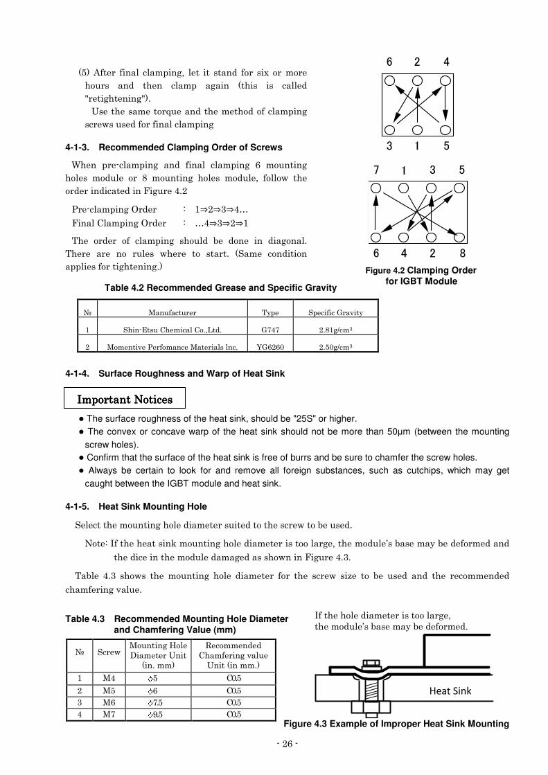
���'���
�8��2�� �� ������ �������!0�� ����� ������ ���� ��$������� �
������ ���� �� �� ������ �!���� ������ ��� ���� ��
C� ��!�� ���!C�"�A� ��� ���� ����<� ������� �� ���������������!�
��� ���� �������������������!�
4-1-3. Recommended Clamping Order of Screws
, � �� �� ��������!� ���� ������ �������!� '� �������!�
��� �� ����� � ��� I� �������!� ��� �� ����� 0� ����� � �� �
��� ��������� �����-�!�� �("��
+� ��������!�:�� �� %� � �����(U�
-�����3������!�:�� �� %� � U(������
�� � ��� �� ��� �������!� ������� � � ��� � ��� ���!����"�
�� � � �� � ��� ��� �� � � � ��� �����"� �;�� � ����������
����� ��������!�� ���!"�� �
Table 4.2 Recommended Grease and Specific Gravity
�
� � � � � � � � �
� �
4-1-4. Surface Roughness and Warp of Heat Sink
� �
� � � � � � � � � � � �
� The surface roughness of the heat sink, should be "25S" or higher. � The convex or concave warp of the heat sink should not be more than 50�m (between the mounting
screw holes). � Confirm that the surface of the heat sink is free of burrs and be sure to chamfer the screw holes. � Always be certain to look for and remove all foreign substances, such as cutchips, which may get
caught between the IGBT module and heat sink.� � � � � �
4-1-5. Heat Sink Mounting Hole
; � ����� ��������!���� ����� � ������ ������� ���� ����� ��� �"�
��� %�)���� �� ������1��������!���� ����� � ������������! 0��� ������ G����� ���*�� �� ���� ������
� � � �� ���� ������ ������ �����! �������� �����-�!�� �(""�
���� � ("� ��� �� �� ��������!���� � ���� � �� ���� �� � ��� � ��? � ��� � � �� �� ���� �� � � ���� �� ��
����� ���!����� "�
�
Table 4.3 Recommended Mounting Hole Diameter and Chamfering Value (mm)� � � � � � �� �
� � � �
�
�
�
�
� � � � � � � � � Figure 4.3 Example of Improper Heat Sink Mounting
)�������������� �)�������������� �)�������������� �)�������������� �����
j� ;�� ��������!�.�� �4��� � ��A�������"�����
5 ���� �� ��3���� ���!����� �A����������"��
�� �(� �������� Á 8� 3"8�
�� �8� �������� Á '� 3"8�
� �'� �������� Á 7"8� 3"8�
(� �7� �������� Á &"8� 3"8�
�
j� ���������� �� �*� � ;� ������/�����*�
�� ;���������3� ������3�"0#��"� /7(7� �"I�!L���
�� ��� ���� �+ ������� ���� ���������"� J/'�'� �"8!L���
�
� ��
� ��
� � ��
� � ��
��������
�
Figure 4.2 Clamping Order for IGBT Module
)���� ���� ����� � ������������! 0��� ������ G����� ���*�� �� ���� �"�
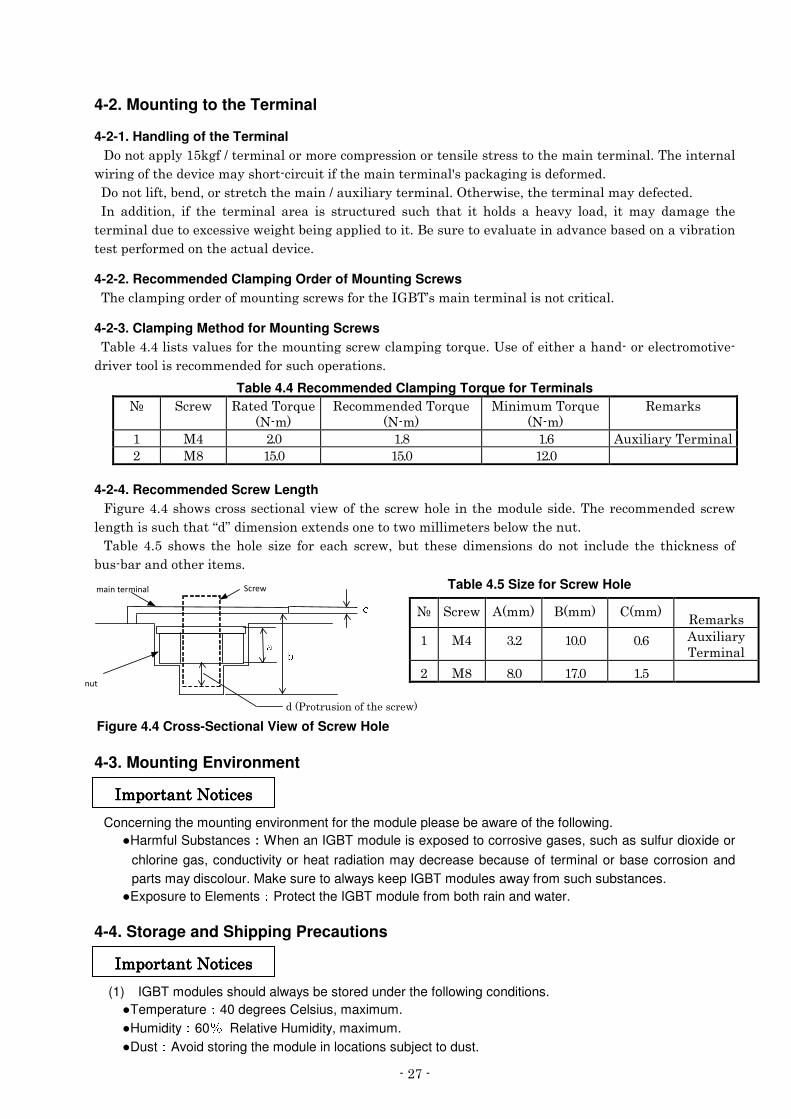
���7���
4-2. Mounting to the Terminal
4-2-1. Handling of the Terminal 4����������*��81!��L�� ������������� ������ ���������� ���� ���� �������� ������� ������"��� ���� �����
����!������ �� ��� ���*�������������������� ������� ������>�����1�!��!����� ���� �" �
4����������0�� ��0������� ������ ������L���$�����*�� ������"�:�� � �� 0��� �� ���������*�� � �� �"�
)�� ��������0� ��� �� � � ������� �� �� ��� �������� �� ����� ����� ��� ������ �� � ��*� ����0� ��� ��*� ����! � �� �
� ��������� ���� $� ���� � �!���� ��!������ �������"�� ���� ���� ������ ���������� ���� �����������������
� ���� ����� ������� ��������� ��� "�
4-2-2. Recommended Clamping Order of Mounting Screws �� ��������!���� ������������!���� �������� �)/��G�������� ����������������������"�
4-2-3. Clamping Method for Mounting Screws ���� �("(����������� �������� ��������!���� ��������!����<� "�A� ���� ��� ������������� � ��������� ��
���� ����������� ���� �� ������������� �������"�
Table 4.4 Recommended Clamping Torque for Terminals j� ;�� � 5�� �����<� �
������5 ���� �� �����<� �
�����������������<� �
������5 ���1��
�� �(� �"� �"I� �"'� 2�$�����*�� ��������� �I� �8"� �8"� ��"� �
�4-2-4. Recommended Screw Length -�!�� �("(���� ��������� ���������� ������ ���� ���� ������ ������ ���� "��� �� ���� �� ����� �
� �!����������������X�Y���� ������ $� ������ ����� �������� � ���� �� ��� ����"�
���� � ("8� ��� �� �� ���� � ��? ����� ���� ��� 0����� �� � � ��� ������� ������� ������ � �� � ����1� ��� ���
��������������� ���� ��"�
� � � � � � � � Table 4.5 Size for Screw Hole �
� � � � � � � � � � �
� � � �
�
�
�
��4-3. Mounting Environment �
�
Concerning the mounting environment for the module please be aware of the following. �Harmful Substances  When an IGBT module is exposed to corrosive gases, such as sulfur dioxide or
chlorine gas, conductivity or heat radiation may decrease because of terminal or base corrosion and parts may discolour. Make sure to always keep IGBT modules away from such substances. �Exposure to Elements à Protect the IGBT module from both rain and water.
4-4. Storage and Shipping Precautions �
�
(1) IGBT modules should always be stored under the following conditions. �Temperature  40 degrees Celsius, maximum. �Humidity  60 Ä Relative Humidity, maximum. �Dust  Avoid storing the module in locations subject to dust.
j� ;�� � 2����� ������ 3�����5 ���1��
�� �(� "�� �"� "'� 2�$�����*�� �������
�� �I� I"� �7"� �"8� �
�
)�������������� �)�������������� �)�������������� �)�������������� �����
)�������������� �)�������������� �)�������������� �)�������������� �����
���+��������������� ���� ��
Å ÆÇ
��
������������ �����
�
Figure 4.4 Cross-Sectional View of Screw Hole
���I���
�Harmful substances  The installation location should be free of corrosive gases such as sulfur dioxide and chlorine gas. �Other  Do not remove the conductive sponges or tapes attached to the signal gate and emitter gate.
����;������!�� �����
�To prevent the case cracking and/or the electrode bending, appropriate consideration should be given to properly insulate the shipping container from mechanical shock or sever vibration situation. �Do not throw or drop the case while shipping. Treat them with care. The devices may break if they are
not handled with care. Please do not use the IGBT modules that were dropped or damaged. �Appropriate labeling on the outside of the shipping container should always be present. �The shipping container itself should always be properly protected from both rain and water.
4-5. Precautions against Electrostatic Failure
�
�
Because the IGBT has a MOS gate structure, you should always take the following precautions as measures to avoid generating static electricity. �Before starting operation, do not remove the conductive sponge or tape mounted between gate and
emitter. �When handling the IGBT module, ground our body via a high-value resistor (between 100k� and 1M�),
hold the package body, and do not touch the gate terminal. �Be sure to ground any parts which the IGBT module may touch, such as the work table or soldering
iron. �Before testing or inspection, be sure to check that any residual electric charge in measuring
instruments has been removed. Apply voltage to each terminal starting at 0V and return to 0V when finishing.
4-6. IGBT Module Circuit Arrangement and Wiring Method ���� � +��� ��� �)/�������� ������� ���������? ��� � ����!� ��������� �������� ��� �������*"� )������� ����!� ��������� � � ��� �� ���! 0� ��� ��*� ! � ��� � ��� �� ������� �����! � �����!� � ������!� ����� ����*� �� � )/�������� "� )�� ��� �� ��� � ��� � ��������� � ��� �� ������ �������� ����!0� �� �� � �� �������� ����������"�
���� � 2���1 ���� ����� �� � ���� �!�� �������������)/�������� �������������������� "�)���� ����� �������!0� !�� � �����! � ���� ��� � ��� ����� ��� � ��� �*� ���� �� � � ������!� ��� � ���� � ��� � ���! �"� )����������0��� ���1 �������������� �! � ������� ����� ����� �� �"�)����� ������ ��� � ����!���������� ������� � ������� 0� ��� ����� �� �� ������� ������ ������� �� ������ ��������� ��� �"�
4-7. Measurement Precautions ����� ��� �� !�����!�63�;�� ���� � ���0�� ���� �������������������� ���!����!�� ����� ���� ��� �������"�
)�� �� � ��!���� !�� � ���� ���� �� � �������� �� � 1 ��� �� �� ��� �� ��� �������� ��� � � ���� � �����!�� ���� � ��0��� �)/�������� ���*�� �����! �"�)����������0������ � ���������1�������� ������������� ������ ��� ������� ����*�� �� ��������� ���������0���� �� ��*��!� ���� ��� � ����� �� ������ ��� �����$"� ��0� � ���� � ������ �� � �� ���� �� � �� ����� �����������"�
����, �������� �)/�������� 0������� ���������� � ���� ����������� ������ ������� � $� ��������� ������� ������"��� ������! ������ ������� ������������ ������! ������ � $� ������ ������� ������� �� ������0� �� �����*������!�� ������!"�-��� $�� ����!� �� � ��� � ��� � ��� ����! � ��� ���� ��� ��� ��L��� ���� �� � ���� � ��������� � ��� #0� ����������� ������! � <�������#O��L��� ����� �! � ��� �� �������� ����� "��*������*0����� ���������� �#���� ������ �� ��� (� �."� ;�� � �� �� � )/��� ����� � ��� ���� �� :�0� �� � $� ����� � ������� �����! ���� �� �������!� ��������� ������! ������ ���������"�3��� �� �*0� � ���� �)/�������� �������� ��:--0��� ���� �� �� $� ������ ������������! ������ ��������� ������! ������ ������� �����"��� ������! ������ ������� ������������������ �� ����� ����� $� ���� ���� �������! ������ �� ��� "�
)��)��)��)�������������� ������������� ������������� ������������� �����
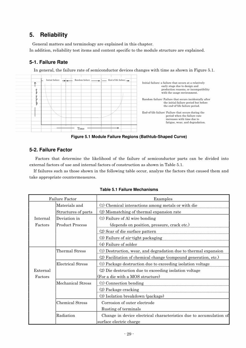
���&���
5. Reliability / � �������� �������� �������!*��� � $����� ��������������� �"�
)����������0�� ��������*�� ����� ����������� ����� ����������� ������ ��������� ��� � $����� �"�
�
5-1. Failure Rate )��! � ���0��� ������� ���� ����� ������������� ��� ������! �� ������� ������� �����-�!�� �8"�"�
�
Figure 5.1 Module Failure Regions (Bathtub-Shaped Curve) �
5-2. Failure Factor
-������� ����� � � ���� � �� � ��1 ������� ��� �� � ������ � ��� � ������������ ������ ���� � � ����� �� �����
$� ������������������ �������� ����������������������������������� ��������� �8"�"�
)�������� �������������� ���� ������� ������ ��!����� ������0�����*? ��� ������������������ ���� ������
��1 ����������� ������ �� ���� �"�
�
Table 5.1 Failure Mechanisms
-����� �-������ �$���� ��
� ��� ���������� � ����3� ��������� �������������!�� �������� ������ �
� ;������� ����������� � ��������������!������ ����� $����������� �
)�� ����� 4 ����������� � ����-����� ����2�� �� �������!�
-������� +�������+��� ��� �� � ���������������0��� ���� 0�����1� ��"��
� � � ����;��������� ������� ����� ���
� � � ���-����� ����������!������1�!��!�
� � � �(��-����� �������� ��
� �� �����;�� ��� � ����4 ���������0� ��0������ !����������� ������ ����� $��������
� � � ����-����������������� ����������! �����������! � ������0� ��"��
� �� ��������;�� ��� � ����+��1�! �� ������������ ���� $� ���!����������������! �
�$� �����
-�������
� � ����4� �� ������������ ���� $� ���!����������������! �
�-������� � �������:;��������� ��
� � ���������;�� ��� � ����3��� ������� ����!�
� � � ����+��1�! �����1��!�
� � � ���)����������� �1�� ������1�! ��
� 3� ������;�� ��� 3��������������� �� � ����� �
5�����!����� ��������
� 5��������� 3���! ����� ��� � � ��������������� ���������� ��������������������
������ � � ����������! �
È#É#Ê*Ë!Ì�Í�Î*ÏÑÐ*Ò1ÓnÔ$Õ�Ö�×�ØÑÉqÙ�Ú�Û�ÜÑÝ�Þß Ü#à�á#â�Í#Î�ãnävåsÒÑæ�ç�èéÙ$ê1ë1ìíïî�ð Ê�Ë1ñònó Ê*Ë!Ì9È#É#Ê*ËnØ1Ééôsõ,öÑÜ1÷nø�Ê*Ë#ØÑÉéÙÑùð;únû Ò�Ø1ÉqÙ ònó Õ�Ù ó�í#ü,ð Ê$Ë�ñ÷nø�Ê*Ë!Ì�ý*þnÜ�÷�øqÜ�ÿ���������sÙ*ê1ë�ìnÜ#Ø�å#å���Ù;Ê*Ë� �������� ð Ø1ÉqÒÑÊ$Ë�ñ
������� ������� �!����
"�#
÷ ø�Ê Ë)������������� %��������� ������������������� ����� �*��
���*����! ��� ����� ��!����������������� �����0������������������* ������ ����! � ������� ��"
5������������ %�-����� ������������������ �����*���� ��� ��������������� �� ���������� ��� ��� � ��������� ������� �� ����"
���������� ������� %�-����� ������������������!��� � ����� � ���� ������� ���� ���� �� �� ������� ��� ��������!� 0� ��0������ !��������"
5������������ )������������� ���������� �������
���
-����� ����
�����
5-3. Reliability Test
5-3-1. Reliability Test Types and Descriptions
�$���� ������� ��*� ���������� �������� �� ��������*�� ����� ����� ���*�.������������ ������ ���������
�� ���� ��������� �8"�"�
Table 5.2 Reliability Test Types and Descriptions
j� �*� ����� ��� � ���� ���������4 �����������
�� � �� ����� �
3*����!�
4 � ���� ��� ���� ���� � � �� $��� ������������!�������� �� �� ����� �����������"�� �� ����� %���� �� �� ����� 0�������� � �� ����� 0� ������!�� � �� ����� �0� ��� %� '������ �� ���0����� ������*�� �%���
�� � � � � ���������
� � � � � ����1�
4 � ���� ��� ���� ���� ��������1"�2�� � ������%��/0�4�� �����%��k0�J0�l�0���� %�'R�"�+ ����� ����� ���� ����� ������� �����"�
� � ���������
6���������
4 � ���� ��� ���� ���� �������������"�2�� � ������%��/0�-� <� ��*%��.?��1.?0�4�� �����%��k0�J0�l�0������������ ������� ������
(� ;�� ����<� �
������� �������L�
�������!��
4 � ���� ��� ���� ���� ������� ����<� � � ���������!��� ������� ������0� ��"�;�� ����<� %��� ���� �����<� 0�;����! ���� %�'�������
�
8�
� � )�� �������!� �
�� ���������� �
4 � ���� � �� � � �������� ���� � ��������� ��� ���� � ��� �� � � ��� � ���� � �� ��� ���� �� ����� ���� ������������ ������� ����� ���������������������� ��"�T���9�7�30�8�.?��������� � �� 0�)��9���� ������ ����)/����Im�-, 4�&m��� �0����� ������*�� �%�0�
'� 2���� ��43�
6����! �
4 � ���� ��� � � �������������� �������� ���� ��*�����*��!� � �������������� �������� ����� �������!�� ����������� "���%���8��30�2���� �������! %�IM������ ���� �������! 0�2�������������� %��0�������
7� 2���� ��23�
6����! �
4 � ���� ��� � � �������������� �������� ���� ��*�����*��!� � �������������� �������� ����� �������!�� ����������� "���%���8��30�2���� �������! ��� �1����� �%���� ������ 0�2�������������� %��0�������
I� .�!��� �� ����� �
;����! �
4 � ���� ��� ���� ���� � � ������ �������!��� �� ����� �"���%���8��3����� ����$����������! �� �� ����� �0�2���� ����� %��0�������
&� #� �� �� ����� �
�����! �
4 � ���� ��� ���� ���� � � ������ ������� �� �� ����� �"���%��(��3����� ���������������! �� �� ����� �0�2���� ����� %��0�������
�� .�!���������*� 4 � ���� � �� � ��� ���� � ��� �� � ���� �����! � �� �� �� ���!� � ����� ��� ��� � ��� ��!��� �� ����� �������!���������*"�5.�9�&M0���%�'��30�;����! ���� %��0�������
5-3-2. Reliability Test Reference Values
� � �� � ���� ���� ���� � ��� � � !��������� ���� �� � ���� � � ��������*� � ���� �� � � � ���� �� �*� �� � ����� ��!�
�� ����������� �"�
����)� �0�)! ��E �"���� ����� ������ "�
����6� �����0�6��E �"����� ����� ������ "�
���5���=����E �"8���� ����� ������ "�
5-3-3. Sample Testing Criteria
�� ����� ���������� �����������L���������� ���������� �� ��������*�� ����� ��������� ���������� �����;���� �  '��� � ������ ����� ����������� �����5 = ����  �5 = �������� �� �
5-3-4. Reliability Test Period
�� �� ������ � ���� �� ��������*�� ������ �������� ���� ��������� �"�
����5 ��������*�� ������ �������� �� � ���� ���������������*� ��������� � ���� � ���� ������! �"�
����5 ��������*�� ������ �������� �� � ���� �������������*� ��������� � ����������������������! �"�
��� � ��� ���� �� � ���� �� ����!�������������� �� ������������� ��!����� ���������� �������� ������ �"��
������
5-3-5. Test results (example)
�� ����� �� �� ���� ���� �� ��������*�� ����� ���������������������������������������"�
����)/�������� ��� ��� �
� �*� ���"�%���������
� 5����!� %�06L�0�2�
� �=� %��( $ ��8������� ����� ������������������
� � �������%�� ����*� ����������������
�Table 5.3 Reliability Test Types and Testing Conditions
� �*� ����� ��� � ���3���������;���� �
;�? �
��"����
+��� ��
�������� �����-�������� .�!��� �� ����� �;����! �
� �� ����� % ��8���;����! ���� % �0�� '� '�
#� �� �� ����� �;����! �� �� ����� % �(��� �;����! ���� % �0�� '� '�
� �� ����� ��*����!�
�(����5�������8��.������� %�'������ �� ����� �� ����� ����� ������ � ��������*�� �� % ��
'� '�
.�!���������*�� �� ����� % '��.������* % &M5"."���� % �0�� '� '�
� ��"�.������*�
;����! �
� �� ����� % I8��.������* % I8M5"."�6����! % �"'16430���� % �0�� '� '�
� ���������-��������
6������������
6������ �-� <"�
2�� � ������D��/0�-� <� ��*�5��! D��.?& �1.?�4�� ������%������������ ����k0�J0�l�
'� '�
6������������
6������ �-� <"�
�������������� ��"8��0�-� <� ��*�5��! D��.?& 88.?�4�� ������%����������� ����k0�J0�l�
'� '�
6�����������
6������ �-� <"�
2�� � ������D��/0�-� <� ��*�5��! D�'\�.?0�� ������ 0�4�� �����D������������ ����k0�J0�l�
'� '�
� �������������1�2�� � ������D��/0�+��� � ����D�'���� ������ 0�4�� ������%���*�� ����� ����k0�J0�l�
'� '�
�������!���� �!����� ���� �����<� � � �����! �%�'�0�� �� ����� �%�5�0��R�� � 2������
'� '�
�� �������� �!����� ���� �����<� � � �����! �%�'�0� �� �� ����� %5�0�-2������R�n�� � 8� � 3������ �
'� '�
�� ��������-��������
� ��" �����23��� ��"D���8� !"30�!�� � ���� ��������2���*�6����! D�06��3����� �����������D��0��
'� '�
� ��" �����43��� ��"D���8� !"30�!�� � ���� ��������2���*�6����! D��0'6��3����� �����������D��0��
'� '�
� ��" �����23��� ��"D���8� !"30����� ����� ���� ��������2���*�6����! D��6��/����� �����������D��0��
'� '�
�� �����-���!� �� ���)-9�0�2� � ��97�� � 6/�9�86� � 0�3*�� ����� �)/�� % �Im0� � 4��� %&m� '� '�
+� ��3*�� �)39�0�2�)/������ ���=9'� ' � �0��*�� � '� '�
�� �����������
4������! �
3���������3D���-0�5 ������� 5D�`�� ���6����! D��60����� ����� ���� ��������
'� '�
)���������2���� ��6����! D�8076���OI���"�N�(086���O�����"�K��!� ��%����� ������������� ��� ����n��2��
'� '�
��������
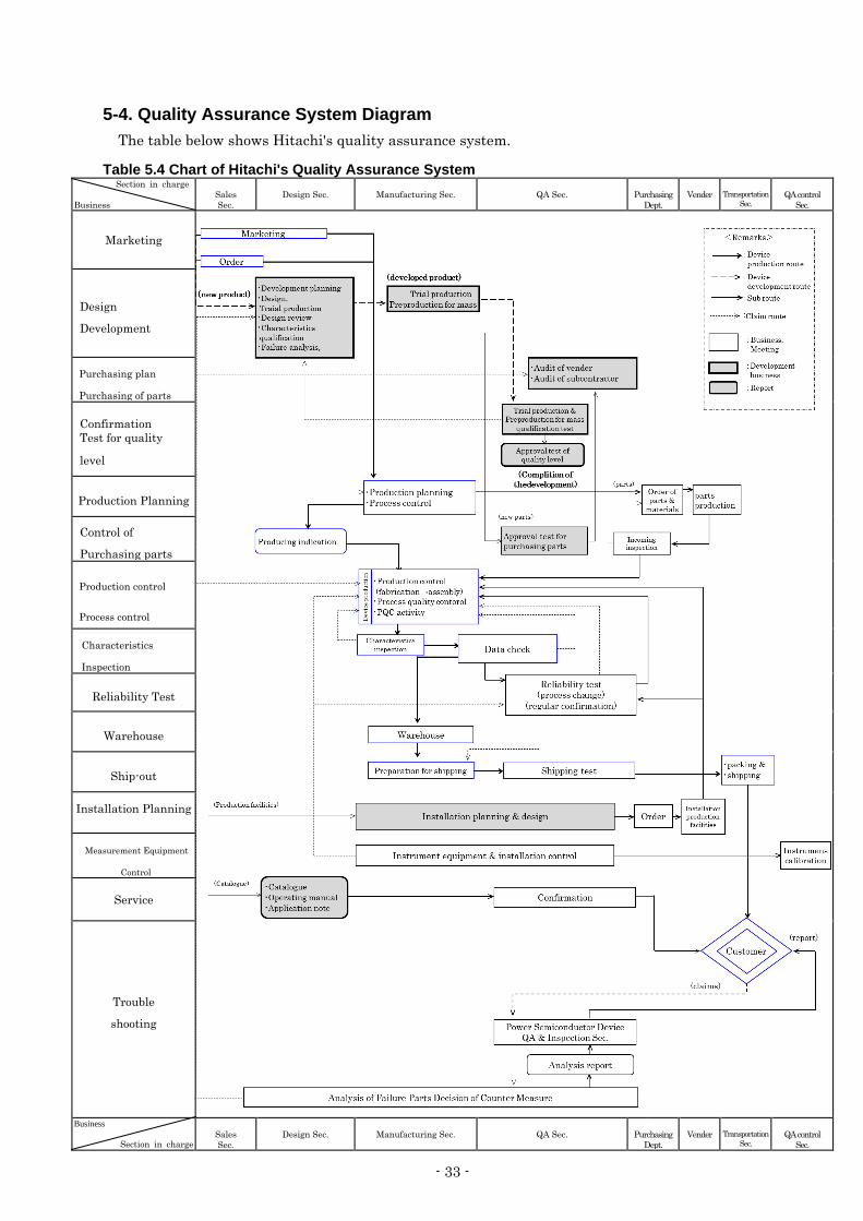
- 33 -
5-4. Quality Assurance System Diagram
The table below shows Hitachi's quality assurance system.
Table 5.4 Chart of Hitachi's Quality Assurance System Section in charge
Business
Sales
Sec.
Design Sec.
Manufacturing Sec.
QA Sec.
Purchasing
Dept.
Vender
Transportation
Sec.
QA control
Sec.
Marketing
Design
Development
Purchasing plan
Purchasing of parts
Confirmation
Test for quality
level
Production Planning
Control of
Purchasing parts
Production control
Process control
Characteristics
Inspection
Reliability Test
Warehouse
Ship-out
Installation Planning
Measurement Equipment
Control
Service
Trouble
shooting
Business
Section in charge
Sales
Sec.
Design Sec.
Manufacturing Sec.
QA Sec.
Purchasing
Dept.
Vender
Transportation
Sec.
QA control
Sec.
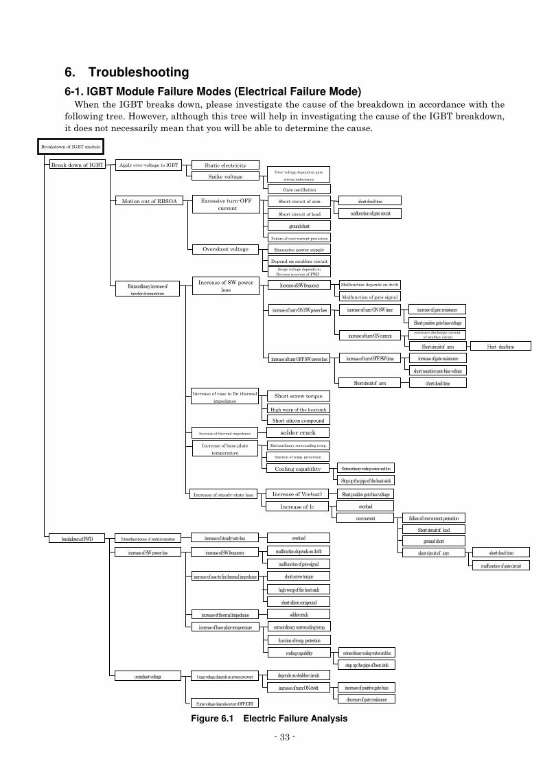
�����
6. Troubleshooting 6-1. IGBT Module Failure Modes (Electrical Failure Mode) , � ���� �)/����� �1���� �0��� �� ���� ���!�� ��� ����� ������ ��� �1�� �������������� � ������ �
����� ��!��� "�.� � �0�������!��������� � ����� ��������� ���!����!��� ����� ������ �)/����� �1�� �0������ ������� � ������*�� ��������*��� ����� ���� ����� � ���� ��� ����� "�
� � �Figure 6.1 Electric Failure Analysis
���� �� ����!�� �� ������� �
���� �� ����!�� �� ������� �
�� ������ ���
�� ������
�� �1�� �����)/�������� �
�� �1��� �����)/��� 2���*��� �������! ����)/��� ;������ � �������*�
;��1 ������! �:� �������! �� � ������!�� �
����!���������� �
/�� �������������
��������������5�;:2� �$� ���� ������:--�
� ���� ���
:� ������������! �
;�������������������
;���������������������
!������������
-����� ������ ������ ������� ������
������� ������ �
���������������!�� ���������
�$� ���� ��� �������*�
4 � ����������� ����������
�
)��� �� ����;, ��� ��
�����)��� �� ����;,��� <� ��*�
���������������!�� ���!����
���� �� ���������:��;,��� ������� ���� �� ���������:��;,���� �
;������������ �!�� �����������! �
���� �� ���������:������ ���
;���������������������
���� �� ���������:--�;,��� ������� ���� �� ���������:--�;,���� �
������� !���� �!�� �����������! �
;��������������������� ������� ������ �
)��� �� ������� ���������� �����
��� ���� �;�������� ����<� �
.�!�� ��������� �� �����1�
Short silicon compound
)��� �� ������ �������� ���� � ���� ������1�
)��� �� ������� ����� �
� �� ����� �
3�����!����������*� �$����������*�������!� �� ����������
;��������� ���� ������ �� ������1�
)��� �� ������ ��*����� ������ )��� �� ����6� �����
)��� �� ����)��
������ ������ ������ ������� ������
;����������������������
!������������
���������������������� ������� ������ �
���������������!�� ���������
�� �1�� �����-,4� �$����������*����� �� ������=��������� �� ����� � ���� �� ������ ��*���� ������ �� ������
���� �� ����;,��� ������� ���� �� ����;,��� <� ��*� ������������� � ���������L���
���������������!�� ���!����
���� �� ������� ���������� �������� ���� � ��������� ����<� �
��!�� ��������� �� ������1�
�����������������������
���� �� ������ �������� ���� � ���� ������1�
���� �� ������� ����� �� �� ����� � $����������*�����������!�� ��"�
������������� ��"����� ������
������!����������*� $����������*�������!� �� ����������
�� ������������! � ;��! ������! �� � �������� � �� �� ��� �*� � � ������������ ����������
���� �� ���������:����L��� ���� �� ����������� �!�� ������
� �� �� ����!�� �� ������� �;��! ������! �� � ������������:--�)/���
;������� ������ �
���������� ���� ����� ������1�
;��! ������! �� � �������
5 � �� �� ��� �*����-, 4�
�$����������*�����������!�� ��"�
������������� ��"����� ������
������������� � ���������L���
;������������ �!�� �����������! �
$� ���� ��������! ����� ����������� ����������
�$����������*����� �� ����
=��������� �� ����� �
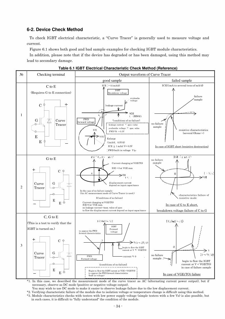
��(���
6-2. Device Check Method
����� �1� )/��� � ��������������� ������0� ��X3��� ����� �Y� ���! � ����*� �� �� ���� ���� ������! � ����
���� ��"�
-�!�� �'"����� �������!����������������� � $���� �������� �1��!�)/�������� �������� �������"�
)����������0��� �� ���� ����������� �� ��� ������ !��� ���������� ������! �0�����!������� �������*�
� ������� ������*�����! "�
Table 6.1 IGBT Electrical Characteristic Check Method (Reference)
� Checking terminal Output waveform of Curve Tracer
good sample failed sample
1
C to E
�5 <��� ��/���������� �������
(( ((
)) ))
/
3
�
�
3��� ���� �
VCE� * 200V/d �
� �1�! ����� ��
�������� �����!
-, 4��� ���������!
)/���� �1�� �������!
63�
)3�
+
)3�� , ���2o 69�"6--, 4���������������! 6� .
���2L�/ "86L��
� �1�! ����� ���� 0 �� �"�����
1����������������������� 2
)3�- * "��2L��
+
�������� ������! �� 3 �� �"�����
-, 4�6� 9�"6
�����!
4�5�6
798;:�< =?>;@BADCFE�>G@IHIJLK
M�N�O 6
PRQ�SUT�VWS�XZY [ \ ]_^W`�a
������ �����
��������� �����
� ������ �������� ��������� � ����:���
`�
)3����2����� � ����� �������2L���
)����� ����)/����������� ������ �� ����������
2
G to E
/
3
�
bb bb
cc cc �
3��� ���� �
dfe;gih jlknmpo9qsrutGowv;x y
zp{}|�~��l� �l��|�� � �9���Z���Z� �
�������W�������
�����¡ Z¢�£Z¤p¥�¦i§ |��Z����¨©���
ªLe;g« ruªfv;x¬y�
G®G¯ ° ±?²?³ |�~¡´�µ��i|��¡� ¦�¶¡· �B�
¸�¹iº ¢p»�¼ ° ½�¾�¿©À�Á�¾�Â�¾ZÃÅÄ?ÆlÇ�¾©ÈB³
ªLeGg «lÉ?Ê;ËWÌDÍ�Î�Ì©Ï�Ð�Ñ©Ò�Ó�Ô ÕÖZ×�Ì�Í twØGÙ ÎDÌDÏ�ÐBÚnÛiÜUÝ¡Þ�Ô�Õ;� � ß�à ÎW�©Ö�×�ÌDÍ�Î�á�âpã�äZÌ�Ï�åWÞ�æDÕçWè�é�ê �Wë�ì�íDÑ�î�Ì©ÏRÐ�ÏWï�Ô�Õ
ð3���������������������� ñ
3��� �������!��!����6/���:�)/�9����6/����$"���� �1�! ����� ���E��$"����� ������ ������� ��� �������� � ������� ���� � ����������������������
������� � ������� ���� � ����������������������
3��� �������!��!����6/���:�
)/��9�����6/����$
)���� ���� ������������� ������ �2��23�� ���� � ������ ����3��� ����� ������� �"�
ò
ó�ô_õ
ö÷�øùûúWüFý�þÿ��
���������� ������
������ ������ �
��������� ��� ��
������� �������������� ���� ������ �� ��
)����� ����/�����������0�
�� �1�� �������! ������� ����3����/
3
C, G to E
������������ ������� ���*�������� �
)/���������� ����"��
�
/
3
�
bb bb
cc cc �
3��� ���� �
��������� � !�"$#&% ' ��(�!)+*-,.*�/+02143 5
6�7989:<;>=@?BA�C D
EF7$8<?�G<E�A�C DH
6JI�K�LMON�PQ�R�S@TVU&WYX , Z
[�3 5
\�]�^@_ MO`ba
���c������� !$"�#&%c' ��(�! )+*-,.*�/20+1d3 5Q�R�S@TVU&WYXB��eFfhg�ikj )2l # ,YZb[�3 5
mon4p-q T r2s t
uYT v+w-%4x )+*,�y2z�{+|Y*�/B}
)/��-�� ��������!
� !��������� ��� )/������ ������6� ~ 6/���:�
���� ����
m�����������������������
t
� !��������� ��� �)/������� ������6/��9�6/���:������� ����� �-, 4���� ����������� ����������������������! �
������ ����� �-, 4��� ����������� �������
-, 4-�� ���������!
���J�<��������@���
��J����������� �
�
����������������h������� �o¡�¢ £¤h¥�¦�§�¨ª©«¨�¬®b¯
��������� �����
� !��������� ��� �)/������ ������6�E�6/���:������� ���������� ������
In case of VGE(TO) failure
p�"� )�� ����� ��� 0� � � ����� �� �� � � ���� � ��� ��� � ��� �� � ���� � ���� �� ��� 23� ���� ������!� ���� ��� �� �� �������0� ���� ���� � ����*0���� �� ����43���� ��������� ����� !���� ������! ��������"�J�����*� ��������� �43���� ������1 ���� ��� �������� �� �� �1�! ������� ��� ������ ��� �������� � ������� ��"�
p�"�6 ���*��!�������� ������������� ������ ������ ��� �������������������! ����� �� ����� �����! ������������������!������� ����"�p"�� ���� �������� ���������� �1�� ����� �� ��� ������ ��� �������*������! ������� �� �� ��� ������� �6������������������ 0���������������� �0��������������������C����*���� ������C��� ���������������� ������ "�

��8���
7. Failure Precautions 7-1. Warnings
7-1-1. Precautions for Package Bursting �
! ���� , 25�)�/, 25�)�/, 25�)�/, 25�)�/
�� , � �� ��� �� �� ������ ��� ��� �� ������ �������� ������� ��� ��� )/��� ����� 0� ��� ����� � � ���� �� :--�
��� ���� �*�� ��������� �� ����� ������"�
:�� � �� 0��� ������ ���� ���*������"
����� ���� ���� � � �!*���� �� � ��� ���� ������ ����������������� �� ��� �� ������ ����� ����� � � � �� ��
��������� ����*"�
2� �*��� �� �����������*�����1 ��� ������ ��!��� ��������%�
���b ���� �)/�������� ���������� ����� ������ � ����� ���������� ����������� � �������"�
��� � � �� �� �� �� � )/��� ����� >�� ���� �� ��� � ��� � ��� � ������ ���� ��� ��� � ��!� ������ �� ��� �� �
����� "�
7-1-2. Warnings against Burns and Electric Shock
! ���� , 25�)�/, 25�)�/, 25�)�/, 25�)�/
��4������!��� �������������� ��������� � ���������� � ����"�
;��������������*����� ���������� � ����������1"
7-2. Cautions
���� @@@@ ���� 33332A�):�2A�):�2A�):�2A�):�
��2�� ���� �)/����� �1���� �0� ���� �������������������������� ����� ������������� ���� ����������!���� �
�� � ��������� ��� ����� ������" �������*����� ����1 ������� "�
2�����!��)/�������� ���� ���� �� ����������� ����0���������A#&(6:0�*������������ �*����1 ��� ����
��� ���� ����������*�������� ����� ������ "�