Embed Size (px)
Citation preview
July 2013 DocID022945 Rev 5 1/32
AN4073Application note
How to improve ADC accuracy when using STM32F2xx andSTM32F4xx microcontrollers
Introduction
The purpose of this application note is to show how to improve the accuracy of A/D conversions for applications using the STM32F2xx and STM32F4xx microcontrollers.
It also explains the firmware methodology, which can be applied to reduce the ADC error and gives some general tips on writing firmware for better ADC accuracy.
Please note that the data provided with this application note is for reference only, measured in a lab under typical conditions (unless specified otherwise) and not tested in production.
Table 1 lists the microcontrollers concerned by this application note.
Table 1. Applicable products
Type Part numbers
MicrocontrollersSTM32F2xx (STM32F20x, STM32F21x)
STM32F4xx (STM32F405, STM32F407, STM32F415, STM32F417, STM32F42x, STM32F43x)
www.st.com
Contents AN4073
2/32 DocID022945 Rev 5
Contents
1 Overview of parameters impacting the ADC accuracy . . . . . . . . . . . . . 6
2 Firmware techniques for improving the conversion accuracy . . . . . . . 7
2.1 Averaging . . . . . . . . . . . . . . . . . . . . . . . . . . . . . . . . . . . . . . . . . . . . . . . . . . 7
2.1.1 Averaging of N ADC samples . . . . . . . . . . . . . . . . . . . . . . . . . . . . . . . . . 7
2.1.2 Averaging of N-X ADC samples . . . . . . . . . . . . . . . . . . . . . . . . . . . . . . . . 8
2.2 Additional recommendation . . . . . . . . . . . . . . . . . . . . . . . . . . . . . . . . . . . 10
3 STM32F2 and STM32F4 practical measurements . . . . . . . . . . . . . . . . 11
3.1 Measurement conditions . . . . . . . . . . . . . . . . . . . . . . . . . . . . . . . . . . . . . .11
3.1.1 Hardware setup . . . . . . . . . . . . . . . . . . . . . . . . . . . . . . . . . . . . . . . . . . . 11
3.1.2 Firmware setup . . . . . . . . . . . . . . . . . . . . . . . . . . . . . . . . . . . . . . . . . . . 11
3.2 Results . . . . . . . . . . . . . . . . . . . . . . . . . . . . . . . . . . . . . . . . . . . . . . . . . . . .11
3.2.1 ADC measurements when ART is ON . . . . . . . . . . . . . . . . . . . . . . . . . . 12
3.2.2 ADC measurements when ART is OFF . . . . . . . . . . . . . . . . . . . . . . . . . 13
3.2.3 ADC measurements when (Data+Instruction) cache ON + prefetch OFF15
3.3 Timing considerations . . . . . . . . . . . . . . . . . . . . . . . . . . . . . . . . . . . . . . . 16
3.4 Measurement conclusion . . . . . . . . . . . . . . . . . . . . . . . . . . . . . . . . . . . . . 17
4 STM32F4 ADC accuracy options . . . . . . . . . . . . . . . . . . . . . . . . . . . . . . 18
4.1 Configuration options for ADC accuracy . . . . . . . . . . . . . . . . . . . . . . . . . 18
4.1.1 Option 1 . . . . . . . . . . . . . . . . . . . . . . . . . . . . . . . . . . . . . . . . . . . . . . . . . 18
4.1.2 Option 2 . . . . . . . . . . . . . . . . . . . . . . . . . . . . . . . . . . . . . . . . . . . . . . . . . 18
4.2 Practical measurements . . . . . . . . . . . . . . . . . . . . . . . . . . . . . . . . . . . . . . 19
4.2.1 Hardware Setup . . . . . . . . . . . . . . . . . . . . . . . . . . . . . . . . . . . . . . . . . . . 20
4.2.2 Common firmware setup . . . . . . . . . . . . . . . . . . . . . . . . . . . . . . . . . . . . 20
4.2.3 Results . . . . . . . . . . . . . . . . . . . . . . . . . . . . . . . . . . . . . . . . . . . . . . . . . . 20
4.3 Measurement conclusions . . . . . . . . . . . . . . . . . . . . . . . . . . . . . . . . . . . . 25
Appendix A Averaging of N ADC samples: source code . . . . . . . . . . . . . . . . . . 26
Appendix B Averaging of N-X ADC samples: source code . . . . . . . . . . . . . . . . 27
Appendix C Firmware sequence to activate Option 1 and Option 2 . . . . . . . . . 29
DocID022945 Rev 5 3/32
AN4073 Contents
3
C.1 Option 1. . . . . . . . . . . . . . . . . . . . . . . . . . . . . . . . . . . . . . . . . . . . . . . . . . . 29
C.2 Option 2. . . . . . . . . . . . . . . . . . . . . . . . . . . . . . . . . . . . . . . . . . . . . . . . . . . 30
Revision history . . . . . . . . . . . . . . . . . . . . . . . . . . . . . . . . . . . . . . . . . . . . . . . . . . . . 31
List of tables AN4073
4/32 DocID022945 Rev 5
List of tables
Table 1. Applicable products . . . . . . . . . . . . . . . . . . . . . . . . . . . . . . . . . . . . . . . . . . . . . . . . . . . . . . . 1Table 2. Distribution of ADC codes when ART is ON (units in LSB) . . . . . . . . . . . . . . . . . . . . . . . . 12Table 3. Distribution of ADC codes when ART is OFF (units in LSB). . . . . . . . . . . . . . . . . . . . . . . . 13Table 4. Distribution of ADC codes when (Data+Instruction) cache ON + prefetch OFF
(units in LSB) . . . . . . . . . . . . . . . . . . . . . . . . . . . . . . . . . . . . . . . . . . . . . . . . . . . . . . . . . . . 15Table 5. Time needed to compute averaging . . . . . . . . . . . . . . . . . . . . . . . . . . . . . . . . . . . . . . . . . . 17Table 6. ADCxDC2 usage versus ADC mode . . . . . . . . . . . . . . . . . . . . . . . . . . . . . . . . . . . . . . . . . 19Table 7. Distribution of ADC codes when ART is ON. . . . . . . . . . . . . . . . . . . . . . . . . . . . . . . . . . . . 20Table 8. Distribution of ADC codes when ART is OFF . . . . . . . . . . . . . . . . . . . . . . . . . . . . . . . . . . . 21Table 9. Distribution of ADC codes when (Data+Instruction) cache ON + prefetch OFF . . . . . . . . . 22Table 10. Document revision history . . . . . . . . . . . . . . . . . . . . . . . . . . . . . . . . . . . . . . . . . . . . . . . . . 31
DocID022945 Rev 5 5/32
AN4073 List of figures
5
List of figures
Figure 1. Graphical representation of averaging technique . . . . . . . . . . . . . . . . . . . . . . . . . . . . . . . . . 7Figure 2. Averaging of N sample algorithm . . . . . . . . . . . . . . . . . . . . . . . . . . . . . . . . . . . . . . . . . . . . . 8Figure 3. Averaging of N-X ADC sample algorithm . . . . . . . . . . . . . . . . . . . . . . . . . . . . . . . . . . . . . . . 9Figure 4. Histogram graphical representation versus code dispersion . . . . . . . . . . . . . . . . . . . . . . . 12Figure 5. Distribution of ADC codes when ART is ON and VIN = 0.3 V . . . . . . . . . . . . . . . . . . . . . . . 13Figure 6. Distribution of ADC codes when ART is OFF and VIN = 1.65 V . . . . . . . . . . . . . . . . . . . . . 14Figure 7. Distribution of ADC codes when (D+I) cache ON + prefetch OFF VIN = 0.3 V. . . . . . . . . . 15Figure 8. Distribution of ADC codes when (D+I) cache ON + prefetch OFF VIN = 1.65 V. . . . . . . . . 16Figure 9. Distribution of ADC codes when (D+I) cache ON + prefetch OFF VIN = 3 V . . . . . . . . . . . 16Figure 10. Distribution of ADC codes when ART is ON and VIN = 0.3 V . . . . . . . . . . . . . . . . . . . . . . . 21Figure 11. Distribution of ADC codes when ART is OFF and VIN = 1.65 V . . . . . . . . . . . . . . . . . . . . . 22Figure 12. Distribution of ADC codes when (D+I) cache ON + Prefetch OFF VIN=0.3 V. . . . . . . . . . . 23Figure 13. Distribution of ADC codes when (D+I) cache ON + Prefetch OFF VIN = 1.65V . . . . . . . . . 24Figure 14. Distribution of ADC codes when (D+I) cache ON + Prefetch OFF VIN = 3 V . . . . . . . . . . . 24
Overview of parameters impacting the ADC accuracy AN4073
6/32 DocID022945 Rev 5
1 Overview of parameters impacting the ADC accuracy
The accuracy of an analog to digital conversion has an impact on the overall system quality and efficiency. To improve the accuracy, you need to understand the errors associated with the ADC and the parameters affecting them.
The ADC, itself, cannot ensure the accuracy of results. It depends on your overall system design. For this reason, you need to do some careful preparation before starting your development.
Many parameters impact the ADC accuracy, depending on the application. Some of these factors are: PCB layout, voltage source, I/O switching and analog source impedance.
For more details about ADC errors, please refer to AN2834: How to get the best ADC accuracy in STM32F10xxx devices and to AN3137: A/D converter on STM8L devices application notes.
DocID022945 Rev 5 7/32
AN4073 Firmware techniques for improving the conversion accuracy
31
2 Firmware techniques for improving the conversion accuracy
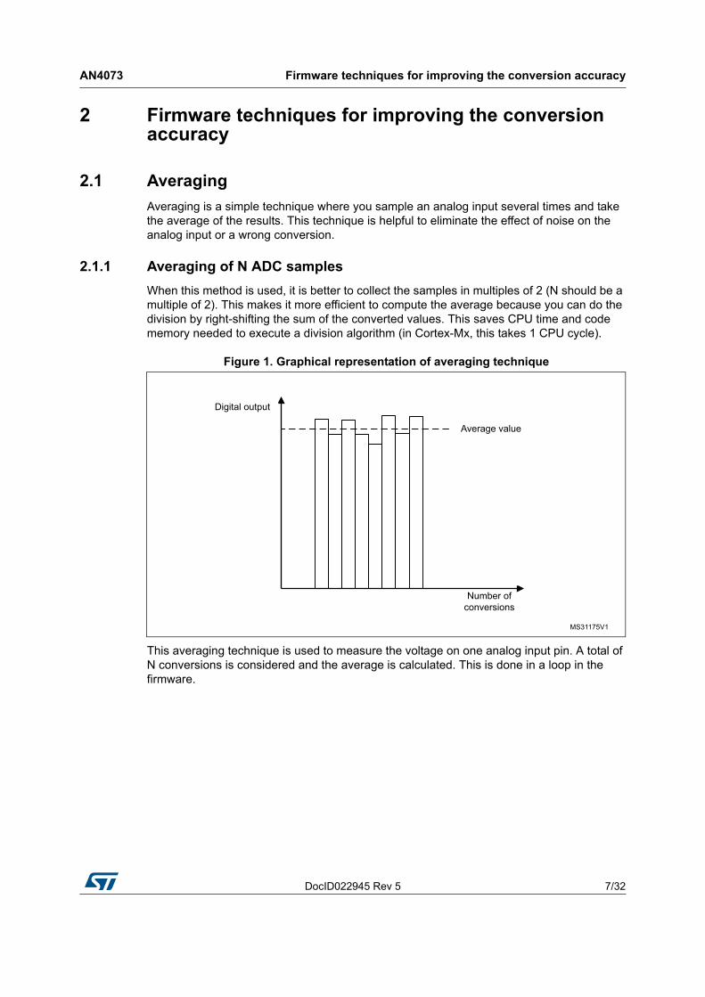
2.1 Averaging
Averaging is a simple technique where you sample an analog input several times and take the average of the results. This technique is helpful to eliminate the effect of noise on the analog input or a wrong conversion.
2.1.1 Averaging of N ADC samples
When this method is used, it is better to collect the samples in multiples of 2 (N should be a multiple of 2). This makes it more efficient to compute the average because you can do the division by right-shifting the sum of the converted values. This saves CPU time and code memory needed to execute a division algorithm (in Cortex-Mx, this takes 1 CPU cycle).
Figure 1. Graphical representation of averaging technique
This averaging technique is used to measure the voltage on one analog input pin. A total of N conversions is considered and the average is calculated. This is done in a loop in the firmware.
MS31175V1
Digital output
Average value
Number of conversions
Firmware techniques for improving the conversion accuracy AN4073
8/32 DocID022945 Rev 5
Figure 2. Averaging of N sample algorithm
Total conversion time = (number of samples * ADC conversion time) + computation time.
Computation time = time taken to read the results, add them together and calculate the average by dividing the total by the number of samples.
There is a trade-off between the total conversion time and the number of samples used to average, depending on the analog signal variations and the time available for computation.
Note: Refer to Appendix A for more details about the code source used.
2.1.2 Averaging of N-X ADC samples
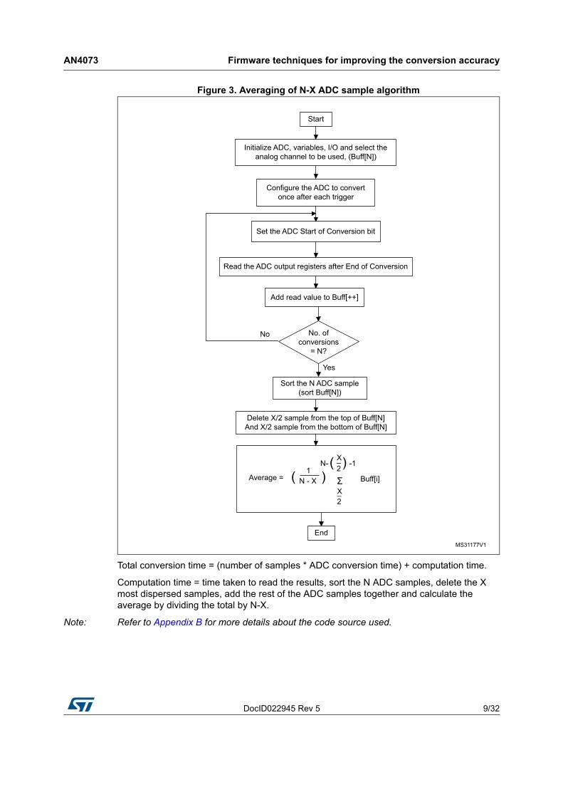
This method is based on taking N ADC samples, sorting them from the highest to the lowest value (or the reverse) and deleting the dispersed X samples.
It is recommended to choose N and X as multiples of 2.
This averaging method is more efficient than the previous one, as it deletes the most dispersed values which could impact the average, and it gives a good trade-off between the execution time and the conversion accuracy.
MS31176V1
Start
Initialize ADC, variables, I/O and select the analog channel to be used, (Total=0)
Configure the ADC to convert once after each trigger
Set the ADC Start of Conversion bit
Read the ADC output registers after End of Conversion
Add read value to Total
No. of conversions
= N?
Average = Total / N
End
Yes
No
DocID022945 Rev 5 9/32
AN4073 Firmware techniques for improving the conversion accuracy
31
Figure 3. Averaging of N-X ADC sample algorithm
Total conversion time = (number of samples * ADC conversion time) + computation time.
Computation time = time taken to read the results, sort the N ADC samples, delete the X most dispersed samples, add the rest of the ADC samples together and calculate the average by dividing the total by N-X.
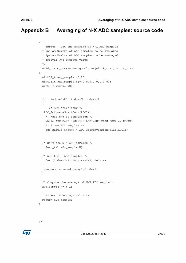
Note: Refer to Appendix B for more details about the code source used.
MS31177V1
Start
Initialize ADC, variables, I/O and select the analog channel to be used, (Buff[N])
Configure the ADC to convert once after each trigger
Set the ADC Start of Conversion bit
Read the ADC output registers after End of Conversion
Add read value to Buff[++]
No. of conversions
= N?
Sort the N ADC sample (sort Buff[N])
End
Yes
No
Delete X/2 sample from the top of Buff[N]And X/2 sample from the bottom of Buff[N]
N- _2X
-1( )
_2X
Buff[i]( )N - X1
Average =
Firmware techniques for improving the conversion accuracy AN4073
10/32 DocID022945 Rev 5
2.2 Additional recommendation
ADC conversion results are the ratio of the input voltage to the reference voltage. If there is noise in the reference voltage, then the results may not be accurate. Both hardware and firmware design are responsible for reducing the noise.
The execution of code generates some non-negligible noise on the internal power supply network of the microcontroller. To filter this noise, the VDDA (or VREF) and VSSA analog supply pins are available on the microcontroller package; you can connect a capacitor filter to these power supply pins to filter a high frequency noise.
Here are some general firmware design tips for reducing system noise in order to achieve a better ADC conversion accuracy:
1. Avoid starting transmission on any communication peripheral just before starting the ADC conversion. The toggling of the I/Os may create some noise in the supply voltage.
2. Avoid toggling high-sink I/Os which cause noise ripples in the power supply.
3. Avoid toggling digital outputs on the same I/O port as the A/D input is being converted. This can introduce switching noise into the analog inputs.
4. It is recommended to configure the STM32F2/F4 ART with data cache + Instruction cache enable and to disable the prefetch. This will avoid extra CPU accesses to the Flash memory causing an additional noise which can significantly decrease the ADC accuracy in some applications.
DocID022945 Rev 5 11/32
AN4073 STM32F2 and STM32F4 practical measurements
31
3 STM32F2 and STM32F4 practical measurements
This section only applies to all STM32F2xx, STM32F405, STM32F415, STM32F407 and STM32F417 microcontrollers.
This section gives some ADC accuracy measurements, putting the previously described methods into practice.
3.1 Measurement conditions
3.1.1 Hardware setup
STM32F407ZGT6 soldered on a test board (with only a minimum number of other hardware components)
Ambient temperature: 25°C
3 power supplies are applied to the MCU: VDD/VSS, VDDA/VSSA, VREF+/VREF-
Power supply range: VDD=VDDA=VREF+ = 3.3 V, fADC = 36 MHz
Clock source: external clock (8 MHz) provided by a generator, PLL is enabled, fCPU = 144 MHz
Three fixed analog input voltages are tested: 0.3 V, 1.65 V and 3 V
3.1.2 Firmware setup
ADC channel 2 is used in single conversion mode
50000 acquisitions were taken for each fixed analog input voltage
Five firmware methods were used to examine the ADC converted data:
– Raw data (without averaging)
– Averaging of 4 ADC samples
– Averaging of 6 ADC samples
– Averaging of 8 ADC samples
– Averaging of 8 ADC samples and deleting the 4 most dispersed samples
Note: All tests were done with fADC = 36 MHz, sampling time = 3 ADC cycles and ADC resolution = 12 bits in order to achieve the fastest ADC conversion (2.4 Msps).
3.2 Results
These measurements have been done based on a characterization of the ADC and are confirmed by further investigations (about 100 tests), where many parameters were evaluated to analyze the impact of each one.
The following measurements were considered while evaluating the impact of three different ART configurations on the ADC accuracy:
ART ON: (data cache + instruction cache + prefetch) ON
ART OFF: (data cache + instruction cache + prefetch) OFF
(Data cache + instruction cache) ON + prefetch OFF
STM32F2 and STM32F4 practical measurements AN4073
12/32 DocID022945 Rev 5
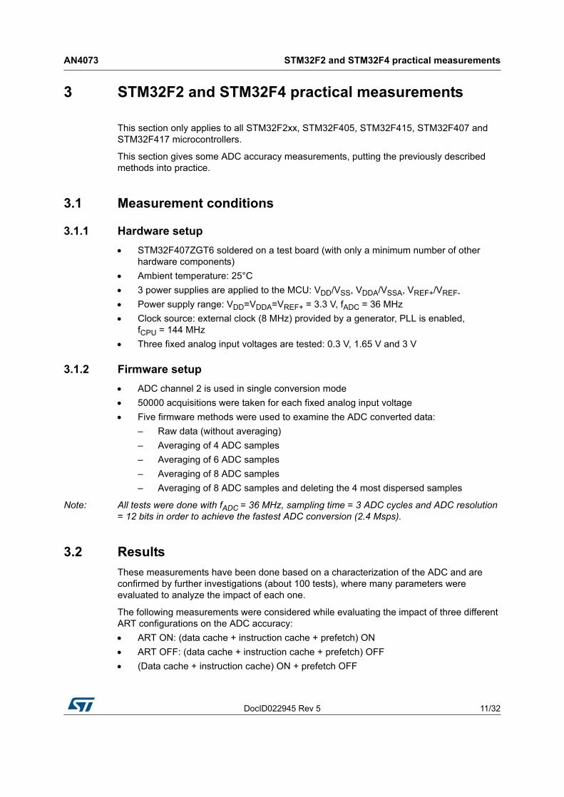
Note: All results are evaluated versus a dispertion range of +-5 LSB around the value which occurred the most in the histogram (see Figure 4).
Figure 4. Histogram graphical representation versus code dispersion
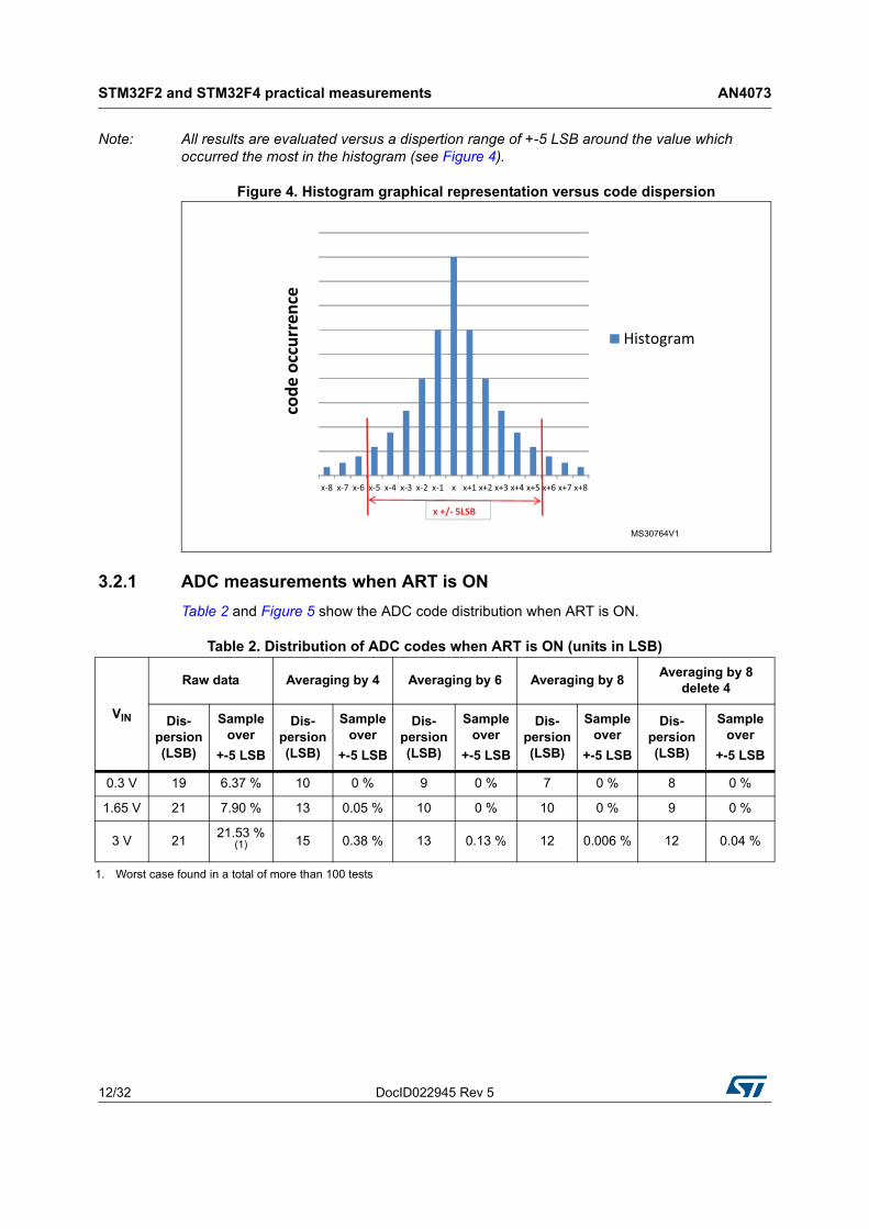
3.2.1 ADC measurements when ART is ON
Table 2 and Figure 5 show the ADC code distribution when ART is ON.
x-8 x-7 x-6 x-5 x-4 x-3 x-2 x-1 x x+1 x+2 x+3 x+4 x+5 x+6 x+7 x+8
code
occ
urre
nce
Histogram
x +/- 5LSB
MS30764V1
Table 2. Distribution of ADC codes when ART is ON (units in LSB)
VIN
Raw data Averaging by 4 Averaging by 6 Averaging by 8Averaging by 8
delete 4
Dis-persion (LSB)
Sample over
+-5 LSB
Dis-persion (LSB)
Sample over
+-5 LSB
Dis-persion (LSB)
Sample over
+-5 LSB
Dis-persion (LSB)
Sample over
+-5 LSB
Dis-persion (LSB)
Sample over
+-5 LSB
0.3 V 19 6.37 % 10 0 % 9 0 % 7 0 % 8 0 %
1.65 V 21 7.90 % 13 0.05 % 10 0 % 10 0 % 9 0 %
3 V 2121.53 %
(1) 15 0.38 % 13 0.13 % 12 0.006 % 12 0.04 %
1. Worst case found in a total of more than 100 tests
DocID022945 Rev 5 13/32
AN4073 STM32F2 and STM32F4 practical measurements
31
Figure 5. Distribution of ADC codes when ART is ON and VIN = 0.3 V
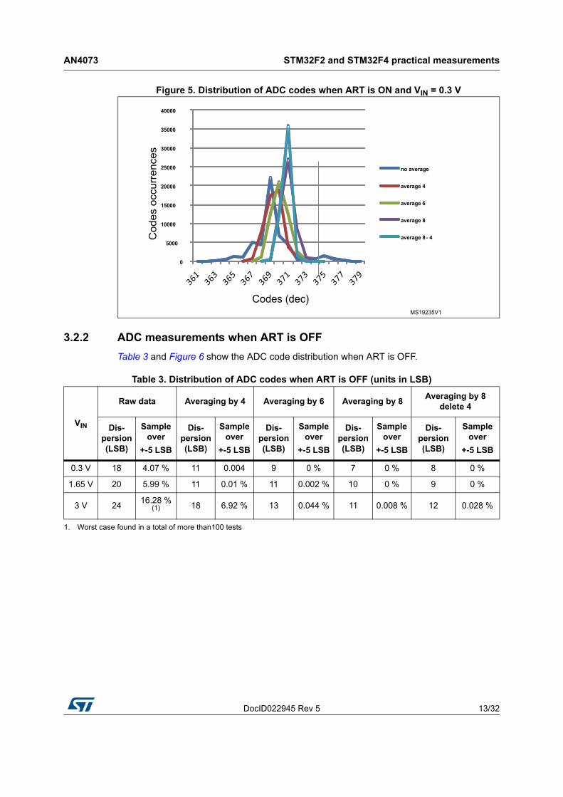
3.2.2 ADC measurements when ART is OFF
Table 3 and Figure 6 show the ADC code distribution when ART is OFF.
0
5000
10000
15000
20000
25000
30000
35000
40000
Codes (dec)
no average
average 4
average 6
average 8
average 8 - 4Cod
es o
ccur
renc
es
MS19235V1
Table 3. Distribution of ADC codes when ART is OFF (units in LSB)
VIN
Raw data Averaging by 4 Averaging by 6 Averaging by 8Averaging by 8
delete 4
Dis-persion (LSB)
Sample over
+-5 LSB
Dis-persion (LSB)
Sample over
+-5 LSB
Dis-persion (LSB)
Sample over
+-5 LSB
Dis-persion (LSB)
Sample over
+-5 LSB
Dis-persion (LSB)
Sample over
+-5 LSB
0.3 V 18 4.07 % 11 0.004 9 0 % 7 0 % 8 0 %
1.65 V 20 5.99 % 11 0.01 % 11 0.002 % 10 0 % 9 0 %
3 V 2416.28 %
(1) 18 6.92 % 13 0.044 % 11 0.008 % 12 0.028 %
1. Worst case found in a total of more than100 tests
STM32F2 and STM32F4 practical measurements AN4073
14/32 DocID022945 Rev 5
Figure 6. Distribution of ADC codes when ART is OFF and VIN = 1.65 V
MS19236V1
0
5000
10000
15000
20000
25000
30000
35000
40000
no average
average 4
average 6
average 8
average 8 - 4
Code
s occ
urre
nces
Codes (dec)
DocID022945 Rev 5 15/32
AN4073 STM32F2 and STM32F4 practical measurements
31
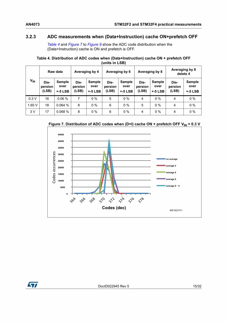
3.2.3 ADC measurements when (Data+Instruction) cache ON+prefetch OFF
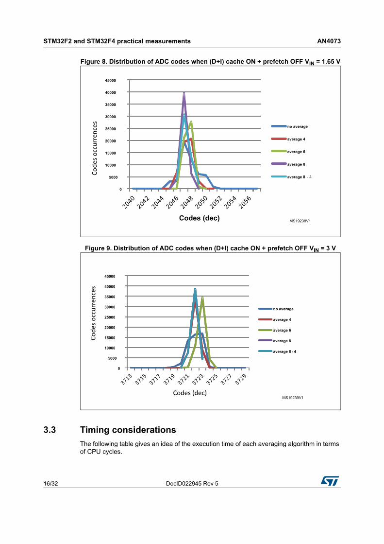
Table 4 and Figure 7 to Figure 9 show the ADC code distribution when the (Data+Instruction) cache is ON and prefetch is OFF.
Figure 7. Distribution of ADC codes when (D+I) cache ON + prefetch OFF VIN = 0.3 V
Table 4. Distribution of ADC codes when (Data+Instruction) cache ON + prefetch OFF(units in LSB)
VIN
Raw data Averaging by 4 Averaging by 6 Averaging by 8Averaging by 8
delete 4
Dis-persion (LSB)
Sample over
+-5 LSB
Dis-persion (LSB)
Sample over
+-5 LSB
Dis-persion (LSB)
Sample over
+-5 LSB
Dis-persion (LSB)
Sample over
+-5 LSB
Dis-persion (LSB)
Sample over
+-5 LSB
0.3 V 16 0.06 % 7 0 % 5 0 % 4 0 % 4 0 %
1.65 V 18 0.064 % 8 0 % 6 0 % 5 0 % 4 0 %
3 V 17 0.068 % 8 0 % 6 0 % 4 0 % 4 0 %
Code
s occ
urre
nces
MS19237V1
0
5000
10000
15000
20000
25000
30000
35000
40000
45000
Codes (dec)
no average
average 4
average 6
average 8
average 8 - 4
STM32F2 and STM32F4 practical measurements AN4073
16/32 DocID022945 Rev 5
Figure 8. Distribution of ADC codes when (D+I) cache ON + prefetch OFF VIN = 1.65 V
Figure 9. Distribution of ADC codes when (D+I) cache ON + prefetch OFF VIN = 3 V
3.3 Timing considerations
The following table gives an idea of the execution time of each averaging algorithm in terms of CPU cycles.
Code
s occ
urre
nces
MS19238V1
0
5000
10000
15000
20000
25000
30000
35000
40000
45000
Codes (dec)
no average
average 4
average 6
average 8
average 8 - 4
Code
s occ
urre
nces
MS19239V1
0
5000
10000
15000
20000
25000
30000
35000
40000
45000
Codes (dec)
no average
average 4
average 6
average 8
average 8 - 4
DocID022945 Rev 5 17/32
AN4073 STM32F2 and STM32F4 practical measurements
31
Note: These timing measurements are considered based on the optimum ART configuration: (Data+Instruction) cache ON, Prefetch OFF, which results in the best ADC noise immunity.
In other ART configurations, these measurements could result in a difference of a few cycles.
Note: Please note that the time required to get N samples = N * (tSAMPLING + tCONVERSION)
3.4 Measurement conclusion
Following the previous results, we can conclude that, in order to obtain the most accurate conversion results when using the STM32F2/F405/F415/F407/F417 ADC, care must be taken to configure the ART Flash memory accelerator accordingly. This configuration must be (Data+Instruction) ON and prefetch OFF to achieve the best accuracy by limiting the internal noise generated by the Flash.
This section shows how you can choose the best trade-off between A/D conversion accuracy and the required A/D conversion speed.
For example, the measurements given above demonstrate that, with a 12-bit ADC resolution, +- 5 LSB can be achieved using an averaging by 4 algorithm (0.6 Msps) when the ART Flash memory accelerator is configured with (Data+Instruction) ON and prefetch OFF.
Table 5. Time needed to compute averaging
Computation time
Averaging by 4 (1)
1. Computation = time taken to add the N samples and divide them by N.
Averaging by 6 (1) Averaging by 8 (1) Averaging by 8, delete 4 (2)
2. Computation = time taken to sort the 8 ADC samples, delete the 4 dispersed ones, add the other 4 samples and divide them by 4. This result depends on the sorting algorithm (in this case, the sorting algorithm is based on successive permutation, which is not optimized for speed).
CPU cycles(3)
3. CPU frequency is 144 MHz, as described in Section 3.1.1.
18 26 36 517
STM32F4 ADC accuracy options AN4073
18/32 DocID022945 Rev 5
4 STM32F4 ADC accuracy options
This section only applies to STM32F42x/F43x microcontrollers.
Before describing the STM32F42x and STM32F43x ADC evaluation results, the silicon configurable options embedded on these products to enhance the ADC accuracy will be detailed.
4.1 Configuration options for ADC accuracy
By default, on these products, noise filtering techniques are activated internally between the ADC analog block and other microcontroller blocks. These techniques will reduce the power supply noise, the signal crosstalk and the EMI-induced noise. For more details about practical ADC results in this condition, please refer to section 4.2.3.
To further improve the ADC accuracy, two configurable options are available. The following names are used throughout the document:
Default: The default STM32 configuration which is always active out of reset.
Option 1: The first configurable option which can be activated by firmware.
Option 2: The second configurable option which can be activated by firmware.
4.1.1 Option 1
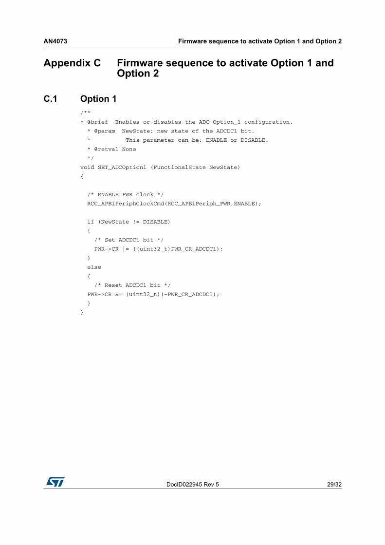
This option can be activated or not by firmware.
By default, it is not active. When activated by firmware, it continuously masks the extra flash access generated by the prefetch mechanism which can produce random noise impacting the ADC accuracy.
This could be activated by setting the ADCDC1 (bit 13) in the PWR_CR register.
Warning: This bit can only be set at the following conditions: - Prefetch must be OFF.- VDD voltage ranges from 2.4 V to 3.6 V.- This bit must not be set when the ADCxDC2 bit in SYSCFG_PMC register is set.
For more details about the exact firmware sequence to enable Option 1, please refer to Section C.1: Option 1.
The ADC accuracy results when activating this option, will be detailed in next section.
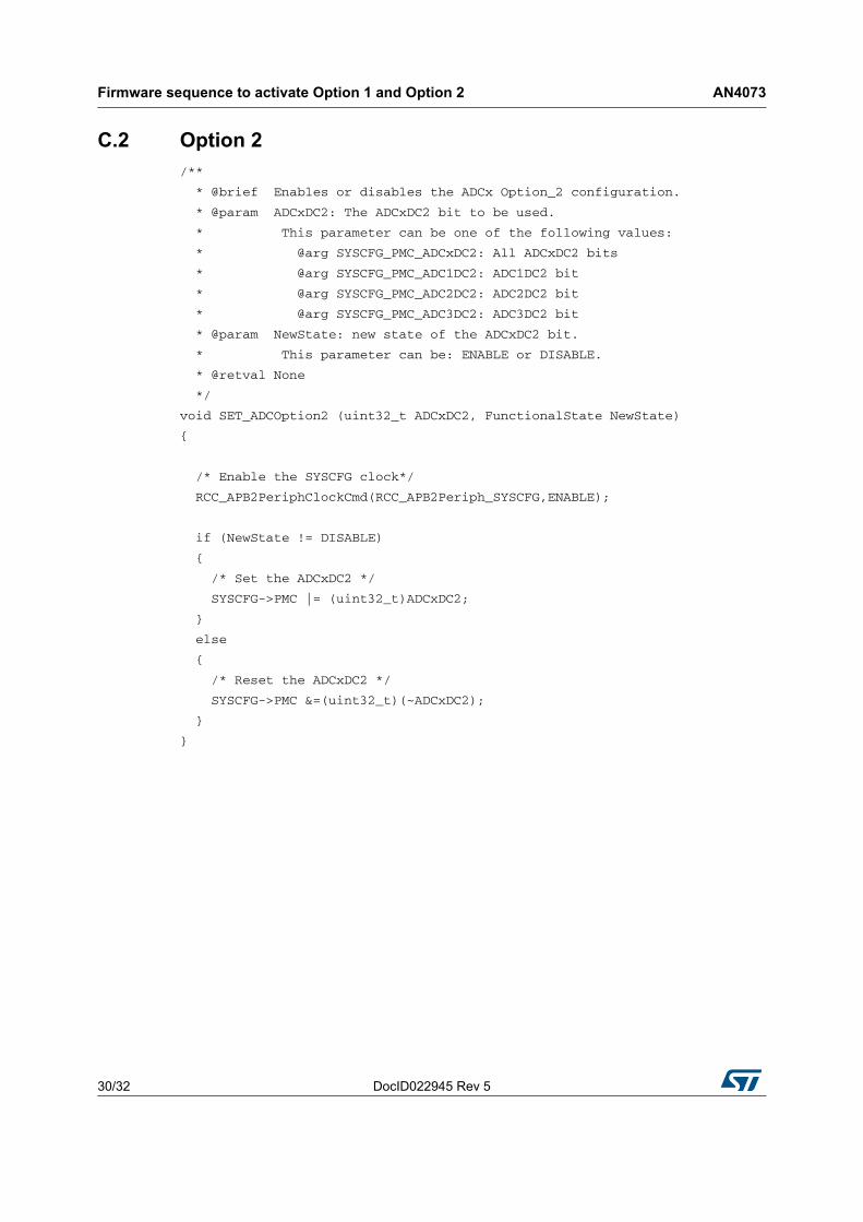
4.1.2 Option 2
This option can be activated or not by firmware.
By default, it is not active. When activated by firmware, it masks the internal flash noise during the last ADC sampling cycle. This will improve the ADC immunity versus internal spurious flash noise.
DocID022945 Rev 5 19/32
AN4073 STM32F4 ADC accuracy options
31
This could be activated by setting the ADCxDC2 (bit 16 - bit18) in the SYSCFG_PMC register.
Warning: These bits can only be set at the following conditions: - Minimum ADC clock is 30MHz.- Only one ADCxDC2 bit must be selected in case ADC conversion does not start at the same time and different sampling times are used.- ADC resolution should be equal to 12 bits.- This bit must not be set when the ADCDC1 bit in PWR_CR register is set.
In this option, one bit for each ADC is available in SYSCFG_PMC register. There is more flexibility to enable or not this option for each ADC separately.
As stated in the warning above, these three bits should not be activated simultaneously in some conditions.
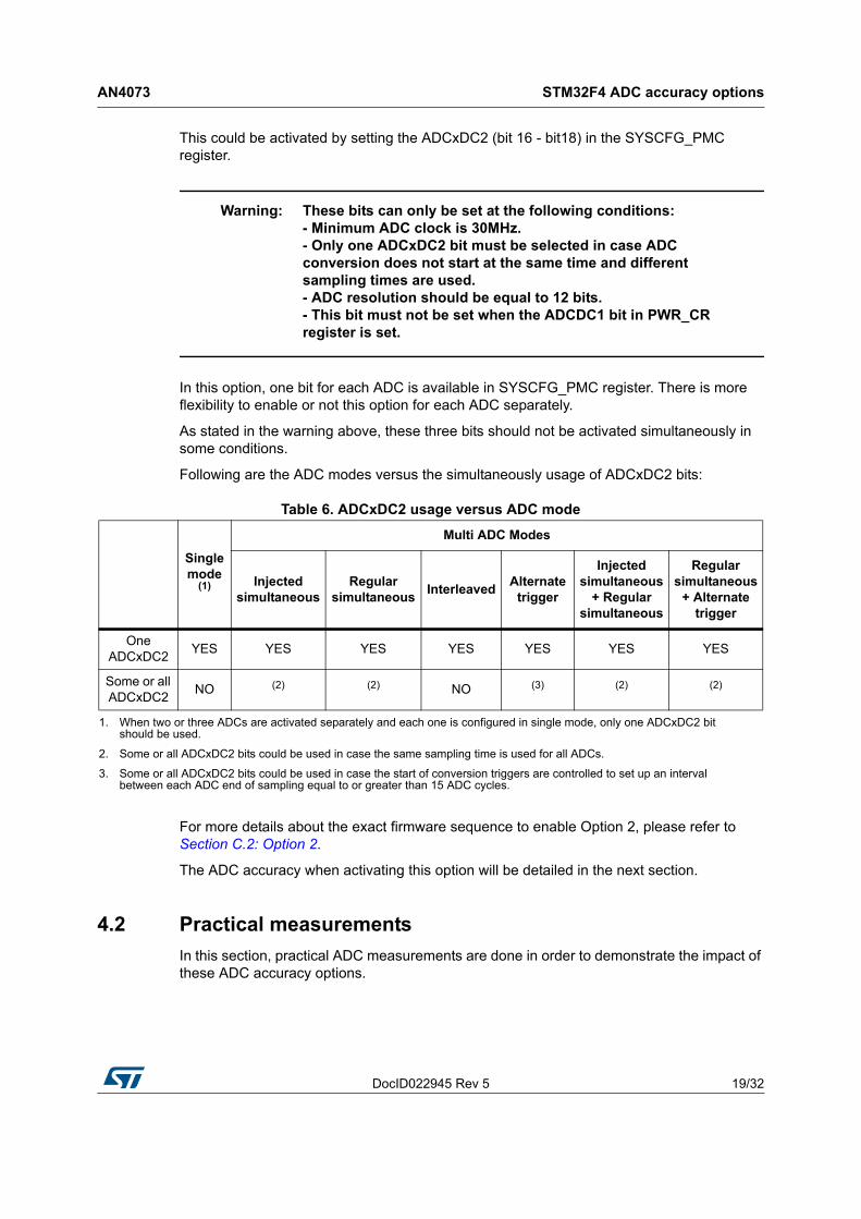
Following are the ADC modes versus the simultaneously usage of ADCxDC2 bits:
For more details about the exact firmware sequence to enable Option 2, please refer to Section C.2: Option 2.
The ADC accuracy when activating this option will be detailed in the next section.
4.2 Practical measurements
In this section, practical ADC measurements are done in order to demonstrate the impact of these ADC accuracy options.
Table 6. ADCxDC2 usage versus ADC mode
Single mode
(1)
Multi ADC Modes
Injected simultaneous
Regular simultaneous
Interleaved Alternate
trigger
Injected simultaneous
+ Regular simultaneous
Regular simultaneous
+ Alternate trigger
One ADCxDC2
YES YES YES YES YES YES YES
Some or all ADCxDC2
NO (2) (2) NO (3) (2) (2)
1. When two or three ADCs are activated separately and each one is configured in single mode, only one ADCxDC2 bit should be used.
2. Some or all ADCxDC2 bits could be used in case the same sampling time is used for all ADCs.
3. Some or all ADCxDC2 bits could be used in case the start of conversion triggers are controlled to set up an interval between each ADC end of sampling equal to or greater than 15 ADC cycles.
STM32F4 ADC accuracy options AN4073
20/32 DocID022945 Rev 5
4.2.1 Hardware Setup
The hardware environment used for the ADC tests is the same as the one described in Section 3.1.1: Hardware setup, with the use of STM32F43x.
4.2.2 Common firmware setup
ADC1 Channel 1 is used in single conversion mode,
The sampling time is fixed to 3 ADC clock cycles,
50000 acquisition was taken for each fixed analog input voltage,
All tests are done with FADC = 36 MHz, sampling time= 3 ADC cycles and ADC resolution = 12 bits in order to achieve the fastest ADC conversion which is equal to 2.4 MSPS.
4.2.3 Results
The following measurements were taken while evaluating the impact of the ADC accuracy options embedded on these products at three different ART configurations which are:
ART ON: (data cache + instruction cache + prefetch) ON,
ART OFF: (data cache + instruction cache + prefetch) OFF,
(Data cache + instruction cache) ON + Prefetch OFF
1. ADC measurements when ART is ON
The following table and graph show the ADC code distribution when ART is ON at two different conditions: Default STM32 configuration and when Option 2 is active:
Table 7. Distribution of ADC codes when ART is ON
VIN
Default Option 1 Option 2
Dispersion (LSB)
sample over +-5 LSB
Dispersion (LSB)
sample over +-5
LSB
Dispersion (LSB)
sample over +-5 LSB
0.3 V 7 0%
(1)
1. Option 1 is not applicable since Prefetch is ON in this case.
4 0%
1.65 V 9 0% 6 0%
3 V 7 0% 6 0%
DocID022945 Rev 5 21/32
AN4073 STM32F4 ADC accuracy options
31
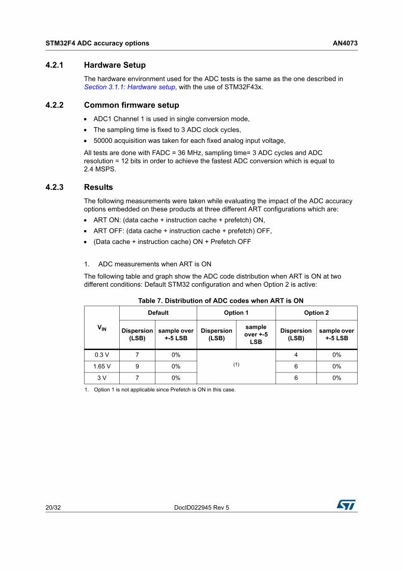
Figure 10. Distribution of ADC codes when ART is ON and VIN = 0.3 V
In the same conditions, when ART is ON, using the default STM32 configuration with STM32F2xx or STM32F405/F415/F407/F417 would give a maximum dispersion of 21 LSB (refer to Table 2) while, in this case, the maximum dispersion is 9 LSB.
This confirms that the default STM32 configuration embedded on these products allows to achieve about 50 % of dispersion code versus STM32F2xx/F405/F415/F407/F417, and about 75 % when Option 2 is active.
2. ADC measurements when ART is OFF
The following table and graph show the ADC code distribution when ART is OFF at three different conditions: Default STM32 configuration, Option 1 and Option 2 are active.
Table 8. Distribution of ADC codes when ART is OFF
VIN
Default Option 1 Option 2
Dispersion (LSB)
sample over +-5 LSB
Dispersion (LSB)
sample over +5 LSB
Dispersion (LSB)
sample over +- 5 LSB
0.3 V 9 0% 5 0% 5 0%
1.65 V 10 0% 7 0% 7 0%
3 V 8 0% 6 0% 6 0%
0
5000
10000
15000
20000
25000
30000
371 372 373 374 375 376 377
code
occ
uren
ce
code (dec)
DefaultOption 2
MS30758V1
STM32F4 ADC accuracy options AN4073
22/32 DocID022945 Rev 5
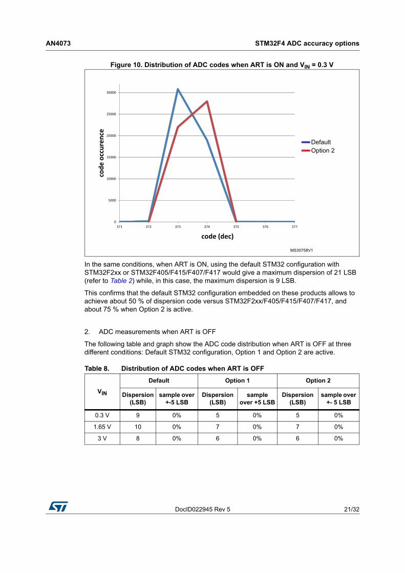
Figure 11. Distribution of ADC codes when ART is OFF and VIN = 1.65 V
In the same conditions, when ART is OFF, using the Default STM32 configuration with STM32F2xx or STM32F405/F415/F407/F417 gives a maximum dispersion of 24 LSB (refer to Table 3) while, in this case, the maximum dispersion is 10 LSB.
This confirms that the default STM32 configuration embedded on these products allows to achieve more than 50 % of dispersion code versus STM32F2xx/F405/F415/F407/F417, and about 75 % when one of the options is active.
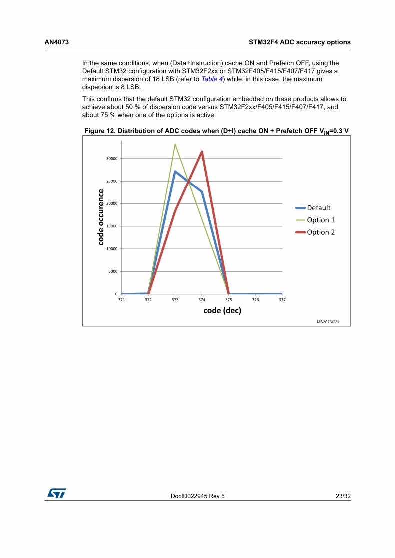
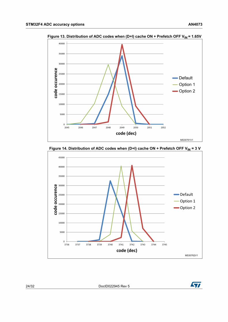
3. ADC measurements when (Data+Instruction) cache ON + Prefetch OFF
The following table and graph show the ADC code distribution when (Data + Instruction) cache ON and prefetch OFF at three different conditions: default STM32 configuration, Option 1 and Option 2 are active.
0
5000
10000
15000
20000
25000
30000
2044 2045 2046 2047 2048 2049 2050 2051 2052 2053
code
occ
uren
ce
code (dec)
DefaultOption 1Option 2
MS30759V1
Table 9. Distribution of ADC codes when (Data+Instruction) cache ON + prefetch OFF
VIN
Default Option 1 Option 2
Dispersion (LSB)
sample over +-5 LSB
Dispersion (LSB)
sample over +-5 LSB
Dispersion (LSB)
sample over +-5 LSB
0.3 V 7 0% 4 0% 4 0%
1.65 V 8 0% 6 0% 6 0%
3 V 7 0% 6 0% 7 0%
DocID022945 Rev 5 23/32
AN4073 STM32F4 ADC accuracy options
31
In the same conditions, when (Data+Instruction) cache ON and Prefetch OFF, using the Default STM32 configuration with STM32F2xx or STM32F405/F415/F407/F417 gives a maximum dispersion of 18 LSB (refer to Table 4) while, in this case, the maximum dispersion is 8 LSB.
This confirms that the default STM32 configuration embedded on these products allows to achieve about 50 % of dispersion code versus STM32F2xx/F405/F415/F407/F417, and about 75 % when one of the options is active.
Figure 12. Distribution of ADC codes when (D+I) cache ON + Prefetch OFF VIN=0.3 V
0
5000
10000
15000
20000
25000
30000
371 372 373 374 375 376 377
code
occ
uren
ce
code (dec)
DefaultOption 1Option 2
MS30760V1
STM32F4 ADC accuracy options AN4073
24/32 DocID022945 Rev 5
Figure 13. Distribution of ADC codes when (D+I) cache ON + Prefetch OFF VIN = 1.65V
Figure 14. Distribution of ADC codes when (D+I) cache ON + Prefetch OFF VIN = 3 V
0
5000
10000
15000
20000
25000
30000
35000
40000
2045 2046 2047 2048 2049 2050 2051 2052
code
occ
uren
ce
code (dec)
DefaultOption 1Option 2
MS30761V1
0
5000
10000
15000
20000
25000
30000
35000
40000
45000
3736 3737 3738 3739 3740 3741 3742 3743 3744 3745
code
occ
uren
ce
code (dec)
DefaultOption 1Option 2
MS30762V1
DocID022945 Rev 5 25/32
AN4073 STM32F4 ADC accuracy options
31
4.3 Measurement conclusions
Based on these measurements and comparing to STM32F2xx and STM32F405/F415/F407/ F417 measurements, we can conclude that ADC accuracy options embedded on these products allow an improvement of the ADC code dispersion up to 75 %.
For the applicable products, you can choose either to work with the default configuration or to enable one of the options; It depends on the ADC precision required by the application.
Based on these typical measurements, to achieve the best ADC accuracy with these products, you need to know that:
For the Default configuration: Prefetch OFF + Data cache ON + Instruction cache ON gives a maximum of 8 codes of dispersion.
When activating Option 1: Prefetch OFF + Data cache ON + Instruction cache ON gives a maximum of 6 codes of dispersion.
When activating Option 2: Prefetch ON + Data cache ON + Instruction cache ON gives a maximum of 6 codes of dispersion.
However, Options 1 and 2 should only be applied in specific conditions as detailed above (refer to Section 4.1) to avoid any MCU malfunction.
Averaging of N ADC samples: source code AN4073
26/32 DocID022945 Rev 5
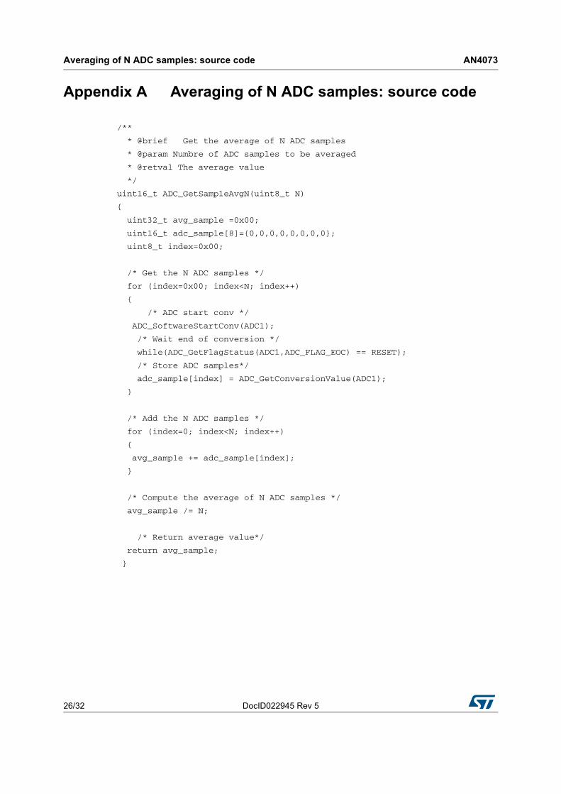
Appendix A Averaging of N ADC samples: source code
/**
* @brief Get the average of N ADC samples
* @param Numbre of ADC samples to be averaged
* @retval The average value
*/
uint16_t ADC_GetSampleAvgN(uint8_t N)
{
uint32_t avg_sample =0x00;
uint16_t adc_sample[8]={0,0,0,0,0,0,0,0};
uint8_t index=0x00;
/* Get the N ADC samples */
for (index=0x00; index<N; index++)
{
/* ADC start conv */
ADC_SoftwareStartConv(ADC1);
/* Wait end of conversion */
while(ADC_GetFlagStatus(ADC1,ADC_FLAG_EOC) == RESET);
/* Store ADC samples*/
adc_sample[index] = ADC_GetConversionValue(ADC1);
}
/* Add the N ADC samples */
for (index=0; index<N; index++)
{
avg_sample += adc_sample[index];
}
/* Compute the average of N ADC samples */
avg_sample /= N;
/* Return average value*/
return avg_sample;
}
DocID022945 Rev 5 27/32
AN4073 Averaging of N-X ADC samples: source code
31
Appendix B Averaging of N-X ADC samples: source code
/**
* @brief Get the average of N-X ADC samples
* @param Numbre of ADC samples to be averaged
* @param Numbre of ADC samples to be averaged
* @retval The average value
*/
uint16_t ADC_GetSampleAvgNDeleteX(uint8_t N , uint8_t X)
{
uint32_t avg_sample =0x00;
uint16_t adc_sample[8]={0,0,0,0,0,0,0,0};
uint8_t index=0x00;
for (index=0x00; index<N; index++)
{
/* ADC start conv */
ADC_SoftwareStartConv(ADC1);
/* Wait end of conversion */
while(ADC_GetFlagStatus(ADC1,ADC_FLAG_EOC) == RESET);
/* Store ADC samples */
adc_sample[index] = ADC_GetConversionValue(ADC1);
}
/* Sort the N-X ADC samples */
Sort_tab(adc_sample,N);
/* Add the N ADC samples */
for (index=X/2; index<N-X/2; index++)
{
avg_sample += adc_sample[index];
}
/* Compute the average of N-X ADC sample */
avg_sample /= N-X;
/* Return average value */
return avg_sample;
}
/**
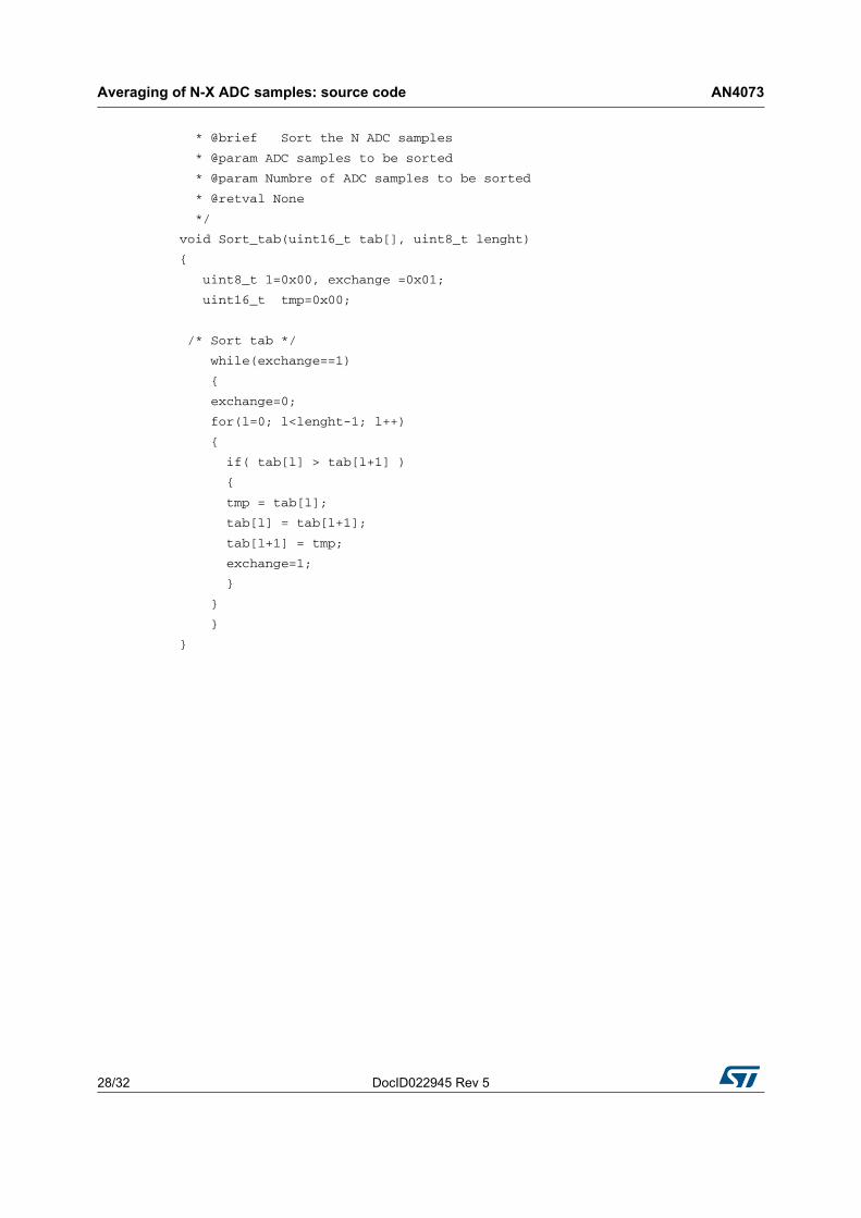
Averaging of N-X ADC samples: source code AN4073
28/32 DocID022945 Rev 5
* @brief Sort the N ADC samples
* @param ADC samples to be sorted
* @param Numbre of ADC samples to be sorted
* @retval None
*/
void Sort_tab(uint16_t tab[], uint8_t lenght)
{
uint8_t l=0x00, exchange =0x01;
uint16_t tmp=0x00;
/* Sort tab */
while(exchange==1)
{
exchange=0;
for(l=0; l<lenght-1; l++)
{
if( tab[l] > tab[l+1] )
{
tmp = tab[l];
tab[l] = tab[l+1];
tab[l+1] = tmp;
exchange=1;
}
}
}
}
DocID022945 Rev 5 29/32
AN4073 Firmware sequence to activate Option 1 and Option 2
31
Appendix C Firmware sequence to activate Option 1 and Option 2
C.1 Option 1
/**
* @brief Enables or disables the ADC Option_1 configuration.
* @param NewState: new state of the ADCDC1 bit.
* This parameter can be: ENABLE or DISABLE.
* @retval None
*/
void SET_ADCOption1 (FunctionalState NewState)
{
/* ENABLE PWR clock */
RCC_APB1PeriphClockCmd(RCC_APB1Periph_PWR,ENABLE);
if (NewState != DISABLE)
{
/* Set ADCDC1 bit */
PWR->CR |= ((uint32_t)PWR_CR_ADCDC1);
}
else
{
/* Reset ADCDC1 bit */
PWR->CR &= (uint32_t)(~PWR_CR_ADCDC1);
}
}
Firmware sequence to activate Option 1 and Option 2 AN4073
30/32 DocID022945 Rev 5
C.2 Option 2
/**
* @brief Enables or disables the ADCx Option_2 configuration.
* @param ADCxDC2: The ADCxDC2 bit to be used.
* This parameter can be one of the following values:
* @arg SYSCFG_PMC_ADCxDC2: All ADCxDC2 bits
* @arg SYSCFG_PMC_ADC1DC2: ADC1DC2 bit
* @arg SYSCFG_PMC_ADC2DC2: ADC2DC2 bit
* @arg SYSCFG_PMC_ADC3DC2: ADC3DC2 bit
* @param NewState: new state of the ADCxDC2 bit.
* This parameter can be: ENABLE or DISABLE.
* @retval None
*/
void SET_ADCOption2 (uint32_t ADCxDC2, FunctionalState NewState)
{
/* Enable the SYSCFG clock*/
RCC_APB2PeriphClockCmd(RCC_APB2Periph_SYSCFG,ENABLE);
if (NewState != DISABLE)
{
/* Set the ADCxDC2 */
SYSCFG->PMC |= (uint32_t)ADCxDC2;
}
else
{
/* Reset the ADCxDC2 */
SYSCFG->PMC &=(uint32_t)(~ADCxDC2);
}
}
DocID022945 Rev 5 31/32
AN4073 Revision history
31
Revision history
Table 10. Document revision history
Date Revision Changes
19-Mar-2012 1 Initial release.
21-Mar-2012 2 Inserted missing text on page 9.
10-Aug-2012 3
Replaced "STM32F20x, STM32F21x, STM32F40x and STM32F41x microcontrollers" by: "STM32F20x / STM32F21x (revZ, revY, revX) and STM32F40x/STM32F41x (revZ) microcontrollers" in the Introduction.
Added Appendix A: Averaging of N ADC samples: source code and Appendix B: Averaging of N-X ADC samples: source code, and corresponding notes in Section 2.1.1 and Section 2.1.2.
25-Feb-2013 4
Applied to STM32F2xx (STM32F20x, STM32F21x) and STM32F4xx (STM32F40x, STM32F41x, STM32F42x, STM32F43x) microcontrollers.
Section 3 now dedicated to STM32F2xx, STM32F405, STM32F415, STM32F407 and STM32F417 products, when new Section 4 is dedicated to STM32F42x/F43x products.
Added Appendix C: Firmware sequence to activate Option 1 and Option 2.
02-Jul-2013 5 Changed VDD range in warning in Section 4.1.1
AN4073
32/32 DocID022945 Rev 5
Please Read Carefully:
Information in this document is provided solely in connection with ST products. STMicroelectronics NV and its subsidiaries (“ST”) reserve theright to make changes, corrections, modifications or improvements, to this document, and the products and services described herein at anytime, without notice.
All ST products are sold pursuant to ST’s terms and conditions of sale.
Purchasers are solely responsible for the choice, selection and use of the ST products and services described herein, and ST assumes noliability whatsoever relating to the choice, selection or use of the ST products and services described herein.
No license, express or implied, by estoppel or otherwise, to any intellectual property rights is granted under this document. If any part of thisdocument refers to any third party products or services it shall not be deemed a license grant by ST for the use of such third party productsor services, or any intellectual property contained therein or considered as a warranty covering the use in any manner whatsoever of suchthird party products or services or any intellectual property contained therein.
UNLESS OTHERWISE SET FORTH IN ST’S TERMS AND CONDITIONS OF SALE ST DISCLAIMS ANY EXPRESS OR IMPLIEDWARRANTY WITH RESPECT TO THE USE AND/OR SALE OF ST PRODUCTS INCLUDING WITHOUT LIMITATION IMPLIEDWARRANTIES OF MERCHANTABILITY, FITNESS FOR A PARTICULAR PURPOSE (AND THEIR EQUIVALENTS UNDER THE LAWSOF ANY JURISDICTION), OR INFRINGEMENT OF ANY PATENT, COPYRIGHT OR OTHER INTELLECTUAL PROPERTY RIGHT.
ST PRODUCTS ARE NOT AUTHORIZED FOR USE IN WEAPONS. NOR ARE ST PRODUCTS DESIGNED OR AUTHORIZED FOR USEIN: (A) SAFETY CRITICAL APPLICATIONS SUCH AS LIFE SUPPORTING, ACTIVE IMPLANTED DEVICES OR SYSTEMS WITHPRODUCT FUNCTIONAL SAFETY REQUIREMENTS; (B) AERONAUTIC APPLICATIONS; (C) AUTOMOTIVE APPLICATIONS ORENVIRONMENTS, AND/OR (D) AEROSPACE APPLICATIONS OR ENVIRONMENTS. WHERE ST PRODUCTS ARE NOT DESIGNEDFOR SUCH USE, THE PURCHASER SHALL USE PRODUCTS AT PURCHASER’S SOLE RISK, EVEN IF ST HAS BEEN INFORMED INWRITING OF SUCH USAGE, UNLESS A PRODUCT IS EXPRESSLY DESIGNATED BY ST AS BEING INTENDED FOR “AUTOMOTIVE,AUTOMOTIVE SAFETY OR MEDICAL” INDUSTRY DOMAINS ACCORDING TO ST PRODUCT DESIGN SPECIFICATIONS.PRODUCTS FORMALLY ESCC, QML OR JAN QUALIFIED ARE DEEMED SUITABLE FOR USE IN AEROSPACE BY THECORRESPONDING GOVERNMENTAL AGENCY.
Resale of ST products with provisions different from the statements and/or technical features set forth in this document shall immediately voidany warranty granted by ST for the ST product or service described herein and shall not create or extend in any manner whatsoever, anyliability of ST.
ST and the ST logo are trademarks or registered trademarks of ST in various countries.Information in this document supersedes and replaces all information previously supplied.
The ST logo is a registered trademark of STMicroelectronics. All other names are the property of their respective owners.
© 2013 STMicroelectronics - All rights reserved
STMicroelectronics group of companies
Australia - Belgium - Brazil - Canada - China - Czech Republic - Finland - France - Germany - Hong Kong - India - Israel - Italy - Japan - Malaysia - Malta - Morocco - Philippines - Singapore - Spain - Sweden - Switzerland - United Kingdom - United States of America
www.st.com