Embed Size (px)
Citation preview
1
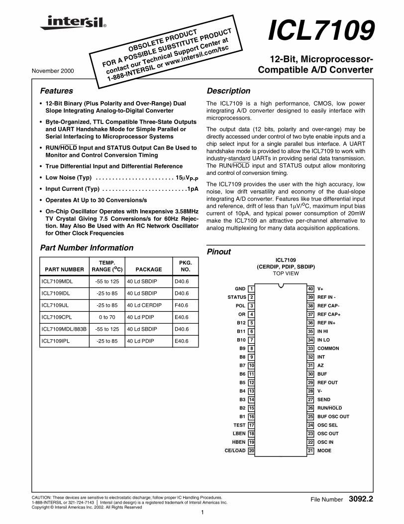
®
November 2000
ICL710912-Bit, Microprocessor-
Compatible A/D Converter
Features
• 12-Bit Binary (Plus Polarity and Over-Range) Dual Slope Integrating Analog-to-Digital Converter
• Byte-Organized, TTL Compatible Three-State Outputs and UART Handshake Mode for Simple Parallel or Serial Interfacing to Microprocessor Systems
• RUN/HOLD Input and STATUS Output Can Be Used to Monitor and Control Conversion Timing
• True Differential Input and Differential Reference
• Low Noise (Typ) . . . . . . . . . . . . . . . . . . . . . . . . 15µVP-P
• Input Current (Typ) . . . . . . . . . . . . . . . . . . . . . . . . . .1pA
• Operates At Up to 30 Conversions/s
• On-Chip Oscillator Operates with Inexpensive 3.58MHzTV Crystal Giving 7.5 Conversions/s for 60Hz Rejec-tion. May Also Be Used with An RC Network Oscillatorfor Other Clock Frequencies
Description
The ICL7109 is a high performance, CMOS, low powerintegrating A/D converter designed to easily interface withmicroprocessors.
The output data (12 bits, polarity and over-range) may bedirectly accessed under control of two byte enable inputs and achip select input for a single parallel bus interface. A UARThandshake mode is provided to allow the ICL7109 to work withindustry-standard UARTs in providing serial data transmission.The RUN/HOLD input and STATUS output allow monitoringand control of conversion timing.
The ICL7109 provides the user with the high accuracy, lownoise, low drift versatility and economy of the dual-slopeintegrating A/D converter. Features like true differential inputand reference, drift of less than 1µV/oC, maximum input biascurrent of 10pA, and typical power consumption of 20mWmake the ICL7109 an attractive per-channel alternative toanalog multiplexing for many data acquisition applications.
PinoutICL7109
(CERDIP, PDIP, SBDIP)TOP VIEW
Part Number Information
PART NUMBERTEMP.
RANGE (oC) PACKAGEPKG. NO.
ICL7109MDL -55 to 125 40 Ld SBDIP D40.6
ICL7109IDL -25 to 85 40 Ld SBDIP D40.6
ICL7109IJL -25 to 85 40 Ld CERDIP F40.6
ICL7109CPL 0 to 70 40 Ld PDIP E40.6
ICL7109MDL/883B -55 to 125 40 Ld SBDIP D40.6
ICL7109IPL -25 to 85 40 Ld PDIP E40.6
13
1
2
3
4
5
6
7
8
9
10
11
12
14
15
16
17
18
19
20
GND
STATUS
POL
OR
B12
B11
B10
B9
B8
B7
B6
B5
B4
B3
B2
B1
TEST
LBEN
HBEN
CE/LOAD
28
40
39
38
37
36
35
34
33
32
31
30
29
27
26
25
24
23
22
21
V+
REF IN -
REF CAP-
REF CAP+
REF IN+
IN HI
IN LO
COMMON
INT
AZ
BUF
REF OUT
V-
SEND
RUN/HOLD
BUF OSC OUT
OSC SEL
OSC OUT
OSC IN
MODE
File Number 3092.2CAUTION: These devices are sensitive to electrostatic discharge; follow proper IC Handling Procedures.1-888-INTERSIL or 321-724-7143 | Intersil (and design) is a registered trademark of Intersil Americas Inc.Copyright © Intersil Americas Inc. 2002. All Rights Reserved
FOR A POSSIBLE SUBSTITUTE PRODUCT
contact our Technical Support Center at
1-888-INTERSIL or www.intersil.com/tsc OBSOLETE PRODUCT
Absolute Maximum Ratings Thermal Information
Positive Supply Voltage (GND to V+). . . . . . . . . . . . . . . . . . . . +6.0VNegative Supply Voltage (GND to V-) . . . . . . . . . . . . . . . . . . . . . -9VAnalog Input Voltage (Either Input) (Note 1) . . . . . . . . . . . . V+ to V-Reference Input Voltage (Either Input) (Note 1) . . . . . . . . . . V+ to V-Digital Input Voltage . . . . . . . . . . . . . . . . . . . . . . . . . . . . . (V+) +0.3VPins 2-27 (Note 2) . . . . . . . . . . . . . . . . . . . . . . . . . . . . . .GND -0.3V
Operating ConditionsTemperature Range
M Suffix . . . . . . . . . . . . . . . . . . . . . . . . . . . . . . . . . -55oC to 125oCI Suffix . . . . . . . . . . . . . . . . . . . . . . . . . . . . . . . . . . . -25oC to 85oCC Suffix . . . . . . . . . . . . . . . . . . . . . . . . . . . . . . . . . . . .0oC to 75oC
Thermal Resistance (Typical, Note 1) θJA (oC/W) θJC (oC/W)SBDIP Package. . . . . . . . . . . . . . . . . . . . 60 20CERDIP Package . . . . . . . . . . . . . . . . . . 55 18PDIP Package . . . . . . . . . . . . . . . . . . . . . 50 N/A
Maximum Junction Temperature (PDIP Package) . . . . . . . . . 150oCMaximum Junction Temperature (CERDIP Package). . . . . . . 175oCMaximum Storage Temperature Range . . . . . . . . . . -65oC to 150oCMaximum Lead Temperature (Soldering 10s Max). . . . . . . . . 300oC
CAUTION: Stresses above those listed in “Absolute Maximum Ratings” may cause permanent damage to the device. This is a stress only rating and operationof the device at these or any other conditions above those indicated in the operational sections of this specification is not implied.
NOTE:
1. θJA is measured with the component mounted on an evaluation PC board in free air.
Analog Electrical Specifications V+ = +5V, V- = -5V, GND = 0V, TA = 25oC, fCLK = 3.58MHz,
Unless Otherwise Specified
PARAMETER TEST CONDITIONS MIN TYP MAX UNIT
SYSTEM PERFORMANCE
Oscillator Output Current
High, OOH VOUT = 2.5V - 1 - mA
Low, OOL VOUT = 2.5V - 1.5 - mA
Buffered Oscillator Output Current
High, BOOH VOUT = 2.5V - 2 - mA
Low, BOOL VOUT = 2.5V - 5 - mA
Zero Input Reading VIN = 0.0000V, VREF = 204.8mV -0000 ±0000 +0000 Counts
Ratiometric Error VlN = VREF, VREF = 204.8mV (Note 7) -3 - 0 Counts
Non-Linearity Full Scale = 409.6mV to 2.048mVMaximum Deviation from Best Straight Line Fit, Over Full Operating Temperature Range (Notes 4 and 6)
-1 ±0.2 +1 Counts
Rollover Error Full Scale = 409.6mV to 2.048VDifference in Reading for Equal Positive and Negative Inputs Near Full Scale (Notes 5 and 6), R1 = 0Ω
-1 ±0.2 +1 Counts
Linearity Full-Scale = 200mV or Full Scale = 2V Maximum Deviation from Best Straight Line Fit (Note 4)
- ±0.2 ±1 Counts
Common Mode Rejection Ratio, CMRR VCM = ±1V, VIN = 0V, Full Scale = 409.6mV - 50 - µV/V
Input Common Mode Range, VCMR Input HI, Input LO, Common (Note 4) (V-) +2.0
- (V+)-2.0
V
Noise, eN VIN = 0V, Full-Scale = 409.6mV(Peak-to-Peak Value Not Exceeded 95% of Time)
- 15 - µV
Leakage Current Input, IILK VlN = 0V, All Devices at 25oC (Note 4) - 1 10 pA
ICL7109CPL 0oC to 70oC (Note 4) - 20 100 pA
ICL7109IDL -25oC to 85oC (Note 4) - 100 250 pA
ICL7109MDL -55oC to 125oC - 2 100 nA
Zero Reading Drift VlN = 0V, R1 - 0Ω (Note 4) - 0.2 1 µV/oC
ICL7109
2
Scale Factor Temperature Coefficient VIN = 408.9mV = > 77708 Reading Ext. Ref. 0ppm/oC (Note 4)
- 1 5 ppm/oC
REFERENCE VOLTAGE
Ref Out Voltage, VREF Referred to V+, 25kΩ Between V+ and REF OUT -2.4 -2.8 -3.2 V
Ref Out Temperature Coefficient 25kΩ Between V+ and REF OUT (Note 4) - 80 - ppm/oC
POWER SUPPLY CHARACTERISTICS
Supply Current V+ to GND, I+ VIN = 0V, Crystal Osc 3.58MHz Test Circuit - 700 1500 µA
Supply Current V+ to V-, ISUPP Pins 2 - 21, 25, 26, 27, 29; Open - 700 1500 µA
Digital Electrical Specifications V+ = +5V, V- = -5V, GND = 0V, TA = 25oC, Unless Otherwise Specified
PARAMETER TEST CONDITIONS MIN TYP MAX UNIT
DIGITAL OUTPUTS
Output High Voltage, VOH IOUT = 100µA Pins 2 - 16, 18, 19, 20 3.5 4.3 - V
Output Low Voltage, VOL IOUT = 1.6mA Pins 2 - 16, 18, 19, 20 - ±0.20 ±0.40 V
Output Leakage Current Pins 3 - 16 High Impedance - ±0.01 ±1 µA
Control I/O Pullup Current Pins 18, 19, 20 VOUT = V+ -3V MODE Input at GND (Note 4)
- 5 - µA
Control I/O Loading HBEN Pin 19 LBEN Pin 18 (Note 4) - − 50 pF
DIGITAL INPUTS
Input High Voltage, VIH Pins 18 - 21, 26, 27 Referred to GND 3.0 - - V
Input Low Voltage, VIL Pins 18 - 21, 26, 27 Referred to GND - - 1 V
Input Pull-Up Current Pins 26, 27 VOUT = (V+) -3V - 5 - µA
Input Pull-Up Current Pins 17, 24 VOUT = (V+) -3V - 25 - µA
Input Pull-Down Current Pin 21 VOUT = GND +3V - 5 - µA
TIMING CHARACTERISTICS
MODE Input Pulse Width, tW (Note 4) 50 - - ns
NOTES:1. Input voltages may exceed the supply voltages provided the input current is limited to ±100µA.
2. Due to the SCR structure inherent in the process used to fabricate these devices, connecting any digital inputs or outputs to voltages greater than V+ or less than GND may cause destructive device latchup. For this reason it is recommended that no inputs from sourcesother than the same power supply be applied to the ICL7109 before its power supply is established, and that in multiple supply systemsthe supply to the ICL7109 be activated first.
3. This limit refers to that of the package and will not be obtained during normal operation.
4. This parameter is not production tested, but is guaranteed by design.
5. Roll-over error for TA = -55oC to 125oC is ±10 counts (Max).
6. A full scale voltage of 2.048V is used because a full scale voltage of 4.096V exceeds the devices Common Mode Voltage Range.
7. For CERDIP package the Ratiometric error can be -4 (Min).
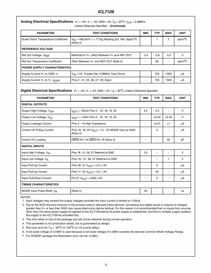
Analog Electrical Specifications V+ = +5V, V- = -5V, GND = 0V, TA = 25oC, fCLK = 3.58MHz,
Unless Otherwise Specified (Continued)
PARAMETER TEST CONDITIONS MIN TYP MAX UNIT
ICL7109
3
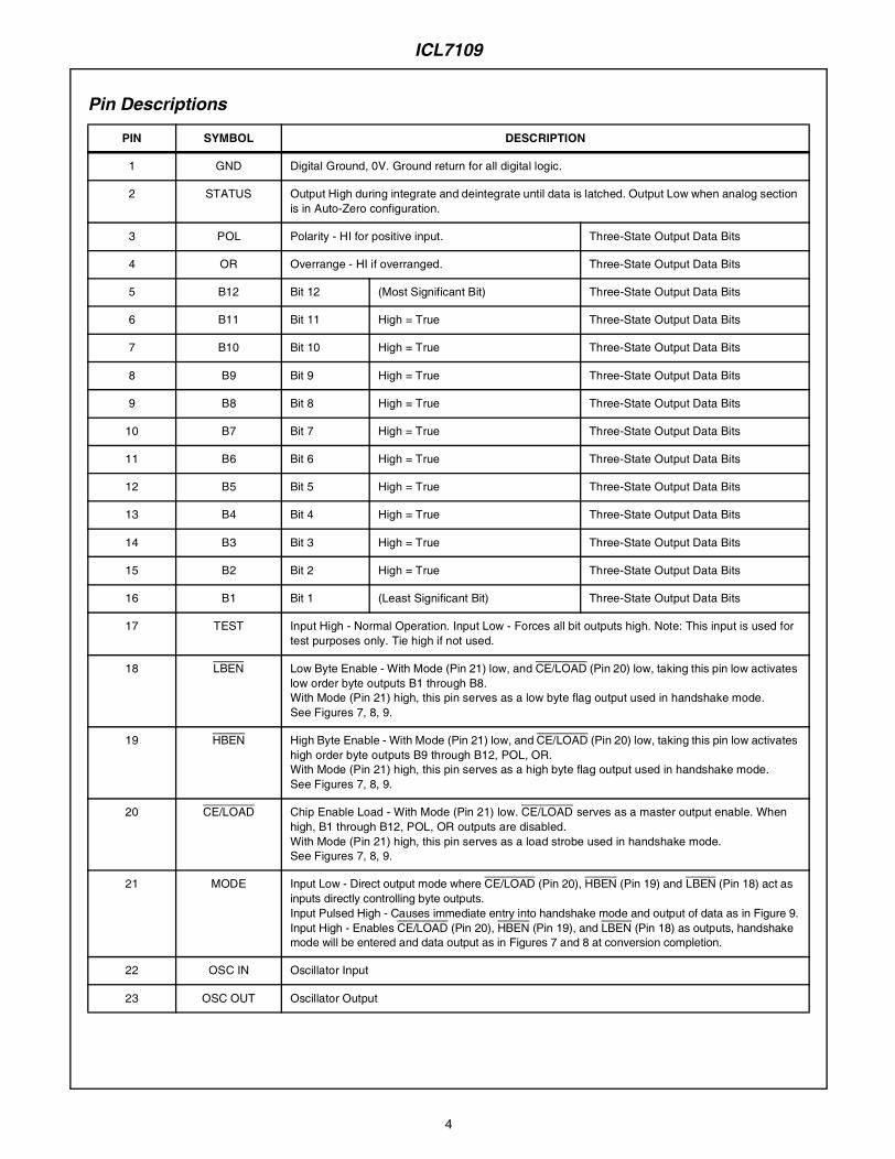
Pin Descriptions
PIN SYMBOL DESCRIPTION
1 GND Digital Ground, 0V. Ground return for all digital logic.
2 STATUS Output High during integrate and deintegrate until data is latched. Output Low when analog section is in Auto-Zero configuration.
3 POL Polarity - HI for positive input. Three-State Output Data Bits
4 OR Overrange - HI if overranged. Three-State Output Data Bits
5 B12 Bit 12 (Most Significant Bit) Three-State Output Data Bits
6 B11 Bit 11 High = True Three-State Output Data Bits
7 B10 Bit 10 High = True Three-State Output Data Bits
8 B9 Bit 9 High = True Three-State Output Data Bits
9 B8 Bit 8 High = True Three-State Output Data Bits
10 B7 Bit 7 High = True Three-State Output Data Bits
11 B6 Bit 6 High = True Three-State Output Data Bits
12 B5 Bit 5 High = True Three-State Output Data Bits
13 B4 Bit 4 High = True Three-State Output Data Bits
14 B3 Bit 3 High = True Three-State Output Data Bits
15 B2 Bit 2 High = True Three-State Output Data Bits
16 B1 Bit 1 (Least Significant Bit) Three-State Output Data Bits
17 TEST Input High - Normal Operation. Input Low - Forces all bit outputs high. Note: This input is used for test purposes only. Tie high if not used.
18 LBEN Low Byte Enable - With Mode (Pin 21) low, and CE/LOAD (Pin 20) low, taking this pin low activates low order byte outputs B1 through B8.With Mode (Pin 21) high, this pin serves as a low byte flag output used in handshake mode. See Figures 7, 8, 9.
19 HBEN High Byte Enable - With Mode (Pin 21) low, and CE/LOAD (Pin 20) low, taking this pin low activates high order byte outputs B9 through B12, POL, OR.With Mode (Pin 21) high, this pin serves as a high byte flag output used in handshake mode.See Figures 7, 8, 9.
20 CE/LOAD Chip Enable Load - With Mode (Pin 21) low. CE/LOAD serves as a master output enable. When high, B1 through B12, POL, OR outputs are disabled.With Mode (Pin 21) high, this pin serves as a load strobe used in handshake mode.See Figures 7, 8, 9.
21 MODE Input Low - Direct output mode where CE/LOAD (Pin 20), HBEN (Pin 19) and LBEN (Pin 18) act as inputs directly controlling byte outputs.Input Pulsed High - Causes immediate entry into handshake mode and output of data as in Figure 9.Input High - Enables CE/LOAD (Pin 20), HBEN (Pin 19), and LBEN (Pin 18) as outputs, handshake mode will be entered and data output as in Figures 7 and 8 at conversion completion.
22 OSC IN Oscillator Input
23 OSC OUT Oscillator Output
ICL7109
4
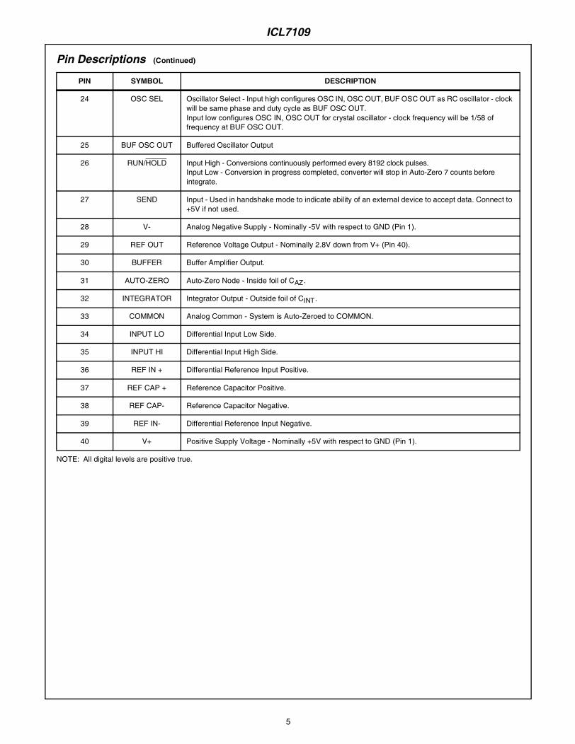
24 OSC SEL Oscillator Select - Input high configures OSC IN, OSC OUT, BUF OSC OUT as RC oscillator - clock will be same phase and duty cycle as BUF OSC OUT.Input low configures OSC IN, OSC OUT for crystal oscillator - clock frequency will be 1/58 of frequency at BUF OSC OUT.
25 BUF OSC OUT Buffered Oscillator Output
26 RUN/HOLD Input High - Conversions continuously performed every 8192 clock pulses.Input Low - Conversion in progress completed, converter will stop in Auto-Zero 7 counts before integrate.
27 SEND Input - Used in handshake mode to indicate ability of an external device to accept data. Connect to +5V if not used.
28 V- Analog Negative Supply - Nominally -5V with respect to GND (Pin 1).
29 REF OUT Reference Voltage Output - Nominally 2.8V down from V+ (Pin 40).
30 BUFFER Buffer Amplifier Output.
31 AUTO-ZERO Auto-Zero Node - Inside foil of CAZ.
32 INTEGRATOR Integrator Output - Outside foil of CINT.
33 COMMON Analog Common - System is Auto-Zeroed to COMMON.
34 INPUT LO Differential Input Low Side.
35 INPUT HI Differential Input High Side.
36 REF IN + Differential Reference Input Positive.
37 REF CAP + Reference Capacitor Positive.
38 REF CAP- Reference Capacitor Negative.
39 REF IN- Differential Reference Input Negative.
40 V+ Positive Supply Voltage - Nominally +5V with respect to GND (Pin 1).
NOTE: All digital levels are positive true.
Pin Descriptions (Continued)
PIN SYMBOL DESCRIPTION
ICL7109
5
6
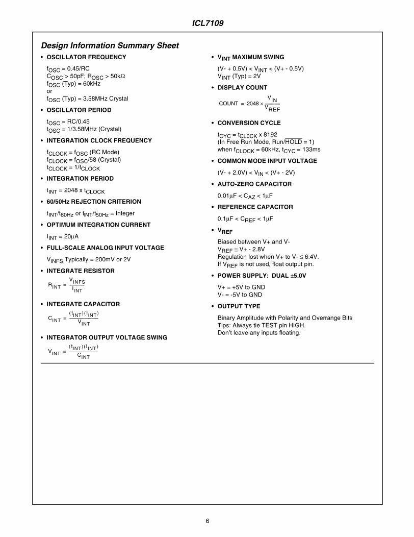
Design Information Summary Sheet• OSCILLATOR FREQUENCY
fOSC = 0.45/RCCOSC > 50pF; ROSC > 50kΩfOSC (Typ) = 60kHzorfOSC (Typ) = 3.58MHz Crystal
• OSCILLATOR PERIOD
tOSC = RC/0.45tOSC = 1/3.58MHz (Crystal)
• INTEGRATION CLOCK FREQUENCY
fCLOCK = fOSC (RC Mode)fCLOCK = fOSC/58 (Crystal)tCLOCK = 1/fCLOCK
• INTEGRATION PERIOD
tINT = 2048 x tCLOCK
• 60/50Hz REJECTION CRITERION
tINT/t60Hz or tlNT/t50Hz = Integer
• OPTIMUM INTEGRATION CURRENT
IINT = 20µA
• FULL-SCALE ANALOG INPUT VOLTAGE
VlNFS Typically = 200mV or 2V
• INTEGRATE RESISTOR
• INTEGRATE CAPACITOR
• INTEGRATOR OUTPUT VOLTAGE SWING
• VINT MAXIMUM SWING
(V- + 0.5V) < VINT < (V+ - 0.5V)VINT (Typ) = 2V
• DISPLAY COUNT
• CONVERSION CYCLE
tCYC = tCL0CK x 8192(In Free Run Mode, Run/HOLD = 1)when fCLOCK = 60kHz, tCYC = 133ms
• COMMON MODE INPUT VOLTAGE
(V- + 2.0V) < VlN < (V+ - 2V)
• AUTO-ZERO CAPACITOR
0.01µF < CAZ < 1µF
• REFERENCE CAPACITOR
0.1µF < CREF < 1µF
• VREF
Biased between V+ and V-VREF ≅ V+ - 2.8VRegulation lost when V+ to V- ≤ 6.4V.If VREF is not used, float output pin.
• POWER SUPPLY: DUAL ±5.0V
V+ = +5V to GNDV- = -5V to GND
• OUTPUT TYPE
Binary Amplitude with Polarity and Overrange BitsTips: Always tie TEST pin HIGH.Don’t leave any inputs floating.
RINT
VINFSIINT
-----------------=
CINT
tINT( ) IINT( )VINT
--------------------------------=
VINT
tINT( ) IINT( )CINT
--------------------------------=
COUNT 2048VIN
VREF-----------------×=
ICL7109
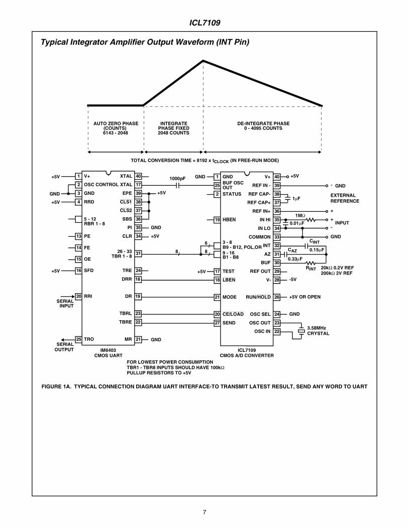
Typical Integrator Amplifier Output Waveform (INT Pin)
AUTO ZERO PHASE(COUNTS) 6143 - 2048
INTEGRATEPHASE FIXED2048 COUNTS
DE-INTEGRATE PHASE0 - 4095 COUNTS
TOTAL CONVERSION TIME = 8192 x tCLOCK (IN FREE-RUN MODE)
FIGURE 1A. TYPICAL CONNECTION DIAGRAM UART INTERFACE-TO TRANSMIT LATEST RESULT, SEND ANY WORD TO UART
18
1
25
2
19
17
21
20
27
GNDBUF OSC
STATUS
HBEN
3 - 8B9 - B12, POL,OR9 - 16
TEST
LBEN
MODE
CE/LOAD
SEND
28
40
39
38
37
36
35
34
33
32
31
30
29
26
24
23
22
V+
REF IN -
REF CAP-
REF CAP+
REF IN+
IN HI
IN LO
COMMON
INT
AZ
BUF
REF OUT
V-
RUN/HOLD
OSC SEL
OSC OUT
OSC IN
GND
GND
+5V
1µF
0.01µF
0.33µF
0.15µFCAZ
CINT
RINT
1MΩ
3.58MHzCRYSTAL
-
+
+INPUT
GND
EXTERNALREFERENCE
-5V
GND
-
20kΩ 0.2V REF200kΩ 2V REF
+5V OR OPEN
OUT
/
/
6
8B1 - B8
1
2
3
4
13
14
15
16
20
25
V+
OSC CONTROL
GND
RRD
5 - 12
PE
FE
OE
SFD
RRI
TRO
18
40
17
39
38
37
36
35
34
31
24
19
23
22
21
XTAL
XTAL
EPE
CLS1
CLS2
SBS
PI
CLR
26 - 33
TRE
DRR
DR
TBRL
TBRE
MR
GND
GND
TBR 1 - 8
+5V
+5V
8/
GND
1000pF
RBR 1 - 8
SERIALOUTPUT
SERIALINPUT
+5V
+5V
+5V
IM6403CMOS UART
ICL7109CMOS A/D CONVERTER
FOR LOWEST POWER CONSUMPTIONTBR1 - TBR8 INPUTS SHOULD HAVE 100kΩPULLUP RESISTORS TO +5V
+5V
ICL7109
7
8
Detailed DescriptionAnalog Section
Figure 2 shows the equivalent circuit of the Analog Sectionfor the ICL7109. When the RUN/HOLD input is left open orconnected to V+, the circuit will perform conversions at arate determined by the clock frequency (8192 clock periodsper cycle). Each measurement cycle is divided into threephases as shown in Figure 3. They are (1) auto-zero (A-Z),(2) signal integrate (INT) and (3) de-integrate (DE).
Auto-Zero Phase
During auto-zero three things happen. First, input high andlow are disconnected from the pins and internally shorted toanalog COMMON. Second, the reference capacitor ischarged to the reference voltage. Third, a feedback loop isclosed around the system to charge the auto-zero capacitorCAZ to compensate for offset voltages in the buffer amplifier,integrator, and comparator. Since the comparator is includedin the loop, the A-Z accuracy is limited only by the noise ofthe system. In any case, the offset referred to the input isless than 10µV.
Signal Integrate Phase
During signal integrate, the auto-zero loop is opened, theinternal short is removed, and the internal input high and loware connected to the external pins. The converter thenintegrates the differential voltage between IN HI and IN LOfor a fixed time. This differential voltage can be within a widecommon mode range of the inputs. At the end of this phase,the polarity of the integrated signal is determined.
FIGURE 1B. TYPICAL CONNECTION DIAGRAM PARALLEL INTERFACE WITH 8048 MICROCOMPUTER
FIGURE 1.
9
25
26
40
39
/5
20
5
6
17
26
19
18
40
1
2
V+
TEST
3 - 8B9 - B12,
9 - 16
STATUS
HBEN
CE/LOAD
28
39
38
37
36
35
34
33
32
31
30
29
26
24
23
21
REF IN -
REF CAP-
REF CAP+
REF IN+
IN HI
IN LO
COMMON
INT
AZ
BUF
REF OUT
V-
RUN/HOLD
OSC SEL
OSC OUT
OSC IN
GND
GND
1µF
0.01µF
0.33µF
0.15µFCAZ
CINT
RINT
1MΩ
3.58MHzCRYSTAL
-
+
+INPUT
GND
EXTERNALREFERENCE
-5V
GND
-
20kΩ 0.2V REF200kΩ 2V REF
+5V OR OPEN
GND
/
/
6
8B1 - B8
1
4
7
8
11
20
XTAL1TO
RESET
EA
WR
ALE
GND
28
30
29
27
10
XTAL2
P12
P11
P10
RD
P13
+5V
8/
27
25
22
MODE
SEND
BUFF OSC OUT
+5V
+5V
SS
INT
2
RUN/HOLD
LBEN
POL,OR
12 - 19DB0 - DB7
31 - 34P14 - P17
35 - 38P20 - P27
/8
21 - 24
OTHERI/O
GND
PSEN
GND
PROG
VDD
VCC
+5V
TL
+5V
+5V
+5V
ICL7109
8748/9048
3 +5V
ICL7109
T
De-Integrate Phase
The final phase is de-integrate, or reference integrate. Inputlow is internally connected to analog COMMON and inputhigh is connected across the previously charged (duringauto-zero) reference capacitor. Circuitry within the chipensures that the capacitor will be connected with the correctpolarity to cause the integrator output to return to zero cross-ing (established in Auto-Zero) with a fixed slope. The timerequired for the output to return to zero is proportional to theinput signal.
Differential Input
The input can accept differential voltages anywhere within thecommon mode range of the input amplifier, or specifically from1V below the positive supply to 1.5V above the negative sup-ply. In this range, the system has a CMRR of 86dB typical.However, care must be exercised to assure the integrator out-put does not saturate. A worst case condition would be a largepositive common mode voltage with a near full-scale negativedifferential input voltage. The negative input signal drives theintegrator positive when most of its swing has been used upby the positive common mode voltage. For these critical appli-cations the integrator output swing can be reduced to lessthan the recommended 4V full scale swing with little loss ofaccuracy. The integrator output can swing to within 0.3V ofeither supply without loss of linearity.
The ICL7109 has, however, been optimized for operationwith analog common near digital ground. With power sup-plies of +5V and -5V, this allows a 4V full scale integratorswing positive or negative thus maximizing the performanceof the analog section.
Differential Reference
The reference voltage can be generated anywhere within thepower supply voltage of the converter. The main source ofcommon mode error is a roll-over voltage caused by thereference capacitor losing or gaining charge to stray capacityon its nodes. If there is a large common mode voltage, the ref-erence capacitor can gain charge (increase voltage) whencalled up to deintegrate a positive signal but lose charge(decrease voltage) when called up to deintegrate a negativeinput signal. This difference in reference for positive ornegative input voltage will give a roll-over error. However, by
selecting the reference capacitor large enough in comparisonto the stray capacitance, this error can be held to less than 0.5count worst case. (See Component Value Selection.)
The roll-over error from these sources is minimized by havingthe reference common mode voltage near or at analogCOMMON.
Component Value Selection
For optimum performance of the analog section, care mustbe taken in the selection of values for the integrator capaci-tor and resistor, auto-zero capacitor, reference voltage, andconversion rate. These values must be chosen to suit theparticular application.
The most important consideration is that the integrator out-put swing (for full-scale input) be as large as possible. Forexample, with ±5V supplies and COMMON connected to
+-+
DE-DE+
CINTCAZ
RINT
BUFFER A-Z INT
-+
A-ZIN HI
COMMON
IN LO
35
33
34
DE- DE+INT
A-Z
37
CREF+
36
REF IN+
CREF
REF IN-
39
A-Z A-Z
38
CREF-
30 31 32
TO ZERO CROSSDETECTORDIGITAL SECTION
A-Z
INTEGRATOR
INT
DE(±)
BUFFER
COMPARATOR
REF OUT
6.2V
29 28 40
10µA
V- V+
AZ
INT
DE+
DE-
FROM CONTROLLOGICDIGITAL SECTION
-+
FIGURE 2. ANALOG SECTION OF ICL7109
eflon™ is a trademark of DuPont Corporation
ICL7109
9
10
GND, the normal integrator output swing at full scale is ±4V.Since the integrator output can go to 0.3V from either supplywithout significantly affecting linearity, a 4V integrator outputswing allows 0.7V for variations in output swing due to com-ponent value and oscillator tolerances. With ±5V suppliesand a common mode range of ±1V required, the componentvalues should be selected to provide ±3V integrator outputswing. Noise and roll-over will be slightly worse than in the±4V case. For larger common mode voltage ranges, the inte-grator output swing must be reduced further. This willincrease both noise and roll-over errors. To improve the per-formance, supplies of ±6V may be used.
Integrating Resistor
Both the buffer amplifier and the integrator have a class A outputstage with 100µA of quiescent current. They supply 20µA of drivecurrent with negligible nonlinearity. The integrating resistorshould be large enough to remain in this very linear region overthe input voltage range, but small enough that undue leakagerequirements are not placed on the PC board. For 409.6mV full-scale, 200kΩ is near optimum and similarly a 20kΩ for a409.6mV scale. For other values of full scale voltage, RINTshould be chosen by the relation :
Integrating Capacitor
The integrating capacitor CINT should be selected to give themaximum voltage swing that ensures tolerance build-up willnot saturate the integrator swing (approximately. 0.3V fromeither supply). For the ICL7109 with ±5V supplies and analogcommon connected to GND, a ±3.5V to ±4V integrator outputswing is nominal. For 71/2 conversions per second (61.72kHzclock frequency) as provided by the crystal oscillator, nominalvalues for CINT and CAZ are 0.15µF and 0.33µF, respec-tively. If different clock frequencies are used, these valuesshould be changed to maintain the integrator output swing. Ingeneral, the value CINT is given by:
.
An additional requirement of the integrating capacitor is thatit have low dielectric absorption to prevent roll-over errors.While other types of capacitors are adequate for this applica-tion, polypropylene capacitors give undetectable errors atThe integrating capacitor should have a low dielectricabsorption to prevent roll-over errors. While other types maybe adequate for this application, polypropylene capacitorsgive undetectable errors at reasonable cost up to 85oC.Teflon™ capacitors are recommended for the military tem-perature range. While their dielectric absorption characteris-tics vary somewhat from unit to unit, selected devices shouldgive less than 0.5 count of error due to dielectric absorption.
Auto-Zero Capacitor
The size of the auto-zero capacitor has some influence onthe noise of the system: a smaller physical size and a largercapacitance value lower the overall system noise. However,CAZ cannot be increased without limits since it, in parallel
with the integrating capacitor forms an R-C time constantthat determines the speed of recovery from overloads andthe error that exists at the end of an auto-zero cycle. For409.6mV full scale where noise is very important and theintegrating resistor small, a value of CAZ twice CINT is opti-mum. Similarly for 4.096V full scale where recovery is moreimportant than noise, a value of CAZ equal to half of CINT isrecommended.
For optimal rejection of stray pickup, the outer foil of CAZshould be connected to the R-C summing junction and theinner foil to pin 31. Similarly the outer foil of CINT should beconnected to pin 32 and the inner foil to the R-C summingjunction. Teflon, or equivalent, capacitors are recommendedabove 85oC for their low leakage characteristics.
Reference Capacitor
A 1µF capacitor gives good results in most applications.However, where a large reference common mode voltageexists (i.e., the reference low is not at analog common) anda 409.6mV scale is used, a large value is required to preventroll-over error. Generally 10µF will hold the roll-over error to0.5 count in this instance. Again, Teflon, or equivalentcapacitors should be used for temperatures above 85oC fortheir low leakage characteristics.
RINTfull scale voltage
20µA--------------------------------------------
·.=
CINT2048 clock period×( ) 20µA( )
integrator output voltage swing---------------------------------------------------------------------------------=
ICL7109
Reference Voltage
The analog input required to generate a full scale output of4096 counts is VIN = 2VREF. For normalized scale, a refer-ence of 2.048V should be used for a 4.096V full scale, and204.8mV should be used for a 0.4096V full scale. However,in many applications where the A/D is sensing the output ofa transducer, there will exist a scale factor other than unitybetween the absolute output voltage to be measured and adesired digital output. For instance, in a weighing system,the designer might like to have a full scale reading when thevoltage from the transducer is 0.682V. Instead of driving theinput down to 409.6mV, the input voltage should be mea-sured directly and a reference voltage of 0.341V should beused. Suitable values for integrating resistor and capacitorare 33kΩ and 0.15µF. This avoids a divider on the input.Another advantage of this system occurs when a zero read-ing is desired for non-zero input. Temperature and weightmeasurements with an offset or tare are examples. The off-set may be introduced by connecting the voltage output ofthe transducer between common and analog high, and theoffset voltage between common and analog low, observingpolarities carefully. However, in processor-based systemsusing the ICL7109, it may be more efficient to perform thistype of scaling or tare subtraction digitally using software.
Reference Sources
The stability of the reference voltage is a major factor in theoverall absolute accuracy of the converter. The resolution ofthe ICL7109 at 12 bits is one part in 4096, or 244ppm. Thusif the reference has a temperature coefficient of 80ppm/oC(onboard reference) a temperature difference of 3oC willintroduce a one-bit absolute error.
For this reason, it is recommended that an external high-quality reference be used where the ambient temperature isnot controlled or where high-accuracy absolute measure-
ments are being made.
The ICL7109 provides a REFerence OUTput (Pin 29) whichmay be used with a resistive divider to generate a suitablereference voltage. This output will sink up to about 20mAwithout significant variation in output voltage, and is providedwith a pullup bias device which sources about 10µA. Theoutput voltage is nominally 2.8V below V+, and has a tem-perature coefficient of ±80ppm/oC (Typ). When using theonboard reference, REF OUT (Pin 29) should be connectedto REF- (Pin 39), and REF+ should be connected to thewiper of a precision potentiometer between REF OUT andV+. The circuit for a 204.8mV reference is shown in the testcircuit. For a 2.048mV reference, the fixed resistor should beremoved, and a 25kΩ precision potentiometer between REFOUT and V+ should be used.
Note that if Pins 29 and 39 are tied together and Pins 39 and40 accidentally shorted (e.g., during testing), the referencesupply will sink enough current to destroy the device. This canbe avoided by placing a 1kΩ resistor in series with Pin 39.
Detailed Description
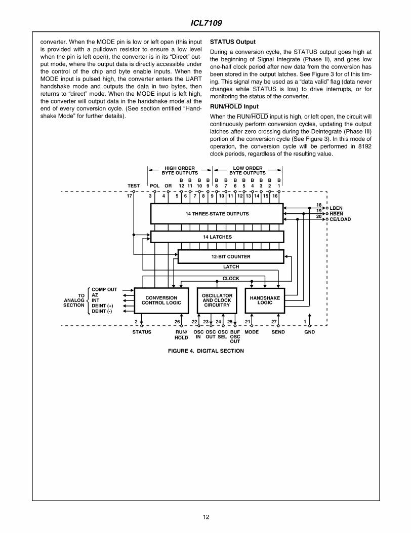
Digital Section
The digital section includes the clock oscillator and scalingcircuit, a 12-bit binary counter with output latches and TTL-compatible three-state output drivers, polarity, over-rangeand control logic, and UART handshake logic, as shown inFigure 4.
Throughout this description, logic levels will be referred to as“low” or “high”. The actual logic levels are defined in the Elec-trical Specifications Table. For minimum power consumption,all inputs should swing from GND (low) to V+ (high). Inputsdriven from TTL gates should have 3-5kΩ pullup resistors
MODE Input The MODE input is used to control the output mode of the
AZ PHASE I INT PHASE II DEINT PHASE III AZ
INTERNAL CLOCK
INTERNAL LATCH
STATUS OUTPUT
INTEGRATOROUTPUT
POLARITYDETECTED
ZERO CROSSINGOCCURS
ZERO CROSSINGDETECTED
4096 COUNTSMAX
FIXED 2048COUNTS
2048 COUNTSMINIMUM
NUMBER OF COUNTS TO ZERO CROSSINGPROPORTIONAL TO VIN
AFTER ZERO CROSSINGANALOG SECTION WILLBE IN AUTOZEROCONFIGURATION
FIGURE 3. CONVERSION TIMING (RUN/HOLD PIN HIGH)
ICL7109
11
12
converter. When the MODE pin is low or left open (this inputis provided with a pulldown resistor to ensure a low levelwhen the pin is left open), the converter is in its “Direct” out-put mode, where the output data is directly accessible underthe control of the chip and byte enable inputs. When theMODE input is pulsed high, the converter enters the UARThandshake mode and outputs the data in two bytes, thenreturns to “direct” mode. When the MODE input is left high,the converter will output data in the handshake mode at theend of every conversion cycle. (See section entitled “Hand-shake Mode” for further details).
STATUS Output
During a conversion cycle, the STATUS output goes high atthe beginning of Signal Integrate (Phase II), and goes lowone-half clock period after new data from the conversion hasbeen stored in the output latches. See Figure 3 for of this tim-ing. This signal may be used as a “data valid” flag (data neverchanges while STATUS is low) to drive interrupts, or formonitoring the status of the converter.
RUN/HOLD Input
When the RUN/HOLD input is high, or left open, the circuit willcontinuously perform conversion cycles, updating the outputlatches after zero crossing during the Deintegrate (Phase III)portion of the conversion cycle (See Figure 3). In this mode ofoperation, the conversion cycle will be performed in 8192clock periods, regardless of the resulting value.
FIGURE 4. DIGITAL SECTION
TEST
LATCH
CLOCK
POL OR 12 11 10 9 8 7 6 5 4 3 2 1
17 3 4 5 6 7 8 9 10 11 12 13 14 15 16
2 26 22 23 24 25 21 27
STATUS RUN/ OSC OSC OSC BUF MODE SENDHOLD IN OUT SEL OSC
OUT
LOW ORDERBYTE OUTPUTS
B B B B B B B B B B B B
GND
1
181920
LBENHBENCE/LOAD
TOANALOGSECTION
COMP OUTAZINTDEINT (+)DEINT (-)
CONVERSIONCONTROL LOGIC
OSCILLATORAND CLOCKCIRCUITRY
HIGH ORDERBYTE OUTPUTS
12-BIT COUNTER
14 LATCHES
14 THREE-STATE OUTPUTS
HANDSHAKELOGIC
ICL7109
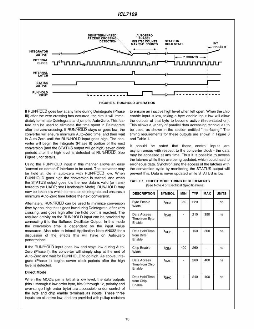
If RUN/HOLD goes low at any time during Deintegrate (PhaseIII) after the zero crossing has occurred, the circuit will imme-diately terminate Deintegrate and jump to Auto-Zero. This fea-ture can be used to eliminate the time spent in Deintegrateafter the zero-crossing. If RUN/HOLD stays or goes low, theconverter will ensure minimum Auto-Zero time, and then waitin Auto-Zero until the RUN/HOLD input goes high. The con-verter will begin the Integrate (Phase II) portion of the nextconversion (and the STATUS output will go high) seven clockperiods after the high level is detected at RUN/HOLD. SeeFigure 5 for details.
Using the RUN/HOLD input in this manner allows an easy“convert on demand” interface to be used. The converter maybe held at idle in auto-zero with RUN/HOLD low. WhenRUN/HOLD goes high the conversion is started, and whenthe STATUS output goes low the new data is valid (or trans-ferred to the UART; see Handshake Mode). RUN/HOLD maynow be taken low which terminates deintegrate and ensures aminimum Auto-Zero time before the next conversion.
Alternately, RUN/HOLD can be used to minimize conversiontime by ensuring that it goes low during Deintegrate, after zerocrossing, and goes high after the hold point is reached. Therequired activity on the RUN/HOLD input can be provided byconnecting it to the Buffered Oscillator Output. In this modethe conversion time is dependent on the input valuemeasured. Also refer to Intersil Application Note AN032 for adiscussion of the effects this will have on Auto-Zeroperformance.
If the RUN/HOLD input goes low and stays low during Auto-Zero (Phase I), the converter will simply stop at the end ofAuto-Zero and wait for RUN/HOLD to go high. As above, Inte-grate (Phase II) begins seven clock periods after the highlevel is detected.
Direct Mode
When the MODE pin is left at a low level, the data outputs(bits 1 through 8 low order byte, bits 9 through 12, polarity andover-range high order byte) are accessible under control ofthe byte and chip enable terminals as inputs. These threeinputs are all active low, and are provided with pullup resistors
to ensure an inactive high level when left open. When the chipenable input is low, taking a byte enable input low will allowthe outputs of that byte to become active (three-stated on).This allows a variety of parallel data accessing techniques tobe used, as shown in the section entitled “Interfacing.” Thetiming requirements for these outputs are shown in Figure 6and Table 1.
It should be noted that these control inputs areasynchronous with respect to the converter clock - the datamay be accessed at any time. Thus it is possible to accessthe latches while they are being updated, which could lead toerroneous data. Synchronizing the access of the latches withthe conversion cycle by monitoring the STATUS output willprevent this. Data is never updated while STATUS is low.
FIGURE 5. RUN/HOLD OPERATION
INTPHASE II
STATIC INHOLD STATE
7 COUNTS
AUTOZEROPHASE I
MIN 1790 COUNTSMAX 2041 COUNTS
DEINT TERMINATEDAT ZERO CROSSING
DETECTION
INTERNALCLOCK
INTERNALLATCH
STATUSOUTPUT
RUN/HOLDINPUT
INTEGRATOROUTPUT
TABLE 1. DIRECT MODE TIMING REQUIREMENTS(See Note 4 of Electrical Specifications)
DESCRIPTION SYMBOL MIN TYP MAX UNITS
Byte Enable Width
tBEA 350 220 - ns
Data Access Time from Byte Enable
tDAB - 210 350 ns
Data Hold Time from ByteEnable
tDHB - 150 300 ns
Chip Enable Width
tCEA 400 260 - ns
Data Access Time from Chip Enable
tDAC - 260 400 ns
Data Hold Time from ChipEnable
tDHC - 240 400 ns
ICL7109
13
14
Handshake Mode
The handshake output mode is provided as an alternativemeans of interfacing the ICL7109 to digital systems where theA/D converter becomes active in controlling the flow of datainstead of passively responding to chip and byte enableinputs. This mode is specifically designed to allow a directinterface between the ICL7109 and industry-standard UARTs(such as the Intersil IM6402/3) with no external logic required.When triggered into the handshake mode, the ICL7109 pro-vides all the control and flag signals necessary to sequentiallytransfer two bytes of data into the UART and initiate theirtransmission in serial form. This greatly eases the task andreduces the cost of designing remote data acquisition stationsusing serial data transmission.
Entry into the handshake mode is controlled by the MODE pin.When the MODE terminal is held high, the ICL7109 will enterthe handshake mode after new data has been stored in the out-put latches at the end of a conversion (See Figures 7 and 8).The MODE terminal may also be used to trigger entry into thehandshake mode on demand. At any time during the conver-sion cycle, the low to high transition of a short pulse at theMODE input will cause immediate entry into the handshakemode. If this pulse occurs while new data is being stored, theentry into handshake mode is delayed until the data is stable.While the converter is in the handshake mode, the MODE inputis ignored, and although conversions will still be performed,data updating will be inhibited (See Figure 9) until the convertercompletes the output cycle and clears the handshake mode.
When the converter enters the handshake mode, or when theMODE input is high, the chip and byte enable terminalsbecome TTL-compatible outputs which provide the control
signals for the output cycle (See Figures 7, 8, and 9).
In handshake mode, the SEND input is used by the converteras an indication of the ability of the receiving device (such as aUART) to accept data.
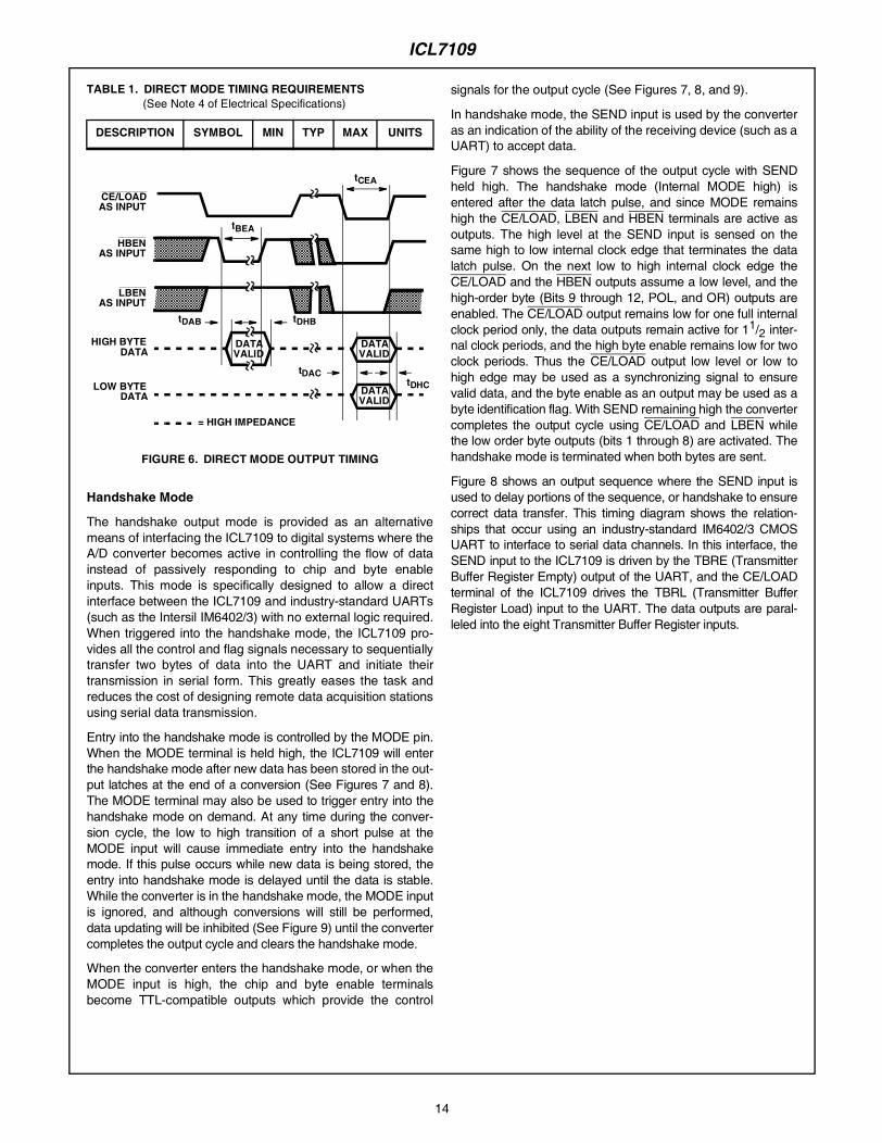
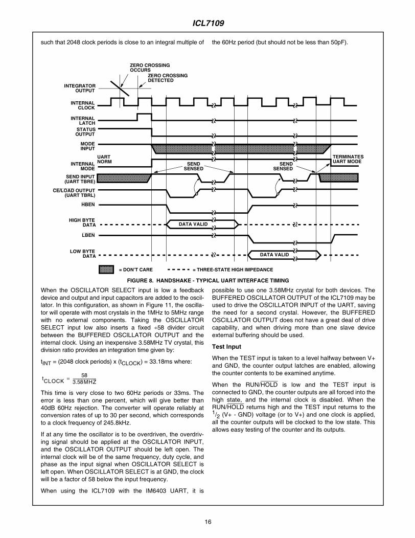
Figure 7 shows the sequence of the output cycle with SENDheld high. The handshake mode (Internal MODE high) isentered after the data latch pulse, and since MODE remainshigh the CE/LOAD, LBEN and HBEN terminals are active asoutputs. The high level at the SEND input is sensed on thesame high to low internal clock edge that terminates the datalatch pulse. On the next low to high internal clock edge theCE/LOAD and the HBEN outputs assume a low level, and thehigh-order byte (Bits 9 through 12, POL, and OR) outputs areenabled. The CE/LOAD output remains low for one full internalclock period only, the data outputs remain active for 11/2 inter-nal clock periods, and the high byte enable remains low for twoclock periods. Thus the CE/LOAD output low level or low tohigh edge may be used as a synchronizing signal to ensurevalid data, and the byte enable as an output may be used as abyte identification flag. With SEND remaining high the convertercompletes the output cycle using CE/LOAD and LBEN whilethe low order byte outputs (bits 1 through 8) are activated. Thehandshake mode is terminated when both bytes are sent.
Figure 8 shows an output sequence where the SEND input isused to delay portions of the sequence, or handshake to ensurecorrect data transfer. This timing diagram shows the relation-ships that occur using an industry-standard IM6402/3 CMOSUART to interface to serial data channels. In this interface, theSEND input to the ICL7109 is driven by the TBRE (TransmitterBuffer Register Empty) output of the UART, and the CE/LOADterminal of the ICL7109 drives the TBRL (Transmitter BufferRegister Load) input to the UART. The data outputs are paral-leled into the eight Transmitter Buffer Register inputs.
FIGURE 6. DIRECT MODE OUTPUT TIMING
TABLE 1. DIRECT MODE TIMING REQUIREMENTS(See Note 4 of Electrical Specifications)
DESCRIPTION SYMBOL MIN TYP MAX UNITS
DATAVALID
DATAVALID
DATAVALID
tCEA
tBEA
tDAB tDHB
tDACtDHC
CE/LOADAS INPUT
HBENAS INPUT
LBENAS INPUT
HIGH BYTEDATA
LOW BYTEDATA
= HIGH IMPEDANCE
ICL7109
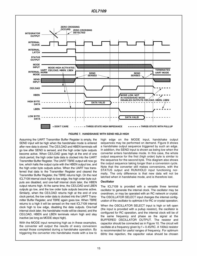
Assuming the UART Transmitter Buffer Register is empty, theSEND input will be high when the handshake mode is enteredafter new data is stored. The CE/LOAD and HBEN terminals willgo low after SEND is sensed, and the high order byte outputsbecome active. When CE/LOAD goes high at the end of oneclock period, the high order byte data is clocked into the UARTTransmitter Buffer Register. The UART TBRE output will now golow, which halts the output cycle with the HBEN output low, andthe high order byte outputs active. When the UART has trans-ferred that data to the Transmitter Register and cleared theTransmitter Buffer Register, the TBRE returns high. On the nextICL7109 internal clock high to low edge, the high order byte out-puts are disabled, and one-half internal clock later, the HBENoutput returns high. At the same time, the CE/LOAD and LBENoutputs go low, and the low order byte outputs become active.Similarly, when the CE/LOAD returns high at the end of oneclock period, the low order data is clocked into the UART Trans-mitter Buffer Register, and TBRE again goes low. When TBREreturns to a high it will be sensed on the next ICL7109 internalclock high to low edge, disabling the data outputs. One-halfinternal clock later, the handshake mode will be cleared, and theCE/LOAD, HBEN and LBEN terminals return high and stayinactive (as long as MODE stays high).
With the MODE input remaining high as in these examples,the converter will output the results of every conversionexcept those completed during a handshake operation. Bytriggering the converter into handshake mode with a low to
high edge on the MODE input, handshake outputsequences may be performed on demand. Figure 9 showsa handshake output sequence triggered by such an edge.In addition, the SEND input is shown as being low when theconverter enters handshake mode. In this case, the wholeoutput sequence for the first (high order) byte is similar tothe sequence for the second byte. This diagram also showsthe output sequence taking longer than a conversion cycle.Note that the converter still makes conversions, with theSTATUS output and RUN/HOLD input functioning nor-mally. The only difference is that new data will not belatched when in handshake mode, and is therefore lost.
Oscillator
The ICL7109 is provided with a versatile three terminaloscillator to generate the internal clock. The oscillator may beoverdriven, or may be operated with an RC network or crystal.The OSCILLATOR SELECT input changes the internal config-uration of the oscillator to optimize it for RC or crystal operation.
When the OSCILLATOR SELECT input is high or left open(the input is provided with a pullup resistor), the oscillator isconfigured for RC operation, and the internal clock will be ofthe same frequency and phase as the signal at theBUFFERED OSCILLATOR OUTPUT. The resistor andcapacitor should be connected as in Figure 10. The circuit willoscillate at a frequency given by f = 0.45/RC. A 100kΩ resistoris recommended for useful ranges of frequency. For optimum60Hz line rejection, the capacitor value should be chosen
INTEGRATOROUTPUT
INTERNALCLOCK
INTERNALLATCH
STATUSOUTPUT
MODE
INTERNALMODE
SENDINPUT
CE/LOAD
HBEN
HIGH BYTEDATA
LBEN
LOW BYTEDATA
= DON’T CARE
INPUT
ZERO CROSSINGOCCURS ZERO CROSSING
DETECTED
MODE HIGH ACTIVATESCE/LOAD, HBEN, LBENUART
NORM SENDSENSED
SENDSENSED
TERMINATESUART MODE
= THREE-STATE HIGH IMPEDANCE = THREE-STATE WITH PULLUP
MODE LOW, NOTIN HANDSHAKE MODEDISABLES OUTPUTS CE/LOAD, HBEN, LBEN
DATA VALID
DATA VALID
FIGURE 7. HANDSHAKE WITH SEND HELD HIGH
ICL7109
15
16
such that 2048 clock periods is close to an integral multiple of the 60Hz period (but should not be less than 50pF).
When the OSCILLATOR SELECT input is low a feedbackdevice and output and input capacitors are added to the oscil-lator. In this configuration, as shown in Figure 11, the oscilla-tor will operate with most crystals in the 1MHz to 5MHz rangewith no external components. Taking the OSCILLATORSELECT input low also inserts a fixed ÷58 divider circuitbetween the BUFFERED OSCILLATOR OUTPUT and theinternal clock. Using an inexpensive 3.58MHz TV crystal, thisdivision ratio provides an integration time given by:
tINT = (2048 clock periods) x (tCLOCK) = 33.18ms where:
This time is very close to two 60Hz periods or 33ms. Theerror is less than one percent, which will give better than40dB 60Hz rejection. The converter will operate reliably atconversion rates of up to 30 per second, which correspondsto a clock frequency of 245.8kHz.
If at any time the oscillator is to be overdriven, the overdriv-ing signal should be applied at the OSCILLATOR INPUT,and the OSCILLATOR OUTPUT should be left open. Theinternal clock will be of the same frequency, duty cycle, andphase as the input signal when OSCILLATOR SELECT isleft open. When OSCILLATOR SELECT is at GND, the clockwill be a factor of 58 below the input frequency.
When using the ICL7109 with the IM6403 UART, it is
possible to use one 3.58MHz crystal for both devices. TheBUFFERED OSCILLATOR OUTPUT of the ICL7109 may beused to drive the OSCILLATOR INPUT of the UART, savingthe need for a second crystal. However, the BUFFEREDOSCILLATOR OUTPUT does not have a great deal of drivecapability, and when driving more than one slave deviceexternal buffering should be used.
Test Input
When the TEST input is taken to a level halfway between V+and GND, the counter output latches are enabled, allowingthe counter contents to be examined anytime.
When the RUN/HOLD is low and the TEST input isconnected to GND, the counter outputs are all forced into thehigh state, and the internal clock is disabled. When theRUN/HOLD returns high and the TEST input returns to the1/2 (V+ - GND) voltage (or to V+) and one clock is applied,all the counter outputs will be clocked to the low state. Thisallows easy testing of the counter and its outputs.
ZERO CROSSINGOCCURS
ZERO CROSSINGDETECTED
INTEGRATOROUTPUT
INTERNALCLOCK
INTERNALLATCH
STATUSOUTPUT
MODEINPUT
INTERNALMODE
UARTNORM
SEND INPUT(UART TBRE)
CE/LOAD OUTPUT(UART TBRL)
HBEN
HIGH BYTEDATA
LBEN
LOW BYTEDATA
= DON’T CARE = THREE-STATE HIGH IMPEDANCE
SENDSENSED
SENDSENSED
TERMINATESUART MODE
DATA VALID
DATA VALID
FIGURE 8. HANDSHAKE - TYPICAL UART INTERFACE TIMING
tCLOCK58
3.58MHZ--------------------------=
ICL7109
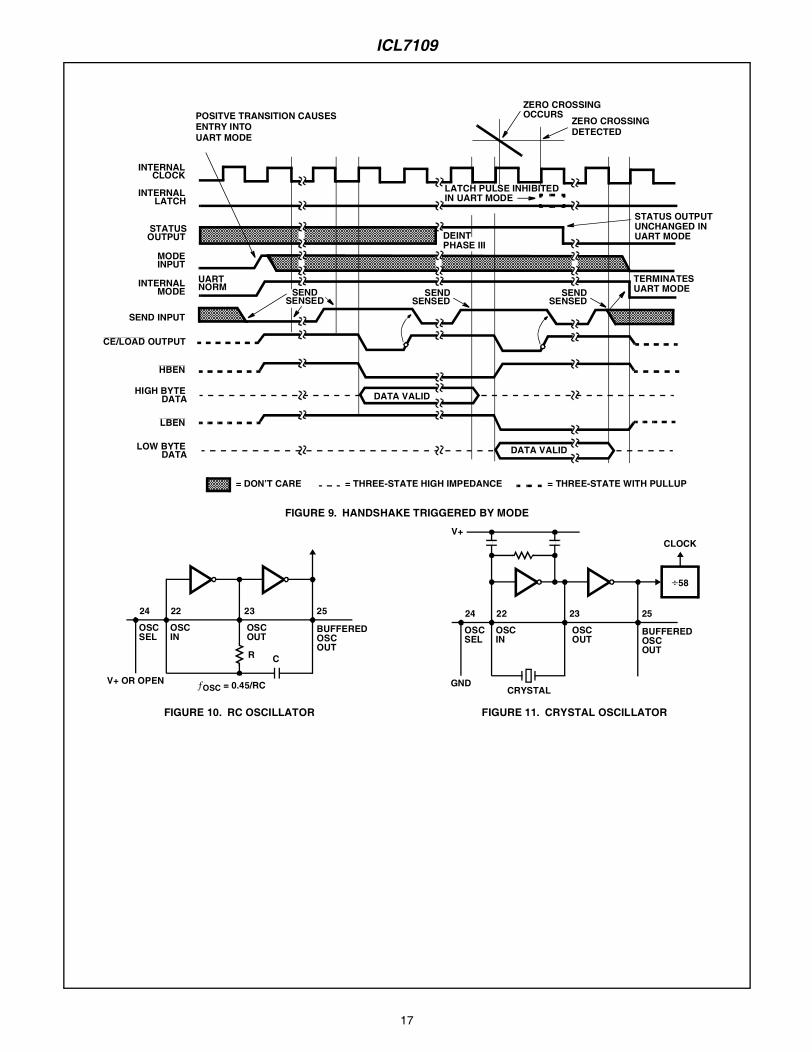
FIGURE 10. RC OSCILLATOR FIGURE 11. CRYSTAL OSCILLATOR
ZERO CROSSINGOCCURS
ZERO CROSSINGDETECTED
INTERNALCLOCK
INTERNALLATCH
STATUSOUTPUT
MODEINPUT
INTERNALMODE
UARTNORM
SEND INPUT
CE/LOAD OUTPUT
HBEN
HIGH BYTEDATA
LBEN
LOW BYTEDATA
= DON’T CARE = THREE-STATE HIGH IMPEDANCE
SENDSENSED
SENDSENSED
TERMINATESUART MODE
DATA VALID
DATA VALID
= THREE-STATE WITH PULLUP
SENDSENSED
LATCH PULSE INHIBITEDIN UART MODE
DEINTPHASE III
STATUS OUTPUTUNCHANGED INUART MODE
POSITVE TRANSITION CAUSESENTRY INTOUART MODE
FIGURE 9. HANDSHAKE TRIGGERED BY MODE
25
OSCSEL
BUFFEREDOSCOUT
V+ OR OPEN
R C
ƒOSC = 0.45/RC
OSCIN
OSCOUT
232224 25
OSCSEL
BUFFEREDOSCOUT
GNDCRYSTAL
OSCIN
OSCOUT
232224
÷58
V+CLOCK
ICL7109
17
18
FIGURE 12. DIRECT MODE CHIP AND BYTE ENABLE COMBINATIONS
FIGURE 13. THREE-STATE SEVERAL ICL7109’S TO A SMALL BUS
GND
MODE
LBEN
B9 - B12POL, OR
B1 - B8
RUN/HOLD
HBENCONVERT
ANALOGIN
CONTROL
6
8
ICL7109
GND
MODE
LBEN
B1 - B12POL, OR
RUN/HOLD
HBENCONVERT
ANALOGIN
14
ICL7109
GND
MODE
LBEN
B9 - B12POL, OR
B1 - B8
RUN/HOLD
HBENCONVERT
ANALOGIN
BYTE FLAGS
6
8
ICL7109
CE/LOAD CE/LOADCE/LOAD
CHIP SELECT 1
GND ORCHIP SELECT 2
CHIP SELECT
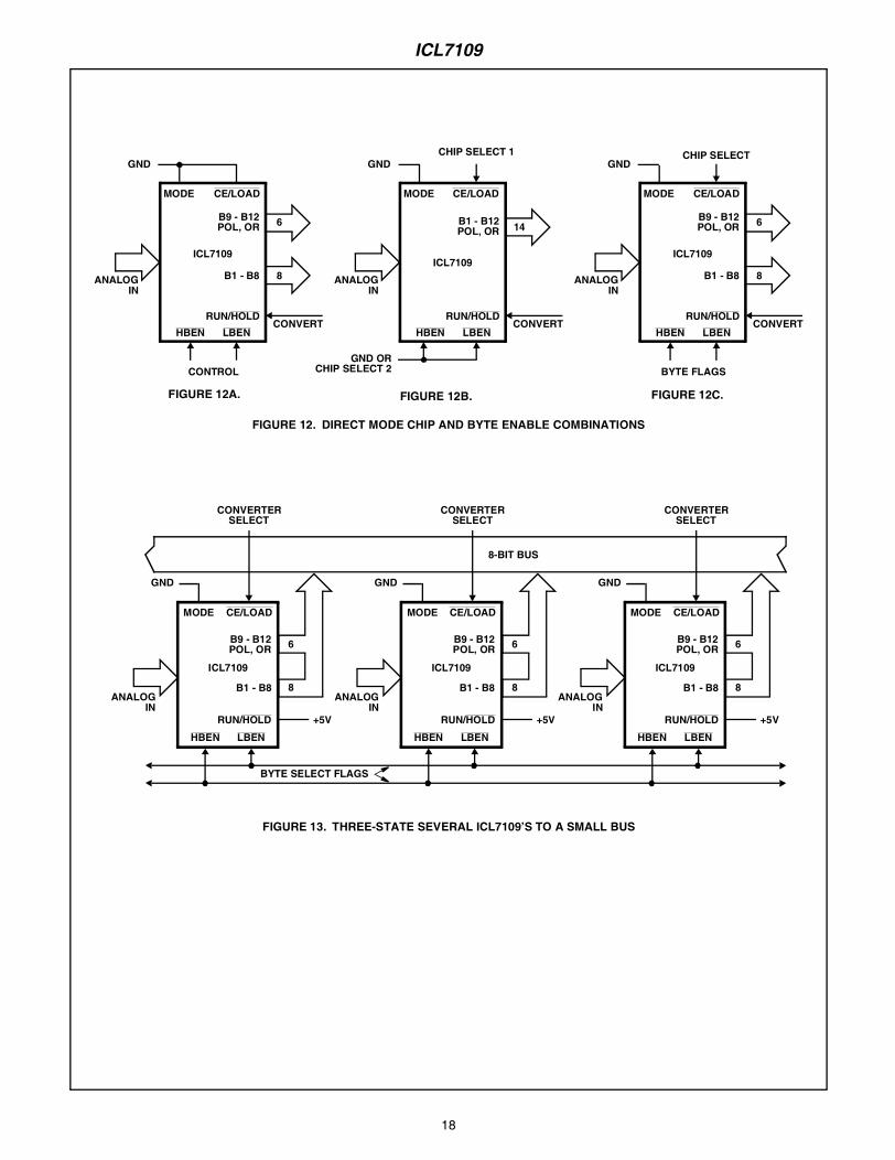
FIGURE 12A. FIGURE 12B. FIGURE 12C.
GND
CE/LOAD
LBEN
B9 - B12POL, OR
B1 - B8
HBEN
ANALOGIN
6
8
MODE
RUN/HOLD +5V
CONVERTERSELECT
8-BIT BUS
GND
CE/LOAD
LBEN
B9 - B12POL, OR
B1 - B8
HBEN
ANALOGIN
6
8
MODE
RUN/HOLD +5V
CONVERTERSELECT
GND
CE/LOAD
LBEN
B9 - B12POL, OR
B1 - B8
HBEN
ANALOGIN
6
8
MODE
RUN/HOLD +5V
CONVERTERSELECT
ICL7109 ICL7109 ICL7109
BYTE SELECT FLAGS
ICL7109
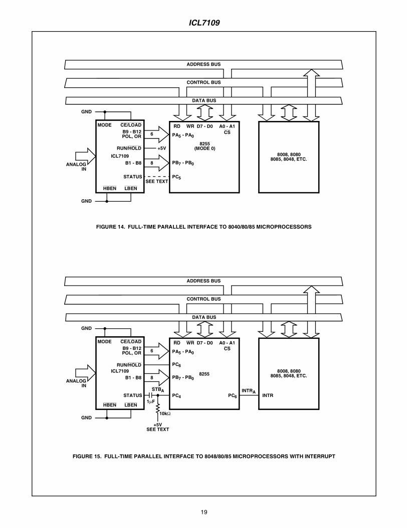
FIGURE 14. FULL-TIME PARALLEL INTERFACE TO 8040/80/85 MICROPROCESSORS
FIGURE 15. FULL-TIME PARALLEL INTERFACE TO 8048/80/85 MICROPROCESSORS WITH INTERRUPT
GND
MODE
LBEN
B9 - B12POL, OR
B1 - B8
STATUS
HBEN
SEE TEXT
ANALOGIN
6
8ICL7109
CE/LOAD
RUN/HOLD +5V
GND
ADDRESS BUS
CONTROL BUS
RD WR
PA5 - PA0
PB7 - PB0
PC5
D7 - D0 A0 - A1CS
8255(MODE 0)
8008, 80808085, 8048, ETC.
DATA BUS
GND
MODE
LBEN
B9 - B12POL, OR
B1 - B8
STATUS
HBEN
+5V
ANALOGIN
6
8ICL7109
CE/LOAD
RUN/HOLD
GND
ADDRESS BUS
CONTROL BUS
RD WR
PA5 - PA0
PB7 - PB0
PC4
D7 - D0 A0 - A1CS
82558008, 8080
8085, 8048, ETC.
PC6
SEE TEXT
STBA
1µF
10kΩ
PC6INTRA
INTR
DATA BUS
ICL7109
19
20
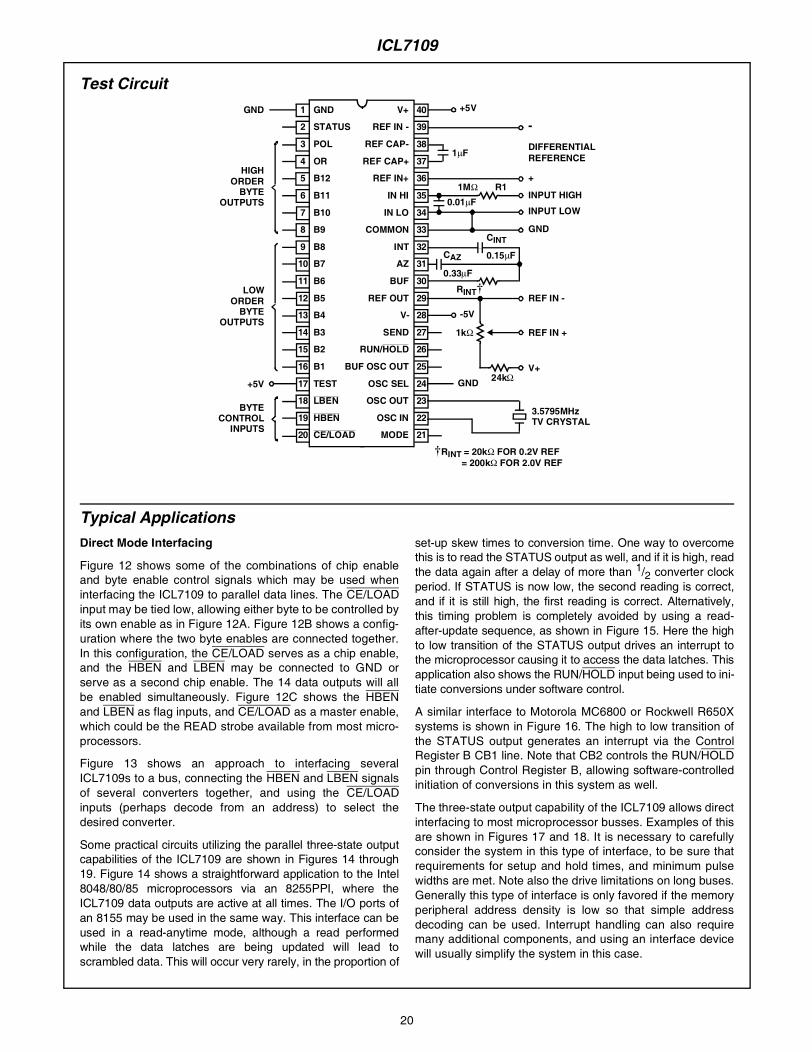
Test Circuit
Typical Applications
Direct Mode Interfacing
Figure 12 shows some of the combinations of chip enableand byte enable control signals which may be used wheninterfacing the ICL7109 to parallel data lines. The CE/LOADinput may be tied low, allowing either byte to be controlled byits own enable as in Figure 12A. Figure 12B shows a config-uration where the two byte enables are connected together.In this configuration, the CE/LOAD serves as a chip enable,and the HBEN and LBEN may be connected to GND orserve as a second chip enable. The 14 data outputs will allbe enabled simultaneously. Figure 12C shows the HBENand LBEN as flag inputs, and CE/LOAD as a master enable,which could be the READ strobe available from most micro-processors.
Figure 13 shows an approach to interfacing severalICL7109s to a bus, connecting the HBEN and LBEN signalsof several converters together, and using the CE/LOADinputs (perhaps decode from an address) to select thedesired converter.
Some practical circuits utilizing the parallel three-state outputcapabilities of the ICL7109 are shown in Figures 14 through19. Figure 14 shows a straightforward application to the Intel8048/80/85 microprocessors via an 8255PPI, where theICL7109 data outputs are active at all times. The I/O ports ofan 8155 may be used in the same way. This interface can beused in a read-anytime mode, although a read performedwhile the data latches are being updated will lead toscrambled data. This will occur very rarely, in the proportion of
set-up skew times to conversion time. One way to overcomethis is to read the STATUS output as well, and if it is high, readthe data again after a delay of more than 1/2 converter clockperiod. If STATUS is now low, the second reading is correct,and if it is still high, the first reading is correct. Alternatively,this timing problem is completely avoided by using a read-after-update sequence, as shown in Figure 15. Here the highto low transition of the STATUS output drives an interrupt tothe microprocessor causing it to access the data latches. Thisapplication also shows the RUN/HOLD input being used to ini-tiate conversions under software control.
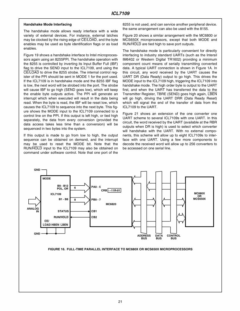
A similar interface to Motorola MC6800 or Rockwell R650Xsystems is shown in Figure 16. The high to low transition ofthe STATUS output generates an interrupt via the ControlRegister B CB1 line. Note that CB2 controls the RUN/HOLDpin through Control Register B, allowing software-controlledinitiation of conversions in this system as well.
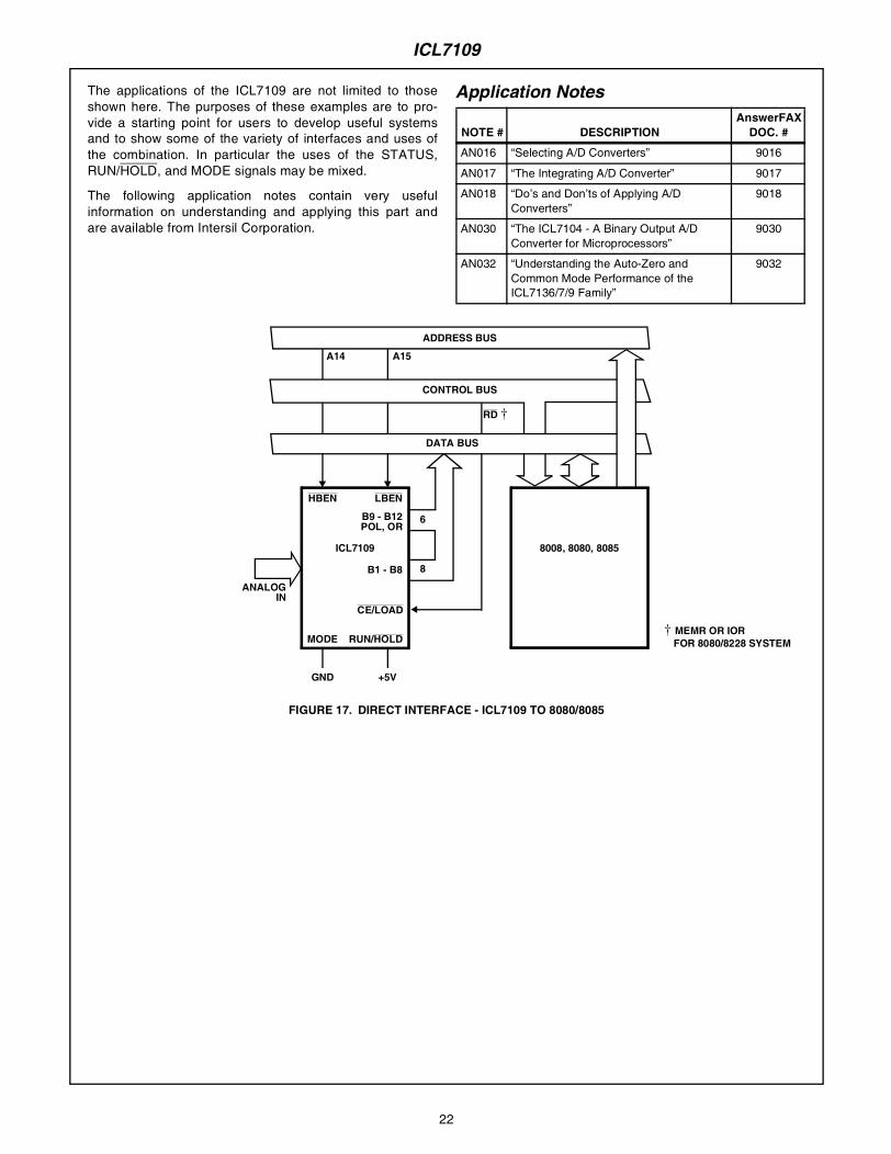
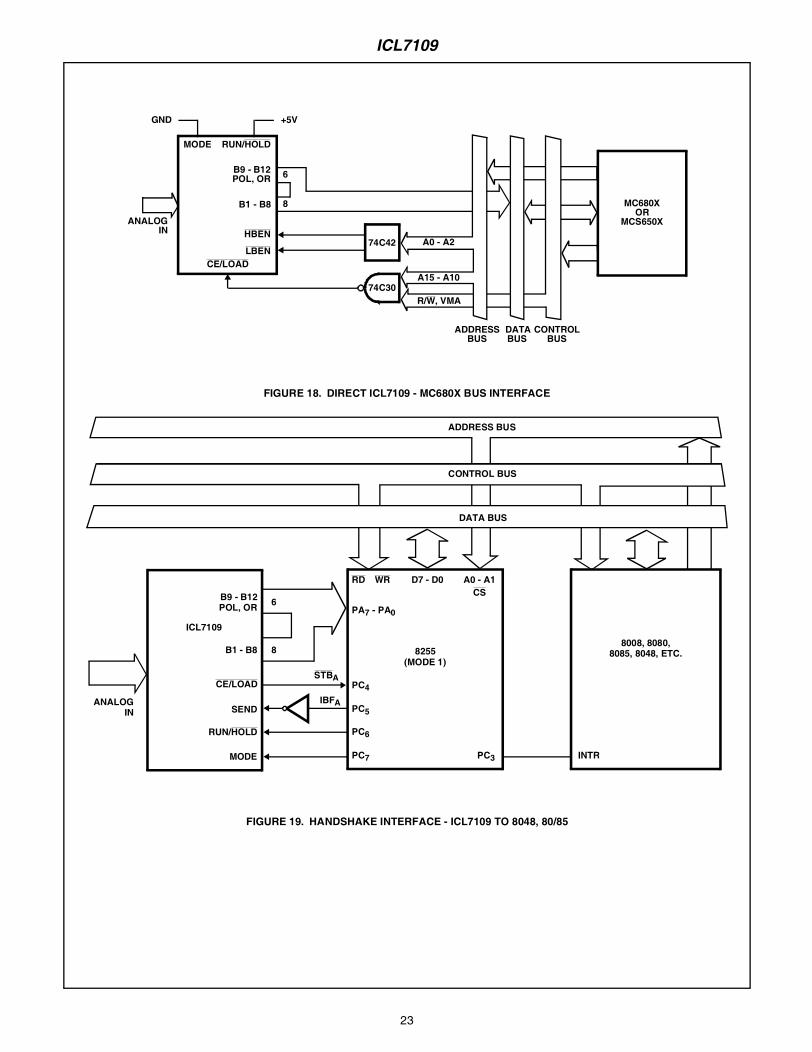
The three-state output capability of the ICL7109 allows directinterfacing to most microprocessor busses. Examples of thisare shown in Figures 17 and 18. It is necessary to carefullyconsider the system in this type of interface, to be sure thatrequirements for setup and hold times, and minimum pulsewidths are met. Note also the drive limitations on long buses.Generally this type of interface is only favored if the memoryperipheral address density is low so that simple addressdecoding can be used. Interrupt handling can also requiremany additional components, and using an interface devicewill usually simplify the system in this case.
13
1
2
3
4
5
6
7
8
9
10
11
12
14
15
16
17
18
19
20
GND
STATUS
POL
OR
B12
B11
B10
B9
B8
B7
B6
B5
B4
B3
B2
B1
TEST
LBEN
HBEN
CE/LOAD
28
40
39
38
37
36
35
34
33
32
31
30
29
27
26
25
24
23
22
21
V+
REF IN -
REF CAP-
REF CAP+
REF IN+
IN HI
IN LO
COMMON
INT
AZ
BUF
REF OUT
V-
SEND
RUN/HOLD
BUF OSC OUT
OSC SEL
OSC OUT
OSC IN
MODE
GND
HIGHORDER
BYTEOUTPUTS
LOWORDER
BYTEOUTPUTS
+5V
BYTECONTROL
INPUTS
GND
V+
+5V
1µF
0.01µF
0.33µF
0.15µFCAZ
CINT
RINT†
1MΩ R1
1kΩ
24kΩ
3.5795MHzTV CRYSTAL
†RINT = 20kΩ FOR 0.2V REF= 200kΩ FOR 2.0V REF
REF IN +
REF IN -
-
+
INPUT HIGH
INPUT LOW
GND
DIFFERENTIALREFERENCE
-5V
ICL7109
Handshake Mode Interfacing
The handshake mode allows ready interface with a widevariety of external devices. For instance, external latchesmay be clocked by the rising edge of CE/LOAD, and the byteenables may be used as byte identification flags or as loadenables.
Figure 19 shows a handshake interface to Intel microproces-sors again using an 8255PPI. The handshake operation withthe 8255 is controlled by inverting its Input Buffer Full (IBF)flag to drive the SEND input to the ICL7109, and using theCE/LOAD to drive the 8255 strobe. The internal control reg-ister of the PPI should be sent in MODE 1 for the port used.If the ICL7109 is in handshake mode and the 8255 IBF flagis low, the next word will be strobed into the port. The strobewill cause IBF to go high (SEND goes low), which will keepthe enable byte outputs active. The PPI will generate aninterrupt which when executed will result in the data beingread. When the byte is read, the IBF will be reset low, whichcauses the ICL7109 to sequence into the next byte. This fig-ure shows the MODE input to the ICL7109 connected to acontrol line on the PPI. If this output is left high, or tied highseparately, the data from every conversion (provided thedata access takes less time than a conversion) will besequenced in two bytes into the system.
If this output is made to go from low to high, the outputsequence can be obtained on demand, and the interruptmay be used to reset the MODE bit. Note that theRUN/HOLD input to the ICL7109 may also be obtained oncommand under software control. Note that one port of the
8255 is not used, and can service another peripheral device.the same arrangement can also be used with the 8155.
Figure 20 shows a similar arrangement with the MC6800 orMCS650X microprocessors, except that both MODE andRUN/HOLD are tied high to save port outputs.
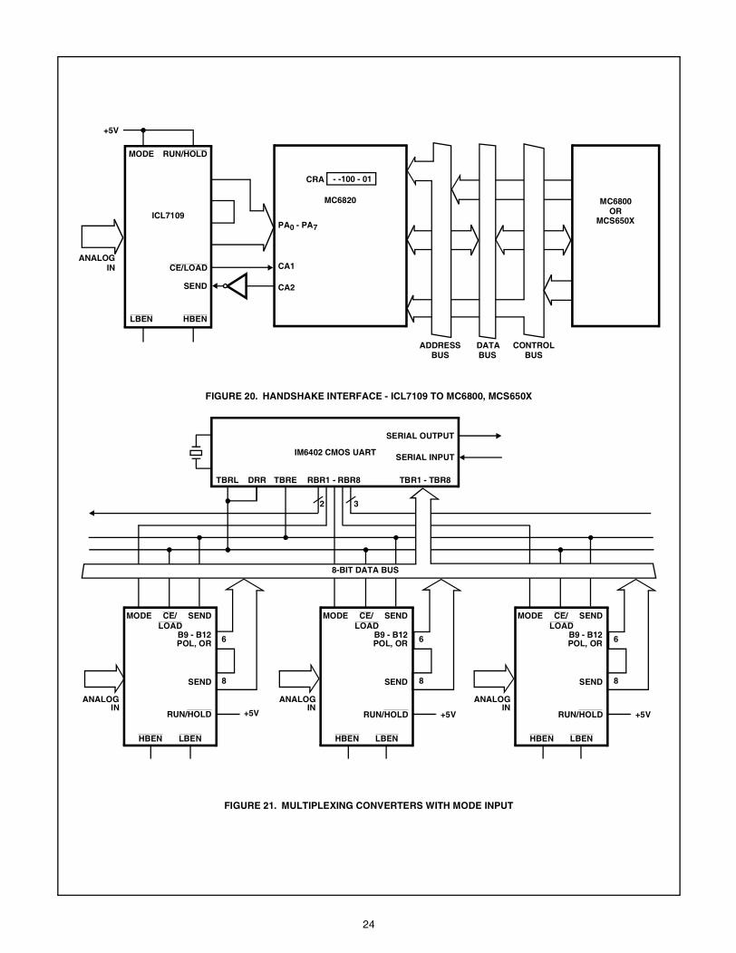
The handshake mode is particularly convenient for directlyinterfacing to industry standard UARTs (such as the IntersilIM6402 or Western Digital TR1602) providing a minimumcomponent count means of serially transmitting converteddata. A typical UART connection is shown in Figure 1A. Inthis circuit, any word received by the UART causes theUART DR (Data Ready) output to go high. This drives theMODE input to the ICL7109 high, triggering the ICL7109 intohandshake mode. The high order byte is output to the UARTfirst, and when the UART has transferred the data to theTransmitter Register, TBRE (SEND) goes high again, LBENwill go high, driving the UART DRR (Data Ready Reset)which will signal the end of the transfer of data from theICL7109 to the UART.
Figure 21 shows an extension of the one converter oneUART scheme to several ICL7109s with one UART. In thiscircuit, the word received by the UART (available at the RBRoutputs when DR is high) is used to select which converterwill handshake with the UART. With no external compo-nents, this scheme will allow up to eight ICL7109s to inter-face with one UART. Using a few more components todecode the received word will allow up to 256 converters tobe accessed on one serial line.
MC6820
GND
MODE
ICL7109
B9 - B12POL, OR
B1 - B8
STATUS
RUN/HOLD
LBENHBENLOADCE/
GND
ANALOGIN
PA0 - 5
PB0 - 7
CB1
CB2
CRB - -11R-01MC680X
ORMCS650X
ADDRESSBUS
DATABUS
CONTROLBUS
6
8
FIGURE 16. FULL-TIME PARALLEL INTERFACE TO MC680X OR MCS650X MICROPROCESSORS
ICL7109
21
22
The applications of the ICL7109 are not limited to thoseshown here. The purposes of these examples are to pro-vide a starting point for users to develop useful systemsand to show some of the variety of interfaces and uses ofthe combination. In particular the uses of the STATUS,RUN/HOLD, and MODE signals may be mixed.
The following application notes contain very usefulinformation on understanding and applying this part andare available from Intersil Corporation.
Application Notes
NOTE # DESCRIPTIONAnswerFAX
DOC. #
AN016 “Selecting A/D Converters” 9016
AN017 “The Integrating A/D Converter” 9017
AN018 “Do’s and Don’ts of Applying A/D Converters”
9018
AN030 “The ICL7104 - A Binary Output A/D Converter for Microprocessors”
9030
AN032 “Understanding the Auto-Zero and Common Mode Performance of the ICL7136/7/9 Family”
9032
FIGURE 17. DIRECT INTERFACE - ICL7109 TO 8080/8085
MODE
ICL7109
B9 - B12
B1 - B8
RUN/HOLD
LBENHBEN
GND
ANALOGIN
+5V
POL, OR6
8
CE/LOAD
A14 A15
ADDRESS BUS
CONTROL BUS
RD †
DATA BUS
8008, 8080, 8085
† MEMR OR IORFOR 8080/8228 SYSTEM
ICL7109
23
FIGURE 18. DIRECT ICL7109 - MC680X BUS INTERFACE
FIGURE 19. HANDSHAKE INTERFACE - ICL7109 TO 8048, 80/85
74C42
74C30
MC680XOR
MCS650X
CONTROLBUS
DATABUS
ADDRESSBUS
A0 - A2
A15 - A10
R/W, VMA
CE/LOAD
MODE RUN/HOLD
B9 - B12POL, OR
B1 - B8
HBEN
LBEN
ANALOGIN
6
8
GND +5V
ANALOGIN
6
8
STBA
IBFA
B9 - B12POL, OR
ICL7109
B1 - B8
SEND
RUN/HOLD
MODE
CE/LOAD
RD WR D7 - D0 A0 - A1CS
8255(MODE 1)
PC4
PC5
PC6
PC7
PA7 - PA0
PC3
ADDRESS BUS
CONTROL BUS
DATA BUS
INTR
8008, 8080,8085, 8048, ETC.
ICL7109
24
FIGURE 20. HANDSHAKE INTERFACE - ICL7109 TO MC6800, MCS650X
FIGURE 21. MULTIPLEXING CONVERTERS WITH MODE INPUT
ANALOGIN
HBEN
ICL7109
LBEN
SEND
RUN/HOLDMODE
CE/LOAD
CRA
MC6820
CA1
CA2
PA0 - PA7
- -100 - 01
MC6800OR
MCS650X
ADDRESSBUS
DATABUS
CONTROLBUS
+5V
MODE SENDCE/LOAD
B9 - B12POL, OR
SEND
RUN/HOLD
HBEN LBEN
ANALOGIN
+5V
MODE SENDCE/LOAD
B9 - B12POL, OR
SEND
RUN/HOLD
HBEN LBEN
ANALOGIN
+5V
MODE SENDCE/LOAD
B9 - B12POL, OR
SEND
HBEN LBEN
ANALOGIN
6
8
6
8
6
8
TBRL DRR TBRE RBR1 - RBR8 TBR1 - TBR8
SERIAL INPUT
SERIAL OUTPUT
IM6402 CMOS UART
2 3
8-BIT DATA BUS
RUN/HOLD +5V
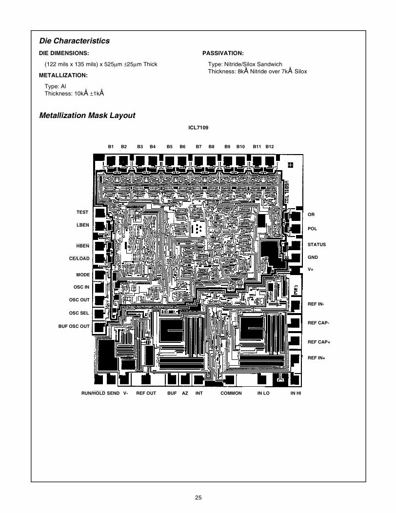
Die Characteristics
DIE DIMENSIONS:
(122 mils x 135 mils) x 525µm ±25µm Thick
METALLIZATION:
Type: AlThickness: 10kÅ ±1kÅ
PASSIVATION:
Type: Nitride/Silox SandwichThickness: 8kÅ Nitride over 7kÅ Silox
Metallization Mask LayoutICL7109
B1 B2 B3 B4 B5 B6 B7 B8 B9 B10 B11 B12
OR
POL
STATUS
GND
REF IN-
REF CAP-
REF CAP+
REF IN+
IN HIIN LOCOMMONINTAZBUFREF OUTSEND V-RUN/HOLD
TEST
LBEN
HBEN
CE/LOAD
MODE
OSC IN
OSC OUT
OSC SEL
BUF OSC OUT
V+
25