Embed Size (px)
Citation preview
© July 2010 Altera Corporation
SIII51013-1.9
13. IEEE 1149.1 (JTAG) Boundary-ScanTesting in Stratix III Devices
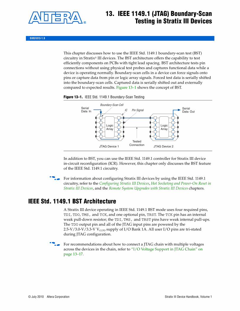
This chapter discusses how to use the IEEE Std. 1149.1 boundary-scan test (BST) circuitry in Stratix® III devices. The BST architecture offers the capability to test efficiently components on PCBs with tight lead spacing. BST architecture tests pin connections without using physical test probes and captures functional data while a device is operating normally. Boundary-scan cells in a device can force signals onto pins or capture data from pin or logic array signals. Forced test data is serially shifted into the boundary-scan cells. Captured data is serially shifted out and externally compared to expected results. Figure 13–1 shows the concept of BST.
In addition to BST, you can use the IEEE Std. 1149.1 controller for Stratix III device in-circuit reconfiguration (ICR). However, this chapter only discusses the BST feature of the IEEE Std. 1149.1 circuitry.
f For information about configuring Stratix III devices by using the IEEE Std. 1149.1 circuitry, refer to the Configuring Stratix III Devices, Hot Socketing and Power-On Reset in Stratix III Devices, and the Remote System Upgrades with Stratix III Devices chapters.
IEEE Std. 1149.1 BST Architecture A Stratix III device operating in IEEE Std. 1149.1 BST mode uses four required pins, TDI, TDO, TMS, and TCK, and one optional pin, TRST. The TCK pin has an internal weak pull-down resistor; the TDI, TMS, and TRST pins have weak internal pull-ups. The TDO output pin and all of the JTAG input pins are powered by the 2.5-V/3.0-V/3.3-V VCCPD supply of I/O Bank 1A. All user I/O pins are tri-stated during JTAG configuration.
f For recommendations about how to connect a JTAG chain with multiple voltages across the devices in the chain, refer to “I/O Voltage Support in JTAG Chain” on page 13–17.
Figure 13–1. IEEE Std. 1149.1 Boundary-Scan Testing
SerialData In
Boundary-Scan Cell
IC
LogicArray
SerialData Out
JTAG Device 1 JTAG Device 2
Pin Signal
TestedConnection
LogicArray
Stratix III Device Handbook, Volume 1
13–2 Chapter 13: IEEE 1149.1 (JTAG) Boundary-Scan Testing in Stratix III DevicesIEEE Std. 1149.1 BST Architecture
Table 13–1 summarizes the functions of each of these pins.
The IEEE Std. 1149.1 BST circuitry requires the following registers:
■ The instruction register determines the action to be performed and the data register to be accessed.
■ The bypass register is a one-bit-long data register that provides a minimum-length serial path between TDI and TDO.
■ The boundary-scan register is a shift register composed of all the boundary-scan cells of the device.
Table 13–1. IEEE Std. 1149.1 Pin Descriptions
Pin Description Function
TDI Test data inputSerial input pin for instructions as well as test and programming data. Signal applied to TDI is expected to change state at the falling edge of TCK. Data is shifted in on the rising edge of TCK.
TDO Test data outputSerial data output pin for instructions as well as test and programming data. Data is shifted out on the falling edge of TCK. The pin is tri-stated if data is not being shifted out of the device.
TMS Test mode select
Input pin that provides the control signal to determine the transitions of the test access port (TAP) controller state machine. Transitions within the state machine occur at the rising edge of TCK. Therefore, you must set up TMS before the rising edge of TCK. TMS is evaluated on the rising edge of TCK. During non-JTAG operation, Altera recommends you drive TMS high.
TCK Test clock input The clock input to the BST circuitry. Some operations occur at the rising edge, while others occur at the falling edge.
TRST (1) Test reset input (optional)
Active-low input to asynchronously reset the boundary-scan circuit. For non-JTAG users, you should permanently tie the pin to GND.
Note to Table 13–1:
(1) The minimum TRST pulse width to reset the JTAG TAP controller is 60 ns.
Stratix III Device Handbook, Volume 1 © July 2010 Altera Corporation
Chapter 13: IEEE 1149.1 (JTAG) Boundary-Scan Testing in Stratix III Devices 13–3IEEE Std. 1149.1 BST Architecture
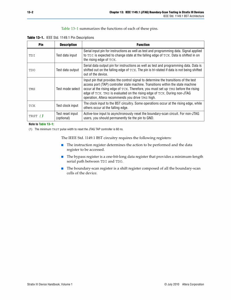
Figure 13–2 shows a functional model of the IEEE Std. 1149.1 circuitry.
IEEE Std. 1149.1 boundary-scan testing is controlled by a TAP controller. For more information about the TAP controller, refer to “IEEE Std. 1149.1 BST Operation Control” on page 13–7. The TMS and TCK pins operate the TAP controller. The TDI and TDO pins provide the serial path for the data registers. The TDI pin also provides data to the instruction register, which then generates control logic for the data registers.
Figure 13–2. IEEE Std. 1149.1 Circuitry
Note to Figure 13–2:(1) For register lengths, refer to the device datasheet in the Configuring Stratix III Devices chapter in volume 1 of the Stratix III Device Handbook.
a
UPDATEIRCLOCKIR
SHIFTIR
UPDATEDRCLOCKDR
SHIFTDR
TDI
Instruction Register
Bypass Register
Boundary-Scan Register
Instruction Decode
TMS
TCLK
TAPController
ICR Registers
TDO
Data Registers
Device ID Register
TRST
(1)
(1)
© July 2010 Altera Corporation Stratix III Device Handbook, Volume 1
13–4 Chapter 13: IEEE 1149.1 (JTAG) Boundary-Scan Testing in Stratix III DevicesIEEE Std. 1149.1 Boundary-Scan Register
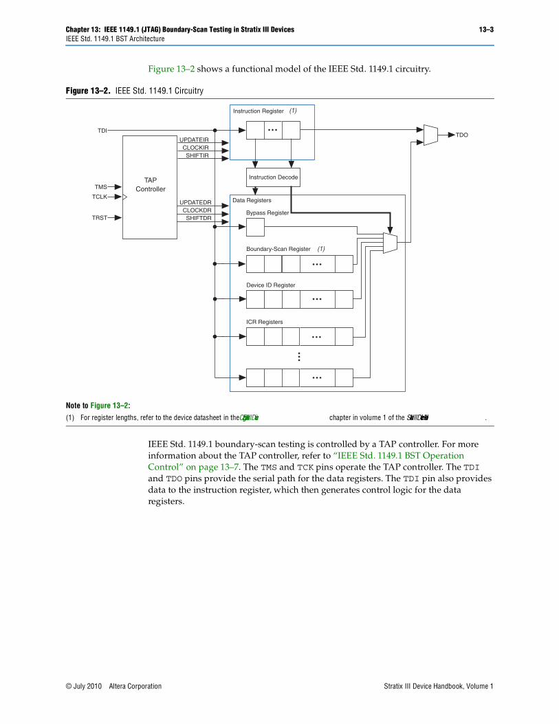
IEEE Std. 1149.1 Boundary-Scan Register The boundary-scan register is a large serial shift register that uses the TDI pin as an input and the TDO pin as an output. The boundary-scan register consists of three-bit peripheral elements that are associated with Stratix III I/O pins. You can use the boundary-scan register to test external pin connections or to capture internal data.
f For the Stratix III family device boundary-scan register lengths, refer to the Configuring Stratix III Devices chapter in volume 1 of the Stratix III Device Handbook.
Figure 13–3 shows how test data is serially shifted around the periphery of the IEEE Std. 1149.1 device.
Table 13–2 lists the boundary-scan register length for Stratix III devices.
Figure 13–3. Boundary-Scan Register
Table 13–2. Stratix III Boundary-Scan Register Length
Device Boundary-Scan Register Length
EP3SL50 1506
EP3SL70 1506
EP3SL110 2274
EP3SL150ES 2274
EP3SL150 2274
EP3SL200 2970
EP3SL340 3402
EP3SE50 1506
EP3SE80 2274
EP3SE110 2274
EP3SE260 2970
TCK TRST TMS
TAP Controller
TDI
Internal Logic
TDO
Each peripheralelement is either anI/O pin, dedicatedinput pin, ordedicatedconfiguration pin.
Stratix III Device Handbook, Volume 1 © July 2010 Altera Corporation
Chapter 13: IEEE 1149.1 (JTAG) Boundary-Scan Testing in Stratix III Devices 13–5IEEE Std. 1149.1 Boundary-Scan Register
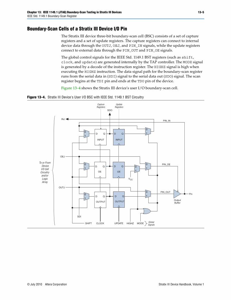
Boundary-Scan Cells of a Stratix III Device I/O PinThe Stratix III device three-bit boundary-scan cell (BSC) consists of a set of capture registers and a set of update registers. The capture registers can connect to internal device data through the OUTJ, OEJ, and PIN_IN signals, while the update registers connect to external data through the PIN_OUT and PIN_OE signals.
The global control signals for the IEEE Std. 1149.1 BST registers (such as shift, clock, and update) are generated internally by the TAP controller. The MODE signal is generated by a decode of the instruction register. The HIGHZ signal is high when executing the HIGHZ instruction. The data signal path for the boundary-scan register runs from the serial data in (SDI) signal to the serial data out (SDO) signal. The scan register begins at the TDI pin and ends at the TDO pin of the device.
Figure 13–4 shows the Stratix III device's user I/O boundary-scan cell.
Figure 13–4. Stratix III Device's User I/O BSC with IEEE Std. 1149.1 BST Circuitry
0
1
D Q
OUTPUT
D Q
OE
D Q
INPUT
D Q
INPUT
D Q
OUTPUT
D Q
OE
To or From DeviceI/O CellCircuitryand/orLogicArray
0
1
0
10
1
0
10
1
0
1
PIN_OUT
INJ
OEJ
OUTJ
VCC
SDO
Pin
SHIFT
SDI
CLOCK UPDATE HIGHZ MODE
PIN_OE
PIN_IN
OutputBuffer
CaptureRegisters
UpdateRegisters
GlobalSignals
© July 2010 Altera Corporation Stratix III Device Handbook, Volume 1
13–6 Chapter 13: IEEE 1149.1 (JTAG) Boundary-Scan Testing in Stratix III DevicesIEEE Std. 1149.1 Boundary-Scan Register
Table 13–3 lists the capture and update register capabilities of all boundary-scan cells within Stratix III devices.
Table 13–3. Stratix III Device Boundary Scan Cell Descriptions (Note 1)
Pin Type
Captures Drives
CommentsOutput Capture Register
OE Capture Register
Input Capture Register
Output Update
Register
OE Update Register
Input Update
Register
User I/O pins OUTJ OEJ PIN_IN PIN_OUT PIN_OE INJ —
Dedicated clock input 0 1 PIN_IN — — —
PIN_IN drives to clock network or logic array
Dedicated input (2) 0 1 PIN_IN — — — PIN_IN drives to
control logic
Dedicated bi-directional (open drain) (3)
0 OEJ PIN_IN — — — PIN_IN drives to configuration control
Dedicated bi-directional (4) OUTJ OEJ PIN_IN — — —
PIN_IN drives to configuration control and OUTJ drives to output buffer
Dedicated output (5) OUTJ 0 0 — — — OUTJ drives to
output buffer
Notes to Table 13–3:
(1) TDI, TDO, TMS, TCK, TRST, all VCC and GND pin types, VREF, and TEMP_DIODE pins do not have BSCs.(2) This includes pins PLL_ENA, nCONFIG, MSEL0, MSEL1, MSEL2, nCE, PORSEL, and nIO_PULLUP.(3) This includes pins CONF_DONE and nSTATUS.(4) This includes pin DCLK.(5) This includes pin nCEO.
Stratix III Device Handbook, Volume 1 © July 2010 Altera Corporation
Chapter 13: IEEE 1149.1 (JTAG) Boundary-Scan Testing in Stratix III Devices 13–7IEEE Std. 1149.1 BST Operation Control
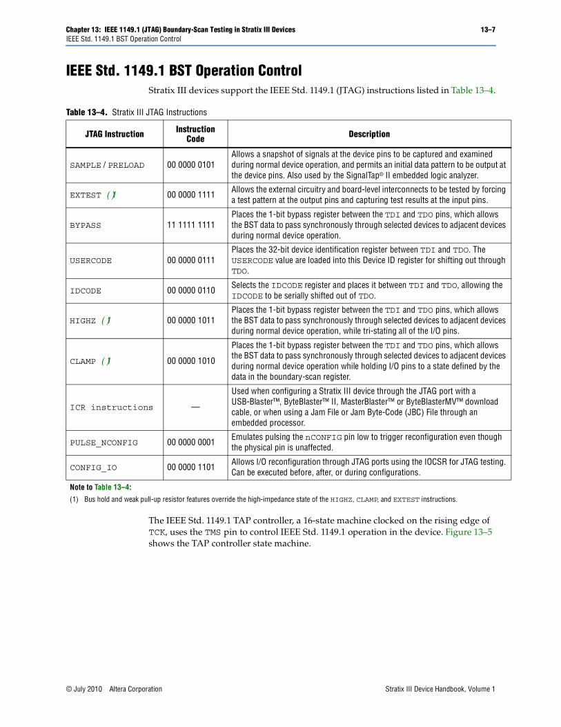
IEEE Std. 1149.1 BST Operation Control Stratix III devices support the IEEE Std. 1149.1 (JTAG) instructions listed in Table 13–4.
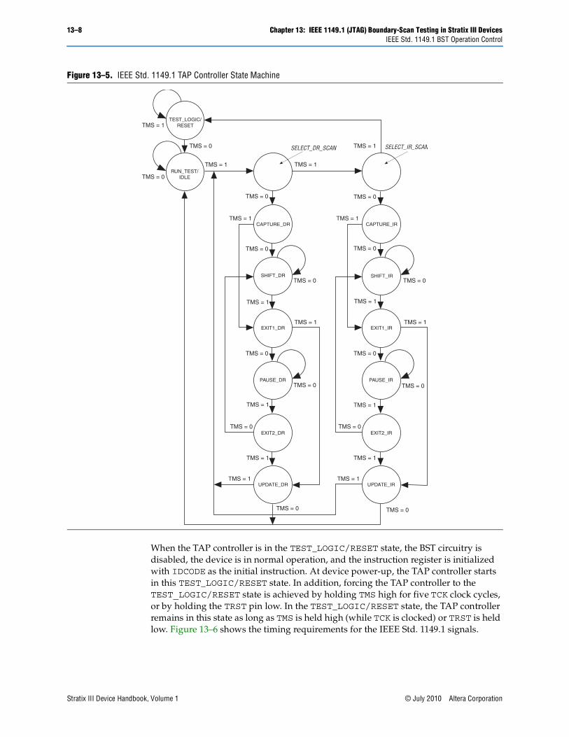
The IEEE Std. 1149.1 TAP controller, a 16-state machine clocked on the rising edge of TCK, uses the TMS pin to control IEEE Std. 1149.1 operation in the device. Figure 13–5 shows the TAP controller state machine.
Table 13–4. Stratix III JTAG Instructions
JTAG Instruction Instruction Code Description
SAMPLE / PRELOAD 00 0000 0101Allows a snapshot of signals at the device pins to be captured and examined during normal device operation, and permits an initial data pattern to be output atthe device pins. Also used by the SignalTap® II embedded logic analyzer.
EXTEST (1) 00 0000 1111 Allows the external circuitry and board-level interconnects to be tested by forcinga test pattern at the output pins and capturing test results at the input pins.
BYPASS 11 1111 1111Places the 1-bit bypass register between the TDI and TDO pins, which allows the BST data to pass synchronously through selected devices to adjacent devicesduring normal device operation.
USERCODE 00 0000 0111Places the 32-bit device identification register between TDI and TDO. The USERCODE value are loaded into this Device ID register for shifting out throughTDO.
IDCODE 00 0000 0110 Selects the IDCODE register and places it between TDI and TDO, allowing the IDCODE to be serially shifted out of TDO.
HIGHZ (1) 00 0000 1011Places the 1-bit bypass register between the TDI and TDO pins, which allows the BST data to pass synchronously through selected devices to adjacent devicesduring normal device operation, while tri-stating all of the I/O pins.
CLAMP (1) 00 0000 1010
Places the 1-bit bypass register between the TDI and TDO pins, which allows the BST data to pass synchronously through selected devices to adjacent devicesduring normal device operation while holding I/O pins to a state defined by the data in the boundary-scan register.
ICR instructions —
Used when configuring a Stratix III device through the JTAG port with a USB-Blaster™, ByteBlaster™ II, MasterBlaster™ or ByteBlasterMV™ download cable, or when using a Jam File or Jam Byte-Code (JBC) File through an embedded processor.
PULSE_NCONFIG 00 0000 0001 Emulates pulsing the nCONFIG pin low to trigger reconfiguration even though the physical pin is unaffected.
CONFIG_IO 00 0000 1101 Allows I/O reconfiguration through JTAG ports using the IOCSR for JTAG testing.Can be executed before, after, or during configurations.
Note to Table 13–4:(1) Bus hold and weak pull-up resistor features override the high-impedance state of the HIGHZ, CLAMP, and EXTEST instructions.
© July 2010 Altera Corporation Stratix III Device Handbook, Volume 1
13–8 Chapter 13: IEEE 1149.1 (JTAG) Boundary-Scan Testing in Stratix III DevicesIEEE Std. 1149.1 BST Operation Control
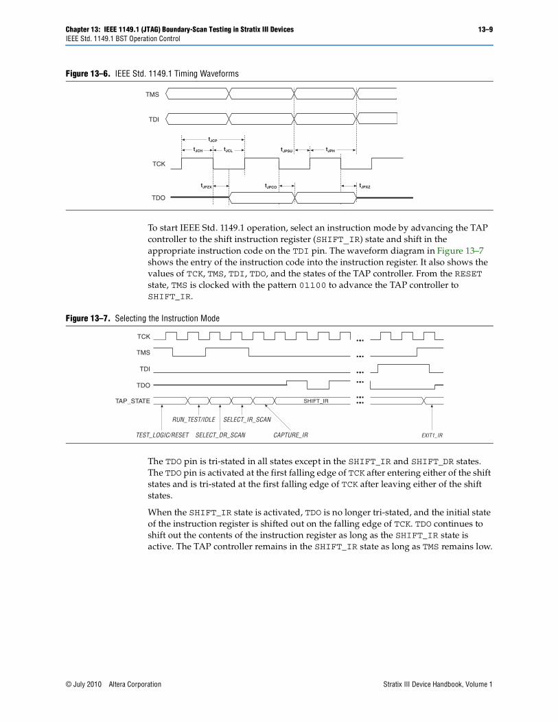
When the TAP controller is in the TEST_LOGIC/RESET state, the BST circuitry is disabled, the device is in normal operation, and the instruction register is initialized with IDCODE as the initial instruction. At device power-up, the TAP controller starts in this TEST_LOGIC/RESET state. In addition, forcing the TAP controller to the TEST_LOGIC/RESET state is achieved by holding TMS high for five TCK clock cycles, or by holding the TRST pin low. In the TEST_LOGIC/RESET state, the TAP controller remains in this state as long as TMS is held high (while TCK is clocked) or TRST is held low. Figure 13–6 shows the timing requirements for the IEEE Std. 1149.1 signals.
Figure 13–5. IEEE Std. 1149.1 TAP Controller State Machine
SELECT_DR_SCAN
CAPTURE_DR
SHIFT_DR
EXIT1_DR
PAUSE_DR
EXIT2_DR
UPDATE_DR
SHIFT_IR
EXIT1_IR
PAUSE_IR
EXIT2_IR
UPDATE_IR
TMS = 0
TMS = 0
TMS = 0
TMS = 1
TMS = 0
TMS = 1
TMS = 1
TMS = 0
TMS = 1
TMS = 0
TMS = 1
TMS = 1
TMS = 0TMS = 0
TMS = 1
TMS = 1
TMS = 0
TMS = 1
TMS = 0
TMS = 0
TMS = 1
TMS = 0
TMS = 0
TMS = 1
TMS = 0
RUN_TEST/IDLETMS = 0
TEST_LOGIC/RESETTMS = 1
TMS = 0
TMS = 1 TMS = 1
TMS = 1 TMS = 1
CAPTURE_IR
SELECT_IR_SCAN
Stratix III Device Handbook, Volume 1 © July 2010 Altera Corporation
Chapter 13: IEEE 1149.1 (JTAG) Boundary-Scan Testing in Stratix III Devices 13–9IEEE Std. 1149.1 BST Operation Control
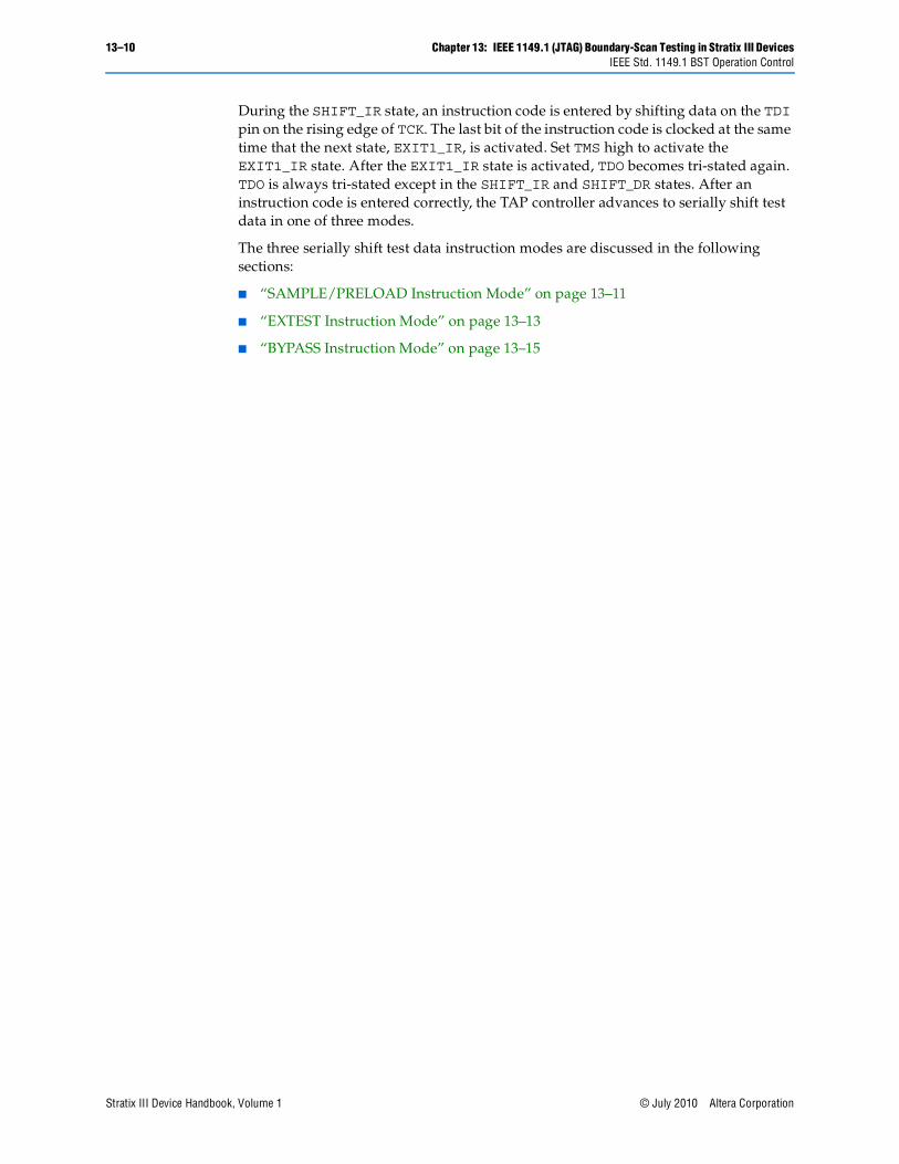
To start IEEE Std. 1149.1 operation, select an instruction mode by advancing the TAP controller to the shift instruction register (SHIFT_IR) state and shift in the appropriate instruction code on the TDI pin. The waveform diagram in Figure 13–7 shows the entry of the instruction code into the instruction register. It also shows the values of TCK, TMS, TDI, TDO, and the states of the TAP controller. From the RESET state, TMS is clocked with the pattern 01100 to advance the TAP controller to SHIFT_IR.
The TDO pin is tri-stated in all states except in the SHIFT_IR and SHIFT_DR states. The TDO pin is activated at the first falling edge of TCK after entering either of the shift states and is tri-stated at the first falling edge of TCK after leaving either of the shift states.
When the SHIFT_IR state is activated, TDO is no longer tri-stated, and the initial state of the instruction register is shifted out on the falling edge of TCK. TDO continues to shift out the contents of the instruction register as long as the SHIFT_IR state is active. The TAP controller remains in the SHIFT_IR state as long as TMS remains low.
Figure 13–6. IEEE Std. 1149.1 Timing Waveforms
TDO
TCK
tJPZX tJPCO
tJPH
tJPXZ
tJCP
tJPSU tJCL tJCH
TDI
TMS
Figure 13–7. Selecting the Instruction Mode
TCK
TMS
TDI
TDO
TAP_STATE SHIFT_IR
RUN_TEST/IDLE SELECT_IR_SCAN
SELECT_DR_SCANTEST_LOGIC/RESET CAPTURE_IR EXIT1_IR
© July 2010 Altera Corporation Stratix III Device Handbook, Volume 1
13–10 Chapter 13: IEEE 1149.1 (JTAG) Boundary-Scan Testing in Stratix III DevicesIEEE Std. 1149.1 BST Operation Control
During the SHIFT_IR state, an instruction code is entered by shifting data on the TDI pin on the rising edge of TCK. The last bit of the instruction code is clocked at the same time that the next state, EXIT1_IR, is activated. Set TMS high to activate the EXIT1_IR state. After the EXIT1_IR state is activated, TDO becomes tri-stated again. TDO is always tri-stated except in the SHIFT_IR and SHIFT_DR states. After an instruction code is entered correctly, the TAP controller advances to serially shift test data in one of three modes.
The three serially shift test data instruction modes are discussed in the following sections:
■ “SAMPLE/PRELOAD Instruction Mode” on page 13–11
■ “EXTEST Instruction Mode” on page 13–13
■ “BYPASS Instruction Mode” on page 13–15
Stratix III Device Handbook, Volume 1 © July 2010 Altera Corporation
Chapter 13: IEEE 1149.1 (JTAG) Boundary-Scan Testing in Stratix III Devices 13–11IEEE Std. 1149.1 BST Operation Control
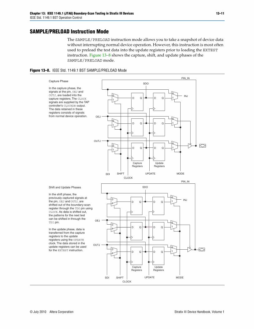
SAMPLE/PRELOAD Instruction Mode The SAMPLE/PRELOAD instruction mode allows you to take a snapshot of device data without interrupting normal device operation. However, this instruction is most often used to preload the test data into the update registers prior to loading the EXTEST instruction. Figure 13–8 shows the capture, shift, and update phases of the SAMPLE/PRELOAD mode.
Figure 13–8. IEEE Std. 1149.1 BST SAMPLE/PRELOAD Mode
1
0
D Q D Q 1
0
1
0
1
0D Q D Q 1
0
D Q D Q 1
0
OUTJ
OEJ
MODE
INJ
CaptureRegisters
UpdateRegisters
SDI SHIFT
CLOCK
UPDATE
SDO
1
0
D Q D Q 1
0
1
0
1
0D Q D Q 1
0
D Q D Q 1
0
OUTJ
OEJ
MODE
INJ
CaptureRegisters
UpdateRegisters
SDI SHIFT
CLOCK
UPDATE
SDO
PIN_IN
PIN_INCapture Phase
In the capture phase, thesignals at the pin, OEJ and OUTJ, are loaded into thecapture registers. The CLOCKsignals are supplied by the TAPcontroller's CLOCKDR output.The data retained in theseregisters consists of signals from normal device operation.
Shift and Update Phases
In the shift phase, thepreviously captured signals atthe pin, OEJ and OUTJ, are shifted out of the boundary-scanregister through the TDO pin usingCLOCK. As data is shifted out,the patterns for the next test can be shifted in through theTDI pin.
In the update phase, data is transferred from the captureregisters to the updateregisters using the UPDATEclock. The data stored in theupdate registers can be used for the EXTEST instruction.
© July 2010 Altera Corporation Stratix III Device Handbook, Volume 1
13–12 Chapter 13: IEEE 1149.1 (JTAG) Boundary-Scan Testing in Stratix III DevicesIEEE Std. 1149.1 BST Operation Control
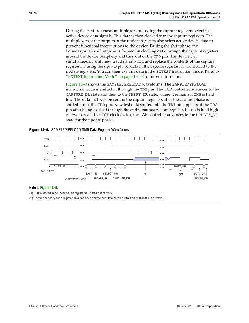
During the capture phase, multiplexers preceding the capture registers select the active device data signals. This data is then clocked into the capture registers. The multiplexers at the outputs of the update registers also select active device data to prevent functional interruptions to the device. During the shift phase, the boundary-scan shift register is formed by clocking data through the capture registers around the device periphery and then out of the TDO pin. The device can simultaneously shift new test data into TDI and replace the contents of the capture registers. During the update phase, data in the capture registers is transferred to the update registers. You can then use this data in the EXTEST instruction mode. Refer to “EXTEST Instruction Mode” on page 13–13 for more information.
Figure 13–9 shows the SAMPLE/PRELOAD waveforms. The SAMPLE/PRELOAD instruction code is shifted in through the TDI pin. The TAP controller advances to the CAPTURE_DR state and then to the SHIFT_DR state, where it remains if TMS is held low. The data that was present in the capture registers after the capture phase is shifted out of the TDO pin. New test data shifted into the TDI pin appears at the TDO pin after being clocked through the entire boundary-scan register. If TMS is held high on two consecutive TCK clock cycles, the TAP controller advances to the UPDATE_DR state for the update phase.
Figure 13–9. SAMPLE/PRELOAD Shift Data Register Waveforms
Note to Figure 13–9:
(1) Data stored in boundary-scan register is shifted out of TDO.(2) After boundary-scan register data has been shifted out, data entered into TDI will shift out of TDO.
(1) (2)UPDATE_IR
SHIFT_DR
EXIT1_DRSELECT_DR
CAPTURE_DR
EXIT1_IR
UPDATE_DR
SHIFT_IR
Instruction Code
TCK
TMS
TDI
TDO
TAP_STATE
Stratix III Device Handbook, Volume 1 © July 2010 Altera Corporation
Chapter 13: IEEE 1149.1 (JTAG) Boundary-Scan Testing in Stratix III Devices 13–13IEEE Std. 1149.1 BST Operation Control
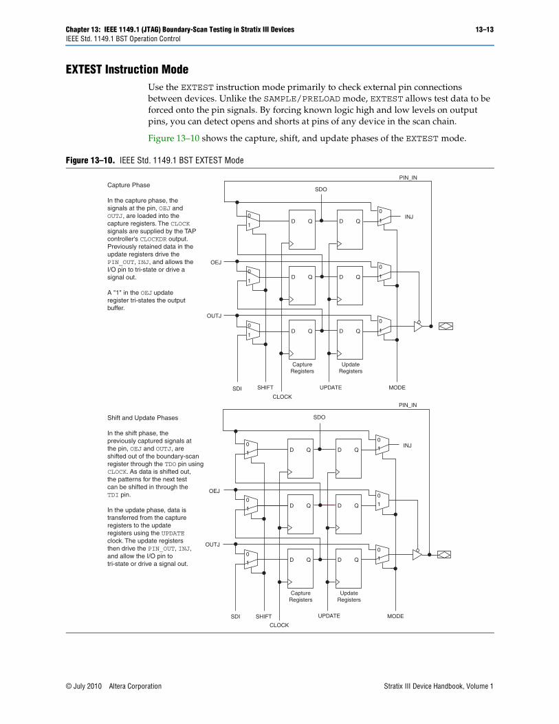
EXTEST Instruction ModeUse the EXTEST instruction mode primarily to check external pin connections between devices. Unlike the SAMPLE/PRELOAD mode, EXTEST allows test data to be forced onto the pin signals. By forcing known logic high and low levels on output pins, you can detect opens and shorts at pins of any device in the scan chain.
Figure 13–10 shows the capture, shift, and update phases of the EXTEST mode.
Figure 13–10. IEEE Std. 1149.1 BST EXTEST Mode
1
0
D Q D Q 1
0
1
0
1
0D Q D Q 1
0
D Q D Q 1
0
OUTJ
OEJ
MODE
INJ
CaptureRegisters
UpdateRegisters
SDI SHIFT
CLOCK
UPDATE
SDO
1
0
D Q D Q 1
0
1
0
1
0D Q D Q 1
0
D Q D Q 1
0
OUTJ
OEJ
MODE
INJ
CaptureRegisters
UpdateRegisters
SDI SHIFT
CLOCK
UPDATE
SDO
PIN_IN
PIN_INCapture Phase
In the capture phase, thesignals at the pin, OEJ and OUTJ, are loaded into thecapture registers. The CLOCKsignals are supplied by the TAPcontroller's CLOCKDR output.Previously retained data in theupdate registers drive the PIN_OUT, INJ, and allows theI/O pin to tri-state or drive asignal out.
A "1" in the OEJ updateregister tri-states the outputbuffer.
Shift and Update Phases
In the shift phase, thepreviously captured signals atthe pin, OEJ and OUTJ, are shifted out of the boundary-scanregister through the TDO pin usingCLOCK. As data is shifted out,the patterns for the next test can be shifted in through theTDI pin.
In the update phase, data is transferred from the captureregisters to the updateregisters using the UPDATEclock. The update registersthen drive the PIN_OUT, INJ,and allow the I/O pin totri-state or drive a signal out.
© July 2010 Altera Corporation Stratix III Device Handbook, Volume 1
13–14 Chapter 13: IEEE 1149.1 (JTAG) Boundary-Scan Testing in Stratix III DevicesIEEE Std. 1149.1 BST Operation Control
EXTEST mode selects data differently than SAMPLE/PRELOAD mode. EXTEST chooses data from the update registers as the source of the output and output-enable signals. After the EXTEST instruction code is entered, the multiplexers select the update register data. Therefore, data stored in these registers from a previous EXTEST or SAMPLE/PRELOAD test cycle can be forced onto the pin signals. In the capture phase, the results of this test data are stored in the capture registers and then shifted out of TDO during the shift phase. You can then store new test data in the update registers during the update phase.
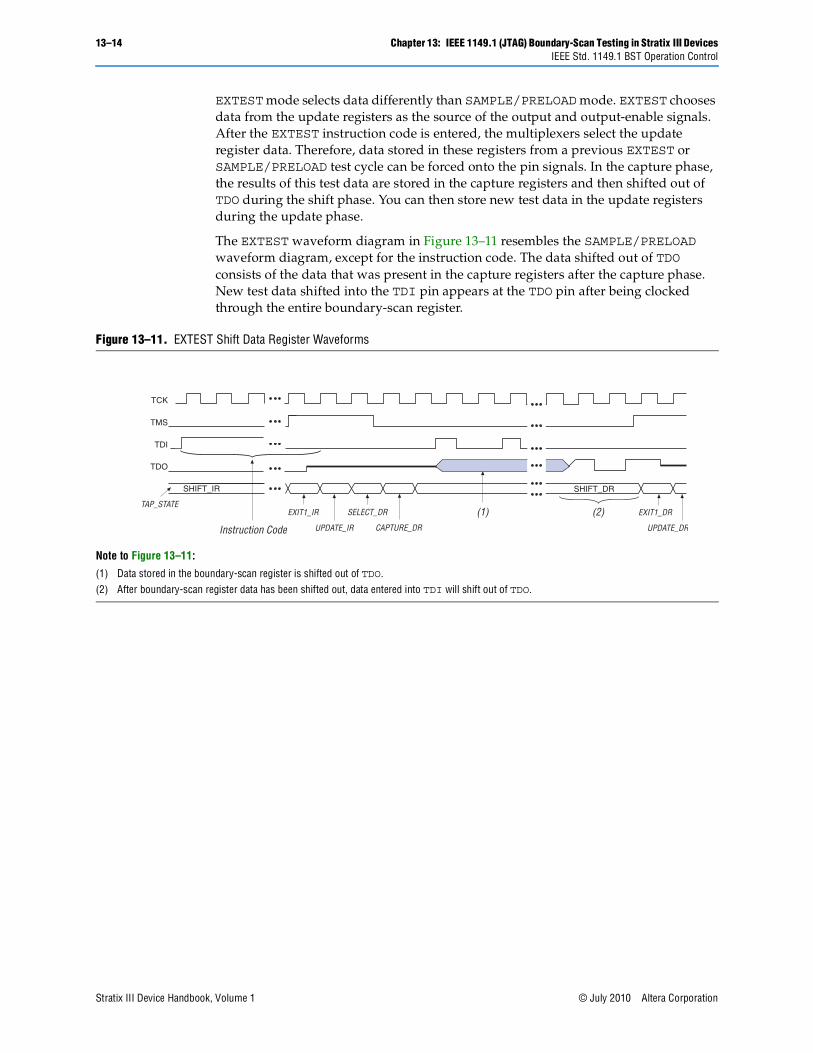
The EXTEST waveform diagram in Figure 13–11 resembles the SAMPLE/PRELOAD waveform diagram, except for the instruction code. The data shifted out of TDO consists of the data that was present in the capture registers after the capture phase. New test data shifted into the TDI pin appears at the TDO pin after being clocked through the entire boundary-scan register.
Figure 13–11. EXTEST Shift Data Register Waveforms
Note to Figure 13–11:
(1) Data stored in the boundary-scan register is shifted out of TDO.(2) After boundary-scan register data has been shifted out, data entered into TDI will shift out of TDO.
UPDATE_IR
SHIFT_DR
EXIT1_DRSELECT_DR
CAPTURE_DR
EXIT1_IR
UPDATE_DR
SHIFT_IR
Instruction Code
TCK
TMS
TDI
TDO
TAP_STATE(1) (2)
Stratix III Device Handbook, Volume 1 © July 2010 Altera Corporation
Chapter 13: IEEE 1149.1 (JTAG) Boundary-Scan Testing in Stratix III Devices 13–15IEEE Std. 1149.1 BST Operation Control
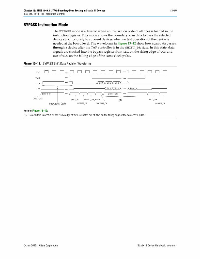
BYPASS Instruction ModeThe BYPASS mode is activated when an instruction code of all ones is loaded in the instruction register. This mode allows the boundary scan data to pass the selected device synchronously to adjacent devices when no test operation of the device is needed at the board level. The waveforms in Figure 13–12 show how scan data passes through a device after the TAP controller is in the SHIFT_DR state. In this state, data signals are clocked into the bypass register from TDI on the rising edge of TCK and out of TDO on the falling edge of the same clock pulse.
Figure 13–12. BYPASS Shift Data Register Waveforms
Note to Figure 13–12:
(1) Data shifted into TDI on the rising edge of TCK is shifted out of TDO on the falling edge of the same TCK pulse.
(1)UPDATE_IR
SELECT_DR_SCAN
CAPTURE_DR
EXIT1_IR EXIT1_DR
UPDATE_DR
SHIFT_DR
Instruction Code
TCK
TMS
TDI
TDO
TAP_STATE
SHIFT_IR
Bit 2 Bit 3
Bit 1 Bit 2 Bit 4
Bit 1
© July 2010 Altera Corporation Stratix III Device Handbook, Volume 1
13–16 Chapter 13: IEEE 1149.1 (JTAG) Boundary-Scan Testing in Stratix III DevicesIEEE Std. 1149.1 BST Operation Control
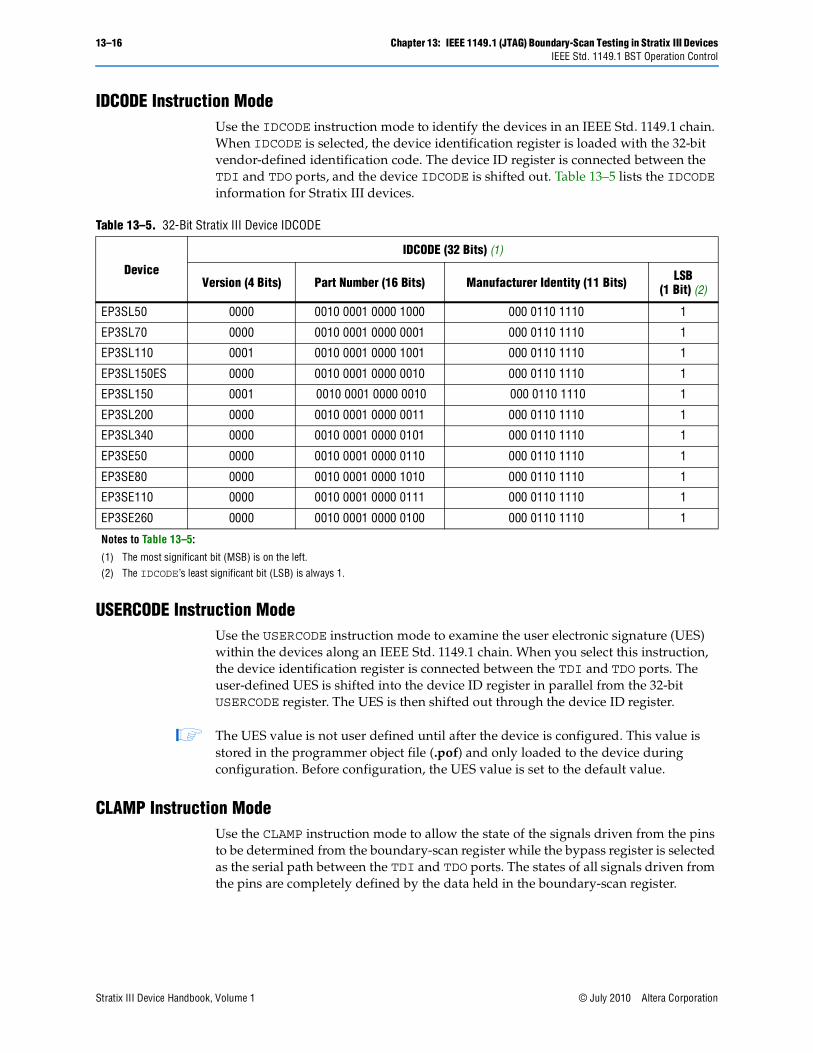
IDCODE Instruction ModeUse the IDCODE instruction mode to identify the devices in an IEEE Std. 1149.1 chain. When IDCODE is selected, the device identification register is loaded with the 32-bit vendor-defined identification code. The device ID register is connected between the TDI and TDO ports, and the device IDCODE is shifted out. Table 13–5 lists the IDCODE information for Stratix III devices.
USERCODE Instruction ModeUse the USERCODE instruction mode to examine the user electronic signature (UES) within the devices along an IEEE Std. 1149.1 chain. When you select this instruction, the device identification register is connected between the TDI and TDO ports. The user-defined UES is shifted into the device ID register in parallel from the 32-bit USERCODE register. The UES is then shifted out through the device ID register.
1 The UES value is not user defined until after the device is configured. This value is stored in the programmer object file (.pof) and only loaded to the device during configuration. Before configuration, the UES value is set to the default value.
CLAMP Instruction ModeUse the CLAMP instruction mode to allow the state of the signals driven from the pins to be determined from the boundary-scan register while the bypass register is selected as the serial path between the TDI and TDO ports. The states of all signals driven from the pins are completely defined by the data held in the boundary-scan register.
Table 13–5. 32-Bit Stratix III Device IDCODE
Device
IDCODE (32 Bits) (1)
Version (4 Bits) Part Number (16 Bits) Manufacturer Identity (11 Bits) LSB (1 Bit) (2)
EP3SL50 0000 0010 0001 0000 1000 000 0110 1110 1
EP3SL70 0000 0010 0001 0000 0001 000 0110 1110 1
EP3SL110 0001 0010 0001 0000 1001 000 0110 1110 1
EP3SL150ES 0000 0010 0001 0000 0010 000 0110 1110 1
EP3SL150 0001 0010 0001 0000 0010 000 0110 1110 1
EP3SL200 0000 0010 0001 0000 0011 000 0110 1110 1
EP3SL340 0000 0010 0001 0000 0101 000 0110 1110 1
EP3SE50 0000 0010 0001 0000 0110 000 0110 1110 1
EP3SE80 0000 0010 0001 0000 1010 000 0110 1110 1
EP3SE110 0000 0010 0001 0000 0111 000 0110 1110 1
EP3SE260 0000 0010 0001 0000 0100 000 0110 1110 1
Notes to Table 13–5:
(1) The most significant bit (MSB) is on the left.(2) The IDCODE’s least significant bit (LSB) is always 1.
Stratix III Device Handbook, Volume 1 © July 2010 Altera Corporation
Chapter 13: IEEE 1149.1 (JTAG) Boundary-Scan Testing in Stratix III Devices 13–17I/O Voltage Support in JTAG Chain
HIGHZ Instruction Mode The HIGHZ instruction mode sets all of the user I/O pins to an inactive drive state. These pins are tri-stated until a new JTAG instruction is executed. When this instruction is loaded into the instruction register, the bypass register is connected between the TDI and TDO ports.
I/O Voltage Support in JTAG Chain The JTAG chain supports several devices. However, you should use caution if the chain contains devices that have different VCCIO levels. The output voltage level of the TDO pin must meet the specifications of the TDI pin it drives. The TDI and TDO pins of Stratix III device are powered by the VCCPD (2.5 V / 3.0 V / 3.3 V) of I/O Bank 1A. You should connect VCCPD according to the I/O standard used in the same bank. For 3.3-V I/O standards, you should connect VCCPD to 3.3 V. For 3.0-V I/O standards, you should connect VCCPD to 3.0 V; for 2.5-V and below I/O standards, you should connect VCCPD to 2.5 V. Table 13–6 lists board design recommendations to ensure proper JTAG chain operation.
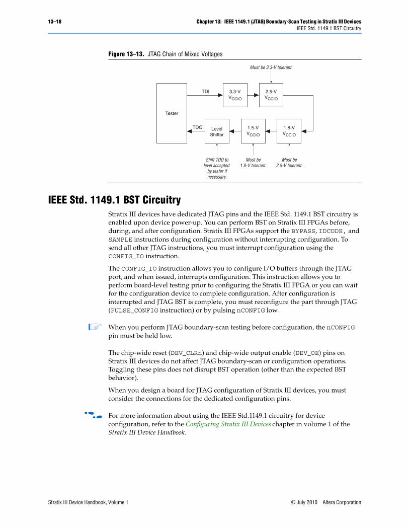
You can interface the TDI and TDO lines of the devices that have different VCCIO levels by inserting a level shifter between the devices. If possible, you should build the JTAG chain in such a way that a device with a higher VCCIO level drives to a device with an equal or lower VCCIO level. This way, a level shifter is used only to shift the TDO level to a level acceptable to the JTAG tester. Figure 13–13 shows the JTAG chain of mixed voltages and how a level shifter is inserted in the chain.
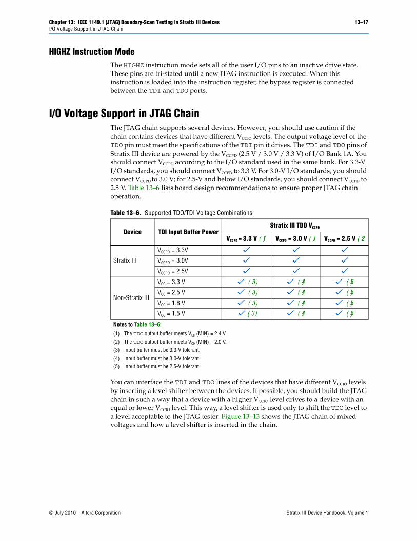
Table 13–6. Supported TDO/TDI Voltage Combinations
Device TDI Input Buffer PowerStratix III TDO VCCPD
VCCPD = 3.3 V (1) VCCPD = 3.0 V (1) VCCPD = 2.5 V (2)
Stratix III
VCCPD = 3.3V v v v
VCCPD = 3.0V v v v
VCCPD = 2.5V v v v
Non-Stratix III
VCC = 3.3 V v (3) v (4) v (5)
VCC = 2.5 V v (3) v (4) v (5)
VCC = 1.8 V v (3) v (4) v (5)
VCC = 1.5 V v (3) v (4) v (5)
Notes to Table 13–6:
(1) The TDO output buffer meets VOH (MIN) = 2.4 V.(2) The TDO output buffer meets VOH (MIN) = 2.0 V.(3) Input buffer must be 3.3-V tolerant.(4) Input buffer must be 3.0-V tolerant.(5) Input buffer must be 2.5-V tolerant.
© July 2010 Altera Corporation Stratix III Device Handbook, Volume 1
13–18 Chapter 13: IEEE 1149.1 (JTAG) Boundary-Scan Testing in Stratix III DevicesIEEE Std. 1149.1 BST Circuitry
IEEE Std. 1149.1 BST Circuitry Stratix III devices have dedicated JTAG pins and the IEEE Std. 1149.1 BST circuitry is enabled upon device power-up. You can perform BST on Stratix III FPGAs before, during, and after configuration. Stratix III FPGAs support the BYPASS, IDCODE, and SAMPLE instructions during configuration without interrupting configuration. To send all other JTAG instructions, you must interrupt configuration using the CONFIG_IO instruction.
The CONFIG_IO instruction allows you to configure I/O buffers through the JTAG port, and when issued, interrupts configuration. This instruction allows you to perform board-level testing prior to configuring the Stratix III FPGA or you can wait for the configuration device to complete configuration. After configuration is interrupted and JTAG BST is complete, you must reconfigure the part through JTAG (PULSE_CONFIG instruction) or by pulsing nCONFIG low.
1 When you perform JTAG boundary-scan testing before configuration, the nCONFIG pin must be held low.
The chip-wide reset (DEV_CLRn) and chip-wide output enable (DEV_OE) pins on Stratix III devices do not affect JTAG boundary-scan or configuration operations. Toggling these pins does not disrupt BST operation (other than the expected BST behavior).
When you design a board for JTAG configuration of Stratix III devices, you must consider the connections for the dedicated configuration pins.
f For more information about using the IEEE Std.1149.1 circuitry for device configuration, refer to the Configuring Stratix III Devices chapter in volume 1 of the Stratix III Device Handbook.
Figure 13–13. JTAG Chain of Mixed Voltages
3.3-VVCCIO
LevelShifter
2.5-VVCCIO
1.8-VVCCIO
1.5-VVCCIO
Tester
TDO
TDI
Must be 3.3-V tolerant.
Shift TDO tolevel accepted
by tester ifnecessary.
Must be1.8-V tolerant.
Must be2.5-V tolerant.
Stratix III Device Handbook, Volume 1 © July 2010 Altera Corporation
Chapter 13: IEEE 1149.1 (JTAG) Boundary-Scan Testing in Stratix III Devices 13–19IEEE Std. 1149.1 BST Circuitry (Disabling)
IEEE Std. 1149.1 BST Circuitry (Disabling)The IEEE Std. 1149.1 BST circuitry for Stratix III devices is enabled upon device power-up. Because the IEEE Std. 1149.1 BST circuitry is used for BST or in-circuit reconfiguration, you must enable the circuitry only at specific times as mentioned in, “IEEE Std. 1149.1 BST Circuitry” on page 13–18.
1 If you are not using the IEEE Std. 1149.1 circuitry in Stratix III, you should permanently disable the circuitry to ensure that you do not inadvertently enable it when it is not required.
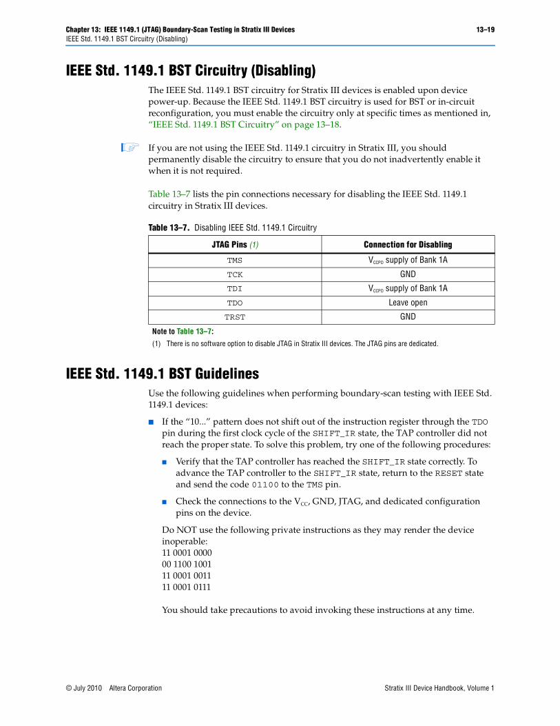
Table 13–7 lists the pin connections necessary for disabling the IEEE Std. 1149.1 circuitry in Stratix III devices.
IEEE Std. 1149.1 BST GuidelinesUse the following guidelines when performing boundary-scan testing with IEEE Std. 1149.1 devices:
■ If the “10...” pattern does not shift out of the instruction register through the TDO pin during the first clock cycle of the SHIFT_IR state, the TAP controller did not reach the proper state. To solve this problem, try one of the following procedures:
■ Verify that the TAP controller has reached the SHIFT_IR state correctly. To advance the TAP controller to the SHIFT_IR state, return to the RESET state and send the code 01100 to the TMS pin.
■ Check the connections to the VCC, GND, JTAG, and dedicated configuration pins on the device.
Do NOT use the following private instructions as they may render the device inoperable: 11 0001 000000 1100 100111 0001 001111 0001 0111
You should take precautions to avoid invoking these instructions at any time.
Table 13–7. Disabling IEEE Std. 1149.1 Circuitry
JTAG Pins (1) Connection for Disabling
TMS VCCPD supply of Bank 1A
TCK GND
TDI VCCPD supply of Bank 1A
TDO Leave open
TRST GND
Note to Table 13–7:
(1) There is no software option to disable JTAG in Stratix III devices. The JTAG pins are dedicated.
© July 2010 Altera Corporation Stratix III Device Handbook, Volume 1
13–20 Chapter 13: IEEE 1149.1 (JTAG) Boundary-Scan Testing in Stratix III DevicesBoundary-Scan Description Language (BSDL) Support
■ Perform a SAMPLE/PRELOAD test cycle prior to the first EXTEST test cycle to ensure that known data is present at the device pins when you enter the EXTEST mode. If the OEJ update register contains a 0, the data in the OUTJ update register is driven out. The state must be known and correct to avoid contention with other devices in the system.
■ Do not perform EXTEST testing during ICR. This instruction is supported before or after ICR, but not during ICR. Use the CONFIG_IO instruction to interrupt configuration and then perform testing, or wait for configuration to complete.
■ If performing testing before configuration, hold the nCONFIG pin low.
f For more information about boundary scan testing, contact Altera® Application at www.altera.com.
Boundary-Scan Description Language (BSDL) Support The Boundary-Scan Description Language (BSDL), a subset of VHDL, provides a syntax that allows you to describe the features of an IEEE Std. 1149.1 BST-capable device that can be tested. Test software development systems then use the BSDL files for test generation, analysis, and failure diagnostics.
f For more information about BSDL files for IEEE Std. 1149.1-compliant Stratix III devices, refer to the Stratix III BSDL Files page on the Altera website.
To perform BST on a configured device, you will require a post configuration BSDL file that is customized to your design. This file can be generated with the BSDL Customizer script.
f For more information about the BSDL Customizer, refer to the Altera BSDL Support page on the Altera website.
Stratix III Device Handbook, Volume 1 © July 2010 Altera Corporation
Chapter 13: IEEE 1149.1 (JTAG) Boundary-Scan Testing in Stratix III Devices 13–21Chapter Revision History
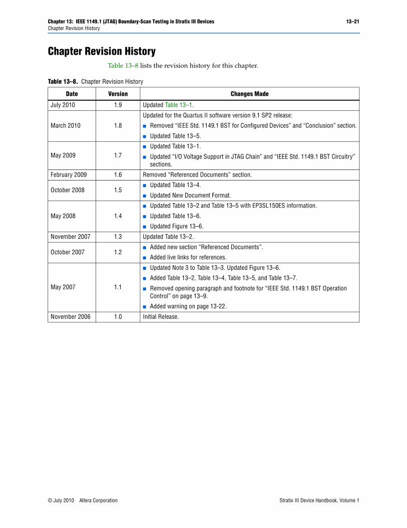
Chapter Revision HistoryTable 13–8 lists the revision history for this chapter.
Table 13–8. Chapter Revision History
Date Version Changes Made
July 2010 1.9 Updated Table 13–1.
March 2010 1.8
Updated for the Quartus II software version 9.1 SP2 release:
■ Removed “IEEE Std. 1149.1 BST for Configured Devices” and “Conclusion” section.
■ Updated Table 13–5.
May 2009 1.7■ Updated Table 13–1.
■ Updated “I/O Voltage Support in JTAG Chain” and “IEEE Std. 1149.1 BST Circuitry” sections.
February 2009 1.6 Removed “Referenced Documents” section.
October 2008 1.5■ Updated Table 13–4.
■ Updated New Document Format.
May 2008 1.4
■ Updated Table 13–2 and Table 13–5 with EP3SL150ES information.
■ Updated Table 13–6.
■ Updated Figure 13–6.
November 2007 1.3 Updated Table 13–2.
October 2007 1.2■ Added new section “Referenced Documents”.
■ Added live links for references.
May 2007 1.1
■ Updated Note 3 to Table 13–3. Updated Figure 13–6.
■ Added Table 13–2, Table 13–4, Table 13–5, and Table 13–7.
■ Removed opening paragraph and footnote for “IEEE Std. 1149.1 BST Operation Control” on page 13–9.
■ Added warning on page 13-22.
November 2006 1.0 Initial Release.
© July 2010 Altera Corporation Stratix III Device Handbook, Volume 1

13–22 Chapter 13: IEEE 1149.1 (JTAG) Boundary-Scan Testing in Stratix III DevicesChapter Revision History
Stratix III Device Handbook, Volume 1 © July 2010 Altera Corporation