Embed Size (px)
Citation preview
IEEE TRANSACTIONS ON ADVANCED PACKAGING, VOL. ??, NO. ??, MONTH ??, 2011 1
Fast and Accurate Analytical Modeling ofThrough-Silicon-Via Capacitive Coupling
Dae Hyun Kim, Student Member, IEEE, Saibal Mukhopadhyay, Member, IEEE, and Sung Kyu Lim, SeniorMember, IEEE
Abstract— In this paper, we present analytical models for fastestimation of coupling capacitance of square-shaped TSVs in 3DICs. Errors between our model and Synopsys Raphael simulationon regular TSV structures remain less than 6.03% while thecomputation time of our model for capacitance estimation is neg-ligible. We also develop a simple capacitance estimation techniqueto extract TSV-to-TSV coupling capacitance in general layouts.Average errors between our model and Raphael simulation onrandom TSV structures is 5.06% to 8.24%, and maximum errorsremain less than 18.91% which is tolerable for fast capacitanceestimation in CAD area.
Index Terms— 3D IC, Through-silicon via (TSV), capacitance,timing analysis
I. INTRODUCTION
DRIVEN by the need for performance improvement, alarge number of universities and companies are actively
researching 3D IC, which is expected to lead to shortertotal wirelength, higher clock frequency, and lower powerconsumption than 2D IC [1]–[3]. In 3D IC, multiple diesare stacked, and vertical interconnections between dies arerealized by through-silicon vias (TSVs). These TSVs play acentral role in replacing long interconnects found in 2D ICswith short vertical interconnects. Shortened wires will resultin low wire delay, thereby improving performance. In additionto performance improvement, it is also possible with 3Dheterogeneous integration to stack disparate technologies toprovide a 3D structure with heterogeneous functions includinglogic, memory, MEMS, antennas, display, RF, analog/digital,sensors, and power conversion and storage. Therefore uni-versities and companies have been actively developing TSVmanufacturing and die-to-die bonding technologies [4]–[9].Moreover, various works on utilizing TSVs for physical designhave also been proposed recently [10], [11].
The basic electrical characteristics of TSVs such as resis-tance, capacitance, and inductance have also been investigatedin the literature to provide circuit designers with physicalanalysis and ranges of their values [12]–[16]. One of the resultsto notice is that TSV coupling capacitance is very big (tensof femto-farads) [13] so that it has huge impact on timing
The authors are with the School of Electrical and Computer Engineering,Georgia Institute of Technology.
This research is based upon the work supported by the National ScienceFoundation under CAREER Grant No. CCF-0546382 and CCF-0917000; theSRC Interconnect Focus Center (IFC), and Intel Corporation.
Copyright (c) 200? IEEE. Personal use of this material is permitted.However, permission to use this material for any other purposes must beobtained from the IEEE by sending an email to [email protected].
Publisher Item Identifier ???.
and interconnect power [17], [18]. Therefore, computer-aideddesign (CAD) tools are required to compute TSV couplingcapacitance quickly but accurately during placement, routing,and optimization of timing and power in 3D ICs.
TSV-to-TSV (or TSV-to-wire) coupling capacitance is af-fected by TSV-to-TSV (or TSV-to-wire) distance, TSV andwire dimensions, the number of surrounding TSVs and wires,and their spatial distribution. It is therefore almost impossibleto use look-up tables to compute TSV capacitance quicklybecause too many variables exist. In addition, it is alsoalmost impossible to use field solvers for TSV capacitancecomputation during placement, routing, or optimization oftiming and power because field solvers require non-negligibleamount of computation time.
In this paper, we present an accurate analytical model for thecoupling capacitance among square-shaped TSVs and wires.In order to model layouts accurately, we consider various typesof coupling and fringe capacitances while taking neighboringTSVs and wires into account. Our experiments show thaterrors between our model and Synopsys Raphael simulationremain less than 6.03% on regular TSV structures, and averageerrors on random TSV structures remain less than 5.06% to8.24% while our model requires a fraction of runtime forcapacitance computation.
This paper is organized as follows. In Section II, we brieflydiscuss device structures in 3D ICs and review TSV couplingmodels. Section III shows basic formulas for capacitancecomputation. In Section IV and Section V, we present our ana-lytical models for fast estimation of TSV coupling capacitance.Capacitance estimation results on regular TSV structures andthe impact of TSV capacitance on signal delay are presentedin Section VI. We compare capacitances obtained from ourmodel and Raphael simulation on random TSV structures inSection VII, and conclude in Section VIII.
II. DEVICE STRUCTURE
A. TSV Formation and Die Bonding
Fig. 1 shows three types of die bonding and two typesof TSVs. Under the via-first technology, devices and TSVsare fabricated first, metal layers are deposited, and thendies are bonded. Therefore, TSVs in via-first technology aresurrounded by other TSVs laterally and by wires vertically.In via-last technology, on the other hand, devices and metallayers are fabricated first, TSVs are fabricated through all thelayers from the substrate to the topmost metal layer, and thendies are bonded. Therefore, TSVs in via-last technology are
IEEE TRANSACTIONS ON ADVANCED PACKAGING, VOL. ??, NO. ??, MONTH ??, 2011 2
(a) face-to-face (b) face-to-back (a) back-to-back
Fig. 1. Three types of die bonding (face-to-face, face-to-back, and back-to-back) and two types of TSVs (via-first and via-last).
M3
M2
M1
substrate
Mtop
bonding layer
Mtop-1
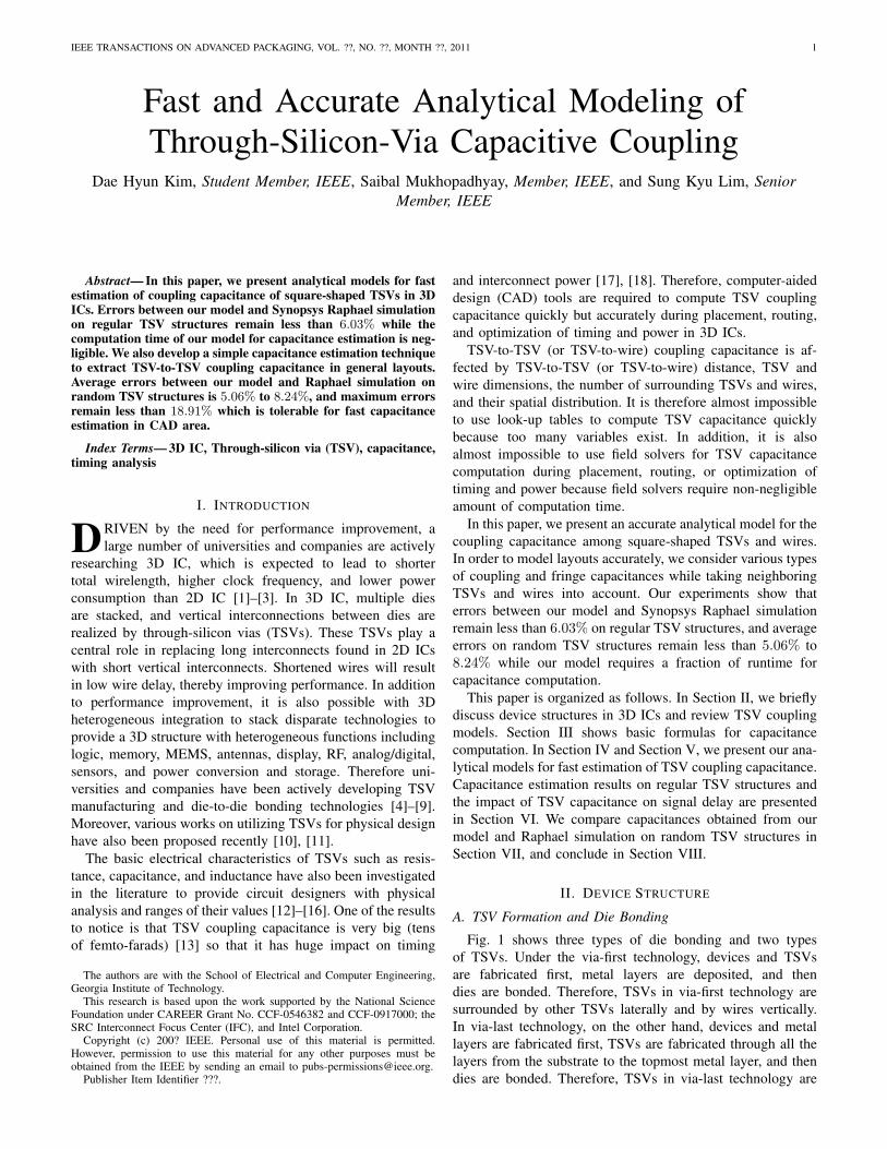
Fig. 2. Capacitive coupling in via-first TSV technology.
M3
M2
M1
substrate
Mtop
bonding layer
Mtop-1
Fig. 3. Capacitive coupling in via-last TSV technology.
surrounded by other TSVs laterally and by wires laterally andvertically.
B. TSV Coupling Capacitance
TSV coupling capacitance consists mainly of two compo-nents as follows:
• Capacitive coupling (CTW in Fig. 2 and Fig. 3) betweena TSV and wires surrounding the TSV. These wires existon the top or bottom of TSVs in via-first case as shownin Fig. 2. In case of via-last TSVs, there exists capacitivecoupling between a TSV and neighboring wires in metallayers as shown in Fig. 3.
• Capacitive coupling (CTT in Fig. 2 and Fig. 3) betweentwo TSVs.
To analyze physical phenomena between two TSVs inthe substrate, we review previous models presented in the
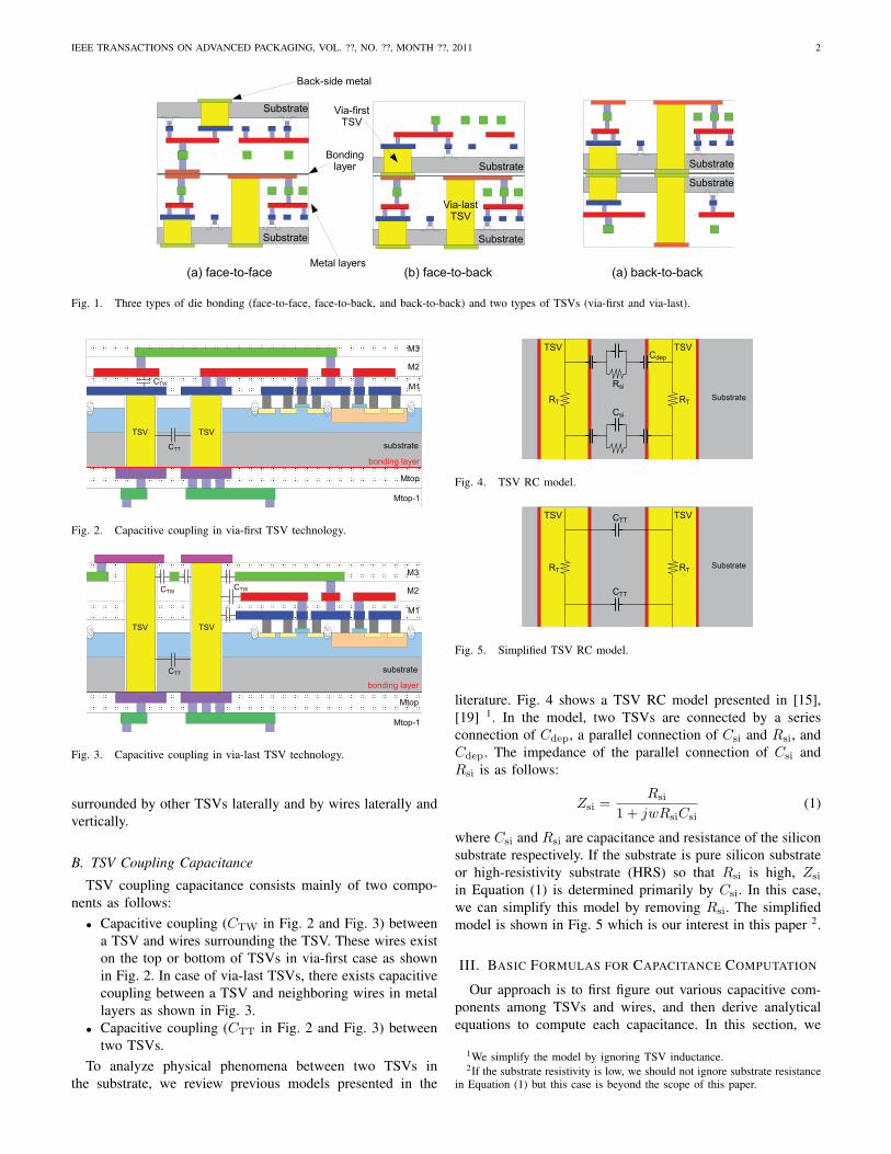
Fig. 4. TSV RC model.
Fig. 5. Simplified TSV RC model.
literature. Fig. 4 shows a TSV RC model presented in [15],[19] 1. In the model, two TSVs are connected by a seriesconnection of Cdep, a parallel connection of Csi and Rsi, andCdep. The impedance of the parallel connection of Csi andRsi is as follows:
Zsi =Rsi
1 + jwRsiCsi(1)
where Csi and Rsi are capacitance and resistance of the siliconsubstrate respectively. If the substrate is pure silicon substrateor high-resistivity substrate (HRS) so that Rsi is high, Zsi
in Equation (1) is determined primarily by Csi. In this case,we can simplify this model by removing Rsi. The simplifiedmodel is shown in Fig. 5 which is our interest in this paper 2.
III. BASIC FORMULAS FOR CAPACITANCE COMPUTATION
Our approach is to first figure out various capacitive com-ponents among TSVs and wires, and then derive analyticalequations to compute each capacitance. In this section, we
1We simplify the model by ignoring TSV inductance.2If the substrate resistivity is low, we should not ignore substrate resistance
in Equation (1) but this case is beyond the scope of this paper.
IEEE TRANSACTIONS ON ADVANCED PACKAGING, VOL. ??, NO. ??, MONTH ??, 2011 3
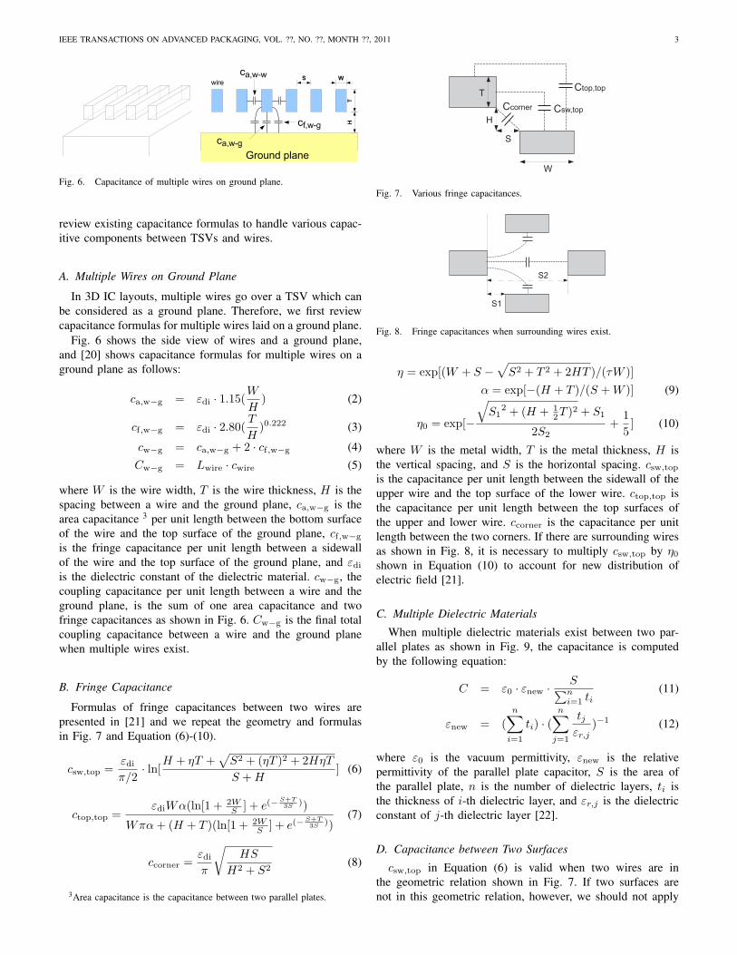
Fig. 6. Capacitance of multiple wires on ground plane.
review existing capacitance formulas to handle various capac-itive components between TSVs and wires.
A. Multiple Wires on Ground Plane
In 3D IC layouts, multiple wires go over a TSV which canbe considered as a ground plane. Therefore, we first reviewcapacitance formulas for multiple wires laid on a ground plane.
Fig. 6 shows the side view of wires and a ground plane,and [20] shows capacitance formulas for multiple wires on aground plane as follows:
ca,w−g = εdi · 1.15(W
H) (2)
cf,w−g = εdi · 2.80(T
H)0.222 (3)
cw−g = ca,w−g + 2 · cf,w−g (4)Cw−g = Lwire · cwire (5)
where W is the wire width, T is the wire thickness, H is thespacing between a wire and the ground plane, ca,w−g is thearea capacitance 3 per unit length between the bottom surfaceof the wire and the top surface of the ground plane, cf,w−g
is the fringe capacitance per unit length between a sidewallof the wire and the top surface of the ground plane, and εdiis the dielectric constant of the dielectric material. cw−g, thecoupling capacitance per unit length between a wire and theground plane, is the sum of one area capacitance and twofringe capacitances as shown in Fig. 6. Cw−g is the final totalcoupling capacitance between a wire and the ground planewhen multiple wires exist.
B. Fringe Capacitance
Formulas of fringe capacitances between two wires arepresented in [21] and we repeat the geometry and formulasin Fig. 7 and Equation (6)-(10).
csw,top =εdiπ/2
· ln[H + ηT +
√S2 + (ηT )2 + 2HηT
S +H] (6)
ctop,top =εdiWα(ln[1 + 2W
S ] + e(−S+T3S ))
Wπα+ (H + T )(ln[1 + 2WS ] + e(−
S+T3S ))
(7)
ccorner =εdiπ
√HS
H2 + S2(8)
3Area capacitance is the capacitance between two parallel plates.
Ctop,top
Csw,top
W
T
Ccorner
S
H
Fig. 7. Various fringe capacitances.
S1
S2
Fig. 8. Fringe capacitances when surrounding wires exist.
η = exp[(W + S −√S2 + T 2 + 2HT )/(τW )]
α = exp[−(H + T )/(S +W )] (9)
η0 = exp[−
√S1
2 + (H + 12T )
2 + S1
2S2+
1
5] (10)
where W is the metal width, T is the metal thickness, H isthe vertical spacing, and S is the horizontal spacing. csw,top
is the capacitance per unit length between the sidewall of theupper wire and the top surface of the lower wire. ctop,top isthe capacitance per unit length between the top surfaces ofthe upper and lower wire. ccorner is the capacitance per unitlength between the two corners. If there are surrounding wiresas shown in Fig. 8, it is necessary to multiply csw,top by η0shown in Equation (10) to account for new distribution ofelectric field [21].
C. Multiple Dielectric Materials
When multiple dielectric materials exist between two par-allel plates as shown in Fig. 9, the capacitance is computedby the following equation:
C = ε0 · εnew · S∑ni=1 ti
(11)
εnew = (n∑
i=1
ti) · (n∑
j=1
tjεr,j
)−1 (12)
where ε0 is the vacuum permittivity, εnew is the relativepermittivity of the parallel plate capacitor, S is the area ofthe parallel plate, n is the number of dielectric layers, ti isthe thickness of i-th dielectric layer, and εr,j is the dielectricconstant of j-th dielectric layer [22].
D. Capacitance between Two Surfaces
csw,top in Equation (6) is valid when two wires are inthe geometric relation shown in Fig. 7. If two surfaces arenot in this geometric relation, however, we should not apply
IEEE TRANSACTIONS ON ADVANCED PACKAGING, VOL. ??, NO. ??, MONTH ??, 2011 4
Fig. 9. Multiple dielectric materials in a parallel plate capacitor.
Fig. 10. Capacitance between two surfaces.
csw,top directly to compute the coupling capacitance of thetwo surfaces. Fig. 10 shows an example where the geometricrelation between the two surfaces F1 and F2 is different fromthe geometric relation in Fig. 7.
In this case, we use a simple approximation technique asfollows. First, we find a flat equipotential plane between thetwo metal surfaces. Then we compute the coupling capacitancebetween a metal surface and the equipotential plane (Ct1 andCt2 in the figure). Finally the coupling capacitance betweenthe two metal surfaces is computed by the series connectionof the two coupling capacitances. In Fig. 10, for example,we compute the coupling capacitance between two metalsurfaces F1 and F2 by assuming the equipotential plane Peq
and computing Ct1 and Ct2 using csw,top. The final couplingcapacitance between F1 and F2 is the capacitance of the seriesconnection of Ct1 and Ct2.
We generate several geometries, apply this technique, andcompare results against Raphael simulation in order to validatethis approximation technique. The error is around 10% butthis is tolerable because absolute values of this kind of fringecapacitance are much smaller than TSV-to-TSV couplingcapacitance or TSV-to-wire area capacitance.
IV. TSVS WITH TOP AND BOTTOM NEIGHBORS
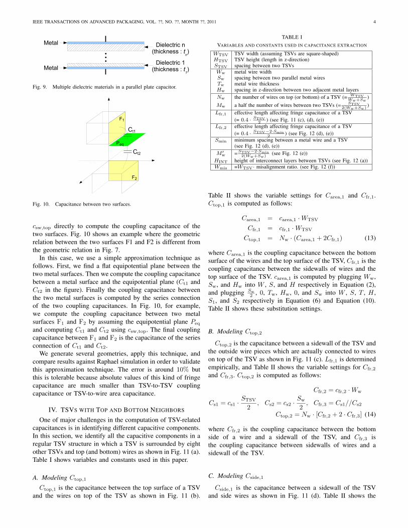
One of major challenges in the computation of TSV-relatedcapacitances is in identifying different capacitive components.In this section, we identify all the capacitive components in aregular TSV structure in which a TSV is surrounded by eightother TSVs and top (and bottom) wires as shown in Fig. 11 (a).Table I shows variables and constants used in this paper.
A. Modeling Ctop,1
Ctop,1 is the capacitance between the top surface of a TSVand the wires on top of the TSV as shown in Fig. 11 (b).
TABLE IVARIABLES AND CONSTANTS USED IN CAPACITANCE EXTRACTION
WTSV TSV width (assuming TSVs are square-shaped)HTSV TSV height (length in z-direction)STSV spacing between two TSVsWw metal wire widthSw spacing between two parallel metal wiresTw metal wire thicknessHw spacing in z-direction between two adjacent metal layersNw the number of wires on top (or bottom) of a TSV (= WTSV
Ww+Sw)
Mw a half the number of wires between two TSVs (= STSV2(Ww+Sw)
)Lfr,1 effective length affecting fringe capacitance of a TSV
(= 0.4 · STSV2
) (see Fig. 11 (c), (d), (e))Lfr,2 effective length affecting fringe capacitance of a TSV
(= 0.4 · STSV−2·Smin2
) (see Fig. 12 (d), (e))Smin minimum spacing between a metal wire and a TSV
(see Fig. 12 (d), (e))M ′
w =STSV−2·Smin2(Ww+Sw)
(see Fig. 12 (e))HINT height of interconnect layers between TSVs (see Fig. 12 (a))Wmis =WTSV· misalignment ratio. (see Fig. 12 (f))
Table II shows the variable settings for Carea,1 and Cfr,1.Ctop,1 is computed as follows:
Carea,1 = carea,1 ·WTSV
Cfr,1 = cfr,1 ·WTSV
Ctop,1 = Nw · (Carea,1 + 2Cfr,1) (13)
where Carea,1 is the coupling capacitance between the bottomsurface of the wires and the top surface of the TSV, Cfr,1 is thecoupling capacitance between the sidewalls of wires and thetop surface of the TSV. carea,1 is computed by plugging Ww,Sw, and Hw into W , S, and H respectively in Equation (2),and plugging Sw
2 , 0, Tw, Hw, 0, and Sw into W , S, T , H ,S1, and S2 respectively in Equation (6) and Equation (10).Table II shows these substitution settings.
B. Modeling Ctop,2
Ctop,2 is the capacitance between a sidewall of the TSV andthe outside wire pieces which are actually connected to wireson top of the TSV as shown in Fig. 11 (c). Lfr,1 is determinedempirically, and Table II shows the variable settings for Cfr,2
and Cfr,3. Ctop,2 is computed as follows:
Cfr,2 = cfr,2 ·Ww
Cs1 = cs1 ·STSV
2, Cs2 = cs2 ·
Sw
2, Cfr,3 = Cs1//Cs2
Ctop,2 = Nw · [Cfr,2 + 2 · Cfr,3] (14)
where Cfr,2 is the coupling capacitance between the bottomside of a wire and a sidewall of the TSV, and Cfr,3 isthe coupling capacitance between sidewalls of wires and asidewall of the TSV.
C. Modeling Cside,1
Cside,1 is the capacitance between a sidewall of the TSVand side wires as shown in Fig. 11 (d). Table II shows the
IEEE TRANSACTIONS ON ADVANCED PACKAGING, VOL. ??, NO. ??, MONTH ??, 2011 5
(a) capacitive components with top and/or bottom wires (b) capacitive components of Ctop,1 (c) capacitive components of Ctop,2
(d) capacitive components of Cside,1 (e) capacitive components of Cside,2 (f) capacitive components of Ccoupling
Fig. 11. Capacitive components of TSVs with top and bottom neighboring wires
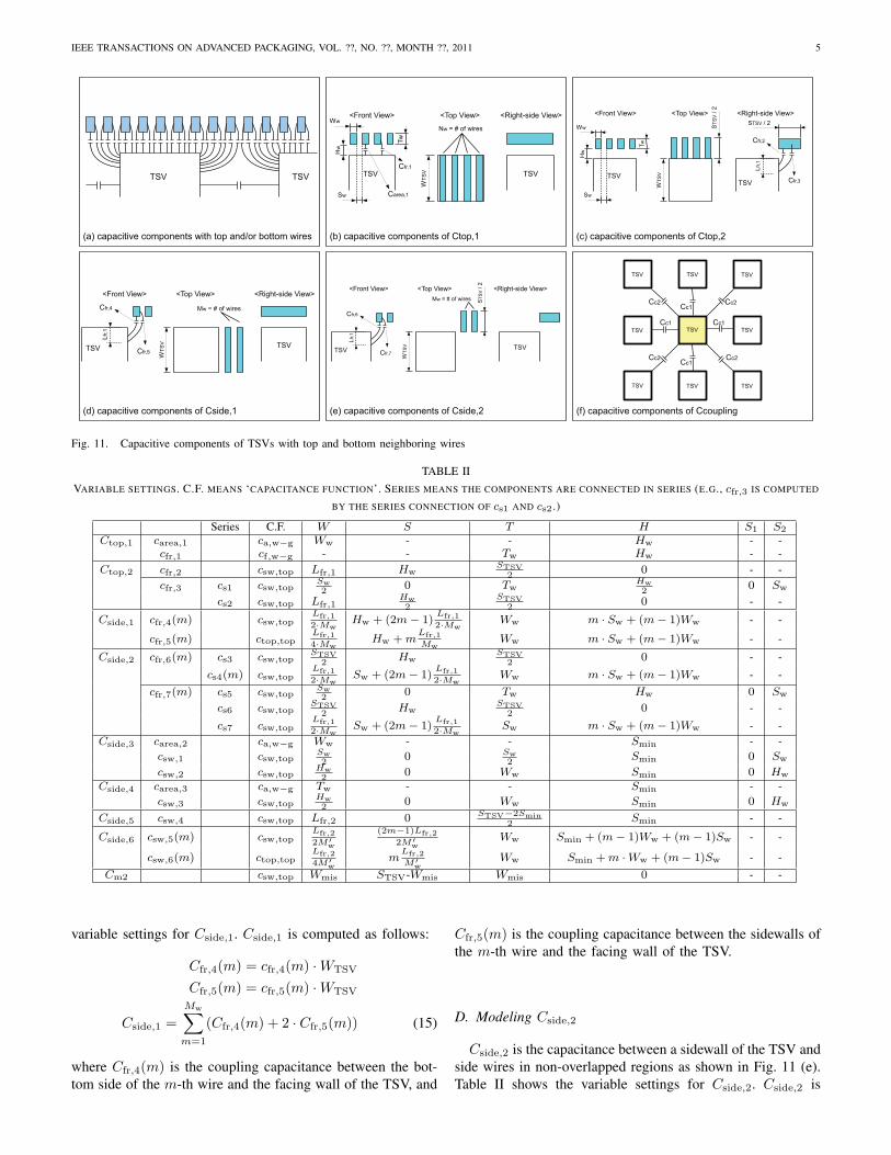
TABLE IIVARIABLE SETTINGS. C.F. MEANS ‘CAPACITANCE FUNCTION’. SERIES MEANS THE COMPONENTS ARE CONNECTED IN SERIES (E.G., cfr,3 IS COMPUTED
BY THE SERIES CONNECTION OF cs1 AND cs2 .)
Series C.F. W S T H S1 S2
Ctop,1 carea,1 ca,w−g Ww - - Hw - -cfr,1 cf,w−g - - Tw Hw - -
Ctop,2 cfr,2 csw,top Lfr,1 HwSTSV
20 - -
cfr,3 cs1 csw,topSw2
0 TwHw2
0 Sw
cs2 csw,top Lfr,1Hw2
STSV2
0 - -
Cside,1 cfr,4(m) csw,topLfr,1
2·MwHw + (2m− 1)
Lfr,1
2·MwWw m · Sw + (m− 1)Ww - -
cfr,5(m) ctop,topLfr,1
4·MwHw +m
Lfr,1
MwWw m · Sw + (m− 1)Ww - -
Cside,2 cfr,6(m) cs3 csw,topSTSV
2Hw
STSV2
0 - -
cs4(m) csw,topLfr,1
2·MwSw + (2m− 1)
Lfr,1
2·MwWw m · Sw + (m− 1)Ww - -
cfr,7(m) cs5 csw,topSw2
0 Tw Hw 0 Sw
cs6 csw,topSTSV
2Hw
STSV2
0 - -
cs7 csw,topLfr,1
2·MwSw + (2m− 1)
Lfr,1
2·MwSw m · Sw + (m− 1)Ww - -
Cside,3 carea,2 ca,w−g Ww - - Smin - -csw,1 csw,top
Sw2
0 Sw2
Smin 0 Sw
csw,2 csw,topHw2
0 Ww Smin 0 Hw
Cside,4 carea,3 ca,w−g Tw - - Smin - -csw,3 csw,top
Hw2
0 Ww Smin 0 Hw
Cside,5 csw,4 csw,top Lfr,2 0 STSV−2Smin2
Smin - -
Cside,6 csw,5(m) csw,topLfr,2
2M′w
(2m−1)Lfr,2
2M′w
Ww Smin + (m− 1)Ww + (m− 1)Sw - -
csw,6(m) ctop,topLfr,2
4M′w
mLfr,2
M′w
Ww Smin +m ·Ww + (m− 1)Sw - -Cm2 csw,top Wmis STSV-Wmis Wmis 0 - -
variable settings for Cside,1. Cside,1 is computed as follows:
Cfr,4(m) = cfr,4(m) ·WTSV
Cfr,5(m) = cfr,5(m) ·WTSV
Cside,1 =
Mw∑m=1
(Cfr,4(m) + 2 · Cfr,5(m)) (15)
where Cfr,4(m) is the coupling capacitance between the bot-tom side of the m-th wire and the facing wall of the TSV, and
Cfr,5(m) is the coupling capacitance between the sidewalls ofthe m-th wire and the facing wall of the TSV.
D. Modeling Cside,2
Cside,2 is the capacitance between a sidewall of the TSV andside wires in non-overlapped regions as shown in Fig. 11 (e).Table II shows the variable settings for Cside,2. Cside,2 is
IEEE TRANSACTIONS ON ADVANCED PACKAGING, VOL. ??, NO. ??, MONTH ??, 2011 6
computed as follows:
Cs3 = cs3 ·Ww, Cs4(m) = cs4(m) · STSV
2Cfr,6(m) = Cs3//Cs4(m)
Cs5 = cs5 ·STSV
2, Cs6 = cs6 · Sw
Cs7(m) = cs7(m) · STSV
2Cfr,7(m) = Cs5//Cs6//Cs7(m)
Cside,2 =
Mw∑m=1
[Cfr,6(m) + 2 · Cfr,7(m)] (16)
where Cfr,6(m) is the coupling capacitance between the bot-tom side of the m-th wire and the facing sidewall of the TSV,and Cfr,7(m) is the coupling capacitance between sidewalls ofthe m-th wire and the facing sidewall of the TSV.
E. Modeling CTT
As mentioned in Section II, there exists capacitive couplingbetween two adjacent TSVs. This coupling capacitance CTT
between two TSVs consists of two components. The firstcomponent is the coupling capacitance (Cc1 in Fig. 11 (f))between the sidewalls of the TSVs, and the second componentis the coupling capacitance (Cc2 in Fig. 11 (f)) between thecorners of the TSVs. Cc1 is computed as follows:
Cc1 = εdi(HTSV − 2 · Lfr,1) ·WTSV
STSV(17)
ccorner in Equation (8) which will be used for the computationof Cc2 is dependent on S/H . If H and S are constants,ccorner also becomes a constant. In our case, however, thewidth, height, and spacing of TSVs vary in a wide range.Therefore, we find a proportional constant Kcorner empiricallyand compute Cc2 as follows:
Cc2 =εdi
π√2·HTSV ·Kcorner (18)
Kcorner =1
2· HTSV
STSV(if
HTSV
STSV≤ 4.0)
= 2.0 (ifHTSV
STSV≥ 4.0) (19)
Lastly, CTT is computed by the following equation:
CTT = 4(Cc1 + Cc2) (20)
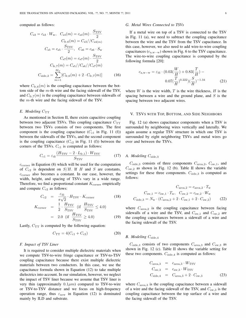
F. Impact of TSV Liner
It is required to consider multiple dielectric materials whenwe compute TSV-to-wire fringe capacitance or TSV-to-TSVcoupling capacitance because there exist multiple dielectricmaterials between two conductors. In this case, we use thecapacitance formula shown in Equation (12) to take multipledielectrics into account. In our simulation, however, we neglectthe impact of TSV liner because we assume that TSV liner isvery thin (approximately 0.1µm) compared to TSV-to-wireor TSV-to-TSV distance and we focus on high-frequencyoperation range, thus εnew in Equation (12) is dominatedmainly by ILD and substrate.
G. Metal Wires Connected to TSVs
If a metal wire on top of a TSV is connected to the TSVin Fig. 11 (a), we need to subtract the coupling capacitancebetween the wire and the TSV from the TSV capacitance. Inthis case, however, we also need to add wire-to-wire couplingcapacitances (ca,w−w) shown in Fig. 6 to the TSV capacitance.The wire-to-wire coupling capacitance is computed by thefollowing formula [20]:
ca,w−w = εdi · (0.03(W
H) + 0.83(
T
H)−
0.07(T
H)0.222)(
S
H)−1.34 (21)
where W is the wire width, T is the wire thickness, H is thespacing between a wire and the ground plane, and S is thespacing between two adjacent wires.
V. TSVS WITH TOP, BOTTOM, AND SIDE NEIGHBORS
Fig. 12 (a) shows capacitance components when a TSV issurrounded by neighboring wires vertically and laterally. Weagain assume a regular TSV structure in which one TSV issurrounded by eight neighboring TSVs and metal wires goover and between the TSVs.
A. Modeling Cside,3
Cside,3 consists of three components Carea,2, Csw,1, andCsw,2 as shown in Fig. 12 (b). Table II shows the variablesettings for these three components. Cside,3 is computed asfollows:
Carea,2 = carea,2 · Tw
Csw,1 = csw,1 · Tw, Csw,2 = csw,2 ·Ww
Cside,3 = Nw · (Carea,2 + 2 · Csw,1 + 2 · Csw,2) (22)
where Carea,2 is the coupling capacitance between facingsidewalls of a wire and the TSV, and Csw,1 and Csw,2 arethe coupling capacitances between a sidewall of a wire andthe facing sidewall of the TSV.
B. Modeling Cside,4
Cside,4 consists of two components Carea,3 and Csw,3 asshown in Fig. 12 (c). Table II shows the variable setting forthese two components. Cside,4 is computed as follows:
Carea,3 = carea,3 ·WTSV
Csw,3 = csw,3 ·WTSV
Cside,4 = Carea,3 + 2 · Csw,3 (23)
where Carea,3 is the coupling capacitance between a sidewallof a wire and the facing sidewall of the TSV, and Csw,3 is thecoupling capacitance between the top surface of a wire andthe facing sidewall of the TSV.
IEEE TRANSACTIONS ON ADVANCED PACKAGING, VOL. ??, NO. ??, MONTH ??, 2011 7
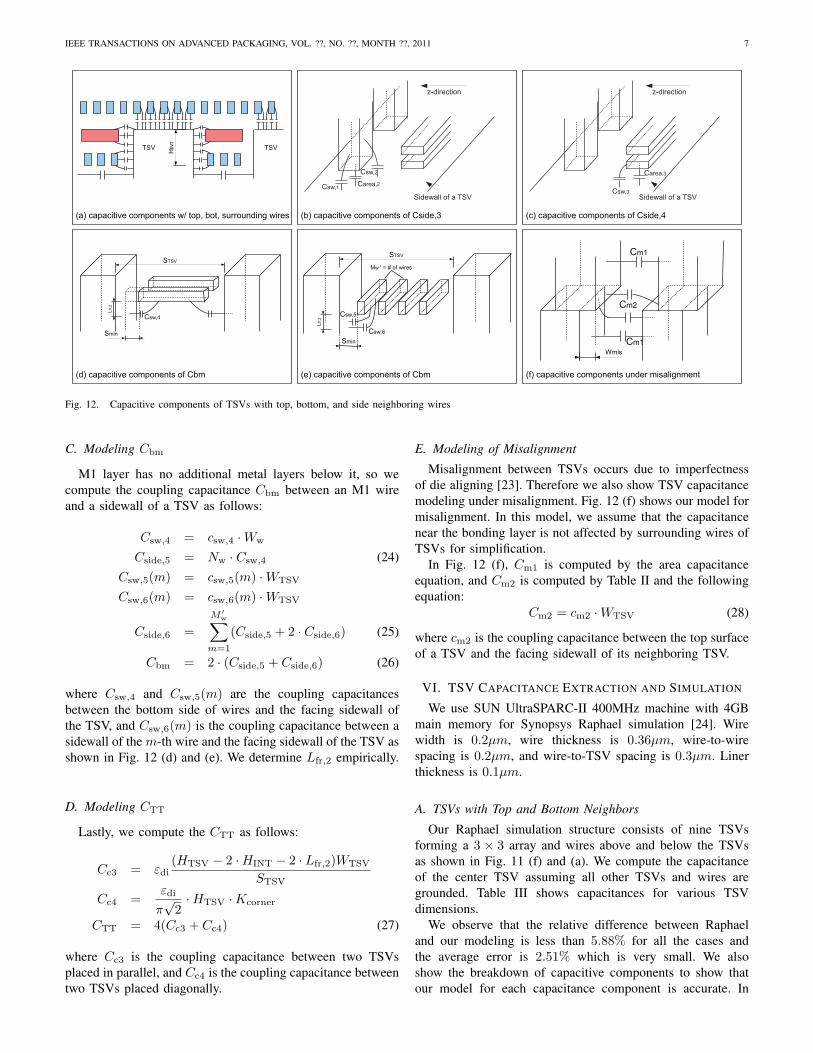
(a) capacitive components w/ top, bot, surrounding wires (b) capacitive components of Cside,3
(d) capacitive components of Cbm (e) capacitive components of Cbm (f) capacitive components under misalignment
(c) capacitive components of Cside,4
Fig. 12. Capacitive components of TSVs with top, bottom, and side neighboring wires
C. Modeling Cbm
M1 layer has no additional metal layers below it, so wecompute the coupling capacitance Cbm between an M1 wireand a sidewall of a TSV as follows:
Csw,4 = csw,4 ·Ww
Cside,5 = Nw · Csw,4 (24)Csw,5(m) = csw,5(m) ·WTSV
Csw,6(m) = csw,6(m) ·WTSV
Cside,6 =
M ′w∑
m=1
(Cside,5 + 2 · Cside,6) (25)
Cbm = 2 · (Cside,5 + Cside,6) (26)
where Csw,4 and Csw,5(m) are the coupling capacitancesbetween the bottom side of wires and the facing sidewall ofthe TSV, and Csw,6(m) is the coupling capacitance between asidewall of the m-th wire and the facing sidewall of the TSV asshown in Fig. 12 (d) and (e). We determine Lfr,2 empirically.
D. Modeling CTT
Lastly, we compute the CTT as follows:
Cc3 = εdi(HTSV − 2 ·HINT − 2 · Lfr,2)WTSV
STSV
Cc4 =εdi
π√2·HTSV ·Kcorner
CTT = 4(Cc3 + Cc4) (27)
where Cc3 is the coupling capacitance between two TSVsplaced in parallel, and Cc4 is the coupling capacitance betweentwo TSVs placed diagonally.
E. Modeling of Misalignment
Misalignment between TSVs occurs due to imperfectnessof die aligning [23]. Therefore we also show TSV capacitancemodeling under misalignment. Fig. 12 (f) shows our model formisalignment. In this model, we assume that the capacitancenear the bonding layer is not affected by surrounding wires ofTSVs for simplification.
In Fig. 12 (f), Cm1 is computed by the area capacitanceequation, and Cm2 is computed by Table II and the followingequation:
Cm2 = cm2 ·WTSV (28)
where cm2 is the coupling capacitance between the top surfaceof a TSV and the facing sidewall of its neighboring TSV.
VI. TSV CAPACITANCE EXTRACTION AND SIMULATION
We use SUN UltraSPARC-II 400MHz machine with 4GBmain memory for Synopsys Raphael simulation [24]. Wirewidth is 0.2µm, wire thickness is 0.36µm, wire-to-wirespacing is 0.2µm, and wire-to-TSV spacing is 0.3µm. Linerthickness is 0.1µm.
A. TSVs with Top and Bottom Neighbors
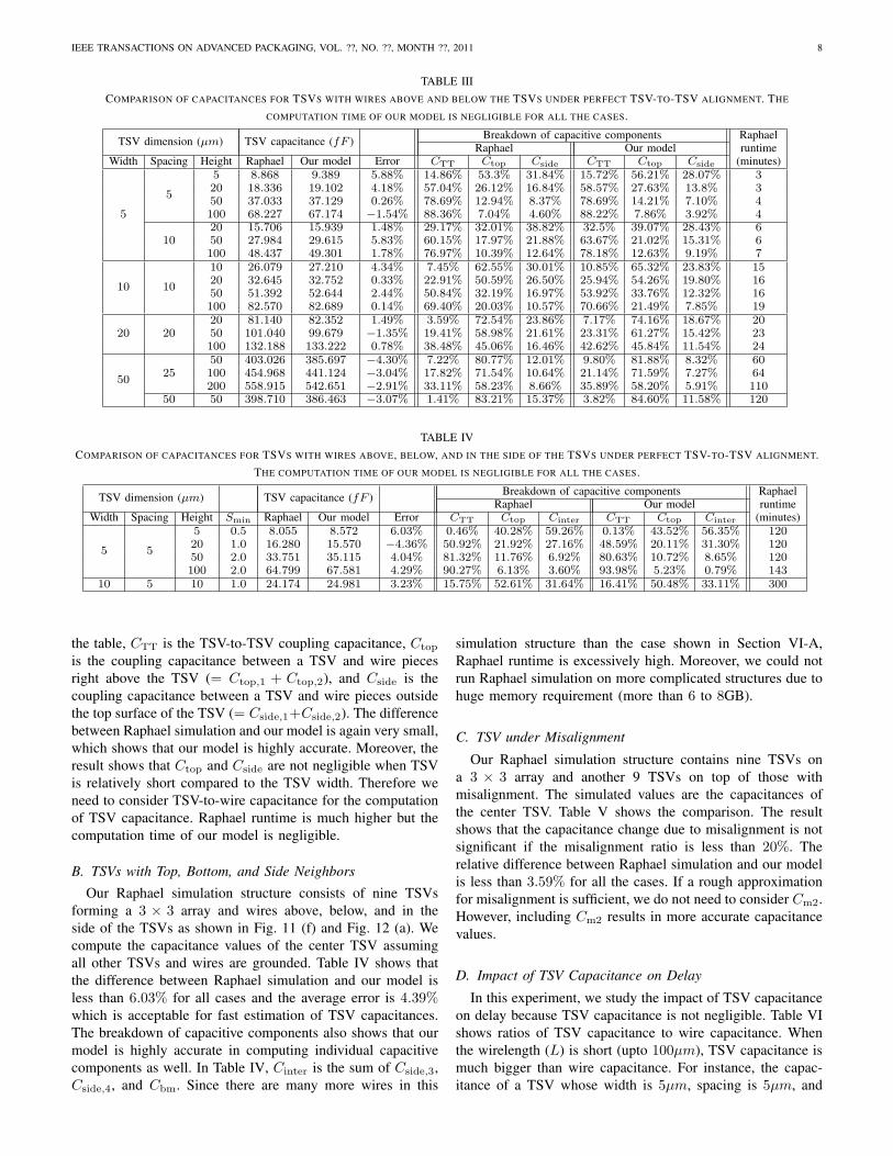
Our Raphael simulation structure consists of nine TSVsforming a 3 × 3 array and wires above and below the TSVsas shown in Fig. 11 (f) and (a). We compute the capacitanceof the center TSV assuming all other TSVs and wires aregrounded. Table III shows capacitances for various TSVdimensions.
We observe that the relative difference between Raphaeland our modeling is less than 5.88% for all the cases andthe average error is 2.51% which is very small. We alsoshow the breakdown of capacitive components to show thatour model for each capacitance component is accurate. In
IEEE TRANSACTIONS ON ADVANCED PACKAGING, VOL. ??, NO. ??, MONTH ??, 2011 8
TABLE IIICOMPARISON OF CAPACITANCES FOR TSVS WITH WIRES ABOVE AND BELOW THE TSVS UNDER PERFECT TSV-TO-TSV ALIGNMENT. THE
COMPUTATION TIME OF OUR MODEL IS NEGLIGIBLE FOR ALL THE CASES.
TSV dimension (µm) TSV capacitance (fF ) Breakdown of capacitive components RaphaelRaphael Our model runtime
Width Spacing Height Raphael Our model Error CTT Ctop Cside CTT Ctop Cside (minutes)
5
5
5 8.868 9.389 5.88% 14.86% 53.3% 31.84% 15.72% 56.21% 28.07% 320 18.336 19.102 4.18% 57.04% 26.12% 16.84% 58.57% 27.63% 13.8% 350 37.033 37.129 0.26% 78.69% 12.94% 8.37% 78.69% 14.21% 7.10% 4100 68.227 67.174 −1.54% 88.36% 7.04% 4.60% 88.22% 7.86% 3.92% 4
1020 15.706 15.939 1.48% 29.17% 32.01% 38.82% 32.5% 39.07% 28.43% 650 27.984 29.615 5.83% 60.15% 17.97% 21.88% 63.67% 21.02% 15.31% 6100 48.437 49.301 1.78% 76.97% 10.39% 12.64% 78.18% 12.63% 9.19% 7
10 10
10 26.079 27.210 4.34% 7.45% 62.55% 30.01% 10.85% 65.32% 23.83% 1520 32.645 32.752 0.33% 22.91% 50.59% 26.50% 25.94% 54.26% 19.80% 1650 51.392 52.644 2.44% 50.84% 32.19% 16.97% 53.92% 33.76% 12.32% 16100 82.570 82.689 0.14% 69.40% 20.03% 10.57% 70.66% 21.49% 7.85% 19
20 2020 81.140 82.352 1.49% 3.59% 72.54% 23.86% 7.17% 74.16% 18.67% 2050 101.040 99.679 −1.35% 19.41% 58.98% 21.61% 23.31% 61.27% 15.42% 23100 132.188 133.222 0.78% 38.48% 45.06% 16.46% 42.62% 45.84% 11.54% 24
5025
50 403.026 385.697 −4.30% 7.22% 80.77% 12.01% 9.80% 81.88% 8.32% 60100 454.968 441.124 −3.04% 17.82% 71.54% 10.64% 21.14% 71.59% 7.27% 64200 558.915 542.651 −2.91% 33.11% 58.23% 8.66% 35.89% 58.20% 5.91% 110
50 50 398.710 386.463 −3.07% 1.41% 83.21% 15.37% 3.82% 84.60% 11.58% 120
TABLE IVCOMPARISON OF CAPACITANCES FOR TSVS WITH WIRES ABOVE, BELOW, AND IN THE SIDE OF THE TSVS UNDER PERFECT TSV-TO-TSV ALIGNMENT.
THE COMPUTATION TIME OF OUR MODEL IS NEGLIGIBLE FOR ALL THE CASES.
TSV dimension (µm) TSV capacitance (fF ) Breakdown of capacitive components RaphaelRaphael Our model runtime
Width Spacing Height Smin Raphael Our model Error CTT Ctop Cinter CTT Ctop Cinter (minutes)
5 5
5 0.5 8.055 8.572 6.03% 0.46% 40.28% 59.26% 0.13% 43.52% 56.35% 12020 1.0 16.280 15.570 −4.36% 50.92% 21.92% 27.16% 48.59% 20.11% 31.30% 12050 2.0 33.751 35.115 4.04% 81.32% 11.76% 6.92% 80.63% 10.72% 8.65% 120100 2.0 64.799 67.581 4.29% 90.27% 6.13% 3.60% 93.98% 5.23% 0.79% 143
10 5 10 1.0 24.174 24.981 3.23% 15.75% 52.61% 31.64% 16.41% 50.48% 33.11% 300
the table, CTT is the TSV-to-TSV coupling capacitance, Ctop
is the coupling capacitance between a TSV and wire piecesright above the TSV (= Ctop,1 + Ctop,2), and Cside is thecoupling capacitance between a TSV and wire pieces outsidethe top surface of the TSV (= Cside,1+Cside,2). The differencebetween Raphael simulation and our model is again very small,which shows that our model is highly accurate. Moreover, theresult shows that Ctop and Cside are not negligible when TSVis relatively short compared to the TSV width. Therefore weneed to consider TSV-to-wire capacitance for the computationof TSV capacitance. Raphael runtime is much higher but thecomputation time of our model is negligible.
B. TSVs with Top, Bottom, and Side Neighbors
Our Raphael simulation structure consists of nine TSVsforming a 3 × 3 array and wires above, below, and in theside of the TSVs as shown in Fig. 11 (f) and Fig. 12 (a). Wecompute the capacitance values of the center TSV assumingall other TSVs and wires are grounded. Table IV shows thatthe difference between Raphael simulation and our model isless than 6.03% for all cases and the average error is 4.39%which is acceptable for fast estimation of TSV capacitances.The breakdown of capacitive components also shows that ourmodel is highly accurate in computing individual capacitivecomponents as well. In Table IV, Cinter is the sum of Cside,3,Cside,4, and Cbm. Since there are many more wires in this
simulation structure than the case shown in Section VI-A,Raphael runtime is excessively high. Moreover, we could notrun Raphael simulation on more complicated structures due tohuge memory requirement (more than 6 to 8GB).
C. TSV under Misalignment
Our Raphael simulation structure contains nine TSVs ona 3 × 3 array and another 9 TSVs on top of those withmisalignment. The simulated values are the capacitances ofthe center TSV. Table V shows the comparison. The resultshows that the capacitance change due to misalignment is notsignificant if the misalignment ratio is less than 20%. Therelative difference between Raphael simulation and our modelis less than 3.59% for all the cases. If a rough approximationfor misalignment is sufficient, we do not need to consider Cm2.However, including Cm2 results in more accurate capacitancevalues.
D. Impact of TSV Capacitance on Delay
In this experiment, we study the impact of TSV capacitanceon delay because TSV capacitance is not negligible. Table VIshows ratios of TSV capacitance to wire capacitance. Whenthe wirelength (L) is short (upto 100µm), TSV capacitance ismuch bigger than wire capacitance. For instance, the capac-itance of a TSV whose width is 5µm, spacing is 5µm, and
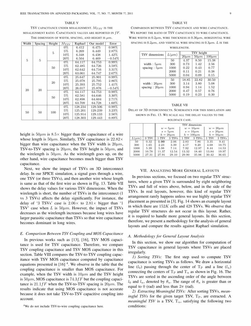
IEEE TRANSACTIONS ON ADVANCED PACKAGING, VOL. ??, NO. ??, MONTH ??, 2011 9
TABLE VTSV CAPACITANCE UNDER MISALIGNMENT. MTSV IS THE
MISALIGNMENT RATIO. CAPACITANCE VALUES ARE REPORTED IN fF .THE DIMENSION OF WIDTH, SPACING, AND HEIGHT IS µm.
Width Spacing Height MTSV Raphael Our model Error
5 5
5
0% 6.412 6.475 0.98%5% 6.269 6.449 2.87%10% 6.348 6.438 1.42%20% 6.504 6.469 −0.54%
50
0% 64.117 64.753 0.99%5% 62.485 64.726 3.59%10% 62.642 64.716 3.31%20% 63.061 64.747 2.67%
20 20
20
0% 25.647 25.901 0.99%5% 25.078 25.795 2.86%10% 25.393 25.752 1.41%20% 26.017 25.876 −0.54%
50
0% 64.117 64.753 0.99%5% 62.581 64.646 3.30%10% 62.898 64.604 2.71%20% 63.709 64.728 1.60%
50 50 100
0% 128.234 129.506 0.99%5% 125.201 129.239 3.23%10% 125.914 129.133 2.56%20% 128.303 129.443 0.89%
height is 50µm is 8.5× bigger than the capacitance of a wirewhose length is 50µm. Similarly, TSV capacitance is 22.82×bigger than wire capacitance when the TSV width is 20µm,TSV-to-TSV spacing is 20µm, the TSV height is 50µm, andthe wirelength is 50µm. As the wirelength goes up, on theother hand, wire capacitance becomes much bigger than TSVcapacitance.
Next, we show the impact of TSVs on 3D interconnectdelay. In our SPICE simulation, a signal goes through a wire,one TSV (or three TSVs), and then another wire whose lengthis same as that of the first wire as shown in Fig. 13. Table VIIshows the delay values for various TSV dimensions. When thewirelength is short, the number of TSVs in the interconnect (1vs 3 TSVs) affects the delay significantly. For instance, thedelay of ‘3 TSVs’ case is 2.06× to 2.81× bigger than ‘1TSV’ case when L is 50µm. However, the impact of TSVsdecreases as the wirelength increases because long wires havelarger parasitic capacitance than TSVs so that wire capacitancebecomes dominant in long wires.
E. Comparison Between TSV Coupling and MOS Capacitance
In previous works such as [13], [16], TSV MOS capaci-tance is used for TSV capacitance. Therefore, we compareTSV coupling capacitance and TSV MOS capacitance in thissection. Table VIII compares the TSV-to-TSV coupling capac-itance with TSV MOS capacitance computed by capacitanceequations presented in [16] 4. We observe in the table that thecoupling capacitance is smaller than MOS capacitance. Forexample, when the TSV width is 10µm and the TSV heightis 50µm, MOS capacitance is 74.3fF but the coupling capaci-tance is 21.1fF when the TSV-to-TSV spacing is 20µm. Theresults indicate that using MOS capacitance is not accuratebecause it does not take TSV-to-TSV capacitive coupling intoaccount.
4We do not include TSV-to-wire coupling capacitance here.
TABLE VICOMPARISON BETWEEN TSV CAPACITANCE AND WIRE CAPACITANCE.WE REPORT THE RATIO OF TSV CAPACITANCE TO WIRE CAPACITANCE.
WIRE WIDTH IS 0.2µm, WIRE THICKNESS IS 0.36µm, HORIZONTAL WIRE
SPACING IS 0.2µm, AND VERTICAL WIRE SPACING IS 0.3µm. L IS THE
WIRELENGTH.
TSV dimensions L(µm)TSV height
20µm 50µm 100µm50 4.37 8.50 15.38
width : 5µm 300 0.73 1.42 2.56spacing : 5µm 1000 0.22 0.43 0.77
2000 0.11 0.21 0.385000 0.04 0.09 0.15
50 18.85 22.82 30.50width : 20µm 300 3.14 3.80 5.08
spacing : 20µm 1000 0.94 1.14 1.522000 0.47 0.57 0.765000 0.19 0.23 0.30
TABLE VIIDELAY OF 3D INTERCONNECTS. SCHEMATICS FOR THIS SIMULATION ARE
SHOWN IN FIG. 13. WE SCALE ALL THE DELAY VALUES TO THE
BOLDFACE CASE.
TSV dimensionsw = 5µm w = 10µm w = 20µms = 5µm s = 10µm s = 20µmh = 20µm h = 100µm h = 50µm
L(µm) 0 TSV 1 TSV 3 TSVs 1 TSV 3 TSVs 1 TSV 3 TSVs50 0.32 1.00 2.06 2.83 7.86 3.35 9.41300 1.65 2.23 3.39 4.17 9.20 4.68 10.751000 5.39 5.98 7.14 7.92 12.97 8.44 14.532000 10.78 11.37 12.54 13.32 18.40 13.84 19.975000 27.31 27.91 29.10 29.90 35.06 30.42 36.65
VII. ANALYZING MORE GENERAL LAYOUTS
In previous sections, we focused on two regular TSV struc-tures, where a given TSV is surrounded by eight neighboringTSVs and full of wires above, below, and in the side of theTSVs. In real layouts, however, this kind of regular TSVarrangement rarely happens unless we use highly regular TSVplacement as presented in [3]. Fig. 14 shows an example layoutin which there are 152K cells and 428 TSVs. We observe thatregular TSV structures do not occur in this layout. Rather,it is required to handle more general layouts. In this section,therefore, we present a methodology for the analysis of generallayouts and compare the results against Raphael simulation.
A. Methodology for General Layout Analysis
In this section, we show our algorithm for computation ofTSV capacitance in general layouts where TSVs are placedirregularly.
1) Sorting TSVs: The first step used to compute TSVcapacitance is sorting TSVs as follows. We draw a horizontalline (l0) passing through the center of TP and a line (ln)connecting the centers of TP and Tn as shown in Fig. 16. TheTSVs are sorted in the ascending order of the angle betweenl0 and ln, denoted by θn. The range of θn is greater than orequal to 0 (rad) and less than 2π (rad).
2) Extracting Meaningful TSVs: After sorting TSVs, mean-ingful TSVs for the given target TSV, TP, are extracted. Ameaningful TSV is a TSV, Tn, satisfying the following twoconditions:
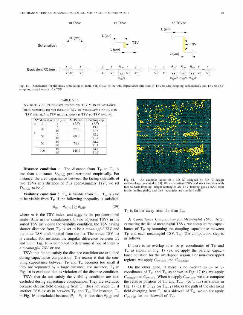
IEEE TRANSACTIONS ON ADVANCED PACKAGING, VOL. ??, NO. ??, MONTH ??, 2011 10
<0 TSV> <1 TSV> <3 TSVs>
Schematics :
Equivalent RC tree :
Fig. 13. Schematics for the delay simulation in Table VII. CTSV is the total capacitance (the sum of TSV-to-wire coupling capacitances and TSV-to-TSVcoupling capacitances) of a TSV.
TABLE VIIITSV-TO-TSV COUPLING CAPACITANCE VS. TSV MOS CAPACITANCE.THESE NUMBERS DO NOT INCLUDE TSV-TO-WIRE CAPACITANCE. w IS
TSV WIDTH, h IS TSV HEIGHT, AND s IS TSV-TO-TSV SPACING.
TSV dimensions (in µm) MOS cap. Coupling cap.w h s (fF ) (fF )
520
527.5
13.410 8.78
505
68.832.2
10 21.2
1050
1074.3
32.220 21.1
10010
148.563.6
20 41.6
Distance condition : The distance from TP to Tn isless than a distance DMAX pre-determined empirically. Forinstance, the area capacitance between the facing sidewalls oftwo TSVs at a distance of d is approximately 1fF , we setDMAX to be d.
Visibility condition : Tn is visible from TP. Tn is saidto be visible from TP if the following inequality is satisfied:
|θm − θm+1| ≥ θMIN (29)
where m is the TSV index, and θMIN is the pre-determinedangle (0.1π in our simulations). If two adjacent TSVs in thesorted TSV list violate the visibility condition, the TSV havingshorter distance from TP is set to be a meaningful TSV andthe other TSV is eliminated from the list. The sorted TSV listis circular. For instance, the angular difference between T8
and T1 in Fig. 16 is computed to determine if one of them isa meaningful TSV or not.
TSVs that do not satisfy the distance condition are excludedduring capacitance computation. The reason is that the cou-pling capacitance between TP and Tn becomes too small ifthey are separated by a large distance. For instance, T4 inFig. 16 is excluded due to violation of the distance condition.
TSVs that do not satisfy the visibility condition are alsoexcluded during capacitance computation. They are excludedbecause electric field diverging from TP does not reach Tn ifanother TSV exists in between TP and Tn. For instance, T7
in Fig. 16 is excluded because |θ6− θ7| is less than θMIN and
Fig. 14. An example layout of a 3D IC designed by 3D IC designmethodology presented in [3]. We use via-first TSVs and stack two dies withface-to-back bonding. Bright rectangles are TSV landing pads (TSVs existinside landing pads), and dark rectangles are standard cells.
T7 is farther away from TP than T6.
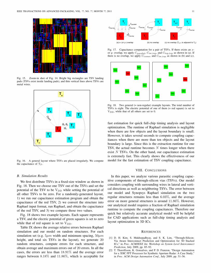
3) Capacitance Computation for Meaningful TSVs: Afterextracting the list of meaningful TSVs, we compute the capac-itance of TP by summing the coupling capacitance betweenTP and each meaningful TSV, Tn. The computation step isas follows.
If there is an overlap in x- or y- coordinates of TP andTn as shown in Fig. 17 (a), we apply the parallel capaci-tance equation for the overlapped region. For non-overlappedregions, we apply Csw,top and Ctop,top.
On the other hand, if there is no overlap in x- or y-coordinates of TP and Tn as shown in Fig. 17 (b), we applyCcorner and Csw,top. When we apply Csw,top, we also comparethe relative position of Tn and Tn+1 (or Tn−1) as shown inFig. 17 (c). If Tn+1 (or Tn−1) blocks the path of the electricalfield diverging from TP to a sidewall of Tn, we do not applyCsw,top for the sidewall of Tn.
IEEE TRANSACTIONS ON ADVANCED PACKAGING, VOL. ??, NO. ??, MONTH ??, 2011 11
Fig. 15. Zoom-in shot of Fig. 14. Bright big rectangles are TSV landingpads (TSVs exist inside landing pads), and thin vertical lines above TSVs aremetal wires.
Fig. 16. A general layout where TSVs are placed irregularly. We computethe capacitance of TP.
B. Simulation Results
We first distribute TSVs in a fixed-size window as shown inFig. 18. Then we choose one TSV out of the TSVs and set thepotential of the TSV to be VDD while setting the potential ofall other TSVs to be zero. For a randomly-generated layout,1) we run our capacitance estimation program and obtain thecapacitance of the red TSV, 2) we convert the structure intoRaphael input format, run Raphael, and obtain the capacitanceof the red TSV, and 3) we compare those two values.
Fig. 18 shows two example layouts. Each square representsa TSV, and the electric potential of green squares is set to zerowhile that of red square is set to VDD.
Table IX shows the average relative errors between Raphaelsimulation and our model on random structures. For eachsimulation set (e.g. 5µm width and minimum spacing, 50µmheight, and total six TSVs in the layout), we generate 20random structures, compute errors for each structure, andobtain average and maximum errors out of 20 errors. In all thecases, the errors are less than 18.91% and the average errorranges between 8.18% and 11.86%, which is acceptable for
Fig. 17. Capacitance computation for a pair of TSVs. If there exists an x-or y- overlap, we apply Cparallel, Csw,top, and Ctop,top as shown in (a). Ifthere is no overlap, we apply Ccorner and Csw,top as shown in (b) and (c).
Fig. 18. Two general (= non-regular) example layouts. The total number ofTSVs is eight. The electric potential of one of them (= red square) is set toVDD, while that of all others are set to 0.
fast estimation for quick full-chip timing analysis and layoutoptimization. The runtime of Raphael simulation is negligiblewhen there are few objects and the layout boundary is small.However, it takes several seconds to compute coupling capac-itances when there are more than ten objects and the layoutboundary is large. Since this is the extraction runtime for oneTSV, the actual runtime becomes N times longer when thereexist N TSVs. On the other hand, our capacitance estimationis extremely fast. This clearly shows the effectiveness of ourmodel for the fast estimation of TSV coupling capacitance.
VIII. CONCLUSIONS
In this paper, we analyze various parasitic coupling capac-itive components of through-silicon vias (TSVs). Our modelconsiders coupling with surrounding wires in lateral and verti-cal directions as well as neighboring TSVs. The error betweenour model and Synopsys Raphael simulation on the tworegular structures remains less than 6.03%, and the averageerror on more general structures is around 11.86%. However,our analytical model requires a fraction of Raphael simulationruntime to compute the coupling capacitances. Therefore ourquick but relatively accurate analytical model will be helpfulfor CAD applications such as full-chip timing analysis andlayout optimization in 3D ICs.
REFERENCES
[1] D. H. Kim, S. Mukhopadhyay, and S. K. Lim, “Through-Silicon-Via Aware Interconnect Prediction and Optimization for 3D StackedICs,” in Proc. ACM/IEEE Int. Workshop on System Level InterconnectPrediction, July 2009, pp. 85–92.
[2] T. Thorolfsson, K. Gonsalves, and P. D. Franzon, “Design Automationfor a 3DIC FFT Processor for Synthetic Aperture Radar: A Case Study,”in Proc. ACM Design Automation Conf., July 2009, pp. 51–56.
IEEE TRANSACTIONS ON ADVANCED PACKAGING, VOL. ??, NO. ??, MONTH ??, 2011 12
TABLE IXCAPACITANCE EXTRACTION ON GENERAL LAYOUTS
TSV dimensions (µm) # TSVs Average Max.Width Min. spacing Height error (%) error (%)
5 5
50
6 8.79 16.158 10.20 15.5910 8.48 14.9212 11.86 15.79
100
6 9.70 15.788 10.49 16.9410 11.20 15.0312 8.53 14.82
10 10
50
6 10.68 16.158 9.36 14.5510 11.44 17.1812 11.22 18.91
100
6 10.10 17.068 9.07 14.6210 10.08 15.4812 8.18 14.79
[3] D. H. Kim, K. Athikulwongse, and S. K. Lim, “A Study of Through-Silicon-Via Impact on the 3D Stacked IC Layout,” in Proc. IEEE Int.Conf. on Computer-Aided Design, Nov. 2009, pp. 674–680.
[4] D. Chen, W. Chiou, M. Chen, T. Wang, K. Ching, et al., “Enabling 3D-IC foundry technologies for 28 nm node and beyond: through-silicon-viaintegration with high throughput die-to-wafer stacking,” in Proc. IEEEInt. Electron Devices Meeting, Dec. 2009.
[5] L. D. Cioccio, P. Gueguen, T. Signamarcheix, M. Rivoire, D. Scevola,et al., “Enabling 3D Interconnects with Metal Direct Bonding,” in Proc.IEEE Int. Interconnect Technology Conference, June 2009, pp. 152–154.
[6] E. Beyne, P. D. Moor, W. Ruythooren, R. Labie, A. Jourdain, et al.,“Through-Silicon Via and Die Stacking Technologies for Microsystems-integration,” in Proc. IEEE Int. Electron Devices Meeting, Dec. 2008.
[7] F. Liu, R. R. Yu, A. M. Young, J. P. Doyle, X. Wang, et al., “A 300-mmWafer-Level Three-Dimensional Integration Scheme Using TungstenThrough-Silicon Via and Hybrid Cu-Adhesive Bonding,” in Proc. IEEEInt. Electron Devices Meeting, Dec. 2008.
[8] J. V. Olmen, A. Mercha, G. Katti, C. Huyghebaert, J. V. Aelst, et al., “3DStacked IC Demonstration using a Through Silicon Via First Approach,”in Proc. IEEE Int. Electron Devices Meeting, Dec. 2008.
[9] G. Katti, A. Mercha, J. V. Olmen, C. Huyghebaert, A. Jourdain, et al.,“3D stacked ICs using Cu TSVs and Die to Wafer Hybrid Collectivebonding,” in Proc. IEEE Int. Electron Devices Meeting, Dec. 2009.
[10] J. Cong and Y. Zhang, “Thermal Via Planning for 3-D ICs,” in Proc.IEEE Int. Conf. on Computer-Aided Design, Nov. 2005, pp. 745–752.
[11] V. F. Pavlidis and E. G. Friedman, “Timing-driven via placementheuristics for three-dimensional ICs,” in Integration, the VLSI Journal,vol. 41, no. 4, July 2008, pp. 489–508.
[12] D. Khalil, Y. Ismail, M. Khellah, T. Karnik, and V. De, “AnalyticalModel for the Propagation Delay of Through Silicon Vias,” in Proc. Int.Symp. on Quality Electronic Design, Mar. 2008, pp. 553–556.
[13] I. Savidis and E. G. Friedman, “Closed-Form Expressions of 3-D ViaResistance, Inductance, and Capacitance,” in IEEE Trans. on ElectronDevices, vol. 56, no. 9, Sept. 2009, pp. 1873–1881.
[14] T. Bandyopadhyay, R. Chatterjee, D. Chung, M. Swaminathan, andR. Tummala, “Electrical Modeling of Through Silicon and PackageVias,” in Proc. IEEE Int. Conf. on 3D System Integration, Sept. 2009.
[15] C. Xu, H. Li, R. Suaya, and K. Banerjee, “Compact AC Modeling andAnalysis of Cu, W, and CNT based Through-Silicon Vias (TSVs) in 3-DICs,” in Proc. IEEE Int. Electron Devices Meeting, Dec. 2009.
[16] G. Katti, M. Stucchi, K. D. Meyer, and W. Dehaene, “Electrical Model-ing and Characterization of Through Silicon via for Three-DimensionalICs,” in IEEE Trans. on Electron Devices, vol. 57, no. 1, Jan. 2010, pp.256–262.
[17] D. H. Kim, S. Mukhopadhyay, and S. K. Lim, “TSV-aware InterconnectLength and Power Prediction for 3D Stacked ICs,” in Proc. IEEE Int.Interconnect Technology Conference, June 2002, pp. 26–28.
[18] D. H. Kim and S. K. Lim, “Through-Silicon-Via-aware Delay andPower Prediction Model for Buffered Interconnects in 3D ICs,” in Proc.ACM/IEEE Int. Workshop on System Level Interconnect Prediction, June2010.
[19] K. Yoon, G. Kim, W. Lee, T. Song, J. Lee, et al., “Modeling and Analysisof Coupling between TSVs, Metal, and RDL interconnects in TSV-
based 3D IC with Silicon Interposer,” in Proc. Electronics PackagingTechnology Conference, Dec. 2009, pp. 702–706.
[20] T. Sakurai and K. Tamaru, “Simple Formulas for Two- and Three-Dimensional Capacitances,” in IEEE Trans. on Electron Devices, vol. 30,no. 2, Feb. 1983, pp. 183–185.
[21] A. Bansal, B. C. Paul, and K. Roy, “An Analytical Fringe CapacitanceModel for Interconnects Using Conformal Mapping,” in IEEE Trans.on Computer-Aided Design of Integrated Circuits and Systems, vol. 25,no. 12, Dec. 2006, pp. 2765–2774.
[22] H. C. Ohanian and J. T. Markert, Physics for Engineers and Scientists.W. W. Norton & Company, 2007.
[23] A. W. Topol, J. D. C. La Tulipe, L. Shi, D. J. Frank, K. Bernstein, et al.,“Three-dimensional Integrated Circuits,” in IBM J. Res. & Dev., vol. 50,no. 4, July 2006, pp. 491–506.
[24] Synopsys, “Raphael,” http://www.synopsys.com.
Dae Hyun Kim (S’08) received the B.S. degreein electrical engineering from Seoul National Uni-versity, Seoul, Korea, in 2002, and received theM.S. degree in electrical and computer engineeringfrom Georgia Institute of Technology, Atlanta, GAin 2007. Currently, he is working toward the Ph.D.degree in the School of Electrical and Computer En-gineering, Georgia Institute of Technology, Atlanta,GA. His research interests are physical design al-gorithms for 3D ICs including design methodology,placement, routing, and design for manufacturability.
Saibal Mukhopadhyay (S’00-M’07) received theB.E. degree in electronics and telecommunicationengineering from Jadavpur University, Calcutta, In-dia, in 2000 and the Ph.D. degree in electricaland computer engineering from Purdue University,West Lafayette, IN, in 2006. He is with the Schoolof Electrical and Computer Engineering, GeorgiaInstitute of Technology, Atlanta, as an AssistantProfessor. Prior to joining Georgia Tech, he waswith the IBM T. J. Watson Research Center, York-town Heights, NY as a Research Staff Member. His
research interests include low-power variation tolerant VLSI circuits andsystems, embedded systems, and 3D integration. He has (co)-authored over90 papers in refereed journals and conferences.
Dr. Mukhopadhyay was a recipient of the IBM Faculty Partnership Awardfor 2009 and 2010, SRC Inventor Recognition Award in 2009, SRC TechnicalExcellence Award in 2005, IBM PhD Fellowship Award for 2004-2005, theBest in Session Award at 2005 SRC TECNCON, Best Paper Awards at 2003IEEE Nano and 2004 International Conference on Computer Design.
IEEE TRANSACTIONS ON ADVANCED PACKAGING, VOL. ??, NO. ??, MONTH ??, 2011 13
Sung Kyu Lim (S’94-M’00-SM’05) received theB.S., M.S., and Ph.D. degrees from the ComputerScience Department, University of California, LosAngeles (UCLA), in 1994, 1997, and 2000, respec-tively. From 2000 to 2001, he was a Post-DoctoralScholar at UCLA, and a Senior Engineer at AplusDesign Technologies, Inc. He joined the School ofElectrical and Computer Engineering, Georgia Insti-tute of Technology in 2001, where he is currentlyan Associate Professor. His research focus is on thephysical design automation for 3D ICs, 3D System-
in-Packages, microarchitectural physical planning, and field-programmableanalog arrays. He is the author of Practical Problems in VLSI Physical DesignAutomation (Springer, 2008).
Dr. Lim received the Design Automation Conference (DAC) GraduateScholarship in 2003 and the National Science Foundation Faculty Early CareerDevelopment (CAREER) Award in 2006. He was on the Advisory Boardof the ACM Special Interest Group on Design Automation (SIGDA) during2003-2008 and received the ACM SIGDA Distinguished Service Award in2008. He is currently an Associate Editor of the IEEE Transactions on VeryLarge Scale Integration Systems (TVLSI) and served as a Guest Editor for theACM Transactions on Design Automation of Electronic Systems (TODAES).He has served the Technical Program Committee of several ACM and IEEEconferences on electronic design automation.


![1 Lecture 3: Transactions and Recovery Transactions (ACID) Recovery Advanced Databases CG096 Nick Rossiter [Emma-Jane Phillips-Tait]](https://img.pdfslide.net/doc/110x75/5697bf991a28abf838c91b72/1-lecture-3-transactions-and-recovery-transactions-acid-recovery-advanced.jpg)