Embed Size (px)
Citation preview
Degree project in
Implementation of DC-DC converterwith maximum power point tracking
controlfor thermoelectric generator applications
DAVID JAHANBAKHSH
Stockholm, Sweden 2012
XR-EE-E2C 2012:015
Electrical EngineeringMaster of Science
Implementation of DC-DC converter withmaximum power point tracking control for
thermoelectric generator applications
DAVID JAHANBAKHSH
Supervisor
Jan Dellrud, Scania CV AB
Examiner
Prof. Hans-Peter Nee, E2C, KTH
Master ThesisRoyal Institute of Technology (KTH)
School of Electrical EngineeringElectrical Energy Conversion
Stockholm 2012XR-EE-E2C 2012:015

Abstract
A heavy duty vehicle looses approximately 30-40 % of the energy in the fuel as wasteheat through the exhaust system. Recovering this waste heat would make the vehiclemeet the legislative and market demands of emissions and fuel consumption easier.This recovery is possible by transforming the waste heat to electric power using a thermo-electric generator. However, the thermoelectric generator electric characteristics makesdirect usage of it unprofitable, thus an electric power conditioner is necessary.
First a study of different DC-DC converters is presented, based on that the most suit-able converter for thermoelectric application is determined. In order to maximize theharvested power, maximum power point tracking algorithms have been studied and an-alyzed.After the investigation, the single ended primary inductor converter was simulated andimplemented with a perturb and observe algorithm, and the incremental conductance al-gorithm. The converter was tested with a 20 W thermoelectric generator, and evaluated.The results show that the incremental conductance is more robust and stable comparedto the perturb and observe algorithm. Further on, the incremental conductance also hasa higher average efficiency during real implementation.
Keywords: Thermoelectric generator, Waste heat recovery, DC-DC converter, singleended primary inductor converter, Maximum power point tracking, Perturb and observe,Incremental conductance.
ii

Sammanfattning
En lastbil forlorar ungefar 30-40 % av energin fran branslet i form av spillvarme i avgas-systemet. Att kunna atervinna denna spillvarme skulle fa fordonet att lattare uppfyllaframtida rattsliga och marknadskrav pa utslapp och bransleforbrukning.Med en termoelektrisk generator ar denna atervinning mojlig, genom att omvandlaspillvarme till elektrisk effekt. Dock har termoelektriska generatorn dalig elektrisk ka-rakteristik, vilket medfor att direkt inkoppling ar olonsamt. Darfor kravs en elektriskomvandlare for att pa ett effektivt satt atervinna energin.
Denna rapport presenterar forst en studie av olika DC-DC-omvandlare, baserat pa dennastudie bestams den mest lampliga omvandlare for termoelektriska generatorn.For att maximera den atervunna effekten har tva maximala effekt punkt algoritmer stu-derats och analyserats.Efter undersokningen utfordes simulering och implementering av single ended prima-ry inductor omvandlaren, med perturbe and observe algoritmen samt incremental con-ductance algoritmen. Omvandlaren testades med en 20 W termoelektrisk generator, ochutvarderades. Resultaten visar att incremental conductance algoritmen ar mer robustoch stabil jamfort med perturbe and observe algoritmen. Dessutom har incremental con-ductance algoritmen ocksa en hogre genomsnittlig verkningsgrad under implementering.
iii


Acknowledgements
This thesis finalizes my Master of Science degree in Electrical Engineering atthe Royal Institute of Technology (KTH) in Stockholm, Sweden.This work has been conducted between April 2012 and September 2012 at thePre-development department (REP) at Scania CV AB in Sodertalje, Sweden and wassupervised at the Electrical Engineering Department at KTH.
First, I would like to express my gratitude to my supervisor at Scania, Jan Dellrud, forhis valuable time, support and guidance he has given me throughout the whole project.I also want to thank Jan Hellgren at Scania, for his help, support and vast knowledge.I also want to express my gratitude to my supervisor at KTH, Hans-Peter Nee, for hiswise inputs and feedback.Many thanks go to everyone at REP, at Scania for the great atmosphere and the warmwelcoming.Finally, I would like to thank my family, in particular my parents. Without their supportI would not have been able to accomplish anything.
v

Contents
Abstract ii
Abstract iii
List of Figures ix
List of Tables xi
Nomenclature xii
1 Introduction 1
1.1 Background . . . . . . . . . . . . . . . . . . . . . . . . . . . . . . . . . . . 1
1.2 Related work . . . . . . . . . . . . . . . . . . . . . . . . . . . . . . . . . . 1
1.3 Thesis objective and delimitations . . . . . . . . . . . . . . . . . . . . . . 2
1.4 Thesis outline . . . . . . . . . . . . . . . . . . . . . . . . . . . . . . . . . . 2
2 The thermoelectric generator 3
2.1 The thermoelectric effect . . . . . . . . . . . . . . . . . . . . . . . . . . . . 3
2.2 Figure of merit . . . . . . . . . . . . . . . . . . . . . . . . . . . . . . . . . 4
2.3 Equivalent circuit of TEG . . . . . . . . . . . . . . . . . . . . . . . . . . . 5
2.4 System overview . . . . . . . . . . . . . . . . . . . . . . . . . . . . . . . . 8
2.5 TEG in vehicles . . . . . . . . . . . . . . . . . . . . . . . . . . . . . . . . . 8
3 DC-DC Converters 11
3.1 DC-DC Converters . . . . . . . . . . . . . . . . . . . . . . . . . . . . . . . 11
3.2 Control of DC-DC converters . . . . . . . . . . . . . . . . . . . . . . . . . 11
3.3 The Buck-Boost Converter . . . . . . . . . . . . . . . . . . . . . . . . . . 13
3.4 Cuk Converter . . . . . . . . . . . . . . . . . . . . . . . . . . . . . . . . . 14
3.5 SEPIC converter . . . . . . . . . . . . . . . . . . . . . . . . . . . . . . . . 16
3.6 Full bridge converter . . . . . . . . . . . . . . . . . . . . . . . . . . . . . . 18
3.7 Continuos and Discontinuos conduction mode . . . . . . . . . . . . . . . . 19
3.8 Design of converters . . . . . . . . . . . . . . . . . . . . . . . . . . . . . . 20
3.8.1 Buck-Boost converter . . . . . . . . . . . . . . . . . . . . . . . . . 20
3.8.2 Cuk converter . . . . . . . . . . . . . . . . . . . . . . . . . . . . . . 21
vii
3.8.3 SEPIC converter . . . . . . . . . . . . . . . . . . . . . . . . . . . . 223.8.4 Fullbridge converter . . . . . . . . . . . . . . . . . . . . . . . . . . 23
3.9 Dimensioning of TEG module . . . . . . . . . . . . . . . . . . . . . . . . . 243.10 Summary . . . . . . . . . . . . . . . . . . . . . . . . . . . . . . . . . . . . 25
4 Maximum power point control 274.1 MPPT control . . . . . . . . . . . . . . . . . . . . . . . . . . . . . . . . . 27
4.1.1 Perturb and observe . . . . . . . . . . . . . . . . . . . . . . . . . . 274.1.2 Incremental conductance . . . . . . . . . . . . . . . . . . . . . . . 28
5 Simulation 315.1 Simulation . . . . . . . . . . . . . . . . . . . . . . . . . . . . . . . . . . . . 315.2 Modelling of the TEG . . . . . . . . . . . . . . . . . . . . . . . . . . . . . 315.3 Measurements . . . . . . . . . . . . . . . . . . . . . . . . . . . . . . . . . . 325.4 Model limitations and simplifications . . . . . . . . . . . . . . . . . . . . . 375.5 Driving cycle simulation . . . . . . . . . . . . . . . . . . . . . . . . . . . . 385.6 Simulation settings . . . . . . . . . . . . . . . . . . . . . . . . . . . . . . . 395.7 MPPT algorithms . . . . . . . . . . . . . . . . . . . . . . . . . . . . . . . 405.8 Efficiency mapping . . . . . . . . . . . . . . . . . . . . . . . . . . . . . . . 41
6 Implementation 436.1 Current sensor . . . . . . . . . . . . . . . . . . . . . . . . . . . . . . . . . 436.2 Voltage sensor . . . . . . . . . . . . . . . . . . . . . . . . . . . . . . . . . . 446.3 MOSFET-switch . . . . . . . . . . . . . . . . . . . . . . . . . . . . . . . . 456.4 Complete converter . . . . . . . . . . . . . . . . . . . . . . . . . . . . . . . 466.5 Converter control . . . . . . . . . . . . . . . . . . . . . . . . . . . . . . . . 47
7 Results 497.1 Simulation results . . . . . . . . . . . . . . . . . . . . . . . . . . . . . . . 497.2 Implementation results . . . . . . . . . . . . . . . . . . . . . . . . . . . . . 51
8 Conclusion 53
9 Discussion 55
Bibliography 57
Appendices 59
viii
List of Figures
2.1 Two dissimilar materials joint at different temperatures, forming a circuit. 3
2.2 A p- and n-doped material connected electrically in series and thermallyin parallel. . . . . . . . . . . . . . . . . . . . . . . . . . . . . . . . . . . . . 4
2.3 Several thermocouples connected in series, yielding a larger net voltage. . 4
2.4 Equivalent circuit of a TEG. . . . . . . . . . . . . . . . . . . . . . . . . . 5
2.5 TEG connected to a variable load. . . . . . . . . . . . . . . . . . . . . . . 5
2.6 Pl and Pint plotted as a function of load resistance. . . . . . . . . . . . . . 6
2.7 Pl and Pint plotted as a function of Is. . . . . . . . . . . . . . . . . . . . . 7
2.8 I-U characteristics. . . . . . . . . . . . . . . . . . . . . . . . . . . . . . . . 8
2.9 TEG unit connected to a converter and load. . . . . . . . . . . . . . . . . 8
2.10 Typical energy path for a combustion engine[2]. . . . . . . . . . . . . . . . 9
2.11 Basic model of a TEG module implemented in a HDV electrical system. . 9
3.1 Ideal switching DC converter. . . . . . . . . . . . . . . . . . . . . . . . . . 11
3.2 Comparator generating PWM signal. . . . . . . . . . . . . . . . . . . . . . 12
3.3 Generation of the PWM signal for the transistor switch. . . . . . . . . . . 13
3.4 Buck-Boost converter. . . . . . . . . . . . . . . . . . . . . . . . . . . . . . 13
3.5 Equivalent circuit of the Buck-Boost converter during on- and off-state ofswitch. . . . . . . . . . . . . . . . . . . . . . . . . . . . . . . . . . . . . . . 14
3.6 Cuk converter. . . . . . . . . . . . . . . . . . . . . . . . . . . . . . . . . . 15
3.7 Equivalent circuit of the Cuk converter during on- and off-state of switch. 15
3.8 SEPIC converter. . . . . . . . . . . . . . . . . . . . . . . . . . . . . . . . . 16
3.9 Equivalent circuit of the SEPIC converter during on- and off-state of switch. 17
3.10 example caption . . . . . . . . . . . . . . . . . . . . . . . . . . . . . . . . 18
3.11 Waveforms for continuos- and discontinous-conduction mode. . . . . . . . 19
3.12 Buck-Boost converter connected to TEG and battery. . . . . . . . . . . . 21
3.13 Cukconverter connected to TEG and battery. . . . . . . . . . . . . . . . . 22
3.14 SEPIC converter connected to TEG and battery. . . . . . . . . . . . . . . 22
3.15 Fullbridge converter connected to TEG and battery. . . . . . . . . . . . . 23
3.16 TEG module represented as a matrix and equivalent circuit. . . . . . . . . 24
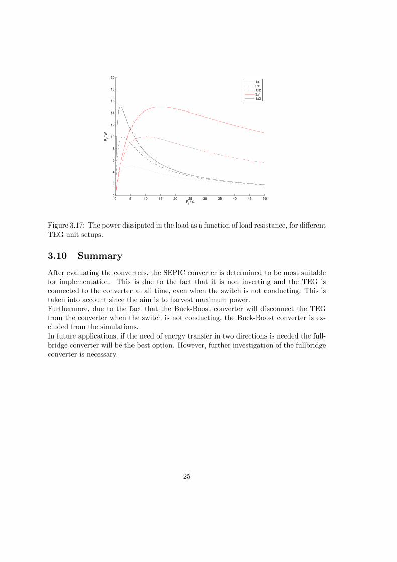
3.17 The power dissipated in the load as a function of load resistance, fordifferent TEG unit setups. . . . . . . . . . . . . . . . . . . . . . . . . . . . 25
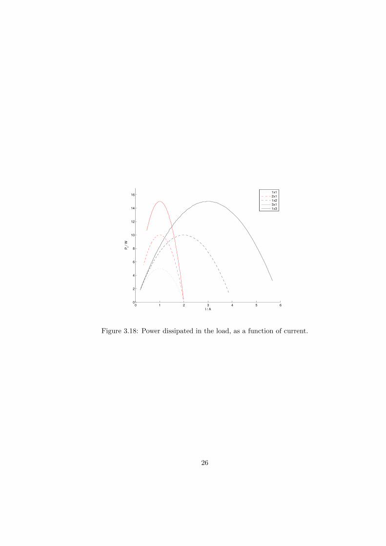
3.18 Power dissipated in the load, as a function of current. . . . . . . . . . . . 26
ix
4.1 Operation of perturb and observe control. . . . . . . . . . . . . . . . . . . 284.2 Perturbe and observe algorithm flowchart, where k is the sample. . . . . . 294.3 Incremental conductance algorithm flowchart, where k is the sample. . . . 304.4 Operation of incremental conductance control. . . . . . . . . . . . . . . . 30
5.1 The test circuit. . . . . . . . . . . . . . . . . . . . . . . . . . . . . . . . . . 325.2 P-I curve plotted for different ∆T . . . . . . . . . . . . . . . . . . . . . . . 335.3 U-I curve plotted for different ∆T . . . . . . . . . . . . . . . . . . . . . . . 345.4 Voltage plotted as a function of Th and ∆T . . . . . . . . . . . . . . . . . . 355.5 Internal resistance as a function of ∆T . . . . . . . . . . . . . . . . . . . . 365.6 Internal resistance as a function of T = Th+Tc
2 . . . . . . . . . . . . . . . . 365.7 Simulink model of openload voltage and internal resistance. . . . . . . . . 375.8 Simulink model of TEG. . . . . . . . . . . . . . . . . . . . . . . . . . . . . 375.9 Comparison of model generated Uol and Rint. . . . . . . . . . . . . . . . . 375.10 Output power for P&O and INC with different update rate and ∆D for
the SEPIC converter. . . . . . . . . . . . . . . . . . . . . . . . . . . . . . . 405.11 Efficiency mapping for P&O and INC algorithm for the SEPIC converter. 41
6.1 Current sensing circuit. . . . . . . . . . . . . . . . . . . . . . . . . . . . . 446.2 Voltage divider used for voltage measurements. . . . . . . . . . . . . . . . 446.3 Driver circuit for the MOSFET transistor. . . . . . . . . . . . . . . . . . . 456.4 Implemented SEPIC converter. . . . . . . . . . . . . . . . . . . . . . . . . 46
7.1 Segment of the output power of the SEPIC converter for the Spain drivecycle. . . . . . . . . . . . . . . . . . . . . . . . . . . . . . . . . . . . . . . . 50
7.2 Segment of the output power of the SEPIC converter for the Brusselsdrive cycle. . . . . . . . . . . . . . . . . . . . . . . . . . . . . . . . . . . . 51
1 The thermoelectric generator used in the project. . . . . . . . . . . . . . . 612 The model generating the hot side temperature from driving cycle data [1]. 613 A section of the torque plot from the Brussels driving cycle. . . . . . . . . 624 A section of the temperature plot from the Brussels driving cycle. . . . . . 625 The recovered energy in kWh, from the Brussels driving cycle. . . . . . . 636 A section of the torque plot from the Spain driving cycle. . . . . . . . . . 637 A section of the temperature plot from the Spain driving cycle. . . . . . . 648 The recovered energy in kWh, from the Spain driving cycle. . . . . . . . . 649 The complete model. . . . . . . . . . . . . . . . . . . . . . . . . . . . . . . 6510 The SEPIC-converter model. . . . . . . . . . . . . . . . . . . . . . . . . . 6511 The perturb and observe algorithm model. . . . . . . . . . . . . . . . . . . 6612 The incremental conductance algorithm model. . . . . . . . . . . . . . . . 6613 The mapping model. . . . . . . . . . . . . . . . . . . . . . . . . . . . . . . 6614 The SEPIC-converter. . . . . . . . . . . . . . . . . . . . . . . . . . . . . . 6715 The Arduino UNO micro controller. . . . . . . . . . . . . . . . . . . . . . 68
x

List of Tables
6.1 Outputs and inputs. . . . . . . . . . . . . . . . . . . . . . . . . . . . . . . 466.2 Component values and ratings. . . . . . . . . . . . . . . . . . . . . . . . . 47
7.1 Simulated efficiencies of the two algorithms during the two driving cycles. 507.2 Simulated and measured average efficiencies of the converter for the two
different algorithms. . . . . . . . . . . . . . . . . . . . . . . . . . . . . . . 51
1 Components used in the converter. . . . . . . . . . . . . . . . . . . . . . . 67
xi

Nomenclature
D Duty ratio [-]∆D Duty ratio step [-]fs Switching frequency [Hz]Is Source current [A]K Kelvin [K]P Power [W]R Resistance [Ω]Rint Internal resistance [Ω]Rl Load resistance [Ω]T Temperature [oC]Tc Cold side temperature [oC]Th Hot side temperature [oC]Ts Switch period [s]toff Off time of switch [s]ton On time of switch [s]ts Algorithm update period [s]∆T Temperature difference [oC]U Voltage [V ]Ubat Battery voltage [V ]Uin Input voltage [V ]Uo Output voltage [V ]Uol Openload voltage [V ]Upwm Pulse width voltage [V ]Uref Reference voltage [V ]Utri Triangle voltage [V ]
α Seebeck coefficient [ VK ]ZT Figure of merit [-]
xii

Chapter 1
Introduction
1.1 Background
Fossil fuel engines are the main source of energy for vehicles today. However, approx-imately 40 % of the energy in the fuel is lost through the exhaust system as wasteheat[2]. For commercial vehicles, in this case heavy duty vehicles (HDV), the legislativeand market of emissions and fuel consumption are becoming harder to meet. Hence, thepossibility to recover this heat is of high interest.
For waste heat recovery, based on the Seebeck effect[3], the thermoelectric generator(TEG) is a great candidate. Mainly because it has no moving parts and does not requirecomplex machinery to convert the heat energy to electrical energy.Today the technique is still premature and efficiency has not yet reached a level thatmakes the technology profitable.However new materials are being developed that increase efficiency and are more envi-ronmental friendly. This allows TEG technology to be a great candidate for waste heatrecovery, compared to other technologies.
1.2 Related work
In the recent years the TEG technology for different applications has been in the spot-light. When it comes to the vehicle industry, major car companies are researching in thearea. However, in the area of HDV the technology has not been focused on. Although,some publications have been published, where companies have implemented TEG unitsin a HDV engine. However, the actual implementation during driving cycles has notbeen investigated and published. Previous experiments and studies show that this tech-nology have great potential to harvest electrical energy from the waste heat of engines,for instance, Hi-Z Technology Inc. developed a TEG for diesel engines, that was able todeliver 1 kW of power [4]. Todays TEGs have an efficiency on the order of 5 % [3], inorder to be able to use TEGs profitably, some kind of electrical conditioner is necessary.Furthermore, TEGs have been able to reduce fuel consumtion with 10 %, by replacing a
1
significant portion of the electric power produced by the alternator[5]. This shows thatthe usage of a TEG in a vehicle is very interesting.Previously in a thesis work a DC-DC converter with constant output voltage has beenimplemented and evaluated [6], however no MPPT controlled converter has yet beeninvestigated at Scania CV.
1.3 Thesis objective and delimitations
There has been sufficient research in TEG technology in vehicle applications, howevernot very much regarding HDV. The research is mainly focused on harvesting energyrather than conditioning it after the harvesting.The idea of maximizing the harvested power and effectively using it, has been well in-vestigated in the photovoltaic area[7]. Nevertheless, when it comes to TEGs, furtherresearch and analyze is required.The objectives of this master thesis has been to design, implement and present a powerconditioner to extract maximum electrical power from a TEG unit that previously hasbeen developed at Scania.The power conditioner is a DC-DC converter that is controlled with a maximum powerpoint tracking algorithm (MPPT). Furthermore, the focus in this thesis has been on theMPPT algorithms.The efficiency and cost of the implemented converter has also been investigated. Fi-nally the work has been concluded with suggestions of further investigation and futurepossibilities.
1.4 Thesis outline
The thesis is structured as followed: chapters 2 and 3 describe the TEG and DC-DCconverters. Furthermore, chapter 4 gives an overview over MPPT algorithms, mainlythe perturb and observe algorithm and the incremental conductance algorithm.Chapter 5 describes the modelling of the TEG that was used, and the simulated results.In chapter 6, the implemented SEPIC converter is presented and in chapter 7 the re-sults are described. Finally, chapter 8 and 9 summarises the project along with somesuggestions to future work.
2
Chapter 2
The thermoelectric generator
2.1 The thermoelectric effect
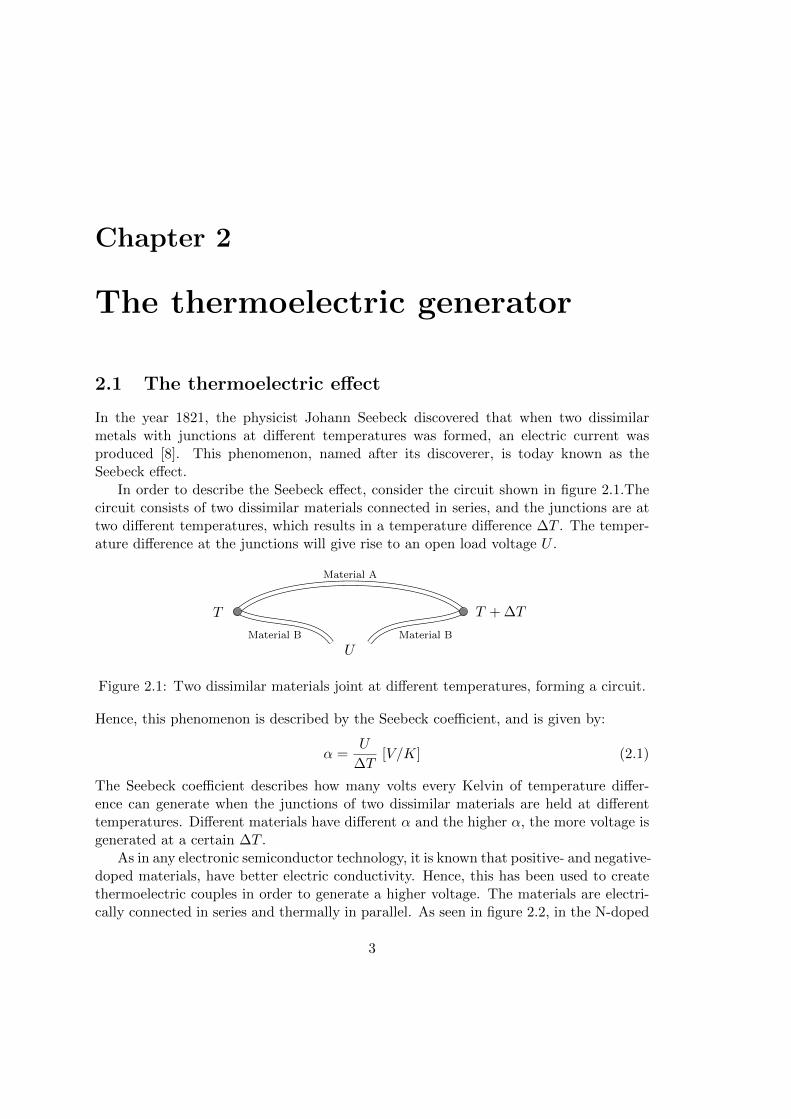
In the year 1821, the physicist Johann Seebeck discovered that when two dissimilarmetals with junctions at different temperatures was formed, an electric current wasproduced [8]. This phenomenon, named after its discoverer, is today known as theSeebeck effect.
In order to describe the Seebeck effect, consider the circuit shown in figure 2.1.Thecircuit consists of two dissimilar materials connected in series, and the junctions are attwo different temperatures, which results in a temperature difference ∆T . The temper-ature difference at the junctions will give rise to an open load voltage U .
T T + ∆T
U
Material A
Material B Material B
Figure 2.1: Two dissimilar materials joint at different temperatures, forming a circuit.
Hence, this phenomenon is described by the Seebeck coefficient, and is given by:
α =U
∆T[V/K] (2.1)
The Seebeck coefficient describes how many volts every Kelvin of temperature differ-ence can generate when the junctions of two dissimilar materials are held at differenttemperatures. Different materials have different α and the higher α, the more voltage isgenerated at a certain ∆T .
As in any electronic semiconductor technology, it is known that positive- and negative-doped materials, have better electric conductivity. Hence, this has been used to createthermoelectric couples in order to generate a higher voltage. The materials are electri-cally connected in series and thermally in parallel. As seen in figure 2.2, in the N-doped
3
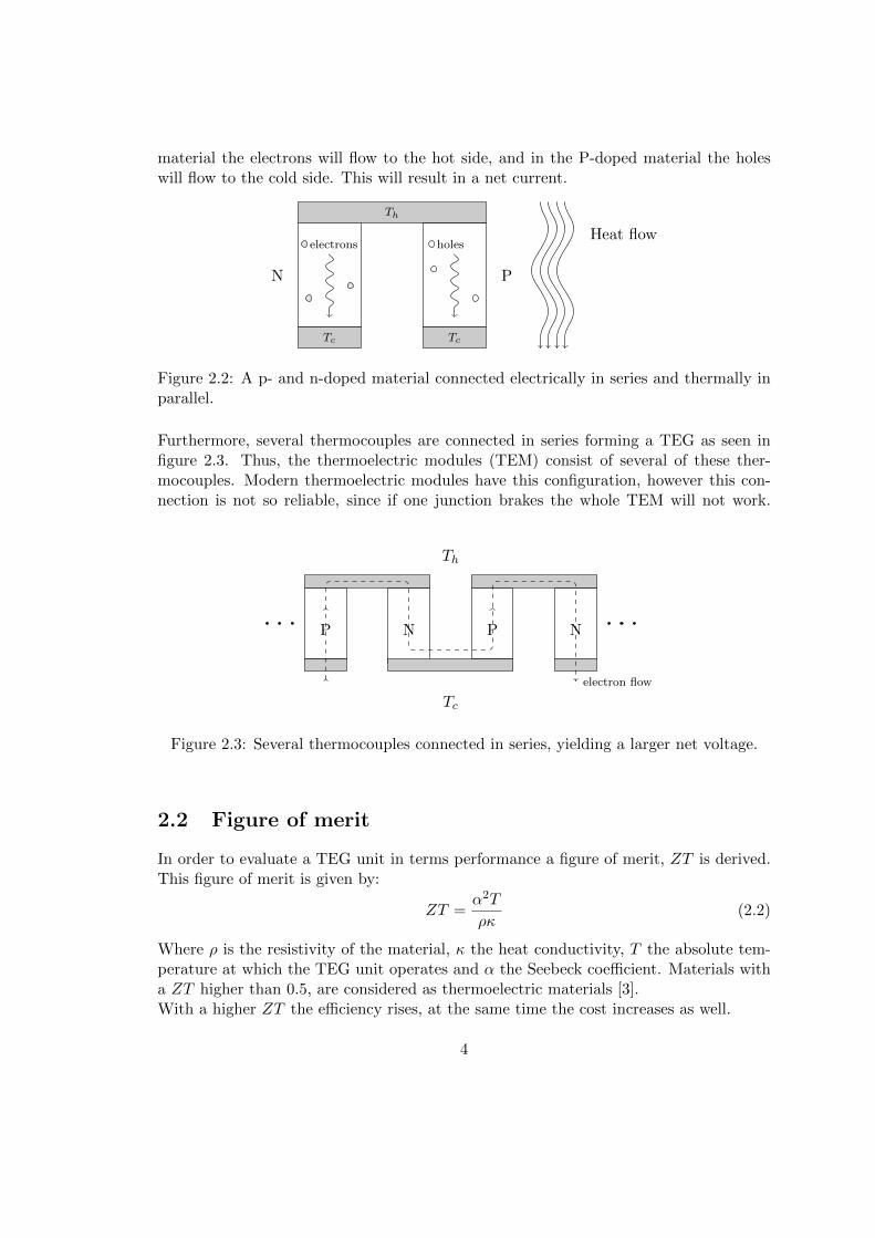
material the electrons will flow to the hot side, and in the P-doped material the holeswill flow to the cold side. This will result in a net current.
Th
Tc Tc
Heat flowelectrons holes
N P
Figure 2.2: A p- and n-doped material connected electrically in series and thermally inparallel.
Furthermore, several thermocouples are connected in series forming a TEG as seen infigure 2.3. Thus, the thermoelectric modules (TEM) consist of several of these ther-mocouples. Modern thermoelectric modules have this configuration, however this con-nection is not so reliable, since if one junction brakes the whole TEM will not work.
Th
Tc
P N P N
electron flow
Figure 2.3: Several thermocouples connected in series, yielding a larger net voltage.
2.2 Figure of merit
In order to evaluate a TEG unit in terms performance a figure of merit, ZT is derived.This figure of merit is given by:
ZT =α2T
ρκ(2.2)
Where ρ is the resistivity of the material, κ the heat conductivity, T the absolute tem-perature at which the TEG unit operates and α the Seebeck coefficient. Materials witha ZT higher than 0.5, are considered as thermoelectric materials [3].With a higher ZT the efficiency rises, at the same time the cost increases as well.
4
This makes TEG less common in applications due to its manufacturing cost and theoverall profitability in terms of harvested energy.
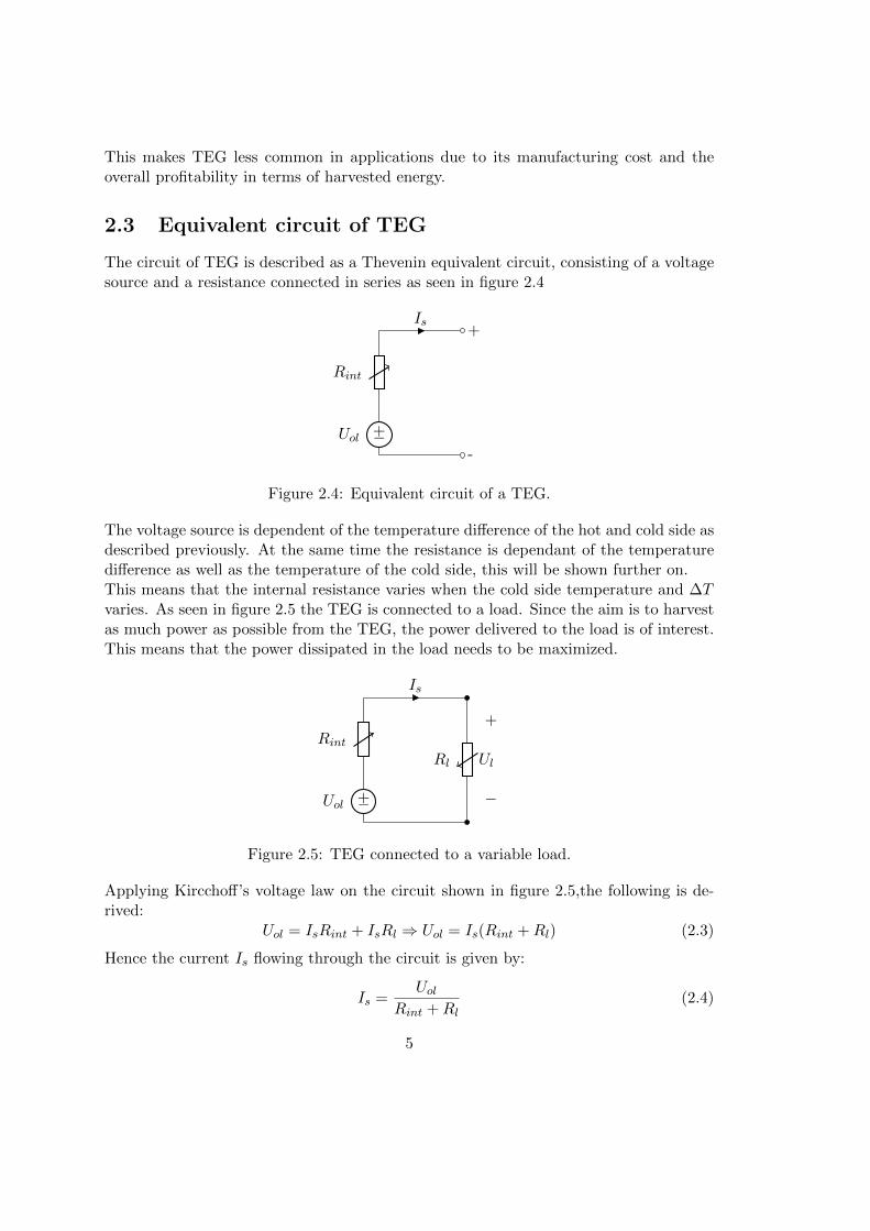
2.3 Equivalent circuit of TEG
The circuit of TEG is described as a Thevenin equivalent circuit, consisting of a voltagesource and a resistance connected in series as seen in figure 2.4
-
+−Uol
Rint
Is+
Figure 2.4: Equivalent circuit of a TEG.
The voltage source is dependent of the temperature difference of the hot and cold side asdescribed previously. At the same time the resistance is dependant of the temperaturedifference as well as the temperature of the cold side, this will be shown further on.This means that the internal resistance varies when the cold side temperature and ∆Tvaries. As seen in figure 2.5 the TEG is connected to a load. Since the aim is to harvestas much power as possible from the TEG, the power delivered to the load is of interest.This means that the power dissipated in the load needs to be maximized.
+−Uol
Rint
Is
Rl
+
−
Ul
Figure 2.5: TEG connected to a variable load.
Applying Kircchoff’s voltage law on the circuit shown in figure 2.5,the following is de-rived:
Uol = IsRint + IsRl ⇒ Uol = Is(Rint +Rl) (2.3)
Hence the current Is flowing through the circuit is given by:
Is =Uol
Rint +Rl(2.4)
5
Furthermore, using equation (2.4) the power dissipated in the load is given by:
Pl = UlIs = RlI2s = Rl
U2ol
(Rint +Rl)2(2.5)
And the power dissipated in the internal resistance is given by:
Pint = URintIs = RintI2s = Rint
U2ol
(Rint +Rl)2(2.6)
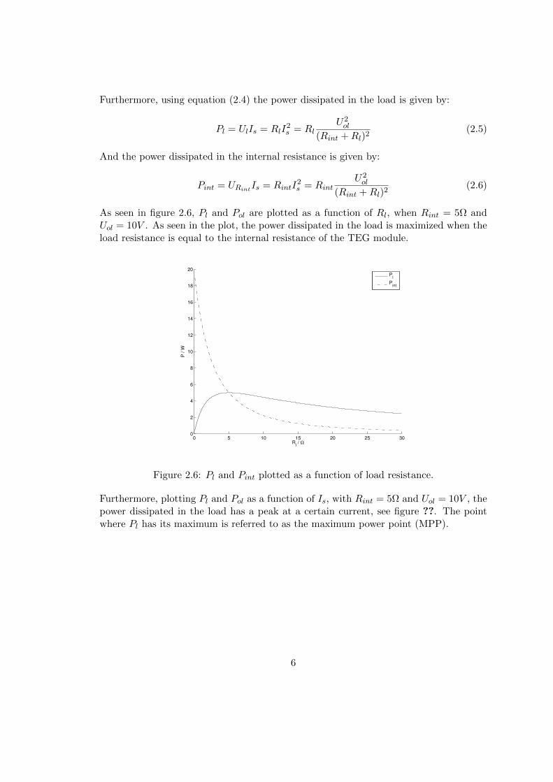
As seen in figure 2.6, Pl and Pol are plotted as a function of Rl, when Rint = 5Ω andUol = 10V . As seen in the plot, the power dissipated in the load is maximized when theload resistance is equal to the internal resistance of the TEG module.
0 5 10 15 20 25 300
2
4
6
8
10
12
14
16
18
20
Rl / Ω
P / W
Pl
Pint
Figure 2.6: Pl and Pint plotted as a function of load resistance.
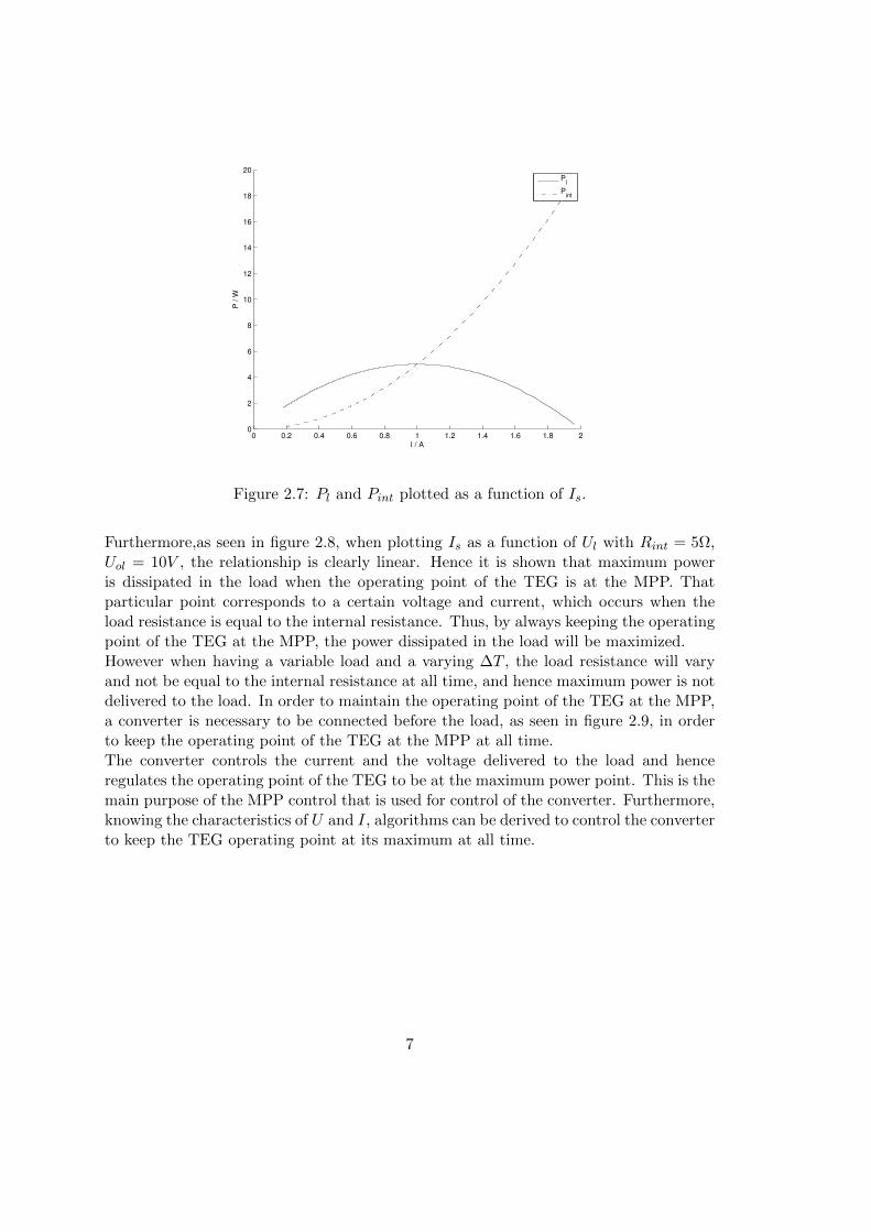
Furthermore, plotting Pl and Pol as a function of Is, with Rint = 5Ω and Uol = 10V , thepower dissipated in the load has a peak at a certain current, see figure ??. The pointwhere Pl has its maximum is referred to as the maximum power point (MPP).
6
0 0.2 0.4 0.6 0.8 1 1.2 1.4 1.6 1.8 20
2
4
6
8
10
12
14
16
18
20
I / A
P / W
Pl
Pint
Figure 2.7: Pl and Pint plotted as a function of Is.
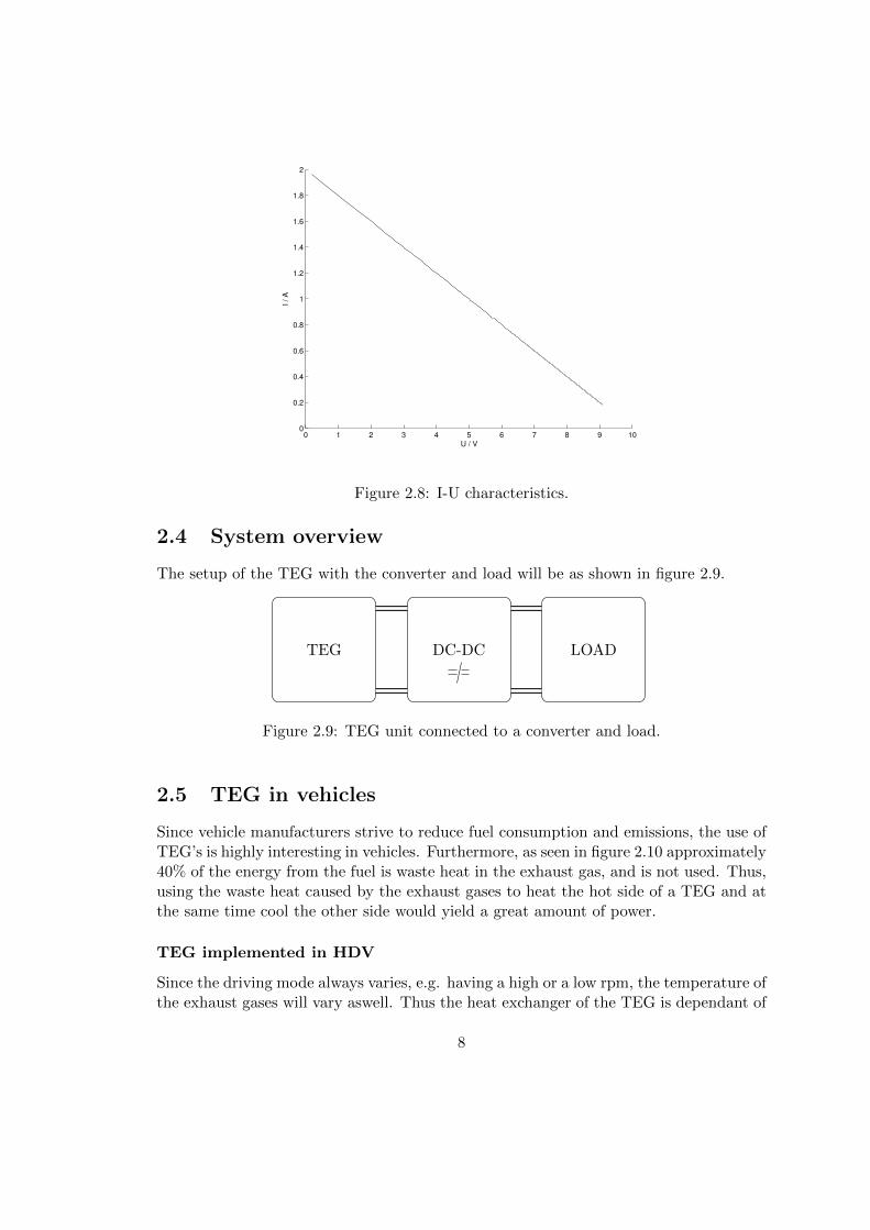
Furthermore,as seen in figure 2.8, when plotting Is as a function of Ul with Rint = 5Ω,Uol = 10V , the relationship is clearly linear. Hence it is shown that maximum poweris dissipated in the load when the operating point of the TEG is at the MPP. Thatparticular point corresponds to a certain voltage and current, which occurs when theload resistance is equal to the internal resistance. Thus, by always keeping the operatingpoint of the TEG at the MPP, the power dissipated in the load will be maximized.However when having a variable load and a varying ∆T , the load resistance will varyand not be equal to the internal resistance at all time, and hence maximum power is notdelivered to the load. In order to maintain the operating point of the TEG at the MPP,a converter is necessary to be connected before the load, as seen in figure 2.9, in orderto keep the operating point of the TEG at the MPP at all time.The converter controls the current and the voltage delivered to the load and henceregulates the operating point of the TEG to be at the maximum power point. This is themain purpose of the MPP control that is used for control of the converter. Furthermore,knowing the characteristics of U and I, algorithms can be derived to control the converterto keep the TEG operating point at its maximum at all time.
7
0 1 2 3 4 5 6 7 8 9 100
0.2
0.4
0.6
0.8
1
1.2
1.4
1.6
1.8
2
U / V
I / A
Figure 2.8: I-U characteristics.
2.4 System overview
The setup of the TEG with the converter and load will be as shown in figure 2.9.
TEG DC-DC LOAD
Figure 2.9: TEG unit connected to a converter and load.
2.5 TEG in vehicles
Since vehicle manufacturers strive to reduce fuel consumption and emissions, the use ofTEG’s is highly interesting in vehicles. Furthermore, as seen in figure 2.10 approximately40% of the energy from the fuel is waste heat in the exhaust gas, and is not used. Thus,using the waste heat caused by the exhaust gases to heat the hot side of a TEG and atthe same time cool the other side would yield a great amount of power.
TEG implemented in HDV
Since the driving mode always varies, e.g. having a high or a low rpm, the temperature ofthe exhaust gases will vary aswell. Thus the heat exchanger of the TEG is dependant of
8
25-5Automotive Applications of Thermoelectric Materials
!ere is an economic component to improving fuel e"ciency that has to be considered in thermoelec-tric generator (TEG) design. !ere are competing technologies to use waste heat for electric or mechani-cal power production. Some examples would be Rankin or Sterling cycle engines, steam engines, thermo-acoustic systems, and so on. !ermoelectric devices seem to have an edge because of their abil-ity to do direct heat-to-electric power conversion. It must also be considered that for automotive manu-facturers (and usually for customers), the lowest cost method for improving fuel economy is the best. !at means that the real competitor for TEG systems will continue to be all of the conventional improve-ments to engines, transmissions, and vehicles that improve their fuel economy. Fuel economy can be improved by many methods, such as enhanced fuel delivery systems, lower friction engines, improved transmissions with more speeds, better vehicle aerodynamics, hybrid propulsion systems, and many other vehicle engineering improvements. If these methods of fuel e"ciency improvement cost less than TEG systems, then the TEG systems will not be selected for automotive applications.
!ere are many reasons to incorporate TEGs in automotive systems. Some of those are as follows:
• Improve fuel e"ciency• Lower greenhouse gas (carbon dioxide) emissions• Support increased vehicle electri#cation• Simpler to implement than alternative waste heat recovery systems• Provide a “green” image for the vehicles
While all of these are good reasons to study TEGs, only improved fuel e"ciency is important enough to justify the cost of adding TEGs to cars and trucks.
An automotive TEG is a complete system integrated into a vehicle that uses vehicle waste heat energy and a cooling system to produce electricity for use on the vehicle. It should be noted that there is also the potential to produce the heat by burning fuel for the energy source in certain applications or some oper-ating conditions. !is integrated TEG system consists of several general components (see Figure 25.2):
1. A heat exchanger to take heat from the exhaust gases or engine coolant and deliver it to the hot side of the thermoelectric modules.
2. !ermoelectric modules with good conversion e"ciency (heat to electricity) in the available tem-perature range.
3. A heat exchanger to maintain the cold side of the thermoelectric modules by taking heat from the modules and radiating it to liquid coolant or to the air.
4. A housing to package the above components and to interface with the vehicle: mounting, exhaust connections, coolant connections, wiring, and so on.
5. An electrical power conditioning and interface unit to match the power output of the thermo-electric modules to the vehicle electrical system.
100%
40%Exhaust
gas
30%Coolant
5%Friction and
parasitic losses
25%Mobility andaccessories Co
mbu
stion
30%Engine
Vehicle operation
Gaso
line
FIGURE 25.1 Typical energy path for vehicles with gasoline fueled internal combustion engines.Figure 2.10: Typical energy path for a combustion engine[2].
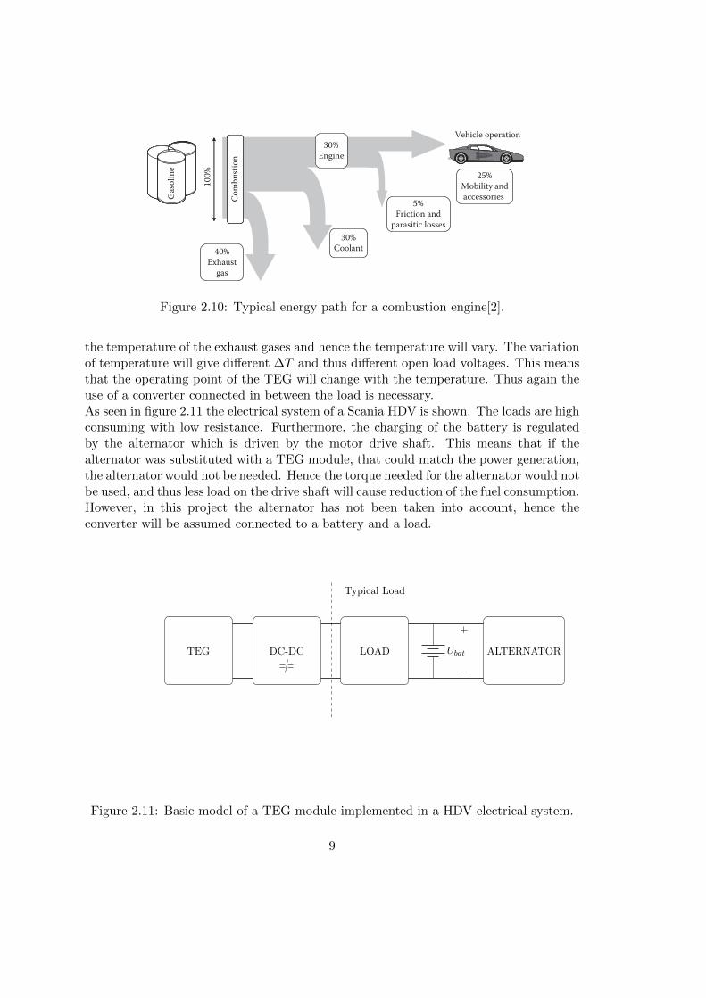
the temperature of the exhaust gases and hence the temperature will vary. The variationof temperature will give different ∆T and thus different open load voltages. This meansthat the operating point of the TEG will change with the temperature. Thus again theuse of a converter connected in between the load is necessary.As seen in figure 2.11 the electrical system of a Scania HDV is shown. The loads are highconsuming with low resistance. Furthermore, the charging of the battery is regulatedby the alternator which is driven by the motor drive shaft. This means that if thealternator was substituted with a TEG module, that could match the power generation,the alternator would not be needed. Hence the torque needed for the alternator would notbe used, and thus less load on the drive shaft will cause reduction of the fuel consumption.However, in this project the alternator has not been taken into account, hence theconverter will be assumed connected to a battery and a load.
TEG DC-DC LOAD ALTERNATOR
Typical Load
+
−
Ubat
Figure 2.11: Basic model of a TEG module implemented in a HDV electrical system.
9

TEG implemented in Hybrid HDV
A HDV driving style is often long haulage, which means that break regeneration willrarely occur. This means that the use of a TEG in a hybrid HDV could be beneficialsince extra electric power is generated from the waste heat recovery system.
The implementation of a TEG in a HDV could be done in two ways:
• Using one TEM for each cell in the hybrid battery, for charging.
• Using a TEG to charge the 24 V battery.
Both implementation techniques are possible, however further investigation is needed todetermine which one is the most beneficial.
10
Chapter 3
DC-DC Converters
3.1 DC-DC Converters
Several converter topologies can be used for maximum power harvesting from a TEG. Inthis project four converter topologies has been studied, the Buck-Boost, Cuk, SEPIC andfull bridge converter. However only the SEPIC converter was implemented. This wasdue to its simplicity and suitability, which is described in this chapter. Furthermore, thischapter describes the basic idea behind DC-DC converters and the different convertersthat has been studied.
3.2 Control of DC-DC converters
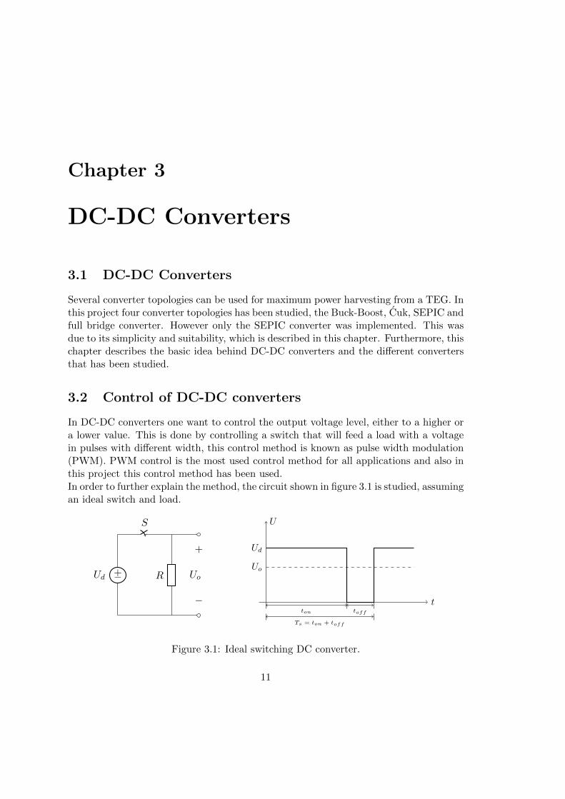
In DC-DC converters one want to control the output voltage level, either to a higher ora lower value. This is done by controlling a switch that will feed a load with a voltagein pulses with different width, this control method is known as pulse width modulation(PWM). PWM control is the most used control method for all applications and also inthis project this control method has been used.In order to further explain the method, the circuit shown in figure 3.1 is studied, assumingan ideal switch and load.
+−Ud
S
R
+
−
Uo
t
U
Uo
Ud
ton toff
Ts = ton + toff
Figure 3.1: Ideal switching DC converter.
11
The switch is conducting during ton and not conducting during toff , this is repeatedperiodically. Thus the entire switching period is given by
Ts = ton + toff (3.1)
And from figure 3.1 it is found that the duration that the switch is conducting is givenby
D =ton
ton + toff(3.2)
and is known as duty ratio (D).
As seen in figure 3.1, during ton the output voltage is equal to the input voltage andduring toff the output voltage is zero since the switch does not conduct.Furthermore, by controlling ton and toff , the average output voltage Uo is controlled.Thus, the average voltage Uo is dependent of the magnitude of Uin, ton and toff .This means that a higher ton gives a higher average output voltage, hence the averagevoltage is given by:
Uo =1
Ts
∫ ton
0Uin dt =
tonTs
Uin =ton
ton + toffUin (3.3)
The value of D gives the duration that the switch is conducting during one period inpercent, and changing D changes the output voltage. A higher D results in a higheroutput voltage, and lower D results in a lower voltage.This yields a transfer function for the example circuit:
Uo = DUin (3.4)
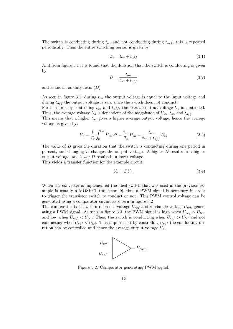
When the converter is implemented the ideal switch that was used in the previous ex-ample is usually a MOSFET-transistor [9], thus a PWM signal is necessary in orderto trigger the transistor switch to conduct or not. This PWM control voltage can begenerated using a comparator circuit as shown in figure 3.2 .The comparator is fed with a reference voltage Uref and a triangle voltage Utri, gener-ating a PWM signal. As seen in figure 3.3, the PWM signal is high when Uref > Utri,and low when Uref < Utri. Thus, the switch is conducting when Uref > Utri and notconducting when Uref < Utri. This implies that by controlling Uref the conducting du-ration can be controlled and hence the average output voltage Uo.
Utri
Uref
Upwm
Figure 3.2: Comparator generating PWM signal.
12

The frequency of the PWM signal is the same as the triangle voltage, hence by control-ling the frequency of the triangle voltage the PWM frequency is controlled. The PWMcontrol method is the most common way of controlling a DC-DC converter.However, it is necessary to mention that in modern power electronics the PWM controlvoltage is usually generated by a microprocessor. And in the implementation part ofthis thesis, a micro controller has been used to generate a PWM signal.
t
t
U
ton toff
Ts = ton + toff
On Off
Utri
Uref
Upwm
Figure 3.3: Generation of the PWM signal for the transistor switch.
3.3 The Buck-Boost Converter
The buck-boost converter shown in figure 3.4 is based on the buck and boost principle[9].As the name implies, the average output voltage can be higher or lower than the inputvoltage. The output average voltage and input voltage is given by:
Uo
Uin= − D
1−D(3.5)
Since the buck-boost is an inverting converter the ratio of average output voltage andinput voltage has a negative sign.
+−Uin
S
RlCL
D
+
−
Uo
Figure 3.4: Buck-Boost converter.
13
+−Uin RlC
iC
L
iL
+
−
Uo RlC
iC
L
iL
+
−
Uo
On-State Off-State
Figure 3.5: Equivalent circuit of the Buck-Boost converter during on- and off-state ofswitch.
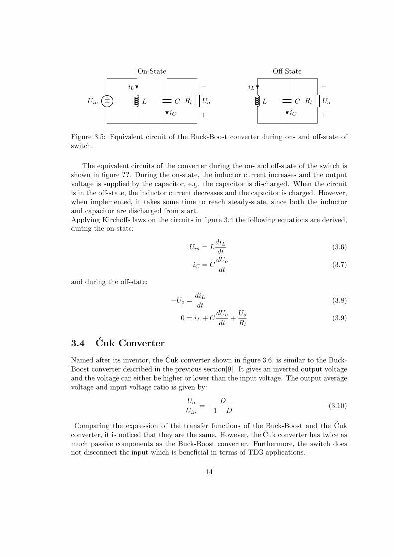
The equivalent circuits of the converter during the on- and off-state of the switch isshown in figure ??. During the on-state, the inductor current increases and the outputvoltage is supplied by the capacitor, e.g. the capacitor is discharged. When the circuitis in the off-state, the inductor current decreases and the capacitor is charged. However,when implemented, it takes some time to reach steady-state, since both the inductorand capacitor are discharged from start.Applying Kirchoffs laws on the circuits in figure 3.4 the following equations are derived,during the on-state:
Uin = LdiLdt
(3.6)
iC = CdUo
dt(3.7)
and during the off-state:
−Uo =diLdt
(3.8)
0 = iL + CdUo
dt+Uo
Rl(3.9)
3.4 Cuk Converter
Named after its inventor, the Cuk converter shown in figure 3.6, is similar to the Buck-Boost converter described in the previous section[9]. It gives an inverted output voltageand the voltage can either be higher or lower than the input voltage. The output averagevoltage and input voltage ratio is given by:
Uo
Uin= − D
1−D(3.10)
Comparing the expression of the transfer functions of the Buck-Boost and the Cukconverter, it is noticed that they are the same. However, the Cuk converter has twice asmuch passive components as the Buck-Boost converter. Furthermore, the switch doesnot disconnect the input which is beneficial in terms of TEG applications.
14
+−Uin
L1
S
C1
D
L2
C2 Rl
+
−
Uo
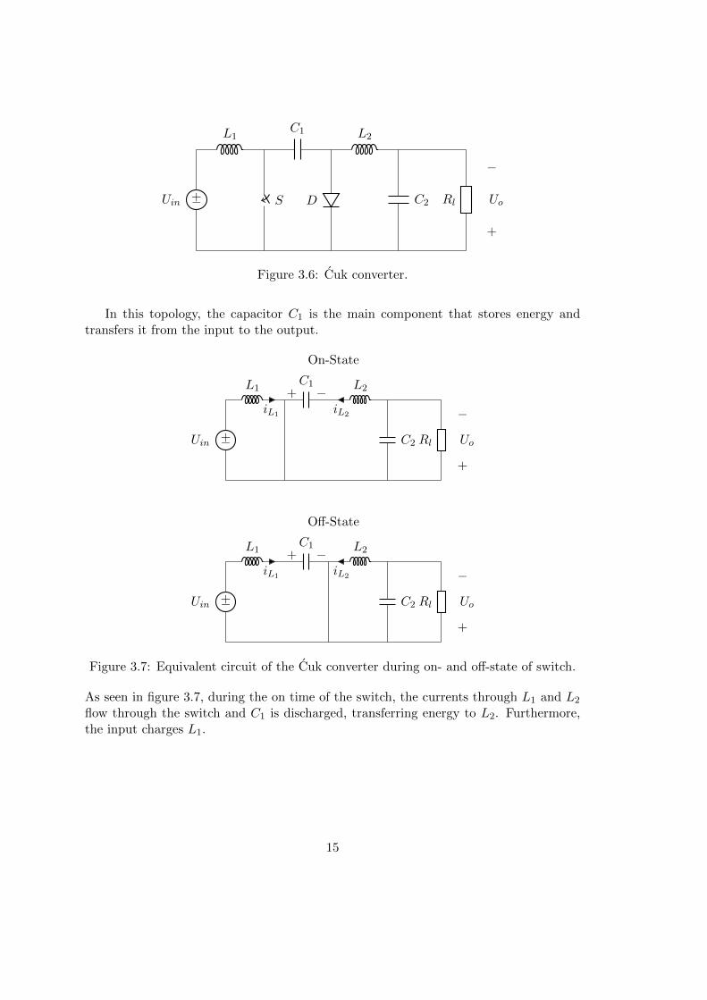
Figure 3.6: Cuk converter.
In this topology, the capacitor C1 is the main component that stores energy andtransfers it from the input to the output.
+−Uin
L1
iL1
C1+ − L2
iL2
C2 Rl
+
−
Uo
+−Uin
L1
iL1
C1+ − L2
iL2
C2 Rl
+
−
Uo
On-State
Off-State
Figure 3.7: Equivalent circuit of the Cuk converter during on- and off-state of switch.
As seen in figure 3.7, during the on time of the switch, the currents through L1 and L2
flow through the switch and C1 is discharged, transferring energy to L2. Furthermore,the input charges L1.
15
Hence, using Kirchoffs voltage law the following equations are derived during theon-state:
Uin = L1diL1
dt(3.11)
(Uin + Uo)− Uo = L2diL2
dt(3.12)
During the off time of the switch, the currents through inductor L1 and L2 flows throughthe diode. Furthermore, the capacitor C1 is charged with energy from the input and thecurrent stored in L1 and the inductor L2 feeds the output with its stored energy.Hence, using Kirchoffs voltage law the following equations are derived during the off-state:
(Uin + Uo)− Uin = L1diL1
dt(3.13)
Uo = L2diL2
dt(3.14)
3.5 SEPIC converter
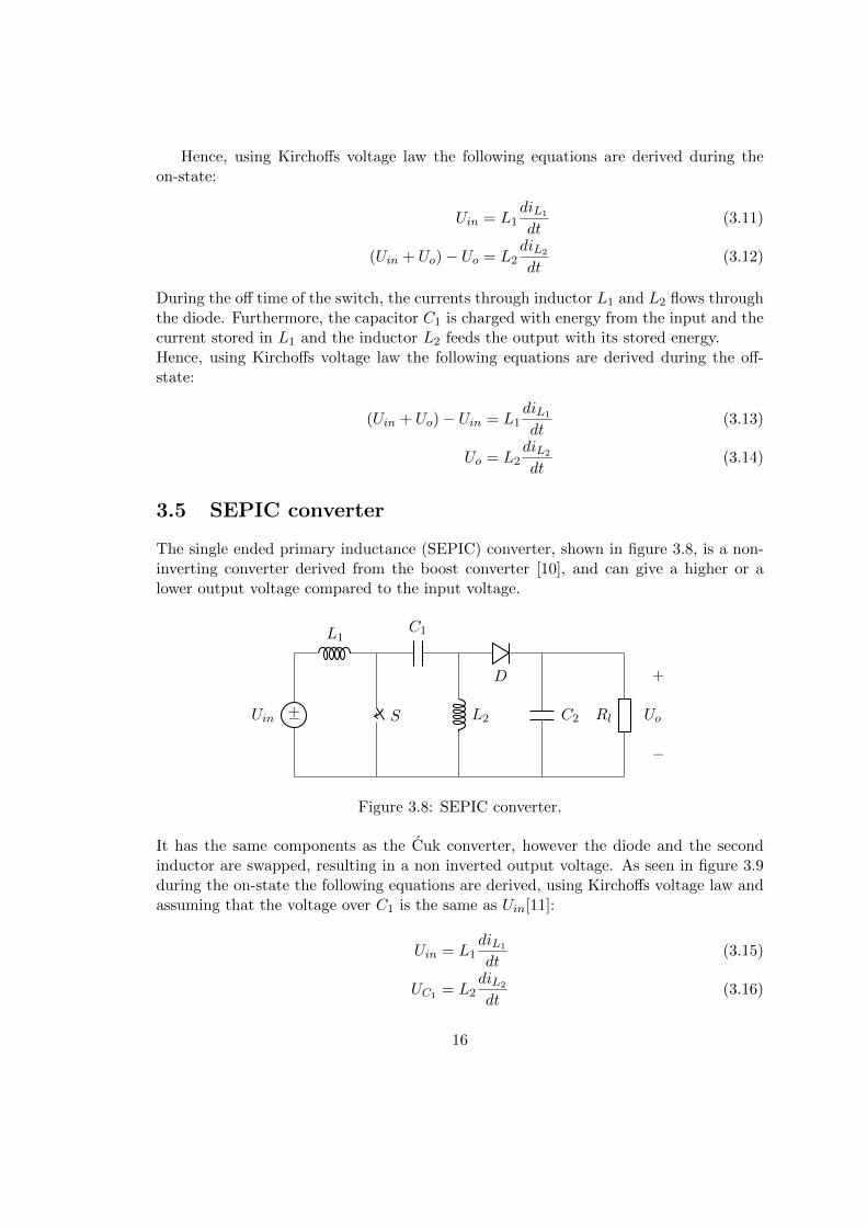
The single ended primary inductance (SEPIC) converter, shown in figure 3.8, is a non-inverting converter derived from the boost converter [10], and can give a higher or alower output voltage compared to the input voltage.
+−Uin
L1
S
C1
L2
D
C2 Rl
+
−
Uo
Figure 3.8: SEPIC converter.
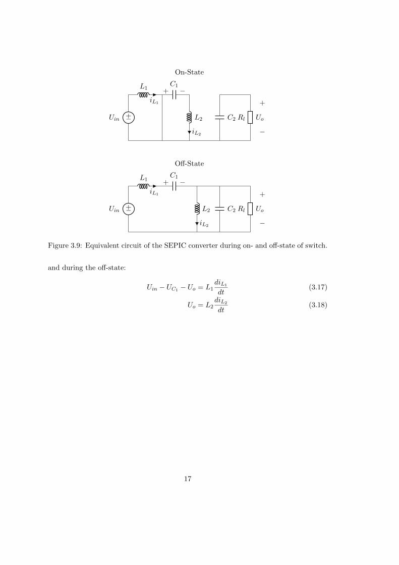
It has the same components as the Cuk converter, however the diode and the secondinductor are swapped, resulting in a non inverted output voltage. As seen in figure 3.9during the on-state the following equations are derived, using Kirchoffs voltage law andassuming that the voltage over C1 is the same as Uin[11]:
Uin = L1diL1
dt(3.15)
UC1 = L2diL2
dt(3.16)
16
+−Uin
L1
iL1
C1+ −
L2
iL2
C2 Rl
+
−
Uo
+−Uin
L1
iL1
L2
iL2
C1+ −
C2 Rl
+
−
Uo
On-State
Off-State
Figure 3.9: Equivalent circuit of the SEPIC converter during on- and off-state of switch.
and during the off-state:
Uin − UC1 − Uo = L1diL1
dt(3.17)
Uo = L2diL2
dt(3.18)
17

3.6 Full bridge converter
The full bridge converter shown in figure 3.10, is usually used to invert DC voltages,however with unipolar switching the converter can be used as a DC-DC converter. Fur-thermore the fullbridge converter is a bidirectional converter, meaning that it can transferenergy in both directions. This could be useful for future applications like heating theTE modules.
This converter type might be a better choice for usage with high power generation,due to it having no passive components. However, this type of converter might need afilter on its output if the voltage and current ripple needs to be in a certain range.
+−Uin
S
S
S
S
Rl
Figure 3.10: example caption
18
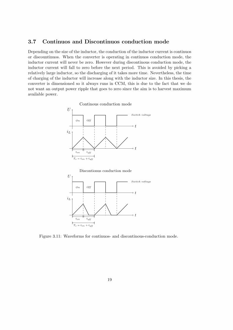
3.7 Continuos and Discontinuos conduction mode
Depending on the size of the inductor, the conduction of the inductor current is continuosor discountinuos. When the converter is operating in continuos conduction mode, theinductor current will never be zero. However during discontinous conduction mode, theinductor current will fall to zero before the next period. This is avoided by picking arelatively large inductor, so the discharging of it takes more time. Nevertheless, the timeof charging of the inductor will increase along with the inductor size. In this thesis, theconverter is dimensioned so it always runs in CCM, this is due to the fact that we donot want an output power ripple that goes to zero since the aim is to harvest maximumavailable power.
Discontionus conduction mode
t
t
U
iL
ton toff
Ts = ton + toff
On Off
Switch voltage
Continous conduction mode
t
t
U
iL
ton toff
Ts = ton + toff
On Off
Switch voltage
Figure 3.11: Waveforms for continuos- and discontinous-conduction mode.
19
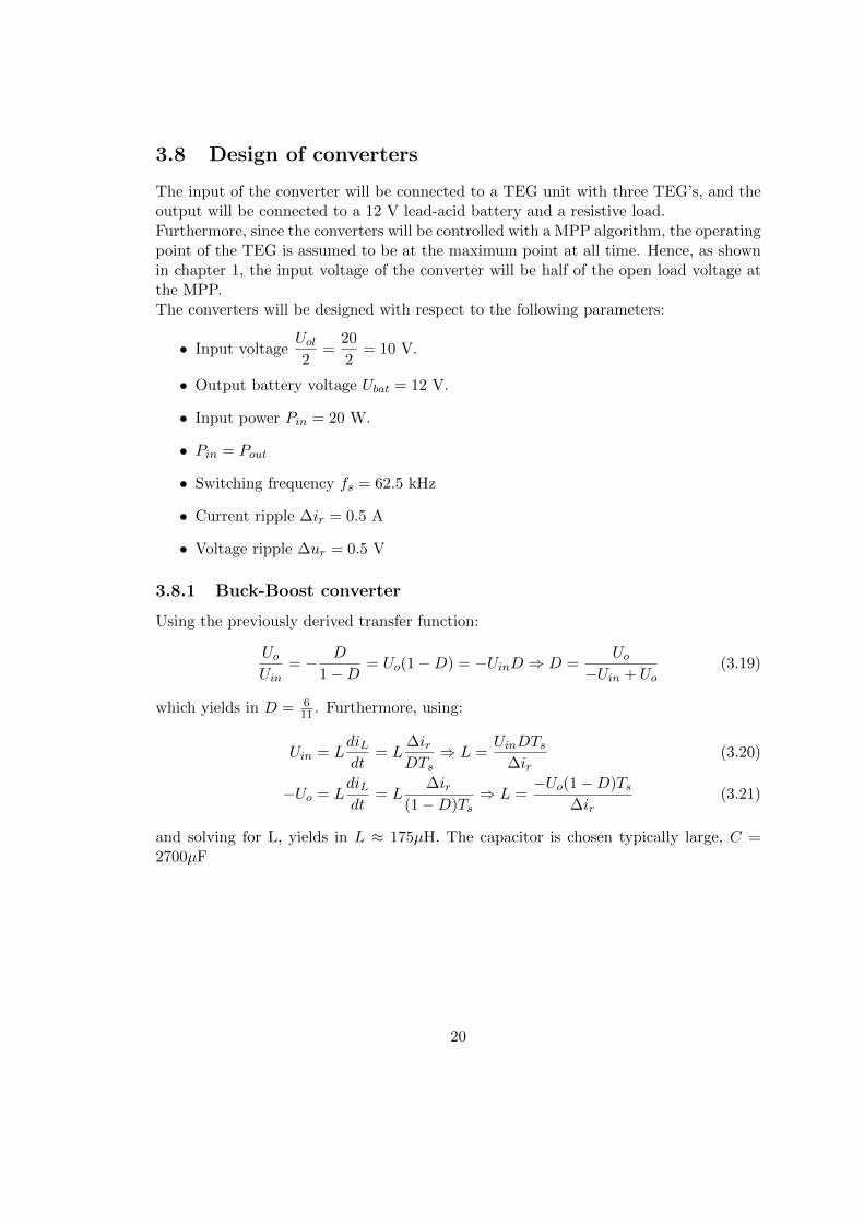
3.8 Design of converters
The input of the converter will be connected to a TEG unit with three TEG’s, and theoutput will be connected to a 12 V lead-acid battery and a resistive load.Furthermore, since the converters will be controlled with a MPP algorithm, the operatingpoint of the TEG is assumed to be at the maximum point at all time. Hence, as shownin chapter 1, the input voltage of the converter will be half of the open load voltage atthe MPP.The converters will be designed with respect to the following parameters:
• Input voltageUol
2=
20
2= 10 V.
• Output battery voltage Ubat = 12 V.
• Input power Pin = 20 W.
• Pin = Pout
• Switching frequency fs = 62.5 kHz
• Current ripple ∆ir = 0.5 A
• Voltage ripple ∆ur = 0.5 V
3.8.1 Buck-Boost converter
Using the previously derived transfer function:
Uo
Uin= − D
1−D= Uo(1−D) = −UinD ⇒ D =
Uo
−Uin + Uo(3.19)
which yields in D = 611 . Furthermore, using:
Uin = LdiLdt
= L∆irDTs
⇒ L =UinDTs
∆ir(3.20)
−Uo = LdiLdt
= L∆ir
(1−D)Ts⇒ L =
−Uo(1−D)Ts∆ir
(3.21)
and solving for L, yields in L ≈ 175µH. The capacitor is chosen typically large, C =2700µF
20
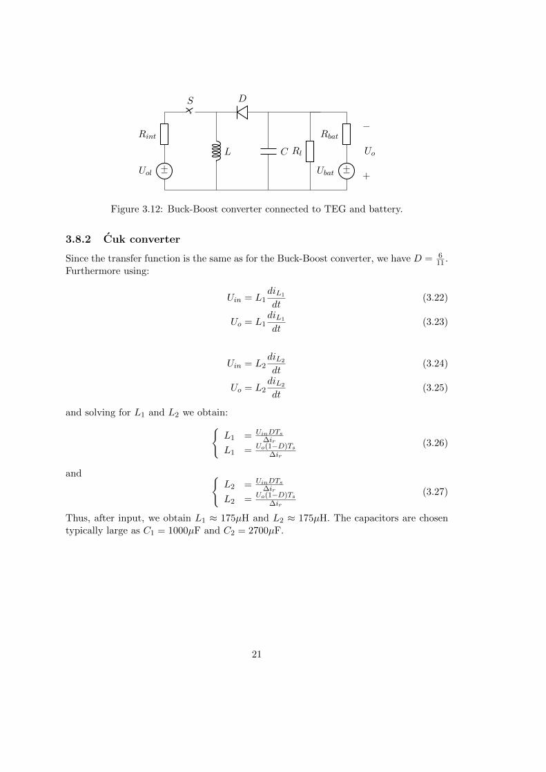
+−Uol
Rint
S
+−Ubat
Rbat
CL
D
Rl
+
−
Uo
Figure 3.12: Buck-Boost converter connected to TEG and battery.
3.8.2 Cuk converter
Since the transfer function is the same as for the Buck-Boost converter, we have D = 611 .
Furthermore using:
Uin = L1diL1
dt(3.22)
Uo = L1diL1
dt(3.23)
Uin = L2diL2
dt(3.24)
Uo = L2diL2
dt(3.25)
and solving for L1 and L2 we obtain:L1 = UinDTs
∆ir
L1 = Uo(1−D)Ts
∆ir
(3.26)
and L2 = UinDTs
∆ir
L2 = Uo(1−D)Ts
∆ir
(3.27)
Thus, after input, we obtain L1 ≈ 175µH and L2 ≈ 175µH. The capacitors are chosentypically large as C1 = 1000µF and C2 = 2700µF.
21
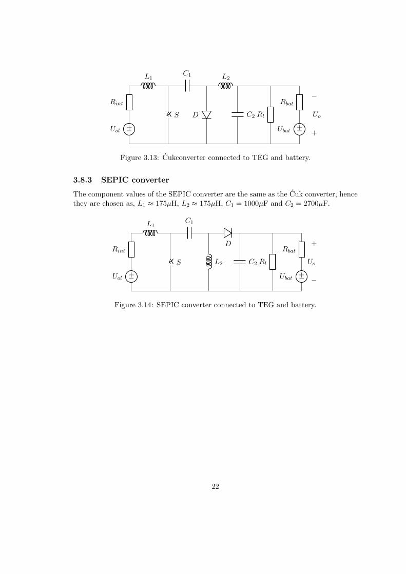
+−Uol
Rint
L1
S
C1
D
L2
C2
+−Ubat
Rbat
+
−
UoRl
Figure 3.13: Cukconverter connected to TEG and battery.
3.8.3 SEPIC converter
The component values of the SEPIC converter are the same as the Cuk converter, hencethey are chosen as, L1 ≈ 175µH, L2 ≈ 175µH, C1 = 1000µF and C2 = 2700µF.
+−Uol
Rint
L1
S
C1
L2
D
C2
+−Ubat
Rbat
+
−
UoRl
Figure 3.14: SEPIC converter connected to TEG and battery.
22
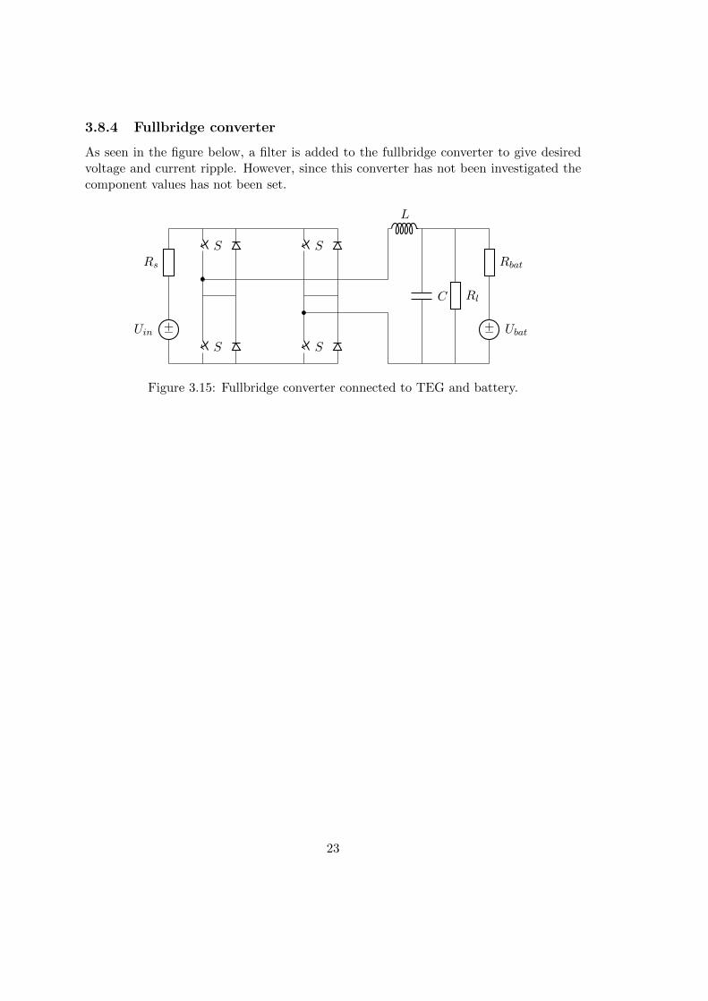
3.8.4 Fullbridge converter
As seen in the figure below, a filter is added to the fullbridge converter to give desiredvoltage and current ripple. However, since this converter has not been investigated thecomponent values has not been set.
+−Uin
Rs
S
S
S
S
L
C Rl
+−Ubat
Rbat
Figure 3.15: Fullbridge converter connected to TEG and battery.
23
3.9 Dimensioning of TEG module
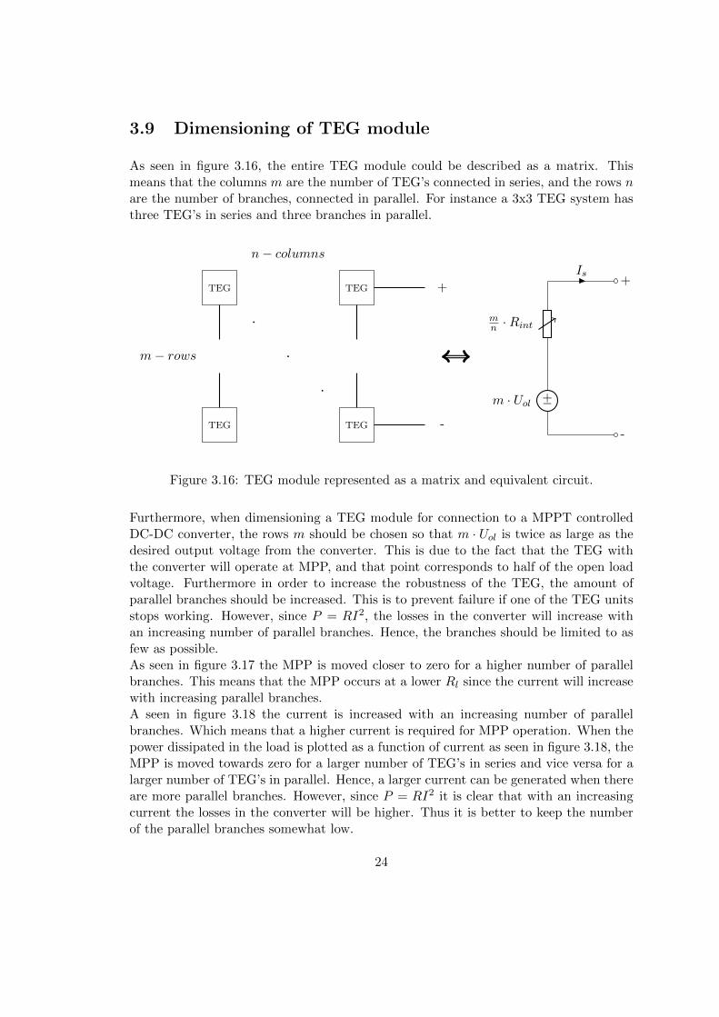
As seen in figure 3.16, the entire TEG module could be described as a matrix. Thismeans that the columns m are the number of TEG’s connected in series, and the rows nare the number of branches, connected in parallel. For instance a 3x3 TEG system hasthree TEG’s in series and three branches in parallel.
-
+
n− columns
m− rows
TEG TEG
TEGTEG
-
+−m · Uol
mn ·Rint
Is+
Figure 3.16: TEG module represented as a matrix and equivalent circuit.
Furthermore, when dimensioning a TEG module for connection to a MPPT controlledDC-DC converter, the rows m should be chosen so that m · Uol is twice as large as thedesired output voltage from the converter. This is due to the fact that the TEG withthe converter will operate at MPP, and that point corresponds to half of the open loadvoltage. Furthermore in order to increase the robustness of the TEG, the amount ofparallel branches should be increased. This is to prevent failure if one of the TEG unitsstops working. However, since P = RI2, the losses in the converter will increase withan increasing number of parallel branches. Hence, the branches should be limited to asfew as possible.As seen in figure 3.17 the MPP is moved closer to zero for a higher number of parallelbranches. This means that the MPP occurs at a lower Rl since the current will increasewith increasing parallel branches.A seen in figure 3.18 the current is increased with an increasing number of parallelbranches. Which means that a higher current is required for MPP operation. When thepower dissipated in the load is plotted as a function of current as seen in figure 3.18, theMPP is moved towards zero for a larger number of TEG’s in series and vice versa for alarger number of TEG’s in parallel. Hence, a larger current can be generated when thereare more parallel branches. However, since P = RI2 it is clear that with an increasingcurrent the losses in the converter will be higher. Thus it is better to keep the numberof the parallel branches somewhat low.
24
0 5 10 15 20 25 30 35 40 45 500
2
4
6
8
10
12
14
16
18
20
Rl / Ω
Pl /
W
1x1
2x1
1x2
3x1
1x3
Figure 3.17: The power dissipated in the load as a function of load resistance, for differentTEG unit setups.
3.10 Summary
After evaluating the converters, the SEPIC converter is determined to be most suitablefor implementation. This is due to the fact that it is non inverting and the TEG isconnected to the converter at all time, even when the switch is not conducting. This istaken into account since the aim is to harvest maximum power.Furthermore, due to the fact that the Buck-Boost converter will disconnect the TEGfrom the converter when the switch is not conducting, the Buck-Boost converter is ex-cluded from the simulations.In future applications, if the need of energy transfer in two directions is needed the full-bridge converter will be the best option. However, further investigation of the fullbridgeconverter is necessary.
25
0 1 2 3 4 5 60
2
4
6
8
10
12
14
16
I / A
Pl /
W
1x1
2x1
1x2
3x1
1x3
Figure 3.18: Power dissipated in the load, as a function of current.
26
Chapter 4
Maximum power point control
4.1 MPPT control
In order to set the duty ratio (D) to a value that sets the operating point of the TEGat the MPP, some feedback control is needed.There are several MPPT control algorithms that can be used for the control of a DC-DC converter. In this thesis the perturbe and observe (P&O) and the incrementalconductance (INC) algorithm have been investigated, since comparisons have shownthat these two have good dynamic responses [12], hence they are suitable for TEGapplications. Furthermore, [12] also shows an algorithm based on setting the operatingvoltage at half of the open load voltage, since this requires that the TEG is disconnectedfrom the converter, this algorithm is to some extent determined as inefficient since itdisconnects the TEG from the converter. Thus, this algorithm has not investigated.
4.1.1 Perturb and observe
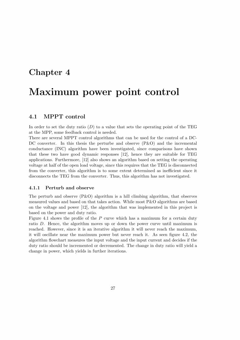
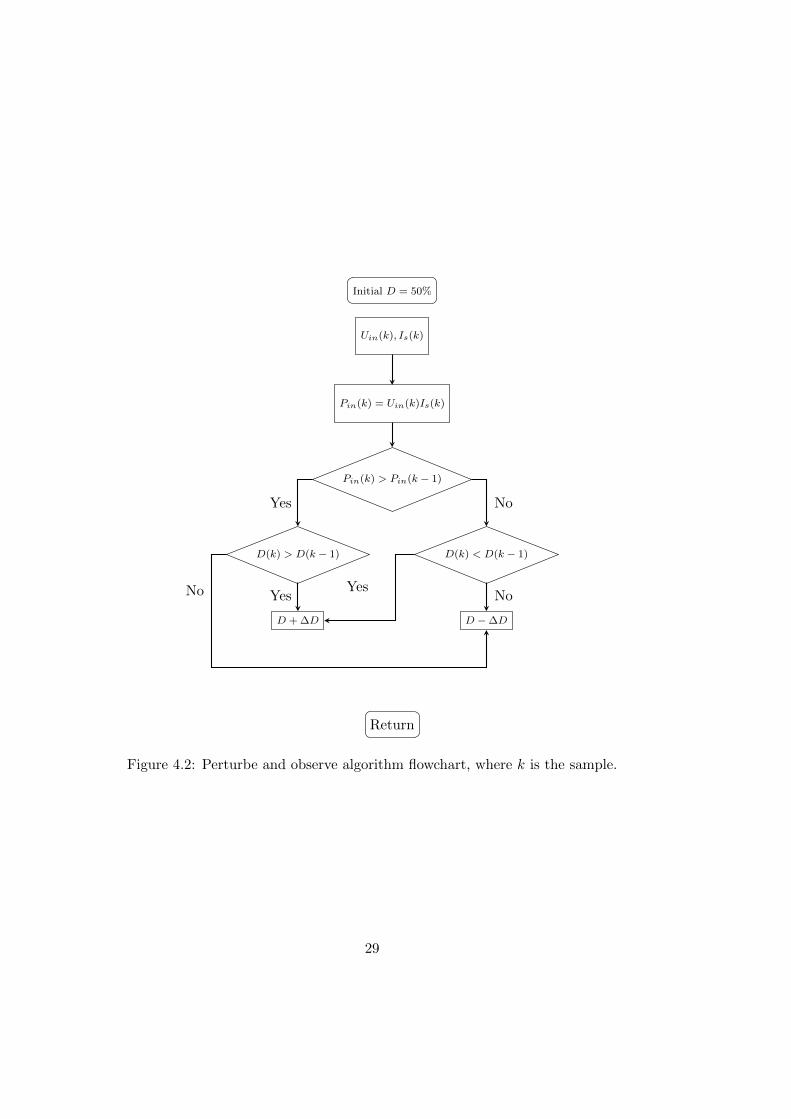
The perturb and observe (P&O) algorithm is a hill climbing algorithm, that observesmeasured values and based on that takes action. While most P&O algorithms are basedon the voltage and power [12], the algorithm that was implemented in this project isbased on the power and duty ratio.Figure 4.1 shows the profile of the P curve which has a maximum for a certain dutyratio D. Hence, the algorithm moves up or down the power curve until maximum isreached. However, since it is an iterative algorithm it will never reach the maximum,it will oscillate near the maximum power but never reach it. As seen figure 4.2, thealgorithm flowchart measures the input voltage and the input current and decides if theduty ratio should be incremented or decremented. The change in duty ratio will yield achange in power, which yields in further iterations.
27
D
P
Figure 4.1: Operation of perturb and observe control.
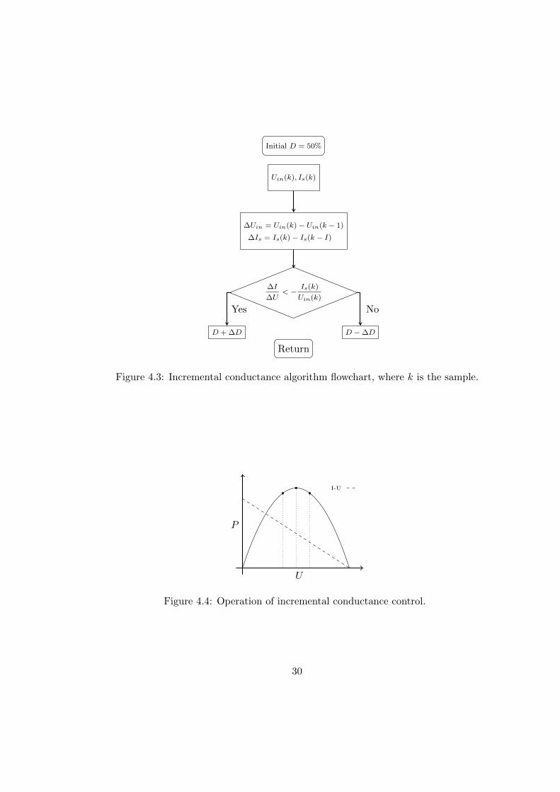
4.1.2 Incremental conductance
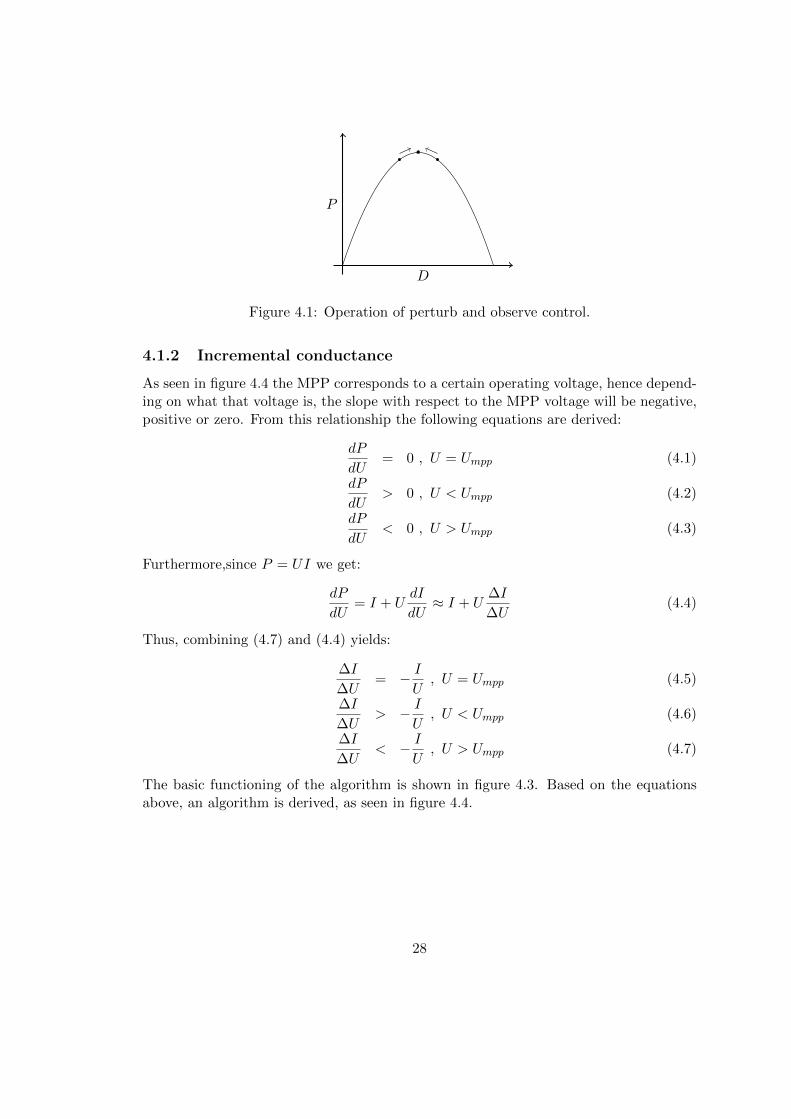
As seen in figure 4.4 the MPP corresponds to a certain operating voltage, hence depend-ing on what that voltage is, the slope with respect to the MPP voltage will be negative,positive or zero. From this relationship the following equations are derived:
dP
dU= 0 , U = Umpp (4.1)
dP
dU> 0 , U < Umpp (4.2)
dP
dU< 0 , U > Umpp (4.3)
Furthermore,since P = UI we get:
dP
dU= I + U
dI
dU≈ I + U
∆I
∆U(4.4)
Thus, combining (4.7) and (4.4) yields:
∆I
∆U= − I
U, U = Umpp (4.5)
∆I
∆U> − I
U, U < Umpp (4.6)
∆I
∆U< − I
U, U > Umpp (4.7)
The basic functioning of the algorithm is shown in figure 4.3. Based on the equationsabove, an algorithm is derived, as seen in figure 4.4.
28
Pin(k) = Uin(k)Is(k)
Uin(k), Is(k)
Pin(k) > Pin(k − 1)
D(k) > D(k − 1) D(k) < D(k − 1)
D + ∆D D − ∆D
Return
Initial D = 50%
NoYes
Yes NoYesNo
Figure 4.2: Perturbe and observe algorithm flowchart, where k is the sample.
29
Uin(k), Is(k)
∆Uin = Uin(k) − Uin(k − 1)
∆Is = Is(k) − Is(k − I)
∆I
∆U< −
Is(k)
Uin(k)
D + ∆D D − ∆D
Return
Initial D = 50%
NoYes
Figure 4.3: Incremental conductance algorithm flowchart, where k is the sample.
I-U
U
P
Figure 4.4: Operation of incremental conductance control.
30
Chapter 5
Simulation
5.1 Simulation
In order to analyse the TEG connected to a converter, simulation is necessary. However,since no TEG model was available a simulation model of the TEG was derived froma real TEG consisting of three TEM’s connected i series. The same setup was laterused to test with the converter. All the simulations were done in Matlab and Simulink’sSimscape and Sim Powersystems, the results and comparisons of the simulations thatwas made are presented in this chapter.
5.2 Modelling of the TEG
Previously no accurate model of the TEG was available for simulation, a model wasnecessary to be derived. The model was created using measurements of a real TEGthat consisted of three TEM’s. The TEM’s were connected in series and connected to avariable resistive load, as seen in figure 5.1, the actual test TEG is shown in AppendixA.Hence, using this circuit the characteristics of the TEM’s could be analysed, which laterwould be translated to a Simulink model in simulation environment.The TEM’s where sandwiched between two aluminium plates. Temperature sensorswhere placed in the aluminium plates both on the heated side and on the heat sinkfor temperature monitoring. The heat sink was cooled with water and the hot sidewas heated with a hot plate. The temperature of the hot side was held constant bymanual adjustements of the hot plate, this was a simple but not an accurate method oftemperature regulation. The temperature of the heat sink was regulated by adjustingthe flow of water in the cooler, also this method was not accurate.
31
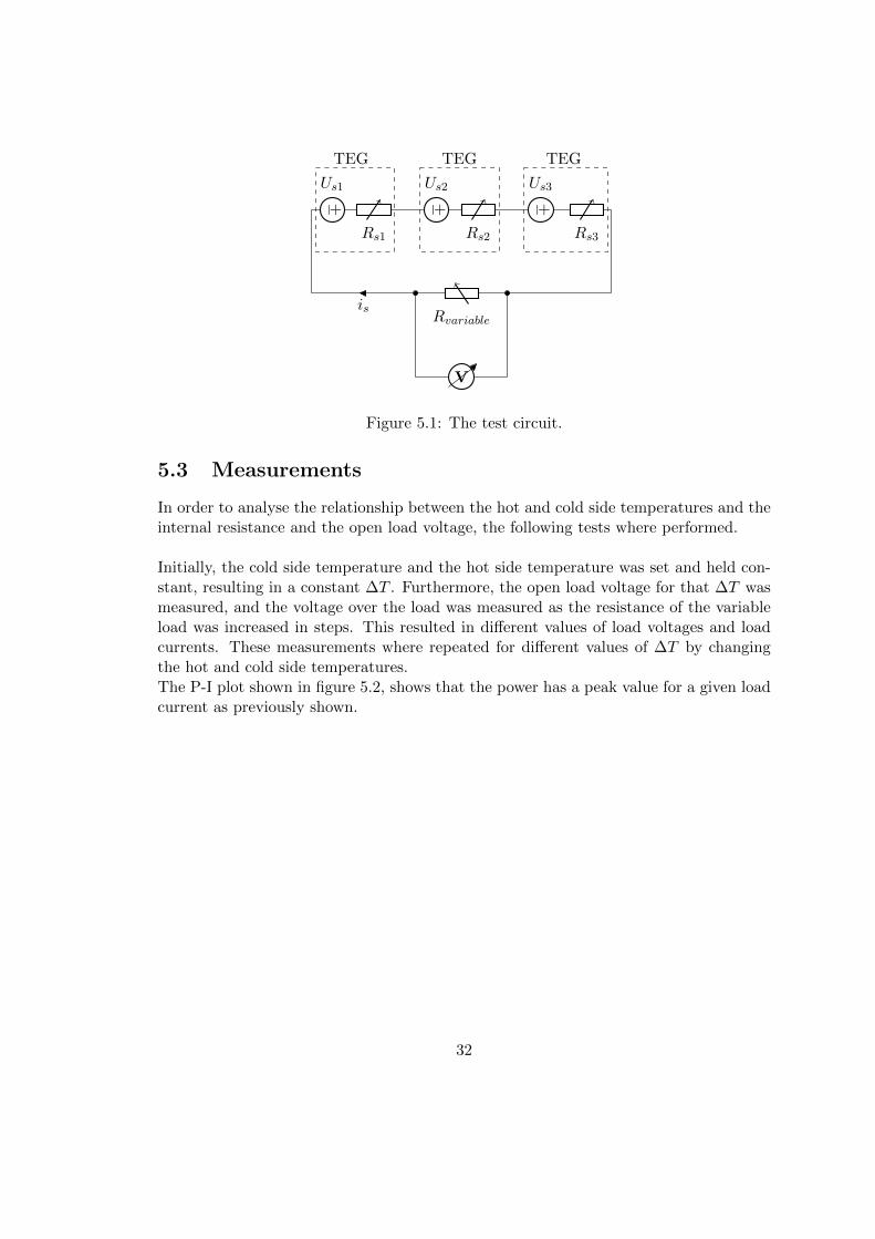
TEG TEG TEG
+−
Us1
Rs1
+−
Us2
Rs2
+−
Us3
Rs3
Rvariableis
V
Figure 5.1: The test circuit.
5.3 Measurements
In order to analyse the relationship between the hot and cold side temperatures and theinternal resistance and the open load voltage, the following tests where performed.
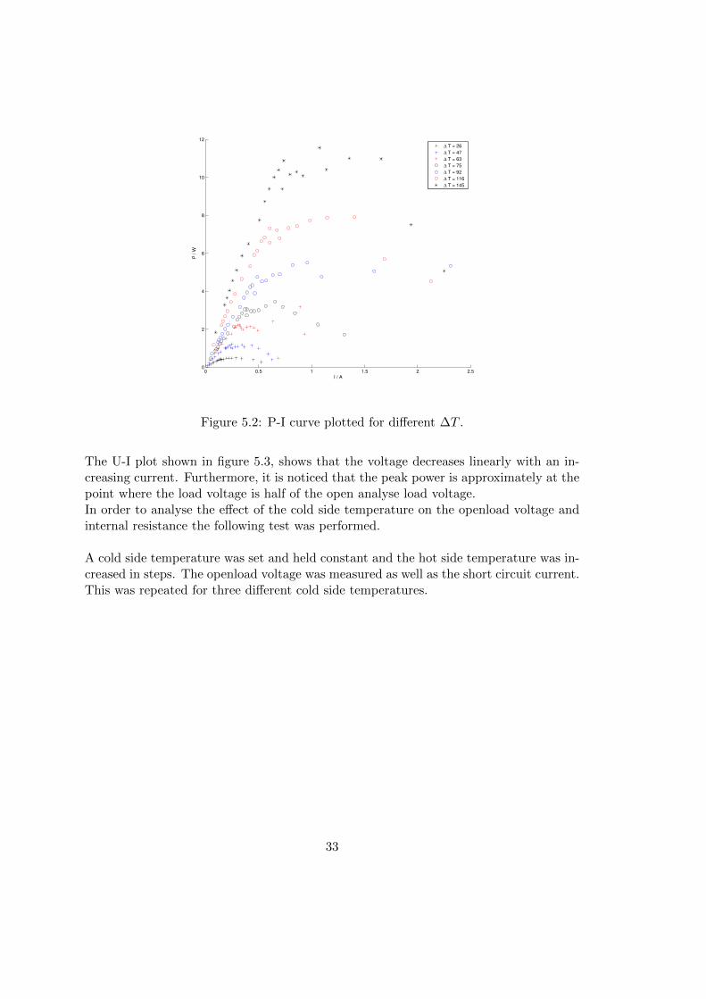
Initially, the cold side temperature and the hot side temperature was set and held con-stant, resulting in a constant ∆T . Furthermore, the open load voltage for that ∆T wasmeasured, and the voltage over the load was measured as the resistance of the variableload was increased in steps. This resulted in different values of load voltages and loadcurrents. These measurements where repeated for different values of ∆T by changingthe hot and cold side temperatures.The P-I plot shown in figure 5.2, shows that the power has a peak value for a given loadcurrent as previously shown.
32
0 0.5 1 1.5 2 2.50
2
4
6
8
10
12
I / A
P /
W
∆ T = 26
∆ T = 47
∆ T = 63
∆ T = 75
∆ T = 92
∆ T = 116
∆ T = 145
Figure 5.2: P-I curve plotted for different ∆T .
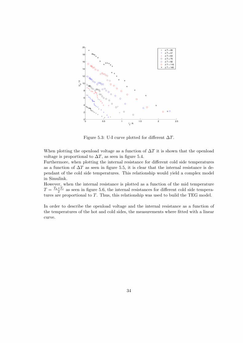
The U-I plot shown in figure 5.3, shows that the voltage decreases linearly with an in-creasing current. Furthermore, it is noticed that the peak power is approximately at thepoint where the load voltage is half of the open analyse load voltage.In order to analyse the effect of the cold side temperature on the openload voltage andinternal resistance the following test was performed.
A cold side temperature was set and held constant and the hot side temperature was in-creased in steps. The openload voltage was measured as well as the short circuit current.This was repeated for three different cold side temperatures.
33
0 0.5 1 1.5 2 2.50
2
4
6
8
10
12
14
16
18
20
Is / A
Uol /
V
∆ T = 26
∆ T = 47
∆ T = 63
∆ T = 75
∆ T = 92
∆ T = 116
∆ T = 145
Figure 5.3: U-I curve plotted for different ∆T .
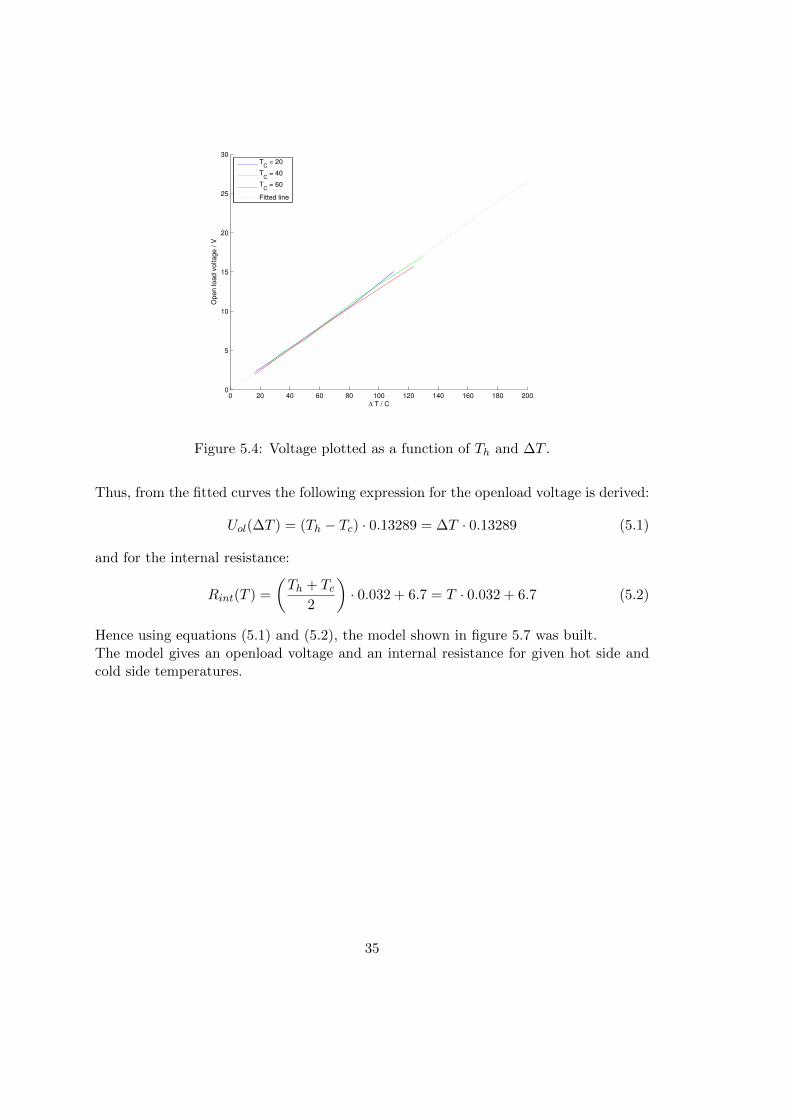
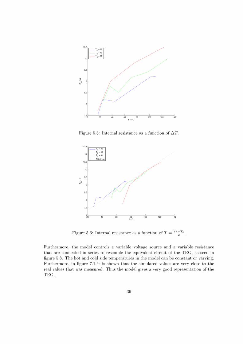
When plotting the openload voltage as a function of ∆T it is shown that the openloadvoltage is proportional to ∆T , as seen in figure 5.4.Furthermore, when plotting the internal resistance for different cold side temperaturesas a function of ∆T as seen in figure 5.5, it is clear that the internal resistance is de-pendant of the cold side temperatures. This relationship would yield a complex modelin Simulink.However, when the internal resistance is plotted as a function of the mid temperatureT = Th+Tc
2 as seen in figure 5.6, the internal resistances for different cold side tempera-tures are proportional to T . Thus, this relationship was used to build the TEG model.
In order to describe the openload voltage and the internal resistance as a function ofthe temperatures of the hot and cold sides, the measurements where fitted with a linearcurve.
34
0 20 40 60 80 100 120 140 160 180 2000
5
10
15
20
25
30
∆ T / C
Open load v
oltage / V
T
C = 20
TC
= 40
TC
= 60
Fitted line
Figure 5.4: Voltage plotted as a function of Th and ∆T .
Thus, from the fitted curves the following expression for the openload voltage is derived:
Uol(∆T ) = (Th − Tc) · 0.13289 = ∆T · 0.13289 (5.1)
and for the internal resistance:
Rint(T ) =
(Th + Tc
2
)· 0.032 + 6.7 = T · 0.032 + 6.7 (5.2)
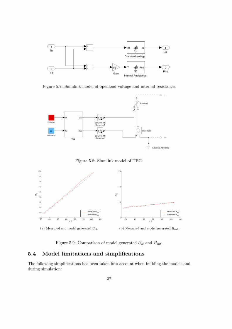
Hence using equations (5.1) and (5.2), the model shown in figure 5.7 was built.The model gives an openload voltage and an internal resistance for given hot side andcold side temperatures.
35
0 20 40 60 80 100 120 1407.5
8
8.5
9
9.5
10
10.5
∆ T / C
Rin
t / Ω
TC
= 20
TC
= 40
TC
= 60
Figure 5.5: Internal resistance as a function of ∆T .
20 40 60 80 100 120 1407
7.5
8
8.5
9
9.5
10
10.5
11
11.5
T / C
Rin
t / Ω
TC
= 20
TC
= 40
TC
= 60
Fitted line
Figure 5.6: Internal resistance as a function of T = Th+Tc
2 .
Furthermore, the model controls a variable voltage source and a variable resistancethat are connected in series to resemble the equivalent circuit of the TEG, as seen infigure 5.8. The hot and cold side temperatures in the model can be constant or varying.Furthermore, in figure 7.1 it is shown that the simulated values are very close to thereal values that was measured. Thus the model gives a very good representation of theTEG.
36
Rint
2
Uol
1
Openload Voltage
dT U
fcn
Internal Resistance
T Rint
fcnGain
1/2
Tc
2
Th
1
Figure 5.7: Simulink model of openload voltage and internal resistance.
−
+
Uopenload
TEG
Th
Tc
Uol
Rint
Simulink−PS
Converter2
S PS
Simulink−PS
Converter1
S PS
Rinternal
−+P
S
Hottemp
140
Electrical Reference
Coldtemp
20
Figure 5.8: Simulink model of TEG.
20 40 60 80 100 120 140 1602
4
6
8
10
12
14
16
18
20
∆ T
Uol
Measured Uol
Simulated Uol
(a) Measured and model generated Uol.
20 40 60 80 100 120 1405
10
15
20
∆ T
Rin
t
Measured Rint
Simulated Rint
(b) Measured and model generated Rint.
Figure 5.9: Comparison of model generated Uol and Rint.
5.4 Model limitations and simplifications
The following simplifications has been taken into account when building the models andduring simulation:
37
• The TEG models voltage and resistance is assumed to be linear for any tempera-ture. This means that very high temperatures result in very high power output,where in reality the TEG may be over its maximum temperature and break down.
• It is assumed that all TEGs have identical characteristics. However, in realitysmall differences can be expected.
• It is assumed that every TEG is exposed to exactly the same temperatures on thehot and cold side.
• The model does not consider that stealing energy from the gas, the hot side of theTEG and any material in between, would lower the temperature on the hot side,and increase the temperature on the cold side.
• The efficiency maps doesn’t consider any transient behaviour of the converters,and the efficiency between the measured points is linearly interpolated.
• The look-up table for EGR-gas temperature doesn’t cover every case in the drivecycles. Temperature data outside of the map is extrapolated.
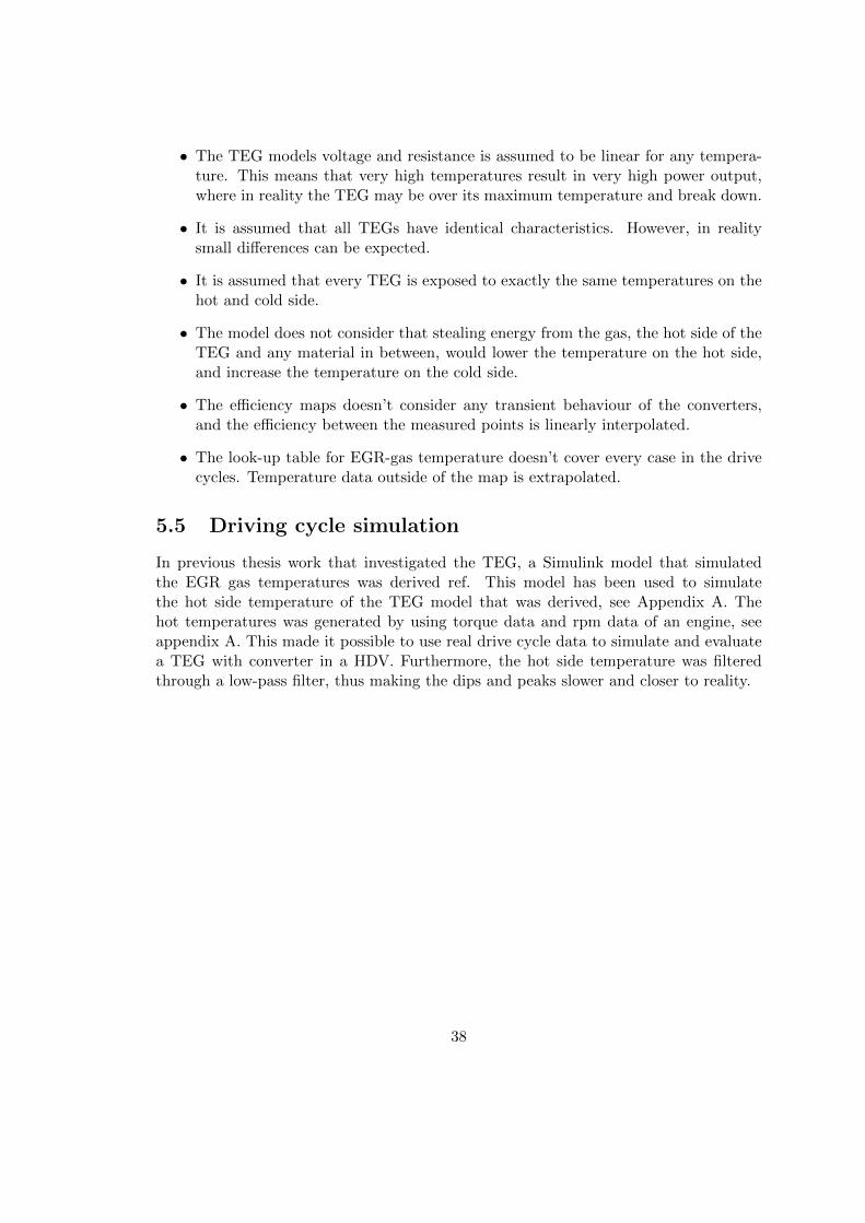
5.5 Driving cycle simulation
In previous thesis work that investigated the TEG, a Simulink model that simulatedthe EGR gas temperatures was derived ref. This model has been used to simulatethe hot side temperature of the TEG model that was derived, see Appendix A. Thehot temperatures was generated by using torque data and rpm data of an engine, seeappendix A. This made it possible to use real drive cycle data to simulate and evaluatea TEG with converter in a HDV. Furthermore, the hot side temperature was filteredthrough a low-pass filter, thus making the dips and peaks slower and closer to reality.
38

5.6 Simulation settings
The simulations where run in Simulink, Simscape and Sim Power Systems. Since SimPower Systems does not have a variable resistor, the model of the converters where builtin Simscape. However, the battery model from Sim Power systems was used in themodel, also this model was modified in order to be able to run with Simscape.
Furthermore, in order to generate an accurate PWM signal, the maximum step lengthwas set to 1−6 and the solver was set to ode23t.This yielded an accurate PWM signal, however the simulations where run at a veryslow speed. Furthermore, since a 2.5 h driving cycle of a HDV was going to be used togenerate the temperature of the hot side of a TEG. An efficiency mapping was made tomake it possible to use the hot temperature generated in a real driving cycle to evaluatethe efficiency of the converter. See Appendix B for the complete simulation models.
39
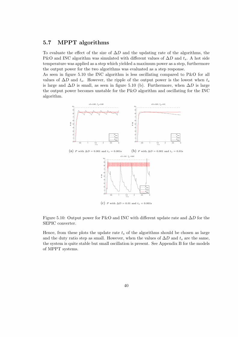
5.7 MPPT algorithms
To evaluate the effect of the size of ∆D and the updating rate of the algorithms, theP&O and INC algorithm was simulated with different values of ∆D and ts. A hot sidetemperature was applied as a step which yielded a maximum power as a step, furthermorethe output power for the two algorithms was evaluated as a step response.As seen in figure 5.10 the INC algorithm is less oscillating compared to P&O for allvalues of ∆D and ts. However, the ripple of the output power is the lowest when tsis large and ∆D is small, as seen in figure 5.10 (b). Furthermore, when ∆D is largethe output power becomes unstable for the P&O algorithm and oscillating for the INCalgorithm.
0.5 1 1.5 2 2.5 30
1
2
3
4
5
6
7
8
9
10
t / s
P /
W
∆ D = 0.001 , TD
= 0.001
Pmax
PP&O
PINC
(a) P with ∆D = 0.001 and ts = 0.001s
0.5 1 1.5 2 2.5 30
1
2
3
4
5
6
7
8
9
10
t / s
P /
W
∆ D = 0.001 , TD
= 0.01
Pmax
PP&O
PINC
(b) P with ∆D = 0.001 and ts = 0.01s
0.5 1 1.5 2 2.5 30
1
2
3
4
5
6
7
8
9
10
t / s
P /
W
∆ D = 0.01 , TD
= 0.001
Pmax
PP&O
PINC
(c) P with ∆D = 0.01 and ts = 0.001s
Figure 5.10: Output power for P&O and INC with different update rate and ∆D for theSEPIC converter.
Hence, from these plots the update rate ts of the algorithms should be chosen as largeand the duty ratio step as small. However, when the values of ∆D and ts are the same,the system is quite stable but small oscillation is present. See Appendix B for the modelsof MPPT systems.
40
5.8 Efficiency mapping
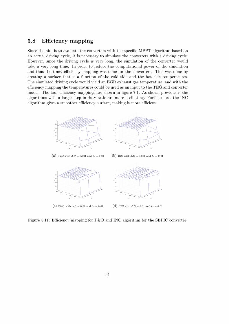
Since the aim is to evaluate the converters with the specific MPPT algorithm based onan actual driving cycle, it is necessary to simulate the converters with a driving cycle.However, since the driving cycle is very long, the simulation of the converter wouldtake a very long time. In order to reduce the computational power of the simulationand thus the time, efficiency mapping was done for the converters. This was done bycreating a surface that is a function of the cold side and the hot side temperatures.The simulated driving cycle would yield an EGR exhaust gas temperature, and with theefficiency mapping the temperatures could be used as an input to the TEG and convertermodel. The four efficiency mappings are shown in figure 7.1. As shown previously, thealgorithms with a larger step in duty ratio are more oscillating. Furthermore, the INCalgorithm gives a smoother efficiency surface, making it more efficient.
10
20
30
40
50
60
70
80
100
200
300
400
500
600
0
0.2
0.4
0.6
0.8
1
TcTh
η
(a) P&O with ∆D = 0.001 and ts = 0.01
10
20
30
40
50
60
70
80
100
200
300
400
500
600
0
0.2
0.4
0.6
0.8
1
TcTh
η
(b) INC with ∆D = 0.001 and ts = 0.01
10
20
30
40
50
60
70
80
100
200
300
400
500
600
0
0.2
0.4
0.6
0.8
1
TcTh
η
(c) P&O with ∆D = 0.01 and ts = 0.01
10
20
30
40
50
60
70
80
100
200
300
400
500
600
0
0.2
0.4
0.6
0.8
1
TcTh
η
(d) INC with ∆D = 0.01 and ts = 0.01
Figure 5.11: Efficiency mapping for P&O and INC algorithm for the SEPIC converter.
41

42
Chapter 6
Implementation
In order to analyse the TEG with the SEPIC converter, a SEPIC converter with MPPTcontrol was constructed. The aim was only to study the operation, thus it was notoptimised in terms of components and control.For the control of the converter an Arduino UNO micro controller was used, mainly forits easy implementation and usage.
6.1 Current sensor
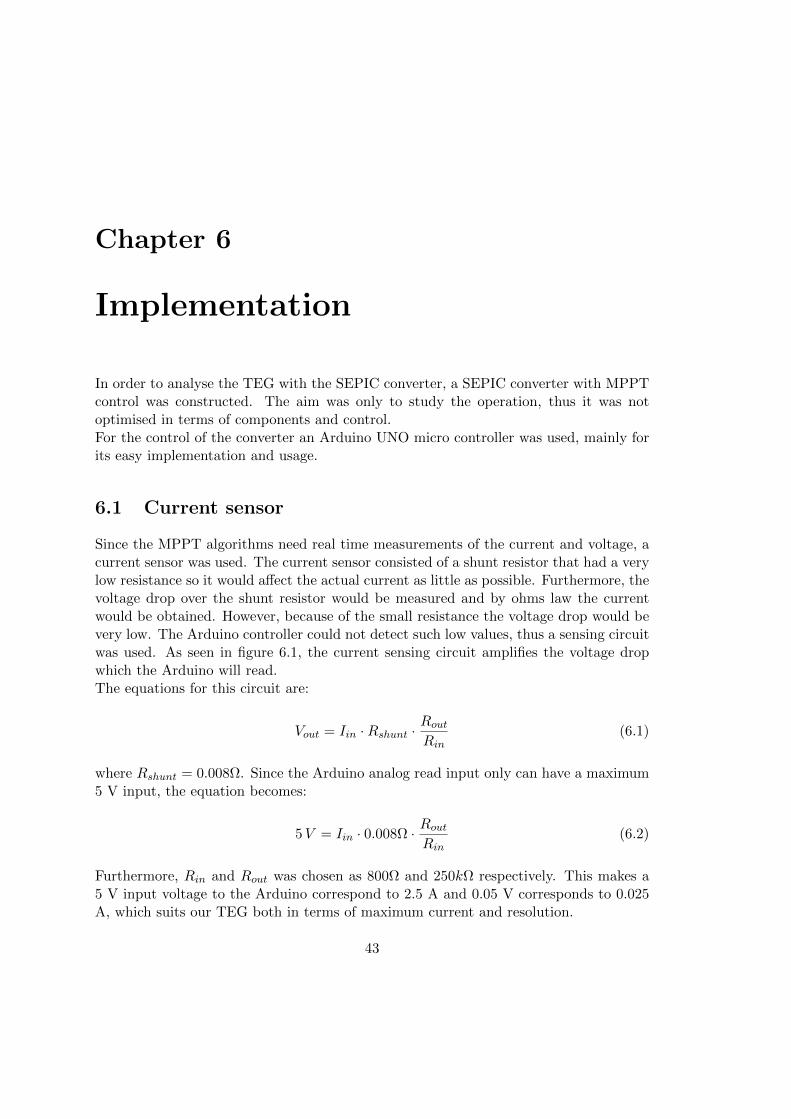
Since the MPPT algorithms need real time measurements of the current and voltage, acurrent sensor was used. The current sensor consisted of a shunt resistor that had a verylow resistance so it would affect the actual current as little as possible. Furthermore, thevoltage drop over the shunt resistor would be measured and by ohms law the currentwould be obtained. However, because of the small resistance the voltage drop would bevery low. The Arduino controller could not detect such low values, thus a sensing circuitwas used. As seen in figure 6.1, the current sensing circuit amplifies the voltage dropwhich the Arduino will read.The equations for this circuit are:
Vout = Iin ·Rshunt ·Rout
Rin(6.1)
where Rshunt = 0.008Ω. Since the Arduino analog read input only can have a maximum5 V input, the equation becomes:
5V = Iin · 0.008Ω · Rout
Rin(6.2)
Furthermore, Rin and Rout was chosen as 800Ω and 250kΩ respectively. This makes a5 V input voltage to the Arduino correspond to 2.5 A and 0.05 V corresponds to 0.025A, which suits our TEG both in terms of maximum current and resolution.
43
−
+
UDD = 5V
Rin
Rshunt
Rout
Uout
iin
Figure 6.1: Current sensing circuit.
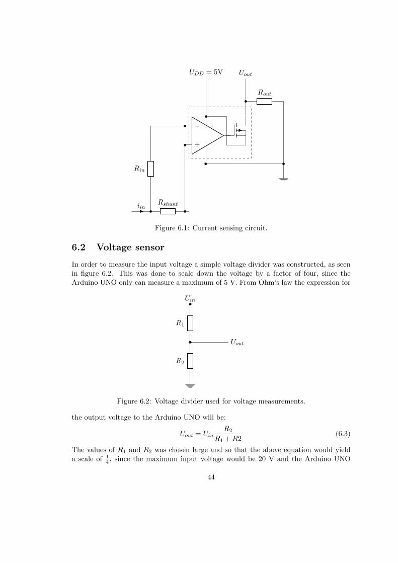
6.2 Voltage sensor
In order to measure the input voltage a simple voltage divider was constructed, as seenin figure 6.2. This was done to scale down the voltage by a factor of four, since theArduino UNO only can measure a maximum of 5 V. From Ohm’s law the expression for
R2
R1
Uout
Uin
Figure 6.2: Voltage divider used for voltage measurements.
the output voltage to the Arduino UNO will be:
Uout = UinR2
R1 +R2(6.3)
The values of R1 and R2 was chosen large and so that the above equation would yielda scale of 1
4 , since the maximum input voltage would be 20 V and the Arduino UNO
44
maximum analog read is 5 V.Furthermore, another voltage divider was constructed to measure the voltage of thebattery on the output, this was done to monitor the battery voltage and prevent over-charging. The scale for the battery voltage was set to be 1
3 , to prevent over voltage tobe fed to the Arduino.
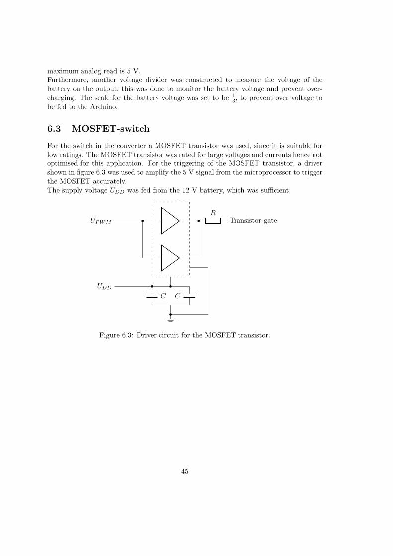
6.3 MOSFET-switch
For the switch in the converter a MOSFET transistor was used, since it is suitable forlow ratings. The MOSFET transistor was rated for large voltages and currents hence notoptimised for this application. For the triggering of the MOSFET transistor, a drivershown in figure 6.3 was used to amplify the 5 V signal from the microprocessor to triggerthe MOSFET accurately.The supply voltage UDD was fed from the 12 V battery, which was sufficient.
RTransistor gateUPWM
CC
UDD
Figure 6.3: Driver circuit for the MOSFET transistor.
45
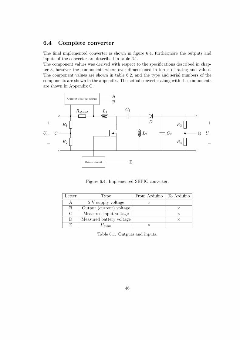
6.4 Complete converter
The final implemented converter is shown in figure 6.4, furthermore the outputs andinputs of the converter are described in table 6.1.The component values was derived with respect to the specifications described in chap-ter 3, however the components where over dimensioned in terms of rating and values.The component values are shown in table 6.2, and the type and serial numbers of thecomponents are shown in the appendix. The actual converter along with the componentsare shown in Appendix C.
R2
R1
C D
Rshunt L1C1
L2
D
C2
R4
R3
B
A
+
−
Uin
+
−
Uo
E
Current sensing circuit
Driver circuit
Figure 6.4: Implemented SEPIC converter.
Letter Type From Arduino To Arduino
A 5 V supply voltage ×B Output (current) voltage ×C Measured input voltage ×D Measured battery voltage ×E Upwm ×
Table 6.1: Outputs and inputs.
46
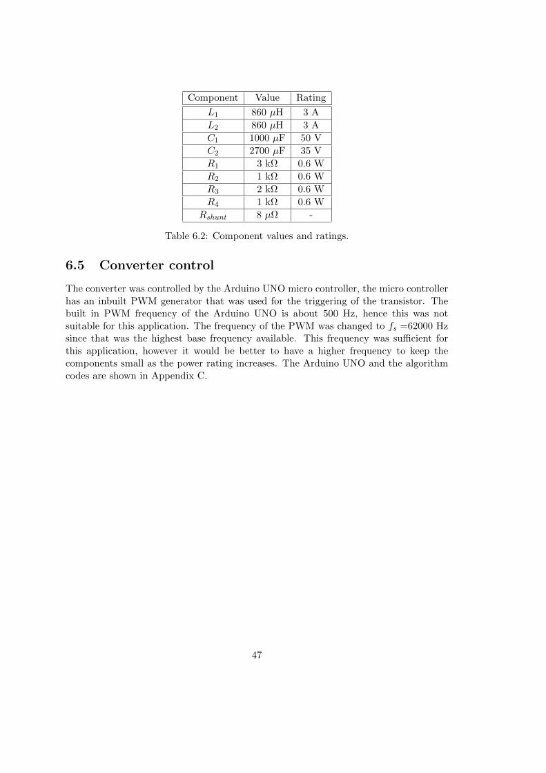
Component Value Rating
L1 860 µH 3 A
L2 860 µH 3 A
C1 1000 µF 50 V
C2 2700 µF 35 V
R1 3 kΩ 0.6 W
R2 1 kΩ 0.6 W
R3 2 kΩ 0.6 W
R4 1 kΩ 0.6 W
Rshunt 8 µΩ -
Table 6.2: Component values and ratings.
6.5 Converter control
The converter was controlled by the Arduino UNO micro controller, the micro controllerhas an inbuilt PWM generator that was used for the triggering of the transistor. Thebuilt in PWM frequency of the Arduino UNO is about 500 Hz, hence this was notsuitable for this application. The frequency of the PWM was changed to fs =62000 Hzsince that was the highest base frequency available. This frequency was sufficient forthis application, however it would be better to have a higher frequency to keep thecomponents small as the power rating increases. The Arduino UNO and the algorithmcodes are shown in Appendix C.
47

48

Chapter 7
Results
7.1 Simulation results
As described in the previous section, the efficiency mappings where used to evaluate theSEPIC converter along with the different algorithms and algorithm settings. A previousmodel derived in a previous thesis was used [1]. The model takes torque data andgenerates exhaust temperatures in the EGR. Two standard driving cycles of a total of2.5 h where simulated, Brussels and Spain. Furthermore, the algorithms where evaluatedby plotting the total recovered energy and the output power of the SEPIC converter. Asseen in figure 7.1 the INC algorithm is capable of extracting more power compared tothe P&O algorithm. Furthermore, in the plot it is also noticed that a smaller ∆D anda larger ts yields in better tracking of the MPP.
49
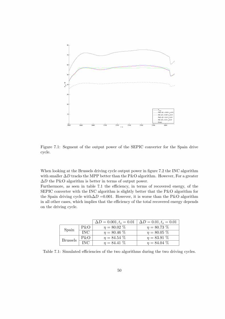
2640 2660 2680 2700 2720 2740 2760 2780 28000
10
20
30
40
50
60
70
80
t / s
Po
ut /
W
Pmax
P&O ∆D = 0.001 ts=0.01
INC ∆D = 0.001 ts=0.01
P&O ∆D = 0.01 ts=0.01
INC ∆D = 0.01 ts=0.01
Direct
Figure 7.1: Segment of the output power of the SEPIC converter for the Spain drivecycle.
When looking at the Brussels driving cycle output power in figure 7.2 the INC algorithmwith smaller ∆D tracks the MPP better than the P&O algorithm. However, For a greater∆D the P&O algorithm is better in terms of output power.Furthermore, as seen in table 7.1 the efficiency, in terms of recovered energy, of theSEPIC converter with the INC algorithm is slightly better that the P&O algorithm forthe Spain driving cycle with∆D =0.001. However, it is worse than the P&O algorithmin all other cases, which implies that the efficiency of the total recovered energy dependson the driving cycle.
∆D = 0.001, ts = 0.01 ∆D = 0.01, ts = 0.01
SpainP&O η = 80.02 % η = 80.73 %INC η = 80.46 % η = 80.05 %
BrusselsP&O η = 84.54 % η = 83.91 %INC η = 84.41 % η = 84.04 %
Table 7.1: Simulated efficiencies of the two algorithms during the two driving cycles.
50
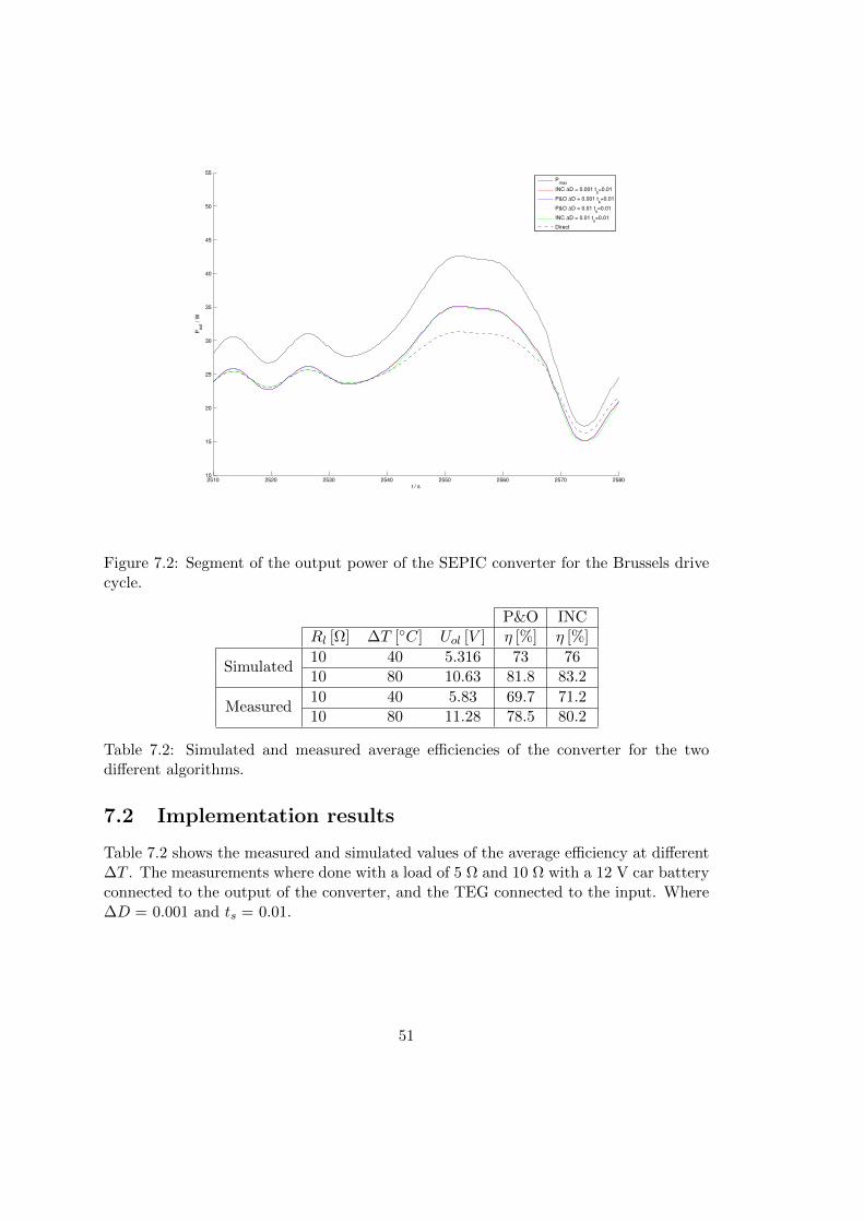
2510 2520 2530 2540 2550 2560 2570 258010
15
20
25
30
35
40
45
50
55
t / s
Po
ut /
W
Pmax
INC ∆D = 0.001 ts=0.01
P&O ∆D = 0.001 ts=0.01
P&O ∆D = 0.01 ts=0.01
INC ∆D = 0.01 ts=0.01
Direct
Figure 7.2: Segment of the output power of the SEPIC converter for the Brussels drivecycle.
P&O INCRl [Ω] ∆T [C] Uol [V ] η [%] η [%]
Simulated10 40 5.316 73 7610 80 10.63 81.8 83.2
Measured10 40 5.83 69.7 71.210 80 11.28 78.5 80.2
Table 7.2: Simulated and measured average efficiencies of the converter for the twodifferent algorithms.
7.2 Implementation results
Table 7.2 shows the measured and simulated values of the average efficiency at different∆T . The measurements where done with a load of 5 Ω and 10 Ω with a 12 V car batteryconnected to the output of the converter, and the TEG connected to the input. Where∆D = 0.001 and ts = 0.01.
51

52
Chapter 8
Conclusion
This project had three objectives, the first objective was to evaluate a suitable converterto be connected to the TEG with 12 V lead-acid battery and a resistive load. It wasfound that the SEPIC converter was the most suitable for this purpose.This was due to the fact that it is non-inverting, which is better when implementingin a electrical system. Furthermore, the switch never disconnects the TEG, which wasimportant since maximum power harvesting was the focus.However, comparing it to the Buck-Boost converter, it has twice the amount of passivecomponents. This means that the production cost of the SEPIC converter will be highercompared to the Buck-Boost converter, but at the same time it will be more efficient.
Further on, the second objective was to evaluate a suitable MPPT control algorithm.Based on previous studies, the P&O and the INC algorithm was simulated and evalu-ated. The results show that a smaller ∆D and a larger ts yields better tracking abilityand stability.The results show that the INC algorithm tracks the power better than the P&O algo-rithm. Comparing the INC algorithm to the P&O algorithm, is more stable and couldwithstand disturbances. However, when simulating the algorithms in a driving cycle,the total recovered energy is in some cases higher with the P&O algorithm. This impliesthat the efficiency of the converter in terms of recovered energy depends on the drivingstyle. Since the temperature will vary with different time constants, the algorithms willsometimes not catch up to the actual MPP.
The third objective, was to implement the suitable converter, in this case the SEPIC con-verter, with both algorithms. The results show that the INC algorithm is more efficientcompared to the P&O algorithm. However, the INC algorithm is more computationalheavy compared to the P&O algorithm.
53

54

Chapter 9
Discussion
As in any project, there is room for further investigation. This project’s implementationand design was based on a previous TEG with an output power of roughly 20 W, whichis too small for implementation in a HDV.The aim is to reach an output power of roughly 5 kW in the future, to make the TEGbeneficial. However, in this power range the currents increase along with the ratings ofthe components. This means that the components will be larger in size and the losseswill increase.
Due to these effects the full bridge converter might be a better choice as a converter.Firstly since the conversion is mainly done by transistors, which means that the size ofthe converter will be small even for high current ratings. Secondly, the passive com-ponents will only be used for filtering and thus be fewer. However, this needs moreinvestigation and analysis.
Furthermore, the use of TEGs in hybrid HVD’s are of high interest. This is due tothe driving style of a HDV, which is usually long haulage. Hence, regeneration causedby braking will occur rarely. This implies that a TEG could be beneficial during longhaulage driving cycles, due to the generation of extra power. However, this also needsinvestigation and analysis.
55

56
Bibliography
[1] Henrik Schauman. The thermoelectric generator, an analysis of seebeck-based wasteheat recovery in a scania r-series truck, master thesis. Royal Institute of Technology,2009.
[2] D. M. Rowe. Thermoelectrics and its energy harvesting, Modules, systems, andapplications in thermoelectrics. 2012.
[3] D. M. Rowe. Thermoelectrics handbook, Macro to Nano. 2006.
[4] J. C. Bass, N. B. Elsner, and F. A. Leavitt. Performance of the 1kw thermoelectricgenerator for diesel engines. 1994.
[5] J. LaGrandeur, D. Crane, S. Hung, B. Mazar, and A. Eder. Automotive waste heatconversion to electric power using skutterudite, tags, pbte and bite. 2006.
[6] Adham Shawwaf. Optimization of the electric properties of thermoelectric genera-tors, master thesis. Lund University, 2010.
[7] A. Thenkani and N. Dr. Senthil Kumar. Design of optimum maximum power pointtracking algorithm for solar panel. 2011.
[8] D. M. Rowe. CRC Handbook of Thermoelectrics. 1995.
[9] Ned Mohan, Tore M. Undeland, and William P. Robbins. Power electronics, Con-verters, Applications and Design. Second edition edition, 1995.
[10] Ph.D. Muhammad H. Rashid. Power electronics handbook, Devices, Circuits andApplications. Third edition edition, 2011.
[11] Ben Schaeffer and Dennis Gilbert. Analysis of the sepic converter. 2010.
[12] I. Laird, H. Lovatt, N. Savvides, D. Lu, and V. G. Agelidis. Comparative sudy ofmaximum power point tracking algorithms for thermoelectric generators. 2008.
57

58

Appendices
59

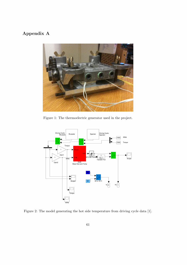
Appendix A
Figure 1: The thermoelectric generator used in the project.
RPM
Torque
Torque
RPM
Tc 2 Th 1
Transfer Fcn
1
15s+1
Torque
Scope1
Scope
RPM
1500
1400
30
80
MATLAB Function
u t
fcn
Gain2
1
Gain1
1
EGRMass flow and Temp
Torque
RPM
Out2
Driving Cycle: Spanien
SpanienDriving Cycle:
Brussels Brussels
80 or 30 C
Figure 2: The model generating the hot side temperature from driving cycle data [1].
61
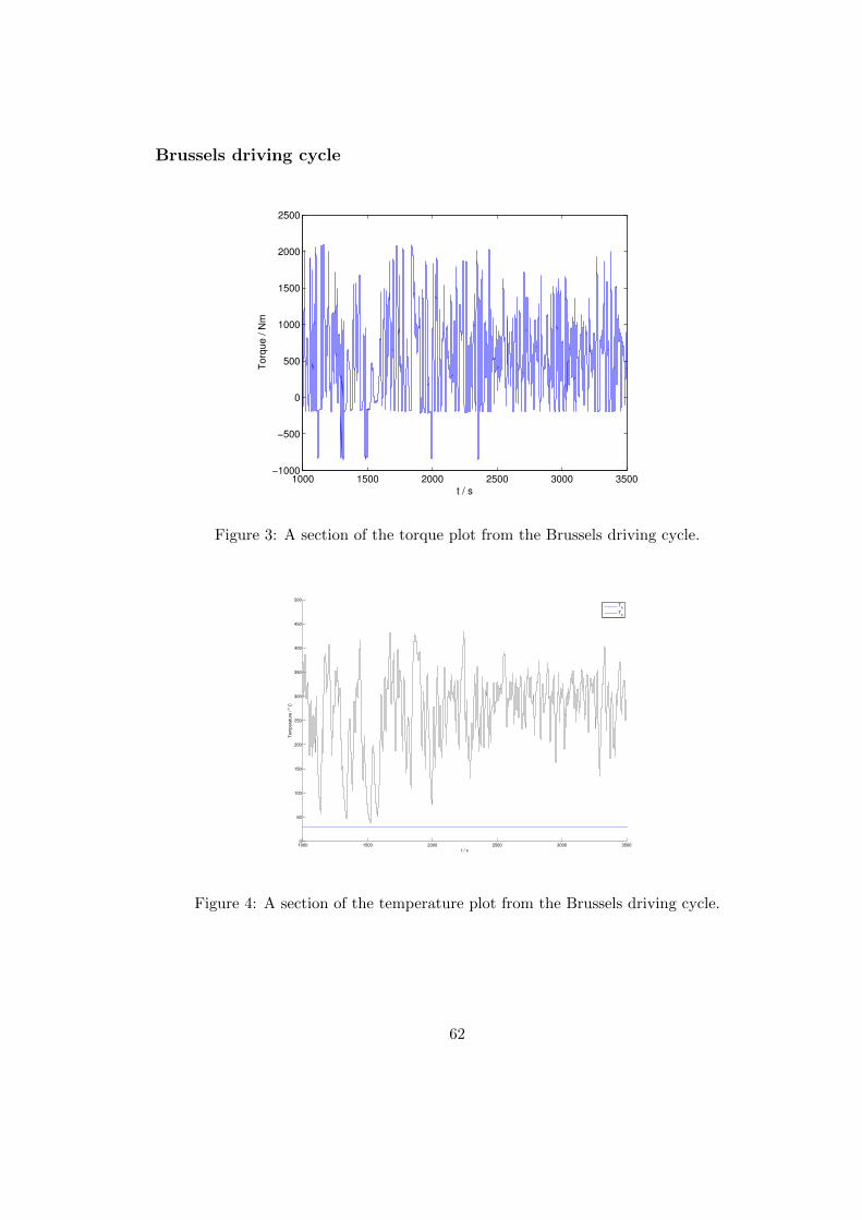
Brussels driving cycle
1000 1500 2000 2500 3000 3500−1000
−500
0
500
1000
1500
2000
2500
t / s
Torq
ue / N
m
Figure 3: A section of the torque plot from the Brussels driving cycle.
1000 1500 2000 2500 3000 35000
50
100
150
200
250
300
350
400
450
500
t / s
Tem
pera
ture
/ ο
C
Th
Th
Figure 4: A section of the temperature plot from the Brussels driving cycle.
62
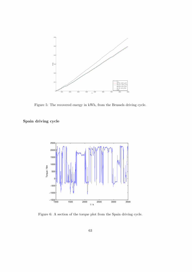
1000 2000 3000 4000 5000 6000 7000 8000 90000
0.01
0.02
0.03
0.04
0.05
0.06
t / s
Energ
y
Pmax
INC ∆D = 0.001 ts=0.01
P&O ∆D = 0.001 ts=0.01
P&O ∆D = 0.01 ts=0.01
INC ∆D = 0.01 ts=0.01
Direct
Figure 5: The recovered energy in kWh, from the Brussels driving cycle.
Spain driving cycle
1000 1500 2000 2500 3000 3500−1500
−1000
−500
0
500
1000
1500
2000
2500
t / s
Torq
ue / N
m
Figure 6: A section of the torque plot from the Spain driving cycle.
63
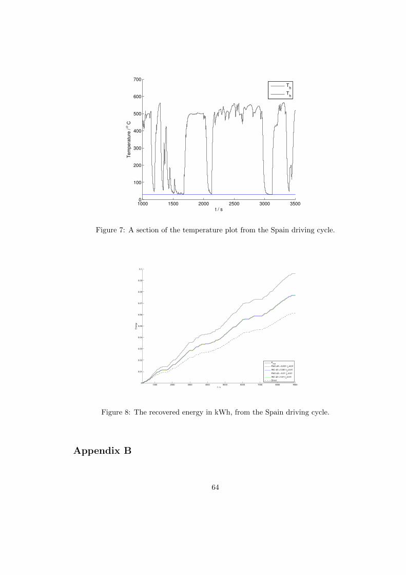
1000 1500 2000 2500 3000 35000
100
200
300
400
500
600
700
t / s
Tem
pera
ture
/ ο
C
Th
Th
Figure 7: A section of the temperature plot from the Spain driving cycle.
1000 2000 3000 4000 5000 6000 7000 8000 90000
0.01
0.02
0.03
0.04
0.05
0.06
0.07
0.08
0.09
0.1
t / s
Energ
y
Pmax
P&O ∆D = 0.001 ts=0.01
INC ∆D = 0.001 ts=0.01
P&O ∆D = 0.01 ts=0.01
INC ∆D = 0.01 ts=0.01
Direct
Figure 8: The recovered energy in kWh, from the Spain driving cycle.
Appendix B
64
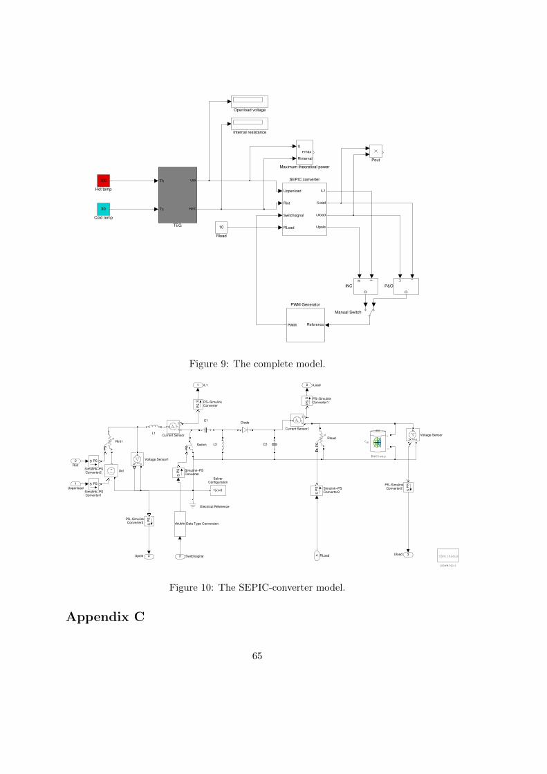
TEG
Th
Tc
Uol
Rint
SEPIC converter
Uopenload
Rint
Switchsignal
RLoad
iL1
iLoad
Uload
Upole
Rload
10
Pout
PWM Generator
ReferencePWM
P&O
u i
D
Openload voltage
Maximum theoretical power
U
Rinternal
Pmax
Manual Switch
Internal resistance
INC
U I
D
Hot temp
100
Cold temp
30
Figure 9: The complete model.
Upole 4Uload 3
iLoad2iL11
powergui
Continuous
Voltage Sensor1
V+
−
Voltage Sensor
V+
−
Uol
Switch
PS
SolverConfiguration
f(x)=0Simulink−PSConverter3
PS
S
Simulink−PSConverter2
PSS
Simulink−PSConverter1
PSS
Simulink−PSConverter
PS
S
Rload
PS
+−
Rint1
PS
+−
PS−SimulinkConverter3
PS
S
PS−SimulinkConverter2
PS
S
PS−SimulinkConverter1P
SS
PS−SimulinkConverterP
SS
L2
+−
L1
+ −
Electrical Reference
Diode
+ −
Data Type Conversiondouble
Current Sensor1
I+
−
Current Sensor
I+
−
C2
+−
C1
+−
Battery
+
_
m
RLoad4Switchsignal3
Rint
2
Uopenload
1
Figure 10: The SEPIC-converter model.
Appendix C
65
D
1
TransportDelay1
TransportDelay
Switch
>
Saturation
RelationalOperator1
>
RelationalOperator
>
Product2
Product1
MemoryLogical
Operator
NXOR
Constant3
dD
Constant2
1
Constant1
−1Add2
i2u1
Figure 11: The perturb and observe algorithm model.
D1
TransportDelay1
TransportDelay
Switch
>
SaturationRelationalOperator
<
Product2
Product1
Memory
Divide2
Divide1
Constant3
dD
Constant2
1
Constant1
−1
Constant
−1
Add2
Add1
Add
I2
U
1
Figure 12: The incremental conductance algorithm model.
First run the init . files
Temp
Th
Tc
TEG
T hot
T cold
Pmax
Plot
Power
Energy
Temperature
Integrator
Power Energy
Converter
Pmax
Th
Tc
Pconv
Figure 13: The mapping model.
66
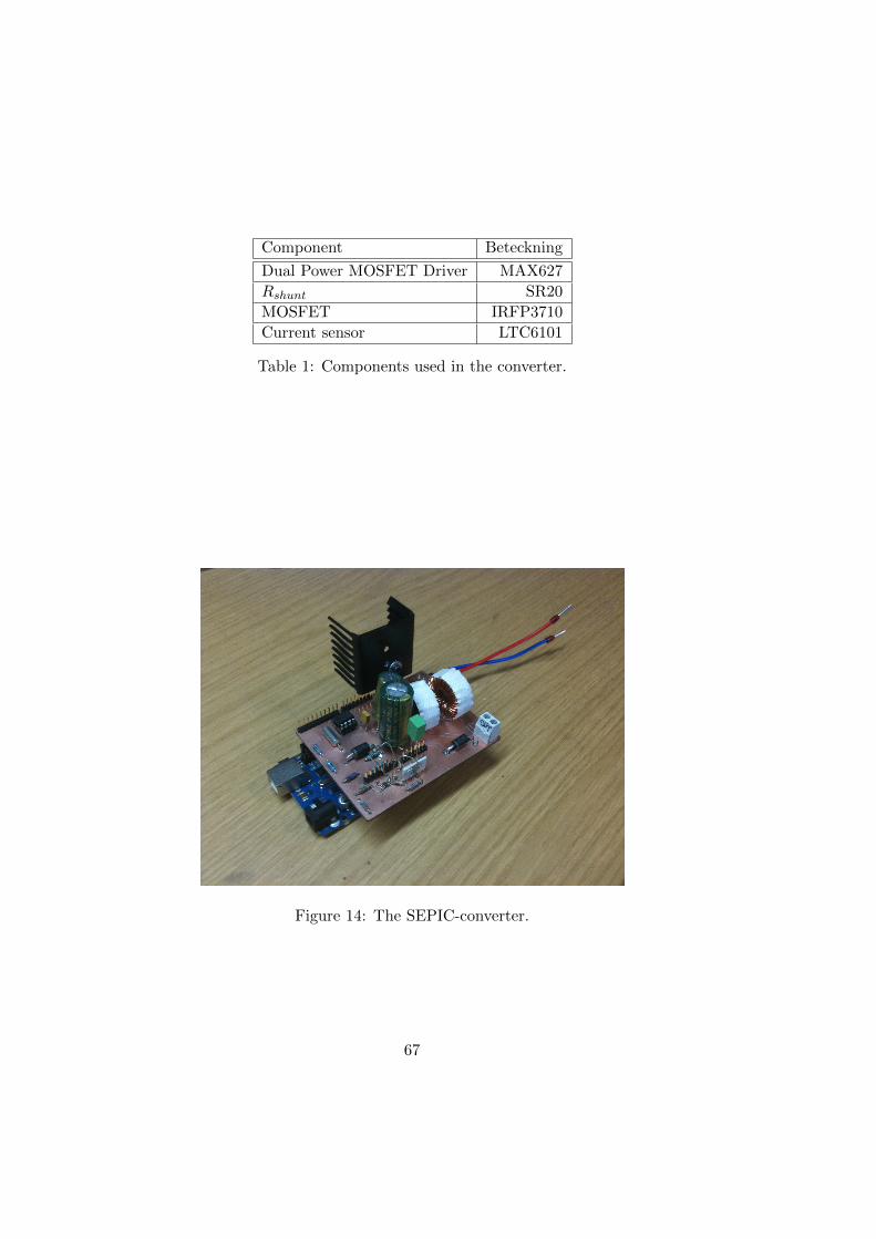
Component Beteckning
Dual Power MOSFET Driver MAX627
Rshunt SR20
MOSFET IRFP3710
Current sensor LTC6101
Table 1: Components used in the converter.
Figure 14: The SEPIC-converter.
67
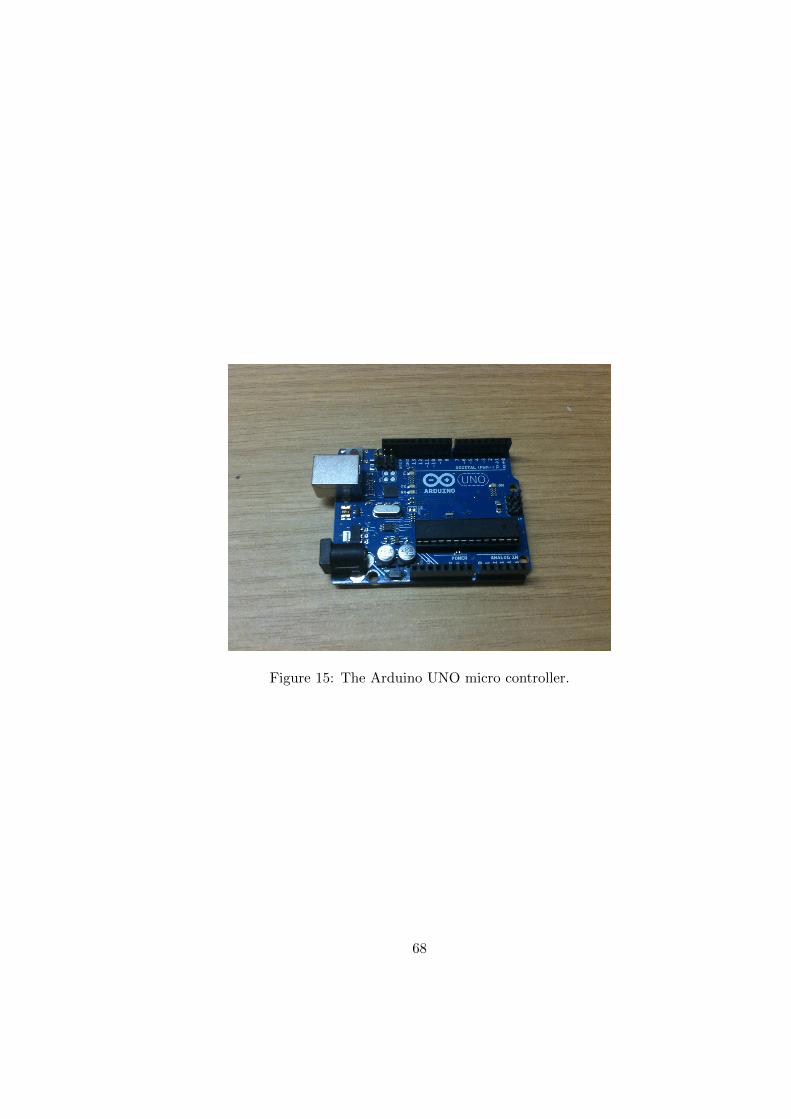
Figure 15: The Arduino UNO micro controller.
68


![2092 IEEE TRANSACTIONS ON INDUSTRIAL ELECTRONICS, VOL. … · is a dc/ac converter [1]–[4]. In this case, the dc/dc converter performs the maximum power point tracking (MPPT) control,](https://img.pdfslide.net/doc/110x75/5f4693d58b37db50d3650a32/2092-ieee-transactions-on-industrial-electronics-vol-is-a-dcac-converter-1a4.jpg)