Embed Size (px)
Citation preview
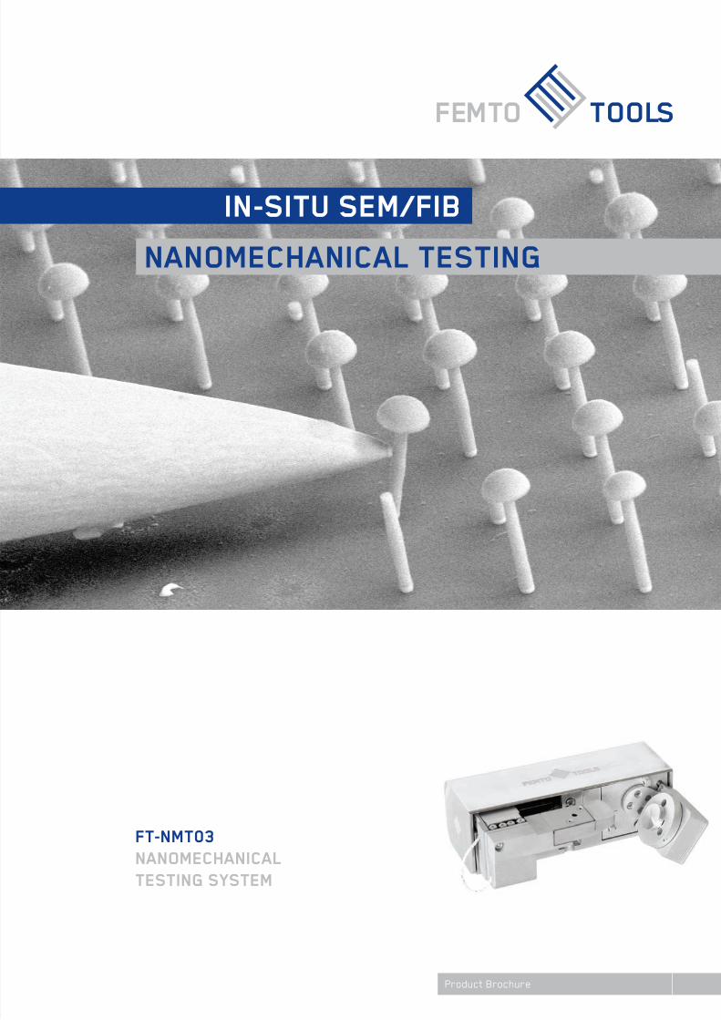
FEMTO TOOLS
in-siTu sem/FiB
nanomechanical TesTing
FT-nmT03nanomechanical TesTing sysTem
Product Brochure
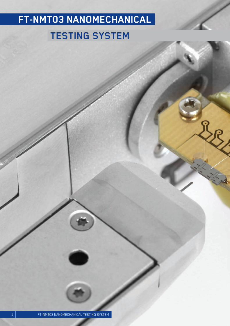
TesTing sysTem
FT-nmT03 nanomechanical
1 FT-NMT03 NANOMECHANICAL TESTING SYSTEM
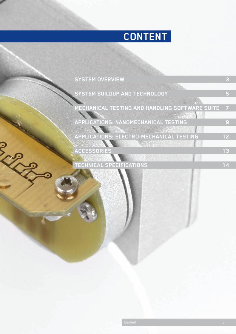
conTenT
sysTem overview 3
applicaTions: elecTro-mechanical TesTing 12
sysTem Buildup and Technology 5
accessories 13
applicaTions: nanomechanical TesTing 9
Technical speciFicaTions 14
mechanical TesTing and handling soFTware suiTe 7
2Content
TesTing sysTem
FT-nmT03 nanomechanical
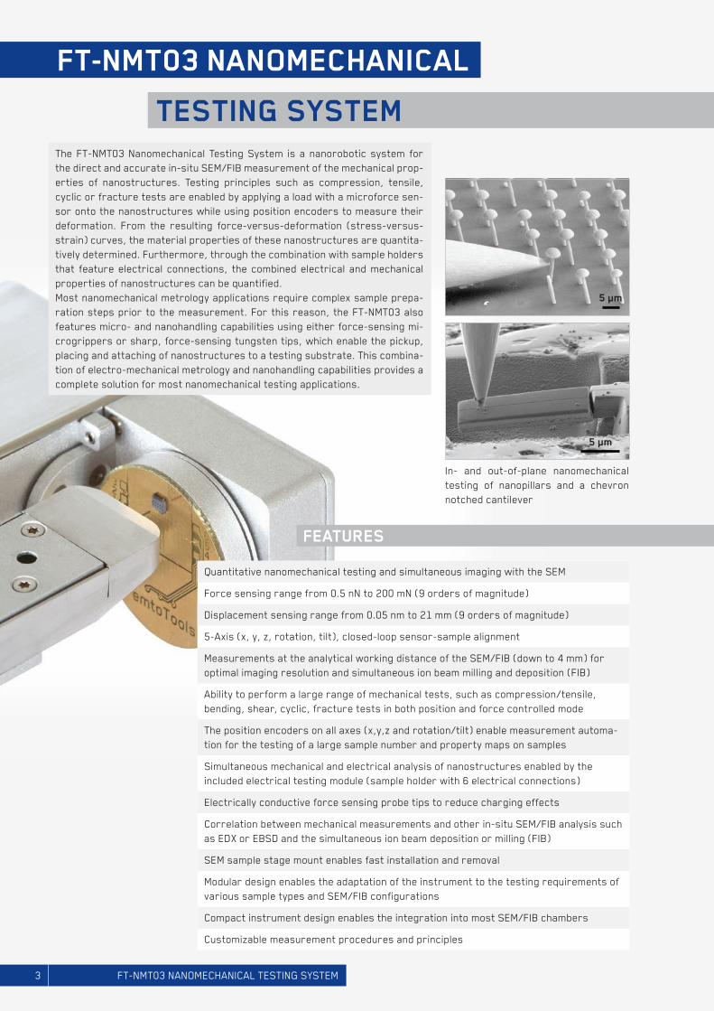
The FT-NMT03 Nanomechanical Testing System is a nanorobotic system for the direct and accurate in-situ SEM/FIB measurement of the mechanical prop-erties of nanostructures. Testing principles such as compression, tensile, cyclic or fracture tests are enabled by applying a load with a microforce sen-sor onto the nanostructures while using position encoders to measure their deformation. From the resulting force-versus-deformation (stress-versus-strain) curves, the material properties of these nanostructures are quantita-tively determined. Furthermore, through the combination with sample holders that feature electrical connections, the combined electrical and mechanical properties of nanostructures can be quantified. Most nanomechanical metrology applications require complex sample prepa-ration steps prior to the measurement. For this reason, the FT-NMT03 also features micro- and nanohandling capabilities using either force-sensing mi-crogrippers or sharp, force-sensing tungsten tips, which enable the pickup, placing and attaching of nanostructures to a testing substrate. This combina-tion of electro-mechanical metrology and nanohandling capabilities provides a complete solution for most nanomechanical testing applications.
FeaTures
In- and out-of-plane nanomechanical testing of nanopillars and a chevron notched cantilever
Displacement sensing range from 0.05 nm to 21 mm (9 orders of magnitude)
Quantitative nanomechanical testing and simultaneous imaging with the SEM
Measurements at the analytical working distance of the SEM/FIB (down to 4 mm) for optimal imaging resolution and simultaneous ion beam milling and deposition (FIB)
The position encoders on all axes (x,y,z and rotation/tilt) enable measurement automa-tion for the testing of a large sample number and property maps on samples
Electrically conductive force sensing probe tips to reduce charging effects
Ability to perform a large range of mechanical tests, such as compression/tensile, bending, shear, cyclic, fracture tests in both position and force controlled mode
Simultaneous mechanical and electrical analysis of nanostructures enabled by the included electrical testing module (sample holder with 6 electrical connections)
Correlation between mechanical measurements and other in-situ SEM/FIB analysis such as EDX or EBSD and the simultaneous ion beam deposition or milling (FIB)
5-Axis (x, y, z, rotation, tilt), closed-loop sensor-sample alignment
Force sensing range from 0.5 nN to 200 mN (9 orders of magnitude)
SEM sample stage mount enables fast installation and removal
Modular design enables the adaptation of the instrument to the testing requirements of various sample types and SEM/FIB configurations
Compact instrument design enables the integration into most SEM/FIB chambers
Customizable measurement procedures and principles
3 FT-NMT03 NANOMECHANICAL TESTING SYSTEM
5 µm
5 µm
4
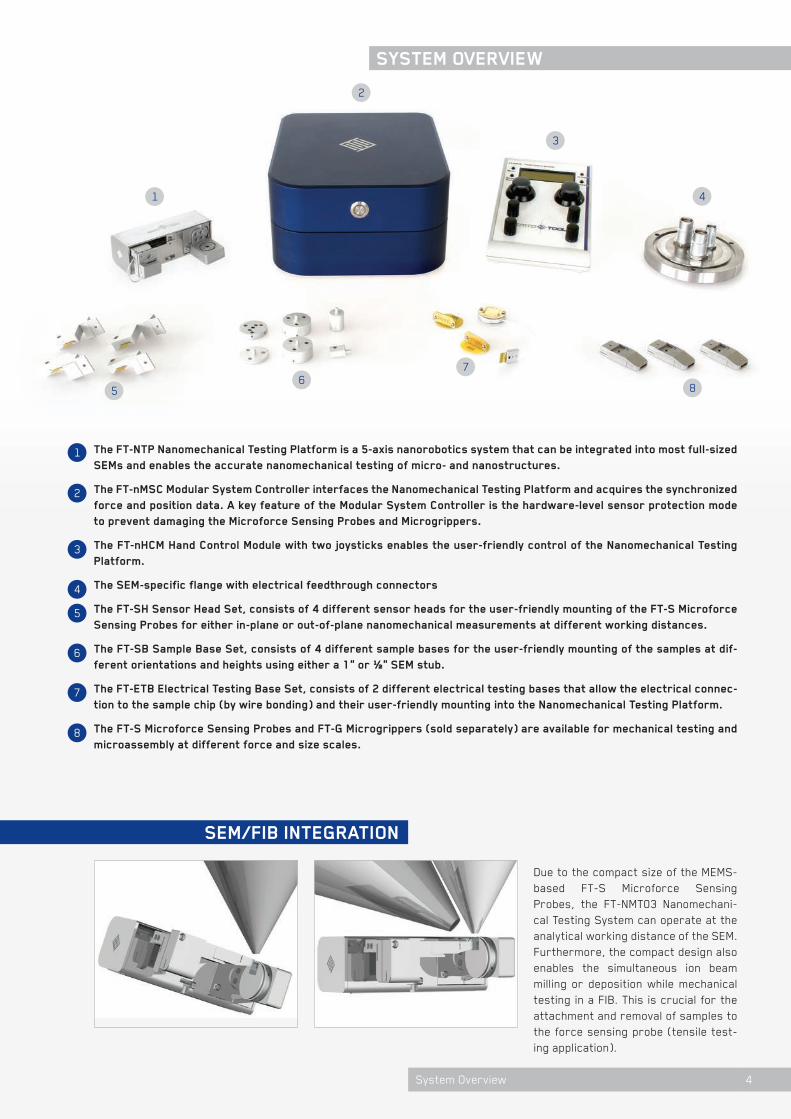
1
2
5
3
6
The FT-nTp nanomechanical Testing platform is a 5-axis nanorobotics system that can be integrated into most full-sized sems and enables the accurate nanomechanical testing of micro- and nanostructures.
The FT-nmsc modular system controller interfaces the nanomechanical Testing platform and acquires the synchronized force and position data. a key feature of the modular system controller is the hardware-level sensor protection mode to prevent damaging the microforce sensing probes and microgrippers.
The FT-nhcm hand control module with two joysticks enables the user-friendly control of the nanomechanical Testing platform.
The sem-specific flange with electrical feedthrough connectors
The FT-sh sensor head set, consists of 4 different sensor heads for the user-friendly mounting of the FT-s microforce sensing probes for either in-plane or out-of-plane nanomechanical measurements at different working distances.
The FT-sB sample Base set, consists of 4 different sample bases for the user-friendly mounting of the samples at dif-ferent orientations and heights using either a 1” or ½” sem stub.
The FT-eTB electrical Testing Base set, consists of 2 different electrical testing bases that allow the electrical connec-tion to the sample chip (by wire bonding) and their user-friendly mounting into the nanomechanical Testing platform.
The FT-s microforce sensing probes and FT-g microgrippers (sold separately) are available for mechanical testing and microassembly at different force and size scales.
sem/FiB inTegraTion
68
3
2
7
1
sysTem overview
Due to the compact size of the MEMS-based FT-S Microforce Sensing Probes, the FT-NMT03 Nanomechani-cal Testing System can operate at the analytical working distance of the SEM. Furthermore, the compact design also enables the simultaneous ion beam milling or deposition while mechanical testing in a FIB. This is crucial for the attachment and removal of samples to the force sensing probe (tensile test-ing application).
5
4
7
8
4System Overview
Technology
sysTem Buildup and
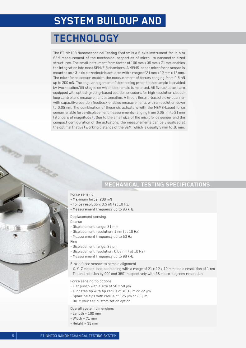
The FT-NMT03 Nanomechanical Testing System is a 5-axis instrument for in-situ SEM measurement of the mechanical properties of micro- to nanometer sized structures. The small instrument form factor of 100 mm x 35 mm x 71 mm enables the integration into most SEM/FIB chambers. A MEMS-based microforce sensor is mounted on a 3-axis piezoelectric actuator with a range of 21 mm x 12 mm x 12 mm. The microforce sensor enables the measurement of forces ranging from 0.5 nN up to 200 mN. The angular alignment of the sensing probe to the sample is enabled by two rotation/tilt stages on which the sample is mounted. All five actuators are equipped with optical-grating-based position encoders for high resolution closed-loop control and measurement automation. A linear, flexure-based piezo-scanner with capacitive position feedback enables measurements with a resolution down to 0.05 nm. The combination of these six actuators with the MEMS-based force sensor enable force-displacement measurements ranging from 0.05 nm to 21 mm (9 orders of magnitude) . Due to the small size of the microforce sensor and the compact configuration of the actuators, the measurements can be visualized at the optimal (native) working distance of the SEM, which is usually 5 mm to 10 mm.
mechanical TesTing speciFicaTions
5-axis force sensor to sample alignment - X, Y, Z closed-loop positioning with a range of 21 x 12 x 12 mm and a resolution of 1 nm- Tilt and rotation by 90° and 360° respectively with 35 micro-degrees resolution
Force sensing - Maximum force: 200 mN - Force resolution: 0.5 nN (at 10 Hz) - Measurement frequency up to 96 kHz
Overall system dimensions - Length = 100 mm- Width = 71 mm- Height = 35 mm
Force sensing tip options- Flat punch with a size of 50 x 50 µm- Tungsten tip with tip radius of ≤0.1 µm or ≤2 µm - Spherical tips with radius of 125 µm or 25 µm- Do-it-yourself customization option
Displacement sensing Coarse- Displacement range: 21 mm - Displacement resolution: 1 nm (at 10 Hz)- Measurement frequency up to 50 HzFine- Displacement range: 25 µm - Displacement resolution: 0.05 nm (at 10 Hz)- Measurement frequency up to 96 kHz
5 FT-NMT03 NANOMECHANICAL TESTING SYSTEM
4
1
2
5
6
3
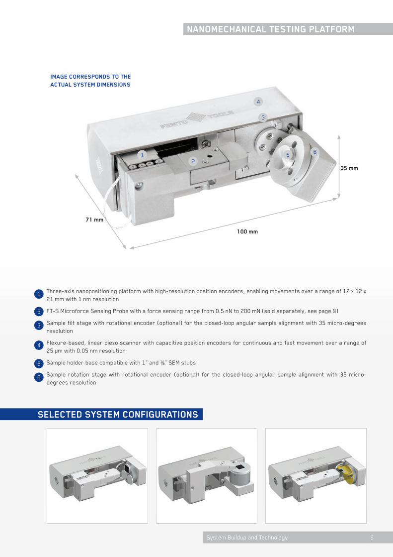
Three-axis nanopositioning platform with high-resolution position encoders, enabling movements over a range of 12 x 12 x 21 mm with 1 nm resolution
FT-S Microforce Sensing Probe with a force sensing range from 0.5 nN to 200 mN (sold separately, see page 9)
Sample tilt stage with rotational encoder (optional) for the closed-loop angular sample alignment with 35 micro-degrees resolution
Flexure-based, linear piezo scanner with capacitive position encoders for continuous and fast movement over a range of 25 µm with 0.05 nm resolution
Sample holder base compatible with 1” and ½” SEM stubs
Sample rotation stage with rotational encoder (optional) for the closed-loop angular sample alignment with 35 micro-degrees resolution
selecTed sysTem conFiguraTions
1
4
3
6
25
nanomechanical TesTing plaTForm
image corresponds To The acTual sysTem dimensions
100 mm
71 mm
35 mm
6System Buildup and Technology
and handling soFTware suiTe
mechanical TesTing
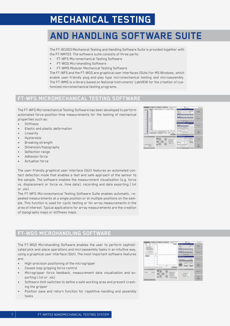
The FT-WFS Micromechanical Testing Software has been developed to perform automated force-position-time measurements for the testing of mechanical properties such as:• Stiffness• Elastic and plastic deformation• Linearity• Hysteresis• Breaking strength• Dimension/topography• Deflection range• Adhesion force• Actuation force
The user-friendly graphical user interface (GUI) features an automated con-tact detection mode that enables a fast and safe approach of the sensor to the sample. The software enables the measurement visualization (e.g. force vs. displacement or force vs. time data), recording and data exporting (.txt or .xls).The FT-WFS Micromechanical Testing Software Suite enables automatic, re-peated measurements at a single position or at multiple positions on the sam-ple. This function is used for cyclic testing or for array measurements in the area of interest. Typical applications for array measurements are the creation of topography maps or stiffness maps.
The FT-WGS Microhandling Software enables the user to perform sophisti-cated pick-and-place operations and microassembly tasks in an intuitive way, using a graphical user interface (GUI). The most important software features are:• High-precision positioning of the microgripper• Closed-loop gripping force control• Microgripper force feedback, measurement data visualization and ex-
porting (.txt or .xls)• Software limit switches to define a safe working area and prevent crash-
ing the gripper• Position save and return function for repetitive handling and assembly
tasks
FT-wFs micromechanical TesTing soFTware
FT-wgs microhandling soFTware
The FT-W1003 Mechanical Testing and Handling Software Suite is provided together with the FT-NMT03. The software suite consists of three parts:• FT-WFS Micromechanical Testing Software• FT-WGS Microhandling Software• FT-WMS Modular Mechanical Testing SoftwareThe FT-WFS and the FT-WGS are graphical user interfaces (GUIs) for MS Windows, which enable user-friendly plug-and-play type micromechanical testing and microassembly. The FT-WMS is a library based on National Instruments’ LabVIEW for the creation of cus-tomized micromechanical testing programs.
7 FT-NMT03 NANOMECHANICAL TESTING SYSTEM
4
1
2
3
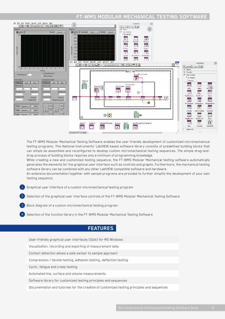
The FT-WMS Modular Mechanical Testing Software enables the user-friendly development of customized micromechanical testing programs. This National Instruments’ LabVIEW based software library consists of predefined building blocks that can simply be assembled and reconfigured to develop custom micromechanical testing sequences. The simple drag-and-drop process of building blocks requires only a minimum of programming knowledge. While creating a new and customized testing sequence, the FT-WMS Modular Mechanical testing software automatically generates the elements for the graphical user interface such as controls and graphs. Furthermore, the mechanical testing software library can be combined with any other LabVIEW compatible software and hardware. An extensive documentation together with sample programs are provided to further simplify the development of your own testing sequence.
Graphical user interface of a custom micromechanical testing program
Selection of the graphical user interface controls of the FT-WMS Modular Mechanical Testing Software
Block diagram of a custom micromechanical testing program
Selection of the function library in the FT-WMS Modular Mechanical Testing Software
FeaTures
1
43
2
Contact detection allows a safe sensor to sample approach
User-friendly graphical user interfaces (GUIs) for MS Windows
Cyclic, fatigue and creep testing
Software library for customized testing principles and sequences
Automated line, surface and volume measurements
Documentation and tutorials for the creation of customized testing principles and sequences
Compression / tensile testing, adhesion testing, deflection testing
Visualization, recording and exporting of measurement data
FT-wms modular mechanical TesTing soFTware
8Micromechanical Testing and Handling Software Suite
applicaTion examples
0 5 10 15 20
App
lied
forc
e (m
N)
Deformation (µm)
0
3
2
1
4
0 2.5 10 15 2 0
App
lied
forc
e (m
N)
Deformation (µm)
0
20
10
30
0 2.5 5 7.5 10
App
lied
forc
e (m
N)
Deformation (µm)
0
20
10
30
without thermal treatmentwith thermal treatment
Engineering strain
Engi
neer
ing
stre
ss (
MPa
)
0
a
0.1 0.15 0.20
200
400
600
800
1000
Engi
neer
ing
stra
in
0
0.05
0.10
0.15
0.20
0.25
0 500 1000 1500 2000 2500
10.010.5
9.5Forc
e
0.6 mW
0.9 mW
1.0 mW
1.1 mW
1.2 mW
Elastic limit
Applied force (µN) 0 20 40 60 80 100
Out
put
volt
age
chan
ge (
mV)
0
10
20
30
40
50
60
cantilever 1cantilever 2
0 2.5 5 7.5 10 12.5 15 17.5 20−20
0
20
40
60
80
100
App
lied
forc
e (µ
N)
Sample deflection (µm)
0 1 2 3 4 5 6 7 8−1
0
1
2
App
lied
forc
e (µ
N)
Sample deflection (µm)
Time (s)
Act
uati
on f
orce
(µN
)
0 0.5 1 1.5 2 2.5-20
0
20
40
60
80
Sam
ple
defle
ctio
n (µ
m)
0
5
15
10
20
1.5
0.5
-0.5
Time (s)
(µN
)
0.05
bc d/e
ca b
Because of the high surface-to-volume ratio, nanostructures are ideal for the creation of high sensitivity sensors, such as gas detectors. Using a combi-nation of nanolithography and electro-plating, 3D metallic nanostructures, can be fabricated. Both, the resulting material properties and geometry have high variations. Quantitative insights into the behavior of these nanopillars is obtained by nanomechanical testing. Image courtesy: Prof. Bradley Nelson, ETH Zurich, Switzerland
in-plane nanomechanical TesTing oF 3d meTallic nanopillars
nanomechanical TesTing
Microscaffolds are used in various ar-eas such as in material science for the creation of ultra-light materials or in biology as a cellular environment with a predefined mechanical rigidity, used for the growth of artificial tissues. Compression testing of scaffolds ena-bles the determination of their elastic and plastic behavior even beyond the collapsing point. Image courtesy: ETH Zurich, Switzerland
sTaBle compression TesTing oF microscaFFolds
0 5 10 15 20
App
lied
forc
e (m
N)
Deformation (µm)
0
3
2
1
4
0 2.5 10 15 2 0
App
lied
forc
e (m
N)
Deformation (µm)
0
20
10
30
0 2.5 5 7.5 10
App
lied
forc
e (m
N)
Deformation (µm)
0
20
10
30
without thermal treatmentwith thermal treatment
Engineering strain
Engi
neer
ing
stre
ss (
MPa
)
0
a
0.1 0.15 0.20
200
400
600
800
1000
Engi
neer
ing
stra
in
0
0.05
0.10
0.15
0.20
0.25
0 500 1000 1500 2000 2500
10.010.5
9.5Forc
e
0.6 mW
0.9 mW
1.0 mW
1.1 mW
1.2 mW
Elastic limit
Applied force (µN) 0 20 40 60 80 100
Out
put
volt
age
chan
ge (
mV)
0
10
20
30
40
50
60
cantilever 1cantilever 2
0 2.5 5 7.5 10 12.5 15 17.5 20−20
0
20
40
60
80
100
App
lied
forc
e (µ
N)
Sample deflection (µm)
0 1 2 3 4 5 6 7 8−1
0
1
2A
pplie
d fo
rce
(µN
)
Sample deflection (µm)
Time (s)
Act
uati
on f
orce
(µN
)
0 0.5 1 1.5 2 2.5-20
0
20
40
60
80
Sam
ple
defle
ctio
n (µ
m)
0
5
15
10
20
1.5
0.5
-0.5
Time (s)
(µN
)
0.05
bc d/e
ca b
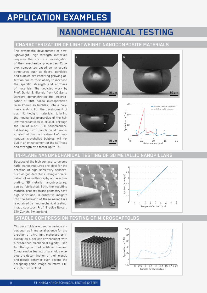
The systematic development of new, lightweight, high-strength materials requires the accurate investigation of their mechanical properties. Com-plex composites based on nanoscale structures such as fibers, particles and bubbles are receiving growing at-tention due to their ability to increase the specific strength and stiffness of materials. The depicted work by Prof. Daniel S. Gianola from UC Santa Barbara demonstrates the incorpo-ration of stiff, hollow microparticles (also known as bubbles) into a poly-meric matrix. For the development of such lightweight materials, tailoring the mechanical properties of the hol-low microparticles is crucial. Through the use of in-situ SEM nanomechani-cal testing, Prof Gianola could demon-strate that thermal treatment of these nanoparticle-shelled bubbles will re-sult in an enhancement of the stiffness and strength by a factor up to 14.
characTerizaTion oF lighTweighT nanocomposiTe maTerials
10 µm
0 5 10 15 20
App
lied
forc
e (m
N)
Deformation (µm)
0
3
2
1
4
0 2.5 10 15 2 0
App
lied
forc
e (m
N)
Deformation (µm)
0
20
10
30
0 2.5 5 7.5 10
App
lied
forc
e (m
N)
Deformation (µm)
0
20
10
30
without thermal treatmentwith thermal treatment
Engineering strain
Engi
neer
ing
stre
ss (
MPa
)
0
a
0.1 0.15 0.20
200
400
600
800
1000
Engi
neer
ing
stra
in
0
0.05
0.10
0.15
0.20
0.25
0 500 1000 1500 2000 2500
10.010.5
9.5Forc
e
0.6 mW
0.9 mW
1.0 mW
1.1 mW
1.2 mW
Elastic limit
Applied force (µN) 0 20 40 60 80 100
Out
put
volt
age
chan
ge (
mV)
0
10
20
30
40
50
60
cantilever 1cantilever 2
0 2.5 5 7.5 10 12.5 15 17.5 20−20
0
20
40
60
80
100
App
lied
forc
e (µ
N)
Sample deflection (µm)
0 1 2 3 4 5 6 7 8−1
0
1
2
App
lied
forc
e (µ
N)
Sample deflection (µm)
Time (s)
Act
uati
on f
orce
(µN
)
0 0.5 1 1.5 2 2.5-20
0
20
40
60
80
Sam
ple
defle
ctio
n (µ
m)
0
5
15
10
20
1.5
0.5
-0.5
Time (s)
(µN
)
0.05
bc d/e
ca b
10 µm
10 µm
9 FT-NMT03 NANOMECHANICAL TESTING SYSTEM
5 µm
5 µm
a b
c
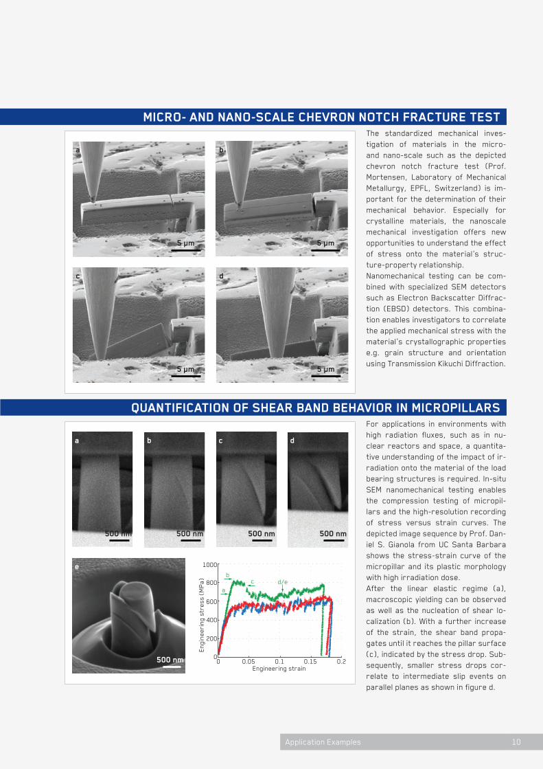
micro- and nano-scale chevron noTch FracTure TesT
QuanTiFicaTion oF shear Band Behavior in micropillars
The standardized mechanical inves-tigation of materials in the micro- and nano-scale such as the depicted chevron notch fracture test (Prof. Mortensen, Laboratory of Mechanical Metallurgy, EPFL, Switzerland) is im-portant for the determination of their mechanical behavior. Especially for crystalline materials, the nanoscale mechanical investigation offers new opportunities to understand the effect of stress onto the material’s struc-ture-property relationship. Nanomechanical testing can be com-bined with specialized SEM detectors such as Electron Backscatter Diffrac-tion (EBSD) detectors. This combina-tion enables investigators to correlate the applied mechanical stress with the material’s crystallographic properties e.g. grain structure and orientation using Transmission Kikuchi Diffraction.
For applications in environments with high radiation fluxes, such as in nu-clear reactors and space, a quantita-tive understanding of the impact of ir-radiation onto the material of the load bearing structures is required. In-situ SEM nanomechanical testing enables the compression testing of micropil-lars and the high-resolution recording of stress versus strain curves. The depicted image sequence by Prof. Dan-iel S. Gianola from UC Santa Barbara shows the stress-strain curve of the micropillar and its plastic morphology with high irradiation dose. After the linear elastic regime (a), macroscopic yielding can be observed as well as the nucleation of shear lo-calization (b). With a further increase of the strain, the shear band propa-gates until it reaches the pillar surface (c), indicated by the stress drop. Sub-sequently, smaller stress drops cor-relate to intermediate slip events on parallel planes as shown in figure d.
0 5 10 15 20
App
lied
forc
e (m
N)
Deformation (µm)
0
3
2
1
4
0 2.5 10 15 2 0
App
lied
forc
e (m
N)
Deformation (µm)
0
20
10
30
0 2.5 5 7.5 10
App
lied
forc
e (m
N)
Deformation (µm)
0
20
10
30
without thermal treatmentwith thermal treatment
Engineering strain
Engi
neer
ing
stre
ss (
MPa
)
0
a
0.1 0.15 0.20
200
400
600
800
1000
Engi
neer
ing
stra
in
0
0.05
0.10
0.15
0.20
0.25
0 500 1000 1500 2000 2500
10.010.5
9.5Forc
e
0.6 mW
0.9 mW
1.0 mW
1.1 mW
1.2 mW
Elastic limit
Applied force (µN) 0 20 40 60 80 100
Out
put
volt
age
chan
ge (
mV)
0
10
20
30
40
50
60
cantilever 1cantilever 2
0 2.5 5 7.5 10 12.5 15 17.5 20−20
0
20
40
60
80
100
App
lied
forc
e (µ
N)
Sample deflection (µm)
0 1 2 3 4 5 6 7 8−1
0
1
2
App
lied
forc
e (µ
N)
Sample deflection (µm)
Time (s)
Act
uati
on f
orce
(µN
)
0 0.5 1 1.5 2 2.5-20
0
20
40
60
80
Sam
ple
defle
ctio
n (µ
m)
0
5
15
10
20
1.5
0.5
-0.5
Time (s)
(µN
)
0.05
bc d/e
ca b
50 µm
10Application Examples
5 µm5 µm
5 µm5 µm
500 nm 500 nm 500 nm 500 nm
500 nm
a b c d
e
a b
c d
applicaTion examples
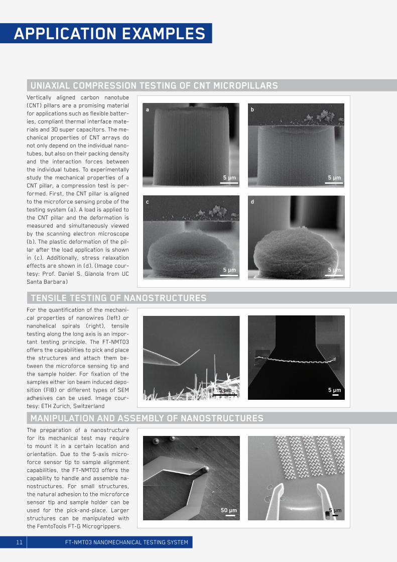
Vertically aligned carbon nanotube (CNT) pillars are a promising material for applications such as flexible batter-ies, compliant thermal interface mate-rials and 3D super capacitors. The me-chanical properties of CNT arrays do not only depend on the individual nano-tubes, but also on their packing density and the interaction forces between the individual tubes. To experimentally study the mechanical properties of a CNT pillar, a compression test is per-formed. First, the CNT pillar is aligned to the microforce sensing probe of the testing system (a). A load is applied to the CNT pillar and the deformation is measured and simultaneously viewed by the scanning electron microscope (b). The plastic deformation of the pil-lar after the load application is shown in (c). Additionally, stress relaxation effects are shown in (d). (Image cour-tesy: Prof. Daniel S. Gianola from UC Santa Barbara)
The preparation of a nanostructure for its mechanical test may require to mount it in a certain location and orientation. Due to the 5-axis micro-force sensor tip to sample alignment capabilities, the FT-NMT03 offers the capability to handle and assemble na-nostructures. For small structures, the natural adhesion to the microforce sensor tip and sample holder can be used for the pick-and-place. Larger structures can be manipulated with the FemtoTools FT-G Microgrippers.
uniaxial compression TesTing oF cnT micropillars
manipulaTion and assemBly oF nanosTrucTures
For the quantification of the mechani-cal properties of nanowires (left) or nanohelical spirals (right), tensile testing along the long axis is an impor-tant testing principle. The FT-NMT03 offers the capabilities to pick and place the structures and attach them be-tween the microforce sensing tip and the sample holder. For fixation of the samples either ion beam induced depo-sition (FIB) or different types of SEM adhesives can be used. Image cour-tesy: ETH Zurich, Switzerland
Tensile TesTing oF nanosTrucTures
5 µm50 µm
5 µm 5 µm
5 µm 5 µm
11 FT-NMT03 NANOMECHANICAL TESTING SYSTEM
5 µm5 µm
a b
c d
Thermomechanical creep TesTing oF individual meTallic glass nanowires
piezoresisTive microcanTilever array TesTing
in- and ouT-oF-plane mechanical TesTing oF mems / nems
elecTro-mechanical TesTing
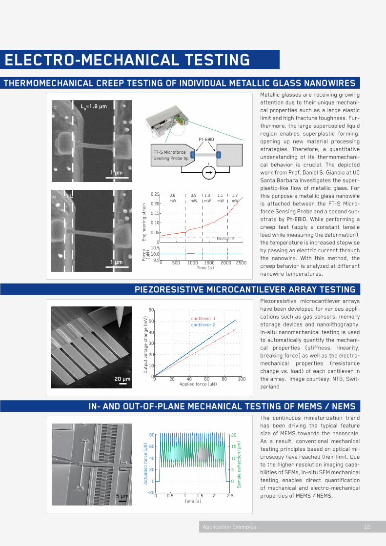
Metallic glasses are receiving growing attention due to their unique mechani-cal properties such as a large elastic limit and high fracture toughness. Fur-thermore, the large supercooled liquid region enables superplastic forming, opening up new material processing strategies. Therefore, a quantitative understanding of its thermomechani-cal behavior is crucial. The depicted work from Prof. Daniel S. Gianola at UC Santa Barbara investigates the super-plastic-like flow of metallic glass. For this purpose a metallic glass nanowire is attached between the FT-S Micro-force Sensing Probe and a second sub-strate by Pt-EBID. While performing a creep test (apply a constant tensile load while measuring the deformation), the temperature is increased stepwise by passing an electric current through the nanowire. With this method, the creep behavior is analyzed at different nanowire temperatures.
Piezoresistive microcantilever arrays have been developed for various appli-cations such as gas sensors, memory storage devices and nanolithography. In-situ nanomechanical testing is used to automatically quantify the mechani-cal properties (stiffness, linearity, breaking force) as well as the electro-mechanical properties (resistance change vs. load) of each cantilever in the array. Image courtesy: NTB, Swit-zerland
Pt-EBID
FT-S Microforce Sesning Probe tip
I
0 5 10 15 20
App
lied
forc
e (m
N)
Deformation (µm)
0
3
2
1
4
0 2.5 10 15 2 0
App
lied
forc
e (m
N)
Deformation (µm)
0
20
10
30
0 2.5 5 7.5 10
App
lied
forc
e (m
N)
Deformation (µm)
0
20
10
30
without thermal treatmentwith thermal treatment
Engineering strain
Engi
neer
ing
stre
ss (
MPa
)
0
a
0.1 0.15 0.20
200
400
600
800
1000
Engi
neer
ing
stra
in
0
0.05
0.10
0.15
0.20
0.25
0 500 1000 1500 2000 2500
10.010.5
9.5Forc
e
0.6 mW
0.9 mW
1.0 mW
1.1 mW
1.2 mW
Elastic limit
Applied force (µN) 0 20 40 60 80 100
Out
put
volt
age
chan
ge (
mV)
0
10
20
30
40
50
60
cantilever 1cantilever 2
0 2.5 5 7.5 10 12.5 15 17.5 20−20
0
20
40
60
80
100
App
lied
forc
e (µ
N)
Sample deflection (µm)
0 1 2 3 4 5 6 7 8−1
0
1
2
App
lied
forc
e (µ
N)
Sample deflection (µm)
Time (s)
Act
uati
on f
orce
(µN
)
0 0.5 1 1.5 2 2.5-20
0
20
40
60
80
Sam
ple
defle
ctio
n (µ
m)
0
5
15
10
20
1.5
0.5
-0.5
Time (s)
(µN
)
0.05
bc d/e
ca b
The continuous miniaturization trend has been driving the typical feature size of MEMS towards the nanoscale. As a result, conventional mechanical testing principles based on optical mi-croscopy have reached their limit. Due to the higher resolution imaging capa-bilities of SEMs, in-situ SEM mechanical testing enables direct quantification of mechanical and electro-mechanical properties of MEMS / NEMS.
0 5 10 15 20
App
lied
forc
e (m
N)
Deformation (µm)
0
3
2
1
4
0 2.5 10 15 2 0
App
lied
forc
e (m
N)
Deformation (µm)
0
20
10
30
0 2.5 5 7.5 10
App
lied
forc
e (m
N)
Deformation (µm)
0
20
10
30
without thermal treatmentwith thermal treatment
Engineering strain
Engi
neer
ing
stre
ss (
MPa
)
0
a
0.1 0.15 0.20
200
400
600
800
1000
Engi
neer
ing
stra
in
0
0.05
0.10
0.15
0.20
0.25
0 500 1000 1500 2000 2500
10.010.5
9.5Forc
e
0.6 mW
0.9 mW
1.0 mW
1.1 mW
1.2 mW
Elastic limit
Applied force (µN) 0 20 40 60 80 100
Out
put
volt
age
chan
ge (
mV)
0
10
20
30
40
50
60
cantilever 1cantilever 2
0 2.5 5 7.5 10 12.5 15 17.5 20−20
0
20
40
60
80
100
App
lied
forc
e (µ
N)
Sample deflection (µm)
0 1 2 3 4 5 6 7 8−1
0
1
2
App
lied
forc
e (µ
N)
Sample deflection (µm)
Time (s)
Act
uati
on f
orce
(µN
)
0 0.5 1 1.5 2 2.5-20
0
20
40
60
80
Sam
ple
defle
ctio
n (µ
m)
0
5
15
10
20
1.5
0.5
-0.5
Time (s)
(µN
)
0.05
bc d/e
ca b
0 2.5 5 7.5 10 12.5 15 17.5 20−20
0
20
40
60
80
100
0 20 40 60 80 100 120 140 160−20
0
20
40
60
80
100
App
lied
forc
e (µ
N)
Sample deflection (µm)
App
lied
forc
e (µ
N)
Sample deflection (µm)
0 1 2 3 4 5 6 7 8−1
0
1
2
App
lied
forc
e (µ
N)
Sample deflection (µm)
0 1 2 3 4 5 6 7 8−1
0
1
2
App
lied
forc
e (µ
N)
Sample deflection (µm)
Time (s)
Act
uati
on f
orce
(µN
)
0 0.1 0.2 0.3 0.4 0.5-20
0
20
40
60
80
App
lied
Volt
age
(V)
0
10
30
20
40
Time (s)
Act
uati
on f
orce
(µN
)
0 0.1 0.2 0.3 0.4 0.5-20
0
20
40
60
80
Sam
ple
defle
ctio
n (µ
m)
0
5
15
10
20
Time (s)
Act
uati
on f
orce
(µN
)
0 0.5 1 1.5 2 2.5-20
0
20
40
60
80
Sam
ple
defle
ctio
n (µ
m)
0
5
15
10
20
1.5
0.5
-0.5
5 µm
12Application Examples
20 µm
1 µm
1 µm
l0=1.8 µm
∆ l
accessories
13 FT-NMT03 NANOMECHANICAL TESTING SYSTEM
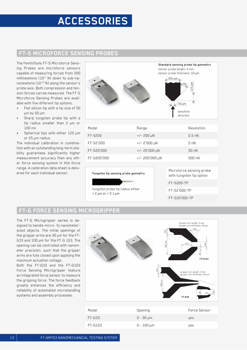
The FemtoTools FT-S Microforce Sens-ing Probes are microforce sensors capable of measuring forces from 200 millinewtons (10-1 N) down to sub-na-nonewtons (10-10 N) along the sensor’s probe axis. Both compression and ten-sion forces can be measured. The FT-S Microforce Sensing Probes are avail-able with five different tip options. • Flat silicon tip with a tip size of 50
µm by 50 µm• Sharp tungsten probe tip with a
tip radius smaller than 2 µm or 100 nm
• Spherical tips with either 125 µm or 25 µm radius
The individual calibration in combina-tion with an outstanding long-term sta-bility guarantees significantly higher measurement accuracy than any oth-er force sensing system in this force range. A calibration data sheet is deliv-ered for each individual sensor.
FT-s microForce sensing proBes
FT-g Force sensing microgripper
FT-S200 +/- 200 µN 0.5 nN
FT-S200-TP
FT-G33 0 - 30 µm yes
FT-S20’000 +/- 20’000 µN 50 nN
FT-S20’000-TP
FT-S200’000 +/- 200’000 µN 500 nN
FT-S2’000 +/- 2’000 µN 5 nN
FT-S2’000-TP
FT-G103 0 - 100 µm yes
Model Range Resolution
Microforce sensing probe with tungsten tip option
Model Opening Force Sensor
sensor probe length: 3 mmsensor probe thickness: 50 µm
125
µm
50 µm
300 µm
45°
sensitive direction
Standard sensing probe tip geometry
Tungsten tip sensing probe geometry
tungsten probe tip radius either ≤ 2 µm or ≤ 0.1 µm
sensor probe length: 3 mmsensor probe thickness: 50 µm
125
µm
50 µm
300 µm
45°
sensitive direction
Standard sensing probe tip geometry
Tungsten tip sensing probe geometry
tungsten probe tip radius either ≤ 2 µm or ≤ 0.1 µm
The FT-G Microgripper series is de-signed to handle micro- to nanometer-sized objects. The initial openings of the gripper arms are 30 µm for the FT-G33 and 100 µm for the FT-G 103. The opening can be controlled with nanom-eter precision, such that the gripper arms are fully closed upon applying the maximum actuation voltage.Both the FT-G33 and the FT-G103 Force Sensing Microgripper feature an integrated force sensor to measure the gripping force. The force feedback greatly enhances the efficiency and reliability of automated microhandling systems and assembly processes.
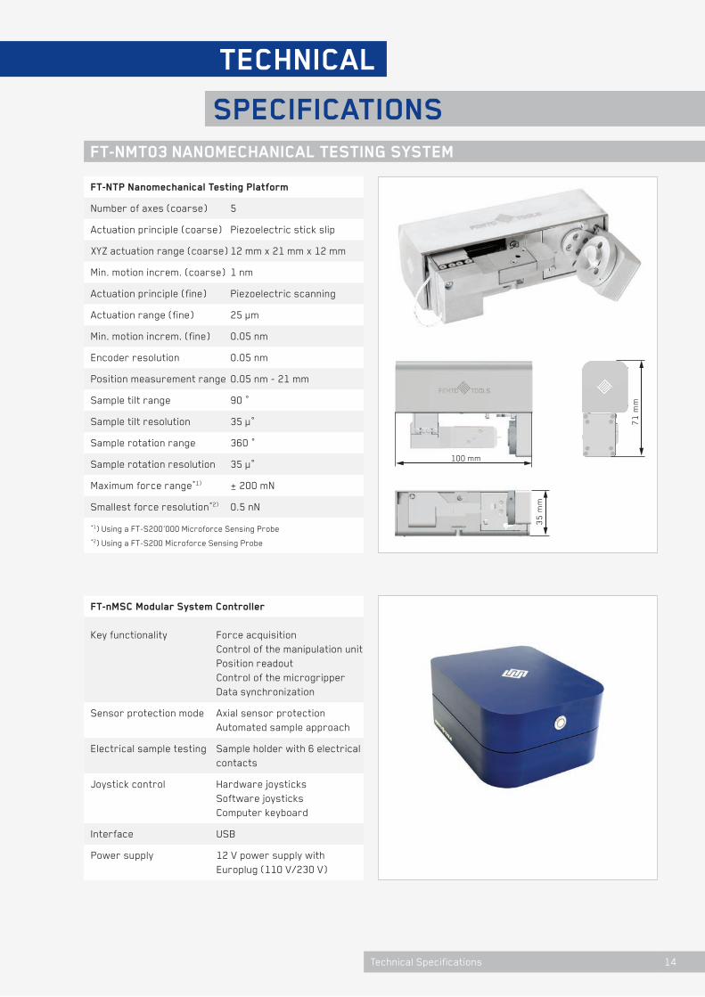
FT-nmT03 nanomechanical TesTing sysTem
Number of axes (coarse) 5
Key functionality Force acquisition Control of the manipulation unit Position readout Control of the microgripper Data synchronization
Actuation principle (fine) Piezoelectric scanning
Interface USB
Min. motion increm. (fine) 0.05 nm
Sample tilt resolution 35 µ°
XYZ actuation range (coarse) 12 mm x 21 mm x 12 mm
Electrical sample testing Sample holder with 6 electrical contacts
Position measurement range 0.05 nm - 21 mm
Sample rotation resolution 35 µ°
*1) Using a FT-S200’000 Microforce Sensing Probe *2) Using a FT-S200 Microforce Sensing Probe
Min. motion increm. (coarse) 1 nm
Joystick control Hardware joysticks Software joysticks Computer keyboard
Actuation range (fine) 25 µm
Power supply 12 V power supply with Europlug (110 V/230 V)
Sample tilt range 90 °
Maximum force range*1) ± 200 mN
Actuation principle (coarse) Piezoelectric stick slip
Sensor protection mode Axial sensor protection Automated sample approach
Encoder resolution 0.05 nm
Sample rotation range 360 °
FT-nTp nanomechanical Testing platform
FT-nmsc modular system controller
Technical
speciFicaTions
100 mm
35
mm
71
mm
Smallest force resolution*2) 0.5 nN
14Technical Specifications
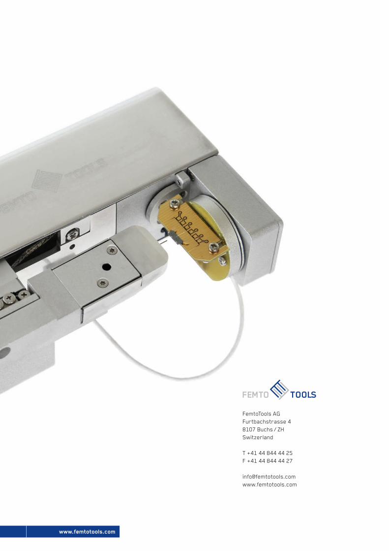
FemtoTools AGFurtbachstrasse 48107 Buchs / ZHSwitzerland
T +41 44 844 44 25F +41 44 844 44 27
www.femtotools.com
FEMTO TOOLS