Embed Size (px)
Citation preview
Integrated broadband Ce:YIG/Si Mach–Zehnderoptical isolators with over 100 nm tuning rangeDUANNI HUANG,1,*,† PAOLO PINTUS,1,† YUYA SHOJI,2 PAUL MORTON,3 TETSUYA MIZUMOTO,2
AND JOHN E. BOWERS1
1Department of Electrical and Computer Engineering, University of California, Santa Barbara, California 93106, USA2Department of Electrical and Electronic Engineering/FIRST, Tokyo Institute of Technology, Tokyo, Japan3Morton Photonics, 3301 Velvet Valley Dr., West Friendship, Maryland 21794, USA*Corresponding author: [email protected]
Received 14 August 2017; revised 29 October 2017; accepted 2 November 2017; posted 3 November 2017 (Doc. ID 304738);published 22 November 2017
We demonstrate integrated optical isolators with broadbandbehavior for the standard silicon-on-insulator platform.We achieve over 20 dB of optical isolation across 18 nmof optical bandwidth. The isolator is completely electricallycontrolled and does not require a permanent magnet.Furthermore, we demonstrate the ability to tune the centraloperating wavelength of the isolator across 100 nm, whichcovers the entire S + C telecom bands. These devices showpromise for integration in optical systems in which broad-band isolation is needed such as wavelength multiplexed sys-tems or optical sensors. © 2017 Optical Society of America
OCIS codes: (230.3240) Isolators; (230.3810) Magneto-optic
systems; (130.3120) Integrated optics devices.
https://doi.org/10.1364/OL.42.004901
Nonreciprocal optical devices [1] such as isolators and circula-tors are widely used in fiber optic communication systems,optical sensors, radio frequency photonics systems, and inter-connects. The rapid growth of silicon photonics and growingcomplexity of photonic integrated circuits (PICs) need inte-grated isolators to ensure stable, high-performance laser oper-ation. While considerable research effort has been performed touse dynamic modulation [2–4] or optical nonlinearities [5–7],the best results to date in terms of isolation ratio and opticalbandwidth (BW) have used the magneto-optic effect to breakreciprocity [8,9]. In particular, cerium substituted yttrium irongarnet (Ce:YIG) has been used due to its high Faraday rotation(θf � −4500 deg ∕cm) at 1550 nm [10]. Deposition of Ce:YIG directly onto silicon is a promising approach, but ischallenging due to the large thermal and lattice mismatch withsilicon [11–14]. Alternatively, wafer bonding circumvents theseissues and ensures optimal material quality, since the Ce:YIG isgrown on a lattice-matched substituted gadolinium galliumgarnet (SGGG) substrate [15–20]. While wafer-bonded ap-proaches generally operate for the transverse magnetic (TM)polarization of light, they can be integrated with a polarization
rotator to be compatible with typical semiconductor lasers,which emit in the transverse electric polarization [17].
Previously, we have demonstrated microring-based opticalisolators and circulators for silicon photonics with the waferbonding approach [18]. Due to the small footprint of the de-vices, we used an integrated electromagnet deposited on thedevice to provide the necessary magnetic fields in highly local-ized areas on a chip instead of packaging a bulky permanentmagnet. Additionally, the electromagnet can be used to tunethe operating wavelength of the device and reconfigure theorder of circulation of light through the circulator device [19].While we achieved up to 32 dB of optical isolation, the deviceis intrinsically narrowband due to the ring architecture [20].
In this Letter, we extend our approach to Mach–Zehnderinterferometer (MZI)-based isolators and demonstrate over20 dB of optical isolation across 18 nm of BW. MZI deviceshave broadband performance when properly designed with alarge free spectral range (FSR) [21]. By incorporating an inte-grated electromagnet instead of a permanent magnet, we alsounlock the ability to tune the center wavelength of the isolatorover 100 nm, a range that is only limited by the tuning range ofour laser. Tunability is important, as the operating wavelengthof a PIC should not be determined by the isolator. This tun-ability can also be used to adjust for temperature variation inthe operation of the PIC and maintain the central isolationwavelength.
The design of our isolator begins with optimization of thecross section of a magneto-optic waveguide using a finiteelement mode solver to provide a nonreciprocal phase shift(NRPS) effect between forward and backward propagatinglight [22,23]. Depicted in Fig. 1, the cross section consists ofCe:YIG bonded on a patterned silicon-on-insulator wafer. Thesilicon waveguide is 220 nm tall by 600 nm wide and supportsa single mode for the TM polarization. We directly bond theCe:YIG onto the waveguide and proceed to thin down theSGGG substrate to 10 μm using mechanical polishing tech-niques. Finally, Ti/Au microstrips are deposited on the backsideof the SGGG substrate to form the electromagnet. Further de-tails concerning the fabrication flow can be found in Ref. [20].
Letter Vol. 42, No. 23 / December 1 2017 / Optics Letters 4901
0146-9592/17/234901-04 Journal © 2017 Optical Society of America
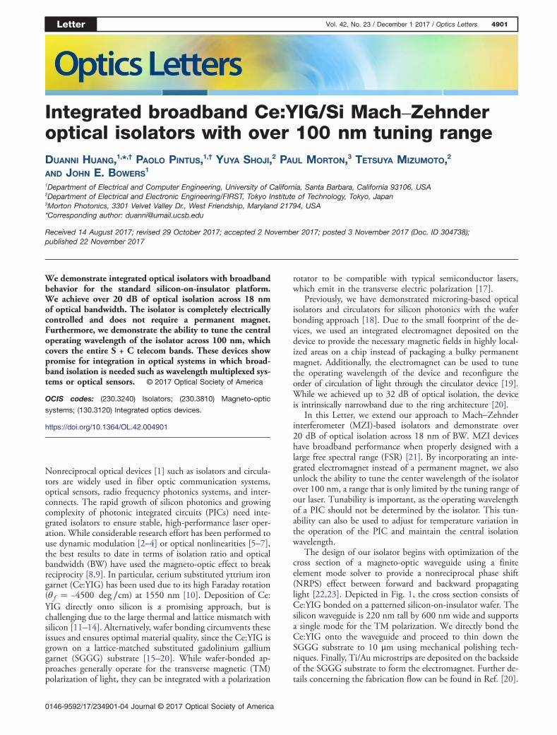
To achieve optical isolation using NRPS, we form an unbal-anced MZI, as shown in Fig. 2. Two electromagnets of equallength L are deposited on the arms and driven independentlywith opposite current polarity in a push–pull configuration.In this letter, we use directional couplers to split the lightand analyze transmission in the cross state (Port 1 → 4 and viceversa). 1 × 2 splitters and 3 × 2 couplers can be used instead.While the design in Fig. 2 can also be used as an optical cir-culator (Port 1 → 4 → 3 → 2 → 1), the wavelength depend-ence of the directional couplers prevents the device frombeing broadband. Adiabatic couplers are a possible option toensure 50:50 splitting over a wide wavelength range [24].In this Letter, we restrict the analysis of our device to an isolator,as the cross port of an MZI shows high extinction, regardless ofthe splitting ratio of the couplers if they are identical.
The optical path imbalance Δδ between the two arms is
Δδ � β · ΔL� β2L − β1L; (1)
where β is the phase constant of the waveguide when no mag-netic field is present, β1 and β2 are the phase constants in thetop and bottom arms, and ΔL is the geometrical path imbal-ance between the arms. When a current is injected through theelectromagnet, the phase constant is changed by�δβMO due to
the magneto-optic NRPS, as well as δβTH due to Joule heating[18]. The sign of the magneto-optic effect is dependent on thedirection of the magnetic field (and current), as well as thepropagation direction of light. Assuming equal and oppositecurrent I 1 and I2 in the electromagnets, we obtain the follow-ing for β1 and β2:
β1;forward � β − δβMO � δβTH; (2a)
β2;forward � β� δβMO � δβTH; (2b)
β1;backward � β� δβMO � δβTH; (2c)
β2;backward � β − δβMO � δβTH: (2d)
The thermal phase shift δβTH is the same for both arms ifΔL ≪ L, leaving only the magneto-optic effect to contributeto Δδ. Finally, to achieve optical isolation, we need to satisfythe following equations:
Δδforward � β · ΔL� 2δβMOL � 2πm; (3a)
Δδbackward � β · ΔL − 2δβMOL � 2πn� π: (3b)
This ensures that forward propagating light will interfere con-structively at the coupler, while backward propagating light willinterfere destructively. To minimize the size and, therefore, in-sertion loss of the device, we only consider m � n� 1. Thisselection results in δβMOL � π∕4, which determines the min-imal length of the magneto-optic section, which has higher lossthan standard silicon waveguides. From our simulations on thisstructure using a finite element-based mode solver [23], we ob-tain a conservative value δβMO � 0.834 mm−1 and β �8.826 μm−1 for the fundamental TM mode at 1550 nm.This sets our electromagnet length at L � 941 μm. The reasonfor a conservative estimate is due to Joule heating, which de-creases the magneto-optic effect [25]. In the absence of heating,δβMO can be as large as 2.294 mm−1, meaning L can be as smallas 342 μm, which could further reduce the loss of this device.
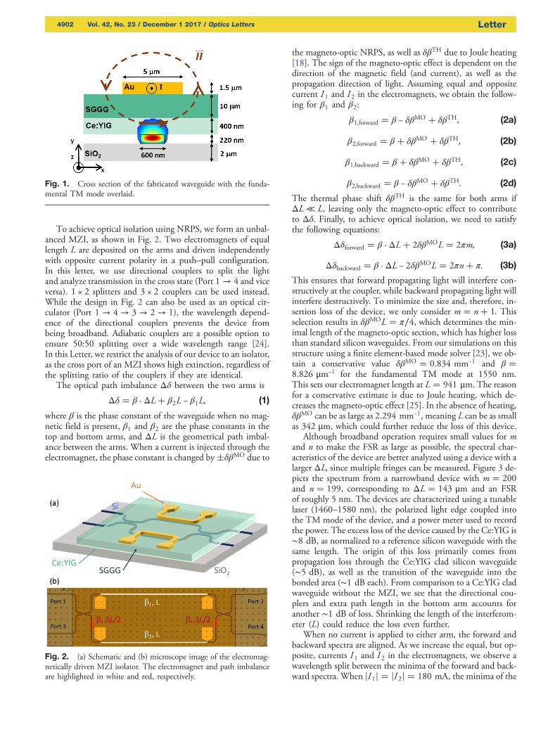
Although broadband operation requires small values for mand n to make the FSR as large as possible, the spectral char-acteristics of the device are better analyzed using a device with alarger ΔL, since multiple fringes can be measured. Figure 3 de-picts the spectrum from a narrowband device with m � 200and n � 199, corresponding to ΔL � 143 μm and an FSRof roughly 5 nm. The devices are characterized using a tunablelaser (1460–1580 nm), the polarized light edge coupled intothe TM mode of the device, and a power meter used to recordthe power. The excess loss of the device caused by the Ce:YIG is∼8 dB, as normalized to a reference silicon waveguide with thesame length. The origin of this loss primarily comes frompropagation loss through the Ce:YIG clad silicon waveguide(∼5 dB), as well as the transition of the waveguide into thebonded area (∼1 dB each). From comparison to a Ce:YIG cladwaveguide without the MZI, we see that the directional cou-plers and extra path length in the bottom arm accounts foranother ∼1 dB of loss. Shrinking the length of the interferom-eter (L) could reduce the loss even further.
When no current is applied to either arm, the forward andbackward spectra are aligned. As we increase the equal, but op-posite, currents I1 and I 2 in the electromagnets, we observe awavelength split between the minima of the forward and back-ward spectra. When jI1j � jI 2j � 180 mA, the minima of the
Fig. 1. Cross section of the fabricated waveguide with the funda-mental TM mode overlaid.
Fig. 2. (a) Schematic and (b) microscope image of the electromag-netically driven MZI isolator. The electromagnet and path imbalanceare highlighted in white and red, respectively.
4902 Vol. 42, No. 23 / December 1 2017 / Optics Letters Letter
backward spectra align with the maxima of the forward spectra,which results in the maximum optical isolation. Given the4 Ohm resistance of each microstrip, this corresponds to130 mW of power dissipated due to the Joule heating per mi-crostrip. Improvements on substrate removal to thin the SGGGeven further will decrease the current required, since magneticfield strength is inversely proportional with substrate thickness.Decreasing the drive current will also help mitigate electro-migration as a failure mechanism in the microstrip.
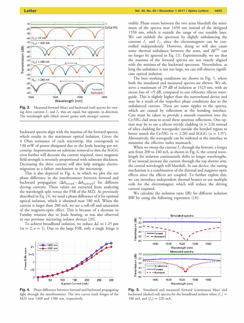
This is also depicted in Fig. 4, in which we plot the netphase difference in the interferometer between forward andbackward propagation (Δδforward − Δδbackward) for differentdriving currents. These values are extracted from analyzingthe wavelength split versus the FSR of the MZI. As previouslydescribed in Eq. (3), we need a phase difference of π for optimaloptical isolation, which is obtained near 180 mA. When thecurrent is larger than 280 mA, we see a roll-off and saturationof the magneto-optic effect. This is because of a decrease inFaraday rotation due to Joule heating, as was also observedin our previous microring isolator devices [20].
To achieve broadband isolation, we reduce ΔL to 1.25 μm(m � 2; n � 1). Due to the large FSR, only a single fringe is
visible. Phase errors between the two arms blueshift the mini-mum of the spectra near 1450 nm instead of the designed1550 nm, which is outside the range of our tunable laser.We can redshift the spectrum by slightly unbalancing thecurrents I 1 and I 2, since the electromagnets can be con-trolled independently. However, doing so will also causesome thermal unbalance between the arms, and δβTH canno longer be ignored in Eq. (2). Experimentally, we see thatthe maxima of the forward spectra are not exactly alignedwith the minima of the backward spectrum. Nevertheless, aslong the unbalance is not too large, we can still observe signifi-cant optical isolation.
The best working conditions are shown in Fig. 5, whereboth the simulated and measured spectra are shown. We ob-serve a maximum of 29 dB of isolation at 1523 nm, with anexcess loss of ∼9 dB, compared to our reference silicon wave-guide. This is slightly higher than the narrowband device andmay be a result of the imperfect phase conditions due to theunbalanced current. There are some ripples in the spectra,which are caused by reflections at the bonding interface.Care must be taken to provide a smooth transition into theCe:YIG clad areas to avoid these spurious reflections. One op-tion may be to use a silicon nitride cladding (n � 2.0) insteadof silica cladding for waveguides outside the bonded region tobetter match the Ce:YIG (n � 2.20) and SGGG (n � 1.97).Alternatively, the waveguide can be widened at the interface tominimize the effective index mismatch.
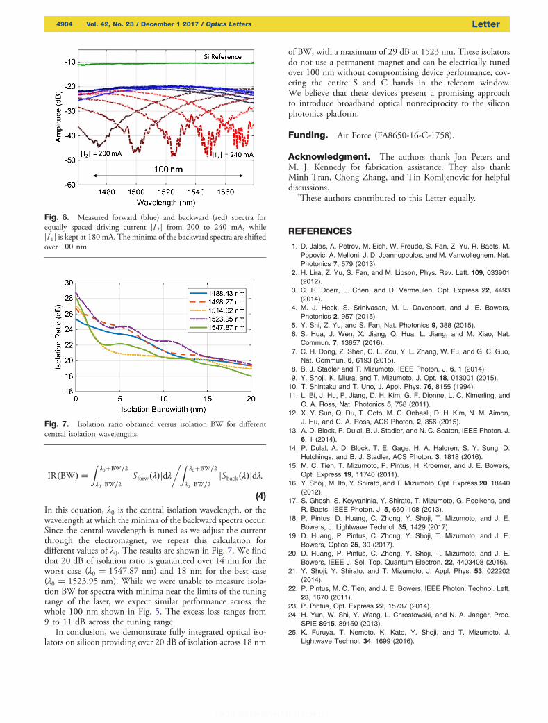
When we sweep the current I2 through the bottom, a longerarm from 200 to 240 mA, as shown in Fig. 6, the central wave-length for isolation continuously shifts to longer wavelengths.If we instead increase the current through the top shorter arm,the central wavelength will blueshift. In our device, the tuningmechanism is a combination of the thermal and magneto-opticeffects since the effects are coupled. To further exploit this,we can introduce independent thermal heaters or use multiplecoils for the electromagnet which will reduce the drivingcurrent required.
We calculate the isolation ratio (IR) for different isolationBW by using the following expression [18]:
Fig. 3. Measured forward (blue) and backward (red) spectra for vary-ing drive currents I1 and I 2 that are equal, but opposite, in direction.The wavelength split (black arrow) grows with stronger current.
Fig. 4. Phase difference between forward and backward propagatinglight through the interferometer. The two curves track fringes of theMZI near 1460 and 1580 nm, respectively.
Fig. 5. Simulated and measured forward (continuous blue) andbackward (dashed red) spectra for the broadband isolator when jI1j �180 mA and jI 2j � 220 mA.
Letter Vol. 42, No. 23 / December 1 2017 / Optics Letters 4903
IR�BW� �Z
λ0�BW∕2
λ0−BW∕2jS forw�λ�jdλ
�Zλ0�BW∕2
λ0−BW∕2jSback�λ�jdλ:
(4)
In this equation, λ0 is the central isolation wavelength, or thewavelength at which the minima of the backward spectra occur.Since the central wavelength is tuned as we adjust the currentthrough the electromagnet, we repeat this calculation fordifferent values of λ0. The results are shown in Fig. 7. We findthat 20 dB of isolation ratio is guaranteed over 14 nm for theworst case (λ0 � 1547.87 nm) and 18 nm for the best case(λ0 � 1523.95 nm). While we were unable to measure isola-tion BW for spectra with minima near the limits of the tuningrange of the laser, we expect similar performance across thewhole 100 nm shown in Fig. 5. The excess loss ranges from9 to 11 dB across the tuning range.
In conclusion, we demonstrate fully integrated optical iso-lators on silicon providing over 20 dB of isolation across 18 nm
of BW, with a maximum of 29 dB at 1523 nm. These isolatorsdo not use a permanent magnet and can be electrically tunedover 100 nm without compromising device performance, cov-ering the entire S and C bands in the telecom window.We believe that these devices present a promising approachto introduce broadband optical nonreciprocity to the siliconphotonics platform.
Funding. Air Force (FA8650-16-C-1758).
Acknowledgment. The authors thank Jon Peters andM. J. Kennedy for fabrication assistance. They also thankMinh Tran, Chong Zhang, and Tin Komljenovic for helpfuldiscussions.
†These authors contributed to this Letter equally.
REFERENCES
1. D. Jalas, A. Petrov, M. Eich, W. Freude, S. Fan, Z. Yu, R. Baets, M.Popovic, A. Melloni, J. D. Joannopoulos, and M. Vanwolleghem, Nat.Photonics 7, 579 (2013).
2. H. Lira, Z. Yu, S. Fan, and M. Lipson, Phys. Rev. Lett. 109, 033901(2012).
3. C. R. Doerr, L. Chen, and D. Vermeulen, Opt. Express 22, 4493(2014).
4. M. J. Heck, S. Srinivasan, M. L. Davenport, and J. E. Bowers,Photonics 2, 957 (2015).
5. Y. Shi, Z. Yu, and S. Fan, Nat. Photonics 9, 388 (2015).6. S. Hua, J. Wen, X. Jiang, Q. Hua, L. Jiang, and M. Xiao, Nat.
Commun. 7, 13657 (2016).7. C. H. Dong, Z. Shen, C. L. Zou, Y. L. Zhang, W. Fu, and G. C. Guo,
Nat. Commun. 6, 6193 (2015).8. B. J. Stadler and T. Mizumoto, IEEE Photon. J. 6, 1 (2014).9. Y. Shoji, K. Miura, and T. Mizumoto, J. Opt. 18, 013001 (2015).10. T. Shintaku and T. Uno, J. Appl. Phys. 76, 8155 (1994).11. L. Bi, J. Hu, P. Jiang, D. H. Kim, G. F. Dionne, L. C. Kimerling, and
C. A. Ross, Nat. Photonics 5, 758 (2011).12. X. Y. Sun, Q. Du, T. Goto, M. C. Onbasli, D. H. Kim, N. M. Aimon,
J. Hu, and C. A. Ross, ACS Photon. 2, 856 (2015).13. A. D. Block, P. Dulal, B. J. Stadler, and N. C. Seaton, IEEE Photon. J.
6, 1 (2014).14. P. Dulal, A. D. Block, T. E. Gage, H. A. Haldren, S. Y. Sung, D.
Hutchings, and B. J. Stadler, ACS Photon. 3, 1818 (2016).15. M. C. Tien, T. Mizumoto, P. Pintus, H. Kroemer, and J. E. Bowers,
Opt. Express 19, 11740 (2011).16. Y. Shoji, M. Ito, Y. Shirato, and T. Mizumoto, Opt. Express 20, 18440
(2012).17. S. Ghosh, S. Keyvaninia, Y. Shirato, T. Mizumoto, G. Roelkens, and
R. Baets, IEEE Photon. J. 5, 6601108 (2013).18. P. Pintus, D. Huang, C. Zhong, Y. Shoji, T. Mizumoto, and J. E.
Bowers, J. Lightwave Technol. 35, 1429 (2017).19. D. Huang, P. Pintus, C. Zhong, Y. Shoji, T. Mizumoto, and J. E.
Bowers, Optica 25, 30 (2017).20. D. Huang, P. Pintus, C. Zhong, Y. Shoji, T. Mizumoto, and J. E.
Bowers, IEEE J. Sel. Top. Quantum Electron. 22, 4403408 (2016).21. Y. Shoji, Y. Shirato, and T. Mizumoto, J. Appl. Phys. 53, 022202
(2014).22. P. Pintus, M. C. Tien, and J. E. Bowers, IEEE Photon. Technol. Lett.
23, 1670 (2011).23. P. Pintus, Opt. Express 22, 15737 (2014).24. H. Yun, W. Shi, Y. Wang, L. Chrostowski, and N. A. Jaeger, Proc.
SPIE 8915, 89150 (2013).25. K. Furuya, T. Nemoto, K. Kato, Y. Shoji, and T. Mizumoto, J.
Lightwave Technol. 34, 1699 (2016).
Fig. 6. Measured forward (blue) and backward (red) spectra forequally spaced driving current jI 2j from 200 to 240 mA, whilejI 1j is kept at 180 mA. The minima of the backward spectra are shiftedover 100 nm.
Fig. 7. Isolation ratio obtained versus isolation BW for differentcentral isolation wavelengths.
4904 Vol. 42, No. 23 / December 1 2017 / Optics Letters Letter