Embed Size (px)
Citation preview
ECEN5807, Spring 2005
ECEN5807Modeling and Control of Power Electronic Systems
• Instructor: Dragan Maksimovic• Office: EE1B71, phone: 303-492-4863, fax: 303-492-2758• E-mail: [email protected]• Office hours: Monday, Tuesday, Friday 9:30-10:30am
• Course web site:• http://ece.colorado.edu/~ecen5807• Announcements, course materials, assignments, solutions
• Textbook:• Erickson and Maksimovic, Fundamentals of Power Electronics, 2nd
edition, Kluwer 2001• On-line course lectures (Tegrity system):
• Accessible through the CAETE site: http://caeteport.colorado.edu
ECEN5807, Spring 2005
Assignments
• Weekly homeworks (11-12 total), 35% of the grade• Midterm exam (open book/notes, take-home), 25% of the grade• Final exam (comprehensive, open book/notes, take-home), 40% of the
grade• All assignments, due dates, and solutions will be posted on the course
web site• For homework assignments, the due date for off-campus students is
(postmarked) one week after the due date published for on-campus students
• Homework assignments and the final exam may require use of a Spice simulator (free student version of PSpice is sufficient)
ECEN5807, Spring 2005
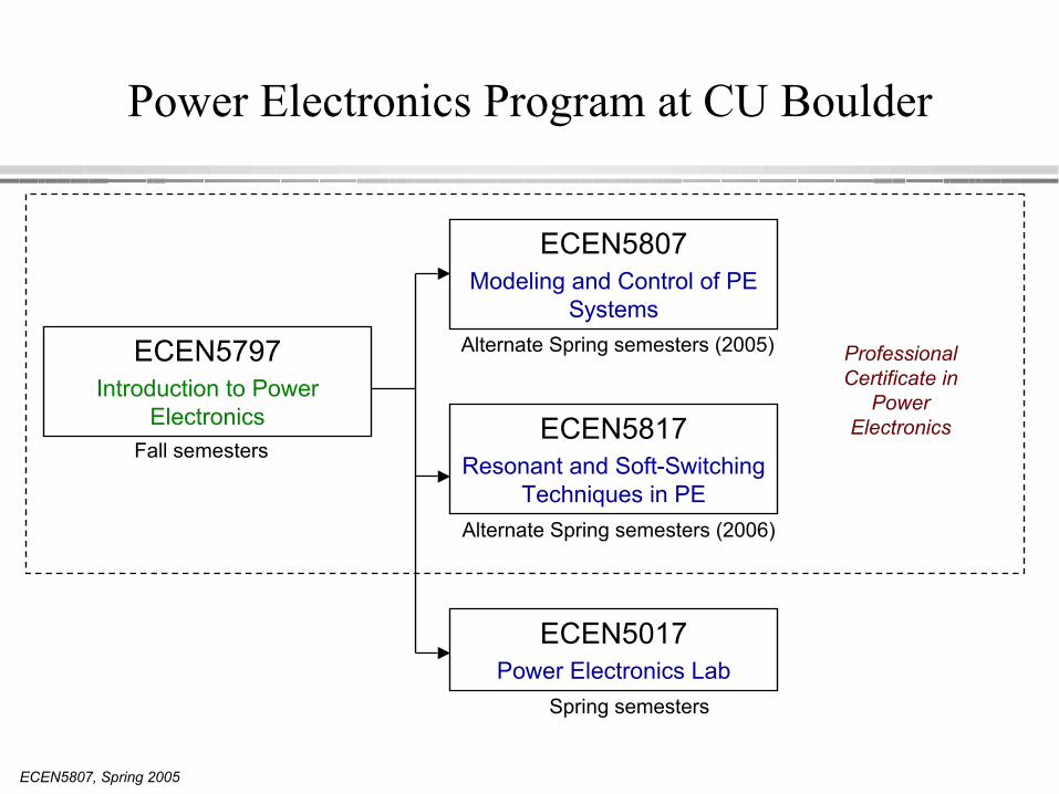
Power Electronics Program at CU Boulder
ECEN5797Introduction to Power
Electronics
ECEN5807Modeling and Control of PE
Systems
ECEN5817Resonant and Soft-Switching
Techniques in PE
ECEN5017Power Electronics Lab
Fall semesters
Spring semesters
Alternate Spring semesters (2006)
Alternate Spring semesters (2005) Professional Certificate in
Power Electronics
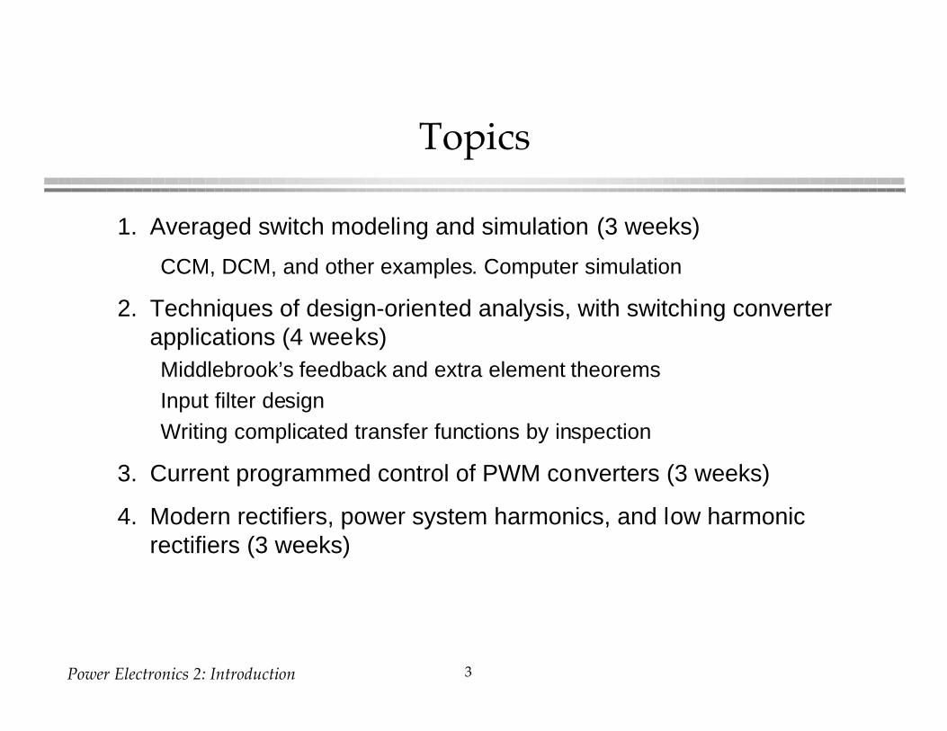
Power Electronics 2: Introduction 3
Topics
1. Averaged switch modeling and simulation (3 weeks)
CCM, DCM, and other examples. Computer simulation
2. Techniques of design-oriented analysis, with switching converterapplications (4 weeks)Middlebrook’s feedback and extra element theoremsInput filter designWriting complicated transfer functions by inspection
3. Current programmed control of PWM converters (3 weeks)
4. Modern rectifiers, power system harmonics, and low harmonicrectifiers (3 weeks)
Power Electronics 2: Introduction 4
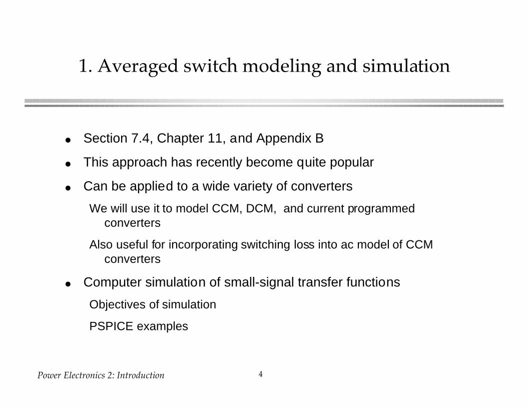
1. Averaged switch modeling and simulation
l Section 7.4, Chapter 11, and Appendix B
l This approach has recently become quite popular
l Can be applied to a wide variety of converters
We will use it to model CCM, DCM, and current programmedconverters
Also useful for incorporating switching loss into ac model of CCMconverters
l Computer simulation of small-signal transfer functions
Objectives of simulation
PSPICE examples
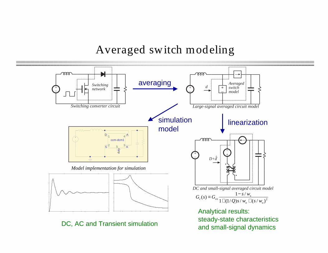
Averaged switch modeling
+–
Switching converter circuit
Switchingnetwork +
–+–
Large-signal averaged circuit model
Averagedswitchmodel
d
+–
+–
DC and small-signal averaged circuit model
D+d
2)/(/)/1(1
/1)(
oo
scoc wswsQ
wsGsG
++−=
1D
2S
3K
4A
5
duty
ccm-dcm1+
-
DC, AC and Transient simulation
Model implementation for simulation
simulationmodel
linearization
Analytical results:steady-state characteristicsand small-signal dynamics
averaging
Power Electronics 2: Introduction
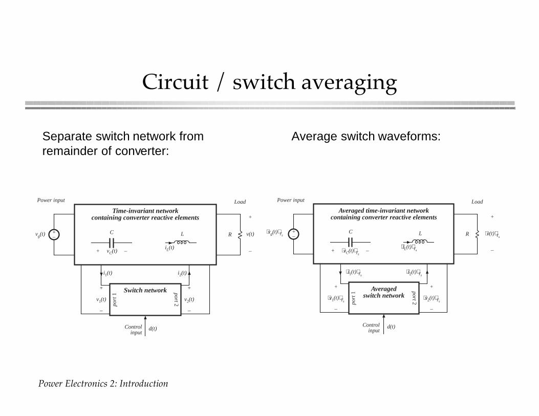
Circuit / switch averaging
+–
Time-invariant networkcontaining converter reactive elements
C L
+ vC(t) –iL(t)
R
+
v(t)
–
vg(t)
Power input Load
Switch network
po
rt 1
po
rt 2
d(t)Controlinput
+
v1(t)
–
+
v2(t)
–
i1(t) i2(t)
+–
Averaged time-invariant networkcontaining converter reactive elements
C L
+ ⟨vC(t)⟩Ts –
⟨iL(t)⟩Ts
R
+
⟨v(t)⟩Ts
–
⟨vg(t)⟩Ts
Power input Load
Averagedswitch network
po
rt 1
po
rt 2
d(t)Controlinput
+
⟨v2(t)⟩Ts
–
⟨i1(t)⟩Ts⟨i2(t)⟩Ts
+
⟨v1(t)⟩Ts
–
Separate switch network fromremainder of converter:
Average switch waveforms:
Power Electronics 2: Introduction 7
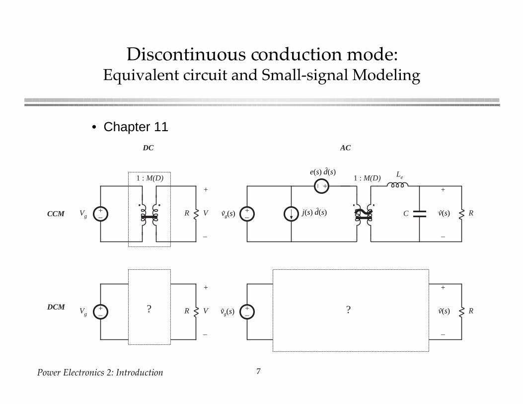
Discontinuous conduction mode:Equivalent circuit and Small-signal Modeling
DC
CCM
DCM
+–
1 : M(D)
Vg R
+
V
–
+–Vg R
+
V
–
+–
+– 1 : M(D) Le
C R
+
–
v(s)
e(s) d(s)
j(s) d(s)
AC
+– Rvg(s)
+
–
v(s)
vg(s)
??
• Chapter 11
Power Electronics 2: Introduction 8
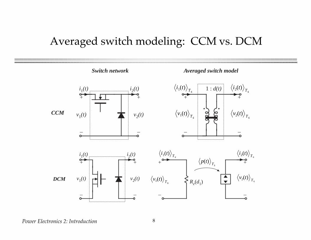
Averaged switch modeling: CCM vs. DCM
+
–
1 : d(t)i1(t) Tsi2(t) Ts
+
–
v2(t) Tsv1(t) Ts
Averaged switch modelSwitch network
CCM
+
v2(t)
–
+
v1(t)
–
i1(t) i2(t)
i2(t) Ts
+
–
v2(t) Tsv1(t) Ts
i1(t) Ts
Re(d1)
+
–
DCM
+
v2(t)
–
+
v1(t)
–
i1(t) i2(t)p(t)
Ts
Power Electronics 2: Introduction 9
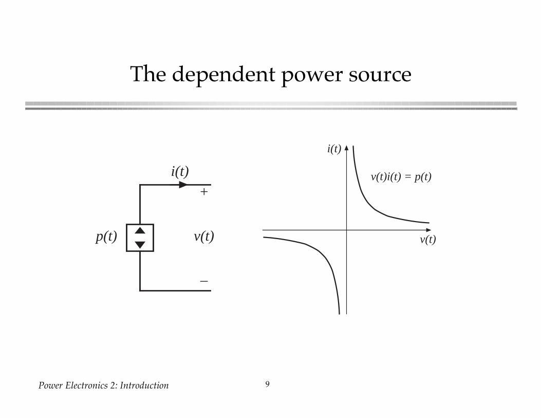
The dependent power source
p(t)
+
v(t)
–
i(t) v(t)i(t) = p(t)
v(t)
i(t)
Power Electronics 2: Introduction 10
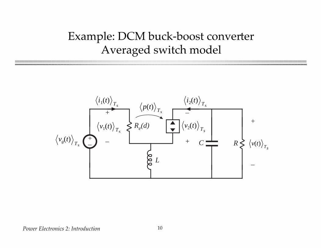
Example: DCM buck-boost converterAveraged switch model
i2(t) Ts
v2(t) Tsv1(t) Ts
i1(t) Ts
Re(d)
+–
L
C R
+
–
+
–
–
+ v(t)Ts
vg(t) Ts
p(t)Ts
Power Electronics 2: Introduction 11
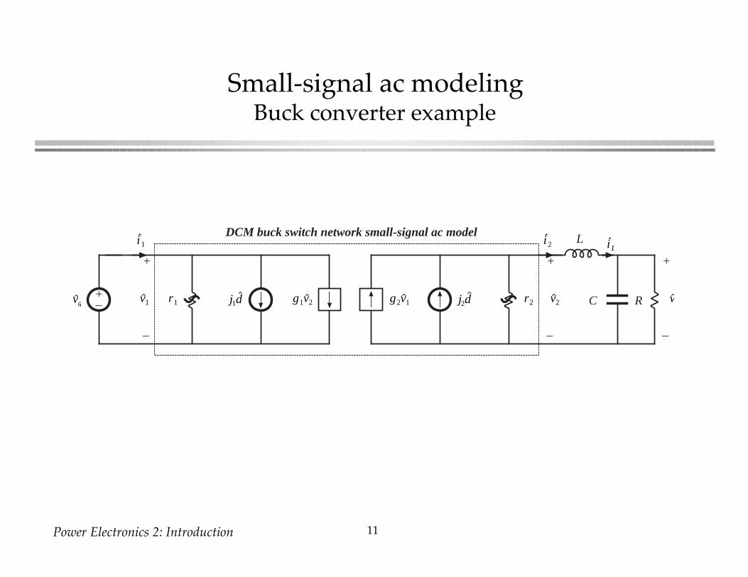
Small-signal ac modelingBuck converter example
+
–
+– v1 r1 j1d g1v2
i1
g2v1 j2d r2
i2
v2
+
–
L
C R
DCM buck switch network small-signal ac model
+
–
vg v
iL
Power Electronics 2: Introduction 12
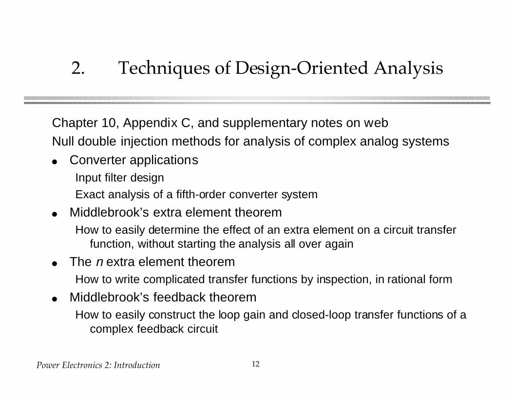
2. Techniques of Design-Oriented Analysis
Chapter 10, Appendix C, and supplementary notes on webNull double injection methods for analysis of complex analog systems
l Converter applicationsInput filter designExact analysis of a fifth-order converter system
l Middlebrook’s extra element theoremHow to easily determine the effect of an extra element on a circuit transfer
function, without starting the analysis all over again
l The n extra element theoremHow to write complicated transfer functions by inspection, in rational form
l Middlebrook’s feedback theoremHow to easily construct the loop gain and closed-loop transfer functions of a
complex feedback circuit
Power Electronics 2: Introduction 13
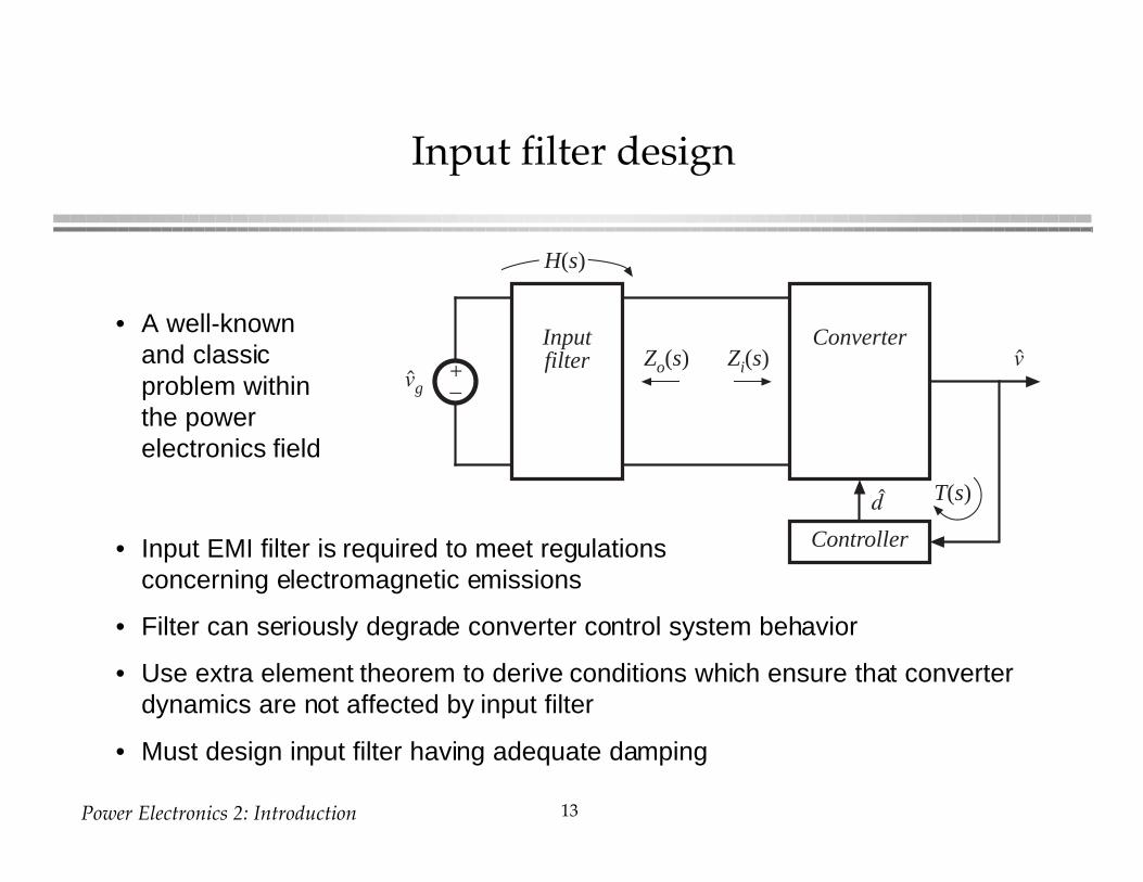
Input filter design
• Filter can seriously degrade converter control system behavior
• Use extra element theorem to derive conditions which ensure that converterdynamics are not affected by input filter
• Must design input filter having adequate damping
• Input EMI filter is required to meet regulationsconcerning electromagnetic emissions
• A well-knownand classicproblem withinthe powerelectronics field
+–
Inputfilter
Converter
T(s)
Controller
vg
Zo(s) Zi(s)
H(s)
d
v
Power Electronics 2: Introduction 14
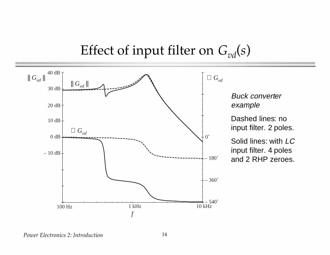
Effect of input filter on Gvd(s)
f
|| Gvd || ∠ Gvd
0˚
– 360˚
– 540˚
0 dB
– 10 dB
20 dB
30 dB
100 Hz
40 dB
1 kHz 10 kHz
– 180˚
10 dB
|| Gvd ||
∠ Gvd
Buck converterexample
Dashed lines: noinput filter. 2 poles.
Solid lines: with LCinput filter. 4 polesand 2 RHP zeroes.
Power Electronics 2, Spring 2003
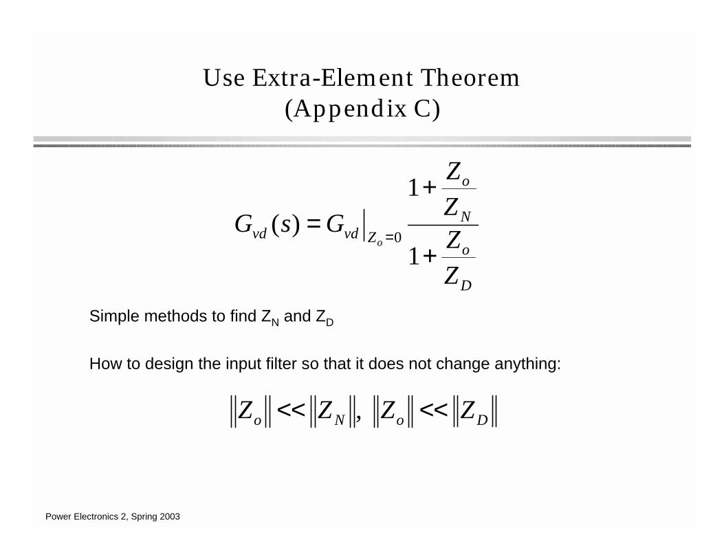
Use Extra-Element Theorem(Appendix C)
Simple methods to find ZN and ZD
How to design the input filter so that it does not change anything:
D
o
N
o
Zvdvd
Z
ZZ
Z
GsGo
+
+=
=1
1
)(0
, DoNo ZZZZ <<<<
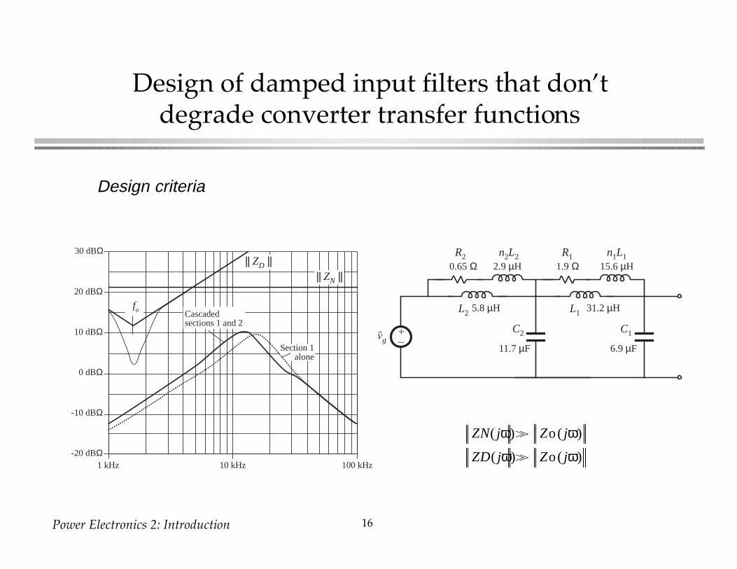
Power Electronics 2: Introduction 16
Design of damped input filters that donÕtdegrade converter transfer functions
-20 dBΩ
-10 dBΩ
0 dBΩ
10 dBΩ
20 dBΩ
1 kHz 10 kHz 100 kHz
Section 1alone
Cascadedsections 1 and 2
30 dBΩ
|| ZN |||| ZD ||
fo
+–vg
L1
n1L1R1
C1
L2
n2L2R2
C2
6.9 µF
31.2 µH
15.6 µH1.9 Ω0.65 Ω 2.9 µH
5.8 µH
11.7 µF
Design criteria
derived via
ExtraElement theorem:
Two-section
da
mped input filterdesign:
ZN( jω)> Zo ( jω)
ZD( jω)> Zo ( jω)
Power Electronics 2: Introduction 17
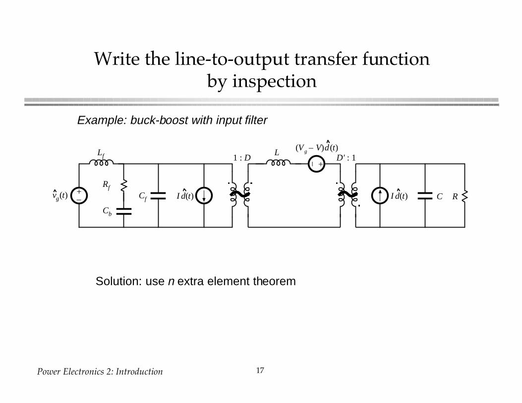
Write the line-to-output transfer functionby inspection
+–
+–
L
RC
1 : D D' : 1Lf
Rf
Cf
Cb
vg(t) I d(t)
(Vg – V)d(t)
I d(t)
Solution: use n extra element theorem
Example: buck-boost with input filter
Power Electronics 2: Introduction 18
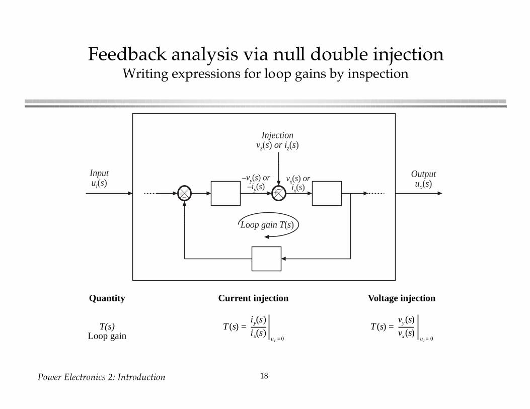
Feedback analysis via null double injectionWriting expressions for loop gains by inspection
–vy(s) or–iy(s)+– +–
Inputui(s)
Outputuo(s)
Loop gain T(s)
Injectionvz(s) or iz(s)
vx(s) orix(s)
Quantity Current injection Voltage injection
T(s)Loop gain
T (s) =iy(s)
ix(s)ui = 0
T (s) =vy(s)
vx(s) ui = 0
Power Electronics 2: Introduction 19
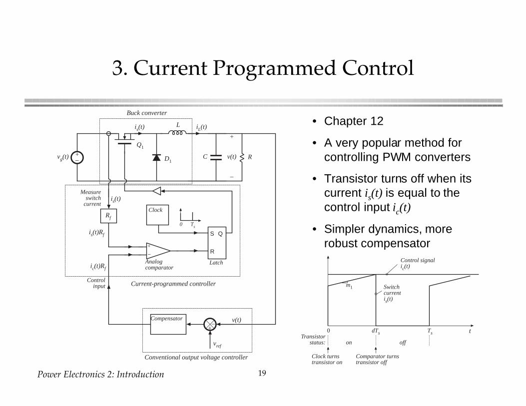
3. Current Programmed Control
+–
Buck converter
Current-programmed controller
Rvg(t)
is(t)
+
v(t)
–
iL(t)
Q1
L
CD1
+
–
Analogcomparator
Latch
Ts0
S
R
Q
Clock
is(t)
Rf
Measureswitch
current
is(t)Rf
Controlinput
ic(t)Rf
–+
vref
v(t)Compensator
Conventional output voltage controller
• Chapter 12
• A very popular method forcontrolling PWM converters
• Transistor turns off when itscurrent is(t) is equal to thecontrol input ic(t)
• Simpler dynamics, morerobust compensator
Switchcurrentis(t)
Control signalic(t)
m1
t0 dTs Ts
on offTransistor
status:
Clock turnstransistor on
Comparator turnstransistor off
Power Electronics 2: Introduction 20
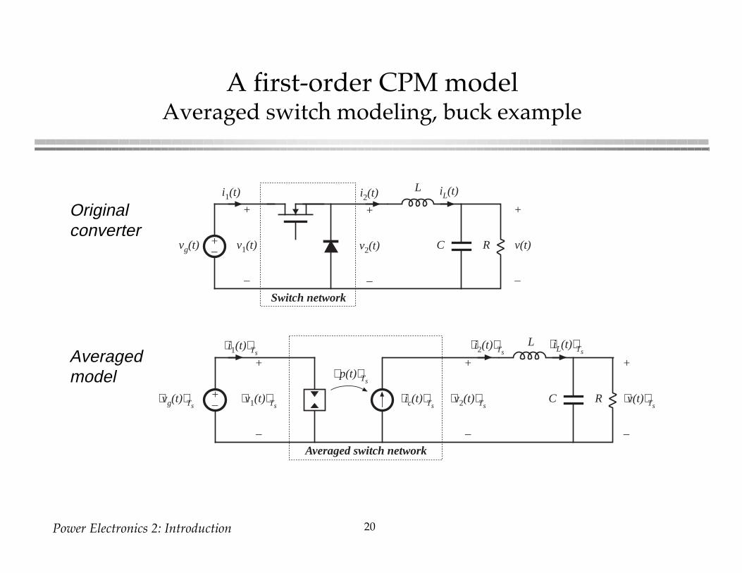
A first-order CPM modelAveraged switch modeling, buck example
+–
L
C R
+
v(t)
–
vg(t)
iL(t)
+
v2(t)
–
i1(t) i2(t)
Switch network
+
v1(t)
–
+–
L
C R
+
⟨v(t)⟩Ts
–
⟨vg(t)⟩Ts
⟨iL(t)⟩Ts
+
⟨v2(t)⟩Ts
–
⟨i1(t)⟩Ts⟨i2(t)⟩Ts
Averaged switch network
+
⟨v1(t)⟩Ts
–
⟨ic(t)⟩Ts
⟨ p(t)⟩Ts
Originalconverter
Averagedmodel
Power Electronics 2: Introduction 21
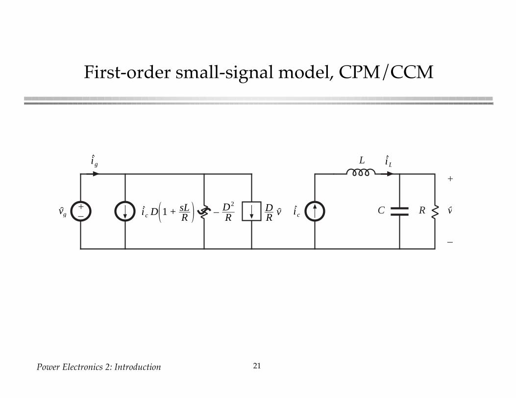
First-order small-signal model, CPM/CCM
+–
L
C R
+
–
vg ic v– D2
RDR
vic D 1 + sLR
ig iL
Power Electronics 2: Introduction 22
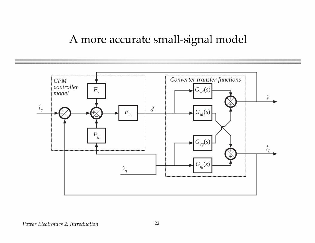
A more accurate small-signal model
+–+– –ic Fm
CPMcontrollermodel
d
Gvd(s)
Gid(s)
Gvg(s)
Gig(s)
++
++
v
iL
vg
Converter transfer functions
Fv
Fg
Power Electronics 2: Introduction 23
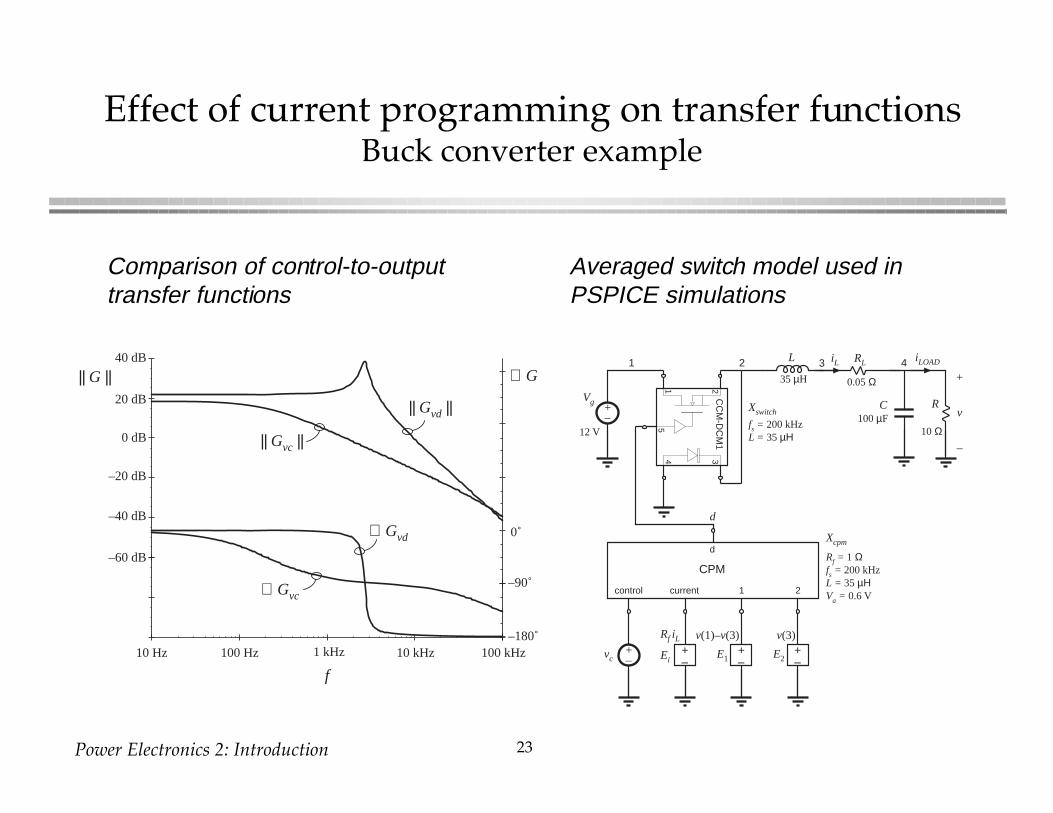
Effect of current programming on transfer functionsBuck converter example
|| Gvd ||
∠ Gvd
f
0˚
–90˚
–180˚
∠ G
–20 dB
–40 dB
0 dB
20 dB
40 dB
10 Hz 100 Hz 10 kHz 100 kHz1 kHz
|| G ||
–60 dB
|| Gvc ||
∠ Gvc
21
345
CC
M-D
CM
1
+–
+–
35 µH
100 µF
Vg
12 V
L
C R
vc
+
v
–
iLOAD
CPM
control current 1 2
d
+–
+–
+–
iL RL1 2 3 4
d
Rf iL v(1)–v(3) v(3)
0.05 Ω
10 Ω
Rf = 1 Ωfs = 200 kHzL = 35 µΗVa = 0.6 V
Xcpm
Xswitch
fs = 200 kHzL = 35 µΗ
EiE1 E2
Comparison of control-to-outputtransfer functions
Averaged switch model used inPSPICE simulations
Power Electronics 2: Introduction 24
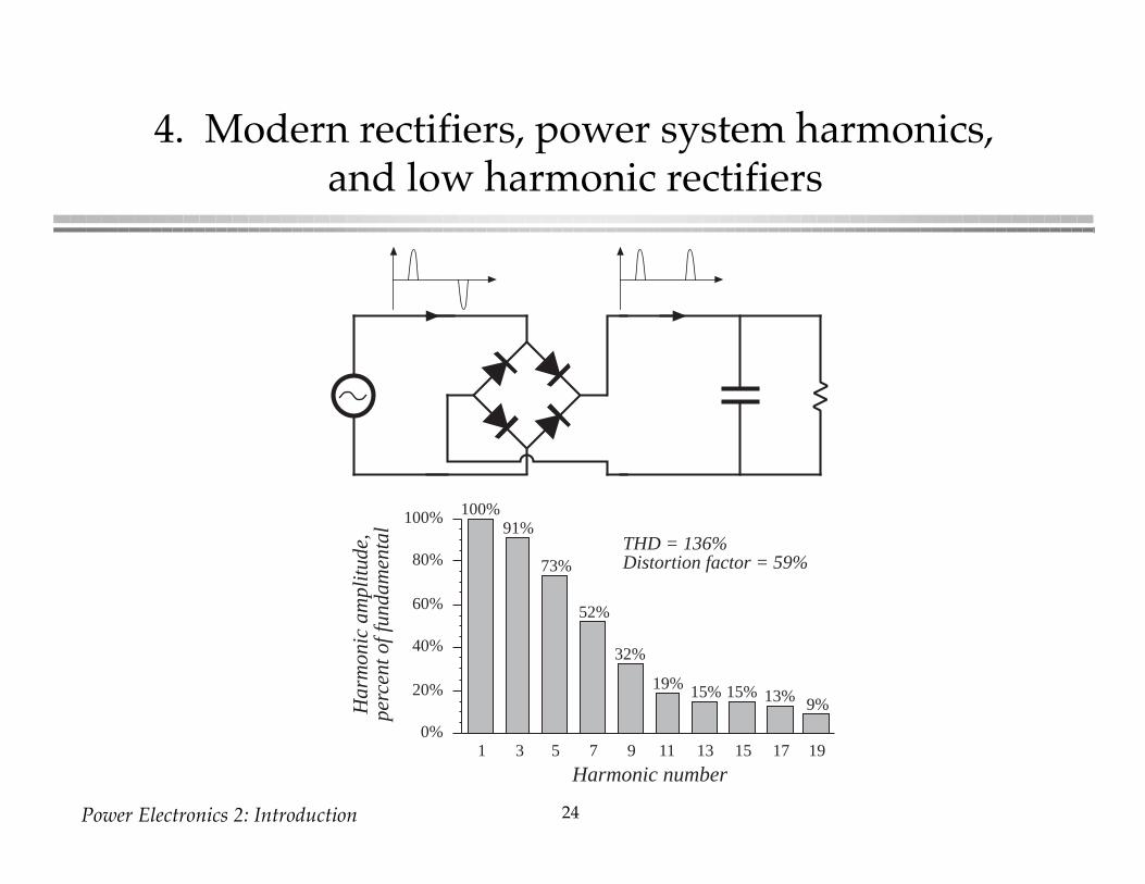
4. Modern rectifiers, power system harmonics,and low harmonic rectifiers
100%91%
73%
52%
32%
19% 15% 15%13% 9%
0%
20%
40%
60%
80%
100%
1 3 5 7 9 11 13 15 17 19
Harmonic number
Ha
rmo
nic
am
plit
ud
e,
pe
rce
nt o
f fu
nd
am
en
tal
THD = 136%Distortion factor = 59%
Power Electronics 2: Introduction 25
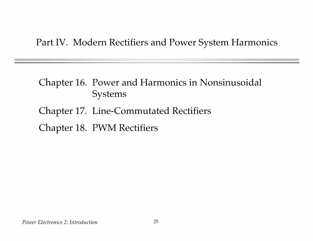
Part IV. Modern Rectifiers and Power System Harmonics
Chapter 16. Power and Harmonics in NonsinusoidalSystems
Chapter 17. Line-Commutated Rectifiers
Chapter 18. PWM Rectifiers
Power Electronics 2: Introduction 26
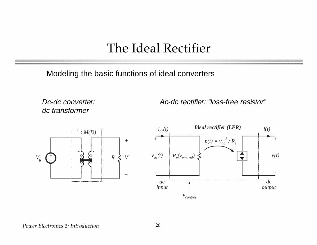
The Ideal Rectifier
+–
1 : M(D)
Vg R
+
V
–
Re(vcontrol)
+
–
vac(t)
iac(t)
vcontrol
v(t)
i(t)
+
–
p(t) = vac2 / Re
Ideal rectifier (LFR)
acinput
dcoutput
Modeling the basic functions of ideal converters
Dc-dc converter:dc transformer
Ac-dc rectifier: “loss-free resistor”
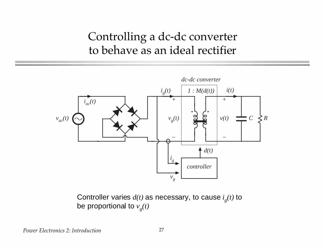
Power Electronics 2: Introduction 27
Controlling a dc-dc converterto behave as an ideal rectifier
1 : M(d(t))
dc-dc converter
controller
d(t)
Rvac(t)
iac(t)+
vg(t)
–
ig(t)
ig
vg
+
v(t)
–
i(t)
C
Controller varies d(t) as necessary, to cause ig(t) tobe proportional to vg(t)
Power Electronics 2: Introduction 28
A complete dc power supply system
boost converter
wide-bandwidth input current controller
vac(t)
iac(t)+
vg(t)
–
ig(t)
ig(t)vg(t)
+
vC(t)
–
i2(t)
Q1
L
C
D1
vcontrol(t)
multiplier X
+–vref1(t)
= kx vg(t) vcontrol(t)
Rsva(t)
Gc(s)
PWM
compensator
verr(t)
DC–DCConverter load
+
v(t)
–
i(t)
d(t)
+–compensatorand modulator
vref3
wide-bandwidth output voltage controller
+–compensatorvref2
low-bandwidth energy-storage capacitor voltage controller
vC(t)
v(t)
Power Electronics 2: Introduction
Rectifier modeling, design, and control
• Basics of power system harmonics. Power in nonsinusoidalsystems. (Chapter 16)
• Behavior of conventional diode rectifiers. Conventional harmonicmitigation techniques: harmonic trap filters, and polyphasetransformer connections. (Chapter 17)
• Steady-state design of low-harmonic PWM rectifiers. Controltechniques for PWM rectifiers. Use of small-signal models to designcontrol systems of PWM rectifiers. RMS calculations for doubly-modulated waveforms. Energy storage, and low-frequencywaveforms in single-phase low-harmonic rectifier systems. (Chapter18)
Power Electronics 2: Introduction
Next lecture
l Begin with circuit averaging and averaged switch modeling
l Assignment: Read Section 7.4


![Intro to parallel and series/parallel HEV architectures ...ecee.colorado.edu/~ecen5017/lectures/CU/L12_slides.pdf · Intro to parallel and series/parallel HEV ... time [sec] Step](https://img.pdfslide.net/doc/110x75/5ffdaa80f8451c652b521e2e/intro-to-parallel-and-seriesparallel-hev-architectures-ecee-ecen5017lecturescul12slidespdf.jpg)