Embed Size (px)
Citation preview
Introduction to Embedded ComputingSystems 2
This chapter begins with a brief overview of embedded computing systems in
Sect. 2.1, taking into account the introduction to systems in Chap. 1. Thereafter,
Sect. 2.2 introduces the hardware architecture of embedded computing systems.
Section 2.3 is an introduction to the methodology for determining the design
metrics of embedded computing systems, a method which defines the preciseness
of a design with regard to the requirements specifications. Section 2.4 introduces
the concept of embedded control with regard to the respective mathematical
notation formulations of the different control laws. Section 2.5 introduces the
principal concept of hardware-software codesign. Since the expected growth rate
of design productivity in the traditional way is far below that of system complexity,
hardware-software codesign has been developed as a new design methodology
during the past decade. Section 2.6 presents a case study of the concept of system
stability analysis. Section 2.7 contains comprehensive questions from the system
theory domain, followed by references and suggestions for further reading.
2.1 Embedded Computing Systems
In Chap. 1, an introduction to systems was given to ensure that readers from all
engineering and scientific disciplines have the same understanding of the term
“system” and the mathematical background necessary for the study of systems.
Embedded computing systems (ECSs) are dedicated systems which have computer
hardware with embedded software as one of their most important components.
Hence, ECSs are dedicated computer-based systems for an application or a product,
which explains how they are different from the more general systems introduced in
Chap. 1.
As implementation technology continues to improve, the design of ECS
becomes more challenging due to increasing system complexity, as well as relent-
less time-to-market pressure. Moreover, ECSs may be independent, part of a larger
system, or a part of a heterogeneous system. They perform dedicated functions in a
# Springer International Publishing Switzerland 2016
D.P.F. Moller, Guide to Computing Fundamentals in Cyber-Physical Systems,Computer Communications and Networks, DOI 10.1007/978-3-319-25178-3_2
37
huge variety of applications, although these are not usually visible to the user. Some
examples are:
• Automotive assistance systems
• Aircraft electronics
• Home appliances/systems
• Medical equipment
• Military systems
• Navigation systems
• Telecommunication systems
• Telematics systems
• Consumer electronics, such as DVD players
• High-definition digital television
A variety of networking options exist for ECS, as compared to autonomous
embedded subsystems that have been implemented on special microcontrollers and
optimized for specific applications. In general, ECSs have three main components:
• Hardware, which consists of the microprocessor or microcontroller, timers,
interrupt controller, program and data memory, serial ports, parallel ports,
input devices, interfaces, output devices, and power supply.
• Application software that concurrently performs a series of tasks or multiple
tasks.
• Real-time operating systems that supervise the application software and provide
a mechanism for the processor to run a scheduled process and do the context
switch between various processes (tasks). The real-time operating system
defines the way in which the ECS works. It organizes access to a resource
consisting of a series of tasks in sequence and schedules their execution by
following a plan to control the latencies and to meet the deadlines. A small ECS
may not need a real-time operating system (Kamal 2008).
Embedded computing systems can be classified into three types:
• Small-scale embedded computing systems, which are designed with a single 8- or16-bit microcontroller based on complex instruction set computer (CISC) archi-
tecture, such as 68HC05, 68HC08, PIC16FX, and 8051
• Medium-scale embedded computing systems, which are are designed with a
single or a few 16- or 32-bit microcontrollers which are based on a CISC
architecture, such as 8051, 80251, 80x86, 68HC11xx, 68HC12xx, and 80196;
digital signal processor (DSP); or reduced instruction set computer (RISC)
architecture
• Large-scale embedded computing systems, which are designed based on scalableprocessors or configurable processors, which are based on CISC with a RISC
core or RISC architectures, such as 80960CA, ARM7, and MPC604, and
38 2 Introduction to Embedded Computing Systems
programmable logic arrays, which for the most part involve enormous hardware
and software complexity
In addition to microprocessors and microcontrollers ECSs may also consist of
application-specific integrated circuits (ASICs) and/or field-programmable gate
arrays (FPGAs) as well as other programmable computing units such as DSPs.
Since ECSs interact continuously with an environment that is analog in nature,
there must typically be components that perform analog-to-digital (A/D) and
digital-to-analog (D/A) conversions.
A significant part of the ECS design problem consists of selecting the software
and hardware architecture for the system, as well as deciding which parts should be
implemented in software running on the programmable components and which
should be implemented in more specialized hardware. Therefore, the design of
ECSs should be based on the use of more formal models, i.e., abstract system
representation from requirements, to describe the system behavior at a high level of
abstraction before a decision on its hardware and software composition is made.
But embedded computing systems design is not a straightforward process of either
hardware or software design. Rather, design theories and practices for hardware and
software are tailored toward the individual properties of these two domains, often
using abstractions that are diametrically opposed.
In hardware systems design, a system is composed from interconnected,
inherently parallel building blocks, logic gates, and functional or architectural
components, such as processors. Although the abstraction level changes, the build-
ing blocks are always deterministic or probabilistic, and their composition is
determined by how data flows among them. A building block’s formal semantics
consists of a transfer function, typically specified by equations (see Chap. 1). Thus,
the basic operation for constructing hardware models is the composition of transfer
functions. This type of equation-based model is an analytical model.
Software systems design uses sequential building blocks, such as objects and
threads, whose structure often changes dynamically. Within the design, one can
create, delete, or migrate blocks, which can represent instructions, subroutines, or
software components. An abstract machine, known as a virtual machine or autom-
aton, defines a block’s formal semantics operationally. Abstract machines can be
nondeterministic, and the designer defines the blocks’ composition by specifying
how control flows among them. Thus, the basic operation for constructing software
models is the product of sequential machines. This type of machine-based model is
a computational model that can include programs, state machines, and other
notations for describing the embedded computing systems dynamics.
In contrast, the traditional software design derives a program from which a
compiler can generate code; and the traditional hardware design derives a hardware
description from which a computer-aided design (CAD) tool can synthesize a
circuit. In both domains, the design process usually mixes bottom-up activities,
such as reuse and adaptation of component libraries, and top-down activities, such
as successive model refinement, to meet the requirements. The final implementation
of the system should be made, as much as possible, using automatic synthesis from
2.1 Embedded Computing Systems 39
this high level of abstraction to ensure an implementation that is correct in
construction.
The evolution in embedded systems design shows how design practices have
moved from a close coupling of design and implementation levels to relative
independence between the two (Henzinger and Sifakis 2007).
The first generation of methodologies traced their origins to one of two sources:
language-based methods belonging to the software tradition and synthesis-based
methods resulting from the hardware tradition. The language-based method is
centered on a particular programming language with a particular target runtime
system (often fixed-priority scheduling with preemption). Early examples include
Ada and, more recently, RT-Java. Synthesis-based methods have evolved from
circuit design methodologies. They start from a system description in a tractable,
often structural, fragment of a hardware description language, such as VHSIC
Hardware Description Language (VHDL) (Ashenden 2008; Perry 2002) and
Verilog (Vahid and Lysecki 2007), and automatically derive an implementation
that obeys a given set of constraints.
The second generation of methodologies introduced a semantic separation of the
design level from the implementation level to obtain maximum independence from
a specific execution platform during early design phases. There are several forms.
The synchronous programming languages embody abstract hardware semantics
(synchronicity) within software. Implementation technologies are available for
different platforms, including bare machines and time-triggered architectures.
SystemC combines synchronous hardware semantics with asynchronous execution
mechanisms from software (C++). Implementations require partitioning into
components that will be realized in hardware on the one side and in software on
the other. Semantics of common dataflow languages, such as MATLAB’s Simulink
(Klee and Allen 2011), are defined through a simulation engine. Hence,
implementations focus on generating efficient code. Languages for describing
distributed systems, such as the Specification and Description Language (SDL),
generally adopt asynchronous semantics.
The third generation of methodologies is based on modeling languages, such as
the Unified Modeling Language (UML) (Booch et al. 2005; Rumbaugh et al. 2004)
and the Architecture Analysis and Design Language (AADL) (Feiler and Gluch
2012), and goes beyond implementation independence. They attempt to be generic
not only in the choice of an implementation platform but even in the choice of the
execution and interaction semantics for abstract system descriptions. This leads to
independence from a particular programming language as well as to an emphasis on
the system architecture as a means of organizing computation, communication, and
resource constraints. Much recent attention has focused on frameworks for
expressing different models of computation and their interoperation (Balarin
et al. 2003; Balasubramanian et al. 2006; Eker et al. 2005; Sifakis 2005). These
frameworks support the construction of systems from components and high-level
primitives for their coordination. They aim to offer not just a disjointed union of
models within a common metalanguage but also to preserve properties during
40 2 Introduction to Embedded Computing Systems
model composition and to support meaningful analyses and transformations across
heterogeneous model boundaries.
The market for embedded computing systems is growing on average which
means that the worldwide ECS market is expected to increase with growth
estimated at 14 % rate of p.a. A statement from the automotive industry by Patrick
Hook Associates says: “Embedded software systems today and in the future are
responsible for 90 % of all automotive innovations.” A comparison between
desktop computers and laptops with ECS shows that in only a year, millions of
desktop computers and laptops are manufactured but billions of ECSs are produced.
The trend in embedded computing systems is that they become more complex;
have more resources (processing power, memory, bandwidth); can be programmed
in higher programming languages, such as C/C ++, Java, etc.; can communicate
with other systems; and more often than not are based on component industry
standards. Therefore, based on different computing components, ECSs are
integrated into many important and innovative diversified application fields in
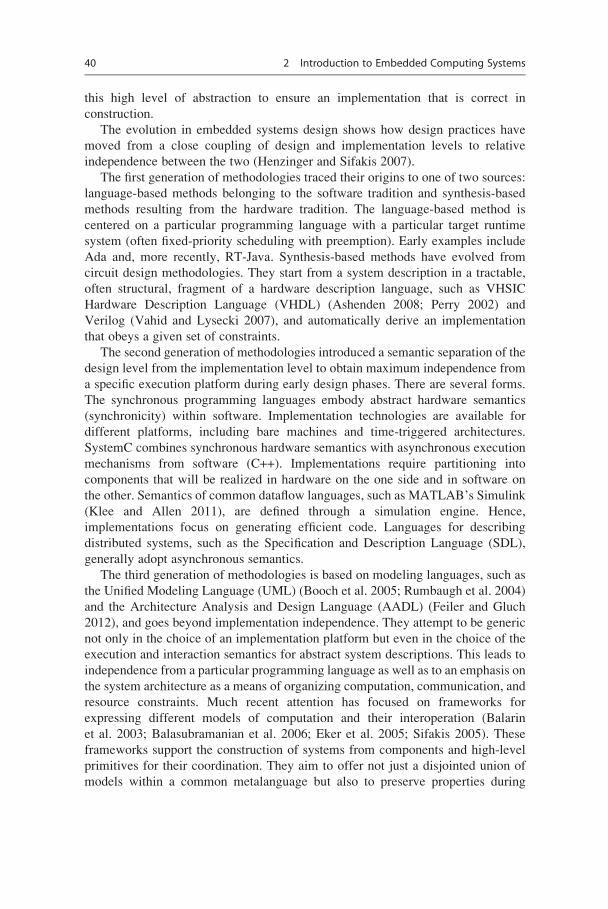
science and engineering (Fig. 2.1).
2.2 Hardware Architectures of Embedded Computing Systems
Embedded computing systems are usually based on standard and application-
specific components, which are based on dedicated hardware constructs in addition
to software, making microprocessors and microcontrollers of particular importance.
Fig. 2.1 PC vs. FPGA-based ECS
2.2 Hardware Architectures of Embedded Computing Systems 41
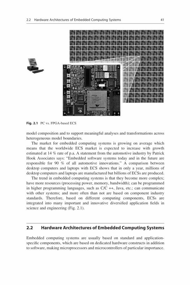
Microprocessors and/or microcontrollers are used to implement the desired system
functionality. For example, the following function can be implemented
total ¼ 0
f or i ¼ 1 toN looptotalþ ¼ M i½ �end loop
on a microprocessor (μP), also called a general-purpose processor (GPP), micro-
controller (μC), digital signal processor (DSP), single-purpose processor (SPP),
application-specific processor (ASP), or programmable logic device (PLD).
The basic architectural concept of the microprocessor (μP/GPP) is shown in
Fig. 2.2. It includes:
• Programmable units that can be used in many applications
• Typical features of the μP/GPP are:
– Program memory
– Generalized dataflow path with a great arithmetic logic register file and unit
(ALU)
• Advantages for the user
– Short time to market
– Low nonrecurring engineering costs (NRE)
– Great flexibility
When compared, the microprocessor differs from the microcontroller in essen-
tial ways. Besides the standard processor core, the microprocessor has more
Fig. 2.2 Basic concept of a microprocessor kernel
42 2 Introduction to Embedded Computing Systems
independently operating units for specific tasks, which are integrated on its chip.
This unit can be, for example, an analog-to-digital converter converting input
analog signals and a digital-to-analog converter converting the processed digital
information into analog output information. The several types of microcontrollers
have different types of special components integrated to adapt to the application
domain of the embedded computing system.
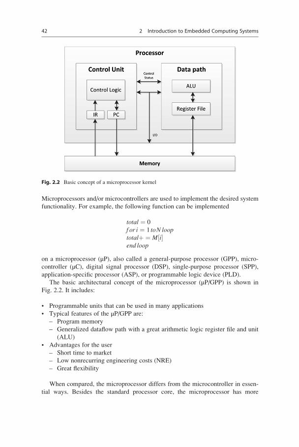
The basic architecture concept of a single-purpose processor (SPP) is shown in
Fig. 2.3. It includes a digital circuit capable of performing a single dedicated
program.
• Technical characteristics:
– Contains only components required to execute a single, dedicated program
– Contains no program memory
• Advantages for the user
– Fast
– Low power consumption
– Small silicon area
The basic architecture concept of an application-specific processor (ASP) is
similar to the one shown in Fig. 2.2. It includes a programmable processor
optimized for a class of particulate applications with the same characteristics.
• Compromise between μP and SPP
• Technical characteristics of the ASP
– Program memory
Fig. 2.3 Basic concept of a single-purpose processor kernel
2.2 Hardware Architectures of Embedded Computing Systems 43
– Optimized dataflow
– Specific functional units
• Advantages for the user
– Flexibility
– Performance
– Low consumption of silicon area
– Saves on power consumption
2.2.1 Programmable Logic Devices
Custom logic devices have been fabricated on the basis of a customer’s
specifications (full customized circuit) for a special logic circuit. To achieve an
acceptable unit price, a higher production quantity is required, which is not usually
the case because of the specific design of the logic circuits. This resulted in the
introduction of semicustom logic blocks (semicustomized circuit). The name comes
from the fact that half-finished, integrated logic blocks of high integration density
were produced in large quantities with final programming by the customer. These
programmable logic devices (PLD) achieved very high growth rates because they
are very flexible and are a less expensive solution due to the large quantities
produced. In addition, the rapid technological progress has resulted in noticeable
advanced technical specifications such as:
• Gate density
• Speed
• Cost
• Architectural flexibility
• Technology
• Housing dimensions
• Development tools
Thus, the gate density increased from an initial 100 to 500 simple-sized circuits
to more than 100,000 usable gates of complex-sized circuits—and has now reached
gate densities of more than one million in complex field programmable gate arrays
(FPGAs)—where the initial signal delays of 45 ns could be reduced to less than
10 ps. The initial set, consisting of a dual in-line package (DIP) with 20 terminals,
was gradually replaced by a pin grid array with 175 or more connections; and
plastic quad flat packs were replaced with 154 or 160 ports and more. Programming
these semicustom logic devices can be accomplished in two different ways:
• Mask programming (manufacturer)
• Field programming (user)
The mask-programming process is part of the entire logic circuit, usually
developed by the user and supplied to the manufacturer for implementation.
44 2 Introduction to Embedded Computing Systems
Leveraging an existing partial design or complete disclosure of the customer’s
circuit design to the manufacturer makes this a sensitive issue if competitors of
the circuit designer have their products manufactured at the same site. Therefore,
designers started to move away from this design technology by introducing field-
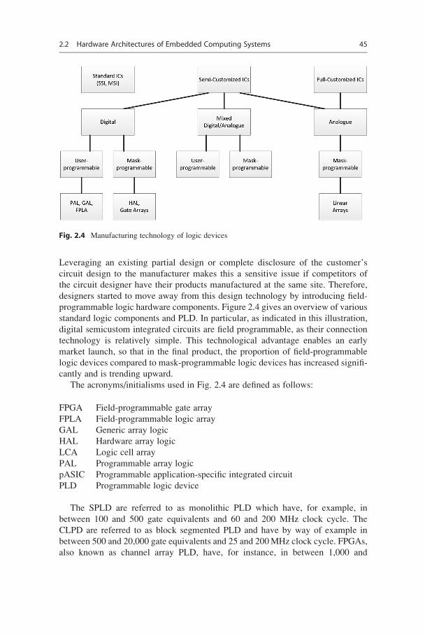
programmable logic hardware components. Figure 2.4 gives an overview of various
standard logic components and PLD. In particular, as indicated in this illustration,
digital semicustom integrated circuits are field programmable, as their connection
technology is relatively simple. This technological advantage enables an early
market launch, so that in the final product, the proportion of field-programmable
logic devices compared to mask-programmable logic devices has increased signifi-
cantly and is trending upward.
The acronyms/initialisms used in Fig. 2.4 are defined as follows:
FPGA Field-programmable gate array
FPLA Field-programmable logic array
GAL Generic array logic
HAL Hardware array logic
LCA Logic cell array
PAL Programmable array logic
pASIC Programmable application-specific integrated circuit
PLD Programmable logic device
The SPLD are referred to as monolithic PLD which have, for example, in
between 100 and 500 gate equivalents and 60 and 200 MHz clock cycle. The
CLPD are referred to as block segmented PLD and have by way of example in
between 500 and 20,000 gate equivalents and 25 and 200MHz clock cycle. FPGAs,
also known as channel array PLD, have, for instance, in between 1,000 and
Fig. 2.4 Manufacturing technology of logic devices
2.2 Hardware Architectures of Embedded Computing Systems 45
1,000,000 gate equivalents and 10 and 100 MHz clock cycle. This classification is
arbitrary and neither complete nor disjointed; it only results from the effort to create
a structural overview.
2.2.2 Field-Programmable Gate Arrays
Field-programmable gate arrays (FPGAs) provide the greatest degree of freedom,
as their chip area is limited either by folding or blocking in their utilization. In
particular, the automated synthesis is advantageously supported by the internal
structure of the FPGA. An FPGA also exhibits consistent and uniform structures,
distinguishing between four classes:
• Symmetric arrays
• Series array
• Sea-of-gates
• Hierarchical PLD
Thus, FPGAs include more than 106 programmable elements on one chip and
must satisfy the following properties for programmable elements:
• Minimum chip area
• Low- and high-resistance OFF
• Low parasitic capacitances, wherein the programming by static random-access
memory (SRAM), erasable programmable read-only memory (EPROM), elec-
trically erasable programmable read-only memory (EEPROM), or antifuse tech-
nology is realized
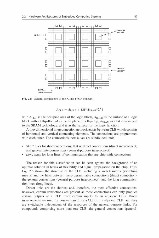
The architecture of the Xilinx FPGA, shown in Fig. 2.5, consists of:
• Configurable logic blocks (CLB)
• Input/output blocks (I/O block)
The CLB are composed of the basic elements, input block, output block, and
logic operation, which are the smallest programmable units in FPGA. Internally,
there are CLB from combinatorial sequential logic elements, so that inputs ia–ie andoutputs QX and QY can be combined with each other twice in any way. The signal
appearing at the outputs can be created from the logic operations in the CLB,
combinatorial or clocked, or represent the latched signal di. Control signals for theCLB are ce (clock enable), k (clock), and rd (asynchronous reset directly). These
signals control the CLB with appropriate internal concession. The number of CLB
in a FPGA depends on the device. The area occupied by a CLB can be estimated as
a function of the technology used, as follows:
46 2 Introduction to Embedded Computing Systems
ACLB ¼ ARLLB þ M*ASRAM*2K
� �with ACLB as the occupied area of the logic block, ARLLB as the surface of a logic
block without flip-flop, M as the bit plane of a flip-flop, ASRAM as a bit area subject
to the SRAM technology, and K as the surface for the logic function.
A two-dimensional interconnection network exists between CLB which consists
of horizontal and vertical connecting elements. The connections are programmed
with each other. The connections themselves are subdivided into:
• Short lines for short connections, that is, direct connections (direct interconnect)and general interconnections (general-purpose interconnect)
• Long lines for long lines of communication that are chip-wide connections
The reason for this classification can be seen against the background of an
optimal solution in terms of flexibility and signal propagation on the chip. Thus,
Fig. 2.6 shows the structure of the CLB, including a switch matrix (switching
matrix) and the links between the programmable connections (direct connection),
the general connections (general-purpose interconnect), and the long communica-
tion lines (long lines).
Direct links are the shortest and, therefore, the most effective connections;
however, certain restrictions are present as these connections can only produce
certain outputs at a CLB from certain inputs to an adjacent CLB. Direct
interconnects are used for connections from a CLB to its adjacent CLB, and they
are switchable independent of the resources of the general-purpose links. For
compounds comprising more than one CLB, the general connections (general-
Fig. 2.5 General architecture of the Xilinx FPGA concept
2.2 Hardware Architectures of Embedded Computing Systems 47
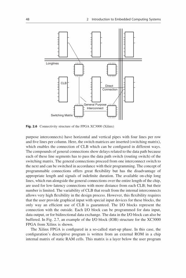
purpose interconnects) have horizontal and vertical pipes with four lines per row
and five lines per column. Here, the switch matrices are inserted (switching matrix),
which enables the connection of CLB which can be configured in different ways.
The compounds of general connections show delays related to the data path because
each of these line segments has to pass the data path switch (routing switch) of the
switching matrix. The general connections proceed from one interconnect switch to
the next and can be switched in accordance with their programming. The concept of
programmable connections offers great flexibility but has the disadvantage of
appropriate length and signals of indefinite duration. The available on-chip long
lines, which run alongside the general connections over the entire length of the chip,
are used for low-latency connections with more distance from each CLB; but their
number is limited. The variability of CLB that result from the internal interconnects
allows very high flexibility in the design process. However, this flexibility requires
that the user provide graphical input with special input devices for these blocks, the
only way an efficient use of CLB is guaranteed. The I/O blocks represent the
connection with the outside. Each I/O block can be programmed for data input,
data output, or for bidirectional data exchange. The data in the I/O block can also be
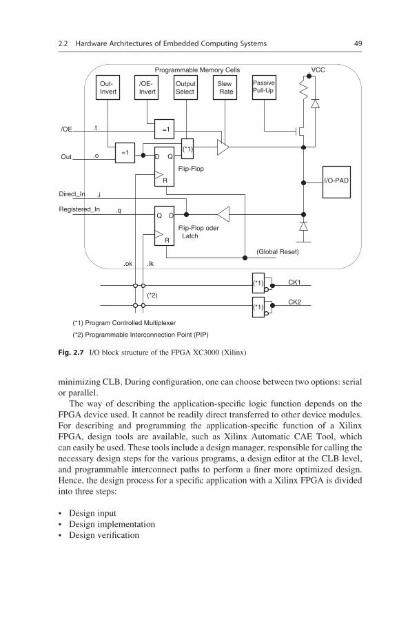
buffered. In Fig. 2.7, an example of the I/O block (IOB) structure for the XC3000
FPGA from Xilinx is shown.
The Xilinx FPGA is configured in a so-called start-up phase. In this case, the
configuration’s descriptive program is written from an external ROM in a chip
internal matrix of static RAM cells. This matrix is a layer below the user program
General PurposeInterconnect
DirectConnection
CLB
Switching Matrix
Longlines
Fig. 2.6 Connectivity structure of the FPGA XC3000 (Xilinx)
48 2 Introduction to Embedded Computing Systems
minimizing CLB. During configuration, one can choose between two options: serial
or parallel.
The way of describing the application-specific logic function depends on the
FPGA device used. It cannot be readily direct transferred to other device modules.
For describing and programming the application-specific function of a Xilinx
FPGA, design tools are available, such as Xilinx Automatic CAE Tool, which
can easily be used. These tools include a design manager, responsible for calling the
necessary design steps for the various programs, a design editor at the CLB level,
and programmable interconnect paths to perform a finer more optimized design.
Hence, the design process for a specific application with a Xilinx FPGA is divided
into three steps:
• Design input
• Design implementation
• Design verification
=1
=1
Out
/OE
Out-Invert
/OE-Invert
D Q
OutputSelect
SlewRate
PassivePull-Up
R
Flip-Flop
DQ
R
Flip-Flop oder
I/O-PAD
Latch
Direct_In
Registered_In
(*1)
(Global Reset)
(*1)
(*1)
CK1
CK2
.o
.i
.q
.t
.ik.ok
Programmable Memory Cells VCC
(*2)
(*1) Program Controlled Multiplexer
(*2) Programmable Interconnection Point (PIP)
Fig. 2.7 I/O block structure of the FPGA XC3000 (Xilinx)
2.2 Hardware Architectures of Embedded Computing Systems 49
The design input is the input of the functional diagram for the application, done
with a specific design editor, with which the logic scheme of the application, based
on basic building blocks (logic functions), macros (counter, register, flip-flop), and
connecting lines, is designed. Thus, the schematic description of the application is
shown in the output file of the design editor which is associated with a specific
interface protocol in the device-specific format, such as Xilinx Netlist File, which
contains all of the necessary information on the blueprint. During the design
implementation, the functional scheme prompted is stepwise implemented to the
specific architecture of the FPGA device. Although the design is first checked for
logical errors, e.g., lack of connections at a gate, thereafter, unnecessary logic
components are removed, which corresponds to minimization of the logic hardware
design. The next step is the transfer of the logical functions of the elements of the
FPGA that are CLB and IOB. For this purpose, the function of the design is
partitioned to the individual blocks. If the logic function can be partitioned to the
existing blocks on the chip, then the necessary compounds are selected (routing)
and inserted into the resulting design file. From this file, a specific place-and-route
algorithm is generated as well as the corresponding configuration program for the
FPGA. The design verification involves simulating the functionality and the tem-
poral behavior during the scheme entry. Compared to the large CLB Xilinx FPGA
architectures, the Actel FPGA consists of rows of small, simple logic modules and
IOB. A two-dimensional connection network exists between the programmable
logic modules, consisting of horizontal and vertical connections. The connection
resources are split into:
• Input segments
• Output segments
• Clock lines
• Connecting segments
A connecting segment is comprised of four input segments connected via logic
modules. The output segment connects the output of a logic module with
connecting channels above and below the block. The clock lines are special
low-delay connections for connecting several logic modules. The connection
segments consist of metallic conductors of different lengths, which can be assem-
bled using antifuse technology to create longer lines. In contrast to the previously
discussed Actel FPGA concept, the Crosspoint FPGAs belong to the class of serial
block structure FPGA architectures similar to the class of hierarchical Altera PLD.
Field-programmable gate arrays satisfying the hierarchical PLD architecture are
also available from Advanced Micro Devices (AMD). The architecture is based on
the hierarchical grouping of programmable logic array blocks (LAB) in EPROM
technology and consists of two types of cells:
• Programmable LAB
• IOB
50 2 Introduction to Embedded Computing Systems
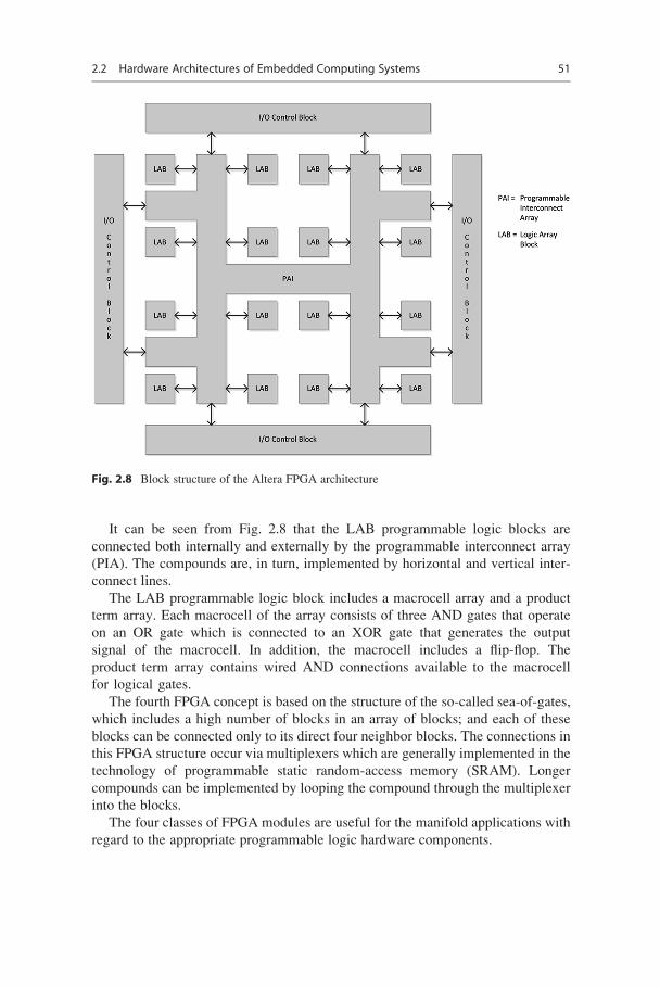
It can be seen from Fig. 2.8 that the LAB programmable logic blocks are
connected both internally and externally by the programmable interconnect array
(PIA). The compounds are, in turn, implemented by horizontal and vertical inter-
connect lines.
The LAB programmable logic block includes a macrocell array and a product
term array. Each macrocell of the array consists of three AND gates that operate
on an OR gate which is connected to an XOR gate that generates the output
signal of the macrocell. In addition, the macrocell includes a flip-flop. The
product term array contains wired AND connections available to the macrocell
for logical gates.
The fourth FPGA concept is based on the structure of the so-called sea-of-gates,
which includes a high number of blocks in an array of blocks; and each of these
blocks can be connected only to its direct four neighbor blocks. The connections in
this FPGA structure occur via multiplexers which are generally implemented in the
technology of programmable static random-access memory (SRAM). Longer
compounds can be implemented by looping the compound through the multiplexer
into the blocks.
The four classes of FPGA modules are useful for the manifold applications with
regard to the appropriate programmable logic hardware components.
Fig. 2.8 Block structure of the Altera FPGA architecture
2.2 Hardware Architectures of Embedded Computing Systems 51
2.3 Design Metrics
Both market requirements and technological developments have had a huge influ-
ence in the design of ECS in recent years. The situation is characterized by the fact
that the complexity of ECS constantly increases. This is, on the one hand, marked
by the technical innovation cycles of development; and, on the other hand, it is
marked by the increase in product requirements. Complexity arises based not only
on the number of merged single components in the ECS but also on the heteroge-
neity of used hardware and software partitions that only allow, as a whole, the
required functionality. This requires a methodology for designing complex
structures with appropriate interfaces between the different components including
their integration into the system environment while considering the continuous
improvement of implementation technology. The design of ECS becomes more
challenging due to increasing system complexity as well as relentless time-to-
market pressure. Hence, a measurable feature of the system implementation is
required to map the relationships and the performance level of the systems design
demonstrating to what extent the present design meets system specification quality
standards, such as IEEE Standard 1061, 1992. This can be expressed by means of a
membership function, which maps the requirements with regard to a target func-
tion. The mathematical representation of the features of the design must satisfy the
specifications determined by a metric. With metrics one can:
• Compare drafts of embedded computing systems designs with regard to the
fulfillment of their specifications, i.e., a formal comparison and assessment
option
• Deal with the increased system complexity and/or requirements in embedded
computing systems
• Compare the development and test costs with regard to constraints of the
hardware-software partitioning of the embedded computing system to identify
the optimal match in the functionality breakdown among the hardware and
software components
• Identify the risk of time-to-market constraints assumed in the development and
production of embedded computing systems
Against this background, the manufacturer always has to comply with shorter
product development in order to launch product innovations into the market more
quickly. This requires product development and manufacturing focused on time to
market, as the economic success of a product depends on its timely availability.
This results in:
• Time pressure in the development and production of embedded computing
systems and their optimal service and/or maintenance
• Reusing hardware and software components
• Continuity and penetrability in the design of embedded computing systems
52 2 Introduction to Embedded Computing Systems
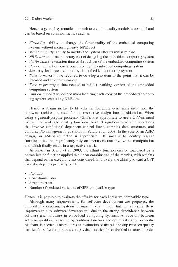
Hence, a general systematic approach to creating quality models is essential and
can be based on common metrics such as:
• Flexibility: ability to change the functionality of the embedded computing
system without incurring heavy NRE cost
• Maintainability: ability to modify the system after its initial release
• NRE cost: one-time monetary cost of designing the embedded computing system
• Performance: execution time or throughput of the embedded computing system
• Power: amount of power consumed by the embedded computing system
• Size: physical space required by the embedded computing system
• Time to market: time required to develop a system to the point that it can be
released and sold to customers
• Time to prototype: time needed to build a working version of the embedded
computing system
• Unit cost: monetary cost of manufacturing each copy of the embedded comput-
ing system, excluding NRE cost
Hence, a design metric to fit with the foregoing constraints must take the
hardware architecture used for the respective design into consideration. When
using a general-purpose processor (GPP), it is appropriate to use a GPP-oriented
metric. The goal is to identify functionalities that significantly rely on operations
that involve conditional dependent control flows, complex data structures, and
complex I/O management, as shown in Sciuto et al. 2003. In the case of an ASIC
design, an ASIC-like metric is appropriate. The goal is to identify regular
functionalities that significantly rely on operations that involve bit manipulation
and which finally result in a respective metric.
As shown in Sciuto et al. 2003, the affinity function can be expressed by a
normalization function applied to a linear combination of the metrics, with weights
that depend on the executor class considered. Intuitively, the affinity toward a GPP
executor depends primarily on the
• I/O ratio
• Conditional ratio
• Structure ratio
• Number of declared variables of GPP-compatible type
Hence, it is possible to evaluate the affinity for each hardware-compatible type.
Although many improvements for software development are proposed, the
embedded computing systems designer faces a hard task in applying these
improvements to software development, due to the strong dependence between
software and hardware in embedded computing systems. A trade-off between
software qualities, measured by traditional metrics and optimization for a specific
platform, is needed. This requires an evaluation of the relationship between quality
metrics for software products and physical metrics for embedded systems in order
2.3 Design Metrics 53
to guide a designer in selecting the best design alternative during design space
exploration at the model level (Oliveira et al. 2008).
A metric which describes the general procedure for creating a quality model
includes:
• Describe the environment of the company and the project as well as the task, and
define the reviews
• Define the goals
• Define assessment objectives and associated metrics
• Define a workflow for data collection
• Collect, analyze, and interpret data
• Summarize and apply the experience to develop best practices
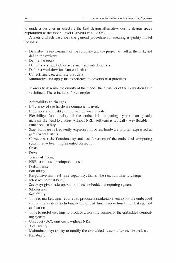
In order to describe the quality of the model, the elements of the evaluation have
to be defined. These include, for example:
• Adaptability to changes.
• Efficiency of the hardware components used.
• Efficiency and quality of the written source code.
• Flexibility: functionality of the embedded computing system can greatly
increase the need to change without NRE; software is typically very flexible.
• Functional safety
• Size: software is frequently expressed in bytes; hardware is often expressed as
gates or transistors
• Correctness: the functionality and test functions of the embedded computing
system have been implemented correctly
• Costs
• Power
• Terms of storage
• NRE: one-time development costs
• Performance
• Portability
• Responsiveness: real-time capability, that is, the reaction time to change
• Interface compatibility
• Security: given safe operation of the embedded computing system
• Silicon area
• Scalability
• Time to market: time required to produce a marketable version of the embedded
computing system including development time, production time, testing, and
evaluation
• Time to prototype: time to produce a working version of the embedded comput-
ing system
• Unit cost (UC): unit costs without NRE
• Availability
• Maintainability: ability to modify the embedded system after the first release
• Reliability
54 2 Introduction to Embedded Computing Systems
Therefore, the goal node metric enables the assessment on the basis of the
specified range of elements. These can question, for example, the development
process of ECS with a goal of functional safety with respect to the efficiency of the
source code, from the perspective of the customer and in the context of the NRE
which can be described as follows:
Assessment element Metric Description
1 1.1 Adaptation to known process
1.2 New process
2 2 High requirement
3 3.1 Structogram
3.2 XML
4 4 High
5 5.1 Low
5.2 Moderate
For the above example, the degree to which membership functions are given can
be expressed in the form of an n-tuple notation:
minE Ψð Þ ¼ E ΨM1:1, ΨM1:2, ΨM2, ΨM3:1, ΨM3:2, ΨM4, ΨM5:1, ΨM5:2ð Þwhere M1.x¼ process functional, M2¼ requirements functional, M3.x¼ func-
tional code, M4¼ customer functional, and M5.x¼ project requirements func-
tional, whereby
Ψ M1:x, M2, M3:x, M4, M5:xð Þ ¼ 0 f orM1:x ¼ M2 ¼ M3:x ¼ M4 ¼ M5:xΨ M1:x, M2, M3:x, M4, M5:xð Þ ¼ 1 f orM1:x 6¼ M2 6¼ M3:x 6¼ M4 6¼ M5:x
with
M1:x, M2, M3:x, M4, M5:x2Πwhere Ψ is a metric of Π. Thus, the degree of fulfillment of the membership
function can be exemplified as follows:
minE Ψð Þ ¼ E 1, 0, 1, 0, 1, 1, 1, 0ð Þthat is, the development process of the ECS has been optimally adapted to the
known simple process; a new process must not be created; the high requirement for
functional safety is optimally fulfilled; requirements on the efficiency and the
quality of the written source code are optimally fulfilled; the design of the ECS
optimally fit from the perspective of the customer; and the NRE has been optimally
fulfilled due to the low requirements on the project. In addition to the specified
values 0 and 1 for the degree of fulfillment of the membership function, intermedi-
ate values are possible, such as 0.1, 0.2, 0.3, . . ., 0.9, and 1.0.
2.3 Design Metrics 55
2.4 Embedded Control Systems
The concept of control systems represents a very common class of embedded
systems. The concept describes a process in which the control system seeks to
make a system’s output, whose dynamic depends on the chosen system’s plant
model, track a desired input without feedback from the system’s output, which is
called open-loop control. Thus, the design of an embedded control system improves
systems performance with regard to:
• System accuracy
• Speed of system response, allowable overshoot, and maximum duration of
settling time
• Stability
A closed-loop control system provides feedback from the system’s output to the
reference input for further processing. Effects of disturbances can be detected and
compensated for by appropriate control actions, which are characterized both in
terms of strength and in terms of time sequences. This compensation is based on
feedback with a negative sign. Therefore, the following relationships can be
derived:
• Control process is triggered by disturbances acting on the plant of the embedded
closed-loop control system.
• Disturbance occurs and is identified in an embedded closed-loop control system
which continuously observes and compares the system’s output with the refer-
ence input.
• A deviation of the actual system output from the reference input in a closed-loop
embedded control system releases an adaptation to the set value. Therefore, the
impact of disturbances is clearly eased. To achieve this effect, a reversal sign has
to be introduced in the closed-loop action.
• The closed action of an embedded control operation is self-contained. Hence, the
temporal sequence of reactions of the control loop is determined by the used
parts described by their transfer functions. They follow the principle of causality,
that is, the control circuit generates the cause toward the associated response
(effect). For this purpose, passing through the control loop, the input excitation
of a block element’s transfer function is transferred to the output according to the
transfer function of the controlled system. The information shall always be
directed, i.e., in one direction. Hence, directed arrows (called action lines) are
identified in the representation of a control system.
2.4.1 Control
The control refers to the directed influence of a process whose properties corre-
spond to the observed block transfer elements. Activities in the control system
56 2 Introduction to Embedded Computing Systems
which influence one or more variables as input variables and other variables as
output variables are based on the system’s intrinsic laws. Moreover, in control
systems, the system’s output not only depends on the unilateral impact of the
arrangement of the reference input (set value) but also depends on the disturbances
occurring. The reference input acts as a control input for the output block transfer
element according to physical laws and links and/or timing so that the desired
behavior is established. Although, the system’s output has no influence on the
reference input (missing feedback), the system’s output may differ due to external
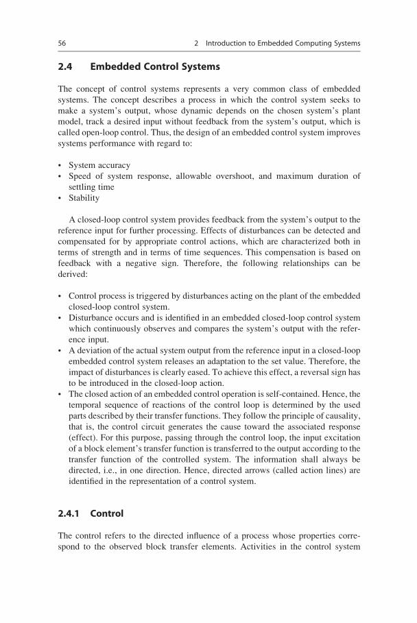
disturbances from the desired target value. Hence, an embedded control system can
be introduced as an open-loop-block-based transfer function consisting of a number
of transfer block components connected in series. The control principle in its
conceptual annotation is shown in Fig. 2.9.
In real control systems, disturbances frequently occur at any time and in any
amplitude through which their influence on the system’s output may be signifi-
cantly displaced from the reference input. Against this background, it is useful to
capture the system’s output by a separate transfer block. In case of deviations of the
system’s output from the reference input, the influence of the disturbance on the
plant can be compensated for through the principle of feedback control. Thus, with
a simple open-loop control system, one cannot act against foreseeable disturbance.
Hence, a system is required which in the simplest case has transfer components for
observing the system’s output and comparing it with the reference input to calculate
the error between them, forcing the system’s output to follow the reference input.
This principle is the closed-loop control system.
2.4.2 Feedback Control
The concept of feedback describes a control system in which the system’s output,
whose dynamic depends on the chosen system’s plant model, is forced to follow a
reference input while remaining relatively insensitive to the effects of disturbances.
In the case of a difference between both signals, the summing point of the feedback
loop generates an error signal which is transferred to the controller input. The
controller acts on the error with regard to a control strategy and manipulates the
plant model to make it track the reference input. Moreover, this closed-loop
feedback forces the system’s output to follow the reference input with regard to
present disturbance inputs. Thus, closed-loop control contains more transfer
elements than open-loop control. The transfer elements of a closed-loop control are:
Fig. 2.9 Block diagram structure of a control system
2.4 Embedded Control Systems 57
• Plant or process: system to be controlled.
• System output: particular system aspect to be controlled.
• Reference input: quantity desired for the system’s output.
• Actuator: device used to control input to the plant or process.
• Controller: device used to generate input to the actuator or plant to force the
system’s output to follow the reference input. Therefore, the controller contains
the control strategy to make the desired output track the desired reference input.
• Disturbance: additional undesirable input to the plant imposed by the environ-
ment that may cause the system’s output to differ from the expected output with
regard to the reference input.
To this point, these transfer elements are the same in an open-loop control
system. The closed-loop control system has the following additional transfer
elements:
• Sensor: device to measure system output
• Error detector: determines the difference between the measured system output
and reference input
Therefore, a closed-loop controller continuously detects and compares the
potential difference between the reference input and the system’s output by making
use of the sensor and error detector. The resulting error value of the error detector is
read by the controller’s input which then computes a setting for the actuator to
manipulate the actuator and, thereafter, the plant of the closed-loop embedded
control system. The controller uses the feedback from the error detector to force
the system’s output based on the control law of the controller which has been
implemented. The actuator modifies the input to the plant with regard to the
requirements based on the error detector output and the controller transfer function.
In Fig. 2.10, the block diagram of a closed-loop control system is shown, with its
conceptual annotation, referring to the transfer elements described above.
The terms occurring from the closed action sequence in the control loop cycle
are summarized in the following table:
Symbol Denomination
u(t) Reference input or set value
xd(t) Error detection or control deviation
y(t) Control output or correcting input
r(t) Actuatingoutput
z(t) Disturbance input
x(t) System output or control variable
xR(t) Measured system output or measured control variable
In Fig. 2.10, the structure of control systems is presented in block diagram form,
depicted as an interconnection of symbols representing certain basic mathematical
operations in such a way that the overall diagram obeys the system’s mathematical
58 2 Introduction to Embedded Computing Systems
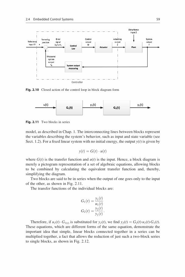
model, as described in Chap. 1. The interconnecting lines between blocks represent
the variables describing the system’s behavior, such as input and state variable (see
Sect. 1.2). For a fixed linear system with no initial energy, the output y(t) is given by
y tð Þ ¼ G tð Þ � u tð Þwhere G(t) is the transfer function and u(t) is the input. Hence, a block diagram is
merely a pictogram representation of a set of algebraic equations, allowing blocks
to be combined by calculating the equivalent transfer function and, thereby,
simplifying the diagram.
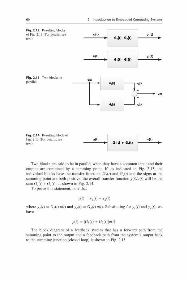
Two blocks are said to be in series when the output of one goes only to the input
of the other, as shown in Fig. 2.11.
The transfer functions of the individual blocks are:
G1 tð Þ ¼ y1 tð Þu1 tð Þ
G2 tð Þ ¼ y2 tð Þy1 tð Þ :
Therefore, if u1(t) ·G1(t) is substituted for y1(t), we find y2(t) ¼ G2(t)·u1(t)·G1(t).These equations, which are different forms of the same equation, demonstrate the
important idea that simple, linear blocks connected together in a series can be
multiplied together, a fact that allows the reduction of just such a two-block series
to single blocks, as shown in Fig. 2.12.
Fig. 2.10 Closed action of the control loop in block diagram form
Fig. 2.11 Two blocks in series
2.4 Embedded Control Systems 59
Two blocks are said to be in parallel when they have a common input and their
outputs are combined by a summing point. If, as indicated in Fig. 2.13, the
individual blocks have the transfer functions G1(t) and G2(t) and the signs at the
summing point are both positive, the overall transfer function y(t)/u(t) will be the
sum G1(t) + G2(t), as shown in Fig. 2.14.
To prove this statement, note that
y tð Þ ¼ y1 tð Þ þ y2 tð Þwhere y1(t) ¼ G1(t)·u(t) and y2(t) ¼ G2(t)·u(t). Substituting for y1(t) and y2(t), wehave
y tð Þ ¼ G1 tð Þ þ G2 tð Þ½ �u tð Þ:The block diagram of a feedback system that has a forward path from the
summing point to the output and a feedback path from the system’s output back
to the summing junction (closed loop) is shown in Fig. 2.15.
Fig. 2.12 Resulting blocks
of Fig. 2.11 (For details, see
text)
Fig. 2.13 Two blocks in
parallel
Fig. 2.14 Resulting block of
Fig. 2.13 (For details, see
text)
60 2 Introduction to Embedded Computing Systems
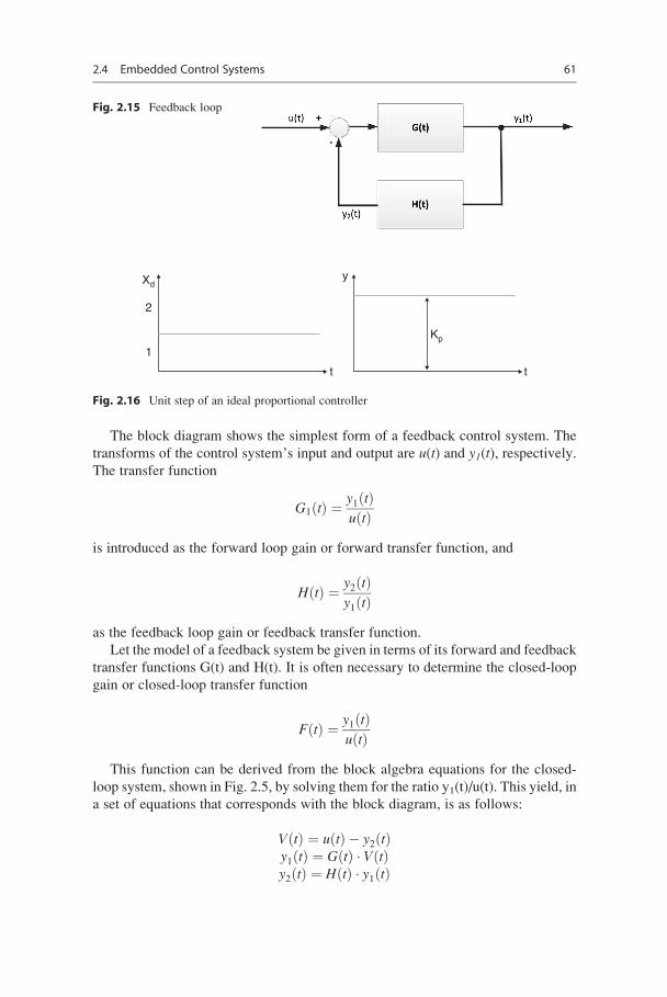
The block diagram shows the simplest form of a feedback control system. The
transforms of the control system’s input and output are u(t) and y1(t), respectively.The transfer function
G1 tð Þ ¼ y1 tð Þu tð Þ
is introduced as the forward loop gain or forward transfer function, and
H tð Þ ¼ y2 tð Þy1 tð Þ
as the feedback loop gain or feedback transfer function.
Let the model of a feedback system be given in terms of its forward and feedback
transfer functions G(t) and H(t). It is often necessary to determine the closed-loop
gain or closed-loop transfer function
F tð Þ ¼ y1 tð Þu tð Þ
This function can be derived from the block algebra equations for the closed-
loop system, shown in Fig. 2.5, by solving them for the ratio y1(t)/u(t). This yield, in
a set of equations that corresponds with the block diagram, is as follows:
V tð Þ ¼ u tð Þ � y2 tð Þy1 tð Þ ¼ G tð Þ � V tð Þy2 tð Þ ¼ H tð Þ � y1 tð Þ
Fig. 2.15 Feedback loop
2
Xd
Kp
1
t
y
t
Fig. 2.16 Unit step of an ideal proportional controller
2.4 Embedded Control Systems 61
Let us combine these equations to eliminate V(t) and y2(t) yields
y1 tð Þ ¼ G tð Þ � u tð Þ � H tð Þ � y1 tð Þ½ �which can be rearranged to give
1þ G tð Þ � H tð Þ½ �y1 tð Þ ¼ G tð Þ � u tð ÞHence, the closed-loop gain or closed-loop transfer function
F tð Þ ¼ y1 tð Þu tð Þ
is
F tð Þ ¼ G tð Þ1þ G tð Þ � H tð Þ :
It is clear that the sign of the feedback signal at the summing point is negative.
Assuming that the sign at the summing point is positive for the feedback signal,
then the closed-loop gain or closed-loop transfer function will become negative.
Assuming a commonly used simplification occurs when the feedback transfer
function is unity, which means that H(t)¼ 1, this control system is called a unity
feedback system, yielding:
F tð Þ ¼ G tð Þ1� G tð Þ :
2.4.3 Feedback Components of Embedded Control Systems
In practice, specific feedback transfer functions are used when designing embedded
control systems. These closed-loop transfer function characteristics can be
described by the:
• Transient behavior or static characteristic curves
• Mathematical methods
The mathematical notation of the respective feedback law for the dynamic
behavior of embedded closed-loop control system transfer functions depends on
the chosen characteristic of the specific controller block. In practice, the following
elements are of importance:
• Proportional control
• Integral control
• Derivative control
62 2 Introduction to Embedded Computing Systems
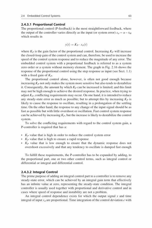
2.4.3.1 Proportional ControlThe proportional control (P-feedback) is the most straightforward feedback, where
the output of the controller varies directly as the input (or system error) xd ¼ u – xRwhich results in
y tð Þ ¼ KP � xd tð Þwhere KP is the gain factor of the proportional control. Increasing KP will increase
the closed-loop gain of the control system and can, therefore, be used to increase the
speed of the control system response and to reduce the magnitude of any error. The
embedded control system with a proportional feedback is referred to as a system
zero order or a system without memory element. The graph in Fig. 2.16 shows the
response of the proportional control using the step response as input (see Sect. 1.1)
with a fixed gain of KP.
The proportional control alone, however, is often not good enough because
increasing KP not only makes the system more sensitive but also tends to destabilize
it. Consequently, the amount by which KP can be increased is limited; and this limit
may not be high enough to achieve the desired response. In practice, when trying to
adjust KP, conflicting requirements may occur. On one hand, it is intended to reduce
any steady-state error as much as possible; but to attempt this by increasing KP is
likely to cause the response to oscillate, resulting in a prolongation of the settling
time. On the other hand, the response to any change of the input signal should be as
fast as possible but with little overshoot or oscillation. Fast control system response
can be achieved by increasing KP, but the increase is likely to destabilize the control
system.
To solve the conflicting requirements with regard to the control system gain, a
P-controller is required that has a:
• KP value that is high in order to reduce the control system error
• KP value that is high to ensure a rapid response
• KP value that is low enough to ensure that the dynamic response does not
overshoot excessively and that any tendency to oscillate is damped fast enough
To fulfill these requirements, the P-controller has to be expanded by adding, to
the proportional part, one or two other control terms, such as integral control or
differential or integral and differential control.
2.4.3.2 Integral ControlThe prime purpose of adding an integral control part to a controller is to remove any
steady-state error, which can be achieved by an integral gain term that effectively
has an infinite value at zero, representing the steady-state condition. The integral
controller is usually used together with proportional and derivative control and in
cases where speed of response and instability are not a problem.
An integral control dependence exists for which the output signal x and time
integral of input xd are proportional. Time integration of the control deviation ewith
2.4 Embedded Control Systems 63
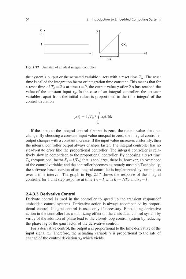
the system’s output or the actuated variable y acts with a reset time TN. The reset
time is called the integration factor or integration time constant. This means that for
a reset time of TN¼ 2 s at time t¼ 0, the output value y after 2 s has reached the
value of the constant input xd. In the case of an integral controller, the actuator
variabler, apart from the initial value, is proportional to the time integral of the
control deviation
y tð Þ ¼ 1=TN*
Zt1t0
xd tð Þdt
If the input to the integral control element is zero, the output value does not
change. By choosing a constant input value unequal to zero, the integral controller
output changes with a constant increase. If the input value increases uniformly, then
the integral controller output always changes faster. The integral controller has no
steady-state error like the proportional controller. The integral controller is rela-
tively slow in comparison to the proportional controller. By choosing a reset time
TN (proportional factor KI¼ 1/TN) that is too large, there is, however, an overshoot
of the control variable; and the controller becomes extremely unstable Technically,
the software-based version of an integral controller is implemented by summation
over a time interval. The graph in Fig. 2.17 shows the response of the integral
controllerfor a unit step response at time TN¼ 1 with KI¼ 1/TN and xd¼ 1.
2.4.3.3 Derivative ControlDerivate control is used in the controller to speed up the transient responseof
embedded control systems. Derivative action is always accompanied by propor-
tional control. Integral control is used only if necessary. Embedding derivative
action in the controller has a stabilizing effect on the embedded control system by
virtue of the addition of phase lead to the closed-loop control system by reducing
the phase lag of the gain factor of the derivative control.
For a derivative control, the output u is proportional to the time derivative of the
input signal xd. Therefore, the actuating variable y is proportional to the rate of
change of the control deviation xd which yields
t
y
1
2
2s
t
KIXd
Xd
Fig. 2.17 Unit step of an ideal integral controller
64 2 Introduction to Embedded Computing Systems
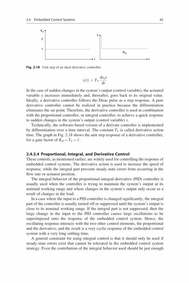
y tð Þ ¼ TVdxdt
dt
.In the case of sudden changes in the system’s output (control variable), the actuated
variable y increases immediately and, thereafter, goes back to its original value.
Ideally, a derivative controller follows the Dirac pulse as a step response. A pure
derivative controller cannot be realized in practice because the differentiation
eliminates the set point. Therefore, the derivative controller is used in combination
with the proportional controller, or integral controller, to achieve a quick response
to sudden changes in the system’s output (control variable) x.Technically, the software-based version of a derivate controller is implemented
by differentiation over a time interval. The constant TV is called derivative action
time. The graph in Fig. 2.18 shows the unit step response of a derivative controller,
for a gain factor of KD¼ TV¼ 1.
2.4.3.4 Proportional, Integral, and Derivative ControlThese controls, as mentioned earlier, are widely used for controlling the response of
embedded control systems. The derivative action is used to increase the speed of
response, while the integral part prevents steady-state errors from occurring in the
flow rate or actuator position.
The integral behavior of the proportional-integral-derivative (PID) controller is
usually used when the controller is trying to maintain the system’s output at its
nominal working range and where changes in the system’s output only occur as a
result of changes in the load.
In a case where the input to a PID controller is changed significantly, the integral
part of the controller is usually turned off or suppressed until the system’s output is
close to its nominal working range. If the integral part is not suppressed, then the
large change in the input to the PID controller causes large oscillations to be
superimposed onto the response of the embedded control system. Hence, the
oscillating response interacts with the two other control elements, the proportional
and the derivative; and the result is a very cyclic response of the embedded control
system with a very long settling time.
A general constraint for using integral control is that it should only be used if
steady-state errors exist that cannot be tolerated in the embedded control system
strategy. Even the contribution of the integral behavior used should be just enough
t t
1
2y
Xd
KD
Fig. 2.18 Unit step of an ideal derivative controller
2.4 Embedded Control Systems 65
to remove the steady-state error without causing the steady response to oscillate.
Where steady-state errors either do not exist or can be tolerated, then a propor-
tional-derivative controller will be sufficient enough.
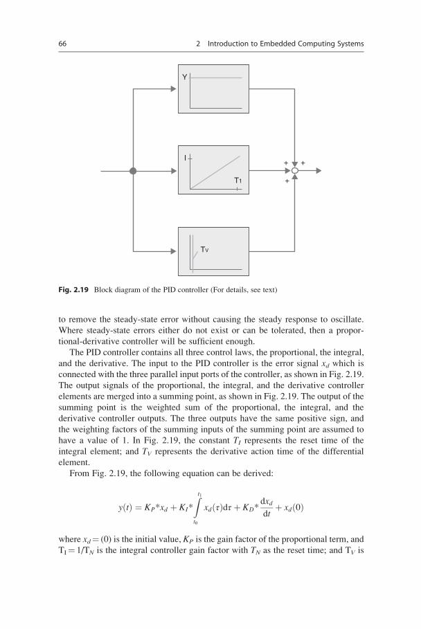
The PID controller contains all three control laws, the proportional, the integral,
and the derivative. The input to the PID controller is the error signal xd which is
connected with the three parallel input ports of the controller, as shown in Fig. 2.19.
The output signals of the proportional, the integral, and the derivative controller
elements are merged into a summing point, as shown in Fig. 2.19. The output of the
summing point is the weighted sum of the proportional, the integral, and the
derivative controller outputs. The three outputs have the same positive sign, and
the weighting factors of the summing inputs of the summing point are assumed to
have a value of 1. In Fig. 2.19, the constant TI represents the reset time of the
integral element; and TV represents the derivative action time of the differential
element.
From Fig. 2.19, the following equation can be derived:
y tð Þ ¼ KP*xd þ KI*
Zt1t0
xd τð Þdτ þ KD*dxddt
þ xd 0ð Þ
where xd¼ (0) is the initial value, KP is the gain factor of the proportional term, and
TI¼ 1/TN is the integral controller gain factor with TN as the reset time; and TV is
Y
I+ +
+T1
TV
Fig. 2.19 Block diagram of the PID controller (For details, see text)
66 2 Introduction to Embedded Computing Systems
the derivative controller gain factor. After excluding KP and with regard to the
boundary condition xd(0)¼ (0), it follows
y tð Þ ¼ KP xd þ TI
KP*
Zt1t0
xd τð Þdτ þ KD
KP*dxddt
0@
1A:
With
KP
TI¼ TN
and
KD
KP¼ TV
we receive:
y tð Þ ¼ KP xd þ 1
TN*
Zt1t0
xd τð Þdτ þ TV*dxddt
0@
1A:
Using the Laplace transform, the above equation can be written as follows with
s as the Laplace operator
G sð Þ ¼ KP 1þ 1
s*TNþ s*TV
� �:
For a number of calculations, it may be more appropriate to rewrite the above
additive form into the following multiplicative form
G sð Þ ¼ KP*1þ sþ T1ð Þ* 1þ s*T2ð Þ
sþ TN:
Comparison of coefficients yields
T1 ¼ TN
21þ
ffiffiffiffiffiffiffiffiffiffiffiffiffiffiffiffi1� 4TV
TN
r� �
T2 ¼ TN
21�
ffiffiffiffiffiffiffiffiffiffiffiffiffiffiffiffi1� 4TV
TN
r� �
where TN> 4*TV. From TN> 5*TV, the following relations can be found
T1 ¼ TN
T2 ¼ TV :
2.4 Embedded Control Systems 67

It can be seen from the above equations that the PID controller has two zero
elements and a pole at the origin of the s-plane. The gain factors, KP, TN, and TV, ofthe PID controller can be calculated using the tangent at the inflection point of the
step response with the abscissa as the lower auxiliary variable TU and the intersec-
tion of the tangent with the 5τ value of the step response as the top auxiliary
variable Tg, as shown in Fig. 2.20.
From Fig. 2.20, the corresponding values for TU and Tg, pictured on the abscissatime t, can be read. Let the PID controller overshoot the quotient of the auxiliary
variableOmax, for the maximum overshoot height at T95 describes the default valuesfor the PID controller
KP ¼ T95
€Umax
*Tg
TU
.Assuming that the PID controller is not allowed to overshoot results in the following
equation with regard to the above-introduced auxiliary variables
KP ¼ T60
KS∗Tg
TUTN ¼ Tg
2 � TV ¼ TU
The ideal PID controller was introduced as a parallel connection of an ideal
proportional-integral-derivative controller, which is represented by the addition of
individual transfer functions as follows
g tð Þ ¼ KP þ KP
TN∗tþ KP∗Tv∗δ tð Þ:
The transfer function g(t) of the ideal PID controller given above can be
illustrated as shown in Fig. 2.21.
Fig. 2.20 Transient behavior
of a step response (For details,
see text)
68 2 Introduction to Embedded Computing Systems
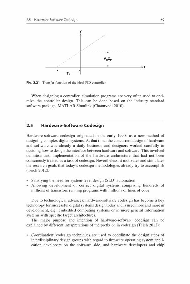
When designing a controller, simulation programs are very often used to opti-
mize the controller design. This can be done based on the industry standard
software package, MATLAB Simulink (Chaturvedi 2010).
2.5 Hardware-Software Codesign
Hardware-software codesign originated in the early 1990s as a new method of
designing complex digital systems. At that time, the concurrent design of hardware
and software was already a daily business; and designers worked carefully in
deciding how to design the interface between hardware and software. This involved
definition and implementation of the hardware architecture that had not been
consciously treated as a task of codesign. Nevertheless, it motivates and stimulates
the research goals that today’s codesign methodologies already try to accomplish
(Teich 2012):
• Satisfying the need for system-level design (SLD) automation
• Allowing development of correct digital systems comprising hundreds of
millions of transistors running programs with millions of lines of code
Due to technological advances, hardware-software codesign has become a key
technology for successful digital systems design today and is used more and more in
development, e.g., embedded computing systems or in more general information
systems with specific target architectures.
The major purpose and intention of hardware-software codesign can be
explained by different interpretations of the prefix co in codesign (Teich 2012):
• Coordination: codesign techniques are used to coordinate the design steps of
interdisciplinary design groups with regard to firmware operating system appli-
cation developers on the software side, and hardware developers and chip
TP
VRXP
t
y
Fig. 2.21 Transfer function of the ideal PID controller
2.5 Hardware-Software Codesign 69
designers on the hardware side, to work together on all parts of a system. This is
also the original interpretation of the Latin syllable co in the word codesign.
• Concurrency: tight time-to-market windows force hardware and software
developers to work concurrently instead of starting the firmware and software
development, as well as their testing, only after the hardware architecture is
available. Codesign has provided enormous progress in avoiding this bottleneck
by either starting from an executable specification and/or applying the concept of
virtual platforms and virtual prototyping to run the concurrently developed
software on a simulation model of the architecture at a very early stage. Also,
testing and partitioning of concurrently executing software and hardware
components require special cosimulation techniques to reflect concurrency and
synchronization of subsystems.
• Correctness: correctness challenges of complex hardware and software
techniques require not only verification of the correctness of each individual
subsystem but also coverification of their correct interactions after their
integration.
• Complexity: codesign techniques are mainly driven by the complexity of today’s
digital systems designs and serve as a means to close the well-known design gap
and produce correctly working, highly optimized (e.g., with respect to cost,
power, or performance) system implementations.
Moreover, the methodology of hardware-software codesign can be explained by
additional interpretations of the syllable co:
• Cosynthesis: marks the fields where hardware or software could be used based
on the possible minimization of communication between application areas
• Cosimulation: permits early review of the system’s logic functionality and
behavior based on partitioning review
• Cotest: set by the user since neither the hardware test methods nor the software
metrics contain application-specific testing methods
The potential results from the co-methods are:
• Abstract system level in the design phase
• Very complex system and high-performance standards
• Short time to market in design and production
• Systems with standard microprocessormicrocontroller components, PCs,
one-chip solutions, DSP, and more
• Systems with application-specific hardware, such as ASIC, ASP; DSP, FPGA,
and more
• Systems with specific software
• Many comprehensive applications
This requires that the available techniques support the complexity management
in hardware and software codesign by:
70 2 Introduction to Embedded Computing Systems
• Hardware-software partitioning
– Decisions are postponed that place constraints on the design when possible.
• Abstractions and decomposition techniques
• Incremental development
– Growing software requires top-down design
• Description languages
• Simulation
• Standards
• Design methodology management framework
The current hardware-software codesign process includes:
• Basic features of the design process
– System immediately partitioned to hardware and software components
– Hardware and software developed separately
– Hardware as first approach is often adopted
• Implications of these features are:
– Hardware and software trade-offs are restricted.� Impact of hardware and software on each other cannot be assessed easily.
– Late system integration.
• Consequences with regard to these features are:
– Poor-quality designs
– Costly modifications
– Schedule slippages
Therefore, the codesign process of embedded computing systems can be
described as follows:
• Systems design process that combines hardware and software perspectives
beginning at the earliest stages to exploit design flexibility and efficient alloca-
tion of functions
• Integrated design of systems implemented using both hardware and software
components
Therefore, the key concepts of the codesign process can be introduced as:
• Concurrent: hardware and software can be developed at the same time on
parallel paths.
• Integrated: interaction between hardware and software development to generate
a design meeting performance criteriaand functional specifications.
With regard to the aforementioned, the requirements for the codesign process
can be classified as:
2.5 Hardware-Software Codesign 71
• Unified representation
– Supports uniform design and analysis techniques for hardware and software
– Permits evaluation in an integrated design environment
• Iterative partitioning techniques
– Allow evaluation of different designs (hardware and software partitions)
– Aid in determining best implementation for a systems design
– Partitioning applied to modules to best meet design criteria (functionality and
performance goals)
• Continuous and/or incremental evaluation
– Supports evaluation at several stages of the design process
– Can be provided by an integrated modeling substrate
From this it follows for the codesign method at the system level that during
specification an executable specification of the overall system has to be created. For
the initial phase, the following action items are essential:
• Describe system functionality.
• Document all steps of the design process.
• Automatically verify the properties of critical system features.
• Analyze and explore implementation alternatives.
• Synthesize subsystems.
• Change/use already existing designs.
Apart from the necessity of specification, formal analysis, and cosimulation tools
for performance and cost analysis, it was soon discovered and agreed upon that the
major synthesis problem in the codesign of digital systems involves three major
tasks (Teich 2012):
• Allocation: defined as selecting a set of system resources including processors/
controllers and hardware blocks and their interconnection network, thereby
composing the system architecture in terms of resources. These resources
could exist as library templates. Alternatively, the design flow should be able
to synthesize them.
• Binding: defined as mapping the functionality onto processing resources,
variables, and data structures onto memories and communications to routes
between corresponding resources.
• Scheduling: defined as ensuring that functions are executed on proper resources
including function execution, memory access, and communication. This can
involve either the definition of a partial order of execution or the specification
of schedulers for each processor/controller and communication and memory
resources involved as well as task priorities, etc.
Therefore, codesign accomplishes the necessary design refinements automati-
cally, saving development time and allowing a fast verification of the
abovementioned designs at the system level (Lee and Seisha (2015). In the dou-
ble-roof model introduced by (Teich 2012), shown in Fig. 2.22, according to
72 2 Introduction to Embedded Computing Systems
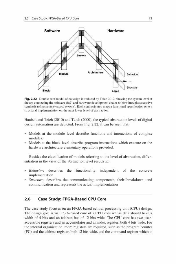
Haubelt and Teich (2010) and Teich (2000), the typical abstraction levels of digital
design automation are depicted. From Fig. 2.22, it can be seen that:
• Models at the module level describe functions and interactions of complex
modules.
• Models at the block level describe program instructions which execute on the
hardware architecture elementary operations provided.
Besides the classification of models referring to the level of abstraction, differ-
entiation in the view of the abstraction level results in:
• Behavior: describes the functionality independent of the concrete
implementation
• Structure: describes the communicating components, their breakdown, and
communication and represents the actual implementation
2.6 Case Study: FPGA-Based CPU Core
The case study focuses on an FPGA-based central processing unit (CPU) design.
The design goal is an FPGA-based core of a CPU core whose data should have a
width of 4 bits and an address bus of 12 bits wide. The CPU core has two user-
accessible registers and an accumulator and an index register, both 4 bits wide. For
the internal organization, more registers are required, such as the program counter
(PC) and the address register, both 12 bits wide, and the command register which is
Fig. 2.22 Double-roof model of codesign introduced by Teich 2012, showing the system level at
the top connecting the software (left) and hardware development chains (right) through successivesynthesis refinements (vertical arrows). Each synthesis step maps a functional specification onto a
structural implementation on the next lower level of abstraction
2.6 Case Study: FPGA-Based CPU Core 73
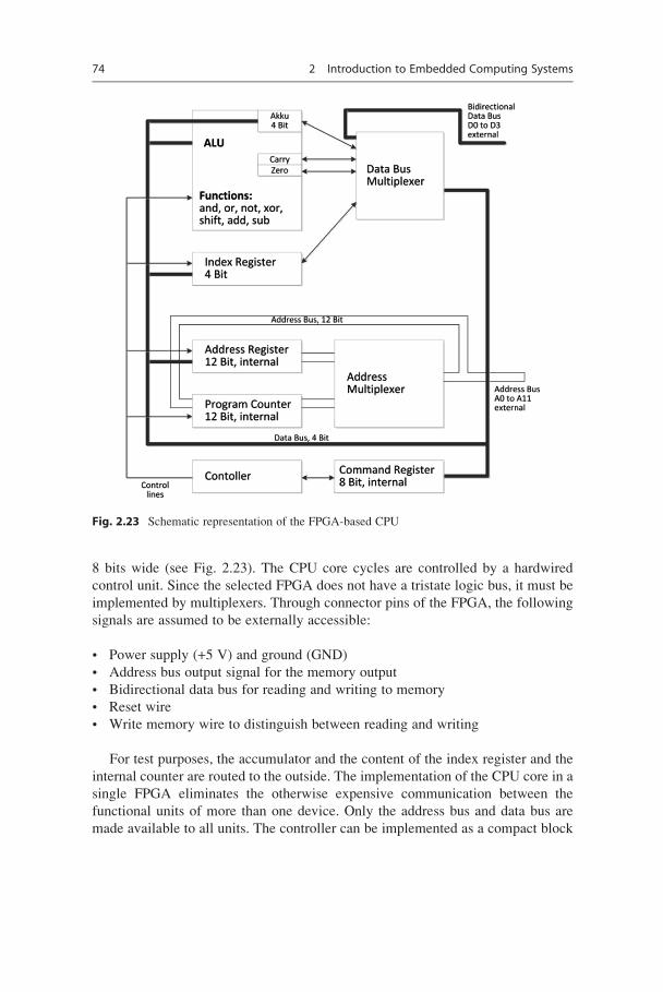
8 bits wide (see Fig. 2.23). The CPU core cycles are controlled by a hardwired
control unit. Since the selected FPGA does not have a tristate logic bus, it must be
implemented by multiplexers. Through connector pins of the FPGA, the following
signals are assumed to be externally accessible:
• Power supply (+5 V) and ground (GND)
• Address bus output signal for the memory output
• Bidirectional data bus for reading and writing to memory
• Reset wire
• Write memory wire to distinguish between reading and writing
For test purposes, the accumulator and the content of the index register and the
internal counter are routed to the outside. The implementation of the CPU core in a
single FPGA eliminates the otherwise expensive communication between the
functional units of more than one device. Only the address bus and data bus are
made available to all units. The controller can be implemented as a compact block
Fig. 2.23 Schematic representation of the FPGA-based CPU
74 2 Introduction to Embedded Computing Systems
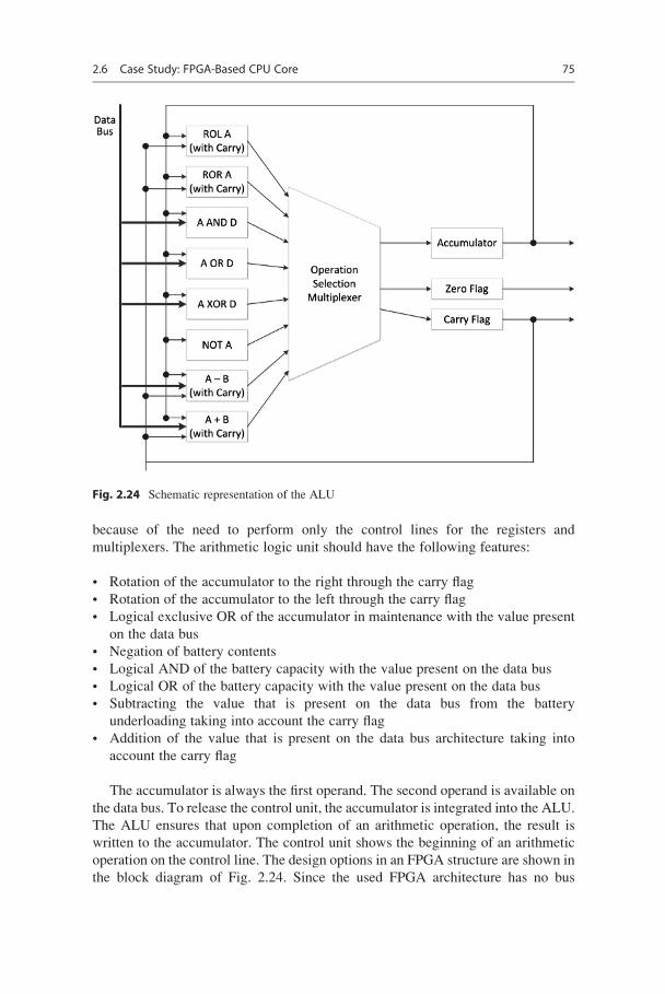
because of the need to perform only the control lines for the registers and
multiplexers. The arithmetic logic unit should have the following features:
• Rotation of the accumulator to the right through the carry flag
• Rotation of the accumulator to the left through the carry flag
• Logical exclusive OR of the accumulator in maintenance with the value present
on the data bus
• Negation of battery contents
• Logical AND of the battery capacity with the value present on the data bus
• Logical OR of the battery capacity with the value present on the data bus
• Subtracting the value that is present on the data bus from the battery
underloading taking into account the carry flag
• Addition of the value that is present on the data bus architecture taking into
account the carry flag
The accumulator is always the first operand. The second operand is available on
the data bus. To release the control unit, the accumulator is integrated into the ALU.
The ALU ensures that upon completion of an arithmetic operation, the result is
written to the accumulator. The control unit shows the beginning of an arithmetic
operation on the control line. The design options in an FPGA structure are shown in
the block diagram of Fig. 2.24. Since the used FPGA architecture has no bus
Fig. 2.24 Schematic representation of the ALU
2.6 Case Study: FPGA-Based CPU Core 75
structure, the selection of the function is realized with a multiplexer. All function
blocks shown in Fig. 2.24 are active. The control lines of the control unit only
decide whether/what result should be written. The eight functions of the ALU are
combined into groups of two, as two functions can be stored simultaneously in a
logic cell for 1 bit of the operand, reducing the space requirement by 50 %. More in
detail this is only the adder/subtractor block. In contrast to programmable logic
blocks where the adder is completely decoded, in the design example, a ripple-carry
adder is used, in which the carry bit is passed from bit to bit. This increases the time
the adder needs for a correct result but saves space. Thus, only two macrocells per
bit can be used for a ripple-carry adder.
With regard to the design requirements of the 4-bit CPU and an FPGA core
based on the instruction sets of existing processors, a minimal set has been selected
from the instruction set of the 8-bit CPU 6502. The instruction set chosen includes
the following command groups and commands:
• Transport commands: LDA LDX STA STX TAX TXA
• Arithmetic instructions: AND OR XOR ADD SUB ROL ROR NOT
• Branch instructions: JMP JC JNC JZ JNZ jxz JXNZ
• Other commands: NOP CLC DEX
An extension toward the 6502 microprocessor family instruction set is the
commands JXZ and JXNZ that allow a branch depending on the value of the X
register. The instruction word is stored in the memory in two parts, the high and low
nibbles. In the three stages of instruction decode, the corresponding sequence of a
22-bit wide control word is generated. Table 2.1 contains the hexadecimal codes for
each command (with all addressing modes), as well as information on the imple-
mentation and the duration (in cycles).
With the tabular program representation in Table 2.1, the conceptual, detailed
design of the FPGA CPU core is complete. Thereafter, the prototypical realization
by programming of the FPGA and the testing has to be done. The testing is
necessary because the correct programming of the module in the next programming
process may not always be fully verified. For this purpose, a simple test environ-
ment with the FPGA CPU core has to be built. The test environment consists of the
FPGA CPU core, an EPROM, a static RAM chip, a GAL, and a quartz crystal. The
reset of the input-output functions is implemented with the GAL. The test environ-
ment can be powered either by a quartz crystal oscillator or by a single-step circuit
with a clock. The test hardware has a reset button to access the CPU core in a
defined state. Through DIP switches, one of the test programs stored in the EPROM
can be selected. In addition, the test environment has seven-segment displays to
show the contents of the accumulator, index register, instruction register, address
bus, and data bus containing the display, so that the processing of individual
commands can be performed clock cycle by clock cycle.
76 2 Introduction to Embedded Computing Systems
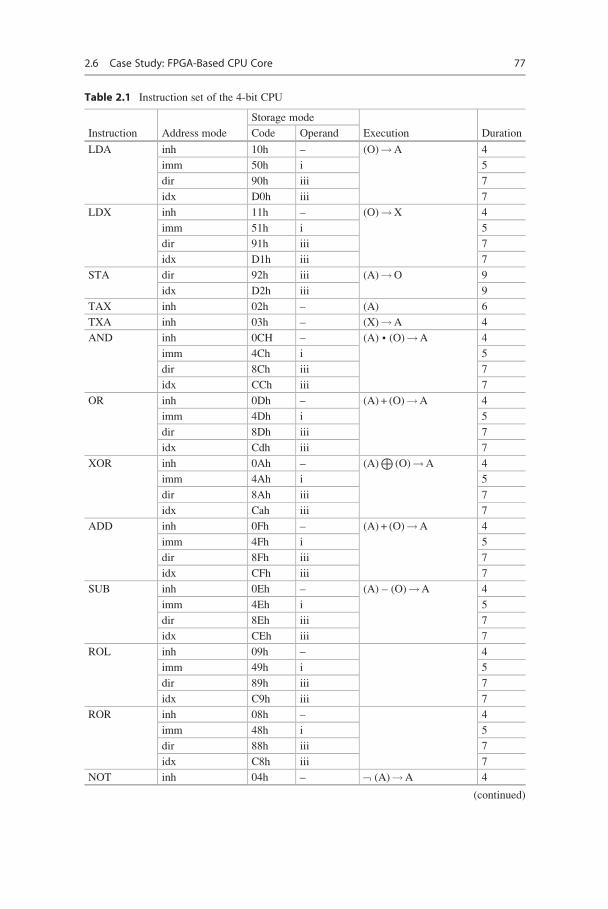
Table 2.1 Instruction set of the 4-bit CPU
Instruction Address mode
Storage mode
Execution DurationCode Operand
LDA inh 10h – (O)!A 4
imm 50h i 5
dir 90h iii 7
idx D0h iii 7
LDX inh 11h – (O)!X 4
imm 51h i 5
dir 91h iii 7
idx D1h iii 7
STA dir 92h iii (A)!O 9
idx D2h iii 9
TAX inh 02h – (A) 6
TXA inh 03h – (X)!A 4
AND inh 0CH – (A) • (O)!A 4
imm 4Ch i 5
dir 8Ch iii 7
idx CCh iii 7
OR inh 0Dh – (A) + (O)!A 4
imm 4Dh i 5
dir 8Dh iii 7
idx Cdh iii 7
XOR inh 0Ah – (A)L
(O)!A 4
imm 4Ah i 5
dir 8Ah iii 7
idx Cah iii 7
ADD inh 0Fh – (A) + (O)!A 4
imm 4Fh i 5
dir 8Fh iii 7
idx CFh iii 7
SUB inh 0Eh – (A) – (O)!A 4
imm 4Eh i 5
dir 8Eh iii 7
idx CEh iii 7
ROL inh 09h – 4
imm 49h i 5
dir 89h iii 7
idx C9h iii 7
ROR inh 08h – 4
imm 48h i 5
dir 88h iii 7
idx C8h iii 7
NOT inh 04h – Ø (A)!A 4
(continued)
2.6 Case Study: FPGA-Based CPU Core 77
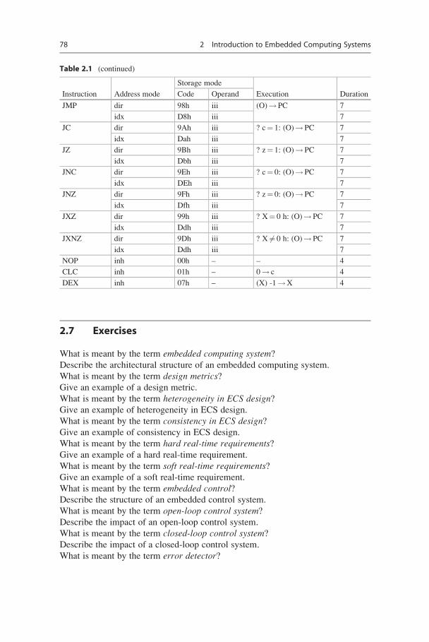
2.7 Exercises
What is meant by the term embedded computing system?Describe the architectural structure of an embedded computing system.
What is meant by the term design metrics?Give an example of a design metric.
What is meant by the term heterogeneity in ECS design?Give an example of heterogeneity in ECS design.
What is meant by the term consistency in ECS design?Give an example of consistency in ECS design.
What is meant by the term hard real-time requirements?Give an example of a hard real-time requirement.
What is meant by the term soft real-time requirements?Give an example of a soft real-time requirement.
What is meant by the term embedded control?Describe the structure of an embedded control system.
What is meant by the term open-loop control system?Describe the impact of an open-loop control system.
What is meant by the term closed-loop control system?Describe the impact of a closed-loop control system.
What is meant by the term error detector?
Table 2.1 (continued)
Instruction Address mode
Storage mode
Execution DurationCode Operand
JMP dir 98h iii (O)! PC 7
idx D8h iii 7
JC dir 9Ah iii ? c¼ 1: (O)! PC 7
7idx Dah iii
JZ dir 9Bh iii ? z¼ 1: (O)! PC 7
idx Dbh iii 7
JNC dir 9Eh iii ? c¼ 0: (O)! PC 7
idx DEh iii 7
JNZ dir 9Fh iii ? z¼ 0: (O)! PC 7
idx Dfh iii 7
JXZ dir 99h iii ? X¼ 0 h: (O)! PC 7
idx Ddh iii 7
JXNZ dir 9Dh iii ? X 6¼ 0 h: (O)! PC 7
idx Ddh iii 7
NOP inh 00h – – 4
CLC inh 01h – 0! c 4
DEX inh 07h – (X) -1!X 4
78 2 Introduction to Embedded Computing Systems
Describe the impact of an error detector.
What is meant by the term proportional controller?Describe the structure of a proportional controller.
What is meant by the term integral controller?Give an example of an integral controller.
What is meant by the term derivative controller?Give an example of a derivative controller.
What is meant by the term overshoot?Give an example of an overshoot.
What is meant by the term PID controller?Describe the impact of the PID time response characteristic.
What is meant by the term hardware/software codesign?Give an example of the workflow in hardware/software codesign.
What is meant by the term codesign?Describe the codesign process.
What is meant by the term target architecture?Give an example of target architecture.
What is meant by the term current HW/SW design process?Give an example of the workflow of the current HW/SW design process.
References and Further Reading
(Adamski et al. 2005) Adamski, M., A., Karatkevich, A., Wegrzyn, M.: Design of Embedded
Control Systems, Springer Publ. 2005
(Ashenden 2008) Ashenden P. J.: The Designers Guide to VHDL, Elsevier Publ. 2008
(Balarin et al. 2003) Balarin, F.: Metropolis: An Integrated Electronic \ Environment, Computer,
pp. 45–52, 2003
(Balasubramanian et al. 2006) Balasibramanian, K.: Developing Applications Using Model-
Driven Design Environments, Computer, pp. 33–40, 2006
(Booch et al. 2005) Booch, G., Rumbaugh, J., Jacobsen, I.: The Unified Modeling Language User
Guide, Pearson Higher Education Publ. 2005
(Chaturvedi 2010) Chaturvedi, D. K.: Modeling and Simulation of Systems Using MATLAB and
Simulink, CRC Press, 2010
(Colnaric and Verber 2008) Colnaric, M., Verber, D.: Distributed Embedded Control Systems,
Springer Publ. 2008
(Eker et al.2003) Eker, J.: Taming Heterogeneity: The Ptolemy Approach, Proc. IEEE, Vol. 91, no.
1, pp. 127–144, 2005
(Feiler and Gluch 2012) Feiler, P. H., Gluch, D. P.: Model-based Engineering with AADL: An
Introduction to the SAE Architecture Analysis and Design Language, Pearson Higher Educa-
tion Publ., 2012
(Haubelt and Teich 2010) Haubelt, C., Teich, J.: Digital Hardware/Software-Systems: Specifica-
tion and Verification (In German), Springer Publ. 2010
(Henzinger and Sifakis 2007) Henzinger T. A., Safakis, J.: Embedded Systems Design, IEEE
Computer Society, pp. 32–40, 2007
(Kamal 2008) Kamal, R.: Embedded Systems: Architecture, Programming, and Design, McGraw
Hill Publ. 2008
(Klee Allen 2011) Klee H., Allen, R.: Simulation of Dynamic Systems with Matlab and Simulink,
CRC Press, 2011
References and Further Reading 79
(Lee and Seisha 2015) Lee, E. A.; Seshia, S. A.: Introduction to Embedded Systems: A Cyber-
Physical Systems Approach, 2nd ed. Berkeley, CA, USA, 2015
(Moeller 2003) Moeller, D. P. F.: Mathematical and Computational Modeling and Simulation,
Springer Verlag, Berlin Heidelberg, 2003
(M€oller 2014) M€oller D. P. F.: Introduction to Transportation Analysis, Modeling and Simulation,
Springer Publ. Series Simulation Foundations, Methods, and Applications, 2014
(Oliveira, M. F. S., Redin, R. M.., Carro, L., da Cunha Lamb, L., Wagner, F. R.: Software Quality
Metrics and their Impact on Embedded Software. In: IEEE MOMPES 5th Internat. Workshop,
pp. 68–77, 2008,
(Perry 2002) Perry, D. L.: VHDL Programming by Example, McGraw Hill, 2002
(Plessel 2013) Plessel, C.: Hardware/Software Codesign; http://homepages.uni-paderborn.de/
plessl/lectures/2010-Codesign/script/Skript-Codesign.pdf. Accessed August 18, 2013
(Rockwell 2010) Rockwell, D.: State-Space Representation of LTI Systems, http://web.mit.edu/2.
14/www/Handouts/StateSpace.pdf
(Rumbaugh et al. 2004) Rumbaugh, J., Jacobsen, I., Booch, G.: The Unified Modeling Reference
Language Manual, Pearson Higher Education Publ., 2004
(Sciuto et al. 2003) Sciuto, D., Salice, F., Pomante, L., Fornaciari, W. : Metrics for Design Space
Exploration of Heterogeneous Multiprocessor Embedded Systems. http://pdf.aminer.org/000/
106/293/metrics_for_design_space_exploration_of_heterogeneous_multiprocessor_embed
ded_systems.pdf
(Sifakis 2005) Sifakis J.: A Framework for Component-Based Construction, Proc. Software Eng.
and Formal Methods, IEEE, pp. 293–300, 2005
(Teich 2000) Teich, J.: Embedded system synthesis and optimization. In: Proc. Workshop Systems
Design Automation, pp. 9–22, Rathen, Germany, 2000
(Teich 2012) Teich, J.: Hardware/Software Codesign: The Past, the Present, and Predicting the
Future; Proceedings of the IEEE, Vol. 100, pp. 1411–1430, 2012
(Vahid and Lysecky 2007) Vahid, F., Lysecky, R.: Verilog for Digital Design, John Wiley Publ.
2007
(Visioli 2006) Visioli, A.: Practical PID Control, Springer Publ. 2006
(Zurawski 2009) Zurak, R.: Embedded Systems Handbook, CRC Publ., 2009
80 2 Introduction to Embedded Computing Systems

http://www.springer.com/978-3-319-25176-9