Embed Size (px)
Citation preview
INXS: Bridging the Throughput and Energy Gapfor Spiking Neural Networks
Surya NarayananSchool of Computing
University of Utah
Ali ShafieeSchool of Computing
University of Utah
Rajeev BalasubramonianSchool of Computing
University of Utah
Abstract—In recent years, multiple neuromorphic architectures have
been designed to execute cognitive applications that deal withimage and speech analysis. These architectures have followedone of two approaches. One class of architectures is based onmachine learning with artificial neural networks. A second classis focused on emulating biology with spiking neuron models, in anattempt to eventually approach the brain’s accuracy and energyefficiency. A prominent example of the second class is IBM’sTrueNorth processor that can execute large spiking networkson a low-power tiled architecture, and achieve high accuracyon a variety of tasks. However, as we show in this work, thereare many inefficiencies in the TrueNorth design. We proposea new architecture, INXS, for spiking neural networks thatimproves upon the computational efficiency and energy efficiencyof the TrueNorth design by 3,129× and 10× respectively. Thearchitecture uses memristor crossbars to compute the effects ofinput spikes on several neurons in parallel. Digital units are thenused to update neuron state. We show that the parallelism offeredby crossbars is critical in achieving high throughput and energyefficiency.
I. INTRODUCTION
The stagnation of Moore’s Law scaling has shifted industryand academia’s focus away from general-purpose systems andtowards specialized systems. Neuromorphic architectures arean important class of specialized systems because:
1) They are efficient at a variety of machine learning tasksthat are growing in prominence – image analysis inself driving cars, information discovery from massivedatasets, etc.
2) They target the grand challenge of emulating brain me-chanics in hopes of matching the brain’s cognitive powerand energy efficiency.
These two separate needs – machine learning efficiencyand brain emulation – have also led to a bifurcation inneuromorphic architectures.
A number of architectures, DaDianNao [8], ISAAC [37],EIE [38], Cnvlutin [3], and Eyeriss [7] to name a few, arebased on the artificial neurons (perceptrons) that have formedthe basis for decades of research in machine learning. We referto these architectures as artificial neural network accelerators,or ANN accelerators.
The second class of architectures, TrueNorth [2], SpiN-Naker [25], and Neurogrid [4] to name a few, are based onbiologically plausible models of spiking neurons. We refer to
these architectures as spiking neural network accelerators, orSNN accelerators.
The goal of this paper is not to compare ANN vs. SNNaccelerators. To date, only one study, by Du et al. [13],has performed a head-to-head comparison of ANN and SNNaccelerators. While that study is an excellent start to an impor-tant debate, it draws limited conclusions for small-scale chipsexecuting small-scale networks. For example, they concludethat SNNs achieve significantly lower accuracy than ANNson MNIST, but concurrent work [14, 15] developed bettertraining algorithms for SNNs and achieved 99.42% accuracyon MNIST. Du et al. investigate chips with no more than 110artificial neurons and 300 spiking neurons. We mention theseexamples to highlight that the comparison between ANNs andSNNs is far from being resolved, and will likely play out overthe coming decade.
In the meantime, advances are required for both ANNs andSNNs. At the moment, much of the architecture research hasfocused on ANNs. As a result, ANNs are ahead of SNNson a variety of metrics (see Table I). This paper attempts tobridge that gap by designing better SNN architectures that cankeep up with the high throughput and energy efficiency beingachieved on state-of-the-art ANNs.
The most high-profile and most efficient SNN architectureto date is IBM’s TrueNorth. It is a 5.4 billion transistor chipthat can model 1 million neurons and 256 million synapseswhile consuming less than 100 mW. TrueNorth achieves hightile-level parallelism, and makes a number of design choicesthat impose constraints on the application, while reducingpower and storage requirements. However, we see in Table Ithat TrueNorth lags behind state-of-the-art ANN acceleratorson all metrics, notably throughput and energy. Therefore,drawing inspiration from recent ANN architectures, we un-dertake an overhaul of the TrueNorth design.
We describe an SNN accelerator that leverages memristorcrossbars to aggregate the effects of input spikes in the analogdomain. By effectively using in-situ computing, memristorcrossbars have been shown to achieve high parallelism andstorage density in the ISAAC [37] and PRIME [9] ANNaccelerators. We describe the many changes required to adapt acrossbar-based architecture for an SNN. In particular, the man-agement of neuron potentials represents the biggest challenge,and the sparse spike rate represents the biggest opportunity.The former requires additional storage overheads, and the
Network Type Accuracy Throughput (TOPs/s) Energy per operation (pJ/op)MNIST CIFAR-10 AlexNet Digital Analog Digital Analog
ANN 99.77% [10] 96.53% [17] 89% [26] 9 [3, 8] 45 [37] 3.2 [3, 8] 1.5 [37]SNN 99.42% [14] 89.32% [15] 82.5% [21] 0.058 [2] 0.07 [29] 41 [2] 0.35 [29]
TABLE ICOMPARISON OF ACCURACY, THROUGHPUT, AND ENERGY EFFICIENCY FOR STATE-OF-THE-ART ANNS AND SNNS. THE DIGITAL SNN NUMBERS
CORRESPOND TO TRUENORTH [2]. THE ENERGY NUMBER FOR THE ANALOG SNN ACCELERATOR IS FOR A SMALL-SCALE 32-NEURONIMPLEMENTATION [29].
latter enables low overheads for analog-to-digital conversion(ADC). We carry out a design space exploration to identifythe best provisioning of resources for this mixed-signal archi-tecture.
II. BACKGROUND
Artificial neurons were developed more than 70 yearsago [30]. Artificial neurons receive synchronous real-valuedinputs, perform a dot-product of these inputs with weights,apply an activation function (often ReLU), and pass real-valued outputs to the next layer of artificial neurons. Inaddition to many decades of progress, the past decade has seensignificant advances with artificial neurons, primarily becauseof our ability to train deep networks with a combination ofnew techniques.
A. Spiking Neurons
While neuroscientists have delved into the mechanics ofthe biological neuron for decades [20], it has only recentlyreceived attention from the architecture community. A numberof high-profile projects [2, 4, 25] have attempted to implementbiologically plausible neuron models in hardware. Many ofthese hardware projects implement neuron models that arehighly simplified, but that can emulate many biologicallyobserved neuron behaviors, e.g., the Izhikevich neurons [34].
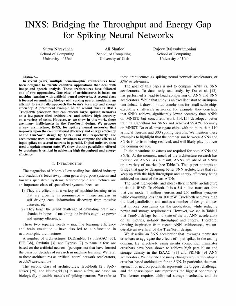
The most popular of these simple neuron models is theLinear Leaky Integrate and Fire model (LLIF), shown inFigure 1. An LLIF neuron is stateful – in addition to synapticweights, it retains the value of its (membrane) potential. Thispotential reflects inputs that have been received in the recentpast. Inputs are received in the form of binary spikes. Whena spike is received on an input, the synaptic weight for thatinput is added to the potential (see Figure 1). In every cycle, aleak is also subtracted from the potential. When the neuron’spotential eventually reaches a specified threshold, the neuronproduces an output spike of its own. After the spike, the neuronpotential is reset.
Spiking neurons have the potential to be hardware-efficientbecause inputs and outputs are binary spikes, i.e., a communi-cation link between neurons requires a single bit. Further, thespiking neuron model does not require a multiplier – becausethe input is binary, the synaptic weight is simply added to thepotential. Spikes can therefore lead to efficient communicationand computation.
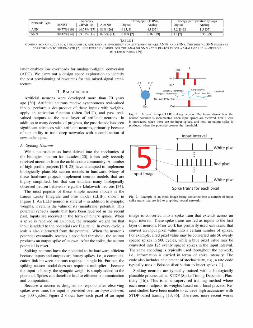
Because a neuron is designed to respond after observingspikes over time, the input is provided over an input interval,say 500 cycles. Figure 2 shows how each pixel of an input
In 1 In 2
Out
In 1
In 2
Out
Time
Neuron Potential
Output spike
LeakWeight 1 increment
Weight 2 incrementReset potential
Threshold
Fig. 1. A basic 2-input LLIF spiking neuron. The figure shows how theneuron potential is incremented when input spikes are received, how a leakis subtracted when there are no input spikes, and how an output spike isproduced when the potential crosses the threshold.
……
Input Interval
Spike trains for each pixel
White pixel
White pixel
Red pixel
Input Image
Fig. 2. Example of an input image being converted into a number of inputspike trains that are fed to a spiking neural network.
image is converted into a spike train that extends across aninput interval. These spike trains are fed as inputs to the firstlayer of neurons. Prior work has primarily used rate codes thatconvert an input pixel value into a certain number of spikes.For example, a red pixel value may be converted into 50 evenlyspaced spikes in 500 cycles, while a blue pixel value may beconverted into 125 evenly spaced spikes in the input interval.The same encoding is typically used throughout the network,i.e., information is carried in terms of spike intensity. Thecode also includes an element of stochasticity, e.g., a rate codetypically uses a Poisson distribution to inject spikes [1].
Spiking neurons are typically trained with a biologicallyplausible process called STDP (Spike Timing Dependent Plas-ticity [16]). This is an unsupervised training method whereeach neuron adjusts its weights based on a local process. Re-cent studies have been unable to achieve high accuracies withSTDP-based training [13, 36]. Therefore, more recent works
have resorted to supervised backpropagation-based training forspiking networks [14, 15].
B. SNN Accelerators
IBM’s TrueNorth processor [32] is the most prominentexample of a digital architecture for large SNNs. We willuse TrueNorth as the SNN baseline in this work because itachieves best-in-class throughput and energy efficiency.
TrueNorth is composed of many tiles, where each tileimplements 256 neurons, each with 256 inputs. The tilescommunicate through an on-chip and potentially an off-chipnetwork. The tiles use a mix of asynchronous and synchronouscircuits to boost energy efficiency. In every 1ms “tick”, a tileprocesses all received input spikes; any resulting output spikesare sent through the network to neurons in the next layer sothey can be processed in a subsequent tick. TrueNorth imple-ments an LLIF neuron model with a number of configurableparameters, including some that allow stochastic behavior.Within a tick, the tile sequentially walks through every neuronin that tile and every input spike to perform several updatesto each neuron potential. For each neuron, it reads a 410-bit SRAM row that contains all parameters for that neuron,including a 256-bit vector indicating which tile inputs connectto that neuron. This bit vector is reconciled with the list ofinput spikes in that tick to identify spiking connections forthat neuron. The synaptic weight for each of these connectionsis then sent to a synchronous neuron unit that performs thenecessary arithmetic operations. This unit adds the synapticweights to the neuron’s potential. Finally, the leak is subtractedand the potential is compared against the threshold. In case ofan output spike, the neuron potential is reset. The final neuronpotential is then written back to the SRAM bank. The 12.8 KBSRAM bank occupies nearly half the tile area and one-thirdthe tile power. A tile processes a single synapse at a time. Thetick is long enough (1ms) to process all possible input spikesand neurons sequentially.
To further reduce storage requirements and energy,TrueNorth imposes several constraints on the neural network.It only uses 4 quantized 9-bit weights per neuron. It also forcesan input spike to share the same weight type with all neuronsin that tile. A neuron’s output can only be seen by the 256neurons in one tile. A neuron can only receive at most 256inputs.
SpiNNaker [25] is another prominent SNN architecture thatuses many low-power general-purpose ARM cores to performseveral parallel neuron updates. It is well known that customASICs will out-perform general-purpose cores by at least twoorders of magnitude [18], so we will not explore SpiNNaker-style architectures in this paper.
A few projects have attempted to implement neurons andsynapses with analog devices, typically using capacitors ormemristors to emulate neuronal behavior [2, 28, 29, 42]. Theseprojects have focused more on device innovations to repro-duce neuron behavior, and have not focused on architecturalinnovations to boost throughput. For example, Liu et al. [29]implement a single 32×64 memristive crossbar to execute
feedforward and Hopfield networks. The crossbar performsthe synaptic operations, and an analog integrate-and-fire circuitmodels the neuron. But, maintaining the neuron potential in ananalog circuit can incur a very high area overhead, especiallyin large-scale convolutional networks where the number ofneurons far exceeds the number of (shared) synapses. How-ever, we do believe that analog circuits have a lot to offer [23]and we will use the analog domain in a limited manner toaccelerate the neuron update.
C. ANN Accelerators
Our proposed architecture is inspired by the best practices instate-of-the-art ANN accelerators. We first discuss the analogapproach, followed by the digital approach.
S+H S+H S+H S+H
ADC
S+A
Conductance W1
W2
W3
W4
X2
X3
X4
Current X1W1
Voltage X1
X1W1+X2W2
X1W1+X2W2+X3W3+X4W4
X1W1+X2W2+X3W3
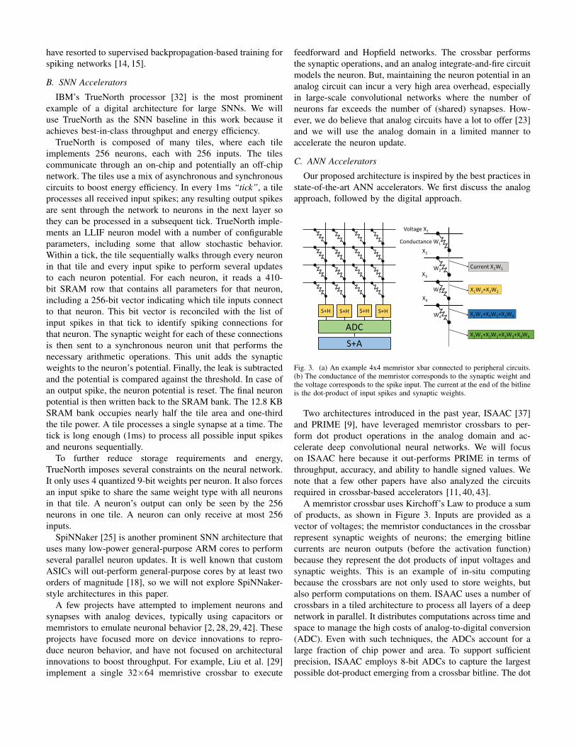
Fig. 3. (a) An example 4x4 memristor xbar connected to peripheral circuits.(b) The conductance of the memristor corresponds to the synaptic weight andthe voltage corresponds to the spike input. The current at the end of the bitlineis the dot-product of input spikes and synaptic weights.
Two architectures introduced in the past year, ISAAC [37]and PRIME [9], have leveraged memristor crossbars to per-form dot product operations in the analog domain and ac-celerate deep convolutional neural networks. We will focuson ISAAC here because it out-performs PRIME in terms ofthroughput, accuracy, and ability to handle signed values. Wenote that a few other papers have also analyzed the circuitsrequired in crossbar-based accelerators [11, 40, 43].
A memristor crossbar uses Kirchoff’s Law to produce a sumof products, as shown in Figure 3. Inputs are provided as avector of voltages; the memristor conductances in the crossbarrepresent synaptic weights of neurons; the emerging bitlinecurrents are neuron outputs (before the activation function)because they represent the dot products of input voltages andsynaptic weights. This is an example of in-situ computingbecause the crossbars are not only used to store weights, butalso perform computations on them. ISAAC uses a number ofcrossbars in a tiled architecture to process all layers of a deepnetwork in parallel. It distributes computations across time andspace to manage the high costs of analog-to-digital conversion(ADC). Even with such techniques, the ADCs account for alarge fraction of chip power and area. To support sufficientprecision, ISAAC employs 8-bit ADCs to capture the largestpossible dot-product emerging from a crossbar bitline. The dot
products, after analog to digital conversion, are aggregatedwith digital ALUs. eDRAM banks are used to store neuronoutputs until they are consumed by the next layer. By settingup a pipeline from layer to layer, a relatively small set ofoutputs has to be buffered, which can be accommodated ina 64 KB eDRAM unit per tile. Since a dense crossbar isused to store the weights and perform computation, ISAACis able to dramatically reduce data movement, and increasecomputation/storage density.
We next describe recent digital ANN architectures. TheDianNao [6] and DaDianNao [8] accelerators were amongthe first to target deep convolutional networks. DianNao de-signs the digital circuits for a basic NFU (Neural FunctionalUnit) that can process 16 inputs to 16 neurons in parallel.DaDianNao is a tiled architecture where each tile has anNFU and eDRAM banks that feed synaptic weights to thatNFU. DaDianNao uses many tiles on many chips to parallelizethe processing of a single network layer. Once that layer isprocessed, all the tiles then move on to processing the nextlayer in parallel. Thus, the keys to DaDianNao’s efficiencyare: (i) localized data movement (from local eDRAM bank tonearby NFU), and (ii) time-multiplexed execution of severalneurons and several network layers on a small set of SIMDexecution units (the NFUs). Other recent papers have proposedinnovations to digital ANN accelerators that primarily exploitsparsity [3, 35, 38]. Since digital ANN accelerators are nearlyan order of magnitude slower than ISAAC [37], we will notconsider them further in this paper.
III. THE INXS ARCHITECTURE
A. Overview
As described in the previous section, the best SNN accel-erator to date, TrueNorth, suffers from a few weaknesses:
1) There is no intra-tile parallelism while performing neuronupdates.
2) Each input spike to a neuron is handled sequentially.3) To reduce the storage and energy overheads, significant
approximations have to be made for the synaptic weightvalues.
4) A neuron can only have at most 256 inputs and its outputcan be seen by at most 256 other neurons connected toone axon.
We design a mixed-signal architecture, INXS1, that ad-dresses all of the above problems, and can efficiently handlestate-of-the-art deep networks. A large number of memristorcrossbars are used to process the many incoming spikes ina tick, and compute the resulting potential increments inparallel. The potential increments are immediately converted todigital signals. The neuron potentials are retrieved from SRAMbuffers with wide reads, added to the increments, thresholded,and written back to SRAM. The resulting spikes are routedto the next layers so they can be processed in the next tick.Many crossbars work in unison on different layers of the neuralnetwork to set up an efficient pipeline.
1INXS, pronounced “in excess” is short for IN-situ Xbar Spiking
The key contributions of this design are:1) It offers very high pipelined parallelism with many cross-
bars, not only working on many SNN layers in parallel(as in TrueNorth), but also working on many neuronupdate values and many input spikes in parallel (unlikeTrueNorth). In most cases, the pipeline operates as anodd-even pipeline, working on analog crossbar operationsin odd ticks, and digital neuron updates in even ticks.
2) While some prior works [29] have implemented a cross-bar in tandem with analog neurons, we observe herethat in a convolutional network, a set of shared weightsare used to compute several neurons. The use of analogneurons would require a single crossbar bitline to bemultiplexed across many analog circuits, resulting in sig-nificant overheads. Therefore, we immediately convert theanalog crossbar output into a digital signal and performthe even phase in the digital domain.
3) We lay out several design details and carefully considerthe overheads of each module. We follow with a designspace exploration to identify how best to provision theresources per tile.
4) The resulting architecture differs from the state-of-the-art ANN accelerator, ISAAC, in the following ways: (i)ISAAC requires a 22-stage pipeline while INXS onlyrequires a 2-stage pipeline to process a single neuron inone layer, (ii) INXS uses a low-resolution ADC becauseof observed sparsity, thus achieving higher throughput perarea, and (iii) it allocates more area for central storageand neuron update.
5) The resulting architecture differs from the state-of-the-art SNN accelerator, TrueNorth, in the following ways:(i) INXS does not constrain neuron input/outputs andweights in any way, (ii) it offers orders of magnitudehigher parallelism and throughput, and (iii) it achieveslower energy per operation by boosting throughput andlowering the contribution of leakage.
B. Implementation Details
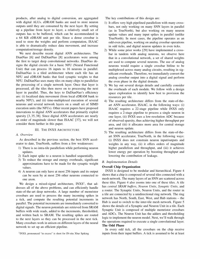
Overall Chip OrganizationINXS is designed to be modular and hierarchical. Figure 4
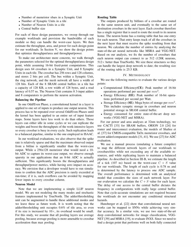
shows that a chip is composed of several tiles connected with amesh network. The many layers of an SNN are scattered acrossthese tiles. Figure 4 also zooms into one of these tiles. A tilehas central SRAM buffers, Neuron Units, Synaptic Units, anda router. The Synaptic Units, Neuron Units, and the router ina tile are connected by a unidirectional ring network. The ringnetwork has North, South, East, West, and Hub stations – theHub is used to switch to the inter-tile mesh network. Figure 5shows the details of a Synaptic and Neuron Unit in a tile. EachSynaptic Unit is composed of multiple memristor crossbarsand ADCs. The Neuron Unit has the adders and thresholdinglogic to implement the neuron model. Next, we’ll walk throughthe operations required to execute a single convolutional layer.The Odd Phase
In every odd tick, all the crossbars on the chip receiveinputs from their input buffers. A tick is assumed to be at least
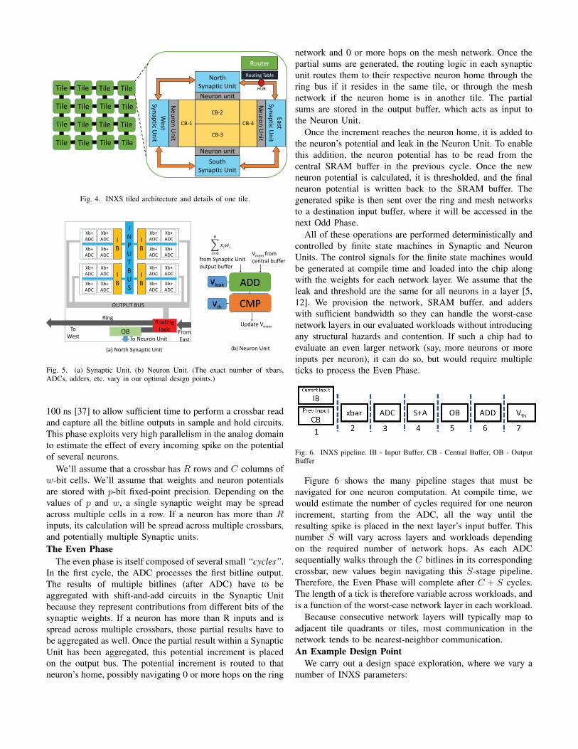
CB-1 CB-4
South
Synaptic Unit
North
Synaptic Unit
Ea
st
Sy
na
ptic U
nit
We
st
Sy
na
ptic U
nit
Ne
uro
n U
nit
Ne
uro
n U
nit
Neuron unit
Neuron unit
Routing Table
Router
Tile
Tile
Tile
Tile
Tile
Tile
Tile
Tile
Tile
Tile
Tile
Tile
Tile
Tile
Tile
Tile
CB-2
CB-3
HUB
Fig. 4. INXS tiled architecture and details of one tile.
I
B
Xb+
ADC
I
B
I
B
I
B
I
N
P
U
T
B
U
S
Ring
OUTPUT BUS
Routing
logicOB
ADD
CMP
Vleak
Vth
Update Vmem
(b) Neuron Unit(a) North Synaptic Unit
Vmem from
central buffer from Synaptic Unit
output buffer
To
WestFrom
EastTo Neuron Unit
Xb+
ADC
Xb+
ADC
Xb+
ADC
Xb+
ADC
Xb+
ADC
Xb+
ADC
Xb+
ADC
Xb+
ADC
Xb+
ADC
Xb+
ADC
Xb+
ADC
Xb+
ADC
Xb+
ADC
Xb+
ADC
Xb+
ADC
Fig. 5. (a) Synaptic Unit. (b) Neuron Unit. (The exact number of xbars,ADCs, adders, etc. vary in our optimal design points.)
100 ns [37] to allow sufficient time to perform a crossbar readand capture all the bitline outputs in sample and hold circuits.This phase exploits very high parallelism in the analog domainto estimate the effect of every incoming spike on the potentialof several neurons.
We’ll assume that a crossbar has R rows and C columns ofw-bit cells. We’ll assume that weights and neuron potentialsare stored with p-bit fixed-point precision. Depending on thevalues of p and w, a single synaptic weight may be spreadacross multiple cells in a row. If a neuron has more than Rinputs, its calculation will be spread across multiple crossbars,and potentially multiple Synaptic units.The Even Phase
The even phase is itself composed of several small “cycles”.In the first cycle, the ADC processes the first bitline output.The results of multiple bitlines (after ADC) have to beaggregated with shift-and-add circuits in the Synaptic Unitbecause they represent contributions from different bits of thesynaptic weights. If a neuron has more than R inputs and isspread across multiple crossbars, those partial results have tobe aggregated as well. Once the partial result within a SynapticUnit has been aggregated, this potential increment is placedon the output bus. The potential increment is routed to thatneuron’s home, possibly navigating 0 or more hops on the ring
network and 0 or more hops on the mesh network. Once thepartial sums are generated, the routing logic in each synapticunit routes them to their respective neuron home through thering bus if it resides in the same tile, or through the meshnetwork if the neuron home is in another tile. The partialsums are stored in the output buffer, which acts as input tothe Neuron Unit.
Once the increment reaches the neuron home, it is added tothe neuron’s potential and leak in the Neuron Unit. To enablethis addition, the neuron potential has to be read from thecentral SRAM buffer in the previous cycle. Once the newneuron potential is calculated, it is thresholded, and the finalneuron potential is written back to the SRAM buffer. Thegenerated spike is then sent over the ring and mesh networksto a destination input buffer, where it will be accessed in thenext Odd Phase.
All of these operations are performed deterministically andcontrolled by finite state machines in Synaptic and NeuronUnits. The control signals for the finite state machines wouldbe generated at compile time and loaded into the chip alongwith the weights for each network layer. We assume that theleak and threshold are the same for all neurons in a layer [5,12]. We provision the network, SRAM buffer, and adderswith sufficient bandwidth so they can handle the worst-casenetwork layers in our evaluated workloads without introducingany structural hazards and contention. If such a chip had toevaluate an even larger network (say, more neurons or moreinputs per neuron), it can do so, but would require multipleticks to process the Even Phase.
Fig. 6. INXS pipeline. IB - Input Buffer, CB - Central Buffer, OB - OutputBuffer
Figure 6 shows the many pipeline stages that must benavigated for one neuron computation. At compile time, wewould estimate the number of cycles required for one neuronincrement, starting from the ADC, all the way until theresulting spike is placed in the next layer’s input buffer. Thisnumber S will vary across layers and workloads dependingon the required number of network hops. As each ADCsequentially walks through the C bitlines in its correspondingcrossbar, new values begin navigating this S-stage pipeline.Therefore, the Even Phase will complete after C + S cycles.The length of a tick is therefore variable across workloads, andis a function of the worst-case network layer in each workload.
Because consecutive network layers will typically map toadjacent tile quadrants or tiles, most communication in thenetwork tends to be nearest-neighbor communication.An Example Design Point
We carry out a design space exploration, where we vary anumber of INXS parameters:
• Number of memristor xbars in a Synaptic Unit• Number of Synaptic Units in a tile• Number of Neuron Units in a tile• Central buffer size
For each of these design parameters, we sweep through ourexample workloads and provision the bandwidths of eachmodule so they can handle the worst-case layers. We thenestimate the throughput, area, and power for each design pointfor our workloads. In Section V, we show the design pointsthat optimize throughput/area and throughput/power.
To make our architecture more concrete, we walk throughthe parameters selected for the optimal throughput/area designpoint, while assuming 16-bit fixed-point computations. Thisdesign uses 64 crossbars in a Synaptic Unit, and 8 SynapticUnits in each tile. The crossbar has 256 rows and 128 columns,and stores 2 bits per cell. The bus within a Synaptic Unit,the ring network, and the mesh network all have a width of128 bits. Each of the 8 SRAM central buffers in a tile hasa capacity of 128 KB, a row width of 128 bytes, and a readlatency of 0.57 ns. The Neuron Unit contains 8 3-input addersand 8 comparators to perform the neuron activation.Balancing the Pipeline
In one Odd/Even Phase, a convolutional kernel in a layer isapplied to one set of inputs to produce one output neuron. Thisprocess has to be repeated over several Odd/Even Phases untilthe kernel has been applied to an entire set of input featuremaps. Some layers have less work to do than others. Thoselayers can either idle in some cycles or we can replicate theweights and boost the throughputs of the work-intensive layersso every crossbar is busy in every cycle. Such replication leadsto a balanced pipeline, similar to the one employed in ISAAC.
In our workload evaluations, we also observe that the spikerate is relatively sparse and that the maximum observed outputfrom a bitline is significantly smaller than the worst-caseoutput. While a 256x128 memristor xbar would need a 10-bit ADC to capture its worst-case output, we observe enoughsparsity in our applications that an 8-bit ADC is actuallysufficient. This significantly boosts the throughput/area andthroughput/power metrics, while having zero impact on accu-racy. We envision that a developer would have to run simula-tions to confirm that the ADC precision is rarely exceeded atrun-time; if it is, such overflows can be avoided by mappingfewer inputs to every crossbar column.Neuron Model
Note that we are implementing a simple LLIF neuronmodel. We are not modeling the many modes and stochasticfeatures implemented by TrueNorth. The adder/thresholdingunit can be augmented to handle these additional modes andwe leave these as future work. It is worth noting that theadder/thresholding unit occupies 0.6% of tile area, so evenif its size is increased by 10×, its overhead would be small.For this study, we assume that all pooling layers use averagepooling, because average pooling is more amenable to crossbaracceleration than max pooling.
Routing TableThe outputs produced by bitlines of a crossbar are routed
to the same neuron unit, and eventually to the same set ofdestination crossbars in the next layer. Each crossbar thereforehas a single register that is used to route the result to its neuronhome. The neuron home has a routing table that has one entryfor each neuron. That entry keeps track of all the crossbars inthe next layer that must receive the spike resulting from thatneuron. We calculate the number of entries by analyzing thestate-of-the-art neural networks like MSRA and VGG-NET.Based on our analysis, we fix the number of crossbars thateach neuron output can connect to as 512 (128K neurons,512× better than TrueNorth). We size these structures so theycan handle the largest deep network to date; the resulting sizeof the routing table is 25.5 KB.
IV. METHODOLOGY
We use the following metrics to evaluate the various designpoints:
• Computational Efficiency(CE): Peak number of 16-bitoperations performed per second per mm2.
• Energy Efficiency (EE): Peak number of 16-bit opera-tions performed per second per Watt.
• Storage Efficiency (SE): Mega bytes of storage per mm2.This includes synaptic storage in crossbars and neuronpotential storage in SRAM central buffer.
• Energy consumed for entire state-of-the-art deep net-works (VGG-NET and MSRA).
For our power and area analyses at 32nm technology, weuse CACTI [33] for SRAM buffers, ORION 2.0 [24] forrouter and interconnect evaluation, the models of Shafiee etal. [37] for CMOS-compatible TaOx memristor crossbars, andrecent adder/comparator models [31, 41]. We use [27] for ADCevaluation.
We use a manual process (emulating a future compiler)to map the different network layers of our workloads tocrossbars/tiles while not exceeding any of the available re-sources, and while replicating layers to maintain a balancedpipeline. As described in Section III-B, we estimate the lengthof a tick (107 ns) based on the worst-case C + S valuefor our workloads. The length of each cycle is 0.78 ns andis determined by the latency to process one ADC sample.The overall performance is determined with an analyticalmodel that considers the sizes of each network layer. Forour evaluvation we calculate the C + S value for each layer.The delay of one access to the central buffer dictates thefrequency in configurations with really large central buffer.Note that cycle-accurate simulations are not required becausethe workloads do not encounter any conditional structuralhazards.
Hunsberger et al. [22] show that convolutional neural net-works can be mapped to SNNs while achieving very sim-ilar accuracy. In a similar vein, we use two state-of-the-artdeep convolutional networks for image classification, VGG-NET [39] and MSRA [19], to evaluate INXS. Since we need tofind a design point that performs well on both fully connected
SNNs and convolutional SNNs, we pick VGG-NET (it hasthe most neurons/layer in Conv1) and MSRA (it has the mostnumber of inputs/neuron in FC1).
ISAAC uses a 128×128 crossbar and an 8-bit ADC sobits are never dropped. The use of a modest crossbar sizekeeps noise in check and allows use of a low-resolution ADC.Given the inherent sparsity of spikes in an SNN, we allow useof a 256×128 crossbar while still using an 8-bit ADC. Wealso explore the use of a 6-bit ADC that assumes sufficientsparsity in spikes. Note that applications with high spike rateswould be forced to use a subset of crossbar rows so the ADCprecision is rarely exceeded. As a sensitivity study, we alsoexplore use of a 6-bit ADC in tandem with 1-bit memristorcells that is guaranteed to not drop bits – while this designhas a lower overhead for ADCs, it uses more crossbars torepresent synaptic weights. Our results show that this designpoint does not match a design with an 8-bit ADC in tandemwith 2-bit memristor cells, so we will not discuss it further.
V. RESULTS
A. INXS design space exploration
For all our results, we evaluate metrics across a numberof design points. The X-axis in most figures describes thesedesign points as a×b×c×d, where a×b describes the numberof crossbars in a Synaptic Unit, c represents the number ofSynaptic Units per tile, and d represents the capacity of centralbuffer in a tile (in KB). Note that in a convolutional layer, asingle crossbar can produce results for several neurons acrossseveral ticks. The size of the central buffer puts a cap onthe number of neurons that can be produced locally by thecorresponding synaptic units.
We first evaluate peak computational efficiency, shownin Figure 7, for the INXS design as we vary our designparameters. Similarly, Figures 8 and 9 quantify the EE andSE metrics respectively. The main observation from thesefigures is that all these metrics improve when the central buffersize is reduced. This is because peak metrics are primarilyimpacted by the number of crossbars, which offer high storageand computation. Note that SE is a sum of neuron andsynaptic density. Providing a large SRAM buffer increasesneuron density (and is helpful to convolutional layers), butdecreases synaptic density (not helpful to fully connectedlayers). Clearly, the latter effect is more dominant in thisanalysis of peak performance, so we see a drop in SE whenCB size is increased. Figure 10 further breaks the SE metricinto neuron and synaptic density.
While peak CE, EE, and SE are useful metrics and favorcrossbar computation over neuron potential storage, deepnetworks with large convolutional layers benefit more fromneuron potential storage. Therefore, ultimately, we need toevaluate INXS designs on state-of-the-art deep networks, e.g.,VGG and MSRA. Figures 11 and 12 show the energy fordifferent design points for these two workloads. These realworkloads exhibit the best metrics when using larger cen-tral buffer sizes. Based on this analysis, we pick an idealdesign point that does reasonably well for both workloads:
Fig. 7. Computational efficiency of INXS for various configurations.
Fig. 8. Energy efficiency of INXS for various configurations.
Fig. 9. Storage efficiency of INXS for various configurations.
Fig. 10. M-synapses/mm2 and K-Neurons/mm2 for various INXS configu-rations.
8x8x8x128. For this ideal design point, Figures 13 and 14show a breakdown of the area and energy required by thedifferent layers of the deep networks. Table II summarizes thearea and power of each component in an INXS tile.
Contrary to what we saw earlier for peak CE, EE, andSE metrics, the configurations with large central buffer per-form well on MSRA and VGG-NET. The reason for this isthe overhead of inter-tile and intra-tile interconnect energy.Configurations with small central buffers engage in moreintra- and inter-tile communication which increases energysignificantly. This is especially true for convolutional layers.Fully-connected classifier layers, on the other hand, benefitmore from crossbars than from large buffers. But in theselarge workloads, the convolutional layers dominate (see perlayer breakdown in Figures 13 and 14).
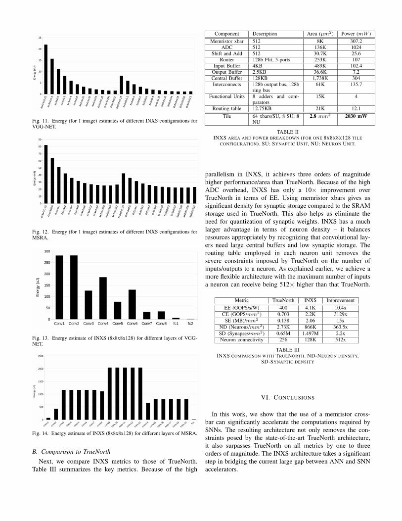
Fig. 11. Energy (for 1 image) estimates of different INXS configurations forVGG-NET.
Fig. 12. Energy (for 1 image) estimates of different INXS configurations forMSRA.
Fig. 13. Energy estimate of INXS (8x8x8x128) for different layers of VGG-NET.
Fig. 14. Energy estimate of INXS (8x8x8x128) for different layers of MSRA.
B. Comparison to TrueNorthNext, we compare INXS metrics to those of TrueNorth.
Table III summarizes the key metrics. Because of the high
Component Description Area (µm2) Power (mW )Memristor xbar 512 8K 307.2
ADC 512 136K 1024Shift and Add 512 30.7K 25.6
Router 128b Flit, 5-ports 253K 107Input Buffer 4KB 489K 102.4
Output Buffer 2.5KB 36.6K 7.2Central Buffer 128KB 1,738K 304Interconnects 128b output bus, 128b
ring bus61K 135.7
Functional Units 8 adders and com-parators
15K 4
Routing table 12.75KB 21K 12.1Tile 64 xbars/SU, 8 SU, 8
NU2.8 mm2 2030 mW
TABLE IIINXS AREA AND POWER BREAKDOWN (FOR ONE 8X8X8X128 TILE
CONFIGURATION). SU: SYNAPTIC UNIT, NU: NEURON UNIT.
parallelism in INXS, it achieves three orders of magnitudehigher performance/area than TrueNorth. Because of the highADC overhead, INXS has only a 10× improvement overTrueNorth in terms of EE. Using memristor xbars gives ussignificant density for synaptic storage compared to the SRAMstorage used in TrueNorth. This also helps us eliminate theneed for quantization of synaptic weights. INXS has a muchlarger advantage in terms of neuron density – it balancesresources appropriately by recognizing that convolutional lay-ers need large central buffers and low synaptic storage. Therouting table employed in each neuron unit removes thesevere constraints imposed by TrueNorth on the number ofinputs/outputs to a neuron. As explained earlier, we achieve amore flexible architecture with the maximum number of inputsa neuron can receive being 512× higher than that TrueNorth.
Metric TrueNorth INXS ImprovementEE (GOPS/s/W) 400 4.1K 10.4x
CE (GOPS/mm2) 0.703 2.2K 3129xSE (MB)/mm2 0.138 2.06 15x
ND (Neurons/mm2) 2.73K 866K 363.5xSD (Synapses/mm2) 0.65M 1.497M 2.2xNeuron connectivity 256 128K 512x
TABLE IIIINXS COMPARISON WITH TRUENORTH. ND-NEURON DENSITY,
SD-SYNAPTIC DENSITY
VI. CONCLUSIONS
In this work, we show that the use of a memristor cross-bar can significantly accelerate the computations required bySNNs. The resulting architecture not only removes the con-straints posed by the state-of-the-art TrueNorth architecture,it also surpasses TrueNorth on all metrics by one to threeorders of magnitude. The INXS architecture takes a significantstep in bridging the current large gap between ANN and SNNaccelerators.
REFERENCES
[1] K. Ahmed, A. Shrestha, Q. Qiu, and Q. Wu, “Probabilistic Inference Us-ing Stochastic Spiking Neural Networks on a Neurosynaptic Processor,”in Proceedings of IJCNN, 2015.
[2] F. Akopyan, J. Sawada, A. Cassidy, R. Alvarez-Icaza, J. Arthur,P. Merolla, N. Imam, Y. Nakamura, P. Datta, G. Nam, B. Taba,M. Beakes, B. Brezzo, J. Kuang, R. Manohar, W. Risk, B. Jackson, andD. Modha, “TrueNorth: Design and Tool Flow of a 65mW 1 MillionNeuron Programmable Neurosynaptic Chip,” IEEE Trans. on Computer-Aided Design of Integrated Circuits and Systems, vol. 34(10), 2015.
[3] J. Albericio, P. Judd, T. Hetherington, T. Aamodt, N. Jerger, andA. Moshovos, “Cnvlutin: Zero-Neuron-Free Deep Convolutional NeuralNetwork Computing,” in Proceedings of ISCA-43, 2016.
[4] B. Benjamin, P. Gao, E. McQuinn, S. Choudhary, A. Chandrasekaran,J. Bussat, R. Alvarez-Icaza, J. Arthur, P. Merolla, and K. Boahen,“Neurogrid: A Mixed-Analog-Digital Multichip System for Large-ScaleNeural Simulations,” Proceedings of the IEEE, vol. 102(5), 2014.
[5] Y. Cao, Y. Chen, and D. Khosla, “Spiking Deep Convolutional NeuralNetworks for Energy-Efficient Object Recognition,” International Jour-nal of Computer Vision, vol. 113(1), 2015.
[6] T. Chen, Z. Du, N. Sun, J. Wang, C. Wu, Y. Chen, and O. Temam, “Di-anNao: A Small-Footprint High-Throughput Accelerator for UbiquitousMachine-Learning,” in Proceedings of ASPLOS, 2014.
[7] Y.-H. Chen, J. Emer, and V. Sze, “Eyeriss: A Spatial Architecturefor Energy-Efficient Dataflow for Convolutional Neural Networks,” inProceedings of ISCA-43, 2016.
[8] Y. Chen, T. Luo, S. Liu, S. Zhang, L. He, J. Wang, L. Li, T. Chen, Z. Xu,N. Sun et al., “DaDianNao: A Machine-Learning Supercomputer,” inProceedings of MICRO-47, 2014.
[9] P. Chi, S. Li, Z. Qi, P. Gu, C. Xu, T. Zhang, J. Zhao, Y. Liu, Y. Wang,and Y. Xie, “PRIME: A Novel Processing-In-Memory Architecturefor Neural Network Computation in ReRAM-based Main Memory,” inProceedings of ISCA-43, 2016.
[10] D. Ciresan, U. Meier, and J. Schmidhuber, “Multi-Column Deep NeuralNetworks for Image Classification,” in Proceedings of CVPR, 2012.
[11] C.Yakopcic, M.Z.Alom, and T.M.Taha, “Memristor Crossbar Deep Net-work Implementation Based on a Convolutional Neural Network,” inProceedings of IJCNN, 2016.
[12] P. Diehl, D. Neil, J. Binas, M. Cook, S. Liu, and M. Pfeiffer, “Fast-Classifying, High-Accuracy Spiking Deep Networks Through Weightand Threshold Balancing,” in Proceedings of IJCNN, 2015.
[13] Z. Du, D. Rubin, Y. Chen, L. He, T. Chen, L. Zhang, C. Wu,and O. Temam, “Neuromorphic Accelerators: A Comparison BetweenNeuroscience and Machine-Learning Approaches,” in Proceedings ofMICRO-48, 2015.
[14] S. Esser, R. Appuswamy, P. Merolla, J. Arthur, and D. Modha,“Backpropagation for Energy-Efficient Neuromorphic Computing,” inProceedings of NIPS, 2015.
[15] S. Esser, P. Meroll, J.V.Arthur, A.S.Cassidy, R.Appuswamy, A. An-dreopoulos, D. Berg, J. McKinstry, T.Melano, D. Barch, C. Nolfo,P. Datta, A. Amir, B. Taba, M. Flickner, and D. Modha, “Convolu-tional Networks for Fast, Energy-Efficient Neuromorphic Computing,”in arXiv, 2016.
[16] D. Feldman, “The Spike Timing Dependence of Plasticity,” Neuron, no.75(4), 2012.
[17] B. Graham, “Fractional Max-Pooling,” arXiv preprint arXiv:1412.6071,2014.
[18] R. Hameed, W. Qadeer, M. Wachs, O. Azizi, A. Solomatnikov, B. Lee,S. Richardson, C. Kozyrakis, and M. Horowitz, “Understanding Sourcesof Inefficiency in General-Purpose Chips,” in Proceedings of ISCA,2010.
[19] K. He, X. Zhang, S. Ren, and J. Sun, “Delving Deep into Rectifiers:Surpassing Human-Level Performance on ImageNet Classification,”arXiv preprint arXiv:1502.01852, 2015.
[20] A. Hodgkin and A. Huxley, “A Quantitative Description of MembraneCurrent and its Application to Conduction and Excitation in Nerve,”Journal of Physiology, no. 117(4), 1952.
[21] E. Hunsberger and C. Eliasmith, “Spiking Deep Networks with LIFNeurons,” 2015, arXiv preprint 1510.08829.
[22] ——, “Training Spiking Deep Networks for Neuromorphic Hardware,”in arXiv preprint arXiv:1611.05141, 2016.
[23] A. Joubert, B. Belhadj, O. Temam, and R. Heliot, “Hardware SpikingNeurons Design: Analog or Digital?” in Proceedings of IJCNN, 2012.
[24] A. Kahng, B. Li, L.-S. Peh, and K. Samadi, “ORION 2.0: A Fast andAccurate NoC Power and Area Model for Early-Stage Design SpaceExploration,” in Proceedings of DATE, 2009.
[25] M. M. Khan, D. R. Lester, L. A. Plana, A. Rast, X. Jin, E. Painkras, andS. B. Furber, “SpiNNaker: Mapping Neural Networks onto a Massively-Parallel Chip Multiprocessor,” in Proceedings of IJCNN, 2008.
[26] A. Krizhevsky, I. Sutskever, and G. E. Hinton, “ImageNet Classificationwith Deep Convolutional Neural Networks,” in Proceedings of NIPS,2012.
[27] L. Kull, T. Toifl, M. Schmatz, P. A. Francese, C. Menolfi, M. Brandli,M. Kossel, T. Morf, T. M. Andersen, and Y. Leblebici, “A 3.1 mW8b 1.2 GS/s Single-Channel Asynchronous SAR ADC with AlternateComparators for Enhanced Speed in 32 nm Digital SOI CMOS,” Journalof Solid-State Circuits, 2013.
[28] B. Liu, Y. Chen, B. Wysocki, and T. Huang, “Reconfigurable Neuro-morphic Computing System with Memristor-Based Synapse Design,”Neural Processing Letters, no. 41(2), 2015.
[29] C. Liu, B. Yan, C. Yang, L. Song, Z. Li, and B. Liu, “A SpikingNeuromorphic Design with Resistive Crossbar,” in Proceedings of DAC,2015.
[30] W. McCulloch and W. Pitts, “A Logical Calculus of the Ideas Immanentin Nervous Activity,” Bulletin of Mathematical Biophysics, no. 5, 1943.
[31] E. Menendez, D. Maduike, R. Garg, and S. Khatri, “CMOS Comparatorsfor high-Speed and Low-Power Applications,” in Proceedings of ICCD,2006.
[32] P. Merolla, J. Arthur, R. Alvarez-Icaza, A. Cassidy, J. Sawada,F. Akopyan, B. Jackson, N. Imam, C. Guo, Y. Nakamura, B. Brezzo,I. Vo, S. Esser, R. Appuswamy, B. Taba, A. Amir, M. Flickner, W. Risk,R. Manohar, and D. Modha, “A Million Spiking-Neuron IntegratedCircuit with a Scalable Communication Network and Interface,” Science,vol 345, no. 6197, 2014.
[33] N. Muralimanohar et al., “CACTI 6.0: A Tool to Understand LargeCaches,” University of Utah, Tech. Rep., 2007.
[34] A. Nere, A. Hashmi, M. Lipasti, and G. Tononi, “Bridging the SemanticGap: Emulating Biological Neuronal Behaviors with Simple DigitalNeurons,” in Proceedings of HPCA-19, 2013.
[35] B. Reagen, P. Whatmough, R. Adolf, S. Rama, H. Lee, S. Lee, J. M.Hernandez, Lobato, G.-Y. Wei, and D. Brooks, “Minerva: EnablingLow-Power, High-Accuracy Deep Neural Network Accelerators,” inProceedings of ISCA-43, 2016.
[36] J. Seo, B. Brezzo, Y. Liu, B. Parker, S. Esser, R. Montoye, B. Rajendran,J. Tierno, L. Chang, D. Modha, and D. Friedman, “A 45nm CMOS Neu-romorphic Chip with a Scalable Architecture for Learning in Networksof Spiking Neurons,” in Proceedings of CICC, 2011.
[37] A. Shafiee, A. Nag, N. Muralimanohar, R. Balasubramonian, J. Strachan,M. Hu, R. Williams, and V. Srikumar, “ISAAC: A Convolutional NeuralNetwork Accelerator with In-Situ Analog Arithmetic in Crossbars,” inProceedings of ISCA, 2016.
[38] S.Han, X. Liu, H. Mao, J. Pu, A. Pedram, M. Horowitz, and W. Dally,“EIE: Efficient Inference Engine on Compressed Deep Neural Network,”in Proceedings of ISCA, 2016.
[39] K. Simonyan and A. Zisserman, “Very Deep Convolutional Networksfor Large-Scale Image Recognition,” arXiv preprint arXiv:1409.1556,2014.
[40] T. Taha, R. Hasan, C. Yakopcic, and M. McLean, “Exploring the DesignSpace of Specialized Multicore Neural Processors,” in Proceedings ofIJCNN, 2013.
[41] M. Talsania and E. John, “A Comparative Analysis of Parallel PrefixAdders,” in Proceedings of the International Conference on ComputerDesign (CDES), 2013.
[42] T. Tang, L. Xia, B. Li, R. Luo, Y. Chen, Y. Wang, and H. Yang,“Spiking Neural Network with RRAM: Can We Use It for Real-WorldApplication?” in Proceedings of DATE, 2015.
[43] C. Yakopcic and T. M. Taha, “Energy Efficient Perceptron PatternRecognition using Segmented Memristor Crossbar Arrays,” in Proceed-ings of IJCNN, 2013.