Embed Size (px)
Citation preview
Seminar Report
IP Reuse Methodology in Industrial Practice
Student: Kailai Sun Mentor: Prof. Radetzki
Institut für Technische Informatik
University of Stuttgart
Summer Semester 06
Page 1 of 22
Seminar Report
Abstract
With widespread recent stress on System-On-Chip (SOC), intellectual property (IP) reuse based system design is becoming recently an industrial standard. The publishing of the Reuse Methodology Manual (RMM) that defines the various stages for IP Reuse and SOC design will provide the IC engineers some precious advice and experience in both planning and designing phases. In this report, I will propose some essential issues in IP reuse design, including current design challenges, primary design methodology and inevitable test/verification, which is significantly necessary for success of the design in practice. Finally I will identify some obstacles that must be overcome, manly in RTL coding phase.
Key words: IP, Reuse methodology, SOC, RTL
Page 2 of 22
Seminar Report
Contents
Abstract..........................................................................2
Contents..........................................................................3
1 Preface.......................................................................4
1.1 Introduction..........................................................4 1.1.1 Application Background............................................4 1.1.2 What’s IP?.......................................................4
1.2 Why IP Reuse in System-on-Chip (SoC)..................................4 1.3 Current challenges in practice........................................5
2 Basic Analysis of Reuse Methodology...........................................6
2.1 Reuse Methodology.....................................................6 2.2 SOC design based on IP Reuse..........................................7 2.3 How to create a reusable macro........................................8 2.4 SOC integration with reuse IPs.......................................11 2.5 SOC verification.....................................................13 2.6 Documentation........................................................15
3 Some Guidelines and Rules in RTL Coding......................................16
3.1 Coding for Clocks and Resets.........................................16 3.1.1 Clocks...........................................................16 3.1.2 Resets...........................................................17
3.2 Coding for Synthesis.................................................18 3.2.1 Registers and latches............................................18 3.2.2 Sensitivity Lists................................................18 3.2.3 Coding State Machines............................................18
3.3 Partitioning for Synthesis...........................................19 3.3.1 Register all outputs.............................................19 3.3.2 Some remarks in the partitioning.................................19
4 Conclusion...................................................................21
5 Reference....................................................................22
Page 3 of 22
Seminar Report
1 Preface
1.1 Introduction
1.1.1 Application Background
The term “design reuse” is now quite popular in the fast-paced, time-to-market driven
industry. Products must be designed, tested, and manufactured faster than ever to meet a
technology-driven market bent on having the latest technology. Engineers have realized that
reusing existing blocks of intellectual property (IP) from previous designs is one of the shortcuts
to get ahead on the project timeline.
Today, almost all the large IC companies with tremendous talent and capital resource are
competing in research and development for this cutting-edge technology.
1.1.2 What’s IP?
Nowadays more and more papers and books have been written about reuse designs. Most of
the publications name the design intellectual property or IP for short. But what really makes up the
IP? The common answer prevalent in the IC design world is that the RTL description of the design
is IP. To a patent lawyer that may be so, but conceptually speaking, the RTL description is only
half of the total IP design. What helps describe the workings and functionality of the design
through a process of testing/validating is in fact the other half of the IP design. A set of functional
tests that validate the design is as important as the design itself. It is self-evident that the test and
verification processes are taking around 70% of workload during the complete design today. [3]
1.2 Why IP Reuse in System-on-Chip (SoC)
With the development of the larger and larger, more and more complicated SoC design, a number of design methodologies have been researched and developed to help improve our capability to solve the increasing design problems.
From 1990s, the design technique based on HDL descriptions and EDA software (design, simulation, synthesis, verification and so on) from an abstraction level RTL has played an important role in VLSI design, especially in ASIC design methodology. In spite of all the attractive features of this methodology, the increasing complexity of new SoCs makes it very difficult for design teams of industry to design these components all by themselves. A typical SoC nowadays involves processor (CPU, MCU, MPU), ASAP, all kinds of digital IP (voice/video signal processing, communication), analog and RF components (transceiver, antenna). Normally, industry requires designing all these IPs under one platform or even within the same company, concurrently with the ever increasing time-to-market pressure. This naturally leads to the IP-Reuse techniques. [4]
Page 4 of 22
Seminar Report
Design Reuse is defined as follows: "The ability to retarget previously designed building
blocks or cores on a chip for a new design in order to reduce time to market" [1], “IP-Reuse methodology has been introduced to cope with very large and complex designs. It basically involves partitioning of the designs into smaller IP blocks with well-defined functionality that can be re-used across multiple designs.”[5]
IP reuse shows advantages in the following aspects: (1) Time-to-Market: Pre-designed blocks are used in the design, so the design time has been much shorter. (2) Costs: Reusability strategy decreases the overhead resulting from the repeating design. (3) Performance: IP providers can always provide these IPs with optimized algorithms. (4) Hardware Area: Optimized designs will take relatively less area of the chip.
1.3 Current challenges in practice
The ordinary challenges in practice of IP based SoC design is as follows: (1) Power: Low power design is now a popular research emphasis, for with the more and more complicated system chip, more and more IPs are integrated in one chip. (2) Process integration: SoC does the system function, instead of individual function. How to integrate individual processes is always a tough problem. (3) Quality of products: Chip’s performance, area and power are all key factors to market success. (4) Verification: Increasing chip complexity makes it more difficult. (5) SoC design includes embedded processor cores and thus a significant software component, which leads to additional methodology, processor, and organizational challenges. (Not presented here)
Page 5 of 22
Seminar Report
2 Basic Analysis of Reuse Methodology
2.1 Reuse Methodology
Definitions: IP (or core, block, or Macro), terms interchangeably. Table1 compares some
properties between soft cores and Hard cores. In practice, we need to select our cores according to
the design requirements.
There are mainly two cores in SoC design, Soft core and hard core.
Soft core is shipped as Synthesizable RTL code which allows items to be added and cores to
be re-synthesized. It resembles a white box and the implementation is visible and modifiable, but
is not very predictable in terms of performance, therefore relatively high effort need to be taken to
embed it into a design.
As to hard core, it resembles a black box and items can not be re-synthesized, because it is
fully designed, placed, routed by the supplier and provided as GDSII file. Final design must be
fabricated using the specified silicon process, but it’s relatively simple to implement it in to a
design.
As far as the patent security is concerned, hard core takes positively priority. “Black Box” successfully prevents from unauthorized copy.
Soft cores Hard cores
Models Synthesizable behavioral Layout + data sheet
Portability Yes No
Design time Higher Lower
Optimization Low High
Timing issues Full timing verification after
synthesis
Timing characteristics
provided; to be trusted.
Table1. Soft/hard cores
Page 6 of 22
Seminar Report
2.2 SOC design based on IP Reuse
Figure1. Typical Structure of Microprocessor based SoC [5]
Normally, SoC consists of the following blocks: Microcontroller, microprocessor or DSP cores. ARM is now the most popular microprocessor
in SoC and embedded system design, fig.1 is a typical example of ARM application. Standard interface cores including industry standards such as UART, PCI, USB, FireWire,
Ethernet, I2C and SPI. Memory cores including a selection of D-cache, I-cache, ROM, RAM, Flash and EEPROM. Peripherals including cache controllers, counter-timers, DMA controllers, real-time timers
and power-on reset generators Timing sources including oscillators and phase-locked loops (PLL) Digital cores including JPEG compressor, MPEG decoder, VGA. Analog cores including clock recovery, RF components, ADCs and DACs Voltage regulators and power management circuits
These blocks can be connected by standard bus such as the AMBA (Advanced Micro-controller Bus Architecture) bus from ARM. DMA controllers can transfer data directly
Page 7 of 22
Seminar Report
between memory and external interfaces, by-passing the processor core and thereby increasing the data throughput and raise the speed of the SoC. Fig1[5] shows a typical structure of microprocessor based SoC which contains most of the blocks mentioned above.
Under IP Reuse platform, design efficiency is achieved by ease of plug-and-play. In this way, System-on-Chip takes the place of Chips-on-Board in industrial practice.
2.3 How to create a reusable macro
First common rule: “Before a macro can been reusable, it has to be usable” [7]. This means a
robust and correct design is by all means the prerequisite. Engineers have tried to find all kinds of
measure to make design perfect, such as good coding style, well-specified and independent
testbenches and ready-made test toolkits.
To design a fully usable macro, the following rules have to be taken into account:
Portability under multi-technologies: For soft cores, this means the synthesis results
consistent on multiple libraries. For hard cores, this means a satisfactory result after
mapping the core into arbitrary new technology.
Portability under multi-simulators: A reusable core means it can work under different
major commercial simulators and emulators, not merely the original one. It should be as
generic as possible.
A high level of confidence of the design: A rigorous test and verification is absolutely
indispensable, as well as the rapid-prototype which can do the test in practical system.
Complete documentation of high quality: Accessible and valid parameters, configuration
values have to be documented with thorough commenting, as well as special values on
any restrictions.
Normally, any SOC design starts from writing the specifications, during which some key
decisions have to be made before selection or design of the reusable IPs for our chip: [5]
(1) Functional Design which consists of two facets. One is busing scheme specification and
here Transaction Level Modeling (TLM) with SystemC is recommended which is now
practical in industry. Another one is that debug methods and processes for hardware and
software must be planned.
(2) Timing and Synthesis. Reset strategy for the chip must be considered carefully and
synchronous reset is recommended (Discussed later in chapter 3). Besides, timing, area
and power issues must be taken into account in synthesis strategy. Each macro must have
its independent synthesis scripts.
(3) Physical Design. Floorplanning strategy should be well defined if you plan to mix hard
Page 8 of 22
Seminar Report
and soft macros in one chip and it should be specified as early as possible in design, for it
is the key point in the interface strategy and therefore in the integration process as well.
(4) Verification Strategy. Verification ensures that Design Under Verification (DUV) works
for a specification and it proves absence of bugs.
(5) Test Strategy: Testing checks if the DUV works for the specified test cases and it proves
presence of bugs.
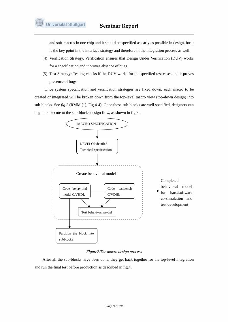
Once system specification and verification strategies are fixed down, each macro to be
created or integrated will be broken down from the top-level macro view (top-down design) into
sub-blocks. See fig.2 (RMM [1], Fig.4-4). Once these sub-blocks are well specified, designers can
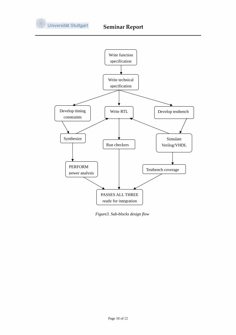
begin to execute to the sub-blocks design flow, as shown in fig.3.
MACRO SPECIFICATION
DEVELOP detailed
Technical specification
Create behavioral model
Code behavioral
model C/VHDL
Code testbench
C/VDHL
Test behavioral model
Completed behavioral model for hard/software co-simulation and test development
Partition the block into
subblocks
Figure2.The macro design process
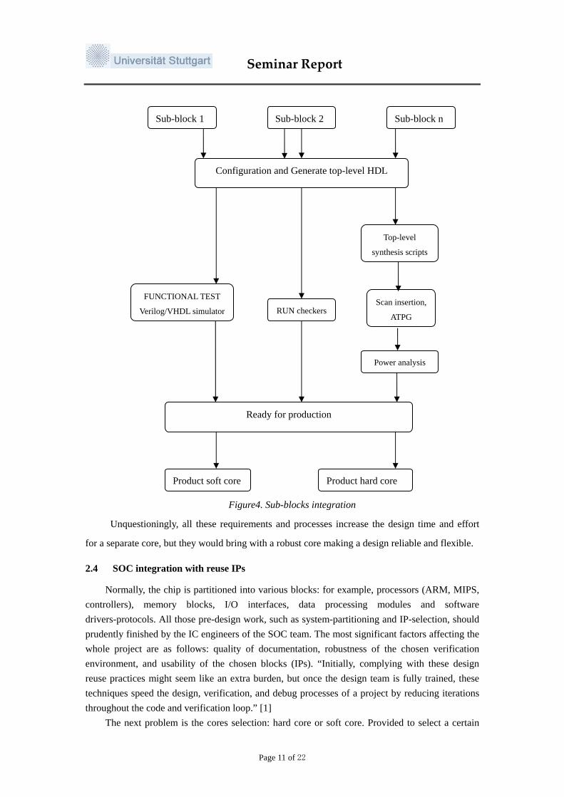
After all the sub-blocks have been done, they get back together for the top-level integration
and run the final test before production as described in fig.4.
Page 9 of 22
Seminar Report
Figure3. Sub-blocks design flow
Develop testbench
Write technical specification
Develop timing constraints
Synthesize Run checkers
Write RTL
Simulate Verilog/VHDL
PERFORM power analysis
Testbench coverage
PASSES ALL THREE ready for integration
Write function specification
Page 10 of 22
Seminar Report
Sub-block 1 Sub-block 2 Sub-block n
Configuration and Generate top-level HDL
Top-level
synthesis scripts
FUNCTIONAL TEST
Verilog/VHDL simulator RUN checkers
Power analysis
Ready for production
Figure4. Sub-blocks integration
Unquestioningly, all these requirements and processes increase the design time and effort
for a separate core, but they would bring with a robust core making a design reliable and flexible.
Scan insertion,
ATPG
Product soft core Product hard core
2.4 SOC integration with reuse IPs
Normally, the chip is partitioned into various blocks: for example, processors (ARM, MIPS, controllers), memory blocks, I/O interfaces, data processing modules and software drivers-protocols. All those pre-design work, such as system-partitioning and IP-selection, should prudently finished by the IC engineers of the SOC team. The most significant factors affecting the whole project are as follows: quality of documentation, robustness of the chosen verification environment, and usability of the chosen blocks (IPs). “Initially, complying with these design reuse practices might seem like an extra burden, but once the design team is fully trained, these techniques speed the design, verification, and debug processes of a project by reducing iterations throughout the code and verification loop.” [1]
The next problem is the cores selection: hard core or soft core. Provided to select a certain
Page 11 of 22
Seminar Report
core for a specific application and the module library provides both hard and soft cores. It is economic and advisable to select the hard macros if these hard ones totally and precisely match the presented requirements. However, if a new technology is retargeted and a tiny change is required, thus the advantage of RTL design (soft core) will allow doing corresponding modification.
In practice, there are some modules, which benefit the design much, be used as hard cores. A microprocessor hard core, for example, has no timing troubles which can not be simply and completely automated. Therefore, if the technology and other parameters of the processor are given, it is efficient to provide this core in hard form. But for other cores, soft approach is comparatively an advisable choice owing to its flexibility and the increasing effectiveness of EDA. On the other hand, the design attaching importance to back end automation will find more time and resource available in efficiency than the front end work.
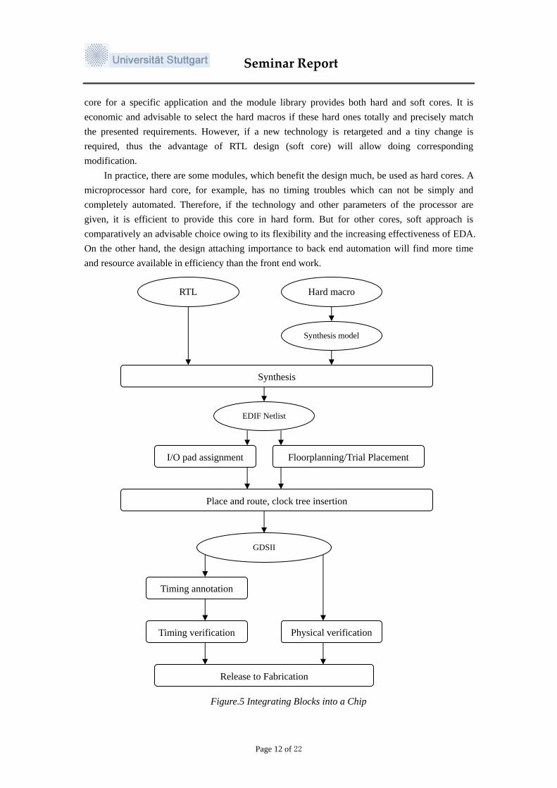
RTL Hard macro
Synthesis model
Figure.5 Integrating Blocks into a Chip
Synthesis
EDIF Netlist
I/O pad assignment Floorplanning/Trial Placement
Place and route, clock tree insertion
GDSII
Timing annotation
Physical verification Timing verification
Release to Fabrication
Page 12 of 22
Seminar Report
If the blocks have been c use, then the integration
proc
on, engineers have to consider interface design problem, which focuses on the matc
usable blocks in SoC. ore storage is needed
and
T ess of SOC is being attached great importance in industrial practice and now
y employed approach to verification process is as follows: first inclu
erified blocks in it. Veri
especially at the e
verification com
reated and documented for easiness to ess is relatively straightforward. Otherwise, then integration of these macros will be a
nightmare. In additihing of interface bit-number, voltage, current and other parameters among these blocks.
Verification process (with details next) and interface design may complicate the integration process and increase design overhead considerably.
Fig.5 gives the overview of integrating various reBesides, with the development of application requirement, more and mtakes now even more than 50% of the overall silicon area of one SoC. Thereby the objective
of the work for the engineers will be making the memories as small and fast as possible, concurrently with the minimum power.
2.5 SOC verification
he verification proc an integral part of the SOC design process. The comprehensive verification process would
depend primarily on the following factors: the quality of the test schemes, testbench models, robustness of reusable chosen IPs and the verification/validation flow. Essentially, as to the execution of the test plans, the prerequisite is to check that all embedded IPs have been thoroughly verified and are indeed reusable.
Nowadays the most frequentlde and interconnect all blocks in the testbench, then run the testbench at the top-level and at
the same time activate all the blocks. Observing transaction activity at primary I/O and memory contents would allow us to state whether the chip is working correctly or not.
We can take the advantage of the fact that the SoC has IPs and pre-vfication always starts from the specifications: the design specs and the test plans. The goal for
the verification engineers is to create a full verification system as fast as possible. A useful guideline is to define the verification based on high-level transaction,nd-to-end transactions. End-to-end transactions mean considering problems at system-level
instead of the internal details. Take an example of a packet router, packets can be transferred via 8-bit interface. In this case, the test scenarios should be defined to end-to-end packets, not in terms of sequences of 8-bit vectors. This kind of scenario seems to “look at the big picture,”
One method that can easily realize the full SoC verification is using unit ponents. Normally, it should be straightforward to use them. Checkers of IP properties can be
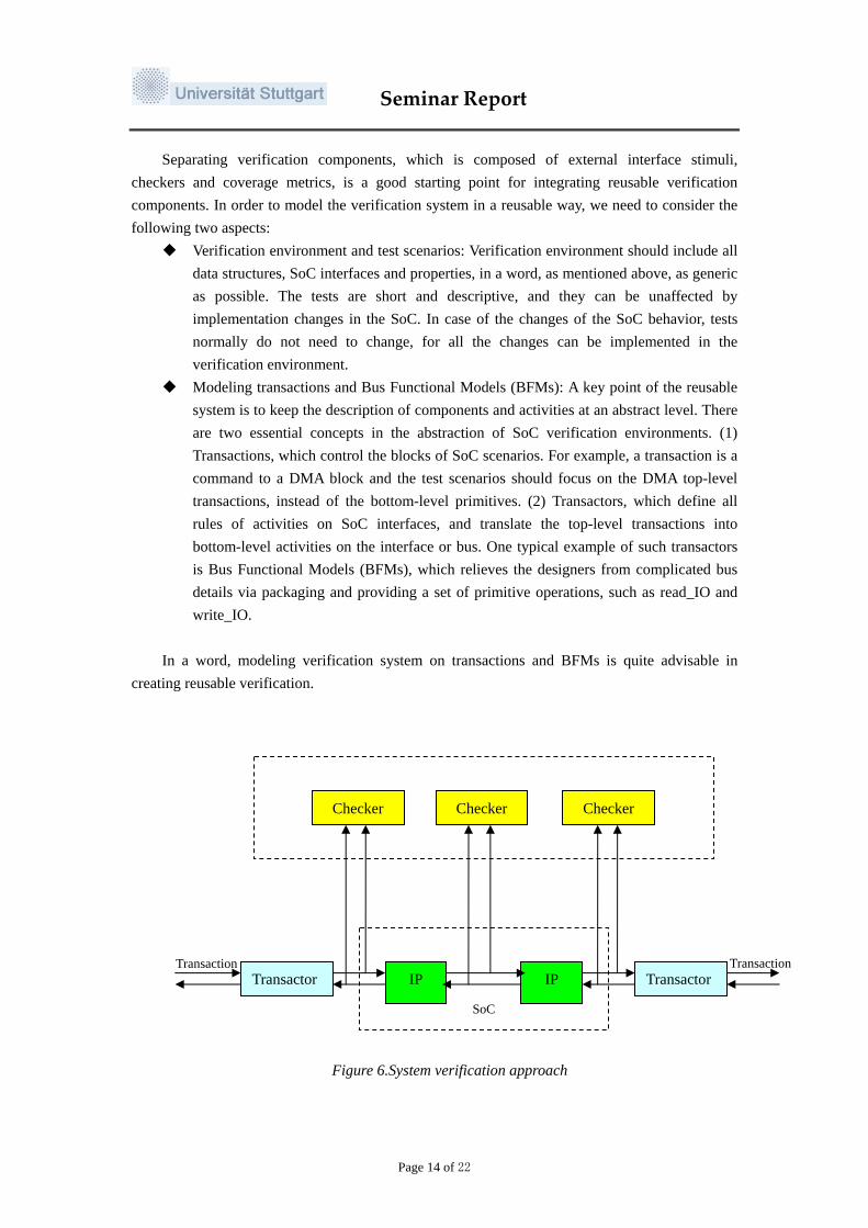
integrated into the SoC verification system. For example, these checkers can check that all the transitions in Finite State Machine (FSM) are correct. Other verification components may be reused, given that the IP verification is planned correctly. As these IPs are integrated into SoC, many of the IP interfaces become internal interfaces between adjacent blocks, thereof there is no need to drive their inputs any longer. Figure 6 presents this procedure. If test generators for remaining external interfaces are flexible, configurable and independent, then the system-stimuli could be taken as is from various testing environments. Actually it is not difficult to create such generic test generators.
Page 13 of 22
Seminar Report
Transaction
Separating verification components, which is composed of external interface stimuli, chec
ironment and test scenarios: Verification environment should include all
nctional Models (BFMs): A key point of the reusable
a word, modeling verification system on transactions and BFMs is quite advisable in
creat
Figure 6.System verification approach
kers and coverage metrics, is a good starting point for integrating reusable verification components. In order to model the verification system in a reusable way, we need to consider the following two aspects:
Verification envdata structures, SoC interfaces and properties, in a word, as mentioned above, as generic as possible. The tests are short and descriptive, and they can be unaffected by implementation changes in the SoC. In case of the changes of the SoC behavior, tests normally do not need to change, for all the changes can be implemented in the verification environment. Modeling transactions and Bus Fusystem is to keep the description of components and activities at an abstract level. There are two essential concepts in the abstraction of SoC verification environments. (1) Transactions, which control the blocks of SoC scenarios. For example, a transaction is a command to a DMA block and the test scenarios should focus on the DMA top-level transactions, instead of the bottom-level primitives. (2) Transactors, which define all rules of activities on SoC interfaces, and translate the top-level transactions into bottom-level activities on the interface or bus. One typical example of such transactors is Bus Functional Models (BFMs), which relieves the designers from complicated bus details via packaging and providing a set of primitive operations, such as read_IO and write_IO.
Ining reusable verification.
Transaction Transactor Transactor IP IP
Checker Checker Checker
SoC
Page 14 of 22
Seminar Report
Besides, for SoC verification, a great amount of efforts are being paid to deal with the
embe
D undoubtedly more and more important in SOC design, particularly for
IP-re
dded memory verification at behavioral level, which is an important and necessary step to reusability as well. Visualizing the behavior of embedded memories as FSM (finite state machine) is a very innovative idea. Check details in [5]
2.6 Documentation
ocumentation is
use design. A SOC design will include even over 10 million gates and during the design, lots
of questions, for example IP selection and IP integration, would be solved based on the existing
documentation. The accuracy of the documentation takes the same place as the quality of the HDL
code. System architecture, function description, detailed description of I/O, dataflow diagram,
design dependency/restrictions and test patterns should be separately documented clearly, as well
as the installation wizard, README files and other application notes.[5]
Page 15 of 22
Seminar Report
3 Some Guidelines and Rules in RTL Coding
3.1 Coding for Clocks and Resets
3.1.1 Clocks
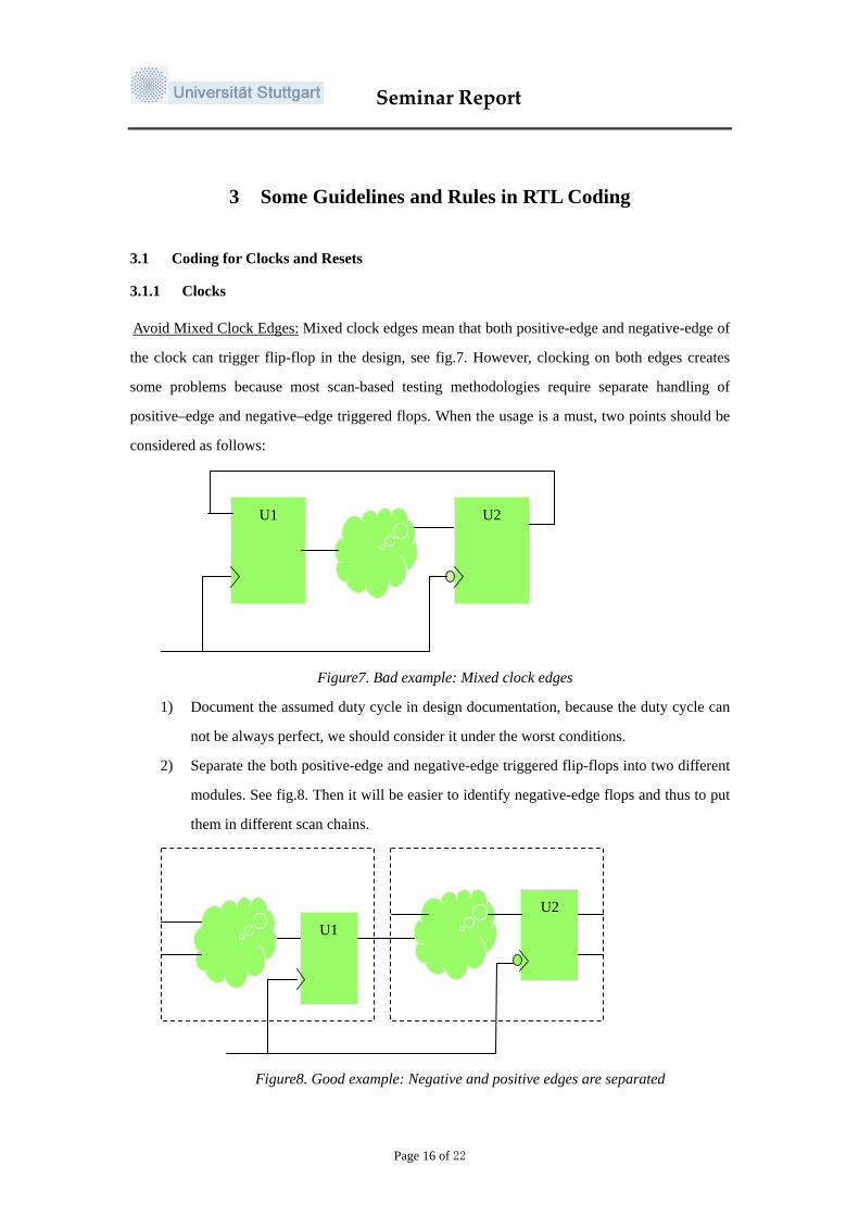
Avoid Mixed Clock Edges: Mixed clock edges mean that both positive-edge and negative-edge of
the clock can trigger flip-flop in the design, see fig.7. However, clocking on both edges creates
some problems because most scan-based testing methodologies require separate handling of
positive–edge and negative–edge triggered flops. When the usage is a must, two points should be
considered as follows:
Figure7. Bad example: Mixed clock edges
U1 U2
1) Document the assumed duty cycle in design documentation, because the duty cycle can
not be always perfect, we should consider it under the worst conditions.
2) Separate the both positive-edge and negative-edge triggered flip-flops into two different
modules. See fig.8. Then it will be easier to identify negative-edge flops and thus to put
them in different scan chains.
U2
U1
Figure8. Good example: Negative and positive edges are separated
Page 16 of 22
Seminar Report
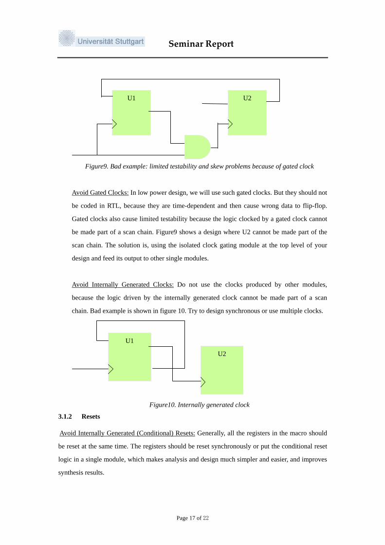
f gaFigure9. Bad example: limited testability and skew problems because o ted clock
void Gated Clocks:A
U1 U2
In low power design, we will use such gated clocks. But they should not
void Internally Generated Clocks:
be coded in RTL, because they are time-dependent and then cause wrong data to flip-flop.
Gated clocks also cause limited testability because the logic clocked by a gated clock cannot
be made part of a scan chain. Figure9 shows a design where U2 cannot be made part of the
scan chain. The solution is, using the isolated clock gating module at the top level of your
design and feed its output to other single modules.
A Do not use the clocks produced by other modules,
3.1.2 Resets
Avoi ernally Generated (Conditional) Resets:
because the logic driven by the internally generated clock cannot be made part of a scan
chain. Bad example is shown in figure 10. Try to design synchronous or use multiple clocks.
Figure10. Internally generated clo
U2
U1
ck
d Int Generally, all the registers in the macro should
be reset at the same time. The registers should be reset synchronously or put the conditional reset
logic in a single module, which makes analysis and design much simpler and easier, and improves
synthesis results.
Page 17 of 22
Seminar Report
3.2 Coding for Synthesis
3.2.1 Registers and latches
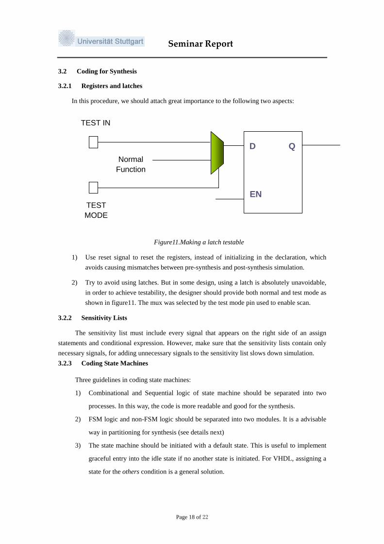
In this procedure, we should attach great importance to the following two aspects:
Figure11.Making a latch testable
TEST IN
1) Use reset signal to reset the registers, instead of initializing in the declaration, which avoids causing mismatches between pre-synthesis and post-synthesis simulation.
2) Try to avoid using latches. But in some design, using a latch is absolutely unavoidable, in order to achieve testability, the designer should provide both normal and test mode as shown in figure11. The mux was selected by the test mode pin used to enable scan.
3.2.2 Sensitivity Lists
The sensitivity list must include every signal that appears on the right side of an assign statements and conditional expression. However, make sure that the sensitivity lists contain only necessary signals, for adding unnecessary signals to the sensitivity list slows down simulation. 3.2.3 Coding State Machines
Three guidelines in coding state machines:
1) Combinational and Sequential logic of state machine should be separated into two
processes. In this way, the code is more readable and good for the synthesis.
2) FSM logic and non-FSM logic should be separated into two modules. It is a advisable
way in partitioning for synthesis (see details next)
3) The state machine should be initiated with a default state. This is useful to implement
graceful entry into the idle state if no another state is initiated. For VHDL, assigning a
state for the others condition is a general solution.
D Q
EN
Normal
Function
TEST MODE
Page 18 of 22
Seminar Report
3.3 Partitioning for Synthesis
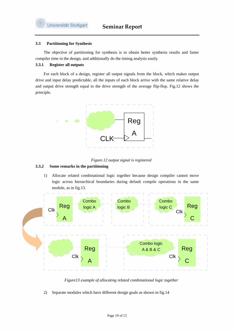
The objective of partitioning for synthesis is to obtain better synthesis results and faster compiler time in the design, and additionally do the timing analysis easily. 3.3.1 Register all outputs
For each block of a design, register all output signals from the block, which makes output drive and input delay predictable, all the inputs of each block arrive with the same relative delay and output drive strength equal to the drive strength of the average flip-flop. Fig.12 shows the principle.
Figure.12 output signal is registered 3.3.2 Some remarks in the partitioning
1) Allocate related combinational logic together because design compiler cannot move logic across hierarchical boundaries during default compile operations in the same module, as in fig.13.
Figure13 example of allocating related combinational logic together
2) Separate modules which have different design goals as shown in fig.14
Reg
A CLK
Combo logic A
Combo logic B
Combo logic C Reg Reg
Clk Clk A C
Clk Reg
A
Combo logic A & B & C Reg
Clk C
Page 19 of 22
Seminar Report
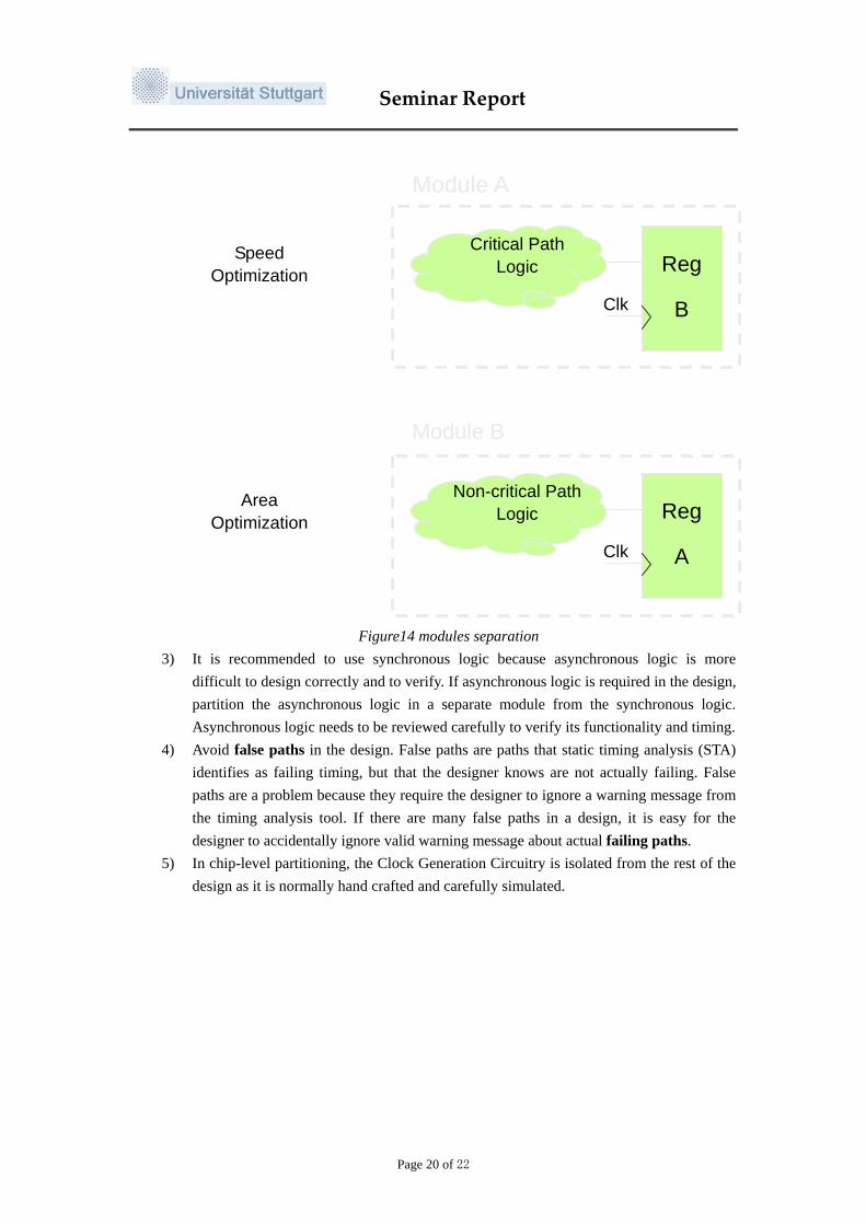
Module A
Figure14 modules separation
3) It is recommended to use synchronous logic because asynchronous logic is more difficult to design correctly and to verify. If asynchronous logic is required in the design, partition the asynchronous logic in a separate module from the synchronous logic. Asynchronous logic needs to be reviewed carefully to verify its functionality and timing.
4) Avoid false paths in the design. False paths are paths that static timing analysis (STA) identifies as failing timing, but that the designer knows are not actually failing. False paths are a problem because they require the designer to ignore a warning message from the timing analysis tool. If there are many false paths in a design, it is easy for the designer to accidentally ignore valid warning message about actual failing paths.
5) In chip-level partitioning, the Clock Generation Circuitry is isolated from the rest of the design as it is normally hand crafted and carefully simulated.
Clk
Reg
B
Logic Critical Path Speed
Optimization
Module B
Clk
Non-critical Path
Logic Area Reg Optimization
A
Page 20 of 22
Seminar Report
4 Conclusion
This report has presented the methodology and guidelines that will improve the reusability of
IP cores in industrial practice.
As a new design abstraction, IP reuse technology enables cost-efficient embedding of IP
module and provides flexibility in the application domain.
In order to maximize the reusability of IP blocks, elaborate design, rigorous validation and
complete documentation are essential in the SoC design. Reliably reusable IP blocks enable
successful SoC integration, and reduce time to the market.
SoC technology, based on IP reuse, is a fast-developing technology which has
unquestioningly a promising future.
Page 21 of 22
Seminar Report
5 Reference
[1] Michael Keating and Pierre Bricaud: “Reuse Methodology Manual for System-on-a-Chip
Designs”, Kluwer Academic Publishers, 1999.
[2] RK Gupta, Y Zorian: “Introducing core-based system design”, Design & Test of
Computers, IEEE, 1997
[3] Allen C.H.Wu: Business Trends and Design Methodologies for IP Reuse. Computer
Science Department, Tsing Hua University, Taiwan, 2002
[4] Daniel D.Gajski: Essential Issues for IP Reuse, Proceedings of the ASP-DAC, 2000
[5] Pierre J. Bricaud: IP Reuse Creation for System-on-a-Chip Design, Custom Integrated
Circuits, 1999
[6] Gregg D. Lahti: Test Benches: The Dark Side of IP Reuse, Synopsys Users Group, San
Jose, 2000
[7] IMEC Corporation: Design Reuse, http://www.imec.be/reuse, 2003
[8] Ramesh Chandra: IP-Reuse and Platform Base Designs, STMicroelectronics, Inc San
Diego, USA , http://www.us.design-reuse.com/articles/article6125.html, 2003
[9] Uwe Badelt, Martin Radetzki: sciPROVE: C++ Based Verification Environment for IP
and SoC Design, Forum on Design Language (FDL), 2003
[10] D. Geist, G. Biran, T. Arons, M. Slavkin, Y. Nustov, M.Farkas, K. Holtz, A. Long, D. King,
S. Barret: A Methodology For the Verification of a ‘System on Chip’, DAC, 1999.
Page 22 of 22