Embed Size (px)
Citation preview
Technical Support Line: 1-800-LATTICE or (408) 826-6002IDE-ISPML-RM 8.2.1
ispLSI Macro LibraryReference ManualVersion 8.2
ispLSI Macro Library Reference Manual 2
Copyright
This document may not, in whole or part, be copied, photocopied, reproduced,translated, or reduced to any electronic medium or machine-readable form withoutprior written consent from Lattice Semiconductor Corporation.
The software described in this manual is copyrighted and all rights are reserved byLattice Semiconductor Corporation. Information in this document is subject to changewithout notice.
The distribution and sale of this product is intended for the use of the originalpurchaser only and for use only on the computer system specified. Lawful users ofthis product are hereby licensed only to read the programs on the disks, cassettes, ortapes from their medium into the memory of a computer solely for the purpose ofexecuting them. Unauthorized copying, duplicating, selling, or otherwise distributingthis product is a violation of the law.
Trademarks
The following trademarks are recognized by Lattice Semiconductor Corporation:
Generic Array Logic, ISP, ispANALYZER, ispATE, ispCODE, ispDCD,ispDesignEXPERT, ispDOWNLOAD, ispDS, ispDS+, ispEXPERT, ispGDS, ispGDX,ispHDL, ispJTAG, ispSmartFlow, ispStarter, ispSTREAM, ispSVF, ispTA, ispTEST,ispTURBO, ispVECTOR, ispVerilog, ispVHDL, ispVM, Latch-Lock, LHDL, pDS+, RFT,and Twin GLB are trademarks of Lattice Semiconductor Corporation. E2CMOS, GAL,ispGAL, ispLSI, pDS, pLSI, Silicon Forest, and UltraMOS are registered trademarksof Lattice Semiconductor Corporation.
SPEEDSearch, Performance Analyst, and DesignDirect are trademarks of VantisCorporation. Kooldip, MACH, MACHPRO, MACHXL, Monolithic Memories, PAL,PALASM, and Vantis are registered trademarks of Vantis Corporation.
Project Navigator is a trademark of Data I/O Corporataion. ABEL-HDL is a registeredtrademark of Data I/O Corporation.
All other trademarks and registered trademarks are the property of their respectiveowners.
Lattice Semiconductor Corporation5555 NE Moore Ct.Hillsboro, OR 97124
(503) 268-8000
August 2000
Table of Contents
Preface . . . . . . . . . . . . . . . . . . . . . . . . . . . . . . . . . . . . . . . . . . . . . . . . . . . . . . . . . . . . . . . . . . . . 7Overview . . . . . . . . . . . . . . . . . . . . . . . . . . . . . . . . . . . . . . . . . . . . . . . . . . . . . . . . . . . . . . . . . . 7Purpose and Scope . . . . . . . . . . . . . . . . . . . . . . . . . . . . . . . . . . . . . . . . . . . . . . . . . . . . . . . . . . 8Documentation Conventions . . . . . . . . . . . . . . . . . . . . . . . . . . . . . . . . . . . . . . . . . . . . . . . . . . . 9
Signal Names . . . . . . . . . . . . . . . . . . . . . . . . . . . . . . . . . . . . . . . . . . . . . . . . . . . . . . . . . . . . 9Truth Tables . . . . . . . . . . . . . . . . . . . . . . . . . . . . . . . . . . . . . . . . . . . . . . . . . . . . . . . . . . . . 11Module Macro Truth Tables . . . . . . . . . . . . . . . . . . . . . . . . . . . . . . . . . . . . . . . . . . . . . . . . 12Pin Labeling . . . . . . . . . . . . . . . . . . . . . . . . . . . . . . . . . . . . . . . . . . . . . . . . . . . . . . . . . . . . 13Logic Resources. . . . . . . . . . . . . . . . . . . . . . . . . . . . . . . . . . . . . . . . . . . . . . . . . . . . . . . . . 14Using the NOMIN Attribute . . . . . . . . . . . . . . . . . . . . . . . . . . . . . . . . . . . . . . . . . . . . . . . . . 15
Quick Reference Macro Table . . . . . . . . . . . . . . . . . . . . . . . . . . . . . . . . . . . . . . . . . . . . . . . . 16
Arithmetic Functions . . . . . . . . . . . . . . . . . . . . . . . . . . . . . . . . . . . . . . . . . . . . . . . . . . . . . . 38Adders . . . . . . . . . . . . . . . . . . . . . . . . . . . . . . . . . . . . . . . . . . . . . . . . . . . . . . . . . . . . . . . . . . . . . 39
ADDF1, ADDF2, F3ADD, ADDF4, ADDF8, ADDF8A, and ADDF16A. . . . . . . . . . . . . . . . . . . 39ADDH1, ADDH2, ADDH3, ADDH4, ADDH8, ADDH8A, and ADDH16A . . . . . . . . . . . . . . . . . 54
Comparators . . . . . . . . . . . . . . . . . . . . . . . . . . . . . . . . . . . . . . . . . . . . . . . . . . . . . . . . . . . . . . . . . 67CMP2, CMP4, and CMP8 . . . . . . . . . . . . . . . . . . . . . . . . . . . . . . . . . . . . . . . . . . . . . . . . . . . . 67MAG2, MAG4, and MAG8 . . . . . . . . . . . . . . . . . . . . . . . . . . . . . . . . . . . . . . . . . . . . . . . . . . . 68
Multipliers . . . . . . . . . . . . . . . . . . . . . . . . . . . . . . . . . . . . . . . . . . . . . . . . . . . . . . . . . . . . . . . . . . . 70MULT24 and MULT44 . . . . . . . . . . . . . . . . . . . . . . . . . . . . . . . . . . . . . . . . . . . . . . . . . . . . . . . 70
Propagate-Generate . . . . . . . . . . . . . . . . . . . . . . . . . . . . . . . . . . . . . . . . . . . . . . . . . . . . . . . . . . . 74PG1, PG2, PG3, and PG4 . . . . . . . . . . . . . . . . . . . . . . . . . . . . . . . . . . . . . . . . . . . . . . . . . . . . 74
Subtractors . . . . . . . . . . . . . . . . . . . . . . . . . . . . . . . . . . . . . . . . . . . . . . . . . . . . . . . . . . . . . . . . . . 80SUBF1, SUBF2, F3SUB, SUBF4, SUBF8, SUBF8A, and SUBF16A . . . . . . . . . . . . . . . . . . . 80SUBH1, SUBH2, SUBH3, SUBH4, SUBH8, SUBH8A, and SUBH16A . . . . . . . . . . . . . . . . . . 90
Coders . . . . . . . . . . . . . . . . . . . . . . . . . . . . . . . . . . . . . . . . . . . . . . . . . . . . . . . . . . . . . . . . . . . 103Decoders . . . . . . . . . . . . . . . . . . . . . . . . . . . . . . . . . . . . . . . . . . . . . . . . . . . . . . . . . . . . . . . . . . 104
BIN27. . . . . . . . . . . . . . . . . . . . . . . . . . . . . . . . . . . . . . . . . . . . . . . . . . . . . . . . . . . . . . . . . . . 104DEC2 and DEC2E . . . . . . . . . . . . . . . . . . . . . . . . . . . . . . . . . . . . . . . . . . . . . . . . . . . . . . . . 106DEC3 and DEC3E . . . . . . . . . . . . . . . . . . . . . . . . . . . . . . . . . . . . . . . . . . . . . . . . . . . . . . . . 107DEC4 and DEC4E . . . . . . . . . . . . . . . . . . . . . . . . . . . . . . . . . . . . . . . . . . . . . . . . . . . . . . . . 108
Encoders . . . . . . . . . . . . . . . . . . . . . . . . . . . . . . . . . . . . . . . . . . . . . . . . . . . . . . . . . . . . . . . . . . 109PREN8 and PREN8E. . . . . . . . . . . . . . . . . . . . . . . . . . . . . . . . . . . . . . . . . . . . . . . . . . . . . . . 109PREN10 and PREN10E. . . . . . . . . . . . . . . . . . . . . . . . . . . . . . . . . . . . . . . . . . . . . . . . . . . . . 110PREN16 and PREN16E 111
ispLSI Macro Library Reference Manual 3
Counters . . . . . . . . . . . . . . . . . . . . . . . . . . . . . . . . . . . . . . . . . . . . . . . . . . . . . . . . . . . . . . . . . 112Binary Counters . . . . . . . . . . . . . . . . . . . . . . . . . . . . . . . . . . . . . . . . . . . . . . . . . . . . . . . . . . . . . 113
CBD11, CBD12, CBD14, and CBD18 . . . . . . . . . . . . . . . . . . . . . . . . . . . . . . . . . . . . . . . . . . 113CBD21, CBD22, CBD24, and CBD28 . . . . . . . . . . . . . . . . . . . . . . . . . . . . . . . . . . . . . . . . . . 119CBD31, CBD32, CBD34, and CBD38 . . . . . . . . . . . . . . . . . . . . . . . . . . . . . . . . . . . . . . . . . . 125CBD41, CBD42, CBD44, and CBD48 . . . . . . . . . . . . . . . . . . . . . . . . . . . . . . . . . . . . . . . . . . 132CBD516 and CBD616 . . . . . . . . . . . . . . . . . . . . . . . . . . . . . . . . . . . . . . . . . . . . . . . . . . . . . . 139CBU11, CBU12, CBU14, and CBU18 . . . . . . . . . . . . . . . . . . . . . . . . . . . . . . . . . . . . . . . . . . 149CBU21, CBU22, CBU24, and CBU28 . . . . . . . . . . . . . . . . . . . . . . . . . . . . . . . . . . . . . . . . . . 155CBU31, CBU32, CBU34, and CBU38 . . . . . . . . . . . . . . . . . . . . . . . . . . . . . . . . . . . . . . . . . . 161CBU41, CBU42, CBU44, and CBU48 . . . . . . . . . . . . . . . . . . . . . . . . . . . . . . . . . . . . . . . . . . 168CBU516 and CBU616 . . . . . . . . . . . . . . . . . . . . . . . . . . . . . . . . . . . . . . . . . . . . . . . . . . . . . . 175CBU716 . . . . . . . . . . . . . . . . . . . . . . . . . . . . . . . . . . . . . . . . . . . . . . . . . . . . . . . . . . . . . . . . 184CBUD1, CBUD2, CBUD4, and CBUD8 . . . . . . . . . . . . . . . . . . . . . . . . . . . . . . . . . . . . . . . . 190
Decade Counters . . . . . . . . . . . . . . . . . . . . . . . . . . . . . . . . . . . . . . . . . . . . . . . . . . . . . . . . . . . . 200CDD14 and CDD18 . . . . . . . . . . . . . . . . . . . . . . . . . . . . . . . . . . . . . . . . . . . . . . . . . . . . . . . . 200CDD24 and CDD28 . . . . . . . . . . . . . . . . . . . . . . . . . . . . . . . . . . . . . . . . . . . . . . . . . . . . . . . 206CDD34 and CDD38 . . . . . . . . . . . . . . . . . . . . . . . . . . . . . . . . . . . . . . . . . . . . . . . . . . . . . . . 212CDD44 and CDD48 . . . . . . . . . . . . . . . . . . . . . . . . . . . . . . . . . . . . . . . . . . . . . . . . . . . . . . . 218CDU14 and CDU18 . . . . . . . . . . . . . . . . . . . . . . . . . . . . . . . . . . . . . . . . . . . . . . . . . . . . . . . . 222CDU24 and CDU28 . . . . . . . . . . . . . . . . . . . . . . . . . . . . . . . . . . . . . . . . . . . . . . . . . . . . . . . 228CDU34 and CDU38 . . . . . . . . . . . . . . . . . . . . . . . . . . . . . . . . . . . . . . . . . . . . . . . . . . . . . . . 234CDU44 and CDU48 . . . . . . . . . . . . . . . . . . . . . . . . . . . . . . . . . . . . . . . . . . . . . . . . . . . . . . . 240CDUD4 and CDUD8 . . . . . . . . . . . . . . . . . . . . . . . . . . . . . . . . . . . . . . . . . . . . . . . . . . . . . . . 246CDUD4c and CDUD8c . . . . . . . . . . . . . . . . . . . . . . . . . . . . . . . . . . . . . . . . . . . . . . . . . . . . . 256
Gray Code Counters . . . . . . . . . . . . . . . . . . . . . . . . . . . . . . . . . . . . . . . . . . . . . . . . . . . . . . . . . 266CGD14. . . . . . . . . . . . . . . . . . . . . . . . . . . . . . . . . . . . . . . . . . . . . . . . . . . . . . . . . . . . . . . . . . 266CGD24 . . . . . . . . . . . . . . . . . . . . . . . . . . . . . . . . . . . . . . . . . . . . . . . . . . . . . . . . . . . . . . . . . 269CGU14 . . . . . . . . . . . . . . . . . . . . . . . . . . . . . . . . . . . . . . . . . . . . . . . . . . . . . . . . . . . . . . . . . 272CGU24 . . . . . . . . . . . . . . . . . . . . . . . . . . . . . . . . . . . . . . . . . . . . . . . . . . . . . . . . . . . . . . . . . 276CGUD4 . . . . . . . . . . . . . . . . . . . . . . . . . . . . . . . . . . . . . . . . . . . . . . . . . . . . . . . . . . . . . . . . . 279
I/O Pins . . . . . . . . . . . . . . . . . . . . . . . . . . . . . . . . . . . . . . . . . . . . . . . . . . . . . . . . . . . . . . . . . . 283Bidirectional Pins . . . . . . . . . . . . . . . . . . . . . . . . . . . . . . . . . . . . . . . . . . . . . . . . . . . . . . . . . . . . 284
BI11, BI14, and BI18 . . . . . . . . . . . . . . . . . . . . . . . . . . . . . . . . . . . . . . . . . . . . . . . . . . . . . . . 284BI21, BI24, and BI28 . . . . . . . . . . . . . . . . . . . . . . . . . . . . . . . . . . . . . . . . . . . . . . . . . . . . . . . 285BI31, BI34, and BI38 . . . . . . . . . . . . . . . . . . . . . . . . . . . . . . . . . . . . . . . . . . . . . . . . . . . . . . . 286BI41, BI44, and BI48 . . . . . . . . . . . . . . . . . . . . . . . . . . . . . . . . . . . . . . . . . . . . . . . . . . . . . . . 287BIID11, BIID14, and BIID18 . . . . . . . . . . . . . . . . . . . . . . . . . . . . . . . . . . . . . . . . . . . . . . . . . 288BIID21, BIID24, and BIID28 . . . . . . . . . . . . . . . . . . . . . . . . . . . . . . . . . . . . . . . . . . . . . . . . . 289BIID31, BIID34, and BIID38 . . . . . . . . . . . . . . . . . . . . . . . . . . . . . . . . . . . . . . . . . . . . . . . . . 290BIID41, BIID44, and BIID48 . . . . . . . . . . . . . . . . . . . . . . . . . . . . . . . . . . . . . . . . . . . . . . . . . 291BIID51, BIID54, and BIID58 . . . . . . . . . . . . . . . . . . . . . . . . . . . . . . . . . . . . . . . . . . . . . . . . . 292BIID61, BIID64, and BIID68 . . . . . . . . . . . . . . . . . . . . . . . . . . . . . . . . . . . . . . . . . . . . . . . . . 293BIID71, BIID74, and BIID78 . . . . . . . . . . . . . . . . . . . . . . . . . . . . . . . . . . . . . . . . . . . . . . . . . 294BIID81, BIID84, and BIID88 . . . . . . . . . . . . . . . . . . . . . . . . . . . . . . . . . . . . . . . . . . . . . . . . . 295BIIL11, BIIL14, and BIIL18. . . . . . . . . . . . . . . . . . . . . . . . . . . . . . . . . . . . . . . . . . . . . . . . . . . 296BIIL21, BIIL24, and BIIL28 . . . . . . . . . . . . . . . . . . . . . . . . . . . . . . . . . . . . . . . . . . . . . . . . . . 297
ispLSI Macro Library Reference Manual 4
BIIL31, BIIL34, and BIIL38 . . . . . . . . . . . . . . . . . . . . . . . . . . . . . . . . . . . . . . . . . . . . . . . . . . 298BIIL41, BIIL44, and BIIL48 . . . . . . . . . . . . . . . . . . . . . . . . . . . . . . . . . . . . . . . . . . . . . . . . . . 299BIIL51, BIIL54, and BIIL58 . . . . . . . . . . . . . . . . . . . . . . . . . . . . . . . . . . . . . . . . . . . . . . . . . . 300BIIL61, BIIL64, and BIIL68 . . . . . . . . . . . . . . . . . . . . . . . . . . . . . . . . . . . . . . . . . . . . . . . . . . 301BIIL71, BIIL74, and BIIL78 . . . . . . . . . . . . . . . . . . . . . . . . . . . . . . . . . . . . . . . . . . . . . . . . . . 302BIIL81, BIIL84, and BIIL88 . . . . . . . . . . . . . . . . . . . . . . . . . . . . . . . . . . . . . . . . . . . . . . . . . . 303
Input Pins . . . . . . . . . . . . . . . . . . . . . . . . . . . . . . . . . . . . . . . . . . . . . . . . . . . . . . . . . . . . . . . . . . 304IB11 . . . . . . . . . . . . . . . . . . . . . . . . . . . . . . . . . . . . . . . . . . . . . . . . . . . . . . . . . . . . . . . . . . . . 304ID11, ID14, and ID18 . . . . . . . . . . . . . . . . . . . . . . . . . . . . . . . . . . . . . . . . . . . . . . . . . . . . . . 305ID21, ID24, and ID28 . . . . . . . . . . . . . . . . . . . . . . . . . . . . . . . . . . . . . . . . . . . . . . . . . . . . . . . 306IL11, IL14, and IL18 . . . . . . . . . . . . . . . . . . . . . . . . . . . . . . . . . . . . . . . . . . . . . . . . . . . . . . . 307IL21, IL24, and IL28 . . . . . . . . . . . . . . . . . . . . . . . . . . . . . . . . . . . . . . . . . . . . . . . . . . . . . . . 308
Output Pins . . . . . . . . . . . . . . . . . . . . . . . . . . . . . . . . . . . . . . . . . . . . . . . . . . . . . . . . . . . . . . . . . 309OB11 . . . . . . . . . . . . . . . . . . . . . . . . . . . . . . . . . . . . . . . . . . . . . . . . . . . . . . . . . . . . . . . . . . . 309OB21, OB24, and OB28 . . . . . . . . . . . . . . . . . . . . . . . . . . . . . . . . . . . . . . . . . . . . . . . . . . . . 310OT11, OT14, and OT18 . . . . . . . . . . . . . . . . . . . . . . . . . . . . . . . . . . . . . . . . . . . . . . . . . . . . 311OT21, OT24, and OT28 . . . . . . . . . . . . . . . . . . . . . . . . . . . . . . . . . . . . . . . . . . . . . . . . . . . . 312OT31, OT34, and OT38 . . . . . . . . . . . . . . . . . . . . . . . . . . . . . . . . . . . . . . . . . . . . . . . . . . . . 313OT41, OT44, and OT48 . . . . . . . . . . . . . . . . . . . . . . . . . . . . . . . . . . . . . . . . . . . . . . . . . . . . 314
Logic Gates . . . . . . . . . . . . . . . . . . . . . . . . . . . . . . . . . . . . . . . . . . . . . . . . . . . . . . . . . . . . . . 315Logic Gates . . . . . . . . . . . . . . . . . . . . . . . . . . . . . . . . . . . . . . . . . . . . . . . . . . . . . . . . . . . . . . . . 316
AND2 through AND18 . . . . . . . . . . . . . . . . . . . . . . . . . . . . . . . . . . . . . . . . . . . . . . . . . . . . . . 316BUF and INV . . . . . . . . . . . . . . . . . . . . . . . . . . . . . . . . . . . . . . . . . . . . . . . . . . . . . . . . . . . . . 317NAND2 through NAND12, and NAND16 . . . . . . . . . . . . . . . . . . . . . . . . . . . . . . . . . . . . . . . 318NOR2 through NOR12, and NOR16 . . . . . . . . . . . . . . . . . . . . . . . . . . . . . . . . . . . . . . . . . . . 319OR2 through OR12, and OR16 . . . . . . . . . . . . . . . . . . . . . . . . . . . . . . . . . . . . . . . . . . . . . . . 320XNOR2, XNOR3, XNOR4, XNOR7, XNOR8, and XNOR9 . . . . . . . . . . . . . . . . . . . . . . . . . . 321XOR2, LXOR2, XOR3, XOR4, XOR8, and XOR9 . . . . . . . . . . . . . . . . . . . . . . . . . . . . . . . . 322
MUX/DMUX . . . . . . . . . . . . . . . . . . . . . . . . . . . . . . . . . . . . . . . . . . . . . . . . . . . . . . . . . . . . . . 323Multiplexers . . . . . . . . . . . . . . . . . . . . . . . . . . . . . . . . . . . . . . . . . . . . . . . . . . . . . . . . . . . . . . . . 324
MUX2 and MUX2E. . . . . . . . . . . . . . . . . . . . . . . . . . . . . . . . . . . . . . . . . . . . . . . . . . . . . . . . . 324MUX4 and MUX4E . . . . . . . . . . . . . . . . . . . . . . . . . . . . . . . . . . . . . . . . . . . . . . . . . . . . . . . . 325MUX8 and MUX8E . . . . . . . . . . . . . . . . . . . . . . . . . . . . . . . . . . . . . . . . . . . . . . . . . . . . . . . . 326MUX16 and MUX16E . . . . . . . . . . . . . . . . . . . . . . . . . . . . . . . . . . . . . . . . . . . . . . . . . . . . . . 327MUX22 and MUX22E . . . . . . . . . . . . . . . . . . . . . . . . . . . . . . . . . . . . . . . . . . . . . . . . . . . . . . 331MUX24 and MUX24E . . . . . . . . . . . . . . . . . . . . . . . . . . . . . . . . . . . . . . . . . . . . . . . . . . . . . . 332MUX42 and MUX42E . . . . . . . . . . . . . . . . . . . . . . . . . . . . . . . . . . . . . . . . . . . . . . . . . . . . . . 333MUX44 and MUX44E . . . . . . . . . . . . . . . . . . . . . . . . . . . . . . . . . . . . . . . . . . . . . . . . . . . . . . 334MUX44A and MUX44AE . . . . . . . . . . . . . . . . . . . . . . . . . . . . . . . . . . . . . . . . . . . . . . . . . . . . 335MUX82 and MUX82E . . . . . . . . . . . . . . . . . . . . . . . . . . . . . . . . . . . . . . . . . . . . . . . . . . . . . . 338
Demultiplexers . . . . . . . . . . . . . . . . . . . . . . . . . . . . . . . . . . . . . . . . . . . . . . . . . . . . . . . . . . . . . . 339DMUX2 and DMUX2E . . . . . . . . . . . . . . . . . . . . . . . . . . . . . . . . . . . . . . . . . . . . . . . . . . . . . . 339DMUX4 and DMUX4E . . . . . . . . . . . . . . . . . . . . . . . . . . . . . . . . . . . . . . . . . . . . . . . . . . . . . 340DMUX22 and DMUX22E . . . . . . . . . . . . . . . . . . . . . . . . . . . . . . . . . . . . . . . . . . . . . . . . . . . 341DMUX24 and DMUX24E . . . . . . . . . . . . . . . . . . . . . . . . . . . . . . . . . . . . . . . . . . . . . . . . . . . 342DMUX42 and DMUX42E . . . . . . . . . . . . . . . . . . . . . . . . . . . . . . . . . . . . . . . . . . . . . . . . . . . 343
ispLSI Macro Library Reference Manual 5
DMUX44 and DMUX44E . . . . . . . . . . . . . . . . . . . . . . . . . . . . . . . . . . . . . . . . . . . . . . . . . . . 344DMUX82 and DMUX82E . . . . . . . . . . . . . . . . . . . . . . . . . . . . . . . . . . . . . . . . . . . . . . . . . . . 345
Registers . . . . . . . . . . . . . . . . . . . . . . . . . . . . . . . . . . . . . . . . . . . . . . . . . . . . . . . . . . . . . . . . 346D Flip-flops . . . . . . . . . . . . . . . . . . . . . . . . . . . . . . . . . . . . . . . . . . . . . . . . . . . . . . . . . . . . . . . . . 347
FD11, FD14, and FD18 . . . . . . . . . . . . . . . . . . . . . . . . . . . . . . . . . . . . . . . . . . . . . . . . . . . . . 347FD21, FD24, and FD28 . . . . . . . . . . . . . . . . . . . . . . . . . . . . . . . . . . . . . . . . . . . . . . . . . . . . . 348FD31, FD34, and FD38 . . . . . . . . . . . . . . . . . . . . . . . . . . . . . . . . . . . . . . . . . . . . . . . . . . . . . 349FD41, FD44, and FD48 . . . . . . . . . . . . . . . . . . . . . . . . . . . . . . . . . . . . . . . . . . . . . . . . . . . . . 350FD51, FD54, and FD58 . . . . . . . . . . . . . . . . . . . . . . . . . . . . . . . . . . . . . . . . . . . . . . . . . . . . . 351FD61, FD64, and FD68 . . . . . . . . . . . . . . . . . . . . . . . . . . . . . . . . . . . . . . . . . . . . . . . . . . . . . 352FD71, FD74, and FD78 . . . . . . . . . . . . . . . . . . . . . . . . . . . . . . . . . . . . . . . . . . . . . . . . . . . . . 353FD81, FD84, and FD88 . . . . . . . . . . . . . . . . . . . . . . . . . . . . . . . . . . . . . . . . . . . . . . . . . . . . . 354FD91, FD94, and FD98 . . . . . . . . . . . . . . . . . . . . . . . . . . . . . . . . . . . . . . . . . . . . . . . . . . . . . 355FDA1, FDA4, and FDA8 . . . . . . . . . . . . . . . . . . . . . . . . . . . . . . . . . . . . . . . . . . . . . . . . . . . . 356
JK Flip-flops . . . . . . . . . . . . . . . . . . . . . . . . . . . . . . . . . . . . . . . . . . . . . . . . . . . . . . . . . . . . . . . . 357FJK11 and FJK21 . . . . . . . . . . . . . . . . . . . . . . . . . . . . . . . . . . . . . . . . . . . . . . . . . . . . . . . . . 357FJK31 and FJK41 . . . . . . . . . . . . . . . . . . . . . . . . . . . . . . . . . . . . . . . . . . . . . . . . . . . . . . . . . 358FJK51 . . . . . . . . . . . . . . . . . . . . . . . . . . . . . . . . . . . . . . . . . . . . . . . . . . . . . . . . . . . . . . . . . . 359
Toggle Flip-flops . . . . . . . . . . . . . . . . . . . . . . . . . . . . . . . . . . . . . . . . . . . . . . . . . . . . . . . . . . . . . 360FT11 and FT21 . . . . . . . . . . . . . . . . . . . . . . . . . . . . . . . . . . . . . . . . . . . . . . . . . . . . . . . . . . . 360
D Latches . . . . . . . . . . . . . . . . . . . . . . . . . . . . . . . . . . . . . . . . . . . . . . . . . . . . . . . . . . . . . . . . . . 361LD11, LD14, and LD18 . . . . . . . . . . . . . . . . . . . . . . . . . . . . . . . . . . . . . . . . . . . . . . . . . . . . . 361LD21, LD24, and LD28 . . . . . . . . . . . . . . . . . . . . . . . . . . . . . . . . . . . . . . . . . . . . . . . . . . . . . 362LD31, LD34, and LD38 . . . . . . . . . . . . . . . . . . . . . . . . . . . . . . . . . . . . . . . . . . . . . . . . . . . . . 363LD41, LD44, and LD48 . . . . . . . . . . . . . . . . . . . . . . . . . . . . . . . . . . . . . . . . . . . . . . . . . . . . . 364LD51, LD54, and LD58 . . . . . . . . . . . . . . . . . . . . . . . . . . . . . . . . . . . . . . . . . . . . . . . . . . . . . 365LD61, LD64, and LD68 . . . . . . . . . . . . . . . . . . . . . . . . . . . . . . . . . . . . . . . . . . . . . . . . . . . . . 366LD71, LD74, and LD78 . . . . . . . . . . . . . . . . . . . . . . . . . . . . . . . . . . . . . . . . . . . . . . . . . . . . . 367LD81, LD84, and LD88 . . . . . . . . . . . . . . . . . . . . . . . . . . . . . . . . . . . . . . . . . . . . . . . . . . . . . 368LD91, LD94, and LD98 . . . . . . . . . . . . . . . . . . . . . . . . . . . . . . . . . . . . . . . . . . . . . . . . . . . . . 369LDA1, LDA4, and LDA8 . . . . . . . . . . . . . . . . . . . . . . . . . . . . . . . . . . . . . . . . . . . . . . . . . . . . 370
SR Latches . . . . . . . . . . . . . . . . . . . . . . . . . . . . . . . . . . . . . . . . . . . . . . . . . . . . . . . . . . . . . . . . . 371LSR1 and LSR2. . . . . . . . . . . . . . . . . . . . . . . . . . . . . . . . . . . . . . . . . . . . . . . . . . . . . . . . . . . 371
Shift Registers . . . . . . . . . . . . . . . . . . . . . . . . . . . . . . . . . . . . . . . . . . . . . . . . . . . . . . . . . . . . . . 372SRR11, SRR14, and SRR18 . . . . . . . . . . . . . . . . . . . . . . . . . . . . . . . . . . . . . . . . . . . . . . . . . 372SRR21, SRR24, and SRR28 . . . . . . . . . . . . . . . . . . . . . . . . . . . . . . . . . . . . . . . . . . . . . . . . 376SRR31, SRR34, and SRR38 . . . . . . . . . . . . . . . . . . . . . . . . . . . . . . . . . . . . . . . . . . . . . . . . 380SRR41, SRR44, and SRR48 . . . . . . . . . . . . . . . . . . . . . . . . . . . . . . . . . . . . . . . . . . . . . . . . 384SRRL1, SRRL4, and SRRL8 . . . . . . . . . . . . . . . . . . . . . . . . . . . . . . . . . . . . . . . . . . . . . . . . 388
ispLSI Macro Library Reference Manual 6
Preface
OverviewThis Preface contains information on the following topics:
■ Purpose and Scope
■ Documentation Conventions
■ Quick Reference Macro Table
■ Programmable Macro Reference
ispLSI Macro Library Reference Manual 7
Purpose and Scope
Purpose and ScopeThe ispLSI Macro Library Reference Manual documents the features, capabilities,and use of the library macros provided with the pLSI and ispLSI Development Systemfrom Lattice Semiconductor Corporation (LSC). This reference manual provides thefollowing information about each macro:
Function The purpose and use of the macro.
Availability 1000, 2000, 3000, 5000, or 8000 devices.
Symbol The representation of a macro within a schematic.
Type Macro types are as follows:
LogicThese are the building blocks of macros.
PrimitiveAND, NAND, OR, NOR, and XOR gates, and the FD11 andFD12 D-type flip-flops are logic primitives.
SoftA soft macro is a predefined netlist of a particular logicfunction.
HardA hard macro is a netlist that is pre-mapped to the ispLSIarchitecture for optimal resource utilization or performance.
Logic Resources The number of product terms (PTs), Generic Logic Blocks(GLBs), GLB outputs, and approximate GLB levels a macrorequires.
Macro Port Definition The format of the equation you enter that represents themacro and the port order.
Truth Table The table that shows the relationships between all thepossible inputs and outputs for the macro.
Schematic A diagram of the logic within the macro is provided for themore complex macros.
ispLSI Macro Library Reference Manual 8
Documentation Conventions
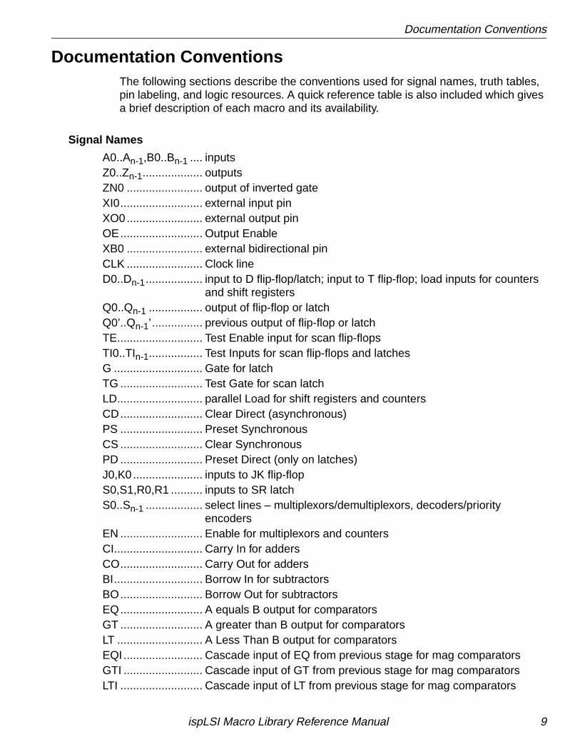
Documentation ConventionsThe following sections describe the conventions used for signal names, truth tables,pin labeling, and logic resources. A quick reference table is also included which givesa brief description of each macro and its availability.
Signal Names
A0..An-1,B0..Bn-1 .... inputsZ0..Zn-1................... outputsZN0 ........................ output of inverted gateXI0.......................... external input pinXO0........................ external output pinOE.......................... Output EnableXB0 ........................ external bidirectional pinCLK ........................ Clock lineD0..Dn-1.................. input to D flip-flop/latch; input to T flip-flop; load inputs for counters
and shift registersQ0..Qn-1 ................. output of flip-flop or latchQ0’..Qn-1’................ previous output of flip-flop or latchTE........................... Test Enable input for scan flip-flopsTI0..TIn-1................. Test Inputs for scan flip-flops and latchesG ............................ Gate for latchTG .......................... Test Gate for scan latchLD........................... parallel Load for shift registers and countersCD.......................... Clear Direct (asynchronous)PS .......................... Preset SynchronousCS .......................... Clear SynchronousPD .......................... Preset Direct (only on latches)J0,K0...................... inputs to JK flip-flopS0,S1,R0,R1 .......... inputs to SR latchS0..Sn-1 .................. select lines – multiplexors/demultiplexors, decoders/priority
encodersEN .......................... Enable for multiplexors and countersCI............................ Carry In for addersCO.......................... Carry Out for addersBI............................ Borrow In for subtractorsBO.......................... Borrow Out for subtractorsEQ.......................... A equals B output for comparatorsGT .......................... A greater than B output for comparatorsLT ........................... A Less Than B output for comparatorsEQI ......................... Cascade input of EQ from previous stage for mag comparatorsGTI ......................... Cascade input of GT from previous stage for mag comparatorsLTI .......................... Cascade input of LT from previous stage for mag comparators
ispLSI Macro Library Reference Manual 9
Documentation Conventions
CAI ......................... shift registers: serial input; counters: CAscade InCAIR....................... shift right serial inputCAIL ....................... shift left serial inputRL........................... shift Right/shift Left control for SRRL shift registersCAO ....................... CAscade Out for countersDNUP..................... count Down/count UP control for up-down counters
ispLSI Macro Library Reference Manual 10
Documentation Conventions
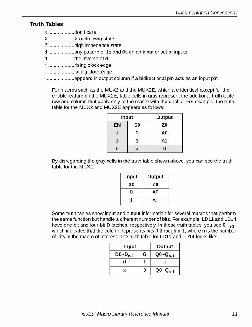
Truth Tablesx ...................don’t careX...................X (unknown) stateZ...................high impedance stated ...................any pattern of 1s and 0s on an input or set of inputsd ...................the inverse of d↑ ...................rising clock edge↓ ...................falling clock edge- ....................appears in output column if a bidirectional pin acts as an input pin
For macros such as the MUX2 and the MUX2E, which are identical except for theenable feature on the MUX2E, table cells in gray represent the additional truth tablerow and column that apply only to the macro with the enable. For example, the truthtable for the MUX2 and MUX2E appears as follows:
By disregarding the gray cells in the truth table shown above, you can see the truthtable for the MUX2.
Some truth tables show input and output information for several macros that performthe same function but handle a different number of bits. For example, LD11 and LD14have one-bit and four-bit D latches, respectively. In these truth tables, you see 0~n-1,which indicates that the column represents bits 0 through n-1, where n is the numberof bits in the macro of interest. The truth table for LD11 and LD14 looks like:
Input Output
EN S0 Z0
1 0 A0
1 1 A1
0 x 0
Input Output
S0 Z0
0 A0
1 A1
Input Output
D0~Dn-1 G Q0~Qn-1
d 1 d
x 0 Q0~Qn-1
ispLSI Macro Library Reference Manual 11
Documentation Conventions
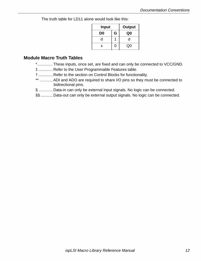
The truth table for LD11 alone would look like this:
Module Macro Truth Tables*.............. These inputs, once set, are fixed and can only be connected to VCC/GND.‡ ............. Refer to the User Programmable Features table.† ............. Refer to the section on Control Blocks for functionality.** ............ ADI and ADO are required to share I/O pins so they must be connected to
bidirectional pins.§ ............. Data-in can only be external input signals. No logic can be connected.§§ ........... Data-out can only be external output signals. No logic can be connected.
Input Output
D0 G Q0
d 1 d
x 0 Q0
ispLSI Macro Library Reference Manual 12
Documentation Conventions
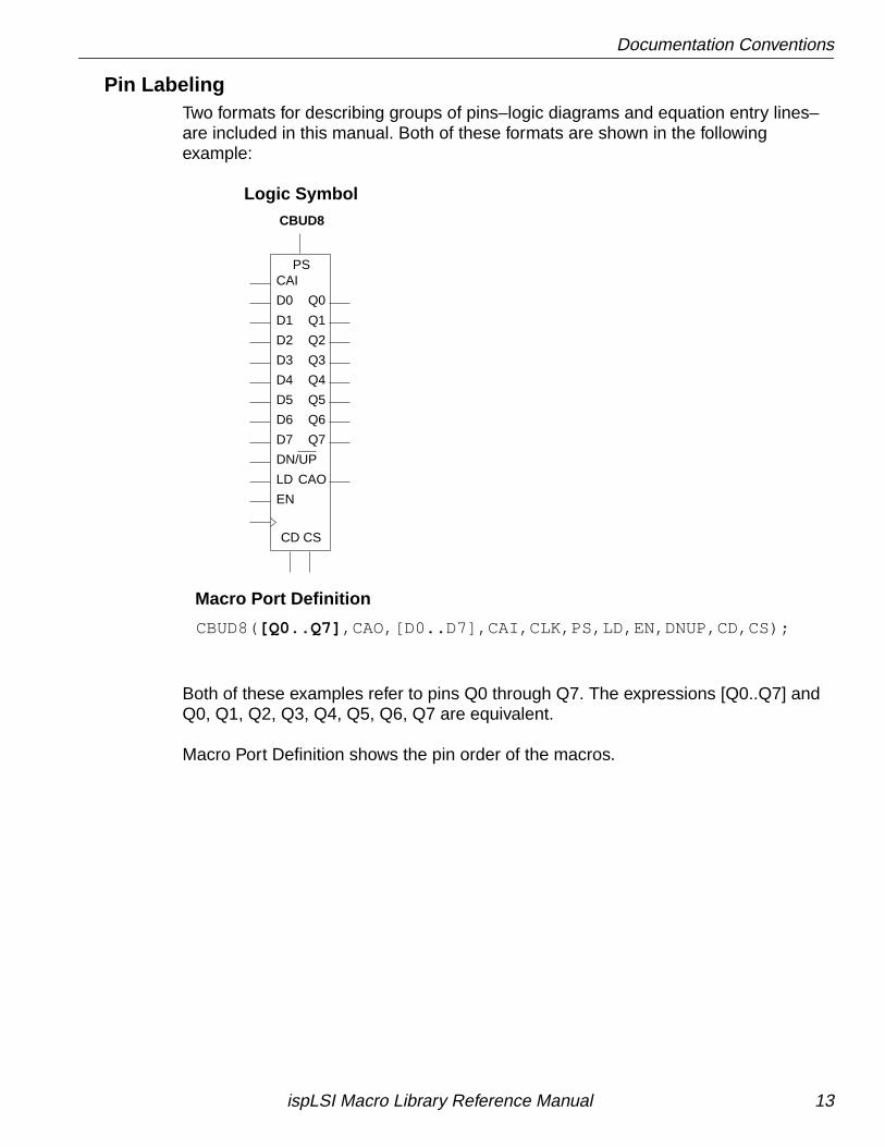
Pin LabelingTwo formats for describing groups of pins–logic diagrams and equation entry lines–are included in this manual. Both of these formats are shown in the followingexample:
Both of these examples refer to pins Q0 through Q7. The expressions [Q0..Q7] andQ0, Q1, Q2, Q3, Q4, Q5, Q6, Q7 are equivalent.
Macro Port Definition shows the pin order of the macros.
CBUD8
CBUD8([Q0..Q7] ,CAO,[D0..D7],CAI,CLK,PS,LD,EN,DNUP,CD,CS);
Macro Port Definition
Logic Symbol
DN/UP
PS
CSCD
D0
D1
D2
D3
D4
D5
D6
LD
D7
CAI
EN
Q7
Q6
Q5
Q4
Q3
Q2
Q1
CAO
Q0
ispLSI Macro Library Reference Manual 13
Documentation Conventions
Logic ResourcesThe logic resources of each macro are described as follows:
Product Terms (PTs) The number of gates in the AND array of theGLBs used by the macro. Add one product termif you use the Product Term Clock option withthe macro or if the macro has an asynchronousclear (CD). If “/out” follows the number ofproduct terms, it means the “number of productterms per output.”
Generic Logic Blocks(GLB) The number of GLBs that the macro uses.
GLB Outputs (Outputs) The number of GLB outputs the macro uses,including outputs internal to the macro. A GLBoutput is also called an Output Logic Macrocell(OLMC).
GLB Levels (Levels) The number of levels of GLBs (not gates) used.
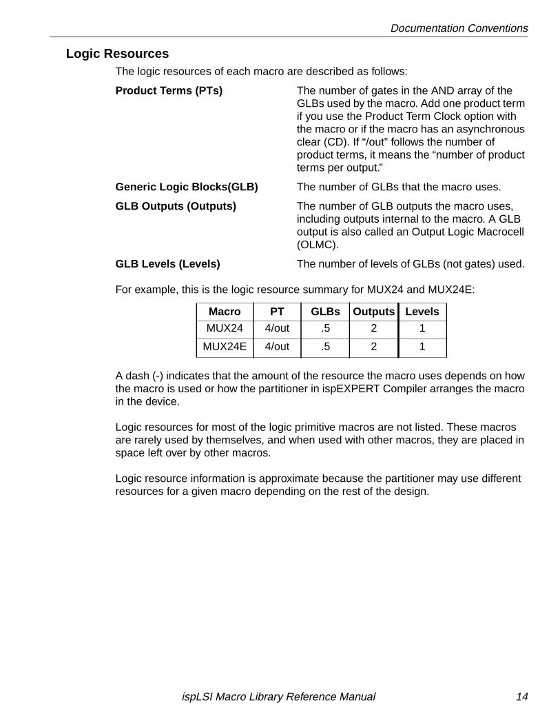
For example, this is the logic resource summary for MUX24 and MUX24E:
A dash (-) indicates that the amount of the resource the macro uses depends on howthe macro is used or how the partitioner in ispEXPERT Compiler arranges the macroin the device.
Logic resources for most of the logic primitive macros are not listed. These macrosare rarely used by themselves, and when used with other macros, they are placed inspace left over by other macros.
Logic resource information is approximate because the partitioner may use differentresources for a given macro depending on the rest of the design.
Macro PT GLBs Outputs Levels
MUX24 4/out .5 2 1
MUX24E 4/out .5 2 1
ispLSI Macro Library Reference Manual 14
Documentation Conventions
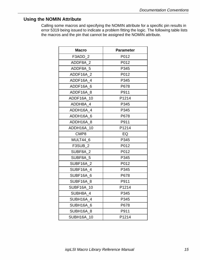
Using the NOMIN AttributeCalling some macros and specifying the NOMIN attribute for a specific pin results inerror 5319 being issued to indicate a problem fitting the logic. The following table liststhe macros and the pin that cannot be assigned the NOMIN attribute.
Macro Parameter
F3ADD_2 P012
ADDF8A_2 P012
ADDF8A_5 P345
ADDF16A_2 P012
ADDF16A_4 P345
ADDF16A_6 P678
ADDF16A_8 P911
ADDF16A_10 P1214
ADDH8A_4 P345
ADDH16A_4 P345
ADDH16A_6 P678
ADDH16A_8 P911
ADDH16A_10 P1214
CMP8 EQ
MULT44_6 P345
F3SUB_2 P012
SUBF8A_2 P012
SUBF8A_5 P345
SUBF16A_2 P012
SUBF16A_4 P345
SUBF16A_6 P678
SUBF16A_8 P911
SUBF16A_10 P1214
SUBH8A_4 P345
SUBH16A_4 P345
SUBH16A_6 P678
SUBH16A_8 P911
SUBH16A_10 P1214
ispLSI Macro Library Reference Manual 15
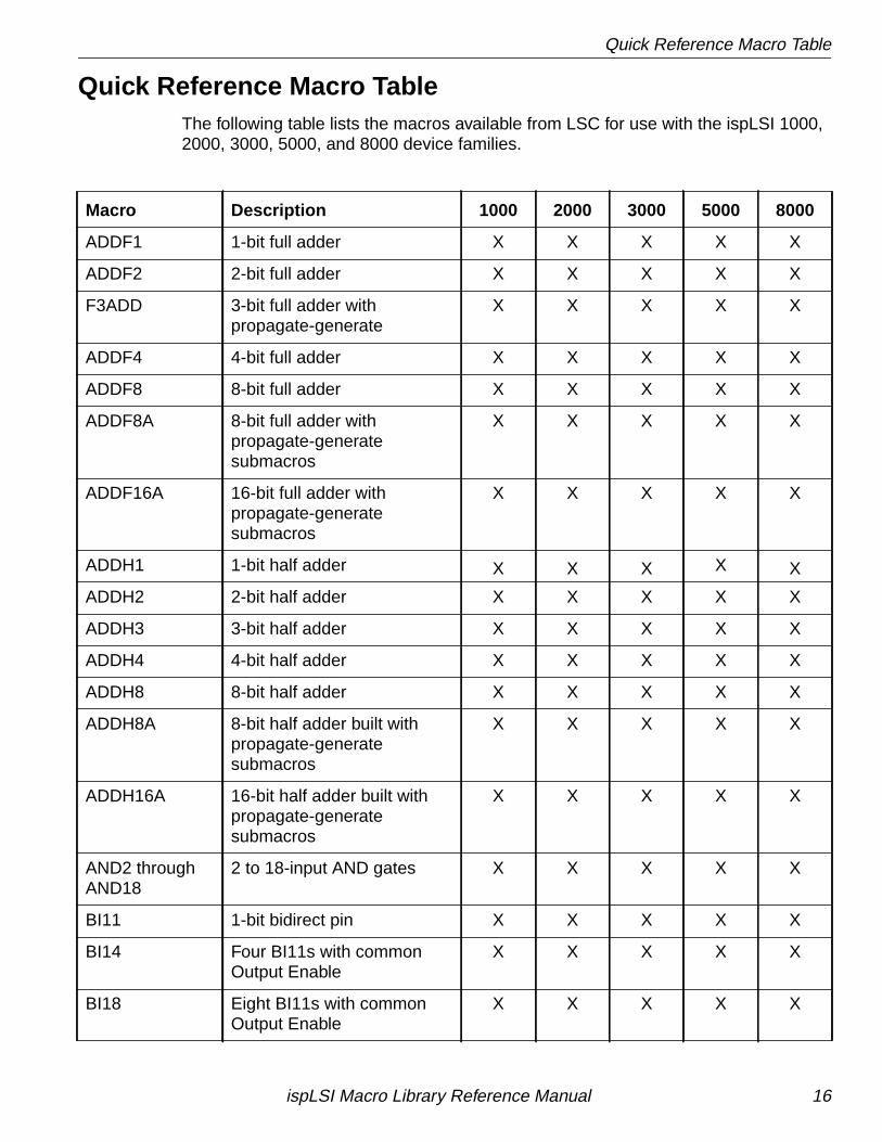
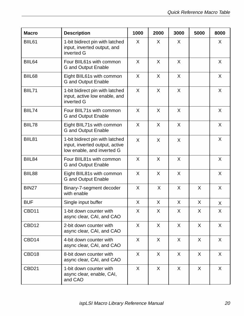
Quick Reference Macro Table
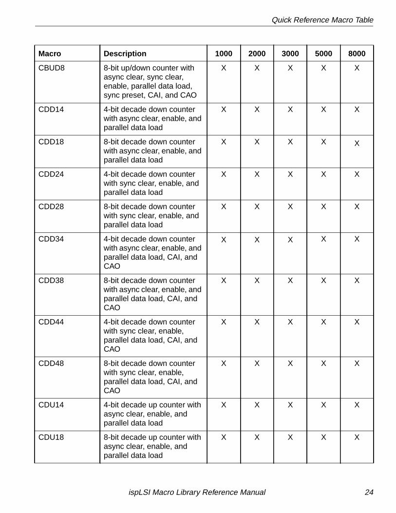
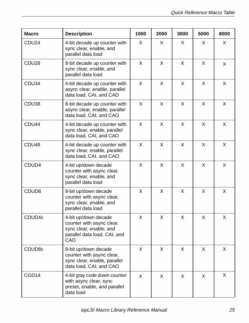
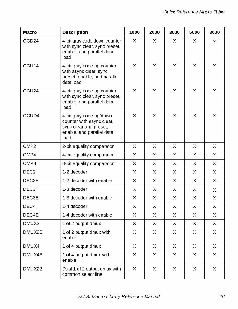
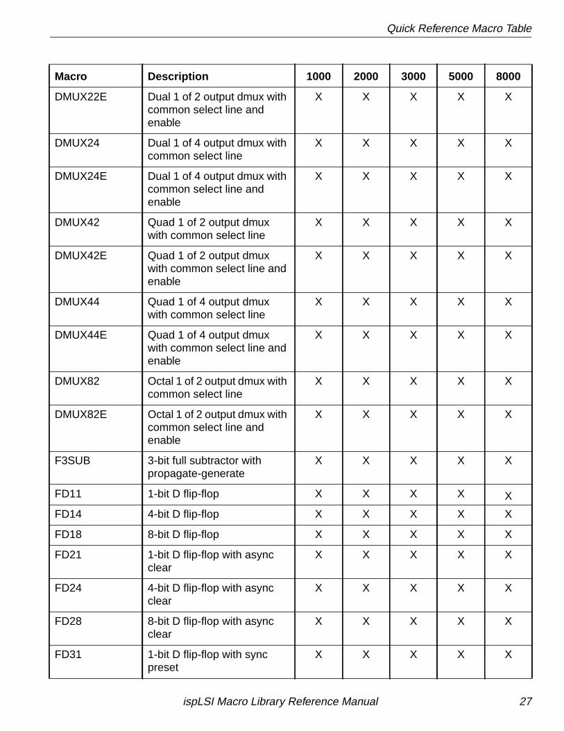
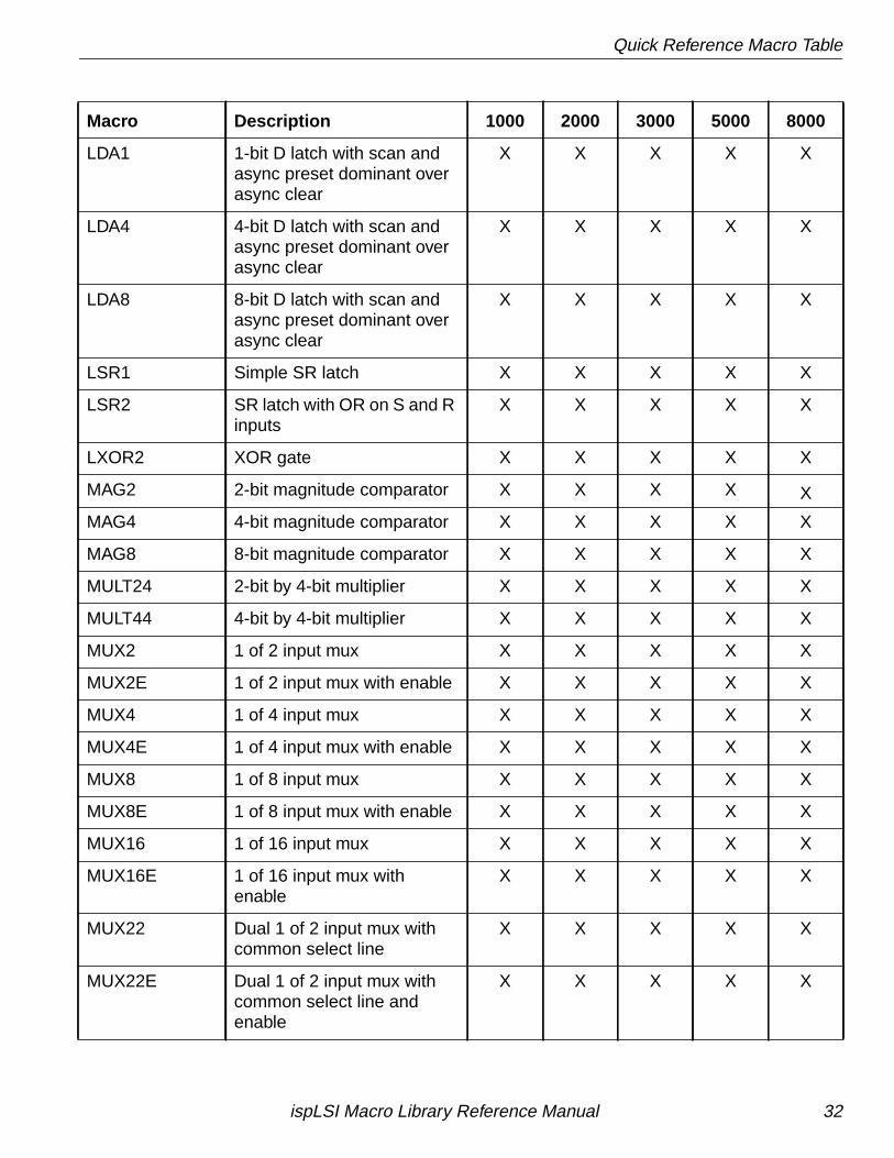
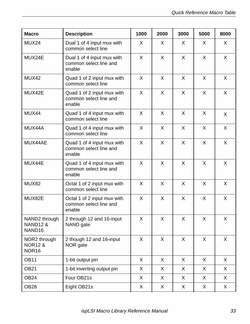
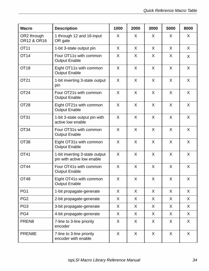
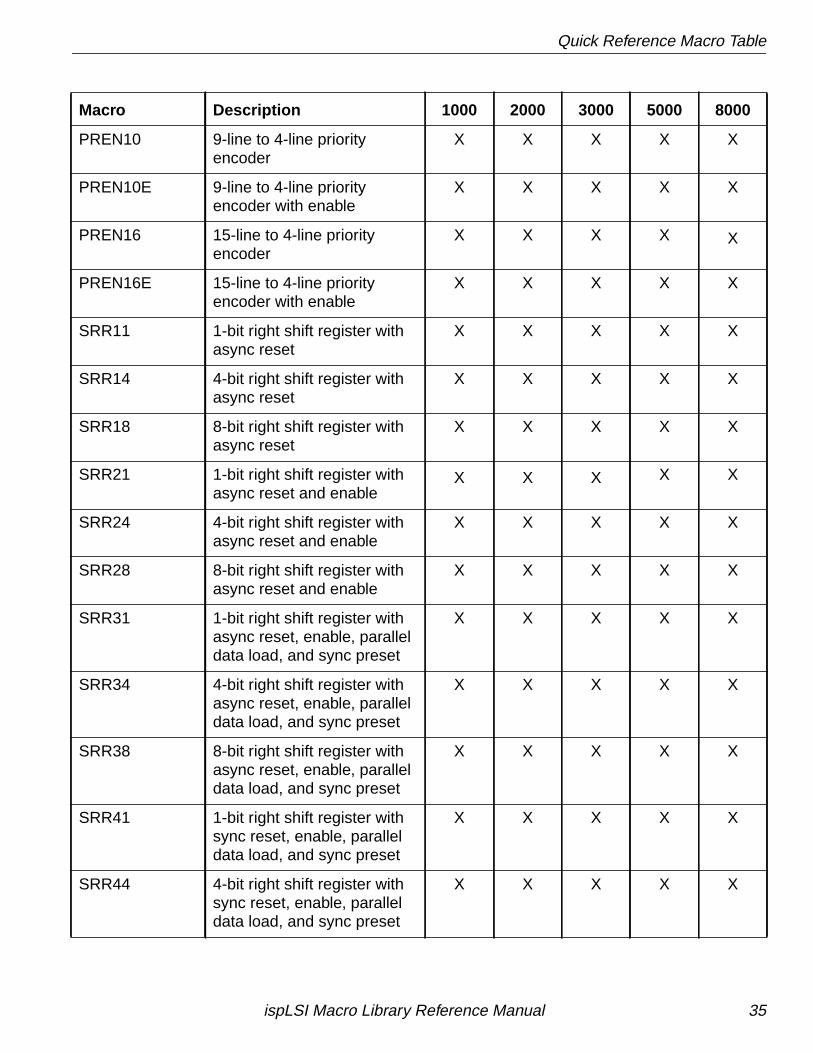
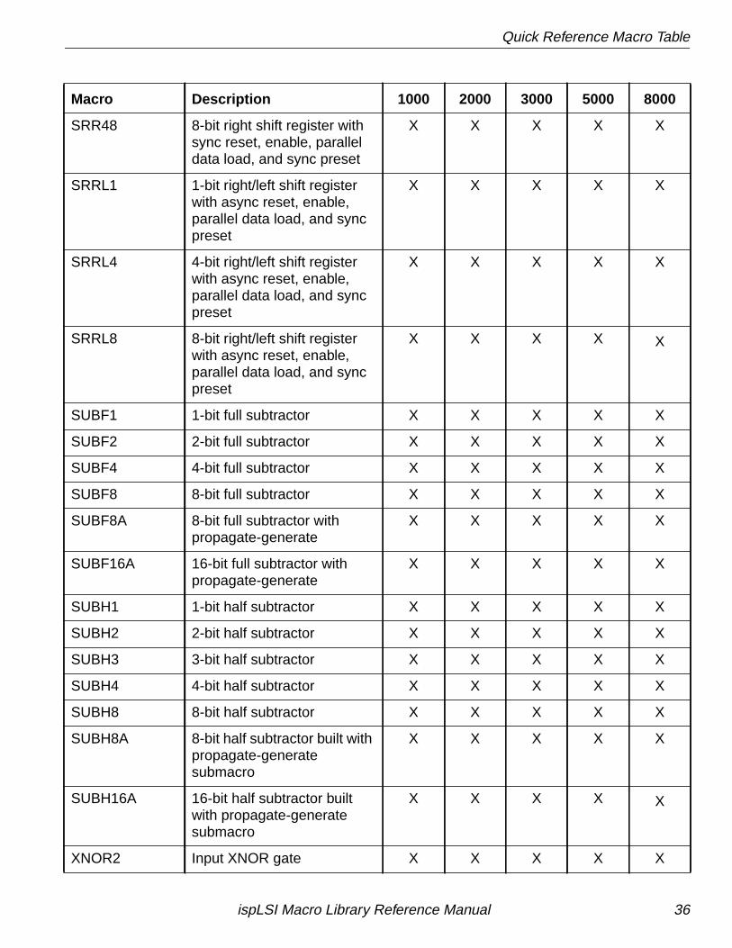
Quick Reference Macro TableThe following table lists the macros available from LSC for use with the ispLSI 1000,2000, 3000, 5000, and 8000 device families.
Macro Description 1000 2000 3000 5000 8000
ADDF1 1-bit full adder X X X X X
ADDF2 2-bit full adder X X X X X
F3ADD 3-bit full adder withpropagate-generate
X X X X X
ADDF4 4-bit full adder X X X X X
ADDF8 8-bit full adder X X X X X
ADDF8A 8-bit full adder withpropagate-generatesubmacros
X X X X X
ADDF16A 16-bit full adder withpropagate-generatesubmacros
X X X X X
ADDH1 1-bit half adder X X X X X
ADDH2 2-bit half adder X X X X X
ADDH3 3-bit half adder X X X X X
ADDH4 4-bit half adder X X X X X
ADDH8 8-bit half adder X X X X X
ADDH8A 8-bit half adder built withpropagate-generatesubmacros
X X X X X
ADDH16A 16-bit half adder built withpropagate-generatesubmacros
X X X X X
AND2 throughAND18
2 to 18-input AND gates X X X X X
BI11 1-bit bidirect pin X X X X X
BI14 Four BI11s with commonOutput Enable
X X X X X
BI18 Eight BI11s with commonOutput Enable
X X X X X
ispLSI Macro Library Reference Manual 16
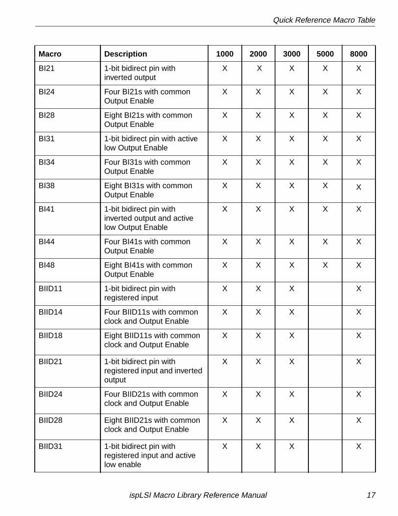
Quick Reference Macro Table
BI21 1-bit bidirect pin withinverted output
X X X X X
BI24 Four BI21s with commonOutput Enable
X X X X X
BI28 Eight BI21s with commonOutput Enable
X X X X X
BI31 1-bit bidirect pin with activelow Output Enable
X X X X X
BI34 Four BI31s with commonOutput Enable
X X X X X
BI38 Eight BI31s with commonOutput Enable
X X X X X
BI41 1-bit bidirect pin withinverted output and activelow Output Enable
X X X X X
BI44 Four BI41s with commonOutput Enable
X X X X X
BI48 Eight BI41s with commonOutput Enable
X X X X X
BIID11 1-bit bidirect pin withregistered input
X X X X
BIID14 Four BIID11s with commonclock and Output Enable
X X X X
BIID18 Eight BIID11s with commonclock and Output Enable
X X X X
BIID21 1-bit bidirect pin withregistered input and invertedoutput
X X X X
BIID24 Four BIID21s with commonclock and Output Enable
X X X X
BIID28 Eight BIID21s with commonclock and Output Enable
X X X X
BIID31 1-bit bidirect pin withregistered input and activelow enable
X X X X
Macro Description 1000 2000 3000 5000 8000
ispLSI Macro Library Reference Manual 17
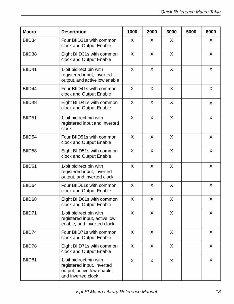
Quick Reference Macro Table
BIID34 Four BIID31s with commonclock and Output Enable
X X X X
BIID38 Eight BIID31s with commonclock and Output Enable
X X X X
BIID41 1-bit bidirect pin withregistered input, invertedoutput, and active low enable
X X X X
BIID44 Four BIID41s with commonclock and Output Enable
X X X X
BIID48 Eight BIID41s with commonclock and Output Enable
X X X X
BIID51 1-bit bidirect pin withregistered input and invertedclock
X X X X
BIID54 Four BIID51s with commonclock and Output Enable
X X X X
BIID58 Eight BIID51s with commonclock and Output Enable
X X X X
BIID61 1-bit bidirect pin withregistered input, invertedoutput, and inverted clock
X X X X
BIID64 Four BIID61s with commonclock and Output Enable
X X X X
BIID68 Eight BIID61s with commonclock and Output Enable
X X X X
BIID71 1-bit bidirect pin withregistered input, active lowenable, and inverted clock
X X X X
BIID74 Four BIID71s with commonclock and Output Enable
X X X X
BIID78 Eight BIID71s with commonclock and Output Enable
X X X X
BIID81 1-bit bidirect pin withregistered input, invertedoutput, active low enable,and inverted clock
X X X X
Macro Description 1000 2000 3000 5000 8000
ispLSI Macro Library Reference Manual 18
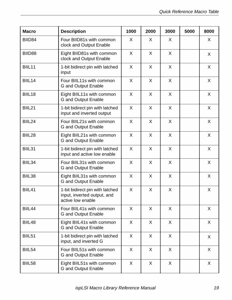
Quick Reference Macro Table
BIID84 Four BIID81s with commonclock and Output Enable
X X X X
BIID88 Eight BIID81s with commonclock and Output Enable
X X X X
BIIL11 1-bit bidirect pin with latchedinput
X X X X
BIIL14 Four BIIL11s with commonG and Output Enable
X X X X
BIIL18 Eight BIIL11s with commonG and Output Enable
X X X X
BIIL21 1-bit bidirect pin with latchedinput and inverted output
X X X X
BIIL24 Four BIIL21s with commonG and Output Enable
X X X X
BIIL28 Eight BIIL21s with commonG and Output Enable
X X X X
BIIL31 1-bit bidirect pin with latchedinput and active low enable
X X X X
BIIL34 Four BIIL31s with commonG and Output Enable
X X X X
BIIL38 Eight BIIL31s with commonG and Output Enable
X X X X
BIIL41 1-bit bidirect pin with latchedinput, inverted output, andactive low enable
X X X X
BIIL44 Four BIIL41s with commonG and Output Enable
X X X X
BIIL48 Eight BIIL41s with commonG and Output Enable
X X X X
BIIL51 1-bit bidirect pin with latchedinput, and inverted G
X X X X
BIIL54 Four BIIL51s with commonG and Output Enable
X X X X
BIIL58 Eight BIIL51s with commonG and Output Enable
X X X X
Macro Description 1000 2000 3000 5000 8000
ispLSI Macro Library Reference Manual 19
Quick Reference Macro Table
BIIL61 1-bit bidirect pin with latchedinput, inverted output, andinverted G
X X X X
BIIL64 Four BIIL61s with commonG and Output Enable
X X X X
BIIL68 Eight BIIL61s with commonG and Output Enable
X X X X
BIIL71 1-bit bidirect pin with latchedinput, active low enable, andinverted G
X X X X
BIIL74 Four BIIL71s with commonG and Output Enable
X X X X
BIIL78 Eight BIIL71s with commonG and Output Enable
X X X X
BIIL81 1-bit bidirect pin with latchedinput, inverted output, activelow enable, and inverted G
X X X X
BIIL84 Four BIIL81s with commonG and Output Enable
X X X X
BIIL88 Eight BIIL81s with commonG and Output Enable
X X X X
BIN27 Binary-7-segment decoderwith enable
X X X X X
BUF Single input buffer X X X X X
CBD11 1-bit down counter withasync clear, CAI, and CAO
X X X X X
CBD12 2-bit down counter withasync clear, CAI, and CAO
X X X X X
CBD14 4-bit down counter withasync clear, CAI, and CAO
X X X X X
CBD18 8-bit down counter withasync clear, CAI, and CAO
X X X X X
CBD21 1-bit down counter withasync clear, enable, CAI,and CAO
X X X X X
Macro Description 1000 2000 3000 5000 8000
ispLSI Macro Library Reference Manual 20
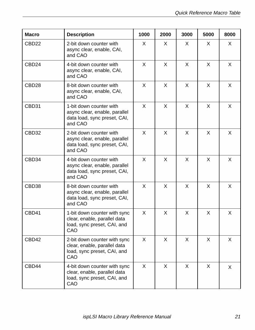
Quick Reference Macro Table
CBD22 2-bit down counter withasync clear, enable, CAI,and CAO
X X X X X
CBD24 4-bit down counter withasync clear, enable, CAI,and CAO
X X X X X
CBD28 8-bit down counter withasync clear, enable, CAI,and CAO
X X X X X
CBD31 1-bit down counter withasync clear, enable, paralleldata load, sync preset, CAI,and CAO
X X X X X
CBD32 2-bit down counter withasync clear, enable, paralleldata load, sync preset, CAI,and CAO
X X X X X
CBD34 4-bit down counter withasync clear, enable, paralleldata load, sync preset, CAI,and CAO
X X X X X
CBD38 8-bit down counter withasync clear, enable, paralleldata load, sync preset, CAI,and CAO
X X X X X
CBD41 1-bit down counter with syncclear, enable, parallel dataload, sync preset, CAI, andCAO
X X X X X
CBD42 2-bit down counter with syncclear, enable, parallel dataload, sync preset, CAI, andCAO
X X X X X
CBD44 4-bit down counter with syncclear, enable, parallel dataload, sync preset, CAI, andCAO
X X X X X
Macro Description 1000 2000 3000 5000 8000
ispLSI Macro Library Reference Manual 21
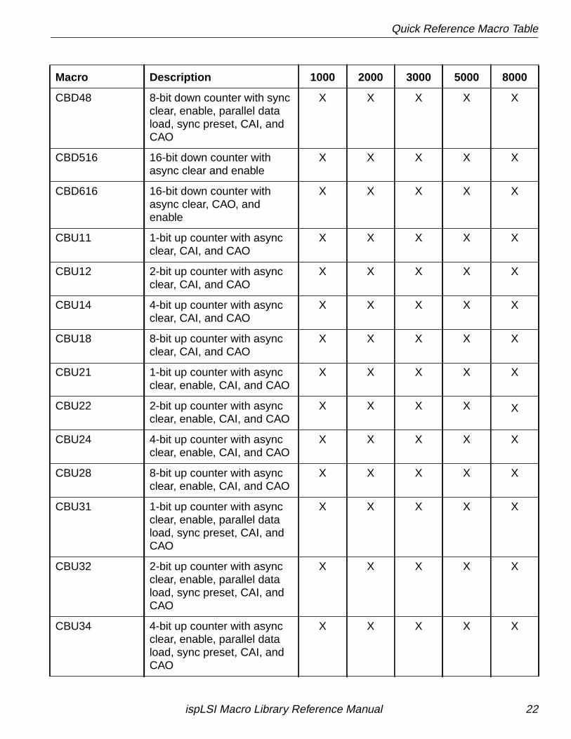
Quick Reference Macro Table
CBD48 8-bit down counter with syncclear, enable, parallel dataload, sync preset, CAI, andCAO
X X X X X
CBD516 16-bit down counter withasync clear and enable
X X X X X
CBD616 16-bit down counter withasync clear, CAO, andenable
X X X X X
CBU11 1-bit up counter with asyncclear, CAI, and CAO
X X X X X
CBU12 2-bit up counter with asyncclear, CAI, and CAO
X X X X X
CBU14 4-bit up counter with asyncclear, CAI, and CAO
X X X X X
CBU18 8-bit up counter with asyncclear, CAI, and CAO
X X X X X
CBU21 1-bit up counter with asyncclear, enable, CAI, and CAO
X X X X X
CBU22 2-bit up counter with asyncclear, enable, CAI, and CAO
X X X X X
CBU24 4-bit up counter with asyncclear, enable, CAI, and CAO
X X X X X
CBU28 8-bit up counter with asyncclear, enable, CAI, and CAO
X X X X X
CBU31 1-bit up counter with asyncclear, enable, parallel dataload, sync preset, CAI, andCAO
X X X X X
CBU32 2-bit up counter with asyncclear, enable, parallel dataload, sync preset, CAI, andCAO
X X X X X
CBU34 4-bit up counter with asyncclear, enable, parallel dataload, sync preset, CAI, andCAO
X X X X X
Macro Description 1000 2000 3000 5000 8000
ispLSI Macro Library Reference Manual 22
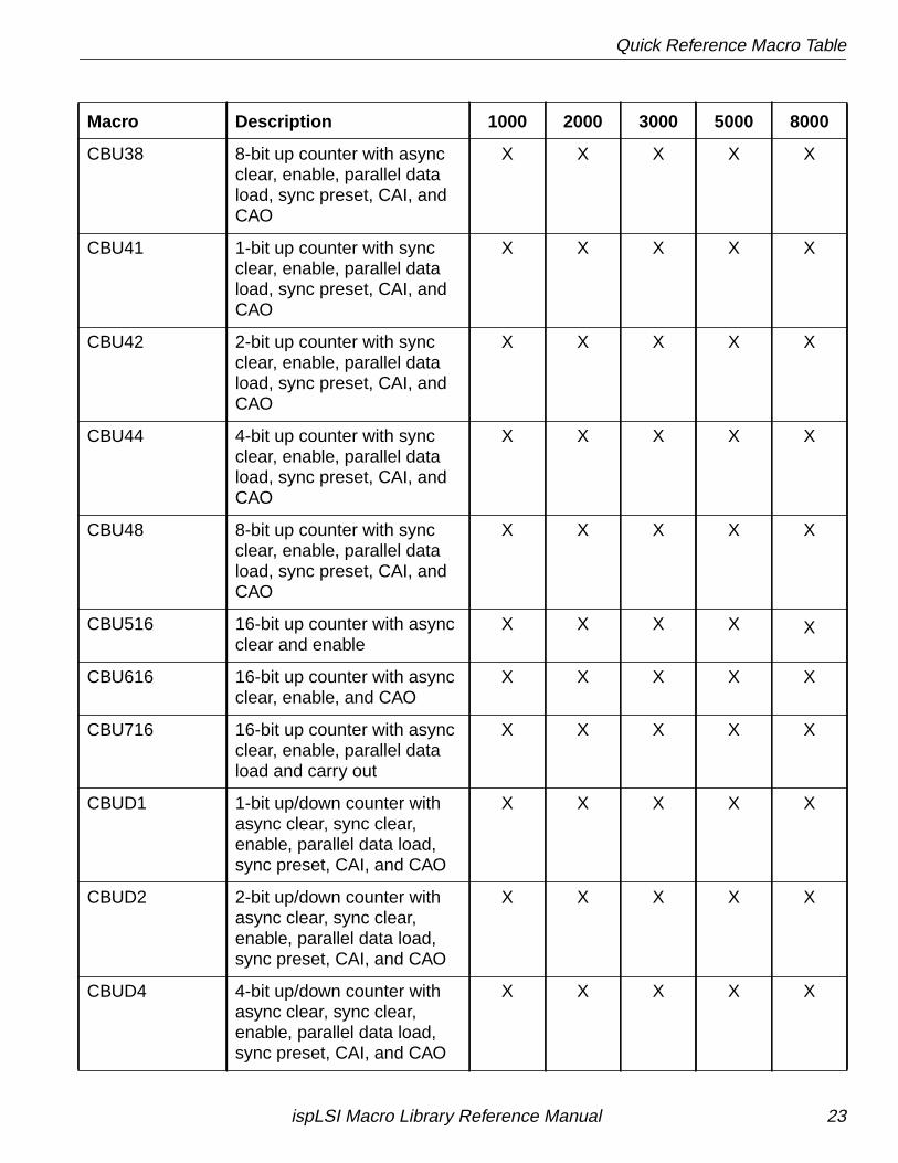
Quick Reference Macro Table
CBU38 8-bit up counter with asyncclear, enable, parallel dataload, sync preset, CAI, andCAO
X X X X X
CBU41 1-bit up counter with syncclear, enable, parallel dataload, sync preset, CAI, andCAO
X X X X X
CBU42 2-bit up counter with syncclear, enable, parallel dataload, sync preset, CAI, andCAO
X X X X X
CBU44 4-bit up counter with syncclear, enable, parallel dataload, sync preset, CAI, andCAO
X X X X X
CBU48 8-bit up counter with syncclear, enable, parallel dataload, sync preset, CAI, andCAO
X X X X X
CBU516 16-bit up counter with asyncclear and enable
X X X X X
CBU616 16-bit up counter with asyncclear, enable, and CAO
X X X X X
CBU716 16-bit up counter with asyncclear, enable, parallel dataload and carry out
X X X X X
CBUD1 1-bit up/down counter withasync clear, sync clear,enable, parallel data load,sync preset, CAI, and CAO
X X X X X
CBUD2 2-bit up/down counter withasync clear, sync clear,enable, parallel data load,sync preset, CAI, and CAO
X X X X X
CBUD4 4-bit up/down counter withasync clear, sync clear,enable, parallel data load,sync preset, CAI, and CAO
X X X X X
Macro Description 1000 2000 3000 5000 8000
ispLSI Macro Library Reference Manual 23
Quick Reference Macro Table
CBUD8 8-bit up/down counter withasync clear, sync clear,enable, parallel data load,sync preset, CAI, and CAO
X X X X X
CDD14 4-bit decade down counterwith async clear, enable, andparallel data load
X X X X X
CDD18 8-bit decade down counterwith async clear, enable, andparallel data load
X X X X X
CDD24 4-bit decade down counterwith sync clear, enable, andparallel data load
X X X X X
CDD28 8-bit decade down counterwith sync clear, enable, andparallel data load
X X X X X
CDD34 4-bit decade down counterwith async clear, enable, andparallel data load, CAI, andCAO
X X X X X
CDD38 8-bit decade down counterwith async clear, enable, andparallel data load, CAI, andCAO
X X X X X
CDD44 4-bit decade down counterwith sync clear, enable,parallel data load, CAI, andCAO
X X X X X
CDD48 8-bit decade down counterwith sync clear, enable,parallel data load, CAI, andCAO
X X X X X
CDU14 4-bit decade up counter withasync clear, enable, andparallel data load
X X X X X
CDU18 8-bit decade up counter withasync clear, enable, andparallel data load
X X X X X
Macro Description 1000 2000 3000 5000 8000
ispLSI Macro Library Reference Manual 24
Quick Reference Macro Table
CDU24 4-bit decade up counter withsync clear, enable, andparallel data load
X X X X X
CDU28 8-bit decade up counter withsync clear, enable, andparallel data load
X X X X X
CDU34 4-bit decade up counter withasync clear, enable, paralleldata load, CAI, and CAO
X X X X X
CDU38 8-bit decade up counter withasync clear, enable, paralleldata load, CAI, and CAO
X X X X X
CDU44 4-bit decade up counter withsync clear, enable, paralleldata load, CAI, and CAO
X X X X X
CDU48 4-bit decade up counter withsync clear, enable, paralleldata load, CAI, and CAO
X X X X X
CDUD4 4-bit up/down decadecounter with async clear,sync clear, enable, andparallel data load
X X X X X
CDUD8 8-bit up/down decadecounter with async clear,sync clear, enable, andparallel data load
X X X X X
CDUD4c 4-bit up/down decadecounter with async clear,sync clear, enable, andparallel data load, CAI, andCAO
X X X X X
CDUD8c 8-bit up/down decadecounter with async clear,sync clear, enable, paralleldata load, CAI, and CAO
X X X X X
CGD14 4-bit gray code down counterwith async clear, syncpreset, enable, and paralleldata load
X X X X X
Macro Description 1000 2000 3000 5000 8000
ispLSI Macro Library Reference Manual 25
Quick Reference Macro Table
CGD24 4-bit gray code down counterwith sync clear, sync preset,enable, and parallel dataload
X X X X X
CGU14 4-bit gray code up counterwith async clear, syncpreset, enable, and paralleldata load
X X X X X
CGU24 4-bit gray code up counterwith sync clear, sync preset,enable, and parallel dataload
X X X X X
CGUD4 4-bit gray code up/downcounter with async clear,sync clear and preset,enable, and parallel dataload
X X X X X
CMP2 2-bit equality comparator X X X X X
CMP4 4-bit equality comparator X X X X X
CMP8 8-bit equality comparator X X X X X
DEC2 1-2 decoder X X X X X
DEC2E 1-2 decoder with enable X X X X X
DEC3 1-3 decoder X X X X X
DEC3E 1-3 decoder with enable X X X X X
DEC4 1-4 decoder X X X X X
DEC4E 1-4 decoder with enable X X X X X
DMUX2 1 of 2 output dmux X X X X X
DMUX2E 1 of 2 output dmux withenable
X X X X X
DMUX4 1 of 4 output dmux X X X X X
DMUX4E 1 of 4 output dmux withenable
X X X X X
DMUX22 Dual 1 of 2 output dmux withcommon select line
X X X X X
Macro Description 1000 2000 3000 5000 8000
ispLSI Macro Library Reference Manual 26
Quick Reference Macro Table
DMUX22E Dual 1 of 2 output dmux withcommon select line andenable
X X X X X
DMUX24 Dual 1 of 4 output dmux withcommon select line
X X X X X
DMUX24E Dual 1 of 4 output dmux withcommon select line andenable
X X X X X
DMUX42 Quad 1 of 2 output dmuxwith common select line
X X X X X
DMUX42E Quad 1 of 2 output dmuxwith common select line andenable
X X X X X
DMUX44 Quad 1 of 4 output dmuxwith common select line
X X X X X
DMUX44E Quad 1 of 4 output dmuxwith common select line andenable
X X X X X
DMUX82 Octal 1 of 2 output dmux withcommon select line
X X X X X
DMUX82E Octal 1 of 2 output dmux withcommon select line andenable
X X X X X
F3SUB 3-bit full subtractor withpropagate-generate
X X X X X
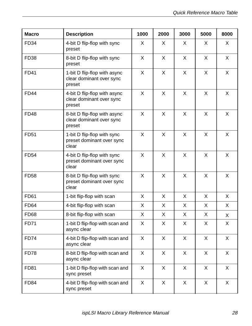
FD11 1-bit D flip-flop X X X X X
FD14 4-bit D flip-flop X X X X X
FD18 8-bit D flip-flop X X X X X
FD21 1-bit D flip-flop with asyncclear
X X X X X
FD24 4-bit D flip-flop with asyncclear
X X X X X
FD28 8-bit D flip-flop with asyncclear
X X X X X
FD31 1-bit D flip-flop with syncpreset
X X X X X
Macro Description 1000 2000 3000 5000 8000
ispLSI Macro Library Reference Manual 27
Quick Reference Macro Table
FD34 4-bit D flip-flop with syncpreset
X X X X X
FD38 8-bit D flip-flop with syncpreset
X X X X X
FD41 1-bit D flip-flop with asyncclear dominant over syncpreset
X X X X X
FD44 4-bit D flip-flop with asyncclear dominant over syncpreset
X X X X X
FD48 8-bit D flip-flop with asyncclear dominant over syncpreset
X X X X X
FD51 1-bit D flip-flop with syncpreset dominant over syncclear
X X X X X
FD54 4-bit D flip-flop with syncpreset dominant over syncclear
X X X X X
FD58 8-bit D flip-flop with syncpreset dominant over syncclear
X X X X X
FD61 1-bit flip-flop with scan X X X X X
FD64 4-bit flip-flop with scan X X X X X
FD68 8-bit flip-flop with scan X X X X X
FD71 1-bit D flip-flop with scan andasync clear
X X X X X
FD74 4-bit D flip-flop with scan andasync clear
X X X X X
FD78 8-bit D flip-flop with scan andasync clear
X X X X X
FD81 1-bit D flip-flop with scan andsync preset
X X X X X
FD84 4-bit D flip-flop with scan andsync preset
X X X X X
Macro Description 1000 2000 3000 5000 8000
ispLSI Macro Library Reference Manual 28
Quick Reference Macro Table
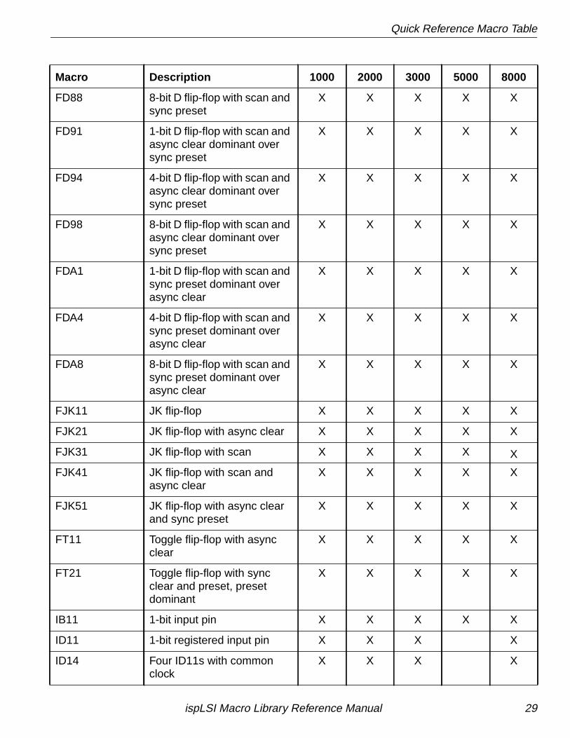
FD88 8-bit D flip-flop with scan andsync preset
X X X X X
FD91 1-bit D flip-flop with scan andasync clear dominant oversync preset
X X X X X
FD94 4-bit D flip-flop with scan andasync clear dominant oversync preset
X X X X X
FD98 8-bit D flip-flop with scan andasync clear dominant oversync preset
X X X X X
FDA1 1-bit D flip-flop with scan andsync preset dominant overasync clear
X X X X X
FDA4 4-bit D flip-flop with scan andsync preset dominant overasync clear
X X X X X
FDA8 8-bit D flip-flop with scan andsync preset dominant overasync clear
X X X X X
FJK11 JK flip-flop X X X X X
FJK21 JK flip-flop with async clear X X X X X
FJK31 JK flip-flop with scan X X X X X
FJK41 JK flip-flop with scan andasync clear
X X X X X
FJK51 JK flip-flop with async clearand sync preset
X X X X X
FT11 Toggle flip-flop with asyncclear
X X X X X
FT21 Toggle flip-flop with syncclear and preset, presetdominant
X X X X X
IB11 1-bit input pin X X X X X
ID11 1-bit registered input pin X X X X
ID14 Four ID11s with commonclock
X X X X
Macro Description 1000 2000 3000 5000 8000
ispLSI Macro Library Reference Manual 29
Quick Reference Macro Table
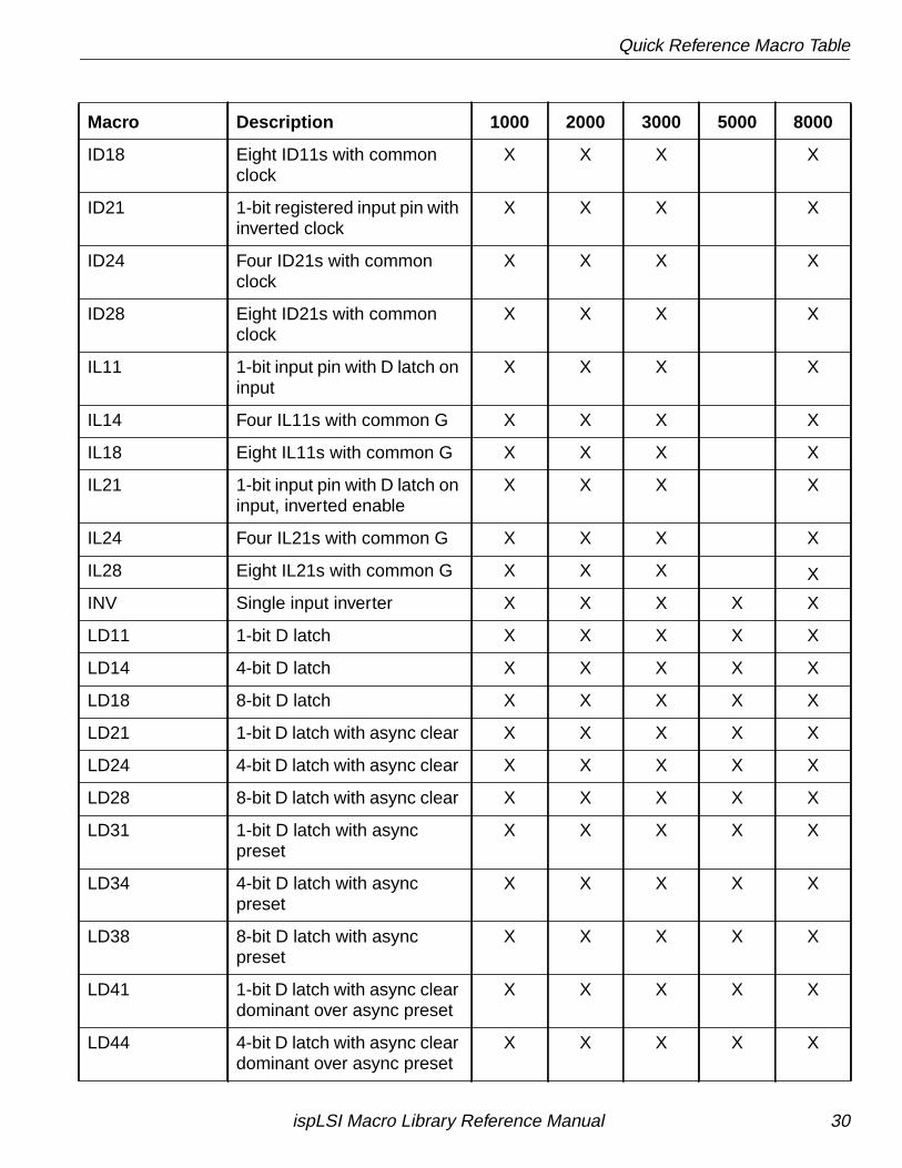
ID18 Eight ID11s with commonclock
X X X X
ID21 1-bit registered input pin withinverted clock
X X X X
ID24 Four ID21s with commonclock
X X X X
ID28 Eight ID21s with commonclock
X X X X
IL11 1-bit input pin with D latch oninput
X X X X
IL14 Four IL11s with common G X X X X
IL18 Eight IL11s with common G X X X X
IL21 1-bit input pin with D latch oninput, inverted enable
X X X X
IL24 Four IL21s with common G X X X X
IL28 Eight IL21s with common G X X X X
INV Single input inverter X X X X X
LD11 1-bit D latch X X X X X
LD14 4-bit D latch X X X X X
LD18 8-bit D latch X X X X X
LD21 1-bit D latch with async clear X X X X X
LD24 4-bit D latch with async clear X X X X X
LD28 8-bit D latch with async clear X X X X X
LD31 1-bit D latch with asyncpreset
X X X X X
LD34 4-bit D latch with asyncpreset
X X X X X
LD38 8-bit D latch with asyncpreset
X X X X X
LD41 1-bit D latch with async cleardominant over async preset
X X X X X
LD44 4-bit D latch with async cleardominant over async preset
X X X X X
Macro Description 1000 2000 3000 5000 8000
ispLSI Macro Library Reference Manual 30
Quick Reference Macro Table
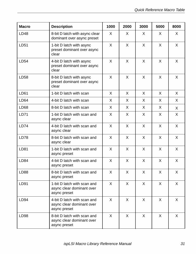
LD48 8-bit D latch with async cleardominant over async preset
X X X X X
LD51 1-bit D latch with asyncpreset dominant over asyncclear
X X X X X
LD54 4-bit D latch with asyncpreset dominant over asyncclear
X X X X X
LD58 8-bit D latch with asyncpreset dominant over asyncclear
X X X X X
LD61 1-bit D latch with scan X X X X X
LD64 4-bit D latch with scan X X X X X
LD68 8-bit D latch with scan X X X X X
LD71 1-bit D latch with scan andasync clear
X X X X X
LD74 4-bit D latch with scan andasync clear
X X X X X
LD78 8-bit D latch with scan andasync clear
X X X X X
LD81 1-bit D latch with scan andasync preset
X X X X X
LD84 4-bit D latch with scan andasync preset
X X X X X
LD88 8-bit D latch with scan andasync preset
X X X X X
LD91 1-bit D latch with scan andasync clear dominant overasync preset
X X X X X
LD94 4-bit D latch with scan andasync clear dominant overasync preset
X X X X X
LD98 8-bit D latch with scan andasync clear dominant overasync preset
X X X X X
Macro Description 1000 2000 3000 5000 8000
ispLSI Macro Library Reference Manual 31
Quick Reference Macro Table
LDA1 1-bit D latch with scan andasync preset dominant overasync clear
X X X X X
LDA4 4-bit D latch with scan andasync preset dominant overasync clear
X X X X X
LDA8 8-bit D latch with scan andasync preset dominant overasync clear
X X X X X
LSR1 Simple SR latch X X X X X
LSR2 SR latch with OR on S and Rinputs
X X X X X
LXOR2 XOR gate X X X X X
MAG2 2-bit magnitude comparator X X X X X
MAG4 4-bit magnitude comparator X X X X X
MAG8 8-bit magnitude comparator X X X X X
MULT24 2-bit by 4-bit multiplier X X X X X
MULT44 4-bit by 4-bit multiplier X X X X X
MUX2 1 of 2 input mux X X X X X
MUX2E 1 of 2 input mux with enable X X X X X
MUX4 1 of 4 input mux X X X X X
MUX4E 1 of 4 input mux with enable X X X X X
MUX8 1 of 8 input mux X X X X X
MUX8E 1 of 8 input mux with enable X X X X X
MUX16 1 of 16 input mux X X X X X
MUX16E 1 of 16 input mux withenable
X X X X X
MUX22 Dual 1 of 2 input mux withcommon select line
X X X X X
MUX22E Dual 1 of 2 input mux withcommon select line andenable
X X X X X
Macro Description 1000 2000 3000 5000 8000
ispLSI Macro Library Reference Manual 32
Quick Reference Macro Table
MUX24 Dual 1 of 4 input mux withcommon select line
X X X X X
MUX24E Dual 1 of 4 input mux withcommon select line andenable
X X X X X
MUX42 Quad 1 of 2 input mux withcommon select line
X X X X X
MUX42E Quad 1 of 2 input mux withcommon select line andenable
X X X X X
MUX44 Quad 1 of 4 input mux withcommon select line
X X X X X
MUX44A Quad 1 of 4 input mux withcommon select line
X X X X X
MUX44AE Quad 1 of 4 input mux withcommon select line andenable
X X X X X
MUX44E Quad 1 of 4 input mux withcommon select line andenable
X X X X X
MUX82 Octal 1 of 2 input mux withcommon select line
X X X X X
MUX82E Octal 1 of 2 input mux withcommon select line andenable
X X X X X
NAND2 throughNAND12 &NAND16
2 through 12 and 16-inputNAND gate
X X X X X
NOR2 throughNOR12 &NOR16
2 though 12 and 16-inputNOR gate
X X X X X
OB11 1-bit output pin X X X X X
OB21 1-bit inverting output pin X X X X X
OB24 Four OB21s X X X X X
OB28 Eight OB21s X X X X X
Macro Description 1000 2000 3000 5000 8000
ispLSI Macro Library Reference Manual 33
Quick Reference Macro Table
OR2 throughOR12 & OR16
1 through 12 and 16-inputOR gate
X X X X X
OT11 1-bit 3-state output pin X X X X X
OT14 Four OT11s with commonOutput Enable
X X X X X
OT18 Eight OT11s with commonOutput Enable
X X X X X
OT21 1-bit inverting 3-state outputpin
X X X X X
OT24 Four OT21s with commonOutput Enable
X X X X X
OT28 Eight OT21s with commonOutput Enable
X X X X X
OT31 1-bit 3-state output pin withactive low enable
X X X X X
OT34 Four OT31s with commonOutput Enable
X X X X X
OT38 Eight OT31s with commonOutput Enable
X X X X X
OT41 1-bit inverting 3-state outputpin with active low enable
X X X X X
OT44 Four OT41s with commonOutput Enable
X X X X X
OT48 Eight OT41s with commonOutput Enable
X X X X X
PG1 1-bit propagate-generate X X X X X
PG2 2-bit propagate-generate X X X X X
PG3 3-bit propagate-generate X X X X X
PG4 4-bit propagate-generate X X X X X
PREN8 7-line to 3-line priorityencoder
X X X X X
PREN8E 7-line to 3-line priorityencoder with enable
X X X X X
Macro Description 1000 2000 3000 5000 8000
ispLSI Macro Library Reference Manual 34
Quick Reference Macro Table
PREN10 9-line to 4-line priorityencoder
X X X X X
PREN10E 9-line to 4-line priorityencoder with enable
X X X X X
PREN16 15-line to 4-line priorityencoder
X X X X X
PREN16E 15-line to 4-line priorityencoder with enable
X X X X X
SRR11 1-bit right shift register withasync reset
X X X X X
SRR14 4-bit right shift register withasync reset
X X X X X
SRR18 8-bit right shift register withasync reset
X X X X X
SRR21 1-bit right shift register withasync reset and enable
X X X X X
SRR24 4-bit right shift register withasync reset and enable
X X X X X
SRR28 8-bit right shift register withasync reset and enable
X X X X X
SRR31 1-bit right shift register withasync reset, enable, paralleldata load, and sync preset
X X X X X
SRR34 4-bit right shift register withasync reset, enable, paralleldata load, and sync preset
X X X X X
SRR38 8-bit right shift register withasync reset, enable, paralleldata load, and sync preset
X X X X X
SRR41 1-bit right shift register withsync reset, enable, paralleldata load, and sync preset
X X X X X
SRR44 4-bit right shift register withsync reset, enable, paralleldata load, and sync preset
X X X X X
Macro Description 1000 2000 3000 5000 8000
ispLSI Macro Library Reference Manual 35
Quick Reference Macro Table
SRR48 8-bit right shift register withsync reset, enable, paralleldata load, and sync preset
X X X X X
SRRL1 1-bit right/left shift registerwith async reset, enable,parallel data load, and syncpreset
X X X X X
SRRL4 4-bit right/left shift registerwith async reset, enable,parallel data load, and syncpreset
X X X X X
SRRL8 8-bit right/left shift registerwith async reset, enable,parallel data load, and syncpreset
X X X X X
SUBF1 1-bit full subtractor X X X X X
SUBF2 2-bit full subtractor X X X X X
SUBF4 4-bit full subtractor X X X X X
SUBF8 8-bit full subtractor X X X X X
SUBF8A 8-bit full subtractor withpropagate-generate
X X X X X
SUBF16A 16-bit full subtractor withpropagate-generate
X X X X X
SUBH1 1-bit half subtractor X X X X X
SUBH2 2-bit half subtractor X X X X X
SUBH3 3-bit half subtractor X X X X X
SUBH4 4-bit half subtractor X X X X X
SUBH8 8-bit half subtractor X X X X X
SUBH8A 8-bit half subtractor built withpropagate-generatesubmacro
X X X X X
SUBH16A 16-bit half subtractor builtwith propagate-generatesubmacro
X X X X X
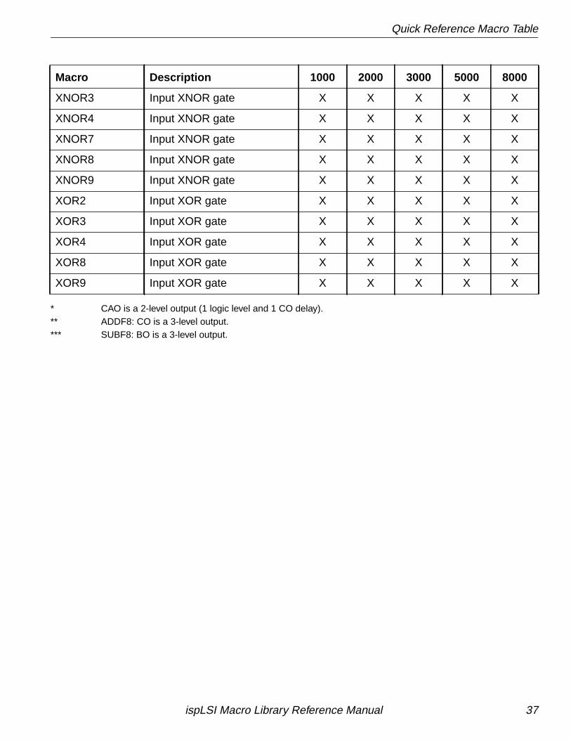
XNOR2 Input XNOR gate X X X X X
Macro Description 1000 2000 3000 5000 8000
ispLSI Macro Library Reference Manual 36
Quick Reference Macro Table
* CAO is a 2-level output (1 logic level and 1 CO delay).** ADDF8: CO is a 3-level output.*** SUBF8: BO is a 3-level output.
XNOR3 Input XNOR gate X X X X X
XNOR4 Input XNOR gate X X X X X
XNOR7 Input XNOR gate X X X X X
XNOR8 Input XNOR gate X X X X X
XNOR9 Input XNOR gate X X X X X
XOR2 Input XOR gate X X X X X
XOR3 Input XOR gate X X X X X
XOR4 Input XOR gate X X X X X
XOR8 Input XOR gate X X X X X
XOR9 Input XOR gate X X X X X
Macro Description 1000 2000 3000 5000 8000
ispLSI Macro Library Reference Manual 37
Arithmetic Functions
This chapter contains information on the following macros:
■ Adders
■ Comparators
■ Multipliers
■ Propagate-Generate
■ Subtractors
ispLSI Macro Library Reference Manual 38
Adders
Adders
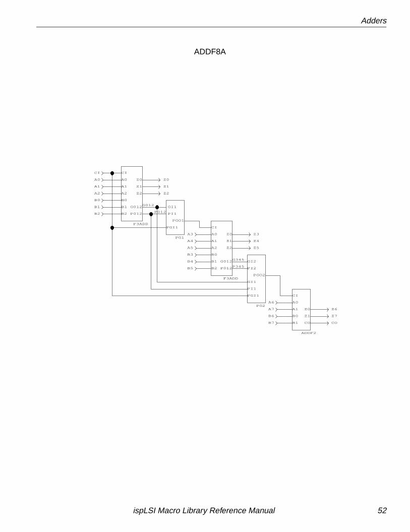
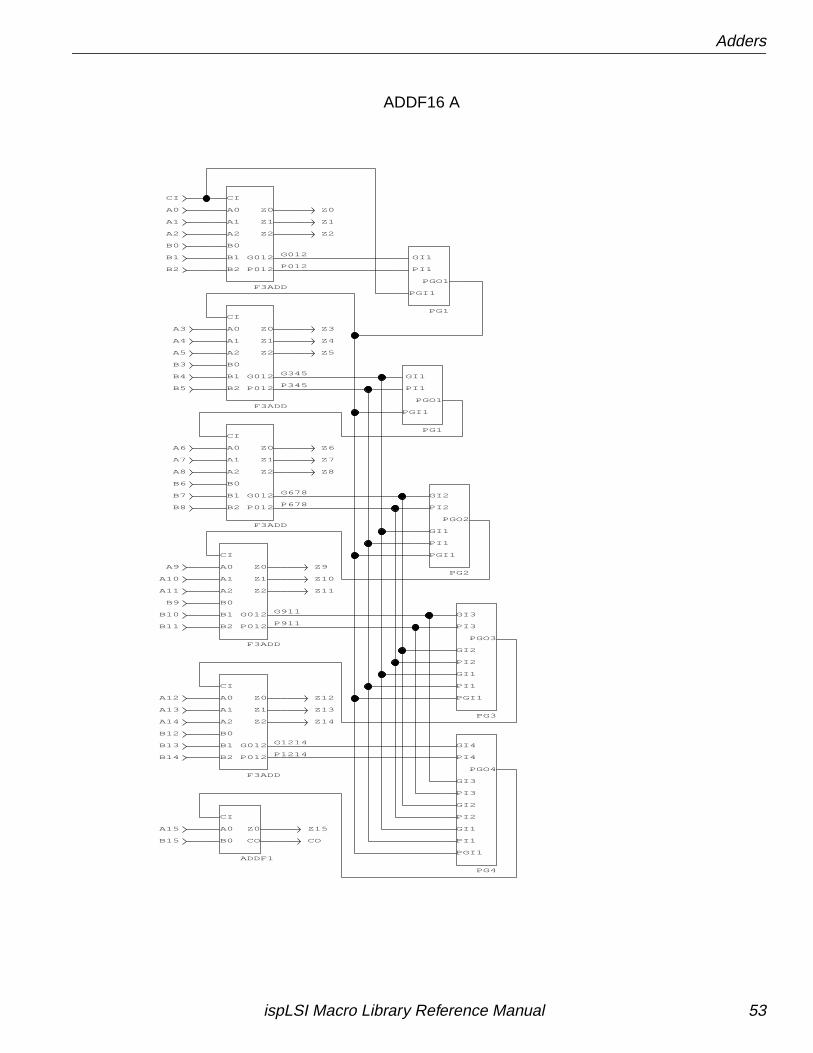
ADDF1, ADDF2, F3ADD, ADDF4,ADDF8, ADDF8A, and ADDF16A
Function:
ADDF1: 1-bit full adder.ADDF2: 2-bit full adder.F3ADD: 3-bit full adder with propagate-generate.ADDF4: 4-bit full adder.ADDF8: 8-bit full adder.ADDF8A: 8-bit full adder built with propagate-generate
submacros.ADDF16A: 16-bit full adder built with propagate-generate
submacros.
Availability:
ADDF1, ADDF2, F3ADD, ADDF4, ADDF8, ADDF8A, andADDF16A can be used with 1000, 2000, 3000, 5000, and8000 devices.
Additional symbols and schematics appear on thefollowing pages.
Type:
Soft: ADDF1, ADDF2, F3ADD, ADDF8A, ADDF16AHard: ADDF4, ADDF8
ADDF1
ADDF2
ADDF4
Z0
CO
A0
B0
CI
CO
Z1
Z0A1
CI
B1
B0
A0
Z1
Z0
Z2
Z3
CO
CI
A2
A3
B0
B1
B2
B3
A1
A0
F3ADD
CI
A0
A1
A2
B0
B1
B2
Z0
Z1
Z2
G012
P012
Z5
Z4
Z6
Z7
CO
Z1
Z0
Z2
Z3
ADDF8
A4
A5
A6
A7
B0
B1
B2
B3
B4
B5
B6
B7
A0
A1
A2
A3
CI
ispLSI Macro Library Reference Manual 39
Adders
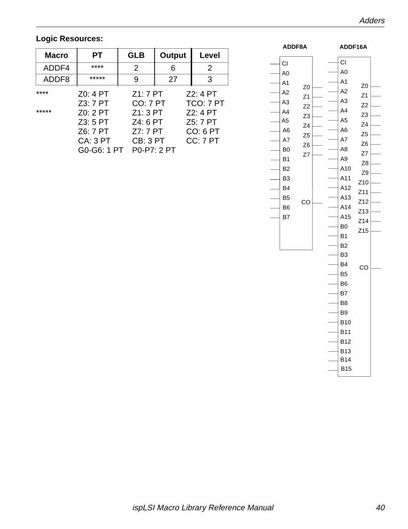
Logic Resources:
**** Z0: 4 PT Z1: 7 PT Z2: 4 PTZ3: 7 PT CO: 7 PT TCO: 7 PT
***** Z0: 2 PT Z1: 3 PT Z2: 4 PTZ3: 5 PT Z4: 6 PT Z5: 7 PTZ6: 7 PT Z7: 7 PT CO: 6 PTCA: 3 PT CB: 3 PT CC: 7 PTG0-G6: 1 PT P0-P7: 2 PT
Macro PT GLB Output Level
ADDF4 **** 2 6 2ADDF8 ***** 9 27 3
ADDF16A
CI
A0
A1
A2
A3
A4
A5
A12
A6
A7
A8
A9
A10
A11
Z0
Z1
Z2
Z3
Z4
Z5
Z6
A15
A13
A14
Z7
CO
B0
B1
B2
B3
B4
B5
B6
B11
B7
B8
B9
B10
B14
B12
B13
B15
Z8
Z9
Z10
Z11
Z12
Z13
Z14
Z15
ADDF8A
C1A0A1A2A3A4A5
B4
A6A7B0B1B2B3
Z0Z1Z2Z3Z4Z5Z6
B7
B5B6
Z7
C1
CI
A0
A1
A2
A3
A4A5
B4
A6
A7
B0
B1
B2
B3
Z0
Z1
Z2
Z3
Z4
Z5
Z6
B7
B5
B6
Z7
CO
ispLSI Macro Library Reference Manual 40
Adders
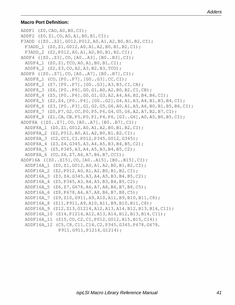
Macro Port Definition:
ADDF1 (Z0,CAO,A0,B0,CI);ADDF2 (Z0,Z1,CO,A0,A1,B0,B1,CI);F3ADD ([Z0..Z2],G012,P012,A0,A1,A2,B0,B1,B2,CI);
F3ADD_1 (Z0,Z1,G012,A0,A1,A2,B0,B1,B2,CI);F3ADD_2 (Z2,P012,A0,A1,A2,B0,B1,B2,CI);
ADDF4 ([Z0..Z3],CO,[A0..A3],[B0..B3],CI);ADDF4_1 (Z0,Z1,TCO,A0,A1,B0,B1,CI);ADDF4_2 (Z2,Z3,CO,A2,A3,B2,B3,TCO);
ADDF8 ([Z0..Z7],CO,[A0..A7],[B0..B7],CI);ADDF8_1 (CO,[P0..P7],[G0..G3],CC,CI);ADDF8_2 (Z7,[P0..P7],[G0..G3],A3,B3,CI,CA);ADDF8_3 (Z6,[P0..P6],G0,G1,A0,A2,B0,B2,CI,CB);ADDF8_4 (Z5,[P0..P6],G0,G1,G3,A2,A4,A6,B2,B4,B6,CI);ADDF8_5 (Z2,Z4,[P0..P4],[G0..G2],G4,A1,A3,A4,B1,B3,B4,CI);ADDF8_6 (Z3,[P0..P3],G1,G2,G5,G6,A0,A1,A5,A6,B0,B1,B5,B6,CI);ADDF8_7 (Z0,P7,G2,CC,P0,P5,P6,G4,G5,G6,A2,A7,B2,B7,CI);ADDF8_8 (Z1,CA,CB,P5,P0,P1,P4,P6,[G3..G6],A0,A5,B0,B5,CI);
ADDF8A ([Z0..Z7],CO,[A0..A7],[B0..B7],CI);ADDF8A_1 (Z0,Z1,G012,A0,A1,A2,B0,B1,B2,CI);ADDF8A_2 (Z2,P012,A0,A1,A2,B0,B1,B2,CI);ADDF8A_3 (C2,CCI,CI,P012,P345,G012,G345);ADDF8A_4 (Z3,Z4,G345,A3,A4,A5,B3,B4,B5,C2);ADDF8A_5 (Z5,P345,A3,A4,A5,B3,B4,B5,C2);ADDF8A_6 (CO,Z6,Z7,A6,A7,B6,B7,CCI);
ADDF16A ([Z0..Z15],CO,[A0..A15],[B0..B15],CI);ADDF16A_1 (Z0,Z1,G012,A0,A1,A2,B0,B1,B2,CI);ADDF16A_2 (Z2,P012,A0,A1,A2,B0,B1,B2,CI);ADDF16A_3 (Z3,Z4,G345,A3,A4,A5,B3,B4,B5,C2);ADDF16A_4 (Z5,P345,A3,A4,A5,B3,B4,B5,C2);ADDF16A_5 (Z6,Z7,G678,A6,A7,A8,B6,B7,B8,C5);ADDF16A_6 (Z8,P678,A6,A7,A8,B6,B7,B8,C5);ADDF16A_7 (Z9,Z10,G911,A9,A10,A11,B9,B10,B11,C8);ADDF16A_8 (Z11,P911,A9,A10,A11,B9,B10,B11,C8);ADDF16A_9 (Z12,Z13,G1214,A12,A13,A14,B12,B13,B14,C11);ADDF16A_10 (Z14,P1214,A12,A13,A14,B12,B13,B14,C11);ADDF16A_11 (Z15,CO,C2,CI,P012,G012,A15,B15,C14);ADDF16A_12 (C5,C8,C11,C14,C2,P345,G345,P678,G678,
P911,G911,P1214,G1214);
ispLSI Macro Library Reference Manual 41
Adders
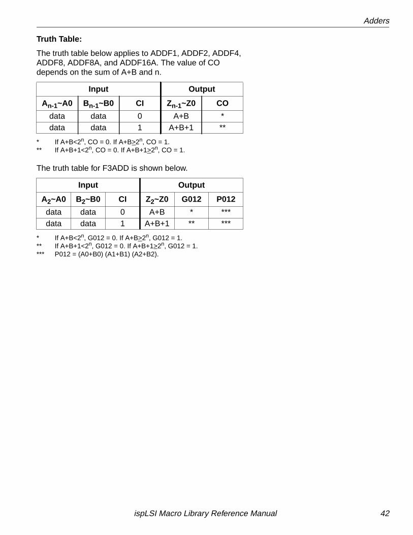
Truth Table:
The truth table below applies to ADDF1, ADDF2, ADDF4,ADDF8, ADDF8A, and ADDF16A. The value of COdepends on the sum of A+B and n.
* If A+B<2n, CO = 0. If A+B>2n, CO = 1.** If A+B+1<2n, CO = 0. If A+B+1>2n, CO = 1.
The truth table for F3ADD is shown below.
* If A+B<2n, G012 = 0. If A+B>2n, G012 = 1.** If A+B+1<2n, G012 = 0. If A+B+1>2n, G012 = 1.*** P012 = (A0+B0) (A1+B1) (A2+B2).
Input Output
An-1~A0 Bn-1~B0 CI Zn-1~Z0 CO
data data 0 A+B *data data 1 A+B+1 **
Input Output
A2~A0 B2~B0 CI Z2~Z0 G012 P012
data data 0 A+B * ***data data 1 A+B+1 ** ***
ispLSI Macro Library Reference Manual 42
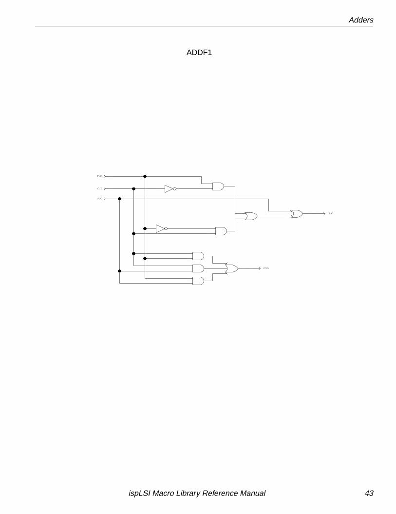
Adders
CI
B0
A0
Z0
CO
ADDF1
ispLSI Macro Library Reference Manual 43
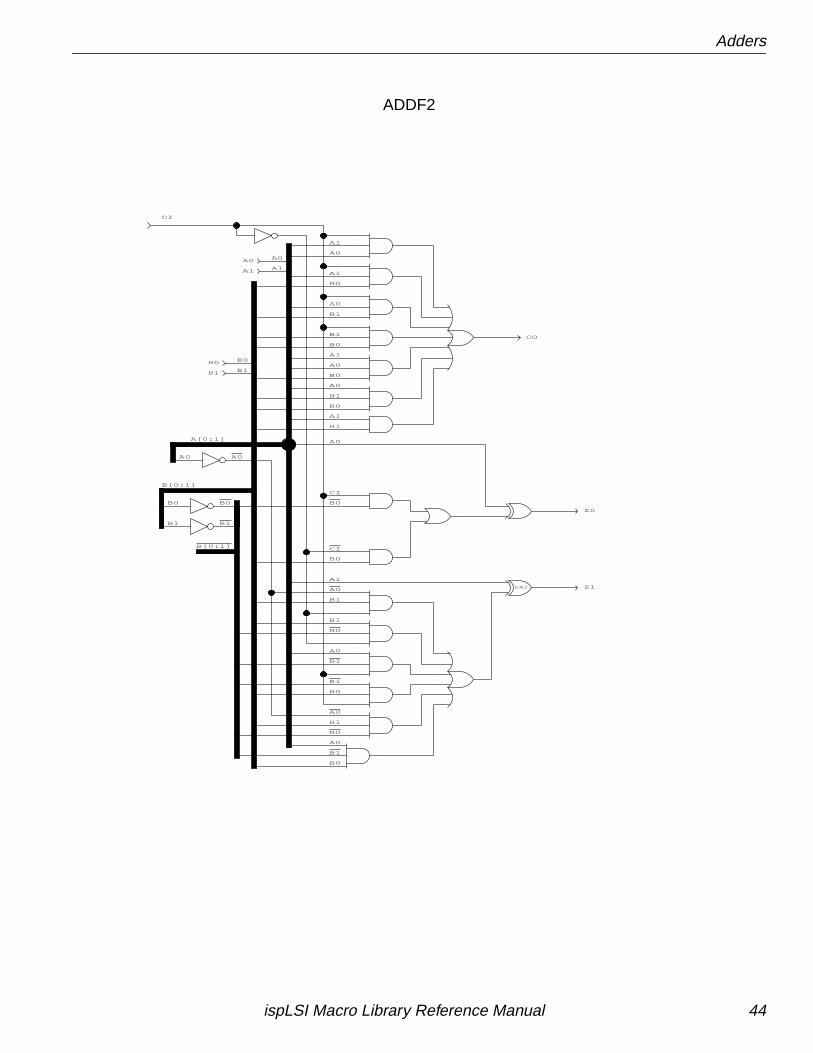
Adders
CI
CI
Z0
Z1
CO
B0
B1
A1
A0
LX2
B0
B1
B1
B0
B0
B1B0
B1
B0
B1
B0
B1
B[0:1]
B0
B1
B1
B0
B1
B0
A0
A0
A0
B0
B1
B[0:1]
B1
B0
B0
B1
B1
B0
A0
A1
A0
A1A1
A1
A0
A0
A1
A0
A1
A0
A[0:1]
A0
A0
A0
CI
ADDF2
ispLSI Macro Library Reference Manual 44
Adders
CI
P012
CI
B1
B0
B2
B0
B2
B[0:2]
B1B1
B2
B2
B2
B1
B0
B1
B0
B0
B1
B0
B1
B1
B0
B0
B0
B2
B1
B1
A1
A0
B0
A2
B2
Z0LX2
LX2 Z1
G012
B0
B1
B2
B[0:2]
B1
B0
B1
B0
B0
B1
B0
B1
B2
A1
A2
A0
A[0:2]
A1
A0
A2
A0
A1
A2
A2
A2
A0
A1
A0
A1
A2
A0
A1
A0
A0
A0
A1
A0
A1
A2
A1
A0
A0
A0
A2
A[0:2]
F3ADD.1
ispLSI Macro Library Reference Manual 45
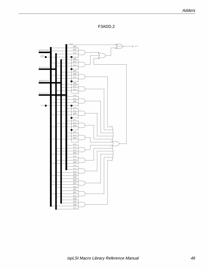
Adders
A[0:1]
A0
A0
A1
A0
A1
A0
A1
A1
CI
CI
B[0:2]
B0
B0
B0
B1
B1
B2
B2
B2
B2
B2
B2
B2
B0
B1
B1
A[0:2]
A1
A0
A1
A0
A1
A0
A1
A0
A2
B[0:2]
B2
B2
B2
B2
B2
B0
B1
B1
B0
B0
B1
B1
B0
B2
B2
LX2 Z2
F3ADD.2
ispLSI Macro Library Reference Manual 46
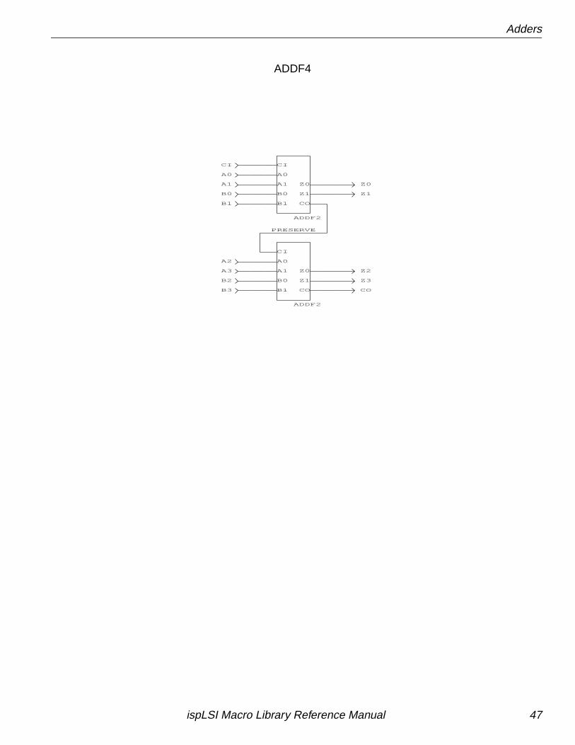
Adders
CI
B3
B2
A3
A2
CO
Z3
Z2
Z0
Z1
A0
A1
B0
B1
PRESERVE
A0
B0
B1
CI
A1
ADDF2
Z0
Z1
CO
A0
B0
B1
CI
A1
ADDF2
Z0
Z1
CO
ADDF4
ispLSI Macro Library Reference Manual 47
Adders
G7
PRESERVE
G6
PRESERVE
G5
PRESERVE
G4
PRESERVE
G3
PRESERVE
G2
PRESERVE
G1
PRESERVE
G0
PRESERVE
P7
PRESERVE
P6
PRESERVE
P4
PRESERVE
PRESERVE
P3
PRESERVE
P2
P1
PRESERVE
P0
PRESERVEB0
A0
A3
B3
A2
B2
A1
B1
B4
A4
B5
A5
B6
A6
B7
A7
P5
PRESERVE
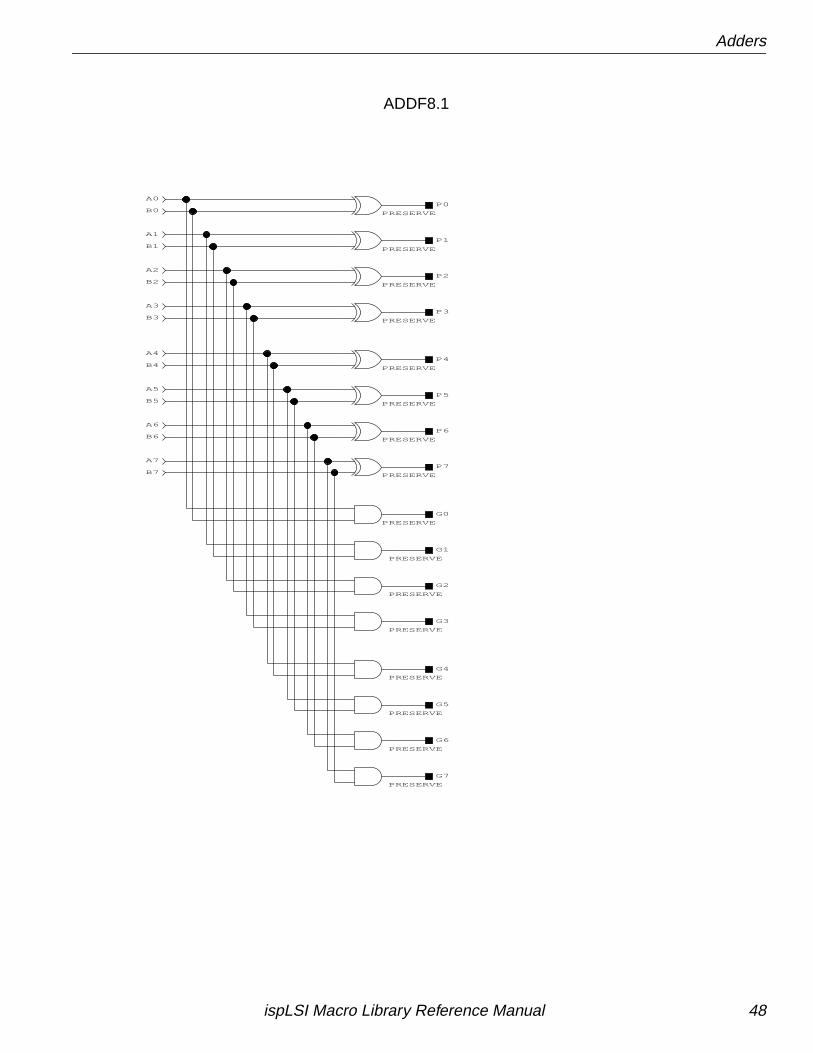
ADDF8.1
ispLSI Macro Library Reference Manual 48
Adders
Z5
P1
P2
G1
G0
P0
CI
Z2
G4
CO
P7
G7
G6
P6
G5
P5
G4
G3
P4
G2
P3
P2
G1
P1
G0
P0
CI
CI
P0
G0
P1
G1
P2
G2
P3
G3
P4
P5
LX2
LX2
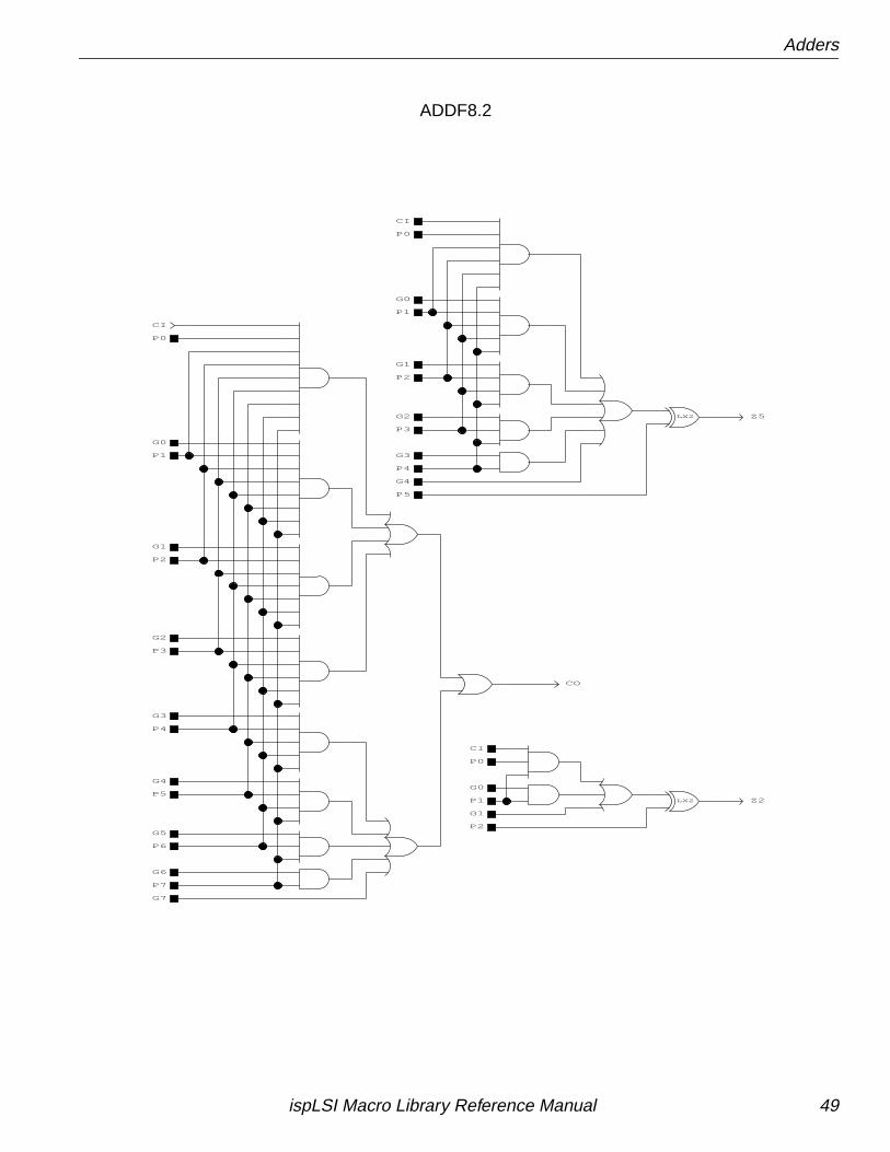
ADDF8.2
ispLSI Macro Library Reference Manual 49
Adders
P0
Z0
P1
Z1
P7
G6
P6
G5
P5
G4
P4
G3
P3
G2
P2
G1
G0
Z7
CI
LX2
LX2
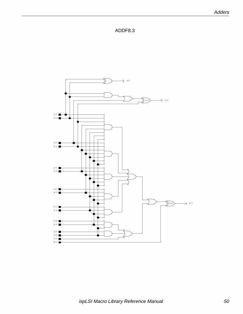
ADDF8.3
ispLSI Macro Library Reference Manual 50
Adders
Z4
P3
G2
Z3
G3
P4
Z6
P6
G5
P1
G0
P0
P5
G4
G3
P4
G2
P3
P2
G1
CI
P0
G0
P1
G1
P2
G2
P3
P2
G1
P1
G0
P0
CI
CI
LX2
LX2
LX2
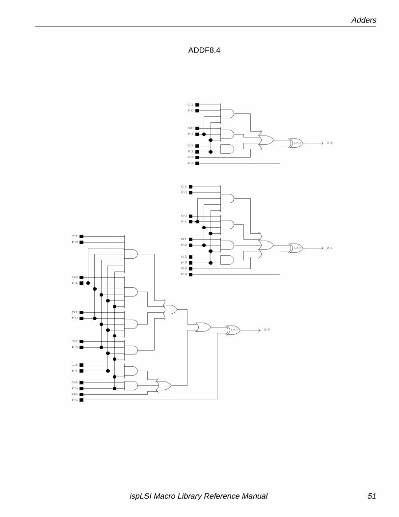
ADDF8.4
ispLSI Macro Library Reference Manual 51
Adders
CI
A1
A2
B0
B1
B2
Z1
Z2
Z0A0
Z3
Z4
Z5
B5
B4
B3
A5
A4
A3
G345
P345
P012
G012
A6
A7
B6
B7
Z6
Z7
CO
F3ADD
Z2
Z1
Z0
G012
P012
A0
A1
B2
B1
B0
A2
CI
PGO1
PG1
PGI1
PI1
GI1
F3ADD
Z2
Z1
Z0
G012
P012
A0
A1
B2
B1
B0
A2
CI
PGO2
GI1
PI1
PGI1
PG2
GI2
PI2
A0
B0
B1
CI
A1
ADDF2
Z0
Z1
CO
ADDF8A
ispLSI Macro Library Reference Manual 52
Adders
P012
CI
G678
P678
P911
B15
A15
CO
Z15
P345
G345
G911
Z11
Z10
Z9A9
A10
A11
B9
B10
B11
A12
B13
B14
Z12
Z7
Z6A6
A7
B8
B7
B6
A8 Z8
Z5
A4
A3
A5
B3
B4
B5
Z3
Z4
A1
A2
B0
B1
B2
Z1
Z2
Z0A0
Z13
B12
A14
A13
Z14
G1214
P1214
G012
F3ADD
Z2
Z1
Z0
G012
P012
A0
A1
B2
B1
B0
A2
CI
F3ADD
Z2
Z1
Z0
G012
P012
A0
A1
B2
B1
B0
A2
CI
F3ADD
Z2
Z1
Z0
G012
P012
A0
A1
B2
B1
B0
A2
CI
F3ADD
Z2
Z1
Z0
G012
P012
A0
A1
B2
B1
B0
A2
CI
F3ADD
Z2
Z1
Z0
G012
P012
A0
A1
B2
B1
B0
A2
CI
ADDF1
Z0
CO
A0
B0
CI
PGO1
PG1
PGI1
PI1
GI1
PGO1
PG1
PGI1
PI1
GI1
PGO2
GI1
PI1
PGI1
PG2
GI2
PI2
PGO3
PI3
GI3
PI2
GI2
PI1
PGI1
GI1
PG3
PGO4
PI4
GI4
GI3
PG4
GI1
PGI1
PI1
PI2
PI3
GI2
ADDF16 A
ispLSI Macro Library Reference Manual 53
Adders
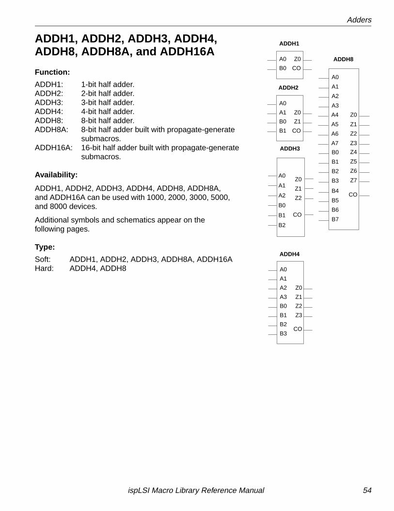
ADDH1, ADDH2, ADDH3, ADDH4,ADDH8, ADDH8A, and ADDH16A
Function:
ADDH1: 1-bit half adder.ADDH2: 2-bit half adder.ADDH3: 3-bit half adder.ADDH4: 4-bit half adder.ADDH8: 8-bit half adder.ADDH8A: 8-bit half adder built with propagate-generate
submacros.ADDH16A: 16-bit half adder built with propagate-generate
submacros.
Availability:
ADDH1, ADDH2, ADDH3, ADDH4, ADDH8, ADDH8A,and ADDH16A can be used with 1000, 2000, 3000, 5000,and 8000 devices.
Additional symbols and schematics appear on thefollowing pages.
Type:
Soft: ADDH1, ADDH2, ADDH3, ADDH8A, ADDH16AHard: ADDH4, ADDH8
ADDH1
ADDH2
B0
A0 Z0
CO
CO
Z1
Z0A1
B1
B0
A0
ADDH4
Z1
Z0
Z2
Z3
CO
A2
A3
B0
B1
B2
B3
A1
A0
ADDH3
A0
A1
A2
B0
B1
B2
CO
Z1
Z2
Z0
Z5
Z4
Z6
Z7
CO
Z1
Z0
Z2
Z3
ADDH8
A4
A5
A6
A7
B0
B1
B2
B3
B4
B5
B6
B7
A0
A1
A2
A3
ispLSI Macro Library Reference Manual 54
Adders
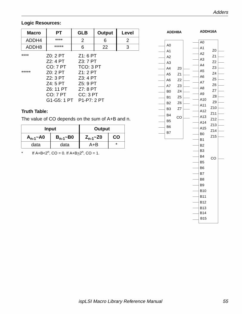
Logic Resources:
**** Z0: 2 PT Z1: 6 PTZ2: 4 PT Z3: 7 PTCO: 7 PT TCO: 3 PT
***** Z0: 2 PT Z1: 2 PTZ2: 3 PT Z3: 4 PTZ4: 5 PT Z5: 9 PTZ6: 11 PT Z7: 8 PTCO: 7 PT CC: 3 PTG1-G5: 1 PT P1-P7: 2 PT
Truth Table:
The value of CO depends on the sum of A+B and n.
* If A+B<2n, CO = 0. If A+B>2n, CO = 1.
Macro PT GLB Output Level
ADDH4 **** 2 6 2ADDH8 ***** 6 22 3
Input Output
An-1~A0 Bn-1~B0 Zn-1~Z0 CO
data data A+B *
A0
A1
A2
A3
A4
A5
A12
A6
A7
A8
A9
A10
A11
Z0
Z1
Z2
Z3
Z4
Z5
Z6
A15
A13
A14
Z7
CO
B0
B1
B2
B3
B4
B5
B6
B11
B7
B8
B9
B10
B14
B12
B13
B15
Z8
Z9
Z10
Z11
Z12
Z13
Z14
Z15
ADDH16AADDH8A
Z5
Z4
Z6
Z7
CO
Z1
Z0
Z2
Z3
A4
A5
A6
A7
B0
B1
B2
B3
B4
B5
B6
B7
A0
A1
A2
A3
ispLSI Macro Library Reference Manual 55
Adders
Macro Port Definition:
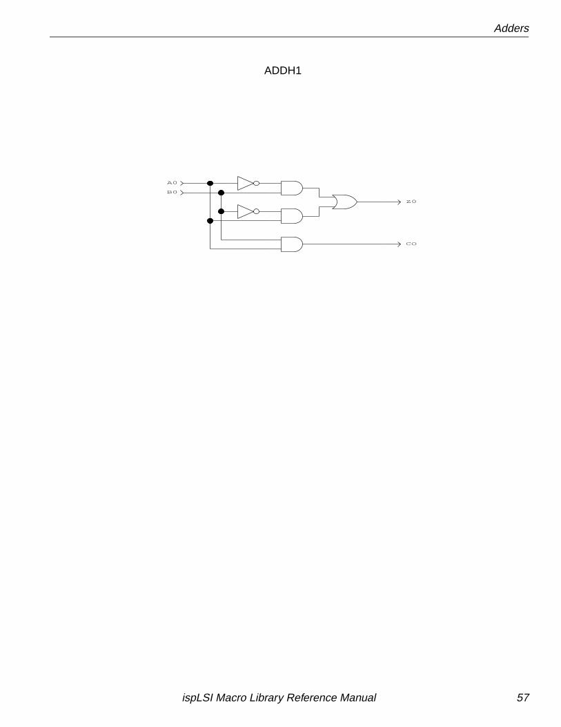
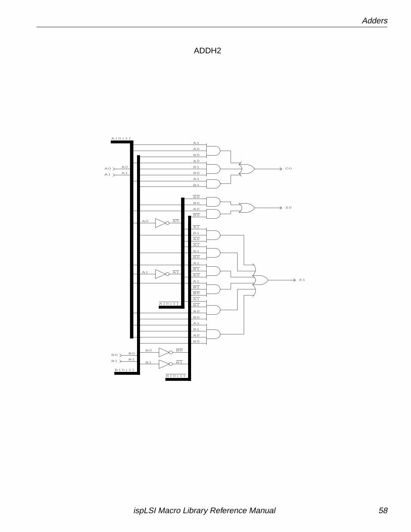
ADDH1 (Z0,CO,A0,B0);ADDH2 (Z0,Z1,CO,A0,A1,B0,B1);ADDH3 ([Z0..Z2],CO,A0,A1,A2,B0,B1,B2);
ADDH3_1 (Z0,A0,B0);ADDH3_2 (Z1,Z2,CO,A0,A1,A2,B0,B1,B2);
ADDH4 ([Z0..Z3],CO,[A0..A3],[B0..B3]);ADDH4_1 (Z0,Z1,TCO,A0,A1,B0,B1);ADDH4_2 (Z2,Z3,CO,A2,A3,B2,B3,TCO);
ADDH8 ([Z0..Z7],CO,[A0..A7],[B0..B7]);ADDH8_1 (CO,Z1,Z3,[P1..P7],[G1..G5],A0,B0,CC);ADDH8_2 (Z0,Z2,Z4,Z7,[P1..P7],[G1..G5],A0,A6,B0,B6);ADDH8_3 (Z6,G5,G4,P4,[P1..P3],P5,P6,[G1..G3],A0,A4,A5,B0,B4,B5);ADDH8_4 (Z5,G3,P3,G1,P1,P2,P4,P5,G2,G4,A0,A1,A3,B0,B1,B3);ADDH8_5 (G2,P2,P1,A1,A2,B1,B2);ADDH8_6 (P7,P6,P5,CC,[A5..A7],[B5..B7]);
ADDH8A ([Z0..Z7],CO,[A0..A7],[B0..B7]);ADDH8A_1 (Z0,A0,B0,C2,CCI,P345,G345);ADDH8A_2 (Z1,Z2,C2,A0,A1,A2,B0,B1,B2);ADDH8A_3 (Z3,Z4,G345,A3,A4,A5,B3,B4,B5,C2);ADDH8A_4 (Z5,P345,A3,A4,A5,B3,B4,B5,C2);ADDH8A_5 (Z6,Z7,CO,A6,A7,B6,B7,CCI);
ADDH16A ([Z0..Z15],CO,[A0..A15],[B0..B15]);ADDH16A_1 (Z0,Z15,CO,A0,A15,B0,B15,C14);ADDH16A_2 (Z1,Z2,C2,A0,A1,A2,B0,B1,B2);ADDH16A_3 (Z3,Z4,G345,A3,A4,A5,B3,B4,B5,C2);ADDH16A_4 (Z5,P345,A3,A4,A5,B3,B4,B5,C2);ADDH16A_5 (Z6,Z7,G678,A6,A7,A8,B6,B7,B8,C5);ADDH16A_6 (Z8,P678,A6,A7,A8,B6,B7,B8,C5);ADDH16A_7 (Z9,Z10,G911,A9,A10,A11,B9,B10,B11,C8);ADDH16A_8 (Z11,P911,A9,A10,A11,B9,B10,B11,C8);ADDH16A_9 (Z12,Z13,G1214,A12,A13,A14,B12,B13,B14,C11);ADDH16A_10 (Z14,P1214,A12,A13,A14,B12,B13,B14,C11);ADDH16A_11 (C5,C8,C11,C14,C2,P345,G345,P678,G678,P911,G911,
P1214,G1214);
ispLSI Macro Library Reference Manual 56
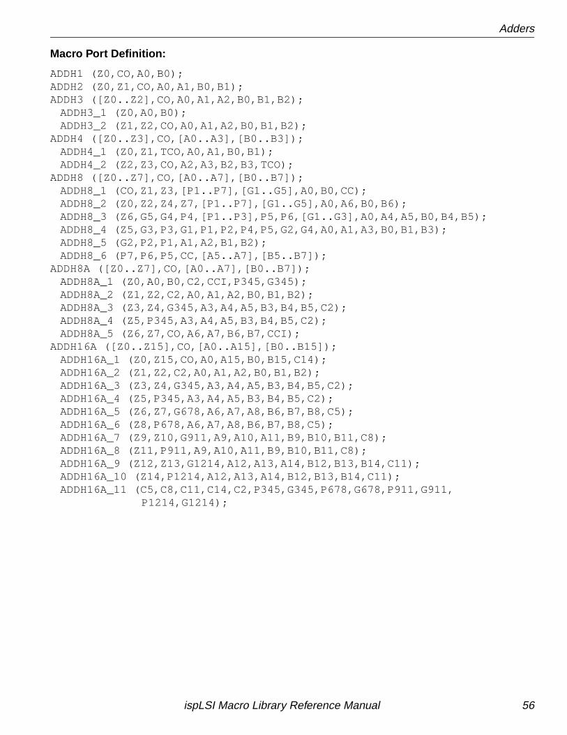
Adders
Z0
CO
B0
A0
ADDH1
ispLSI Macro Library Reference Manual 57
Adders
A0
A1
A0
A0
A0
A[0:1]
A1
A1
A1
A0
A1
A1
A0
A1
A0
A0
A1
A[0:1]
A1
A0
A1
A0
A0
A1
B0
B1
B[0:1]
B1
B0
B1
B0
B1
B0
B1
B0
B1
B0
B1
B0B0
B1
Z1
Z0
COA0
A1
B[0:1]
B0
B1
B0
B0
B1
B1
B1
B0
ADDH2
ispLSI Macro Library Reference Manual 58
Adders
A2
A1
A0
B2
B1
B0
B0
B[0:2]
B1
B0
B1
B2
A[0:1]
A1
A0
A0
Z1LX2
Z0LX2
CO
B1
B1
B2
B1
B0
B2
B2
B0
B2
B1
B0
B1
B0
B0
B1
B0
B0
B1
B2
B[0:2]
B0
B2
B1
A1
A0
A0
A1
A0
A1
A0
A1
A0
A2
A2
A2
A2
A1
A0
A[0:2]
A0
A1
A0
A2
A1
ADDH3.1
ispLSI Macro Library Reference Manual 59
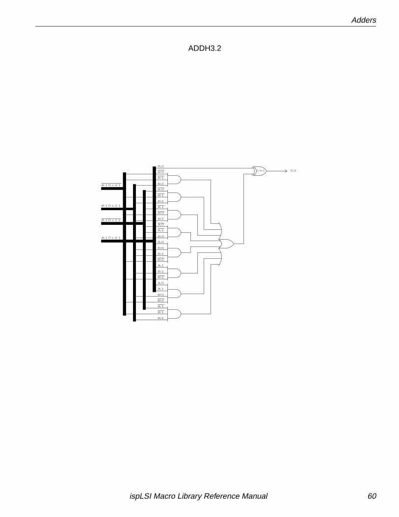
Adders
LX2 Z2
B2
B1
B2
B0
B[0:2]
B1
B0
B2
B1
B1
B2
B0
B0
B2
B2
B[0:2]
B2
B2
B1
A1
A1
A0
A[0:1]
A1
A0
A2
A0
A1
A0
A1
A[0:2]
ADDH3.2
ispLSI Macro Library Reference Manual 60
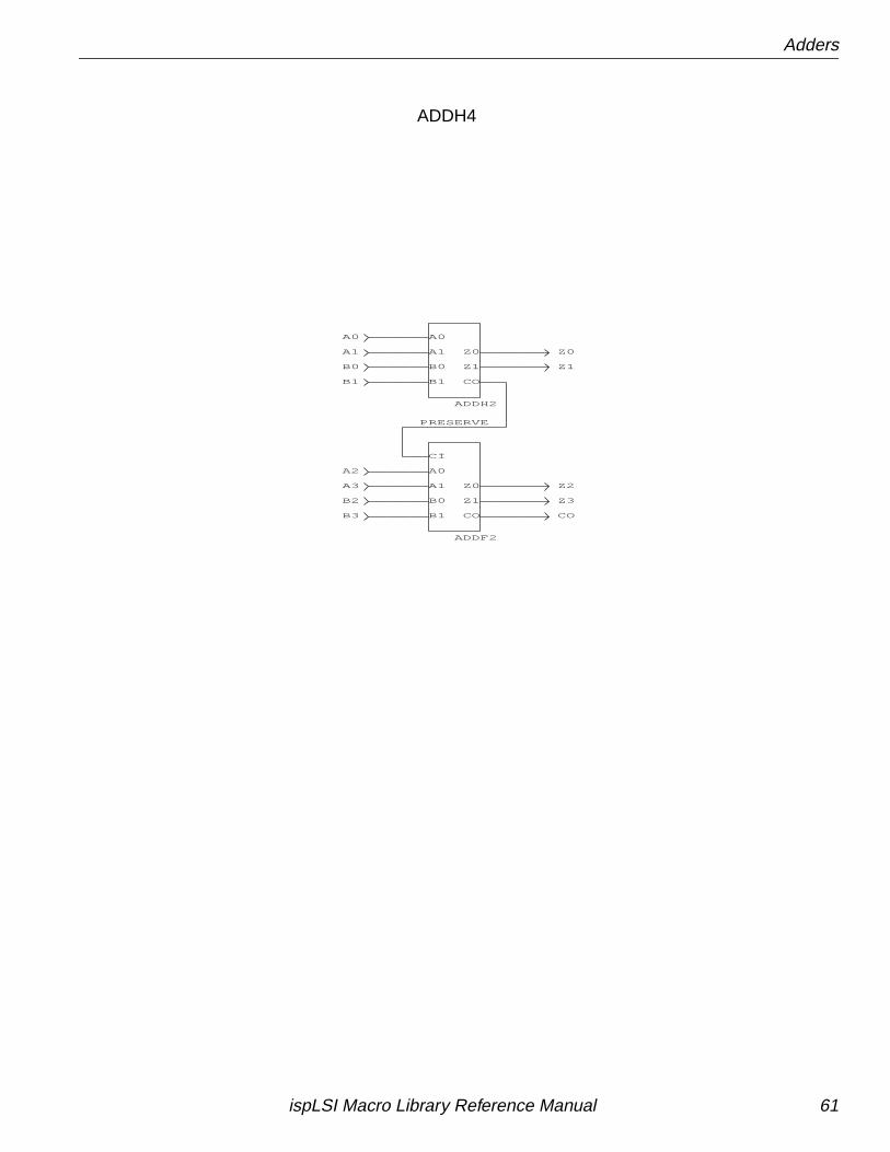
Adders
PRESERVE
A0
B0
B1
CI
A1
ADDF2
Z0
Z1
COB3
B2
A3
A2
CO
Z3
Z2
Z0
Z1
A0
A1
B0
B1
A0
B0
B1
A1 Z0
Z1
CO
ADDH2
ADDH4
ispLSI Macro Library Reference Manual 61
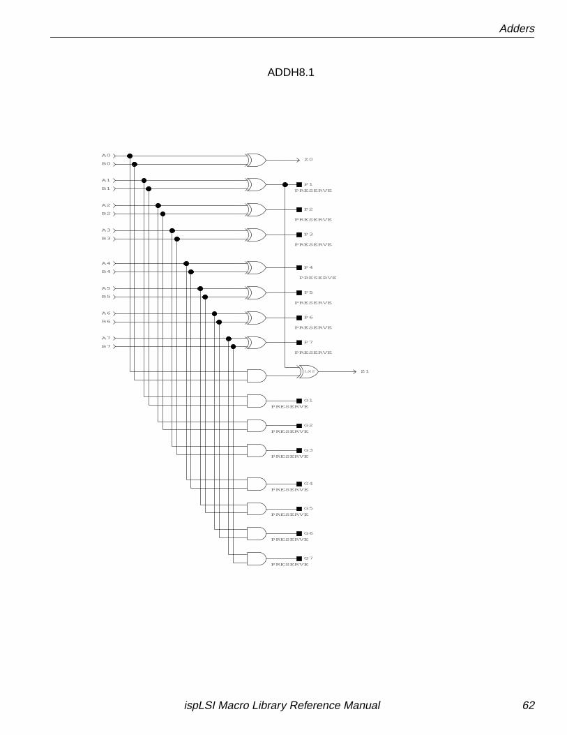
Adders
P1
PRESERVE
P2
PRESERVE
P3
PRESERVE
P4
PRESERVE
P5
PRESERVE
P6
PRESERVE
P7
PRESERVE
G1
PRESERVE
G2
PRESERVE
G3
PRESERVE
G7
PRESERVE
G6
PRESERVE
G5
PRESERVE
G4
PRESERVE
LX2
Z0B0
A0
A3
B3
A2
B2
A1
B1
B4
A4
B5
A5
B6
A6
B7
A7
Z1
ADDH8.1
ispLSI Macro Library Reference Manual 62
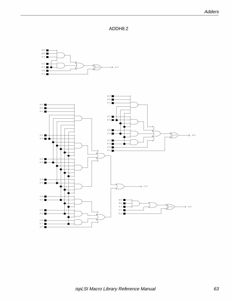
Adders
CO
P1
P7
P2
G1
P1
A0
B0
Z2
P1
B0
A0
P5
G4
P4
G3
P3
G2
P2
G1
G7
G6
P6
G5
P5
G4
P4
G3
P3
G2
P2
G1
B0
A0
Z5
Z3
B0
P1
P3
G2
P2
G1
A0
LX2
LX2
LX2
ADDH8.2
ispLSI Macro Library Reference Manual 63
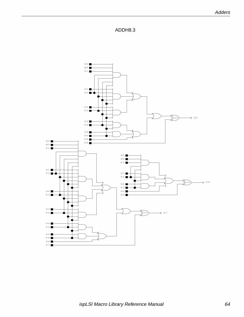
Adders
P1
G1
P2
G2
P3
G3
P4
G4
P5
G5
P6
B0
A0
Z6
A0
Z7
P7
P1
G1
P2
G2
P3
G3
P4
G4
P5
G5
P6
G6
B0
Z4
B0
P1
G1
P2
G2
P3
G3
P4
A0
LX2
LX2
LX2
ADDH8.3
ispLSI Macro Library Reference Manual 64
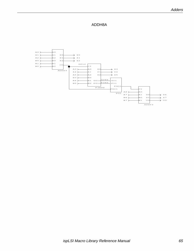
Adders
CO
Z7
Z6
B7
B6
A7
A6
P345
G345
A0
Z0
Z2
Z1
B2
B1
B0
A2
A1
Z5
A4
A3
A5
B3
B4
B5
Z3
Z4
G012
ADDH3
A0
A1
B2
B1
B0
A2
CO
Z2
Z0
Z1
F3ADD
Z2
Z1
Z0
G012
P012
A0
A1
B2
B1
B0
A2
CI
PGO1
PG1
PGI1
PI1
GI1
A0
B0
B1
CI
A1
ADDF2
Z0
Z1
CO
ADDH8A
ispLSI Macro Library Reference Manual 65
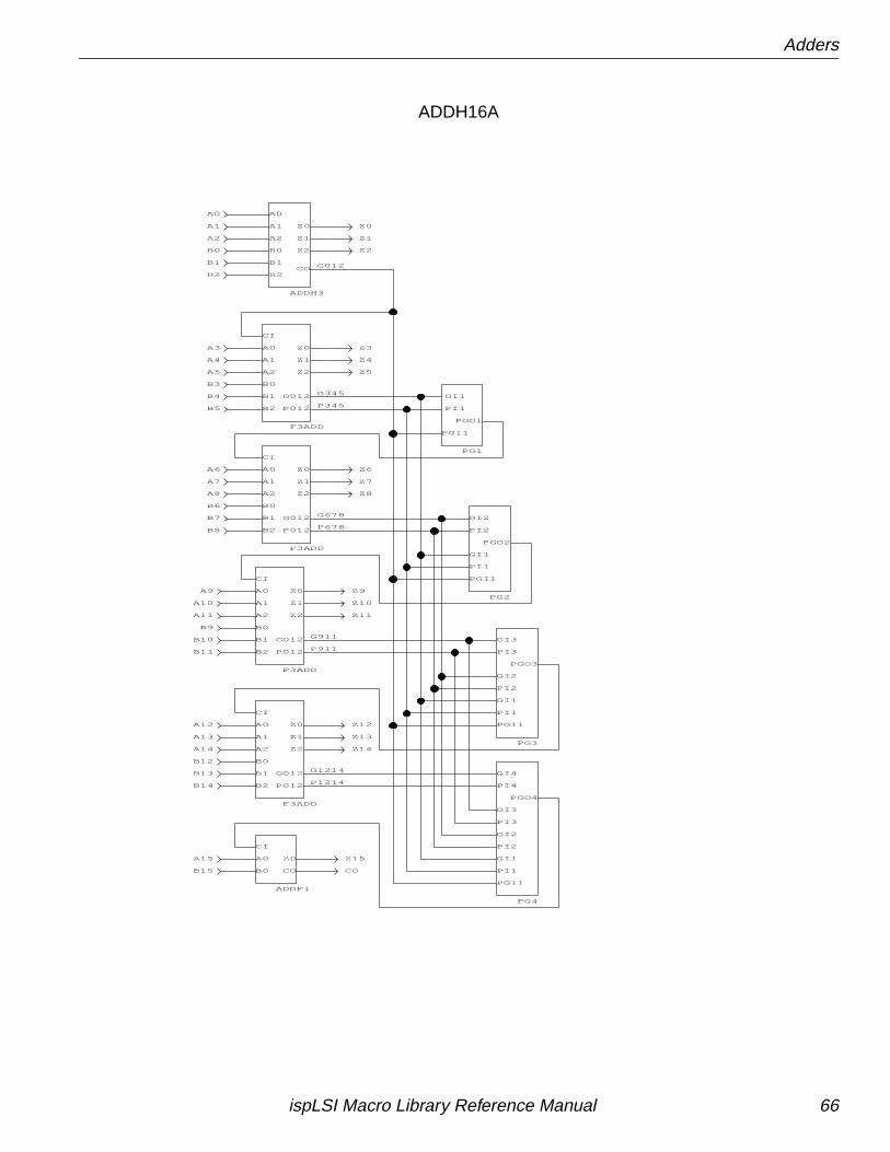
Adders
G678
P678
P911
B15
A15
CO
Z15
P345
G345
G911
Z11
Z10
Z9A9
A10
A11
B9
B10
B11
A12
B13
B14
Z12
Z7
Z6A6
A7
B8
B7
B6
A8 Z8
Z5
A4
A3
A5
B3
B4
B5
Z3
Z4
A1
A2
B0
B1
B2
Z1
Z2
Z0
A0
Z13
B12
A14
A13
Z14
G1214
P1214
G012
ADDH3
A0
A1
B2
B1
B0
A2
CO
Z2
Z0
Z1
F3ADD
Z2
Z1
Z0
G012
P012
A0
A1
B2
B1
B0
A2
CI
F3ADD
Z2
Z1
Z0
G012
P012
A0
A1
B2
B1
B0
A2
CI
F3ADD
Z2
Z1
Z0
G012
P012
A0
A1
B2
B1
B0
A2
CI
F3ADD
Z2
Z1
Z0
G012
P012
A0
A1
B2
B1
B0
A2
CI
ADDF1
Z0
CO
A0
B0
CI
PGO1
PG1
PGI1
PI1
GI1
PGO2
GI1
PI1
PGI1
PG2
GI2
PI2
PGO3
PI3
GI3
PI2
GI2
PI1
PGI1
GI1
PG3
PGO4
PI4
GI4
GI3
PG4
GI1
PGI1
PI1
PI2
PI3
GI2
ADDH16A
ispLSI Macro Library Reference Manual 66
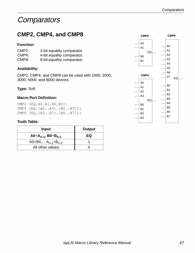
Comparators
Comparators
CMP2, CMP4, and CMP8
Function:
CMP2: 2-bit equality comparator.CMP4: 4-bit equality comparator.CMP8: 8-bit equality comparator.
Availability:
CMP2, CMP4, and CMP8 can be used with 1000, 2000,3000, 5000, and 8000 devices.
Type: Soft
Macro Port Definition:
CMP2 (EQ,A0,A1,B0,B1);CMP4 (EQ,[A0..A3],[B0..B3]);CMP8 (EQ,[A0..A7],[B0..B7]);
Truth Table:
Input Output
A0~An-1, B0~Bn-1 EQ
A0=B0,... An-1=Bn-1 1All other values 0
CMP2 CMP8
EQ
A1
B0
B1
A0
CMP4
EQ
A0
A1
A2
A3
B0
B1
B2
B3
EQA7
B4
B7
B6
B5
B3
B2
B1
B0
A6
A5
A4
A3
A2
A1
A0
ispLSI Macro Library Reference Manual 67
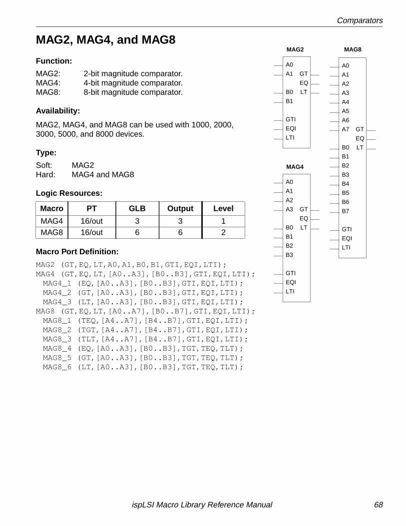
Comparators
MAG2, MAG4, and MAG8
Function:
MAG2: 2-bit magnitude comparator.MAG4: 4-bit magnitude comparator.MAG8: 8-bit magnitude comparator.
Availability:
MAG2, MAG4, and MAG8 can be used with 1000, 2000,3000, 5000, and 8000 devices.
Type:
Soft: MAG2Hard: MAG4 and MAG8
Logic Resources:
Macro Port Definition:
MAG2 (GT,EQ,LT,A0,A1,B0,B1,GTI,EQI,LTI);MAG4 (GT,EQ,LT,[A0..A3],[B0..B3],GTI,EQI,LTI);
MAG4_1 (EQ,[A0..A3],[B0..B3],GTI,EQI,LTI);MAG4_2 (GT,[A0..A3],[B0..B3],GTI,EQI,LTI);MAG4_3 (LT,[A0..A3],[B0..B3],GTI,EQI,LTI);
MAG8 (GT,EQ,LT,[A0..A7],[B0..B7],GTI,EQI,LTI);MAG8_1 (TEQ,[A4..A7],[B4..B7],GTI,EQI,LTI);MAG8_2 (TGT,[A4..A7],[B4..B7],GTI,EQI,LTI);MAG8_3 (TLT,[A4..A7],[B4..B7],GTI,EQI,LTI);MAG8_4 (EQ,[A0..A3],[B0..B3],TGT,TEQ,TLT);MAG8_5 (GT,[A0..A3],[B0..B3],TGT,TEQ,TLT);MAG8_6 (LT,[A0..A3],[B0..B3],TGT,TEQ,TLT);
Macro PT GLB Output Level
MAG4 16/out 3 3 1MAG8 16/out 6 6 2
MAG2
MAG4
A1
A0
GT
EQ
LT
LTI
EQI
GTI
B1
B0
A0
A1
A2
A3
B0
B1
B2
B3
GTI
EQI
LTI
LT
EQ
GT
MAG8
GT
EQ
LT
LTI
EQI
GTI
B7
B6
B5
B4
B3
B2
B1
B0
A7
A6
A5
A4
A3
A2
A1
A0
ispLSI Macro Library Reference Manual 68
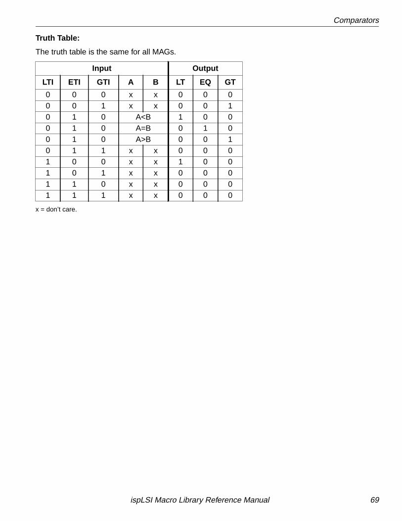
Comparators
Truth Table:
The truth table is the same for all MAGs.
x = don’t care.
Input Output
LTI ETI GTI A B LT EQ GT
0 0 0 x x 0 0 00 0 1 x x 0 0 10 1 0 A<B 1 0 00 1 0 A=B 0 1 00 1 0 A>B 0 0 10 1 1 x x 0 0 01 0 0 x x 1 0 01 0 1 x x 0 0 01 1 0 x x 0 0 01 1 1 x x 0 0 0
ispLSI Macro Library Reference Manual 69
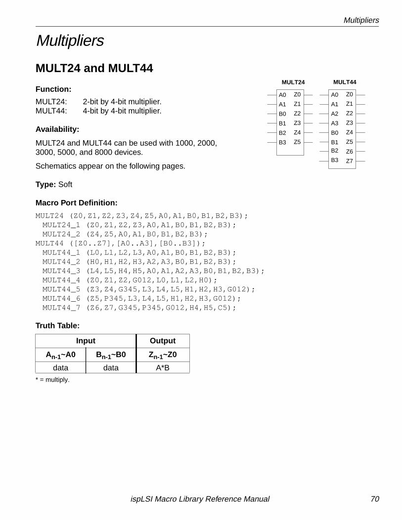
Multipliers
Multipliers
MULT24 and MULT44
Function:
MULT24: 2-bit by 4-bit multiplier.MULT44: 4-bit by 4-bit multiplier.
Availability:
MULT24 and MULT44 can be used with 1000, 2000,3000, 5000, and 8000 devices.
Schematics appear on the following pages.
Type: Soft
Macro Port Definition:
MULT24 (Z0,Z1,Z2,Z3,Z4,Z5,A0,A1,B0,B1,B2,B3);MULT24_1 (Z0,Z1,Z2,Z3,A0,A1,B0,B1,B2,B3);MULT24_2 (Z4,Z5,A0,A1,B0,B1,B2,B3);
MULT44 ([Z0..Z7],[A0..A3],[B0..B3]);MULT44_1 (L0,L1,L2,L3,A0,A1,B0,B1,B2,B3);MULT44_2 (H0,H1,H2,H3,A2,A3,B0,B1,B2,B3);MULT44_3 (L4,L5,H4,H5,A0,A1,A2,A3,B0,B1,B2,B3);MULT44_4 (Z0,Z1,Z2,G012,L0,L1,L2,H0);MULT44_5 (Z3,Z4,G345,L3,L4,L5,H1,H2,H3,G012);MULT44_6 (Z5,P345,L3,L4,L5,H1,H2,H3,G012);MULT44_7 (Z6,Z7,G345,P345,G012,H4,H5,C5);
Truth Table:
* = multiply.
Input Output
An-1~A0 Bn-1~B0 Zn-1~Z0
data data A*B
B3
A1
A0
MULT24 MULT44
B1
B0
B2
Z5
Z1
Z0
Z3
Z2
Z4
B1
A1
A0
A3
A2
B0
Z5
Z1
Z0
Z3
Z2
Z4
Z7
Z6B3
B2
ispLSI Macro Library Reference Manual 70
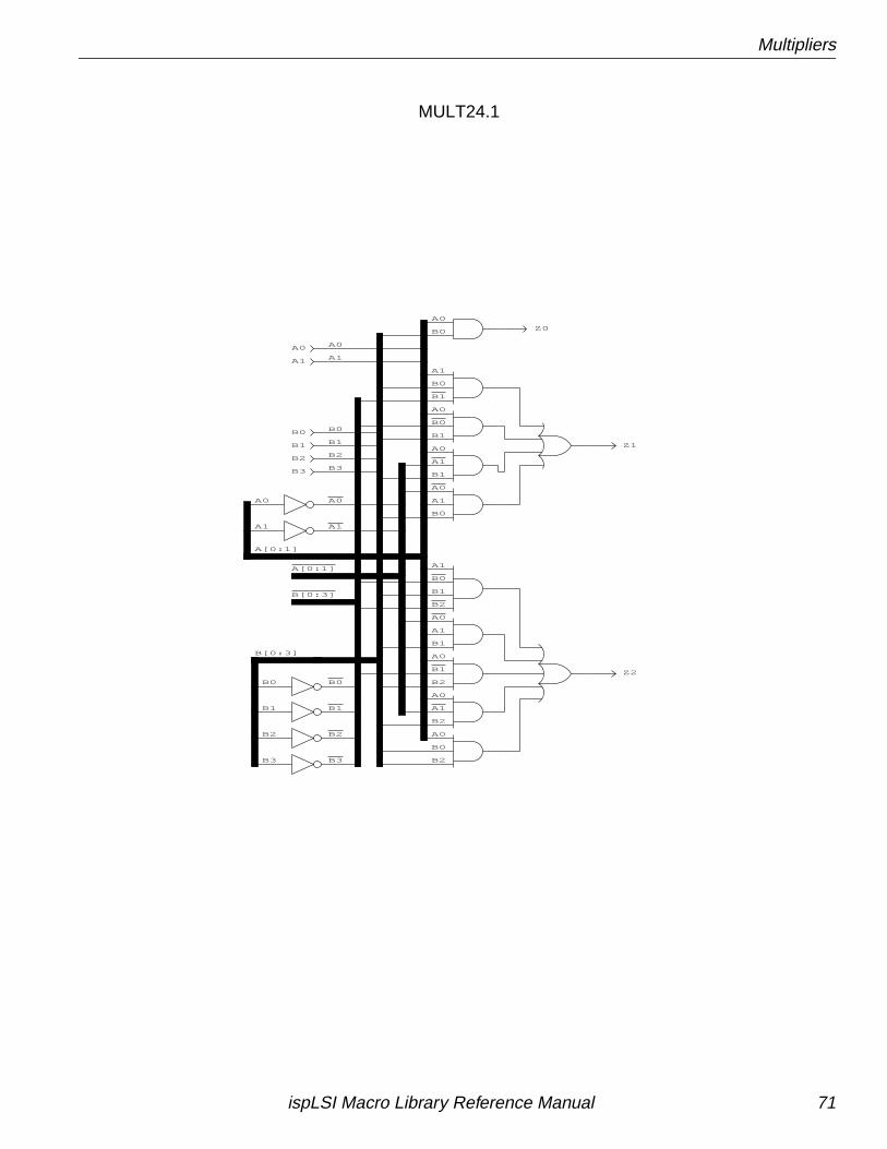
Multipliers
Z0
B3
B1
B1
B2
B0
B2
B2
B0
B1
B1
B0
B0
B0
B1
B2
B0
B[0:3]
B2
B3
B1
B[0:3]
B0
B1
B0
B1
B0
B3
B2
B1
B2
A[0:1]
A1
A0
A1
A0
A1
A0
A1
A1
A0
A0
A0
A1
A0
A0
A1
A1
A0
A0
A[0:1]
A1
A0
A0
A1
Z2
Z1
B0
B1
B2
B3
MULT24.1
ispLSI Macro Library Reference Manual 71
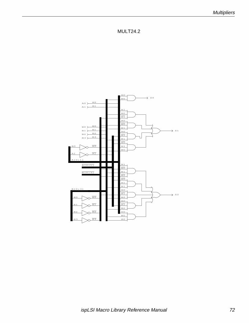
Multipliers
Z0
B3
B1
B1
B2
B0
B2
B2
B0
B1
B1
B0
B0
B0
B1
B2
B0
B[0:3]
B2
B3
B1
B[0:3]
B0
B1
B0
B1
B0
B3
B2
B1
B2
A[0:1]
A1
A0
A1
A0
A1
A0
A1
A1
A0
A0
A0
A1
A0
A0
A1
A1
A0
A0
A[0:1]
A1
A0
A0
A1
Z2
Z1
B0
B1
B2
B3
MULT24.2
ispLSI Macro Library Reference Manual 72
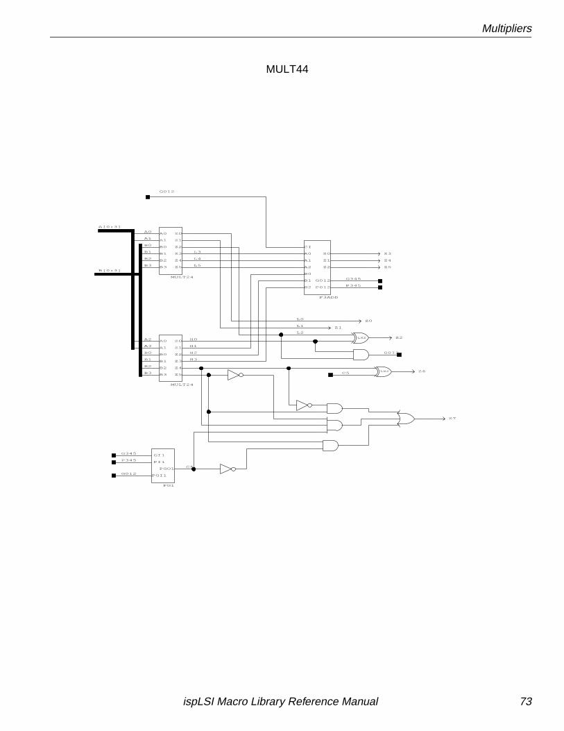
Multipliers
G012
H0
G012
L2
L0
L1
C5
Z7
C5
G012
P345
G345
PGO1
PG1
PGI1
PI1
GI1
Z1
P345
F3ADD
Z2
Z1
Z0
G012
P012
A0
A1
B2
B1
B0
A2
CI
G345
Z2
H2
H1
L5
L4
L3
Z6
Z5
Z4
Z3
Z0
A[0:3]
A0
A1
A2
A3
B[0:3]
B0
B1
B2
B3
B0
B1
B2
B3
A1
A0 Z0
Z1
Z2
Z3
Z4
Z5
MULT24
B0
B1
B2
B3
A1
A0 Z0
Z1
Z2
Z3
Z4
Z5
MULT24
B0
B1
B2
B3
LX2
LX2
H3
MULT44
ispLSI Macro Library Reference Manual 73
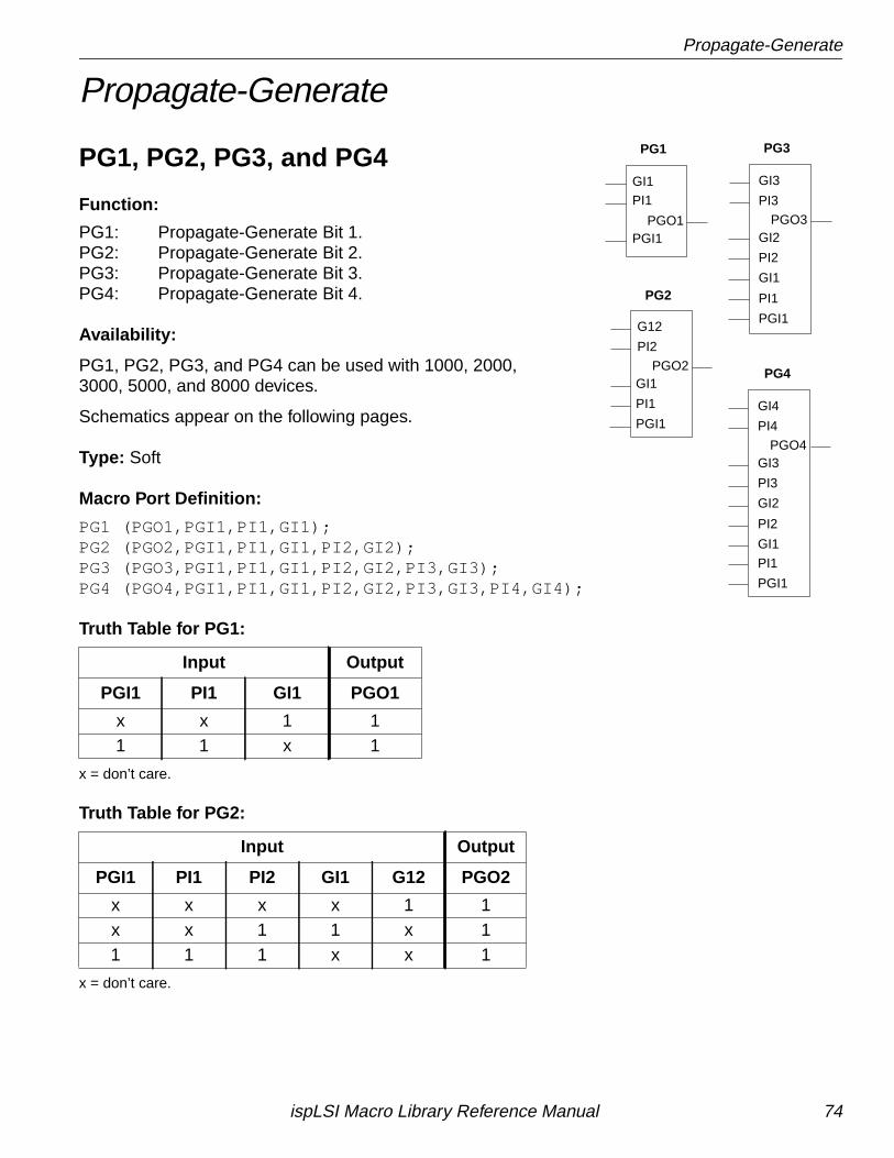
Propagate-Generate
Propagate-Generate
PG1, PG2, PG3, and PG4
Function:
PG1: Propagate-Generate Bit 1.PG2: Propagate-Generate Bit 2.PG3: Propagate-Generate Bit 3.PG4: Propagate-Generate Bit 4.
Availability:
PG1, PG2, PG3, and PG4 can be used with 1000, 2000,3000, 5000, and 8000 devices.
Schematics appear on the following pages.
Type: Soft
Macro Port Definition:
PG1 (PGO1,PGI1,PI1,GI1);PG2 (PGO2,PGI1,PI1,GI1,PI2,GI2);PG3 (PGO3,PGI1,PI1,GI1,PI2,GI2,PI3,GI3);PG4 (PGO4,PGI1,PI1,GI1,PI2,GI2,PI3,GI3,PI4,GI4);
Truth Table for PG1:
x = don’t care.
Truth Table for PG2:
x = don’t care.
Input Output
PGI1 PI1 GI1 PGO1
x x 1 11 1 x 1
Input Output
PGI1 PI1 PI2 GI1 G12 PGO2
x x x x 1 1x x 1 1 x 11 1 1 x x 1
PG1
PGO1
PI1
PGI1
GI1
PG2
PGO2
PI2
GI1
G12
PI1
PGI1
PG3
PGO3
PI3
GI2
GI3
PI2
GI1
PI1
PGI1
PG4
PGO4
PI4
GI3
GI4
PI3
GI2
PI2
GI1
PI1
PGI1
ispLSI Macro Library Reference Manual 74
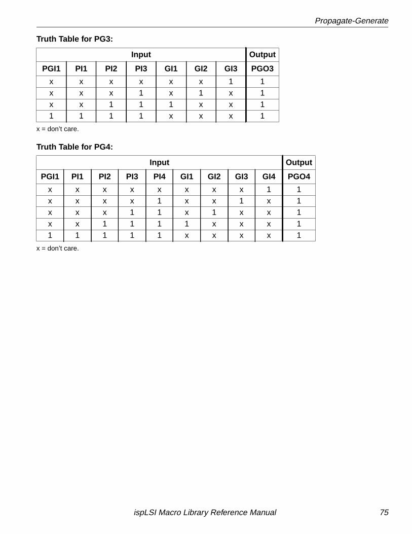
Propagate-Generate
Truth Table for PG3:
x = don’t care.
Truth Table for PG4:
x = don’t care.
Input Output
PGI1 PI1 PI2 PI3 GI1 GI2 GI3 PGO3
x x x x x x 1 1x x x 1 x 1 x 1x x 1 1 1 x x 11 1 1 1 x x x 1
Input Output
PGI1 PI1 PI2 PI3 PI4 GI1 GI2 GI3 GI4 PGO4
x x x x x x x x 1 1x x x x 1 x x 1 x 1x x x 1 1 x 1 x x 1x x 1 1 1 1 x x x 11 1 1 1 1 x x x x 1
ispLSI Macro Library Reference Manual 75
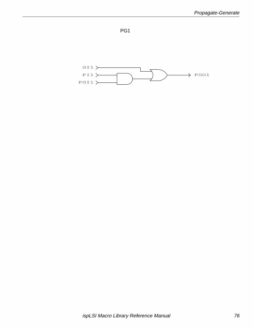
Propagate-Generate
PGO1PI1
PGI1
GI1
PG1
ispLSI Macro Library Reference Manual 76
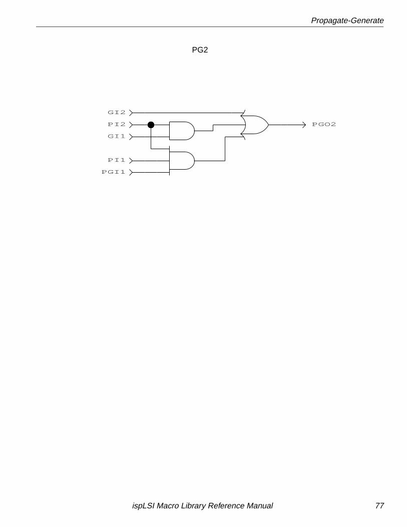
Propagate-Generate
PGO2
GI2
PI2
GI1
PI1
PGI1
PG2
ispLSI Macro Library Reference Manual 77
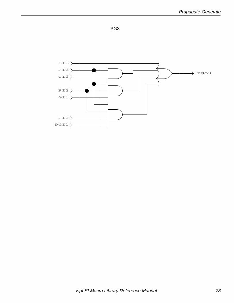
Propagate-Generate
PGO3
PGI1
PI1
GI1
PI2
GI2
PI3
GI3
PG3
ispLSI Macro Library Reference Manual 78
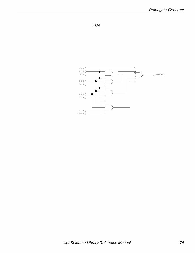
Propagate-Generate
PGO4
GI4
PI4
GI3
PI3
GI2
PI2
GI1
PI1
PGI1
PG4
ispLSI Macro Library Reference Manual 79
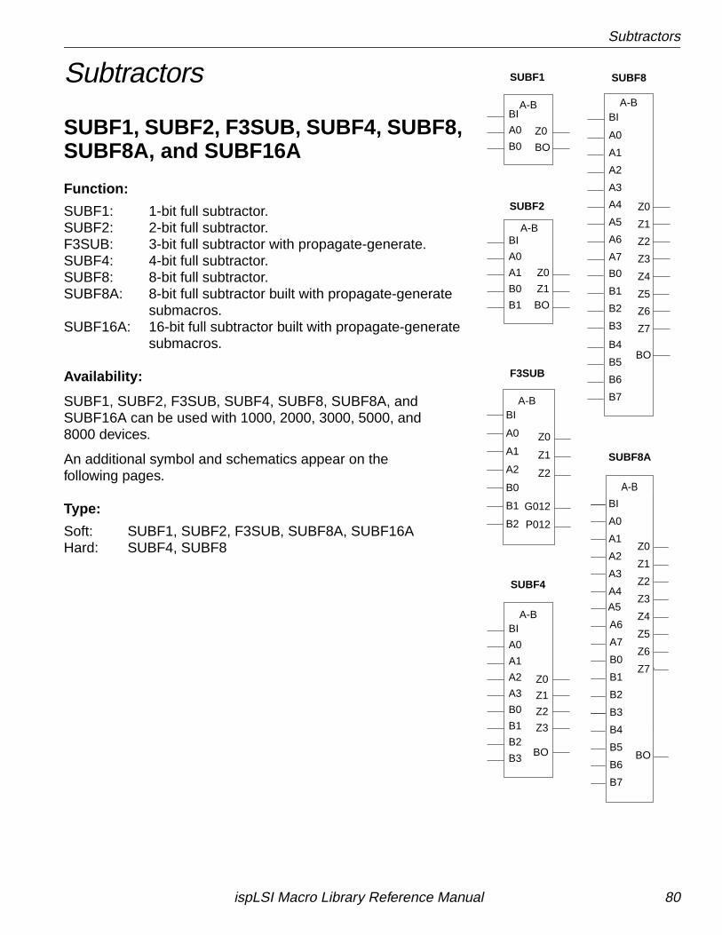
Subtractors
Subtractors
SUBF1, SUBF2, F3SUB, SUBF4, SUBF8,SUBF8A, and SUBF16A
Function:
SUBF1: 1-bit full subtractor.SUBF2: 2-bit full subtractor.F3SUB: 3-bit full subtractor with propagate-generate.SUBF4: 4-bit full subtractor.SUBF8: 8-bit full subtractor.SUBF8A: 8-bit full subtractor built with propagate-generate
submacros.SUBF16A: 16-bit full subtractor built with propagate-generate
submacros.
Availability:
SUBF1, SUBF2, F3SUB, SUBF4, SUBF8, SUBF8A, andSUBF16A can be used with 1000, 2000, 3000, 5000, and8000 devices.
An additional symbol and schematics appear on thefollowing pages.
Type:
Soft: SUBF1, SUBF2, F3SUB, SUBF8A, SUBF16AHard: SUBF4, SUBF8
SUBF1
SUBF2
SUBF4
Z0
BO
A0
B0
BI
BO
Z1
Z0A1
BI
B1
B0
A0
Z1
Z0
Z2
Z3
BO
BI
A2
A3
B0
B1
B2
B3
A1
A0
A-B
A-B
A-B
F3SUB
BI
A0
A1
A2
B0
B1
B2
Z0
Z1
Z2
G012
P012
A-B
Z5
Z4
Z6
Z7
BO
Z1
Z0
Z2
Z3
SUBF8
A4
A5
A6
A7
B0
B1
B2
B3
B4
B5
B6
B7
A0
A1
A2
A3
BIA-B
A-B
SUBF8A
C1A0A1A2A3A4A5
B4
A6A7B0B1B2B3
Z0Z1Z2Z3Z4Z5Z6
B7
B5B6
Z7
C1
BI
A0
A1
A2
A3
A4
A5
B4
A6
A7
B0
B1
B2
B3
Z0
Z1
Z2
Z3
Z4
Z5
Z6
B7
B5
B6
Z7
BO
A-B
ispLSI Macro Library Reference Manual 80
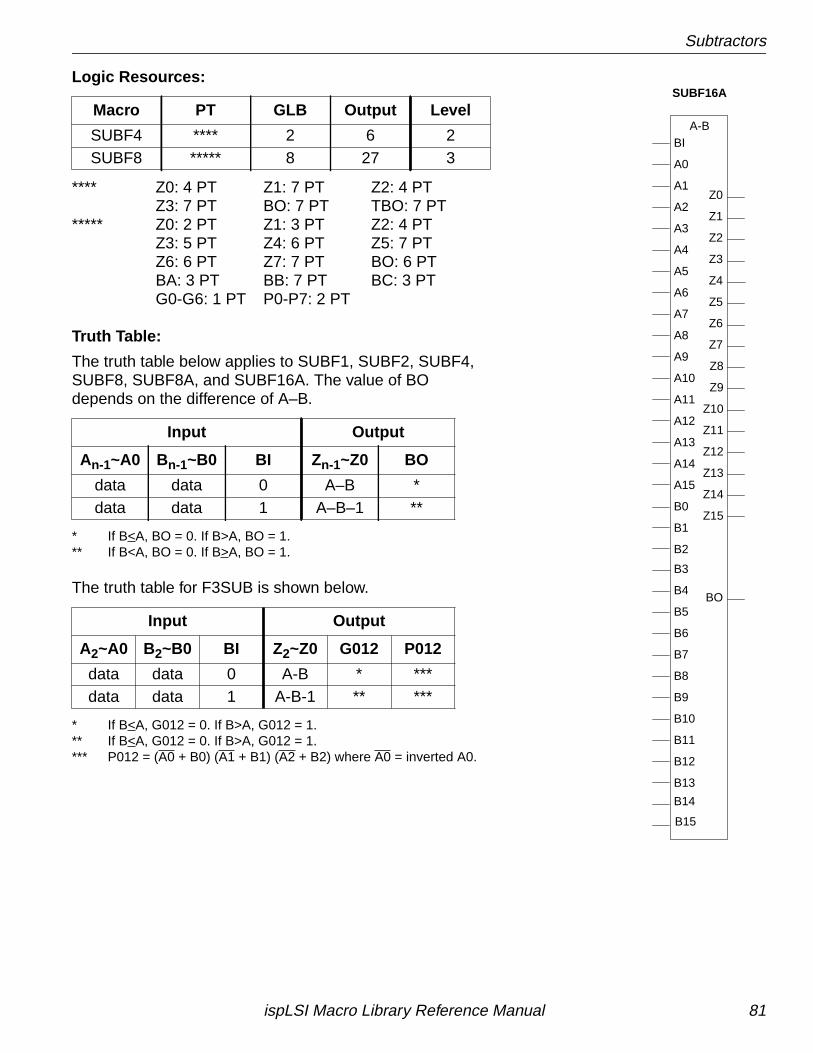
Subtractors
Logic Resources:
**** Z0: 4 PT Z1: 7 PT Z2: 4 PTZ3: 7 PT BO: 7 PT TBO: 7 PT
***** Z0: 2 PT Z1: 3 PT Z2: 4 PTZ3: 5 PT Z4: 6 PT Z5: 7 PTZ6: 6 PT Z7: 7 PT BO: 6 PTBA: 3 PT BB: 7 PT BC: 3 PTG0-G6: 1 PT P0-P7: 2 PT
Truth Table:
The truth table below applies to SUBF1, SUBF2, SUBF4,SUBF8, SUBF8A, and SUBF16A. The value of BOdepends on the difference of A–B.
* If B<A, BO = 0. If B>A, BO = 1.** If B<A, BO = 0. If B>A, BO = 1.
The truth table for F3SUB is shown below.
* If B<A, G012 = 0. If B>A, G012 = 1.** If B<A, G012 = 0. If B>A, G012 = 1.*** P012 = (A0 + B0) (A1 + B1) (A2 + B2) where A0 = inverted A0.
Macro PT GLB Output Level
SUBF4 **** 2 6 2SUBF8 ***** 8 27 3
Input Output
An-1~A0 Bn-1~B0 BI Zn-1~Z0 BO
data data 0 A–B *data data 1 A–B–1 **
Input Output
A2~A0 B2~B0 BI Z2~Z0 G012 P012
data data 0 A-B * ***data data 1 A-B-1 ** ***
BI
A0
A1
A2
A3
A4
A5
A12
A6
A7
A8
A9
A10
A11
Z0
Z1
Z2
Z3
Z4
Z5
Z6
A15
A13
A14
Z7
BO
B0
B1
B2
B3
B4
B5
B6
B11
B7
B8
B9
B10
B14
B12
B13
B15
Z8
Z9
Z10
Z11
Z12
Z13
Z14
Z15
SUBF16A
A-B
ispLSI Macro Library Reference Manual 81
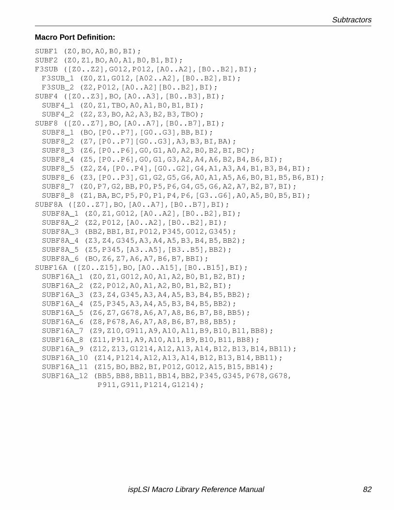
Subtractors
Macro Port Definition:
SUBF1 (Z0,BO,A0,B0,BI);SUBF2 (Z0,Z1,BO,A0,A1,B0,B1,BI);F3SUB ([Z0..Z2],G012,P012,[A0..A2],[B0..B2],BI);
F3SUB_1 (Z0,Z1,G012,[A02..A2],[B0..B2],BI);F3SUB_2 (Z2,P012,[A0..A2][B0..B2],BI);
SUBF4 ([Z0..Z3],BO,[A0..A3],[B0..B3],BI);SUBF4_1 (Z0,Z1,TBO,A0,A1,B0,B1,BI);SUBF4_2 (Z2,Z3,BO,A2,A3,B2,B3,TBO);
SUBF8 ([Z0..Z7],BO,[A0..A7],[B0..B7],BI);SUBF8_1 (BO,[P0..P7],[G0..G3],BB,BI);SUBF8_2 (Z7,[P0..P7][G0..G3],A3,B3,BI,BA);SUBF8_3 (Z6,[P0..P6],G0,G1,A0,A2,B0,B2,BI,BC);SUBF8_4 (Z5,[P0..P6],G0,G1,G3,A2,A4,A6,B2,B4,B6,BI);SUBF8_5 (Z2,Z4,[P0..P4],[G0..G2],G4,A1,A3,A4,B1,B3,B4,BI);SUBF8_6 (Z3,[P0..P3],G1,G2,G5,G6,A0,A1,A5,A6,B0,B1,B5,B6,BI);SUBF8_7 (Z0,P7,G2,BB,P0,P5,P6,G4,G5,G6,A2,A7,B2,B7,BI);SUBF8_8 (Z1,BA,BC,P5,P0,P1,P4,P6,[G3..G6],A0,A5,B0,B5,BI);
SUBF8A ([Z0..Z7],BO,[A0..A7],[B0..B7],BI);SUBF8A_1 (Z0,Z1,G012,[A0..A2],[B0..B2],BI);SUBF8A_2 (Z2,P012,[A0..A2],[B0..B2],BI);SUBF8A_3 (BB2,BBI,BI,P012,P345,G012,G345);SUBF8A_4 (Z3,Z4,G345,A3,A4,A5,B3,B4,B5,BB2);SUBF8A_5 (Z5,P345,[A3..A5],[B3..B5],BB2);SUBF8A_6 (BO,Z6,Z7,A6,A7,B6,B7,BBI);
SUBF16A ([Z0..Z15],BO,[A0..A15],[B0..B15],BI);SUBF16A_1 (Z0,Z1,G012,A0,A1,A2,B0,B1,B2,BI);SUBF16A_2 (Z2,P012,A0,A1,A2,B0,B1,B2,BI);SUBF16A_3 (Z3,Z4,G345,A3,A4,A5,B3,B4,B5,BB2);SUBF16A_4 (Z5,P345,A3,A4,A5,B3,B4,B5,BB2);SUBF16A_5 (Z6,Z7,G678,A6,A7,A8,B6,B7,B8,BB5);SUBF16A_6 (Z8,P678,A6,A7,A8,B6,B7,B8,BB5);SUBF16A_7 (Z9,Z10,G911,A9,A10,A11,B9,B10,B11,BB8);SUBF16A_8 (Z11,P911,A9,A10,A11,B9,B10,B11,BB8);SUBF16A_9 (Z12,Z13,G1214,A12,A13,A14,B12,B13,B14,BB11);SUBF16A_10 (Z14,P1214,A12,A13,A14,B12,B13,B14,BB11);SUBF16A_11 (Z15,BO,BB2,BI,P012,G012,A15,B15,BB14);SUBF16A_12 (BB5,BB8,BB11,BB14,BB2,P345,G345,P678,G678,
P911,G911,P1214,G1214);
ispLSI Macro Library Reference Manual 82
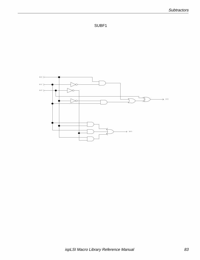
Subtractors
BI
B0
A0
Z0
BO
SUBF1
ispLSI Macro Library Reference Manual 83
Subtractors
BI
LX2
BO
Z0
Z1
B0
B1
A0
A1 A1
A0A0
A1
A[0:1]
A1
A0
A0
A0
B0
B1
B[0:1]
B0B0
B1
B0
B1
B1
BI
BI
A0
A1
A1
A0
A0
A1
A0
A0
A0
A1
A0
A1
A[0:1]
B0
B0
B1
B0
B1
B1
B1
B0
B[0:1]
B1
B0
B1
B1
B0
B0
B1
B1
B0
B0
SUBF2
ispLSI Macro Library Reference Manual 84
Subtractors
B1
B2
B1
B1
B[0:2]
B1
B2
B0
B2
B0B2
B0
B1
B0
B1
B0
B0
B1
B2
B1
B2
B1
B0
B0
B0
G012
Z1LX2
LX2 Z0
B2
A2
B0
A0
A1
B1
BI
P012
BI
B0
B1
B2
B[0:2]
B1
B0
B0
B1
B0
B1
B0
B1
B2
A0
A1
A2
A0
A2
A1
A1
A0
A0
A[0:2]
A2
A1
A0
A0
A2
A1
A1
A1
A0
A1
A2
A0
A0
A[0:2]
A0
A0
A1
A2
A0
A2
A2
A0
F3SUB.1
ispLSI Macro Library Reference Manual 85
Subtractors
BI
BI
BI
BI
BI
B2
B1
B2
B1
B2
B2
B0
B0
B2
B2
B[0:2]
B1
B0
B2
B1
B0
B2
B2
B0
B0
B1
B2
B1
B[0:2]
B2
B0
B2
B0
B1
B2
B2
B1
BI
BI
BI
BI
A0
A0
A0
A1
A1
A1
A0
A1
A[0:1]
A[0:2]
A0
A2
A0
A1
A0
A1
A1
A0
A1
Z2LX2
F3SUB. 2
ispLSI Macro Library Reference Manual 86
Subtractors
BI
B3
B2
A3
A2
BO
Z3
Z2
Z0
Z1
A0
A1
B0
B1
PRESERVE
A-B
A0
B0
B1
BI
A1 Z0
Z1
BO
SUBF2
A-B
A0
B0
B1
BI
A1 Z0
Z1
BO
SUBF2
SUBF4
ispLSI Macro Library Reference Manual 87
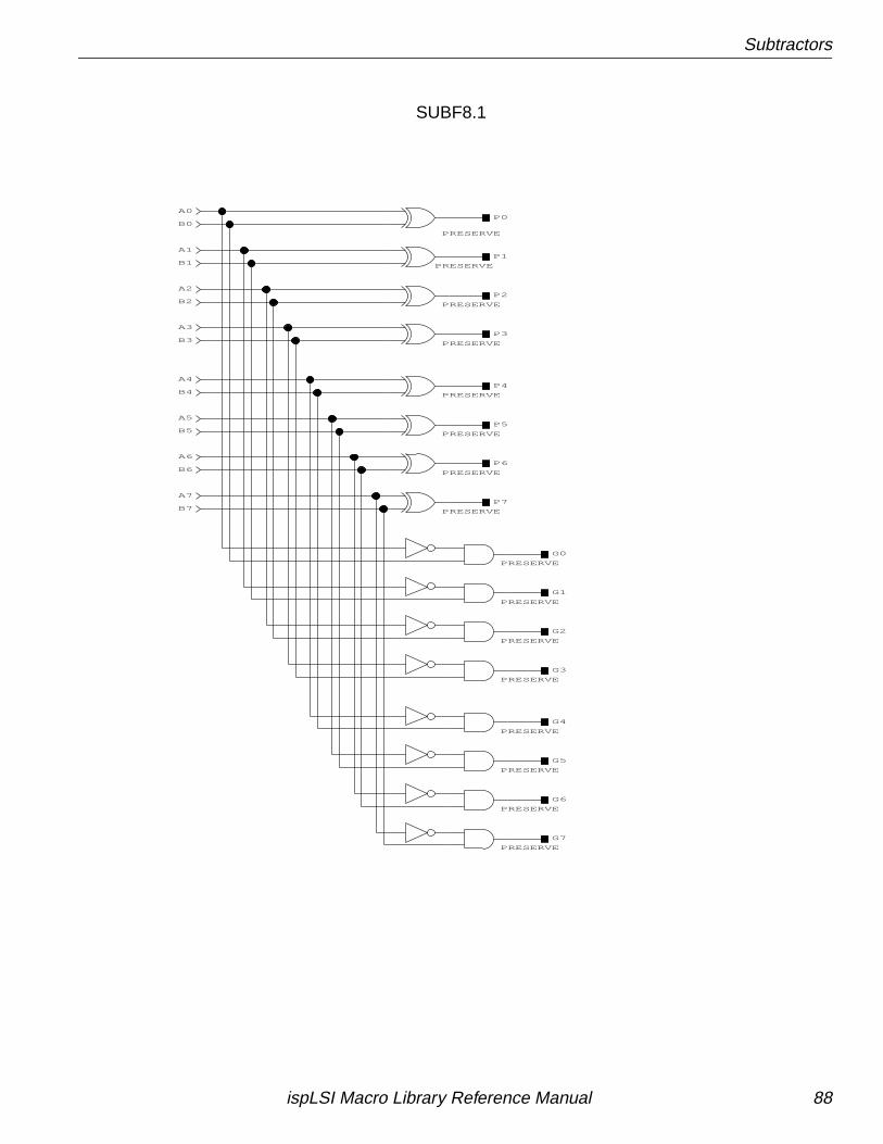
Subtractors
G7
PRESERVE
G6
PRESERVE
G5
PRESERVE
G4
PRESERVE
G3
PRESERVE
G2
PRESERVE
G1
PRESERVE
G0
PRESERVE
P7
PRESERVE
P6
PRESERVE
P5
PRESERVE
P4
PRESERVE
P3
PRESERVE
P2
PRESERVE
P1
PRESERVE
P0
PRESERVE
B0
A0
A3
B3
A2
B2
A1
B1
B4
A4
B5
A5
B6
A6
B7
A7
SUBF8.1
ispLSI Macro Library Reference Manual 88
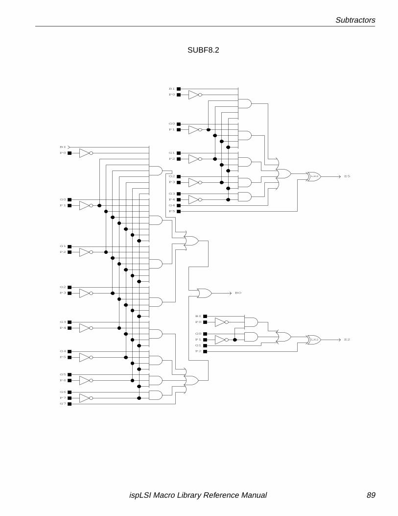
Subtractors
BO
P2
G1
P1
G0
P0
BI
G4
P5
Z5LX2
P4
G3
G2
G1
G0
BI
P3
P2
P0
P1
P7
P6
P5
G6
G5
G4
P4
G2
G3
P3
G1
P2
P1
P0
G0
BI
Z2LX2
G7
SUBF8.2
ispLSI Macro Library Reference Manual 89
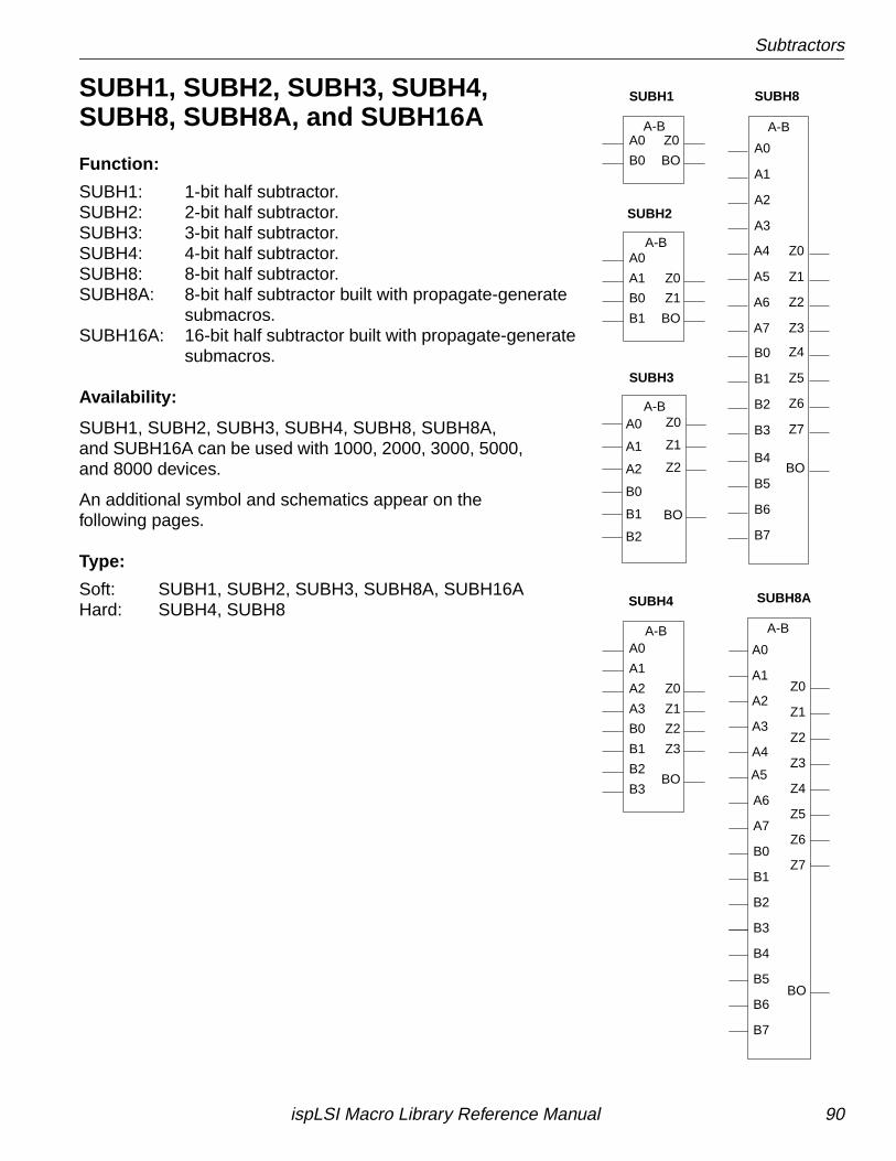
Subtractors
SUBH1, SUBH2, SUBH3, SUBH4,SUBH8, SUBH8A, and SUBH16A
Function:
SUBH1: 1-bit half subtractor.SUBH2: 2-bit half subtractor.SUBH3: 3-bit half subtractor.SUBH4: 4-bit half subtractor.SUBH8: 8-bit half subtractor.SUBH8A: 8-bit half subtractor built with propagate-generate
submacros.SUBH16A: 16-bit half subtractor built with propagate-generate
submacros.
Availability:
SUBH1, SUBH2, SUBH3, SUBH4, SUBH8, SUBH8A,and SUBH16A can be used with 1000, 2000, 3000, 5000,and 8000 devices.
An additional symbol and schematics appear on thefollowing pages.
Type:
Soft: SUBH1, SUBH2, SUBH3, SUBH8A, SUBH16AHard: SUBH4, SUBH8
SUBH1
SUBH2
B0
A0 Z0
BO
BO
Z1
Z0A1
B1
B0
A0
SUBH4
Z1
Z0
Z2
Z3
BO
A2
A3
B0
B1
B2
B3
A1
A0
A-B
A-B
A-B
SUBH3
A0
A1
A2
B0
B1
B2
Z0
Z1
Z2
BO
A-B
SUBH8
Z5
Z4
Z6
Z7
BO
Z1
Z0
Z2
Z3
A4
A5
A6
A7
B0
B1
B2
B3
B4
B5
B6
B7
A0
A1
A2
A3
A-B
SUBH8A
C1A0A1A2A3A4A5
B4
A6A7B0B1B2B3
Z0Z1Z2Z3Z4Z5Z6
B7
B5B6
Z7
C1
A0
A1
A2
A3
A4
A5
B4
A6
A7
B0
B1
B2
B3
Z0
Z1
Z2
Z3
Z4
Z5
Z6
B7
B5
B6
Z7
BO
A-B
ispLSI Macro Library Reference Manual 90
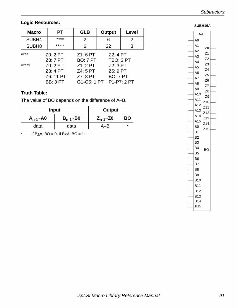
Subtractors
Logic Resources:
**** Z0: 2 PT Z1: 6 PT Z2: 4 PTZ3: 7 PT BO: 7 PT TBO: 3 PT
***** Z0: 2 PT Z1: 2 PT Z2: 3 PTZ3: 4 PT Z4: 5 PT Z5: 9 PTZ6: 11 PT Z7: 8 PT BO: 7 PTBB: 3 PT G1-G5: 1 PT P1-P7: 2 PT
Truth Table:
The value of BO depends on the difference of A–B.
* If B<A, BO = 0. If B>A, BO = 1.
Macro PT GLB Output Level
SUBH4 **** 2 6 2SUBH8 ***** 6 22 3
Input Output
An-1~A0 Bn-1~B0 Zn-1~Z0 BO
data data A–B *
SUBH16A
A0
A1
A2
A3
A4
A5
A12
A6
A7
A8
A9
A10
A11
Z0
Z1
Z2
Z3
Z4
Z5
Z6
A15
A13
A14
Z7
BO
B0
B1
B2B3
B4
B5
B6
B11
B7
B8
B9
B10
B14
B12
B13
B15
Z8
Z9
Z10
Z11
Z12
Z13
Z14
Z15
A-B
ispLSI Macro Library Reference Manual 91
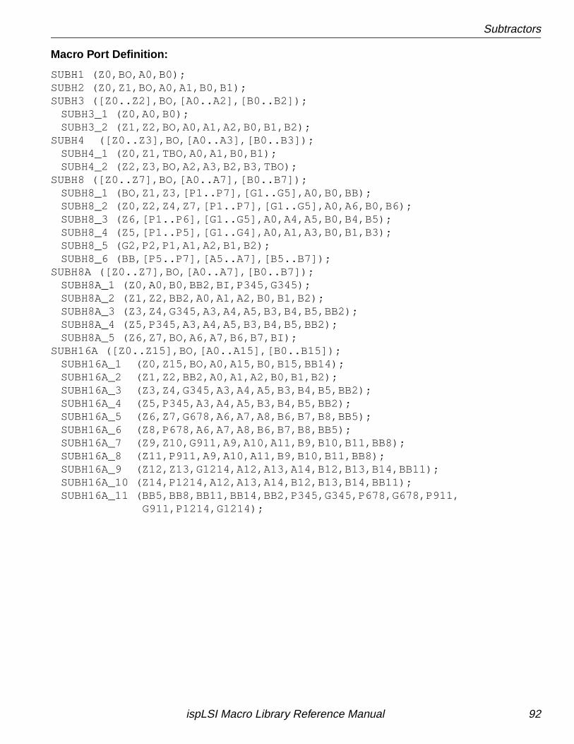
Subtractors
Macro Port Definition:
SUBH1 (Z0,BO,A0,B0);SUBH2 (Z0,Z1,BO,A0,A1,B0,B1);SUBH3 ([Z0..Z2],BO,[A0..A2],[B0..B2]);
SUBH3_1 (Z0,A0,B0);SUBH3_2 (Z1,Z2,BO,A0,A1,A2,B0,B1,B2);
SUBH4 ([Z0..Z3],BO,[A0..A3],[B0..B3]);SUBH4_1 (Z0,Z1,TBO,A0,A1,B0,B1);SUBH4_2 (Z2,Z3,BO,A2,A3,B2,B3,TBO);
SUBH8 ([Z0..Z7],BO,[A0..A7],[B0..B7]);SUBH8_1 (BO,Z1,Z3,[P1..P7],[G1..G5],A0,B0,BB);SUBH8_2 (Z0,Z2,Z4,Z7,[P1..P7],[G1..G5],A0,A6,B0,B6);SUBH8_3 (Z6,[P1..P6],[G1..G5],A0,A4,A5,B0,B4,B5);SUBH8_4 (Z5,[P1..P5],[G1..G4],A0,A1,A3,B0,B1,B3);SUBH8_5 (G2,P2,P1,A1,A2,B1,B2);SUBH8_6 (BB,[P5..P7],[A5..A7],[B5..B7]);
SUBH8A ([Z0..Z7],BO,[A0..A7],[B0..B7]);SUBH8A_1 (Z0,A0,B0,BB2,BI,P345,G345);SUBH8A_2 (Z1,Z2,BB2,A0,A1,A2,B0,B1,B2);SUBH8A_3 (Z3,Z4,G345,A3,A4,A5,B3,B4,B5,BB2);SUBH8A_4 (Z5,P345,A3,A4,A5,B3,B4,B5,BB2);SUBH8A_5 (Z6,Z7,BO,A6,A7,B6,B7,BI);
SUBH16A ([Z0..Z15],BO,[A0..A15],[B0..B15]);SUBH16A_1 (Z0,Z15,BO,A0,A15,B0,B15,BB14);SUBH16A_2 (Z1,Z2,BB2,A0,A1,A2,B0,B1,B2);SUBH16A_3 (Z3,Z4,G345,A3,A4,A5,B3,B4,B5,BB2);SUBH16A_4 (Z5,P345,A3,A4,A5,B3,B4,B5,BB2);SUBH16A_5 (Z6,Z7,G678,A6,A7,A8,B6,B7,B8,BB5);SUBH16A_6 (Z8,P678,A6,A7,A8,B6,B7,B8,BB5);SUBH16A_7 (Z9,Z10,G911,A9,A10,A11,B9,B10,B11,BB8);SUBH16A_8 (Z11,P911,A9,A10,A11,B9,B10,B11,BB8);SUBH16A_9 (Z12,Z13,G1214,A12,A13,A14,B12,B13,B14,BB11);SUBH16A_10 (Z14,P1214,A12,A13,A14,B12,B13,B14,BB11);SUBH16A_11 (BB5,BB8,BB11,BB14,BB2,P345,G345,P678,G678,P911,
G911,P1214,G1214);
ispLSI Macro Library Reference Manual 92
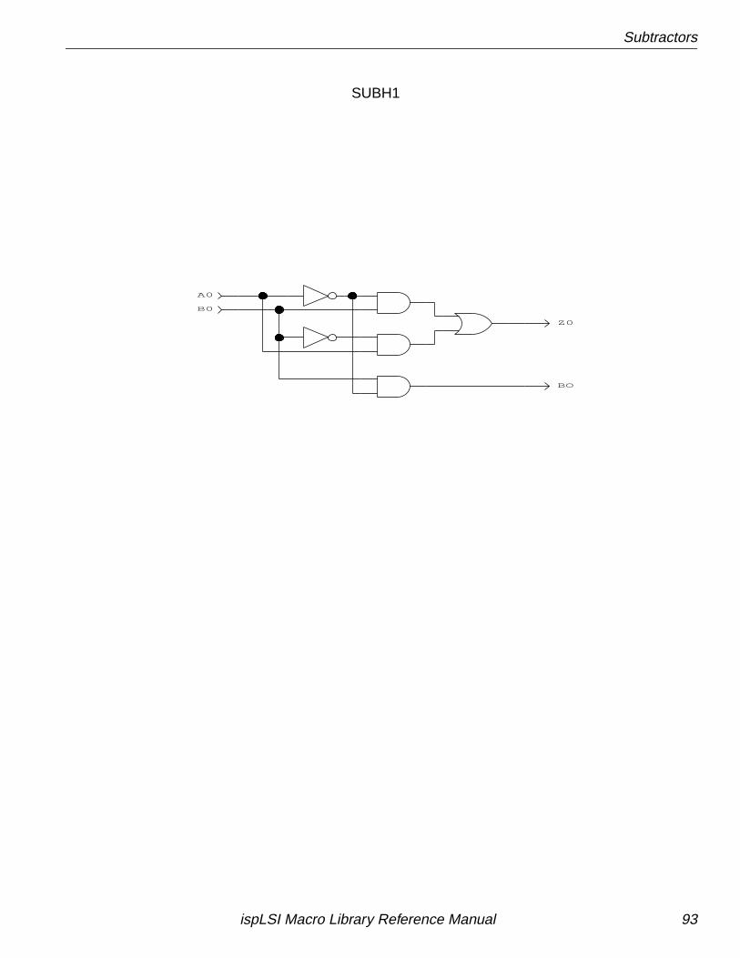
Subtractors
Z0
BO
B0
A0
SUBH1
ispLSI Macro Library Reference Manual 93
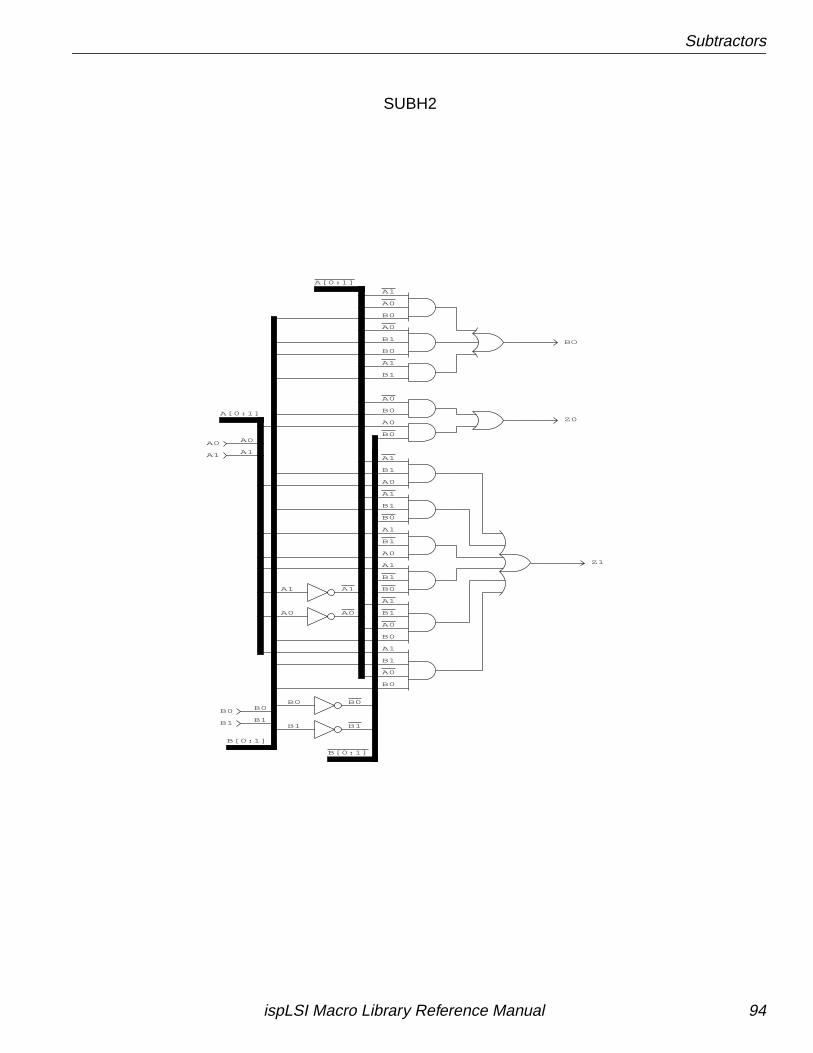
Subtractors
A[0:1]
A0
A0
A1
A0
A0
A1
A1
A1
A0
A1
A1
A1
A1
A0
A1
A0
A0
A1
A0
A0
A0
A1
A[0:1]
B0
B[0:1]
B1
B0
B1
B0
B1
B0
B1
B0
B1
B1
B0B0
B1
B0
B1
Z1
Z0
BO
B[0:1]
B0
B1
B0
B0
B1
B1
B1
B0
A0
A1
SUBH2
ispLSI Macro Library Reference Manual 94
Subtractors
A2
A[0:2]
A2
A0
A0
A1
A2
A1
A2
A1
A0
A2
A0
A1
A1
A2
A1
A0
A[0:2]
A0
A1
A0
A1
A2
A0
B1
B[0:2]
B0
B1
B2
B0
B1
B0
B1
B2
B0
B0
B1B1
B0
B2
B2
B2
B2
B1
B0
B[0:2]
B2
B0
B0
B1
B1
B0
B1
A2
A1
A0
B2
B1
B0
Z1LX2
Z0
BO
A0 A0
SUBH3.1
ispLSI Macro Library Reference Manual 95

Subtractors
Z2LX2
A0
A1
A0
A2
A1
A1
A[0:2]
B2
B2
B2
B1
B0
B1
B0
B2
B[0:2]
B2
B1
B0
B2
B1
B2
B1
B2
B[0:2]
B0
A0
A[0:1]
A1
A1
A0
SUBH3.2
ispLSI Macro Library Reference Manual 96
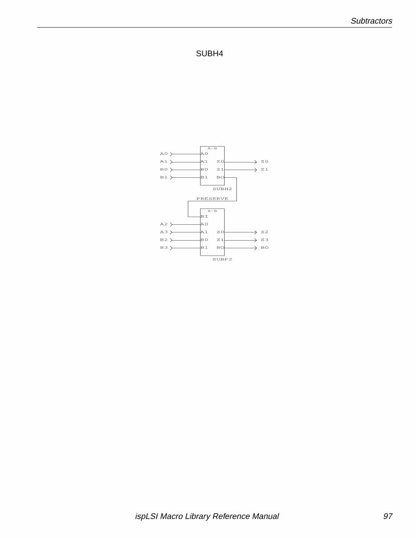
Subtractors
PRESERVE
A-B
A0
B0
B1
BI
A1 Z0
Z1
BO
SUBF2
A-B
A0
B0
B1
A1 Z0
Z1
BO
SUBH2
B1
B0
A1
A0
Z1
Z0
Z2
Z3
BO
A2
A3
B2
B3
SUBH4
ispLSI Macro Library Reference Manual 97
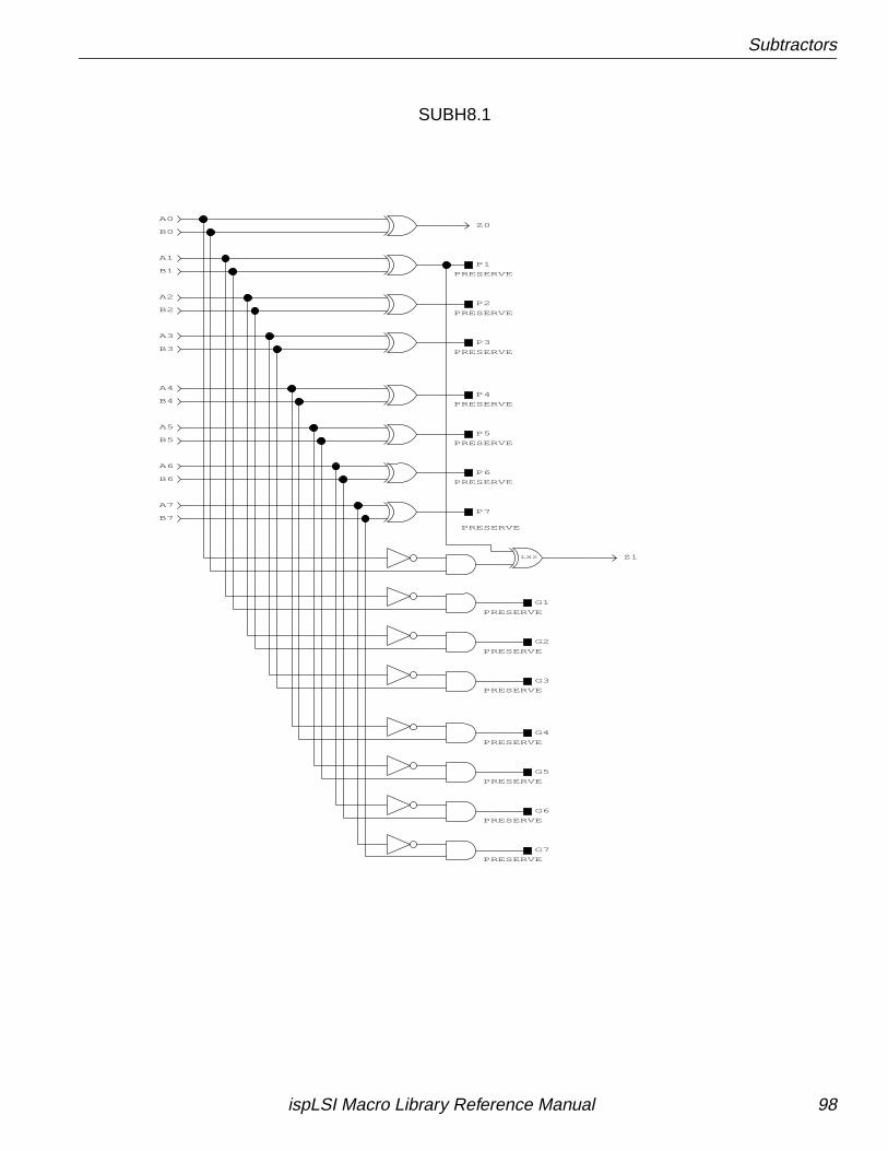
Subtractors
P1
PRESERVE
P2
PRESERVE
P3
PRESERVE
P4
PRESERVE
P5
PRESERVE
P6
PRESERVE
P7
PRESERVE
G1
PRESERVE
G2
PRESERVE
G3
PRESERVE
G4
PRESERVE
G5
PRESERVE
G6
PRESERVE
G7
PRESERVE
LX2
Z0
A7
B7
A6
B6
A5
B5
A4
B4
B1
A1
B2
A2
B3
A3
A0
B0
Z1
SUBH8.1
ispLSI Macro Library Reference Manual 98
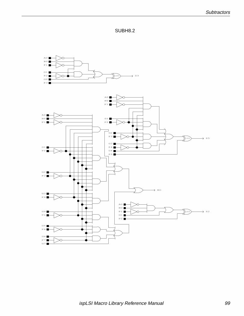
Subtractors
P5
G4
G3
G2
BO
P3
G2
G1
B0
P2
P1
A0
Z5
B0
G1
P4
P3
P2
P1
A0
G7
P2
G1
B0
P1
A0
P5
P7
P6
P4
G6
G5
G4
G3
G2
P3
B0
G1
P2
P1
A0
Z2
Z3LX2
LX2
LX2
SUBH8.2
ispLSI Macro Library Reference Manual 99
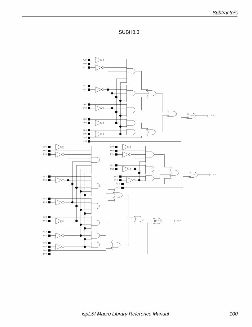
Subtractors
P4
G3
G2
P7
Z7LX2
B0
G1
A0
P1
P2
P3
B0
G1
G2
G3
G4
P6
G5
P5
P4
P3
P2
P1
A0
B0
G1
G2
G3
G4
G5
G6
P6
P5
P4
P3
P2
P1
A0
Z6
Z4LX2
LX2
SUBH8.3
ispLSI Macro Library Reference Manual 100
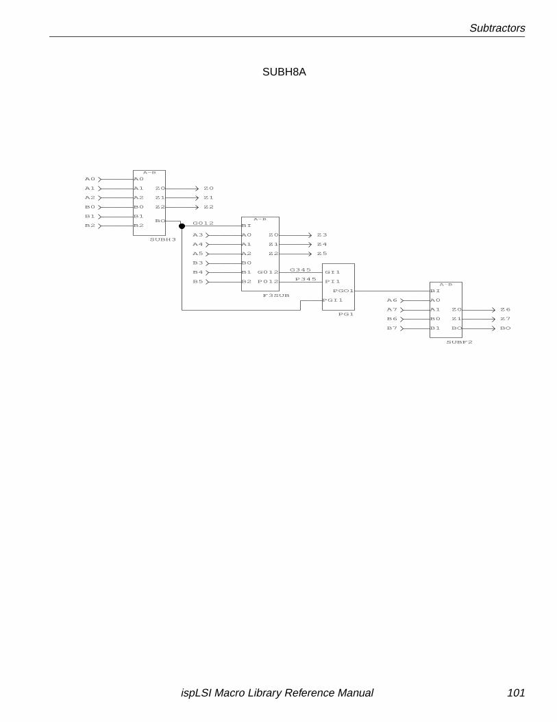
Subtractors
Z4
Z3
B5
B4
B3
A5
A3
A4
Z5
A1
A2
B0
B1
B2
Z1
Z2
Z0
A0
A6
A7
B6
B7
Z6
Z7
BO
P345
G345
G012
A-B
SUBH3
A0
A1
A2
BO
Z2
Z0
Z1
B0
B1
B2
A-B
F3SUB
BI
B2
B1
B0
A2
A1
A0
P012
G012
Z2
Z1
Z0
PGO1
PG1
PGI1
PI1
GI1
A-B
A0
B0
B1
BI
A1 Z0
Z1
BO
SUBF2
SUBH8A
ispLSI Macro Library Reference Manual 101
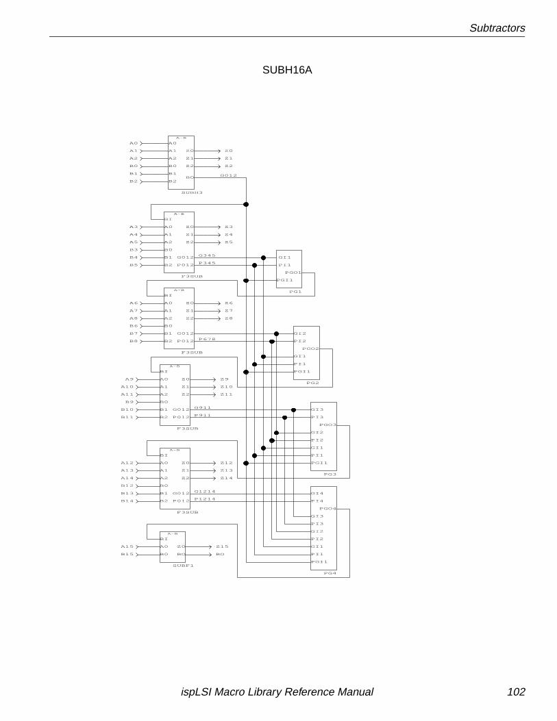
Subtractors
G012
P678
P911
P1214
G1214
Z14
A13
A14
B12
Z13
A0
Z0
Z2
Z1
B2
B1
B0
A2
A1
Z4
Z3
B5
B4
B3
A5
A3
A4
Z5
Z8A8
B6
B7
B8
A7
A6 Z6
Z7
Z12
B14
B13
A12
B11
B10
B9
A11
A10
A9 Z9
Z10
Z11
G911
G345
P345
Z15
BO
A15
B15
A-B
SUBH3
A0
A1
A2
BO
Z2
Z0
Z1
B0
B1
B2
A-B
F3SUB
BI
B2
B1
B0
A2
A1
A0
P012
G012
Z2
Z1
Z0
A-B
F3SUB
BI
B2
B1
B0
A2
A1
A0
P012
G012
Z2
Z1
Z0
A-B
F3SUB
BI
B2
B1
B0
A2
A1
A0
P012
G012
Z2
Z1
Z0
A-B
F3SUB
BI
B2
B1
B0
A2
A1
A0
P012
G012
Z2
Z1
Z0
A-B
SUBF1
Z0
BO
A0
B0
BI
PGO1
PG1
PGI1
PI1
GI1
PGO2
GI1
PI1
PGI1
PG2
GI2
PI2
PGO3
PI3
GI3
PI2
GI2
PI1
PGI1
GI1
PG3
PGO4
PI4
GI4
GI3
PG4
GI1
PGI1
PI1
PI2
PI3
GI2
SUBH16A
ispLSI Macro Library Reference Manual 102
Coders
This chapter contains information on the following macros:
■ Decoders
■ Encoders
ispLSI Macro Library Reference Manual 103
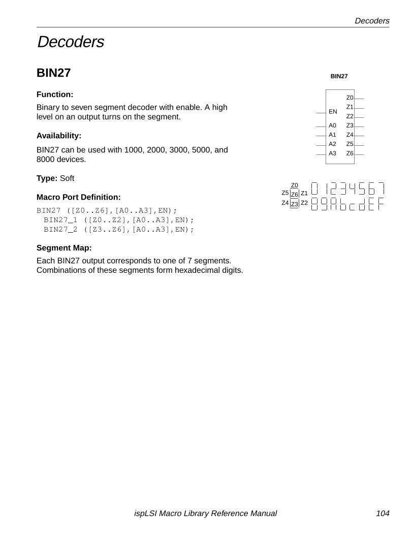
Decoders
Decoders
BIN27
Function:
Binary to seven segment decoder with enable. A highlevel on an output turns on the segment.
Availability:
BIN27 can be used with 1000, 2000, 3000, 5000, and8000 devices.
Type: Soft
Macro Port Definition:
BIN27 ([Z0..Z6],[A0..A3],EN);BIN27_1 ([Z0..Z2],[A0..A3],EN);BIN27_2 ([Z3..Z6],[A0..A3],EN);
Segment Map:
Each BIN27 output corresponds to one of 7 segments.Combinations of these segments form hexadecimal digits.
BIN27
EN
A0
A1
A2
A3 Z6
Z5
Z4
Z3
Z2
Z1
Z0
Z0Z1
Z2Z6
Z3
Z5
Z4
ispLSI Macro Library Reference Manual 104
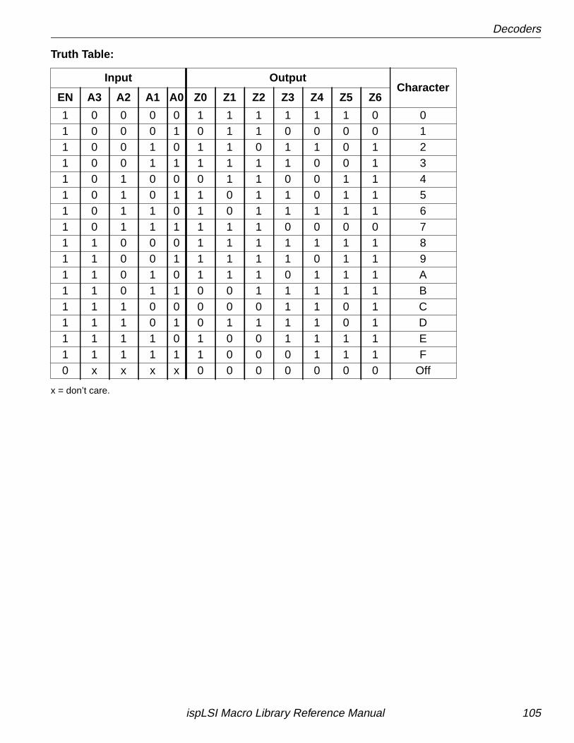
Decoders
Truth Table:
x = don’t care.
Input OutputCharacter
EN A3 A2 A1 A0 Z0 Z1 Z2 Z3 Z4 Z5 Z6
1 0 0 0 0 1 1 1 1 1 1 0 01 0 0 0 1 0 1 1 0 0 0 0 11 0 0 1 0 1 1 0 1 1 0 1 21 0 0 1 1 1 1 1 1 0 0 1 31 0 1 0 0 0 1 1 0 0 1 1 41 0 1 0 1 1 0 1 1 0 1 1 51 0 1 1 0 1 0 1 1 1 1 1 61 0 1 1 1 1 1 1 0 0 0 0 71 1 0 0 0 1 1 1 1 1 1 1 81 1 0 0 1 1 1 1 1 0 1 1 91 1 0 1 0 1 1 1 0 1 1 1 A1 1 0 1 1 0 0 1 1 1 1 1 B1 1 1 0 0 0 0 0 1 1 0 1 C1 1 1 0 1 0 1 1 1 1 0 1 D1 1 1 1 0 1 0 0 1 1 1 1 E1 1 1 1 1 1 0 0 0 1 1 1 F0 x x x x 0 0 0 0 0 0 0 Off
ispLSI Macro Library Reference Manual 105
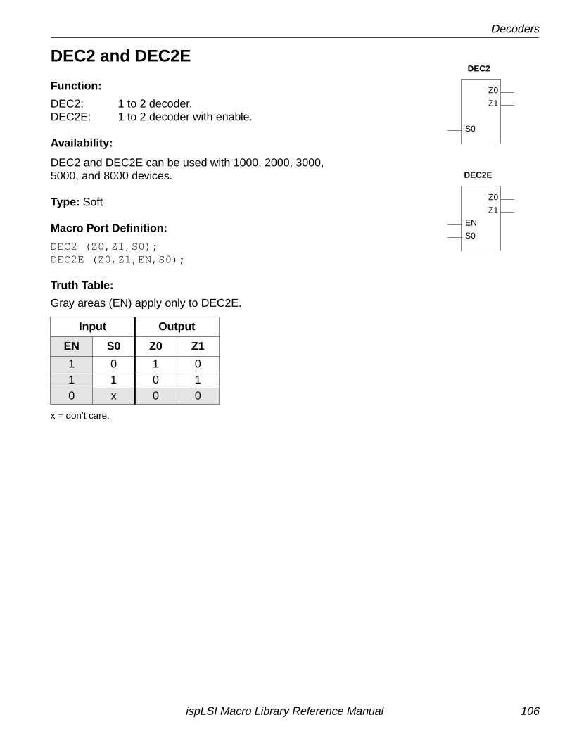
Decoders
DEC2 and DEC2E
Function:
DEC2: 1 to 2 decoder.DEC2E: 1 to 2 decoder with enable.
Availability:
DEC2 and DEC2E can be used with 1000, 2000, 3000,5000, and 8000 devices.
Type: Soft
Macro Port Definition:
DEC2 (Z0,Z1,S0);DEC2E (Z0,Z1,EN,S0);
Truth Table:
Gray areas (EN) apply only to DEC2E.
x = don’t care.
Input Output
EN S0 Z0 Z1
1 0 1 01 1 0 10 x 0 0
Z0
Z1
EN
S0
DEC2
DEC2E
Z1
Z0
S0
ispLSI Macro Library Reference Manual 106
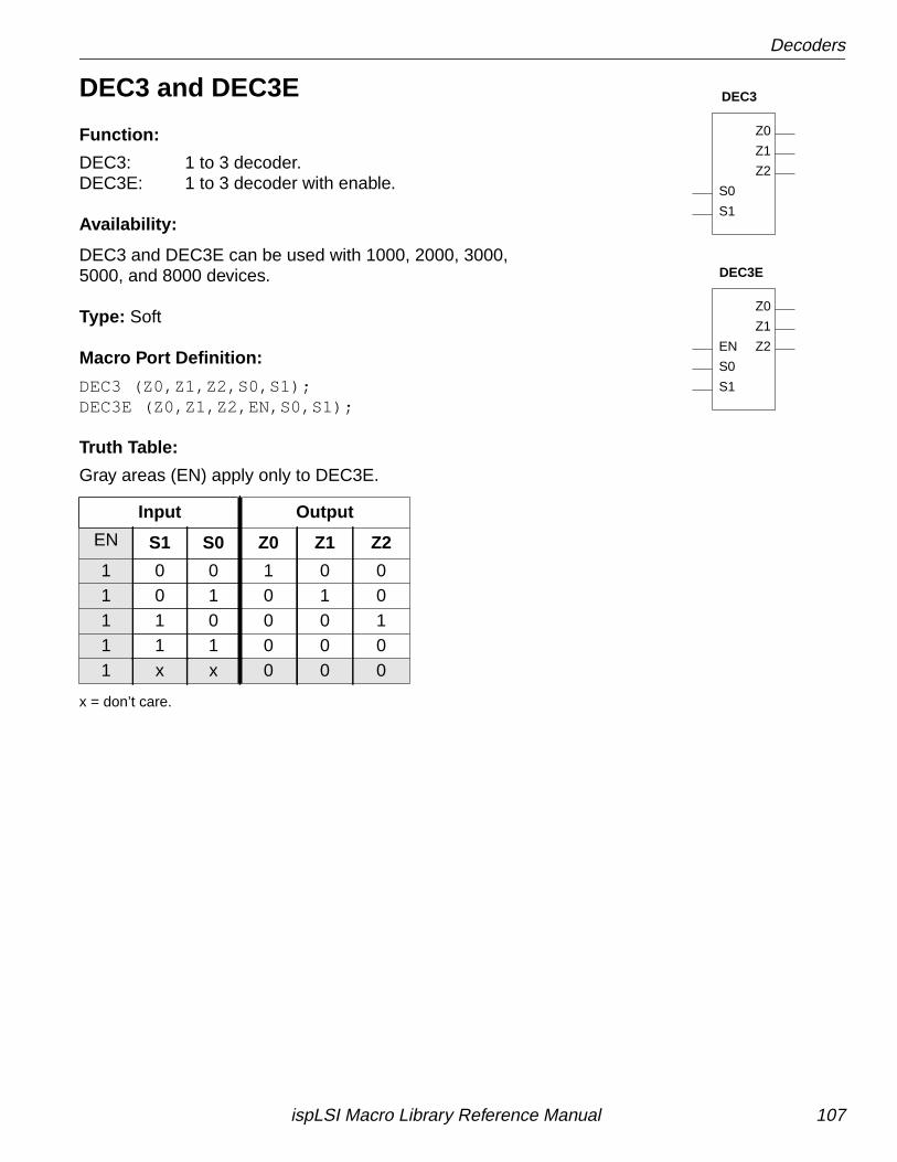
Decoders
DEC3 and DEC3E
Function:
DEC3: 1 to 3 decoder.DEC3E: 1 to 3 decoder with enable.
Availability:
DEC3 and DEC3E can be used with 1000, 2000, 3000,5000, and 8000 devices.
Type: Soft
Macro Port Definition:
DEC3 (Z0,Z1,Z2,S0,S1);DEC3E (Z0,Z1,Z2,EN,S0,S1);
Truth Table:
Gray areas (EN) apply only to DEC3E.
x = don’t care.
Input Output
EN S1 S0 Z0 Z1 Z2
1 0 0 1 0 01 0 1 0 1 01 1 0 0 0 11 1 1 0 0 01 x x 0 0 0
DEC3
DEC3E
Z2
Z1
Z0
EN
S0
S1
Z2
Z1
Z0
S0
S1
ispLSI Macro Library Reference Manual 107
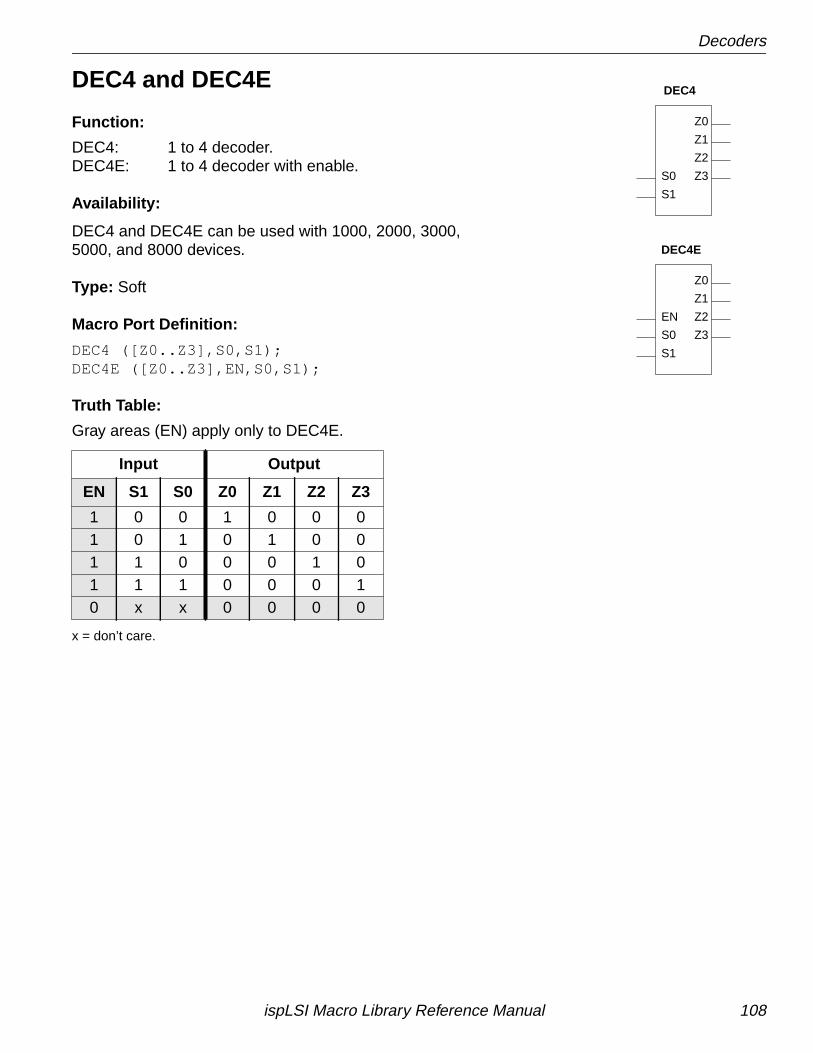
Decoders
DEC4 and DEC4E
Function:
DEC4: 1 to 4 decoder.DEC4E: 1 to 4 decoder with enable.
Availability:
DEC4 and DEC4E can be used with 1000, 2000, 3000,5000, and 8000 devices.
Type: Soft
Macro Port Definition:
DEC4 ([Z0..Z3],S0,S1);DEC4E ([Z0..Z3],EN,S0,S1);
Truth Table:
Gray areas (EN) apply only to DEC4E.
x = don’t care.
Input Output
EN S1 S0 Z0 Z1 Z2 Z3
1 0 0 1 0 0 01 0 1 0 1 0 01 1 0 0 0 1 01 1 1 0 0 0 10 x x 0 0 0 0
Z1
Z0
Z2
Z3S0
S1
Z1
Z0
Z2
Z3
EN
S0
S1
DEC4
DEC4E
ispLSI Macro Library Reference Manual 108
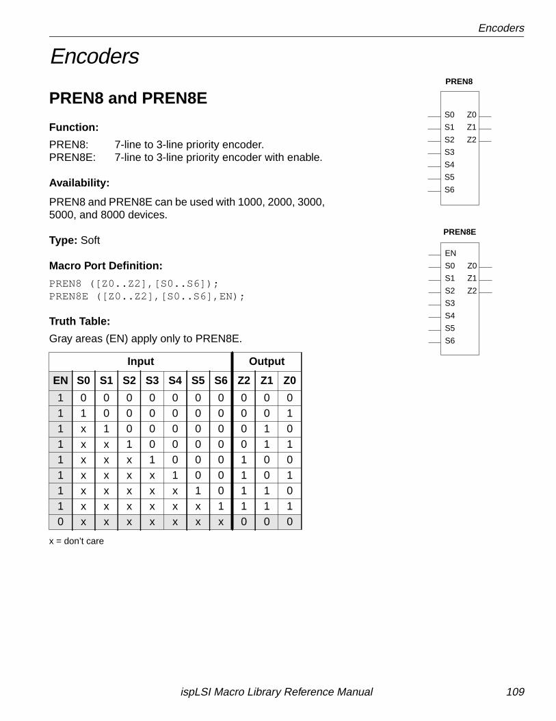
Encoders
Encoders
PREN8 and PREN8E
Function:
PREN8: 7-line to 3-line priority encoder.PREN8E: 7-line to 3-line priority encoder with enable.
Availability:
PREN8 and PREN8E can be used with 1000, 2000, 3000,5000, and 8000 devices.
Type: Soft
Macro Port Definition:
PREN8 ([Z0..Z2],[S0..S6]);PREN8E ([Z0..Z2],[S0..S6],EN);
Truth Table:
Gray areas (EN) apply only to PREN8E.
x = don’t care
Input Output
EN S0 S1 S2 S3 S4 S5 S6 Z2 Z1 Z0
1 0 0 0 0 0 0 0 0 0 01 1 0 0 0 0 0 0 0 0 11 x 1 0 0 0 0 0 0 1 01 x x 1 0 0 0 0 0 1 11 x x x 1 0 0 0 1 0 01 x x x x 1 0 0 1 0 11 x x x x x 1 0 1 1 01 x x x x x x 1 1 1 10 x x x x x x x 0 0 0
PREN8
PREN8E
S0
S1
S2
S3
S4
S5
S6
EN
Z2
Z1
Z0
S0
S1
S2
S3
S4
S5
S6
Z2
Z1
Z0
ispLSI Macro Library Reference Manual 109
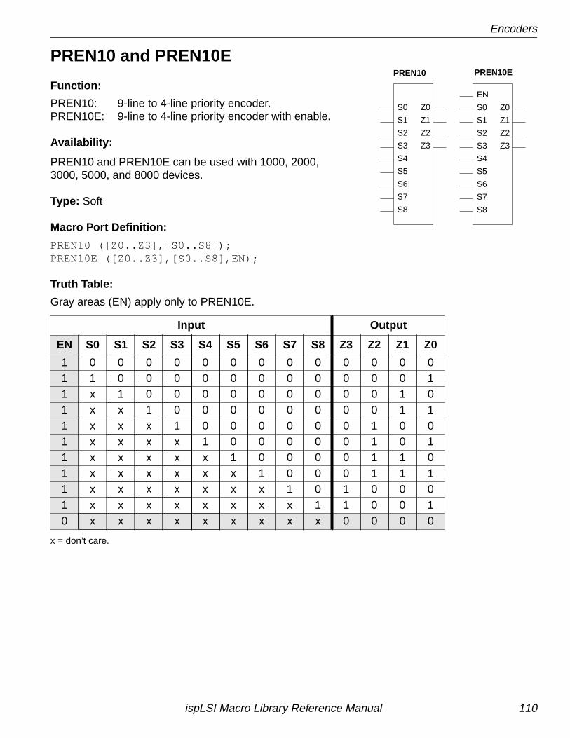
Encoders
PREN10 and PREN10E
Function:
PREN10: 9-line to 4-line priority encoder.PREN10E: 9-line to 4-line priority encoder with enable.
Availability:
PREN10 and PREN10E can be used with 1000, 2000,3000, 5000, and 8000 devices.
Type: Soft
Macro Port Definition:
PREN10 ([Z0..Z3],[S0..S8]);PREN10E ([Z0..Z3],[S0..S8],EN);
Truth Table:
Gray areas (EN) apply only to PREN10E.
x = don’t care.
Input Output
EN S0 S1 S2 S3 S4 S5 S6 S7 S8 Z3 Z2 Z1 Z0
1 0 0 0 0 0 0 0 0 0 0 0 0 01 1 0 0 0 0 0 0 0 0 0 0 0 11 x 1 0 0 0 0 0 0 0 0 0 1 01 x x 1 0 0 0 0 0 0 0 0 1 11 x x x 1 0 0 0 0 0 0 1 0 01 x x x x 1 0 0 0 0 0 1 0 11 x x x x x 1 0 0 0 0 1 1 01 x x x x x x 1 0 0 0 1 1 11 x x x x x x x 1 0 1 0 0 01 x x x x x x x x 1 1 0 0 10 x x x x x x x x x 0 0 0 0
PREN10 PREN10E
S0
S1
S2
S3
S4
S5
S6
S7
S8
EN
Z3
Z2
Z1
Z0S0
S1
S2
S3
S4
S5
S6
S7
S8
Z3
Z2
Z1
Z0
ispLSI Macro Library Reference Manual 110
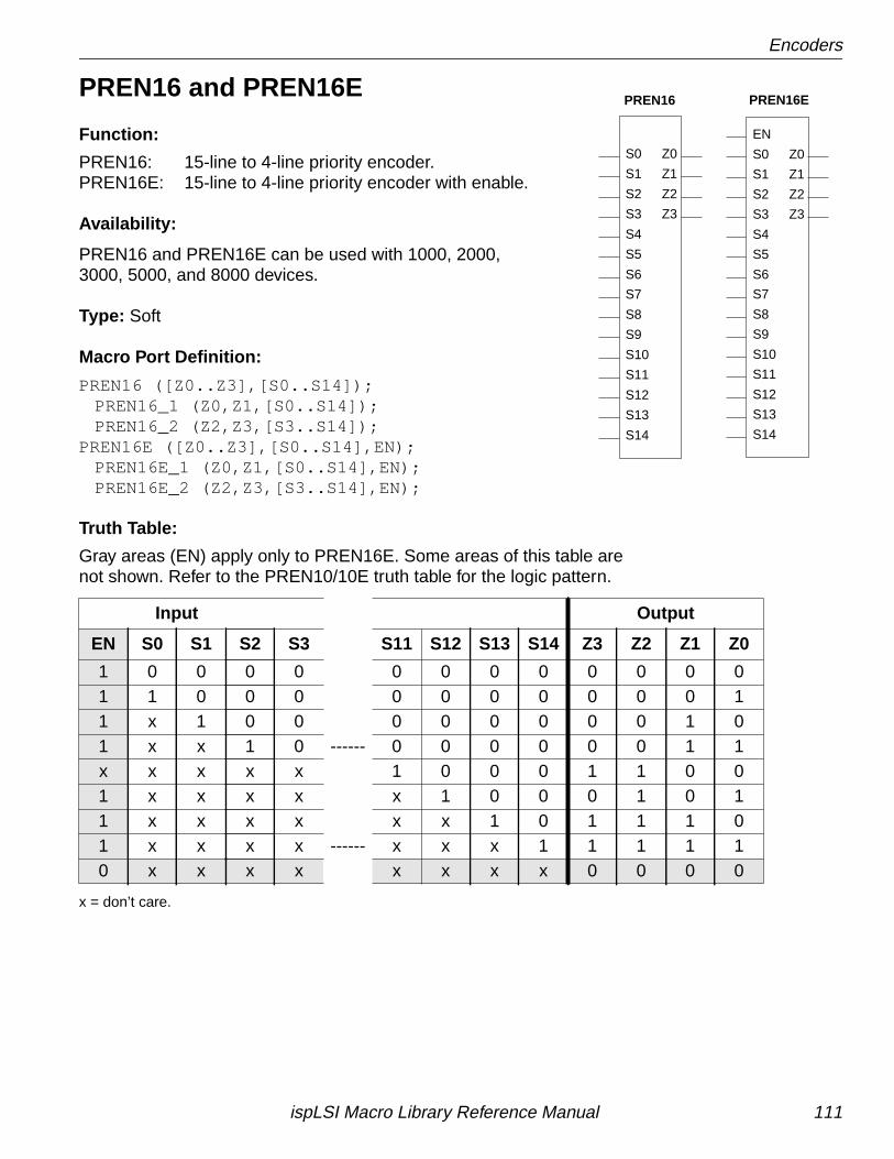
Encoders
PREN16 and PREN16E
Function:
PREN16: 15-line to 4-line priority encoder.PREN16E: 15-line to 4-line priority encoder with enable.
Availability:
PREN16 and PREN16E can be used with 1000, 2000,3000, 5000, and 8000 devices.
Type: Soft
Macro Port Definition:
PREN16 ([Z0..Z3],[S0..S14]);PREN16_1 (Z0,Z1,[S0..S14]);PREN16_2 (Z2,Z3,[S3..S14]);
PREN16E ([Z0..Z3],[S0..S14],EN);PREN16E_1 (Z0,Z1,[S0..S14],EN);PREN16E_2 (Z2,Z3,[S3..S14],EN);
Truth Table:
Gray areas (EN) apply only to PREN16E. Some areas of this table arenot shown. Refer to the PREN10/10E truth table for the logic pattern.
x = don’t care.
Input Output
EN S0 S1 S2 S3 S11 S12 S13 S14 Z3 Z2 Z1 Z0
1 0 0 0 0 0 0 0 0 0 0 0 01 1 0 0 0 0 0 0 0 0 0 0 11 x 1 0 0 0 0 0 0 0 0 1 01 x x 1 0 ------ 0 0 0 0 0 0 1 1x x x x x 1 0 0 0 1 1 0 01 x x x x x 1 0 0 0 1 0 11 x x x x x x 1 0 1 1 1 01 x x x x ------ x x x 1 1 1 1 10 x x x x x x x x 0 0 0 0
PREN16 PREN16E
S0
S1
S2
S3
S4
S5
S6
S7
S13
S12
S11
S10
S9
S14
S8
EN
Z3
Z2
Z1
Z0S0
S1
S2
S3
S4
S5
S6
S7
S13
S12
S11
S10
S9
S14
S8
Z3
Z2
Z1
Z0
ispLSI Macro Library Reference Manual 111
Counters
This chapter contains information on the following macros:
■ Binary Counters
■ Decade Counters
■ Gray Code Counters
ispLSI Macro Library Reference Manual 112
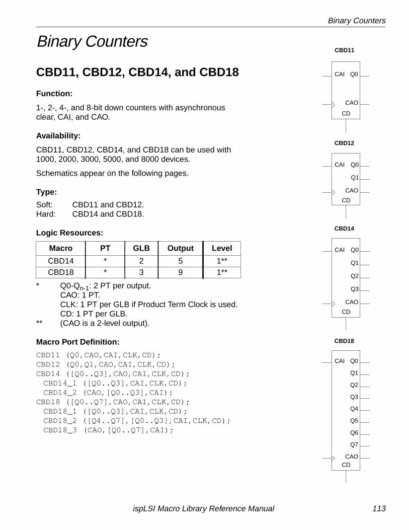
Binary Counters
Binary Counters
CBD11, CBD12, CBD14, and CBD18
Function:
1-, 2-, 4-, and 8-bit down counters with asynchronousclear, CAI, and CAO.
Availability:
CBD11, CBD12, CBD14, and CBD18 can be used with1000, 2000, 3000, 5000, and 8000 devices.
Schematics appear on the following pages.
Type:
Soft: CBD11 and CBD12.Hard: CBD14 and CBD18.
Logic Resources:
* Q0-Qn-1: 2 PT per output.CAO: 1 PT.CLK: 1 PT per GLB if Product Term Clock is used.CD: 1 PT per GLB.
** (CAO is a 2-level output).
Macro Port Definition:
CBD11 (Q0,CAO,CAI,CLK,CD);CBD12 (Q0,Q1,CAO,CAI,CLK,CD);CBD14 ([Q0..Q3],CAO,CAI,CLK,CD);
CBD14_1 ([Q0..Q3],CAI,CLK,CD);CBD14_2 (CAO,[Q0..Q3],CAI);
CBD18 ([Q0..Q7],CAO,CAI,CLK,CD);CBD18_1 ([Q0..Q3],CAI,CLK,CD);CBD18_2 ([Q4..Q7],[Q0..Q3],CAI,CLK,CD);CBD18_3 (CAO,[Q0..Q7],CAI);
Macro PT GLB Output Level
CBD14 * 2 5 1**CBD18 * 3 9 1**
CBD11
CBD12
CBD14
CBD18
CD
CAO
Q0CAI
CD
CAO
Q1
Q0CAI
CD
CAO
Q3
Q2
Q1
Q0CAI
Q7
Q6
Q5
Q4
Q3
Q2
Q1
Q0
CD
CAI
CAO
ispLSI Macro Library Reference Manual 113
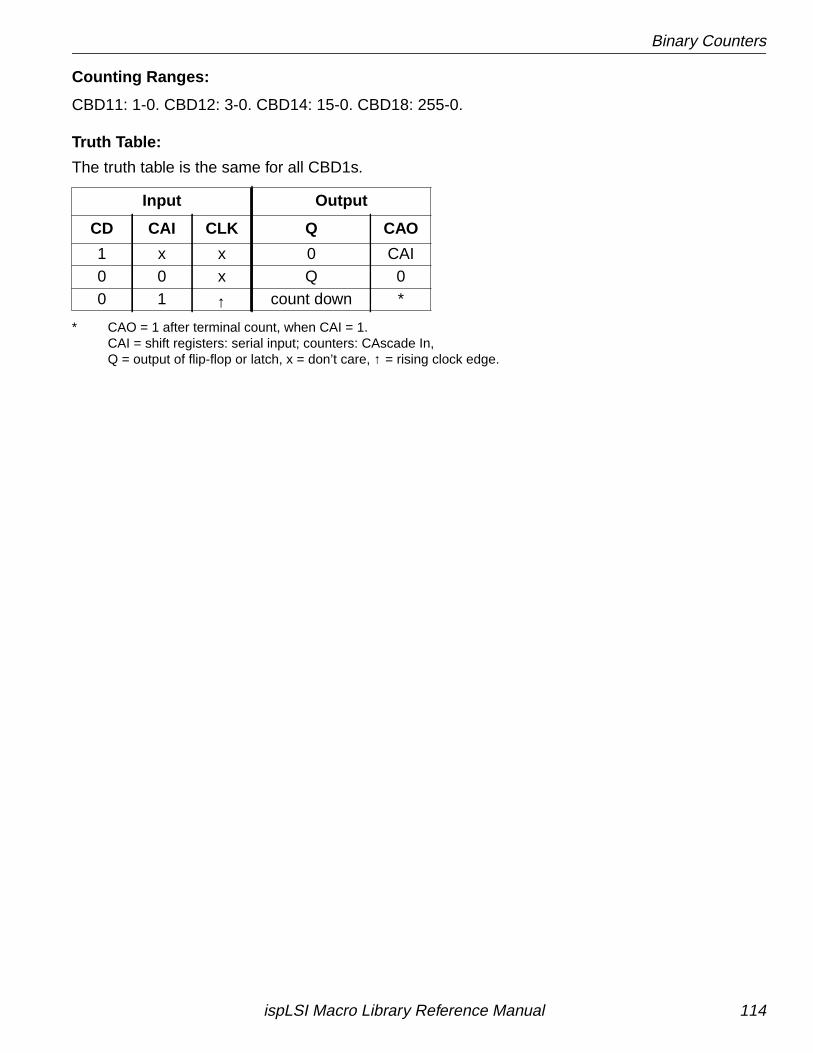
Binary Counters
Counting Ranges:
CBD11: 1-0. CBD12: 3-0. CBD14: 15-0. CBD18: 255-0.
Truth Table:
The truth table is the same for all CBD1s.
* CAO = 1 after terminal count, when CAI = 1.CAI = shift registers: serial input; counters: CAscade In,Q = output of flip-flop or latch, x = don’t care, ↑ = rising clock edge.
Input Output
CD CAI CLK Q CAO
1 x x 0 CAI0 0 x Q 00 1 ↑ count down *
ispLSI Macro Library Reference Manual 114
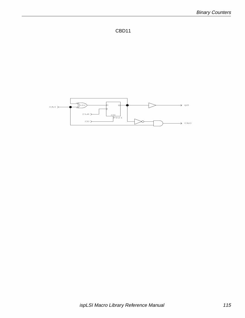
Binary Counters
Q0LX2
CLK
CDCAO
CAI
CD
QD
FD21
CBD11
ispLSI Macro Library Reference Manual 115
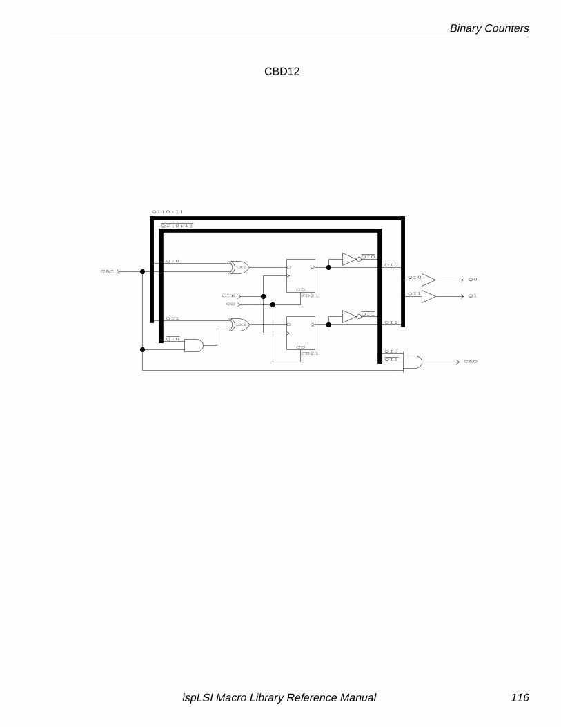
Binary Counters
Q1
Q0QI0
QI[0:1]
QI1
QI0
QI1
QI0
QI1
LX2
LX2
QI0
QI0
QI1
QI0
QI1
QI[0:1]
CLK
CD
CAI
CAO
CD
QD
FD21
CD
QD
FD21
CBD12
ispLSI Macro Library Reference Manual 116
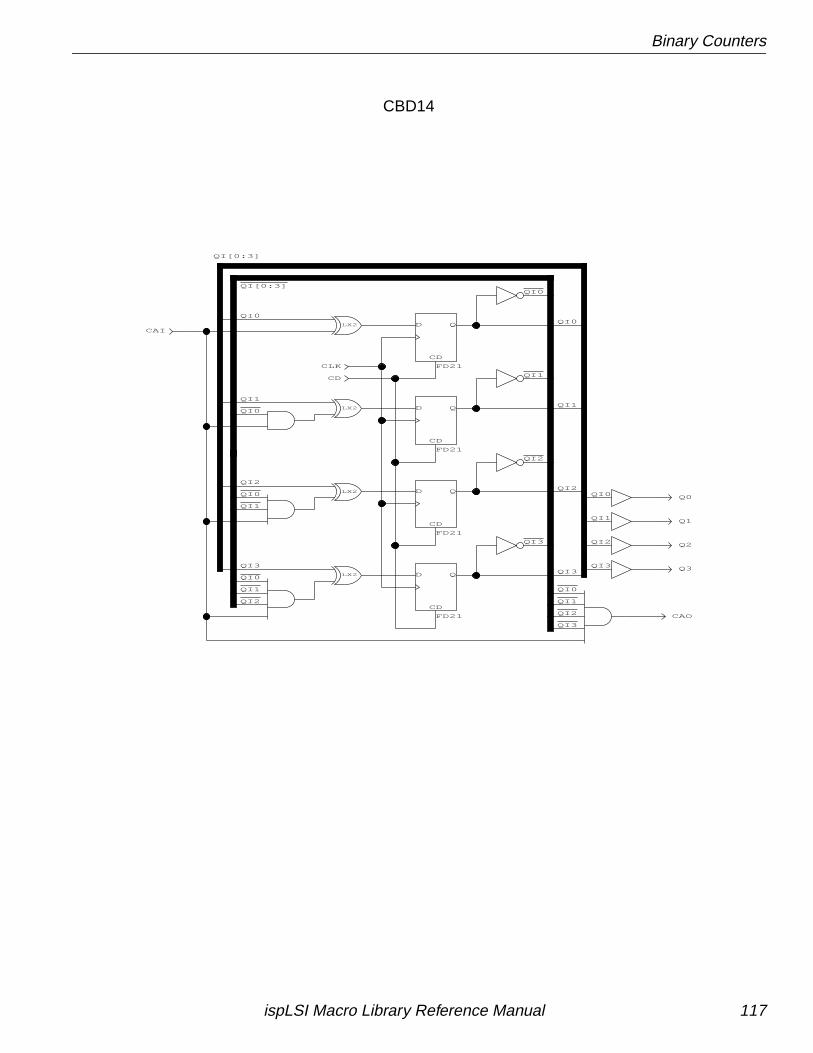
Binary Counters
Q3
Q2
Q1
Q0
QI3
QI2
QI1
QI0
QI2
QI[0:3]
QI1QI1
QI2
QI3
QI0QI0
QI3
QI2
QI[0:3]
QI0
QI0
QI1
QI1
QI2
QI3
QI3
QI1
QI0
QI0
QI1
QI2
QI0LX2
LX2
LX2
LX2
CLK
CD
CD
QD
FD21
CAO
CD
QD
FD21
CD
QD
FD21
CD
QD
FD21
CAI
CBD14
ispLSI Macro Library Reference Manual 117
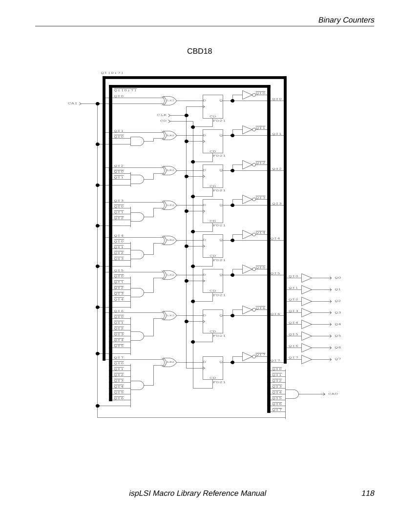
Binary Counters
Q3QI3
QI0QI5
QI4
QI[0:7]
QI0
QI2
QI3
QI4
QI5
QI6
QI7
QI1
QI0
QI1
QI2
QI3
QI6
QI7QI7
QI6
QI5
QI4
QI2
QI1
Q4
Q2
Q5
Q1
Q6
Q0
Q7
QI4
QI7
QI6
QI5
QI4
QI3
QI2
QI1
QI0
QI6
QI5
QI4
QI3
QI2
QI1
QI0
QI5
QI4
QI3
QI2
QI1
QI0
QI4
QI3
QI2
QI1
QI0
QI3
QI2
QI1
QI0
QI1
QI0
QI1
QI2
QI3
QI5
QI6
QI7
QI[0:7]
QI2
QI1
QI0
QI0
QI0
LX2
LX2
LX2
LX2
LX2
LX2
LX2
LX2
CD
CLK
CAI
CD
QD
FD21
CD
QD
FD21
CD
QD
FD21
CD
QD
FD21
CD
QD
FD21
CD
QD
FD21
CD
QD
FD21
CD
QD
FD21
CAO
CBD18
ispLSI Macro Library Reference Manual 118
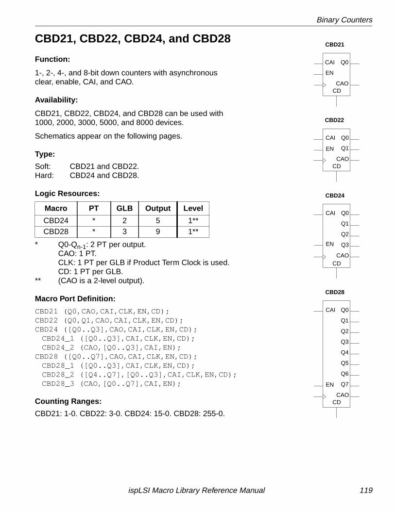
Binary Counters
CBD21, CBD22, CBD24, and CBD28
Function:
1-, 2-, 4-, and 8-bit down counters with asynchronousclear, enable, CAI, and CAO.
Availability:
CBD21, CBD22, CBD24, and CBD28 can be used with1000, 2000, 3000, 5000, and 8000 devices.
Schematics appear on the following pages.
Type:
Soft: CBD21 and CBD22.Hard: CBD24 and CBD28.
Logic Resources:
* Q0-Qn-1: 2 PT per output.CAO: 1 PT.CLK: 1 PT per GLB if Product Term Clock is used.CD: 1 PT per GLB.
** (CAO is a 2-level output).
Macro Port Definition:
CBD21 (Q0,CAO,CAI,CLK,EN,CD);CBD22 (Q0,Q1,CAO,CAI,CLK,EN,CD);CBD24 ([Q0..Q3],CAO,CAI,CLK,EN,CD);
CBD24_1 ([Q0..Q3],CAI,CLK,EN,CD);CBD24_2 (CAO,[Q0..Q3],CAI,EN);
CBD28 ([Q0..Q7],CAO,CAI,CLK,EN,CD);CBD28_1 ([Q0..Q3],CAI,CLK,EN,CD);CBD28_2 ([Q4..Q7],[Q0..Q3],CAI,CLK,EN,CD);CBD28_3 (CAO,[Q0..Q7],CAI,EN);
Counting Ranges:
CBD21: 1-0. CBD22: 3-0. CBD24: 15-0. CBD28: 255-0.
Macro PT GLB Output Level
CBD24 * 2 5 1**CBD28 * 3 9 1**
CBD21
CBD22
CBD24
CBD28
CDCAO
Q0CAI
CDCAO
Q1
Q0CAI
CDCAO
Q3
Q2
Q1
Q0CAI
Q7
Q6
Q5
Q4
Q3
Q2
Q1
Q0
CD
CAI
CAO
EN
EN
EN
EN
ispLSI Macro Library Reference Manual 119
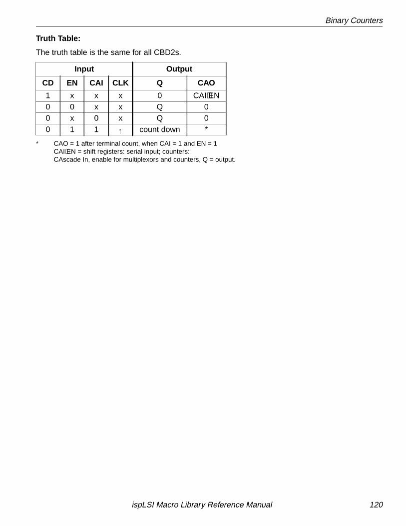
Binary Counters
Truth Table:
The truth table is the same for all CBD2s.
* CAO = 1 after terminal count, when CAI = 1 and EN = 1CAI⋅EN = shift registers: serial input; counters:CAscade In, enable for multiplexors and counters, Q = output.
Input Output
CD EN CAI CLK Q CAO
1 x x x 0 CAI⋅EN0 0 x x Q 00 x 0 x Q 00 1 1 ↑ count down *
ispLSI Macro Library Reference Manual 120
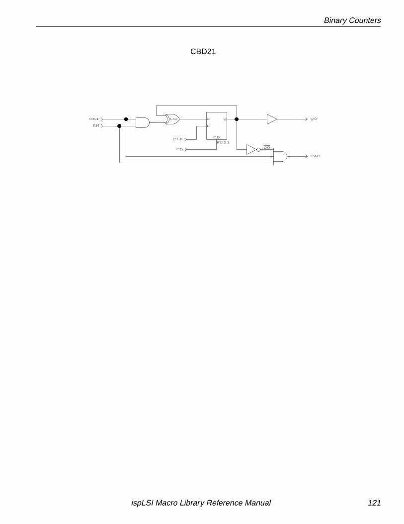
Binary Counters
Q0
CAO
LX2
CD
CLK
EN
CAI
CD
QD
FD21
Q0
CBD21
ispLSI Macro Library Reference Manual 121
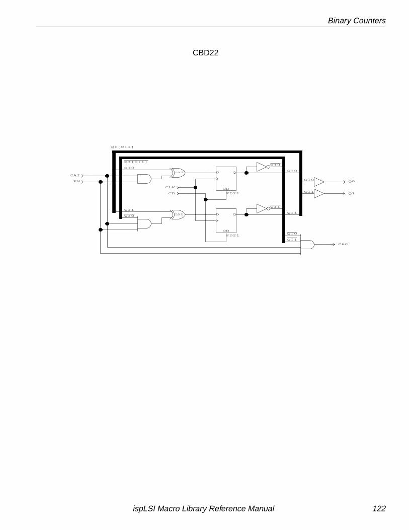
Binary Counters
Q1
Q0
QI[0:1]
QI1
QI0QI0
QI0
QI1
QI1
QI0
QI1
QI0
QI[0:1]
QI1
QI0
LX2
LX2
CLK
CD
EN
CAI
CD
QD
FD21
CD
QD
FD21
CAO
CBD22
ispLSI Macro Library Reference Manual 122
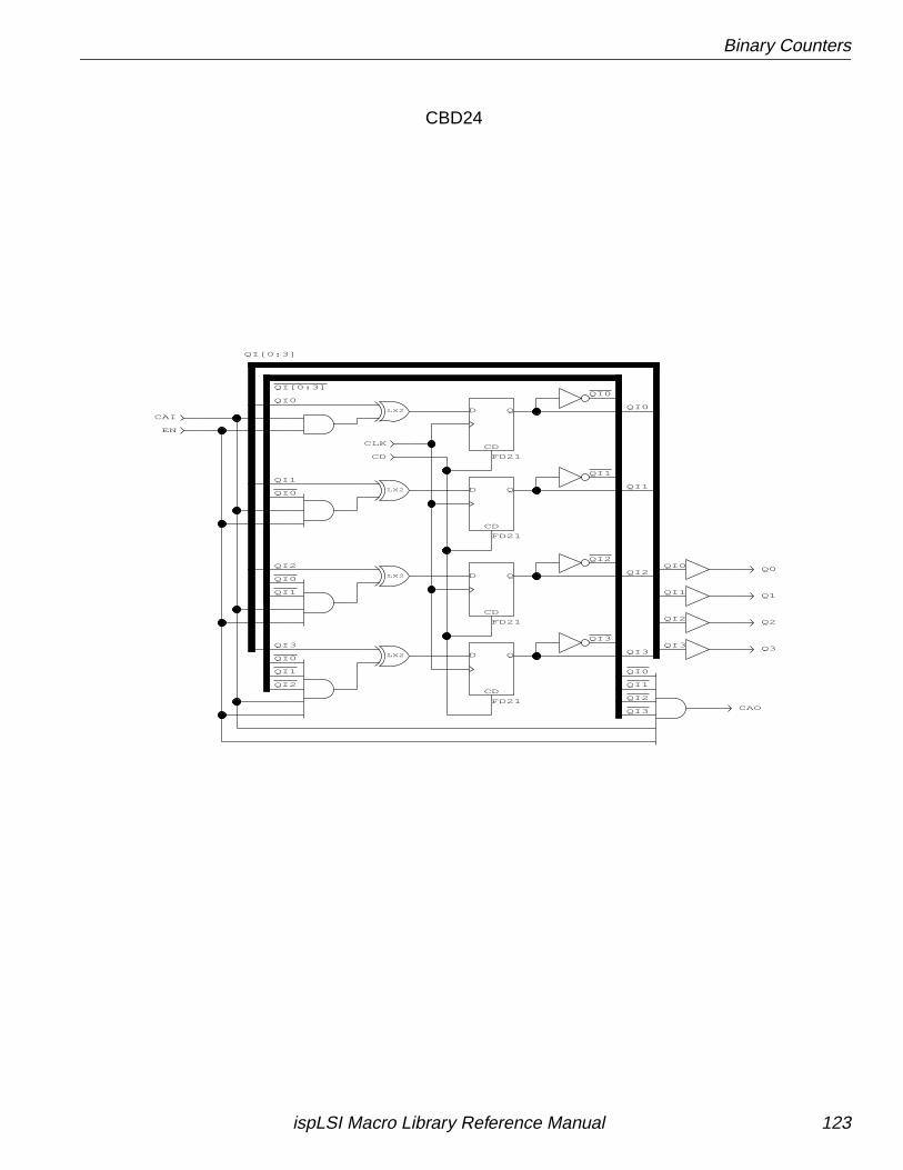
Binary Counters
QI3
QI2
QI[0:3]
QI0
QI1
QI2
QI3
QI0
QI2
QI1
QI0
QI1
QI0
QI0
QI1
Q0QI0
QI[0:3]
QI1
QI3
QI2
QI0QI0
QI1
QI3QI3
QI2
QI1
QI2
Q1
Q2
Q3LX2
LX2
LX2
LX2
CLK
CD
EN
CAI
CD
QD
FD21
CD
QD
FD21
CD
QD
FD21
CD
QD
FD21
CAO
CBD24
ispLSI Macro Library Reference Manual 123
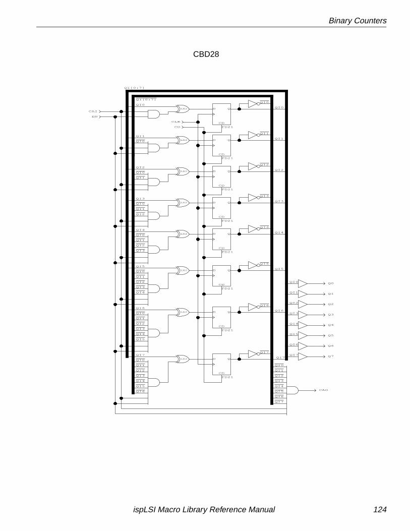
Binary Counters
Q5
Q4
Q3
Q2
Q1
Q0
Q6
Q7
QI5
QI2
QI2
QI0
QI0
QI1
QI3
QI4
QI6
QI7
QI3
QI2
QI1
QI5
QI4
QI3
QI2
QI1
QI0
QI4
QI3
QI2
QI1
QI0
QI3
QI2
QI0
QI2
QI1
QI0
QI1
QI0
QI0
QI5
QI6
QI7
QI0
QI1
QI3
QI4
QI5
QI6
QI[0:7]
QI1
QI4
CAO
CLK
CD
QD
FD21
CD
QD
FD21
CD
QD
FD21
CD
QD
FD21
CD
QD
FD21
CD
QD
FD21
CD
QD
FD21
CD
QD
FD21
EN
CAI
CD
LX2
LX2
LX2
LX2
LX2
LX2
LX2
LX2QI4
QI7
QI6
QI5
QI4
QI3
QI2
QI1
QI0
QI[0:7]
QI0
QI1
QI2
QI3
QI5
QI6
QI7QI7
QI6
QI5
QI4
QI3
QI2
QI1
QI0
CBD28
ispLSI Macro Library Reference Manual 124

Binary Counters
CBD31, CBD32, CBD34, and CBD38
Function:
1-, 2-, 4-, and 8-bit down counters with asynchronousclear, enable, parallel data load, synchronous preset, CAI,and CAO.
Availability:
CBD31, CBD32, CBD34, and CBD38 can be used with1000, 2000, 3000, 5000, and 8000 devices.
Schematics appear on the following pages.
Type:
Soft: CBD31 and CBD32.Hard: CBD34 and CBD38.
Logic Resources:
* Q0-Qn-1: 4 PT per output.CAO: 1 PT.CLK: 1 PT per GLB if Product Term Clock is used.CD: 1 PT per GLB.
** (CAO is a 2-level output).
Macro Port Definition:
CBD31 (Q0,CAO,D0,CAI,CLK,PS,LD,EN,CD);CBD32 (Q0,Q1,CAO,D0,D1,CAI,CLK,PS,LD,EN,CD);CBD34 ([Q0..Q3],CAO,[D0..D3],CAI,CLK,PS,LD,EN,CD);
CBD34_1 ([Q0..Q3],[D0..D3],CAI,CLK,PS,LD,EN,CD);CBD34_2 (CAO,[Q0..Q3],CAI,EN);
CBD38 ([Q0..Q7],CAO,[D0..D7],CAI,CLK,PS,LD,EN,CD);CBD38_1 ([Q0..Q3],[D0..D3],CAI,CLK,PS,LD,EN,CD);CBD38_2 (Q4,Q5,[Q0..Q3],D4,D5,CAI,CLK,PS,LD,EN,CD);CBD38_3 (Q6,Q7,[Q0..Q5],D6,D7,CAI,CLK,PS,LD,EN,CD);CBD38_4 (CAO,[Q0..Q7],CAI,EN);
Counting Ranges:
CBD31: 1-0. CBD32: 3-0. CBD34: 15-0. CBD38: 255-0.
Macro PT GLB Output Level
CBD34 * 2 5 1**CBD38 * 3 9 1**
CBD31 CBD32
CBD34 CBD38
PS
Q0
CAO
EN
CAI
LD
D0
CD
D0
1
LD
CAI
EN
Q1
CAO
Q0
PS
CD
PS
Q0
CAO
Q1
Q2
Q3
EN
CAI
LD
D3
D2
D1
D0
CD
PS
D0
D1
D2
D3
D4
D5
D6
LD
D7
CAI
EN
Q7
Q6
Q5
Q4
Q3
Q2
Q1
CAO
Q0
CD
ispLSI Macro Library Reference Manual 125
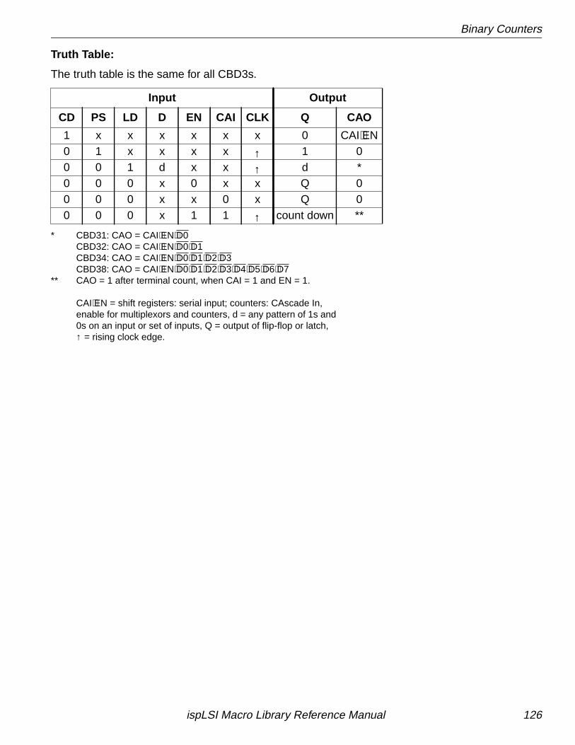
Binary Counters
Truth Table:
The truth table is the same for all CBD3s.
* CBD31: CAO = CAI⋅EN⋅D0CBD32: CAO = CAI⋅EN⋅D0⋅D1CBD34: CAO = CAI⋅EN⋅D0⋅D1⋅D2⋅D3CBD38: CAO = CAI⋅EN⋅D0⋅D1⋅D2⋅D3⋅D4⋅D5⋅D6⋅D7
** CAO = 1 after terminal count, when CAI = 1 and EN = 1.
CAI⋅EN = shift registers: serial input; counters: CAscade In,enable for multiplexors and counters, d = any pattern of 1s and0s on an input or set of inputs, Q = output of flip-flop or latch,↑ = rising clock edge.
Input Output
CD PS LD D EN CAI CLK Q CAO
1 x x x x x x 0 CAI⋅EN0 1 x x x x ↑ 1 00 0 1 d x x ↑ d *0 0 0 x 0 x x Q 00 0 0 x x 0 x Q 00 0 0 x 1 1 ↑ count down **
ispLSI Macro Library Reference Manual 126
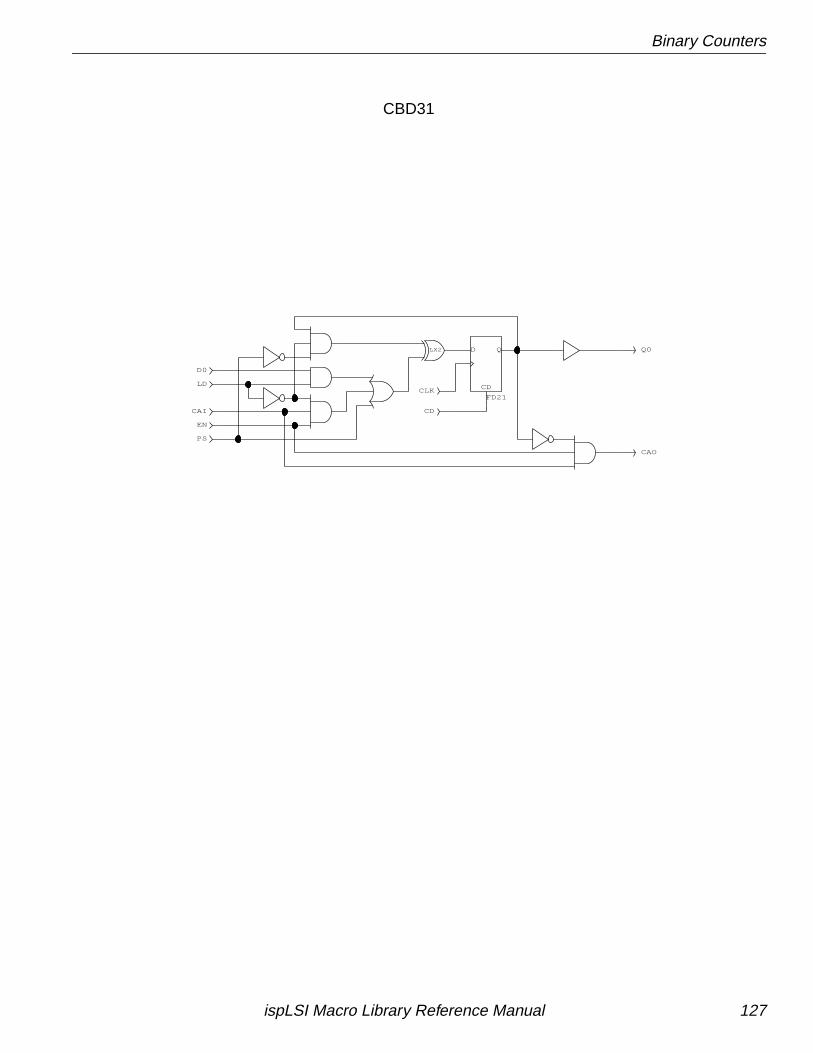
Binary Counters
Q0LX2
CAO
CD
CLK
PS
EN
CAI
LD
D0
CD
QD
FD21
CBD31
ispLSI Macro Library Reference Manual 127
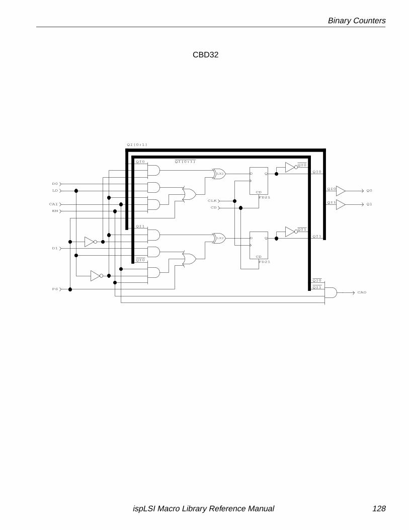
Binary Counters
Q0
Q1
QI0
QI1
QI1
QI0
QI1
QI[0:1]
QI0
QI1
QI[0:1]QI0
QI0
QI1
QI0
LX2
LX2
CAI
LD
D0
EN
D1
PS
CD
QD
FD21
CD
QD
FD21
CD
CLK
CAO
CBD32
ispLSI Macro Library Reference Manual 128
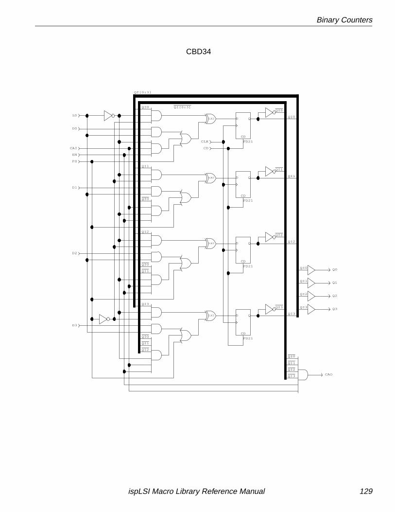
Binary Counters
QI[0:3]
QI3
QI0
QI0
QI0
QI1
QI0
QI1
QI2
QI0
QI1
QI2
QI3
QI1
QI2
Q3
Q2
Q1
Q0QI0
QI1
QI2
QI3
QI3
QI2
QI1
QI0
QI[0:3]
QI0
QI1
QI2
QI3
LX2
LX2
LX2
LX2
CD
PS
EN
CAI
LD
D2
D3
CD
QD
FD21
CD
QD
FD21
CD
QD
FD21
CD
QD
FD21
D1
D0
CLK
CAO
CBD34
ispLSI Macro Library Reference Manual 129
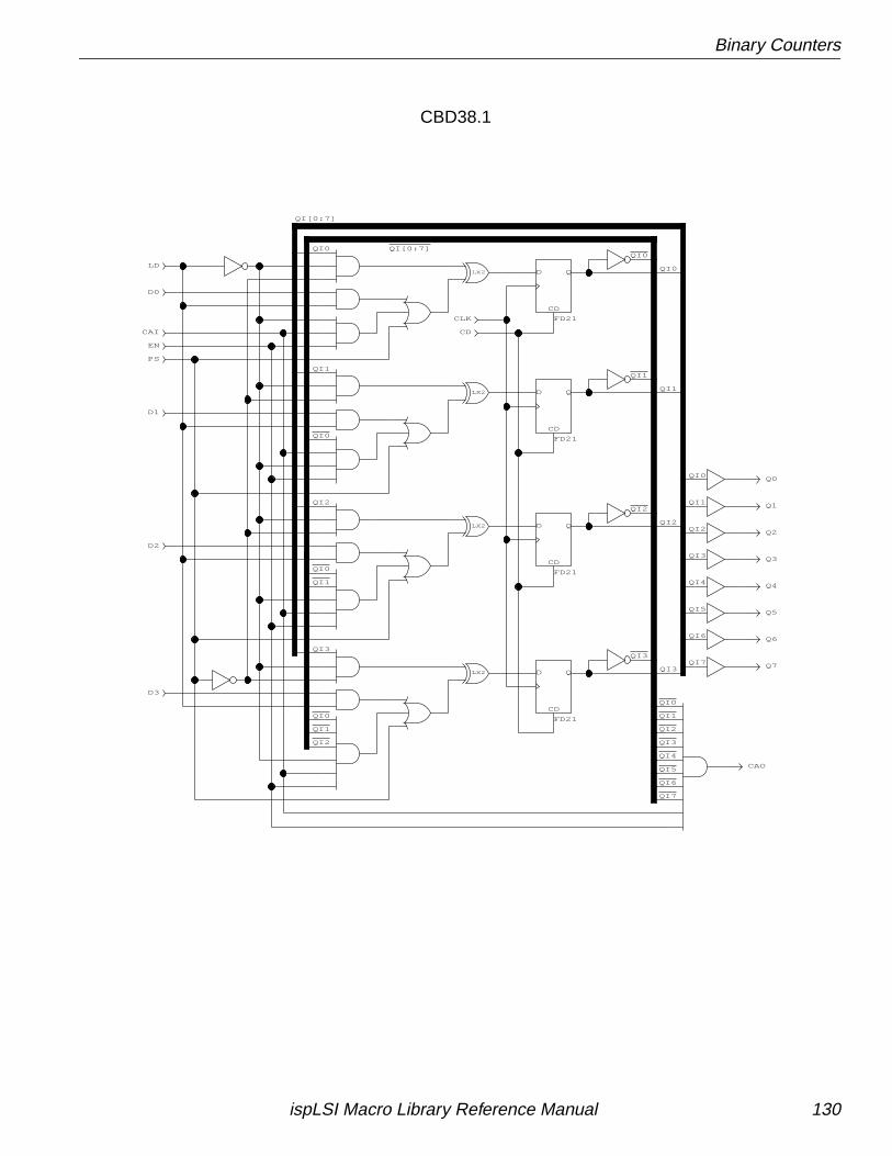
Binary Counters
QI3
QI2QI2
QI3
QI4
QI5
QI6
QI7
QI0
QI1
QI[0:7]
QI2
QI3
QI1
QI0
QI0
QI1
QI0
QI3
QI0
QI1
QI2
QI3
QI4
QI5
QI6
QI7
QI2
QI1
QI0
QI1
QI0
QI1
QI2
QI0
QI[0:7]
CAO
CD
PS
EN
CAI
LD
D0
D1
D2
D3
CD
QD
FD21
CD
QD
FD21
CD
QD
FD21
CD
QD
FD21
CLK
LX2
LX2
LX2
LX2Q7
Q6
Q5
Q4
Q3
Q2
Q1
Q0
CBD38.1
ispLSI Macro Library Reference Manual 130
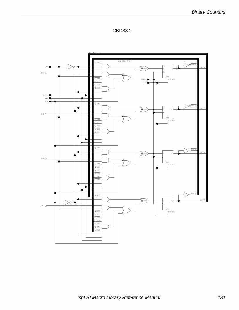
Binary Counters
QI7
QI6
QI5
QI4
QI[0:7]
QI4
QI5
QI7
QI6
QI4
QI7
QI6
QI5
QI[0:7]
QI0
QI1
QI2
QI0
QI1
QI2
QI3
QI0
QI1
QI2
QI3
QI4
QI0
QI1
QI2
QI6
QI5
QI4
QI3
QI5
QI4
QI3
LX2
LX2
LX2
LX2
D4
D5
D6
D7
CD
CLK
CD
QD
FD21
CD
QD
FD21
CD
QD
FD21
CD
QD
FD21
CAI
EN
PS
LD
CBD38.2
ispLSI Macro Library Reference Manual 131
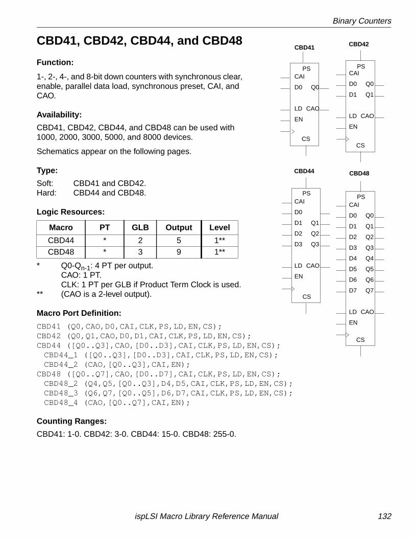
Binary Counters
CBD41, CBD42, CBD44, and CBD48
Function:
1-, 2-, 4-, and 8-bit down counters with synchronous clear,enable, parallel data load, synchronous preset, CAI, andCAO.
Availability:
CBD41, CBD42, CBD44, and CBD48 can be used with1000, 2000, 3000, 5000, and 8000 devices.
Schematics appear on the following pages.
Type:
Soft: CBD41 and CBD42.Hard: CBD44 and CBD48.
Logic Resources:
* Q0-Qn-1: 4 PT per output.CAO: 1 PT.CLK: 1 PT per GLB if Product Term Clock is used.
** (CAO is a 2-level output).
Macro Port Definition:
CBD41 (Q0,CAO,D0,CAI,CLK,PS,LD,EN,CS);CBD42 (Q0,Q1,CAO,D0,D1,CAI,CLK,PS,LD,EN,CS);CBD44 ([Q0..Q3],CAO,[D0..D3],CAI,CLK,PS,LD,EN,CS);
CBD44_1 ([Q0..Q3],[D0..D3],CAI,CLK,PS,LD,EN,CS);CBD44_2 (CAO,[Q0..Q3],CAI,EN);
CBD48 ([Q0..Q7],CAO,[D0..D7],CAI,CLK,PS,LD,EN,CS);CBD48_2 (Q4,Q5,[Q0..Q3],D4,D5,CAI,CLK,PS,LD,EN,CS);CBD48_3 (Q6,Q7,[Q0..Q5],D6,D7,CAI,CLK,PS,LD,EN,CS);CBD48_4 (CAO,[Q0..Q7],CAI,EN);
Counting Ranges:
CBD41: 1-0. CBD42: 3-0. CBD44: 15-0. CBD48: 255-0.
Macro PT GLB Output Level
CBD44 * 2 5 1**CBD48 * 3 9 1**
CBD41 CBD42
CBD44 CBD48
PS
Q0
CAO
EN
CAI
LD
D0
CS
D0
D1
LD
CAI
EN
Q1
CAO
Q0
PS
CS
PS
CAO
Q1
Q2
Q3
EN
CAI
LD
D3
D2
D1
D0
CS
PS
D0
D1
D2
D3
D4
D5
D6
LD
D7
CAI
EN
Q7
Q6
Q5
Q4
Q3
Q2
Q1
CAO
Q0
CS
ispLSI Macro Library Reference Manual 132
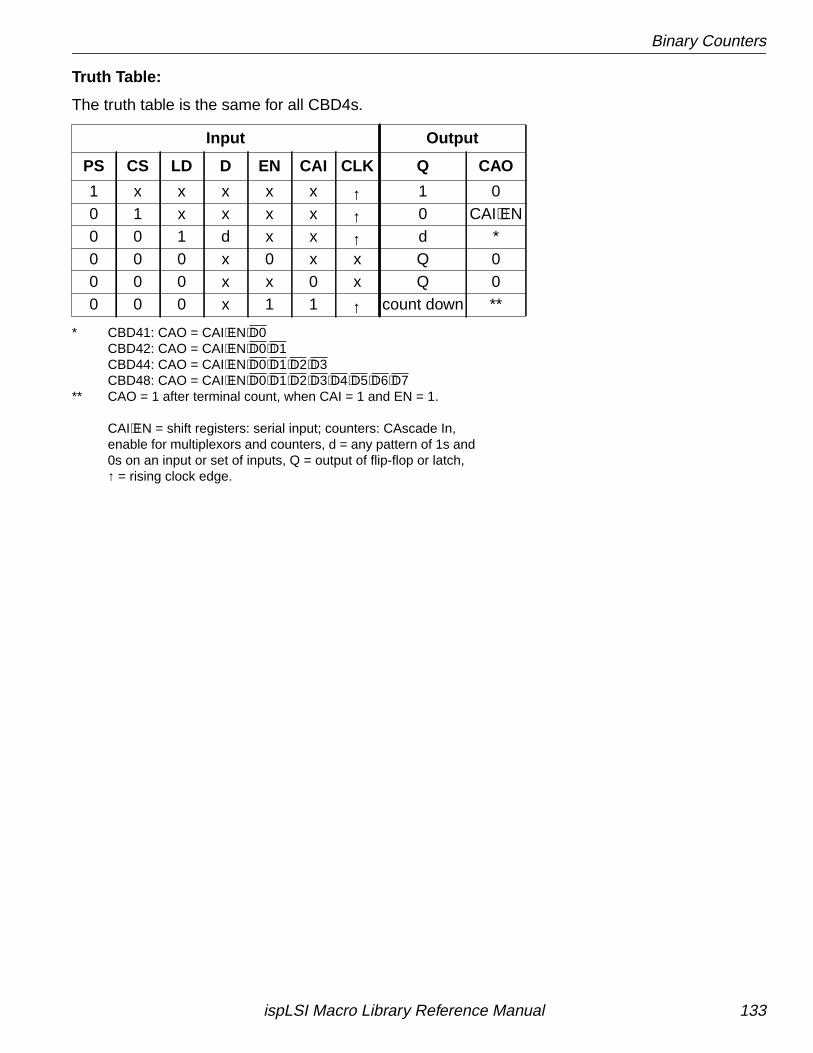
Binary Counters
Truth Table:
The truth table is the same for all CBD4s.
* CBD41: CAO = CAI⋅EN⋅D0CBD42: CAO = CAI⋅EN⋅D0⋅D1CBD44: CAO = CAI⋅EN⋅D0⋅D1⋅D2⋅D3CBD48: CAO = CAI⋅EN⋅D0⋅D1⋅D2⋅D3⋅D4⋅D5⋅D6⋅D7
** CAO = 1 after terminal count, when CAI = 1 and EN = 1.
CAI⋅EN = shift registers: serial input; counters: CAscade In,enable for multiplexors and counters, d = any pattern of 1s and0s on an input or set of inputs, Q = output of flip-flop or latch,↑ = rising clock edge.
Input Output
PS CS LD D EN CAI CLK Q CAO
1 x x x x x ↑ 1 00 1 x x x x ↑ 0 CAI⋅EN0 0 1 d x x ↑ d *0 0 0 x 0 x x Q 00 0 0 x x 0 x Q 00 0 0 x 1 1 ↑ count down **
ispLSI Macro Library Reference Manual 133
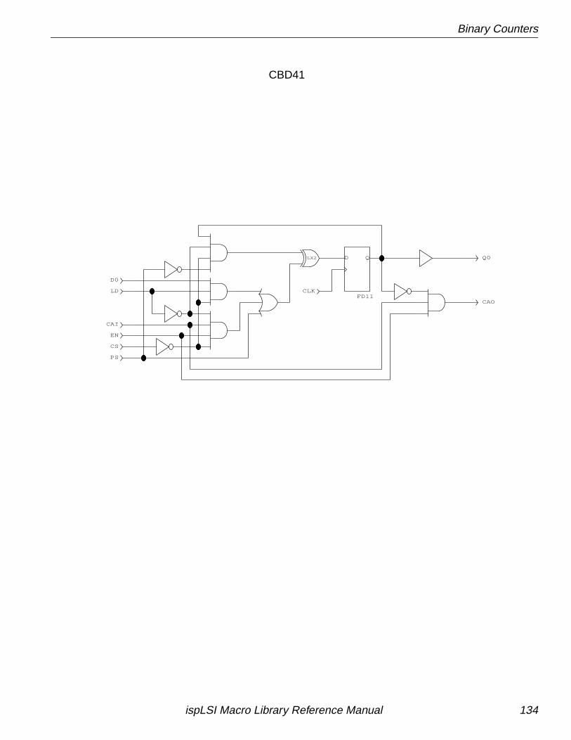
Binary Counters
Q0LX2 QD
FD11CLK
CAO
PS
CS
EN
CAI
LD
D0
CBD41
ispLSI Macro Library Reference Manual 134
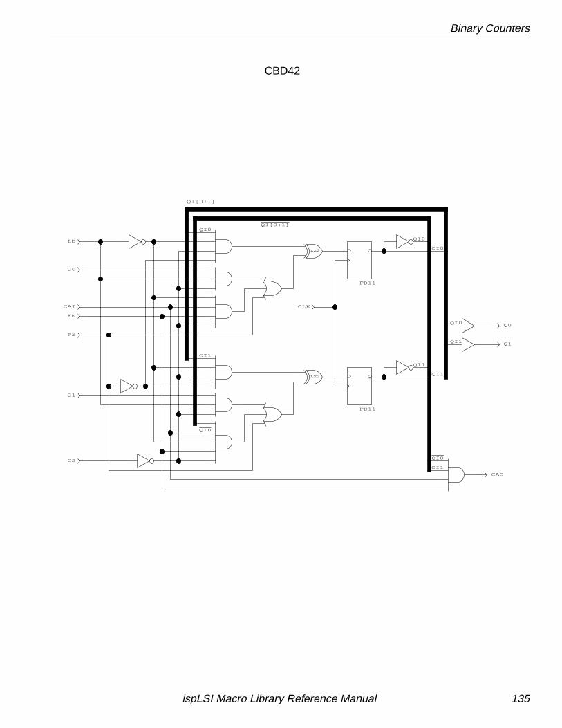
Binary Counters
Q1
Q0QI0
QI1
QI[0:1]
QI0
QI1
QI0
QI1
QI1
QI0
QI1
QI0
QI0
QI[0:1]
LX2
LX2
CS
D1
PS
EN
CAI
D0
LD
QD
FD11
QD
FD11
CLK
CAO
CBD42
ispLSI Macro Library Reference Manual 135
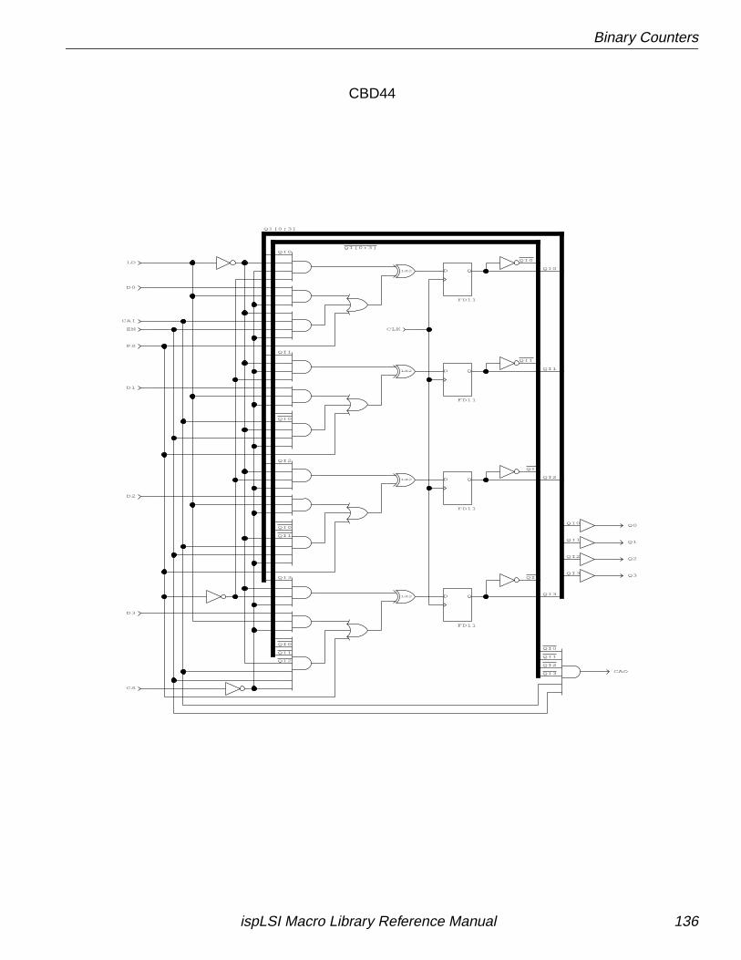
Binary Counters
Q0
Q1
Q2
Q3
QI0
QI2
QI3
QI1
QI0
QI3
QI2
QI1
QI[0:3]
QI2
QI3
QI0
QI1
QI2
QI1
QI[0:3]
QI2
QI3
QI3
QI1
QI0
QI0
QI1
QI2
QI1
QI0
QI0
QI0
LX2
LX2
LX2
LX2
CAI
EN
PS
CS
D3
D2
D1
D0
LD
CLK
QD
FD11
QD
FD11
QD
FD11
QD
FD11
CAO
CBD44
ispLSI Macro Library Reference Manual 136
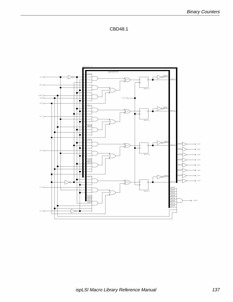
Binary Counters
Q0
Q1
Q2
Q3QI3
QI2
QI1
QI0
QI[0:7]
QI2
QI3
QI1
QI0
QI0
QI1
QI4
QI5
QI6
QI3QI7
QI2
Q4
Q5
Q6
Q7
QI1
QI4
QI7
QI6
QI5
QI[0:7]
QI2
QI3
QI0
QI1
QI2
QI1
QI0
QI0
QI0
QI2
QI1
QI0
QI3
LX2
LX2
LX2
LX2
QD
FD11
QD
FD11
QD
FD11
QD
FD11
CLK
LD
D0
D1
D2
D3
CS
PS
EN
CAI
CAO
CBD48.1
ispLSI Macro Library Reference Manual 137
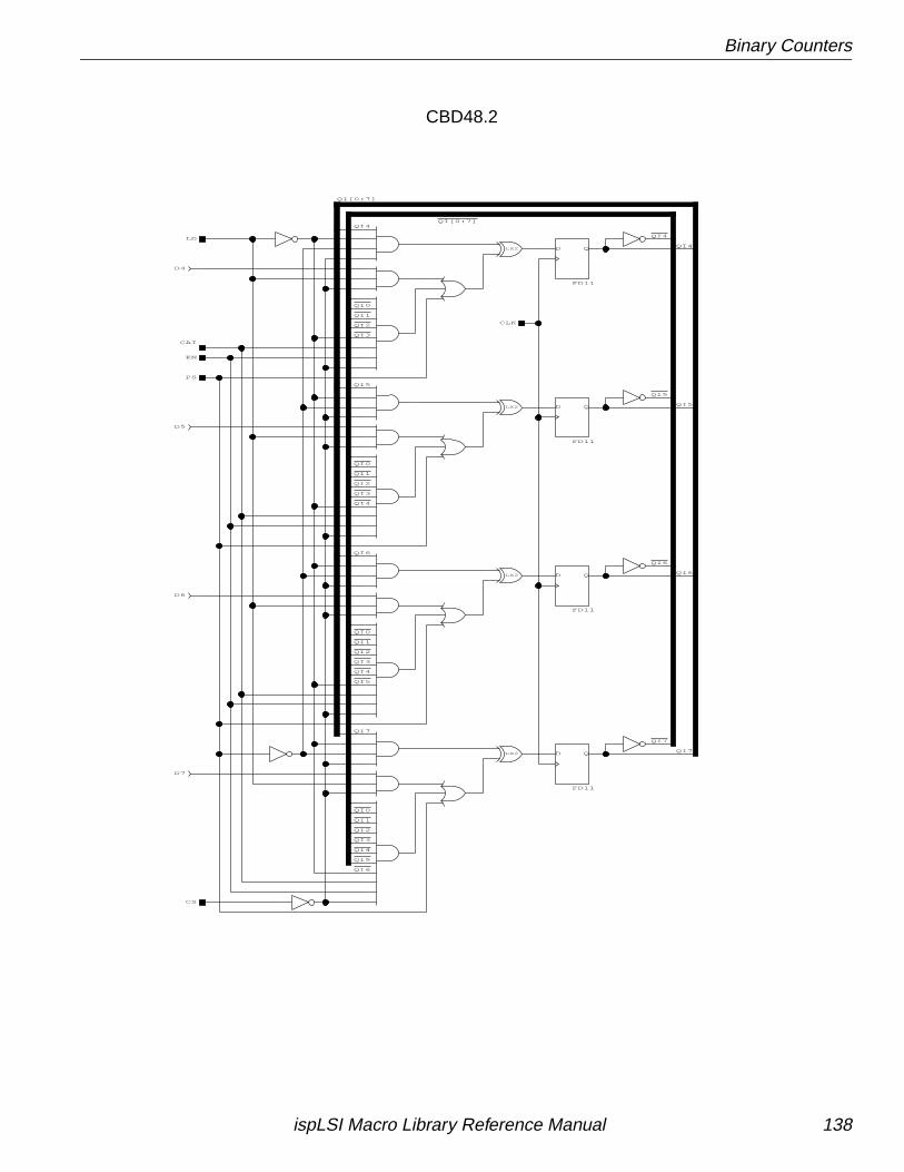
Binary Counters
QI0
QI7
QI6
QI5
QI[0:7]
QI2
QI0
QI1
QI2
QI3
QI4
QI5
QI6
QI5
QI4
QI3
QI1
QI4
QI0
QI1
QI2
QI3
QI0
QI1
QI2
QI3
QI4
PS
LX2
LX2
LX2
LX2
LD
D4
D5
D6
D7
CS
CLK
QD
FD11
QD
FD11
QD
FD11
QD
FD11
EN
CAI
QI5
QI4
QI6
QI7
QI[0:7]
QI4
QI5
QI6
QI7
CBD48.2
ispLSI Macro Library Reference Manual 138
Binary Counters
CBD516 and CBD616
Function:
16-bit down counters with asynchronous clear andenable. CBD616 also has CAO.
Availability:
CBD516 and CBD616 can be used with 1000, 2000,3000, 5000, and 8000 devices.
Schematics appear on the following pages.
Type: Hard
Logic Resources:
* Q0-Qn-1: 2 PT per output.CLK: 1 PT per GLB if Product Term Clock is used.CD: 1 PT per GLB.
** Q0-Qn-1: 2 PT per output.CAO: 1 PT.CLK: 1 PT per GLB if Product Term Clock is used.CD: 1 PT per GLB.
*** (CAO is a 2-level output).
Macro Port Definition:
CBD516 ([Q0..Q15],CLK,EN,CD);CBD516_1 ([Q0..Q3],CLK,EN,CD);CBD516_2 ([Q4..Q7],[Q0..Q3],CLK,EN,CD);CBD516_3 ([Q8..Q11],[Q0..Q7],CLK,EN,CD);CBD516_4 ([Q12..Q15],[Q0..Q11],CLK,EN,CD);
CBD616 ([Q0..Q15],CAO,CLK,EN,CD);CBD616_1 ([Q0..Q3],CLK,EN,CD);CBD616_2 ([Q4..Q7],[Q0..Q3],CLK,EN,CD);CBD616_3 ([Q8..Q11],[Q0..Q7],CLK,EN,CD);CBD616_4 (Q12,Q13,[Q0..Q11],CLK,EN,CD);CBD616_5 (Q14,Q15,CAO,[Q0..Q13],CLK,EN,CD);
Counting Ranges:
CBD516: 65,535-0. CBD616: 65,535-0.
Macro PT GLB Output Level
CBD516 * 4 16 1CBD616 ** 5 18 2***
CBD516
CBD616
Q0
Q1
Q2
Q3
Q4
Q5
Q6
Q7
Q8
Q10
Q11
Q12
Q13
Q14
CD
Q15
Q9
EN
EN
Q9
Q15
CAO
CD
Q14
Q13
Q12
Q11
Q10
Q8
Q7
Q6
Q5
Q4
Q3
Q2
Q1
Q0
ispLSI Macro Library Reference Manual 139

Binary Counters
Truth Table:
Gray areas (CAO) apply only to the CBD616.
* CAO = 1 after terminal count, when EN = 1 and terminal count = 0.EN = enable for multiplexors and counters,Q = output of flip-flop or latch, x = don’t care,↑ = rising clock edge.
Input Output
CD EN CLK Q CAO
1 x x 0 EN0 0 x Q 00 1 ↑ count down *
ispLSI Macro Library Reference Manual 140
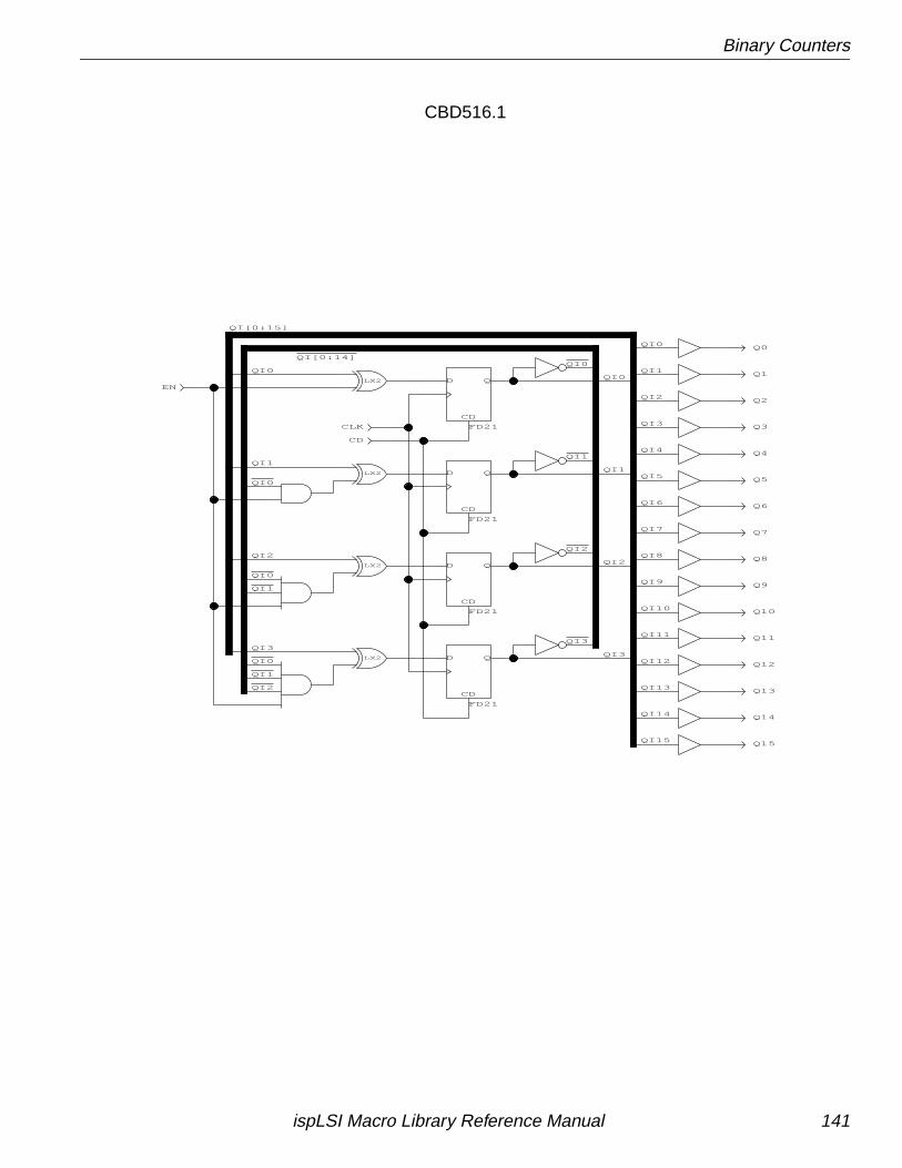
Binary Counters
Q9
LX2
LX2
LX2
LX2
CD
CLK
CD
QD
FD21
CD
QD
FD21
CD
QD
FD21
CD
QD
FD21
QI1
QI0
QI1
QI0
QI1
QI2
QI0
QI2
QI[0:14]
QI0
QI3
EN
Q3
Q2
Q1
Q0
Q8
Q7
Q6
Q5
Q4
QI12
QI13
QI14
QI15
QI11
QI10
QI9
QI2QI8
QI7
QI3
QI1
QI0
QI0
QI1
QI2
QI3
QI[0:15]
QI0
QI2
QI4
QI1QI5
QI6
QI3
Q15
Q14
Q13
Q12
Q11
Q10
CBD516.1
ispLSI Macro Library Reference Manual 141
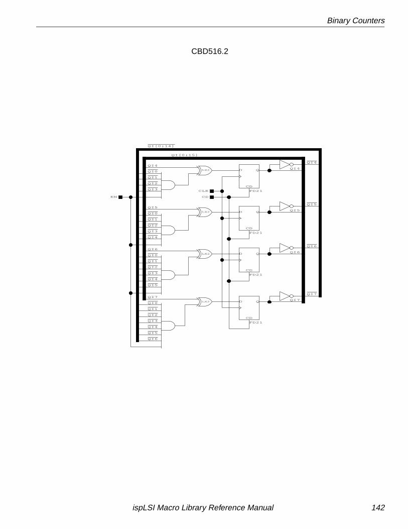
Binary Counters
QI6
QI6
QI4
QI4
QI0
QI1
QI2
QI3
QI5
QI7
QI0
QI1
QI2
QI3
QI4
QI5
QI0
QI1
QI2
QI3
QI4
QI5
QI0
QI1
QI2
QI3
QI[0:14]
QI6
QI4
QI7
QI[0:15]
QI6
QI5
QI4
QI5
QI7
EN
CD
QD
FD21
CD
QD
FD21
CD
QD
FD21
CD
QD
FD21
CD
CLK
LX2
LX2
LX2
LX2
CBD516.2
ispLSI Macro Library Reference Manual 142

Binary Counters
QI11
QI9QI9
QI8
QI[0:15]
QI8
QI10QI10
QI11
QI0
QI0
QI1
QI3
QI2
QI4
QI5
QI6
QI8
QI[0:14]
QI11
QI10
QI1
QI2
QI3
QI4
QI5
QI6
QI7
QI9
QI8
QI7
QI6
QI5
QI4
QI3
QI2
QI1
QI0
QI9
QI9
QI3
QI2
QI1
QI0
QI4
QI5
QI6
QI7
QI8
QI7
QI10
QI8
EN
CD
QD
FD21
CD
QD
FD21
CD
QD
FD21
CD
QD
FD21
CLK
CD
LX2
LX2
LX2
LX2
CBD516.3
ispLSI Macro Library Reference Manual 143
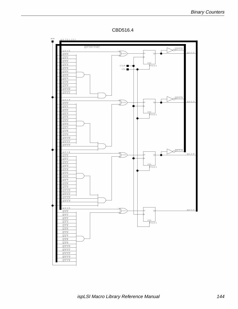
Binary Counters
QI13
QI12
QI14
QI12
QI13
QI14
QI15
QI[0:15]
QI15
QI9
QI3
QI5
QI12
QI2
QI[0:14]
QI0
QI1
QI2
QI4
QI5
QI6
QI7
QI8
QI10
QI11
QI12
QI13
QI14
QI13
QI12
QI11
QI10
QI9
QI8
QI7
QI6
QI4
QI3
QI2
QI1
QI0
QI14
QI13
QI12
QI0
QI1
QI3
QI4
QI5
QI6
QI7
QI8
QI9
QI10
QI11
QI0
QI1
QI2
QI3
QI4
QI5
QI6
QI7
QI8
QI9
QI10
QI11
EN
CLK
CD
CD
QD
FD21
CD
QD
FD21
CD
QD
FD21
CD
QD
FD21
LX2
LX2
LX2
LX2
CBD516.4
ispLSI Macro Library Reference Manual 144
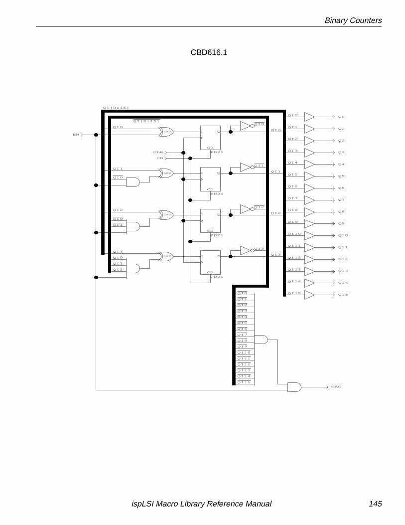
Binary Counters
Q15
Q14
Q13
Q12
Q11
Q10
Q9
QI13
QI15
QI14
QI3
QI11
QI10
QI8
QI7
QI6
QI1
QI0
QI[0:15]
QI0
QI1
QI2
QI3
QI0
QI2
QI3
QI4
QI1QI5
QI2
QI9
QI12
Q4
Q5
Q6
Q7
Q8
Q0
Q1
Q2
Q3
QI2
QI0
QI0
QI1
QI[0:15]QI0
QI1
QI3
QI2
QI0
QI1
QI0
QI1
QI2
QI3
QI4
QI5
QI6
QI7
QI8
QI9
QI10
QI11
QI12
QI13
QI14
QI15
EN
LX2
LX2
LX2
LX2
CD
QD
FD21
CD
QD
FD21
CD
QD
FD21
CD
QD
FD21
CAO
CLK
CD
CBD616.1
ispLSI Macro Library Reference Manual 145
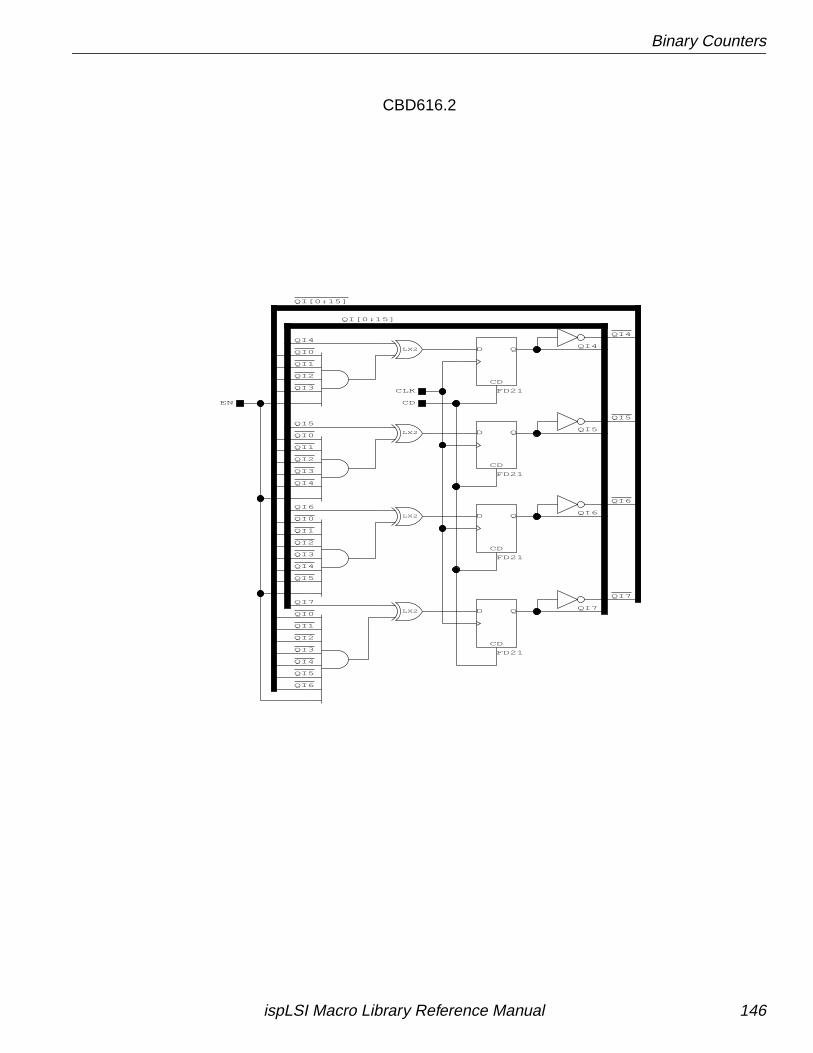
Binary Counters
QI6
QI4
QI3
QI4
QI2
QI3
QI0
QI1
QI2
QI4
QI5
QI6
QI7
QI0
QI1
QI2
QI3
QI5
QI0
QI1
QI3
QI4
QI5
QI0
QI1
QI2
QI[0:15]
QI6
QI5
QI4
QI[0:15]
QI7
QI6
QI5
QI4
QI7LX2
LX2
LX2
LX2
CD
QD
FD21
CD
QD
FD21
CD
QD
FD21
CD
QD
FD21
CD
CLK
EN
CBD616.2
ispLSI Macro Library Reference Manual 146
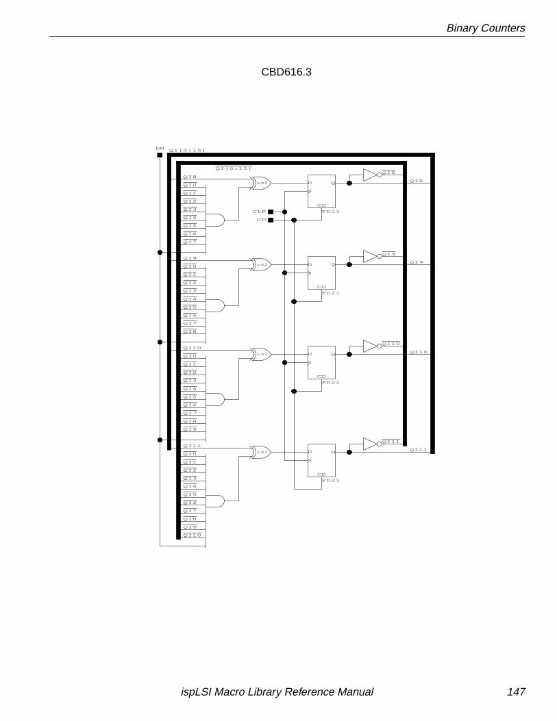
Binary Counters
QI8
QI9
QI[0:15]
QI10
QI9
QI8
QI11
QI10
QI11
QI9
QI[0:15]
QI0
QI1
QI3
QI2
QI4
QI5
QI6
QI7
QI8
QI11
QI10
QI0
QI1
QI2
QI3
QI4
QI5
QI6
QI7
QI8
QI10
QI9
QI8
QI7
QI6
QI5
QI4
QI3
QI2
QI1
QI0
QI3
QI2
QI1
QI0
QI4
QI5
QI6
QI7
QI8
QI9
LX2
LX2
LX2
LX2
EN
CD
QD
FD21
CD
QD
FD21
CD
QD
FD21
CD
QD
FD21
CLK
CD
CBD616.3
ispLSI Macro Library Reference Manual 147
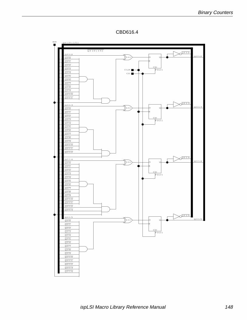
Binary Counters
QI13
QI12
QI14
QI12
QI13
QI14
QI15
QI[0:15]
QI15
EN
CLK
CD
CD
QD
FD21
CD
QD
FD21
CD
QD
FD21
CD
QD
FD21
LX2
LX2
LX2
LX2
QI15
QI0
QI1
QI2
QI3
QI4
QI5
QI6
QI7
QI8
QI9
QI10
QI11
QI0
QI1
QI2
QI3
QI4
QI5
QI6
QI7
QI8
QI9
QI10
QI11
QI12
QI5
QI0
QI1
QI2
QI3
QI4
QI5
QI6
QI7
QI8
QI9
QI10
QI11
QI12
QI13
QI14
QI13
QI12
QI11
QI10
QI9
QI8
QI7
QI6
QI4
QI3
QI2
QI1
QI0
QI[0:15]QI12
QI13
QI14
CBD616.4
ispLSI Macro Library Reference Manual 148
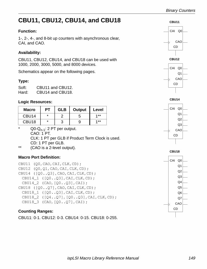
Binary Counters
CBU11, CBU12, CBU14, and CBU18
Function:
1-, 2-, 4-, and 8-bit up counters with asynchronous clear,CAI, and CAO.
Availability:
CBU11, CBU12, CBU14, and CBU18 can be used with1000, 2000, 3000, 5000, and 8000 devices.
Schematics appear on the following pages.
Type:
Soft: CBU11 and CBU12.Hard: CBU14 and CBU18.
Logic Resources:
* Q0-Qn-1: 2 PT per output.CAO: 1 PT.CLK: 1 PT per GLB if Product Term Clock is used.CD: 1 PT per GLB.
** (CAO is a 2-level output).
Macro Port Definition:
CBU11 (Q0,CAO,CAI,CLK,CD);CBU12 (Q0,Q1,CAO,CAI,CLK,CD);CBU14 ([Q0..Q3],CAO,CAI,CLK,CD);
CBU14_1 ([Q0..Q3],CAI,CLK,CD);CBU14_2 (CAO,[Q0..Q3],CAI);
CBU18 ([Q0..Q7],CAO,CAI,CLK,CD);CBU18_1 ([Q0..Q3],CAI,CLK,CD);CBU18_2 ([Q4..Q7],[Q0..Q3],CAI,CLK,CD);CBU18_3 (CAO,[Q0..Q7],CAI);
Counting Ranges:
CBU11: 0-1. CBU12: 0-3. CBU14: 0-15. CBU18: 0-255.
Macro PT GLB Output Level
CBU14 * 2 5 1**CBU18 * 3 9 1**
CBU11
CBU12
CBU14
CBU18
CD
CAO
Q0CAI
CD
CAO
Q1
Q0CAI
CD
CAO
Q3
Q2
Q1
Q0CAI
Q7
Q6
Q5
Q4
Q3
Q2
Q1
Q0
CD
CAI
CAO
ispLSI Macro Library Reference Manual 149
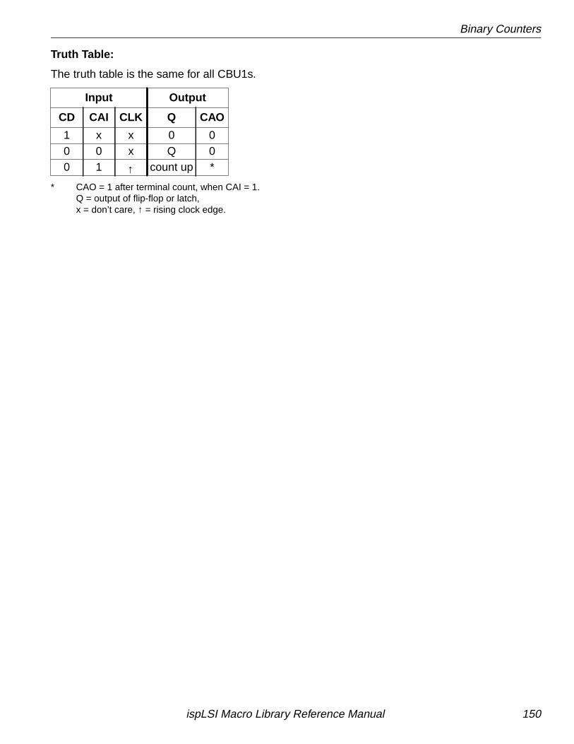
Binary Counters
Truth Table:
The truth table is the same for all CBU1s.
* CAO = 1 after terminal count, when CAI = 1.Q = output of flip-flop or latch,x = don’t care, ↑ = rising clock edge.
Input Output
CD CAI CLK Q CAO
1 x x 0 00 0 x Q 00 1 ↑ count up *
ispLSI Macro Library Reference Manual 150
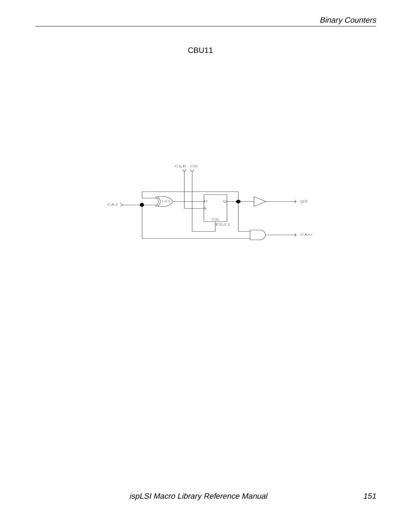
Binary Counters
LX2
CD
CAO
CD
QD
FD21
Q0CAI
CLK
CBU11
ispLSI Macro Library Reference Manual 151
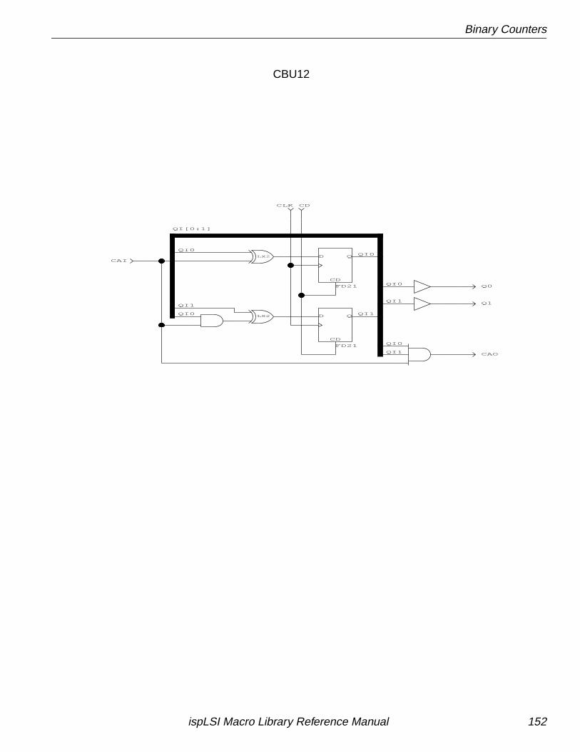
Binary Counters
QI1
QI0
QI1
QI0
QI1
QI0
QI[0:1]
QI0
QI0 QI1
Q0
LX2
LX2
CLK CD
CAI
Q1
CAO
CD
QD
FD21
CD
QD
FD21
CBU12
ispLSI Macro Library Reference Manual 152
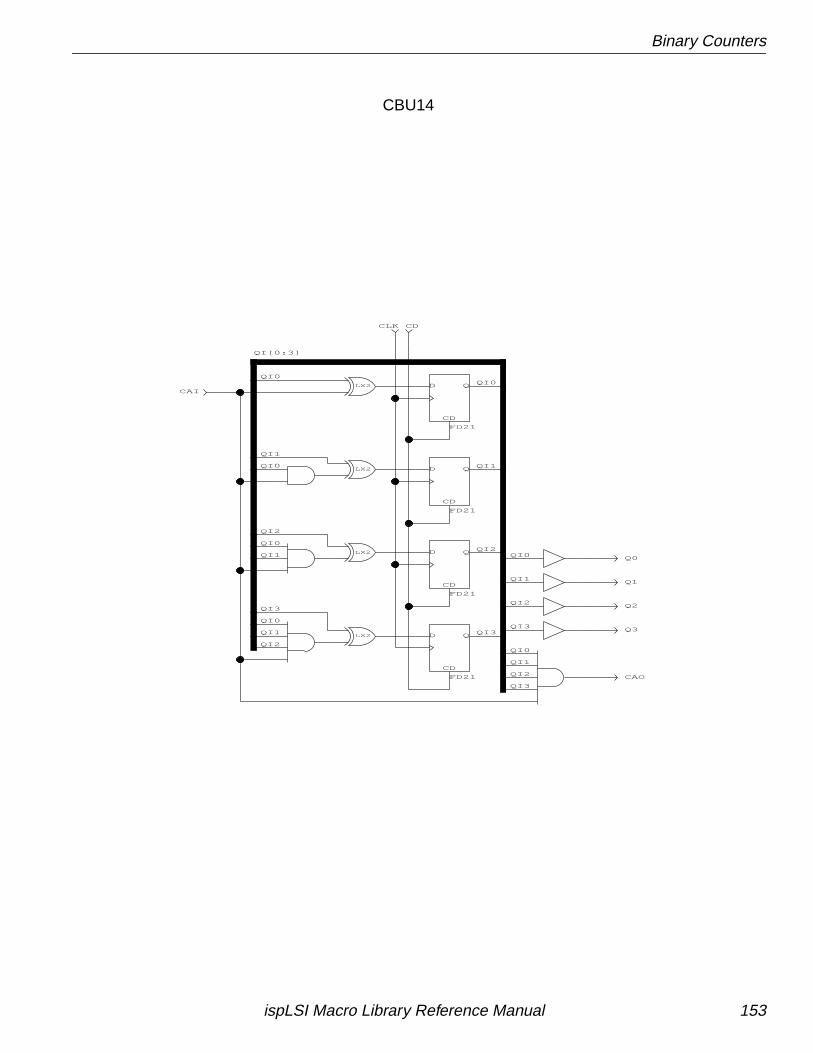
Binary Counters
CLK
CD
QD
FD21
CD
QD
FD21
CAI
CAO
CD
LX2
LX2
LX2
LX2
CD
QD
FD21
CD
QD
FD21
QI3
QI2
QI0
QI1
QI2
QI0
QI1
QI3
QI0
QI1
QI2
QI0
QI0
QI[0:3]
QI3
QI2
QI1
QI0
QI1
QI0
QI1
QI3
QI2
Q0
Q1
Q2
Q3
CBU14
ispLSI Macro Library Reference Manual 153
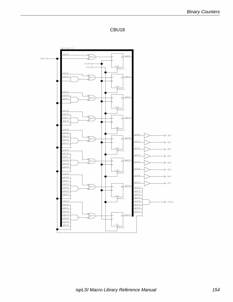
Binary Counters
Q0
Q1
Q2
Q3
Q4
Q5
Q6
Q7
QI[0:7]
QI0
QI1
QI0
QI2
QI5
QI0
QI1
QI2
QI3
QI4
QI6
QI6
QI5
QI4
QI3
QI2
QI1
QI0
QI7
QI5
QI4
QI3
QI2
QI1
QI0
QI3
QI2
QI1
QI0
QI4
QI2
QI1
QI0
QI3
QI1
QI0
QI0
QI1
QI2
QI3
QI4
QI5
QI6
QI7
QI7
QI6
QI5
QI4
QI3
QI2
QI1
QI0
QI0
QI1
QI2
QI3
QI4
QI5
QI6
QI7
CD
QD
FD21
CD
QD
FD21
CD
QD
FD21
CD
QD
FD21
CD
QD
FD21
CAI
CD
QD
FD21
CD
QD
FD21
CAO
CD
QD
FD21
CLK
CD
LX2
LX2
LX2
LX2
LX2
LX2
LX2
LX2
CBU18
ispLSI Macro Library Reference Manual 154
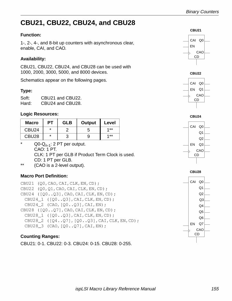
Binary Counters
CBU21, CBU22, CBU24, and CBU28
Function:
1-, 2-, 4-, and 8-bit up counters with asynchronous clear,enable, CAI, and CAO.
Availability:
CBU21, CBU22, CBU24, and CBU28 can be used with1000, 2000, 3000, 5000, and 8000 devices.
Schematics appear on the following pages.
Type:
Soft: CBU21 and CBU22.Hard: CBU24 and CBU28.
Logic Resources:
* Q0-Qn-1: 2 PT per output.CAO: 1 PT.CLK: 1 PT per GLB if Product Term Clock is used.CD: 1 PT per GLB.
** (CAO is a 2-level output).
Macro Port Definition:
CBU21 (Q0,CAO,CAI,CLK,EN,CD);CBU22 (Q0,Q1,CAO,CAI,CLK,EN,CD);CBU24 ([Q0..Q3],CAO,CAI,CLK,EN,CD);
CBU24_1 ([Q0..Q3],CAI,CLK,EN,CD);CBU24_2 (CAO,[Q0..Q3],CAI,EN);
CBU28 ([Q0..Q7],CAO,CAI,CLK,EN,CD);CBU28_1 ([Q0..Q3],CAI,CLK,EN,CD);CBU28_2 ([Q4..Q7],[Q0..Q3],CAI,CLK,EN,CD);CBU28_3 (CAO,[Q0..Q7],CAI,EN);
Counting Ranges:
CBU21: 0-1. CBU22: 0-3. CBU24: 0-15. CBU28: 0-255.
Macro PT GLB Output Level
CBU24 * 2 5 1**CBU28 * 3 9 1**
CBU21
CBU22
CBU24
CBU28
CDCAO
Q0CAI
CDCAO
Q1
Q0CAI
CDCAO
Q3
Q2
Q1
Q0CAI
Q7
Q6
Q5
Q4
Q3
Q2
Q1
Q0
CD
CAI
CAO
EN
EN
EN
EN
ispLSI Macro Library Reference Manual 155

Binary Counters
Truth Table:
The truth table is the same for all CBU2s.
* CAO = 1 after terminal count, when CAI = 1 and EN = 1.Q = output of flip-flop or latch, x = don’t care,↑ = rising clock edge.
Input Output
CD EN CAI CLK Q CAO
1 x x x 0 00 0 x x Q 00 x 0 x Q 00 1 1 ↑ count up *
ispLSI Macro Library Reference Manual 156
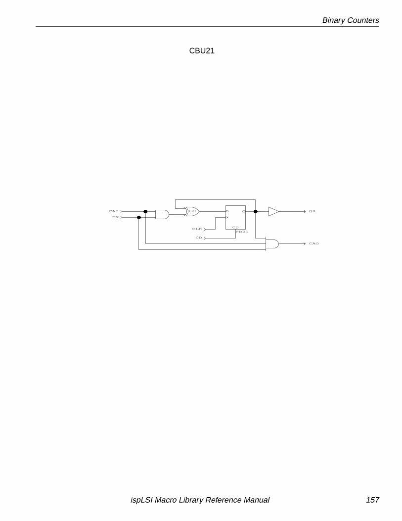
Binary Counters
Q0LX2
CLK
CD
CAO
EN
CAI
CD
QD
FD21
CBU21
ispLSI Macro Library Reference Manual 157
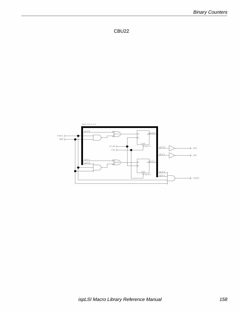
Binary Counters
QI1
QI1
QI0
QI1
QI0
QI1
QI0
QI[0:1]
QI0
QI0
CD
QD
FD21Q0
Q1
LX2
LX2
CD
CAI
EN
CD
QD
FD21
CLK
CAO
CBU22
ispLSI Macro Library Reference Manual 158
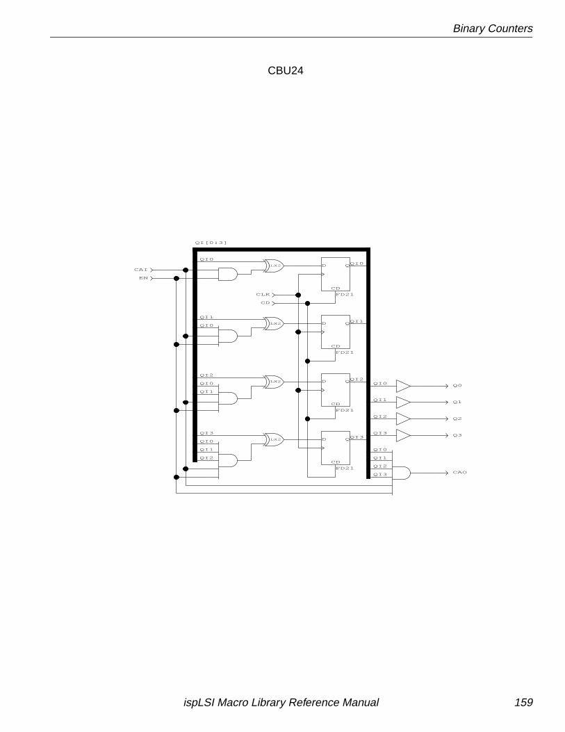
Binary Counters
QI2
QI0
QI0
QI1
QI1
QI0
QI[0:3]
QI0
QI1
QI0
QI0
QI1
QI0
QI1
QI2
QI3
QI2
QI2
QI3QI3
QI3
QI2
QI1
Q0
Q1
Q3
Q2
LX2
LX2
LX2
LX2
EN
CD
QD
FD21
CD
QD
FD21
CD
QD
FD21
CD
QD
FD21
CAI
CD
CLK
CAO
CBU24
ispLSI Macro Library Reference Manual 159
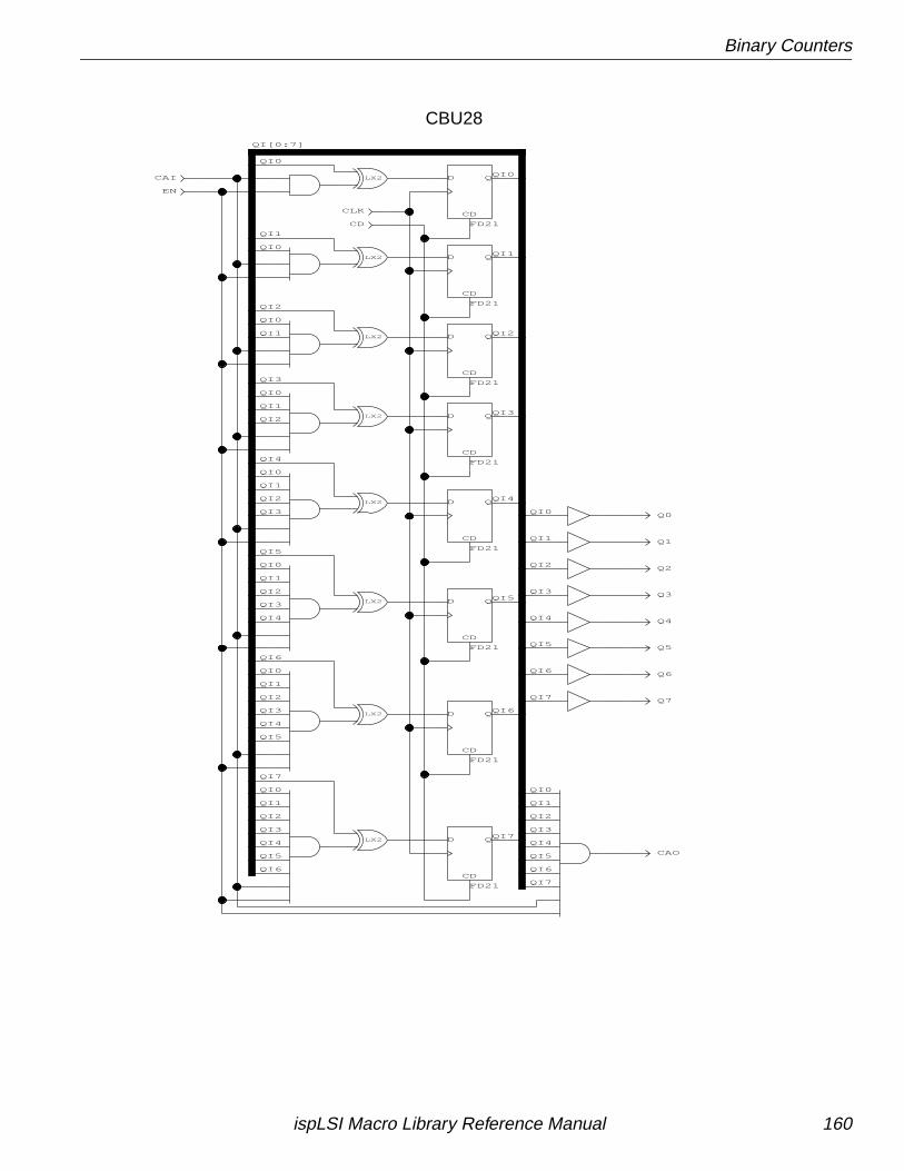
Binary Counters
Q0
Q1QI1
QI0
QI5
QI7
QI6
QI4
QI6
QI7
QI7
QI6
QI5
QI4
QI3
QI2
QI1
QI0
QI5
QI4
QI2
QI[0:7]
QI0
QI1
QI0
QI2
QI4
QI5
QI0
QI1
QI2
QI3
QI4
QI5
QI0
QI1
QI2
QI3
QI4
QI5
QI6
QI7
QI6
QI4
QI3
QI2
QI1
QI0
QI3
QI2
QI1
QI0
QI2
QI1
QI0
QI3
QI1
QI0
QI0
QI1
QI3
QI2
QI3
Q4
Q5
Q6
Q7
Q3
Q2
CD
QD
FD21
CD
QD
FD21
CLK
CAI
EN
CD
QD
FD21
CD
QD
FD21
CD
QD
FD21
CAO
CD
QD
FD21
CD
QD
FD21
CD
CD
QD
FD21
LX2
LX2
LX2
LX2
LX2
LX2
LX2
LX2
CBU28
ispLSI Macro Library Reference Manual 160
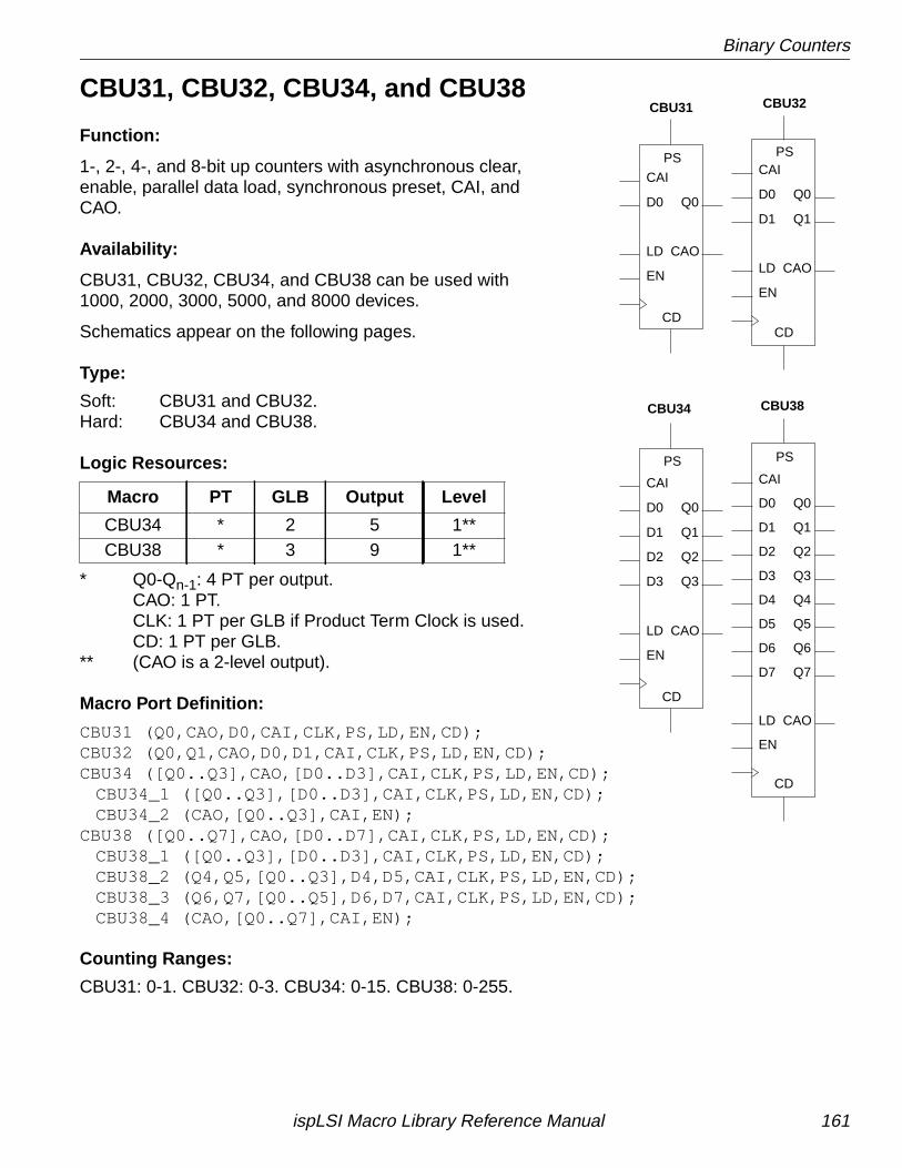
Binary Counters
CBU31, CBU32, CBU34, and CBU38
Function:
1-, 2-, 4-, and 8-bit up counters with asynchronous clear,enable, parallel data load, synchronous preset, CAI, andCAO.
Availability:
CBU31, CBU32, CBU34, and CBU38 can be used with1000, 2000, 3000, 5000, and 8000 devices.
Schematics appear on the following pages.
Type:
Soft: CBU31 and CBU32.Hard: CBU34 and CBU38.
Logic Resources:
* Q0-Qn-1: 4 PT per output.CAO: 1 PT.CLK: 1 PT per GLB if Product Term Clock is used.CD: 1 PT per GLB.
** (CAO is a 2-level output).
Macro Port Definition:
CBU31 (Q0,CAO,D0,CAI,CLK,PS,LD,EN,CD);CBU32 (Q0,Q1,CAO,D0,D1,CAI,CLK,PS,LD,EN,CD);CBU34 ([Q0..Q3],CAO,[D0..D3],CAI,CLK,PS,LD,EN,CD);
CBU34_1 ([Q0..Q3],[D0..D3],CAI,CLK,PS,LD,EN,CD);CBU34_2 (CAO,[Q0..Q3],CAI,EN);
CBU38 ([Q0..Q7],CAO,[D0..D7],CAI,CLK,PS,LD,EN,CD);CBU38_1 ([Q0..Q3],[D0..D3],CAI,CLK,PS,LD,EN,CD);CBU38_2 (Q4,Q5,[Q0..Q3],D4,D5,CAI,CLK,PS,LD,EN,CD);CBU38_3 (Q6,Q7,[Q0..Q5],D6,D7,CAI,CLK,PS,LD,EN,CD);CBU38_4 (CAO,[Q0..Q7],CAI,EN);
Counting Ranges:
CBU31: 0-1. CBU32: 0-3. CBU34: 0-15. CBU38: 0-255.
Macro PT GLB Output Level
CBU34 * 2 5 1**CBU38 * 3 9 1**
CBU31 CBU32
CBU34 CBU38
PS
Q0
CAO
EN
CAI
LD
D0
CD
D0
D1
LD
CAI
EN
Q1
CAO
Q0
PS
CD
PS
Q0
CAO
Q1
Q2
Q3
EN
CAI
LD
D3
D2
D1
D0
CD
PS
D0
D1
D2
D3
D4
D5
D6
LD
D7
CAI
EN
Q7
Q6
Q5
Q4
Q3
Q2
Q1
CAO
Q0
CD
ispLSI Macro Library Reference Manual 161
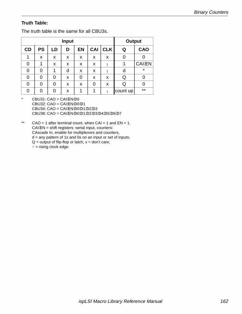
Binary Counters
Truth Table:
The truth table is the same for all CBU3s.
* CBU31: CAO = CAI⋅EN⋅D0CBU32: CAO = CAI⋅EN⋅D0⋅D1CBU34: CAO = CAI⋅EN⋅D0⋅D1⋅D2⋅D3CBU38: CAO = CAI⋅EN⋅D0⋅D1⋅D2⋅D3⋅D4⋅D5⋅D6⋅D7
** CAO = 1 after terminal count, when CAI = 1 and EN = 1.CAI⋅EN = shift registers: serial input, counters:CAscade In, enable for multiplexors and counters,d = any pattern of 1s and 0s on an input or set of inputs,Q = output of flip-flop or latch, x = don’t care,↑ = rising clock edge.
Input Output
CD PS LD D EN CAI CLK Q CAO
1 x x x x x x 0 00 1 x x x x ↑ 1 CAI⋅EN0 0 1 d x x ↑ d *0 0 0 x 0 x x Q 00 0 0 x x 0 x Q 00 0 0 x 1 1 ↑ count up **
ispLSI Macro Library Reference Manual 162
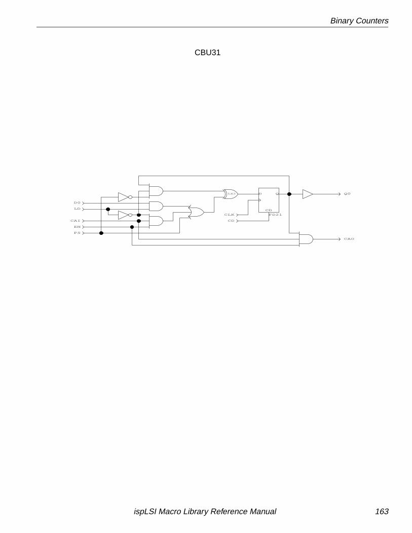
Binary Counters
Q0LX2
PS
EN
CAI
LD
D0
CAO
CLK
CD
QD
FD21
CD
CBU31
ispLSI Macro Library Reference Manual 163
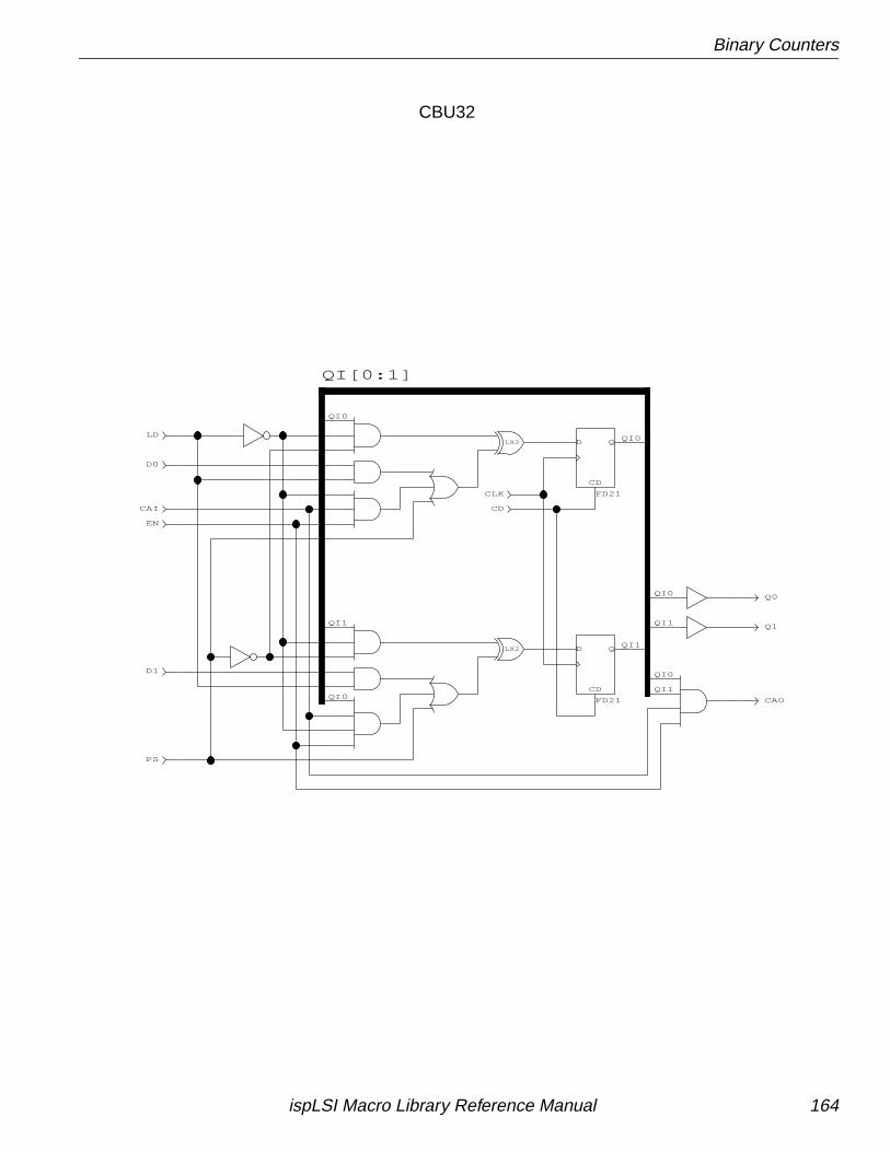
Binary Counters
CD
CLK
LX2
LX2
PS
D1
EN
CAI
D0
LD
CAO
CD
QD
FD21
CD
QD
FD21
Q1
Q0
QI1
QI[0:1]
QI0
QI1
QI0
QI0
QI1
QI0
QI1
QI0
CBU32
ispLSI Macro Library Reference Manual 164
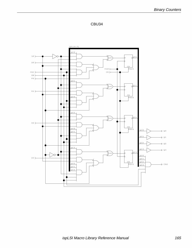
Binary Counters
Q0
QI2
QI[0:3]
QI0
QI1
QI0
QI0
QI1
QI0
QI1
QI2
QI3
QI2
QI0
QI1
QI3
QI0
QI1
QI2
QI3
QI3
QI2
QI1
QI0
Q1
Q2
Q3
CD
QD
FD21
CD
QD
FD21
CD
QD
FD21
LX2
LX2
LX2
LX2
D2
D1
D0
PS
EN
CAI
LD
CD
CD
QD
FD21
CAO
CLK
D3
CBU34
ispLSI Macro Library Reference Manual 165
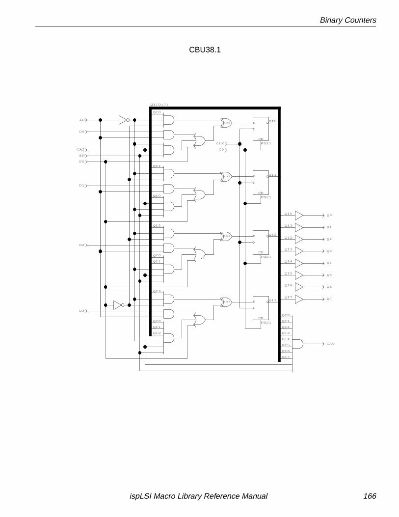
Binary Counters
Q1
Q0QI0
QI1
QI2
QI0
QI7
QI6
QI5
QI4
QI3
QI2
QI1
QI3QI7
QI6
QI5
QI4
QI3
QI2
QI1
QI0
QI[0:7]
QI2
QI3
QI2
QI1
QI0
QI1
QI0
QI0
QI1
QI0
Q2
Q3
Q4
Q5
Q6
Q7
CD
QD
FD21
CD
QD
FD21
CD
QD
FD21
LX2
LX2
LX2
LX2
D3
D2
D1
D0
LD
PS
EN
CAI
CLK
CD
CAO
CD
QD
FD21
CBU38.1
ispLSI Macro Library Reference Manual 166
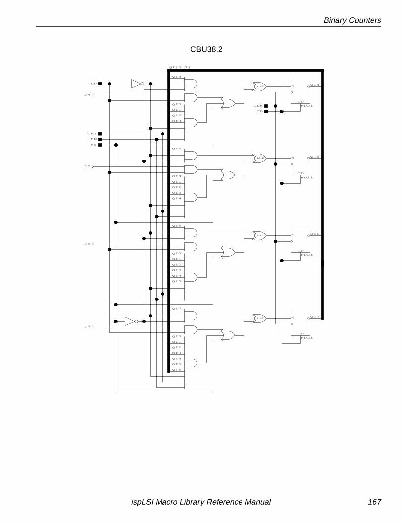
Binary Counters
QI6
QI0
QI4
QI5
QI5
QI6
QI5
QI4
QI3
QI2
QI1
QI0
QI7
QI4
QI3
QI2
QI1
QI6
QI4
QI3
QI2
QI1
QI0
QI5
QI3
QI2
QI1
QI0
QI4
QI7
QI[0:7]
CD
QD
FD21
PS
LX2
LX2
LX2
LX2
D4
D5
D6
D7
CD
QD
FD21
CD
CLK
LD
CAI
EN
CD
QD
FD21
CD
QD
FD21
CBU38.2
ispLSI Macro Library Reference Manual 167
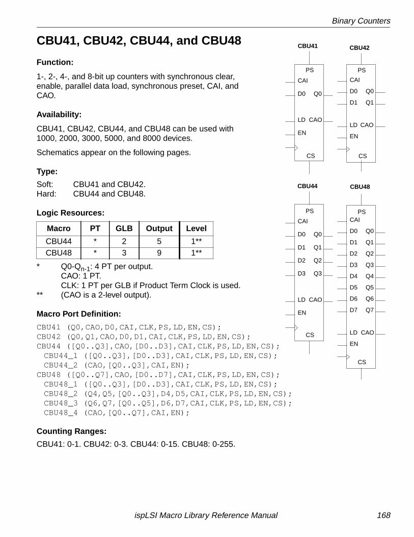
Binary Counters
CBU41, CBU42, CBU44, and CBU48
Function:
1-, 2-, 4-, and 8-bit up counters with synchronous clear,enable, parallel data load, synchronous preset, CAI, andCAO.
Availability:
CBU41, CBU42, CBU44, and CBU48 can be used with1000, 2000, 3000, 5000, and 8000 devices.
Schematics appear on the following pages.
Type:
Soft: CBU41 and CBU42.Hard: CBU44 and CBU48.
Logic Resources:
* Q0-Qn-1: 4 PT per output.CAO: 1 PT.CLK: 1 PT per GLB if Product Term Clock is used.
** (CAO is a 2-level output).
Macro Port Definition:
CBU41 (Q0,CAO,D0,CAI,CLK,PS,LD,EN,CS);CBU42 (Q0,Q1,CAO,D0,D1,CAI,CLK,PS,LD,EN,CS);CBU44 ([Q0..Q3],CAO,[D0..D3],CAI,CLK,PS,LD,EN,CS);
CBU44_1 ([Q0..Q3],[D0..D3],CAI,CLK,PS,LD,EN,CS);CBU44_2 (CAO,[Q0..Q3],CAI,EN);
CBU48 ([Q0..Q7],CAO,[D0..D7],CAI,CLK,PS,LD,EN,CS);CBU48_1 ([Q0..Q3],[D0..D3],CAI,CLK,PS,LD,EN,CS);CBU48_2 (Q4,Q5,[Q0..Q3],D4,D5,CAI,CLK,PS,LD,EN,CS);CBU48_3 (Q6,Q7,[Q0..Q5],D6,D7,CAI,CLK,PS,LD,EN,CS);CBU48_4 (CAO,[Q0..Q7],CAI,EN);
Counting Ranges:
CBU41: 0-1. CBU42: 0-3. CBU44: 0-15. CBU48: 0-255.
Macro PT GLB Output Level
CBU44 * 2 5 1**CBU48 * 3 9 1**
CBU41 CBU42
CBU44 CBU48
PS
Q0
CAO
EN
CAI
LD
D0
CS
D0
D1
LD
CAI
EN
Q1
CAO
Q0
PS
CS
PS
Q0
CAO
Q1
Q2
Q3
EN
CAI
LD
D3
D2
D1
D0
CS
PS
D0
D1
D2
D3
D4
D5
D6
LD
D7
CAI
EN
Q7
Q6
Q5
Q4
Q3
Q2
Q1
CAO
Q0
CS
ispLSI Macro Library Reference Manual 168
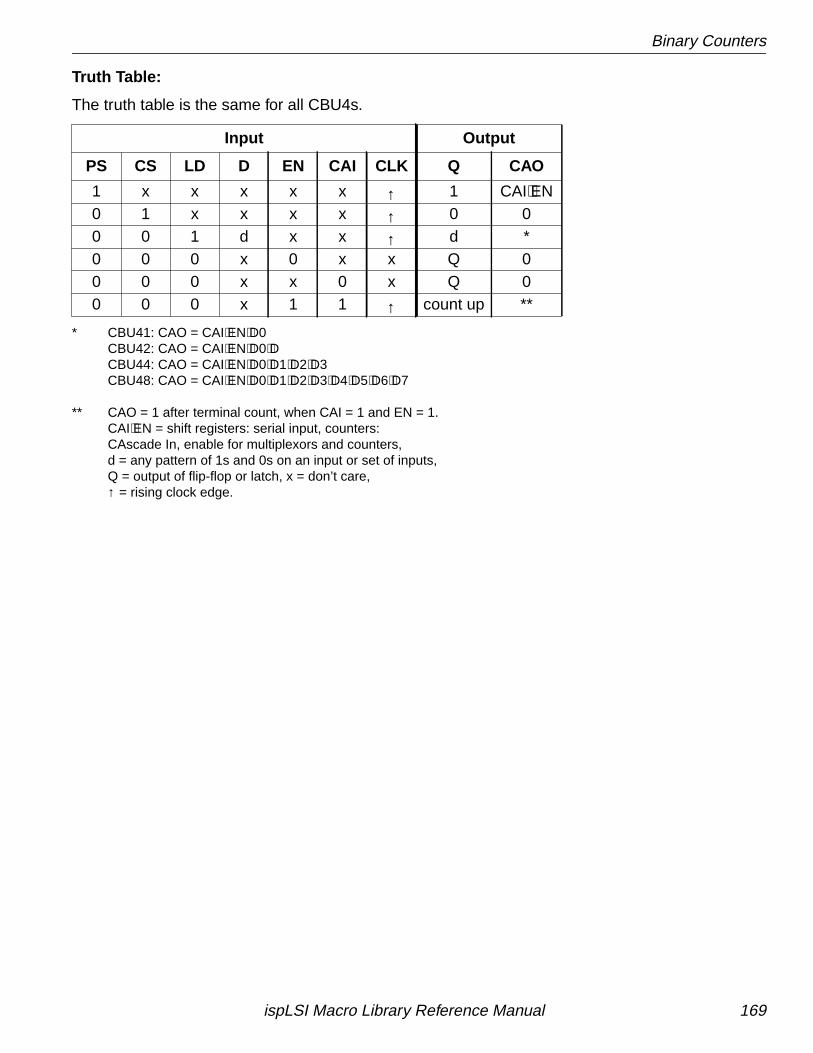
Binary Counters
Truth Table:
The truth table is the same for all CBU4s.
* CBU41: CAO = CAI⋅EN⋅D0CBU42: CAO = CAI⋅EN⋅D0⋅DCBU44: CAO = CAI⋅EN⋅D0⋅D1⋅D2⋅D3CBU48: CAO = CAI⋅EN⋅D0⋅D1⋅D2⋅D3⋅D4⋅D5⋅D6⋅D7
** CAO = 1 after terminal count, when CAI = 1 and EN = 1.CAI⋅EN = shift registers: serial input, counters:CAscade In, enable for multiplexors and counters,d = any pattern of 1s and 0s on an input or set of inputs,Q = output of flip-flop or latch, x = don’t care,↑ = rising clock edge.
Input Output
PS CS LD D EN CAI CLK Q CAO
1 x x x x x ↑ 1 CAI⋅EN0 1 x x x x ↑ 0 00 0 1 d x x ↑ d *0 0 0 x 0 x x Q 00 0 0 x x 0 x Q 00 0 0 x 1 1 ↑ count up **
ispLSI Macro Library Reference Manual 169
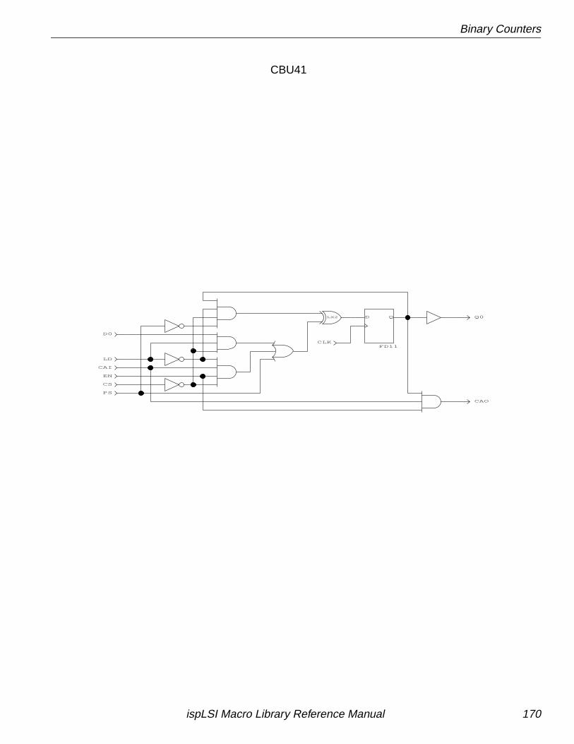
Binary Counters
Q0
PS
CLK
QD
FD11
D0
LD
CAI
EN
CS
LX2
CAO
CBU41
ispLSI Macro Library Reference Manual 170
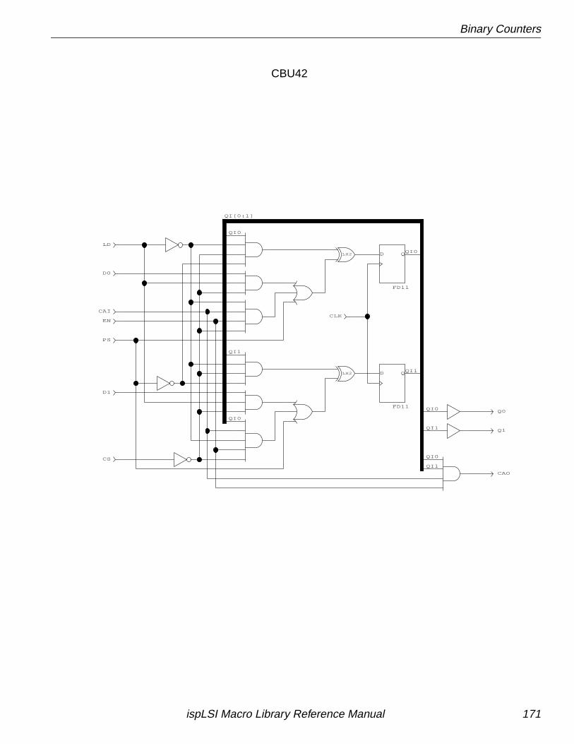
Binary Counters
Q0QI0
QI1
QI0
QI0
QI[0:1]
QI0
QI1
QI0
QI1
QI1 Q1
LX2
LX2
LD
D0
CAI
EN
PS
D1
CS
CLK
QD
FD11
QD
FD11
CAO
CBU42
ispLSI Macro Library Reference Manual 171
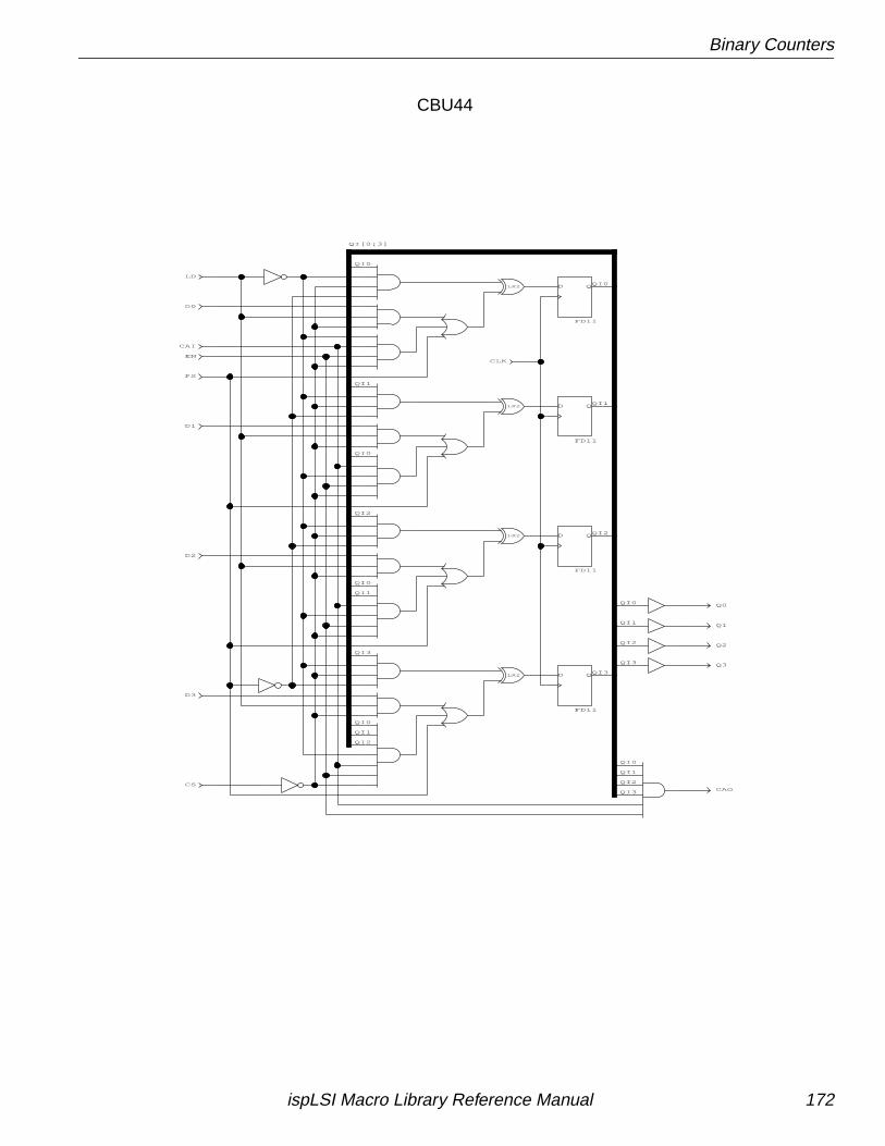
Binary Counters
Q0QI0
QI2
QI[0:3]
QI0
QI1
QI0
QI2
QI0
QI1
QI3
QI0
QI1
QI2
QI0
QI1
QI3
QI0
QI1
QI2
QI3
QI3
QI2
QI1 Q1
Q2
Q3
QD
FD11
LX2
LX2
LX2
LX2
D2
QD
FD11
LD
CAI
EN
QD
FD11
CLK
PS
D0
D1
D3
QD
FD11
CAOCS
CBU44
ispLSI Macro Library Reference Manual 172
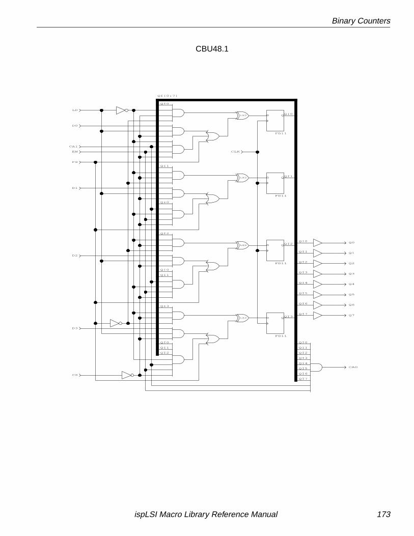
Binary Counters
Q0QI0
QI[0:7]
QI0
QI1
QI0
QI2
QI1
QI0
QI3
QI1
QI0
QI2
QI0
QI1
QI2
QI0
QI1
QI2
QI3
QI4
QI5
QI6
QI7
QI3QI7
QI6
QI5
QI4
QI3
QI2
QI1 Q1
Q2
Q4
Q3
Q7
Q6
Q5
QD
FD11
QD
FD11
LX2
LX2
LX2
LX2
CLK
LD
EN
CAI
CS
CAO
QD
FD11
QD
FD11
D3
D2
D1
PS
D0
CBU48.1
ispLSI Macro Library Reference Manual 173
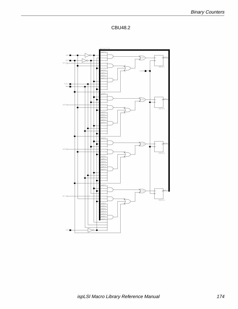
Binary Counters
QI7
QI4
QI6
QI5
QI4
QI[0:7]
QI5
QI0
QI1
QI2
QI3
QI4
QI0
QI1
QI2
QI3
QI4
QI5
QI0
QI1
QI2
QI3
QI4
QI5
QI6
QI7
QI6
QI3
QI0
QI1
QI2
QD
FD11
QD
FD11
LX2
LX2
LX2
LX2
CAI
PS
EN
LD
CLK
CS
QD
FD11
QD
FD11
D7
D6
D5
D4
CBU48.2
ispLSI Macro Library Reference Manual 174
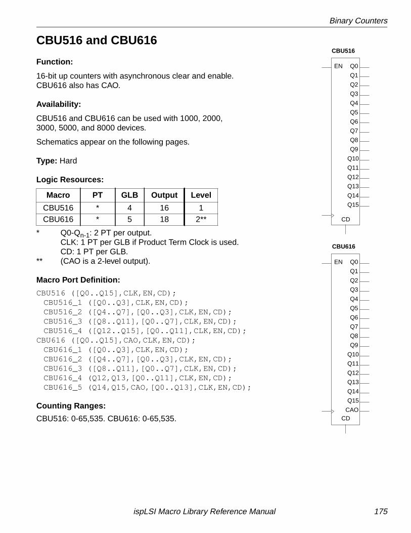
Binary Counters
CBU516 and CBU616
Function:
16-bit up counters with asynchronous clear and enable.CBU616 also has CAO.
Availability:
CBU516 and CBU616 can be used with 1000, 2000,3000, 5000, and 8000 devices.
Schematics appear on the following pages.
Type: Hard
Logic Resources:
* Q0-Qn-1: 2 PT per output.CLK: 1 PT per GLB if Product Term Clock is used.CD: 1 PT per GLB.
** (CAO is a 2-level output).
Macro Port Definition:
CBU516 ([Q0..Q15],CLK,EN,CD);CBU516_1 ([Q0..Q3],CLK,EN,CD);CBU516_2 ([Q4..Q7],[Q0..Q3],CLK,EN,CD);CBU516_3 ([Q8..Q11],[Q0..Q7],CLK,EN,CD);CBU516_4 ([Q12..Q15],[Q0..Q11],CLK,EN,CD);
CBU616 ([Q0..Q15],CAO,CLK,EN,CD);CBU616_1 ([Q0..Q3],CLK,EN,CD);CBU616_2 ([Q4..Q7],[Q0..Q3],CLK,EN,CD);CBU616_3 ([Q8..Q11],[Q0..Q7],CLK,EN,CD);CBU616_4 (Q12,Q13,[Q0..Q11],CLK,EN,CD);CBU616_5 (Q14,Q15,CAO,[Q0..Q13],CLK,EN,CD);
Counting Ranges:
CBU516: 0-65,535. CBU616: 0-65,535.
Macro PT GLB Output Level
CBU516 * 4 16 1CBU616 * 5 18 2**
CBU516
CBU616
Q0
Q1
Q2
Q3
Q4
Q5
Q6
Q7
Q8
Q10
Q11
Q12
Q13
Q14
CD
Q15
Q9
EN
EN
Q9
Q15
CAOCD
Q14
Q13
Q12
Q11
Q10
Q8
Q7
Q6
Q5
Q4
Q3
Q2
Q1
Q0
ispLSI Macro Library Reference Manual 175
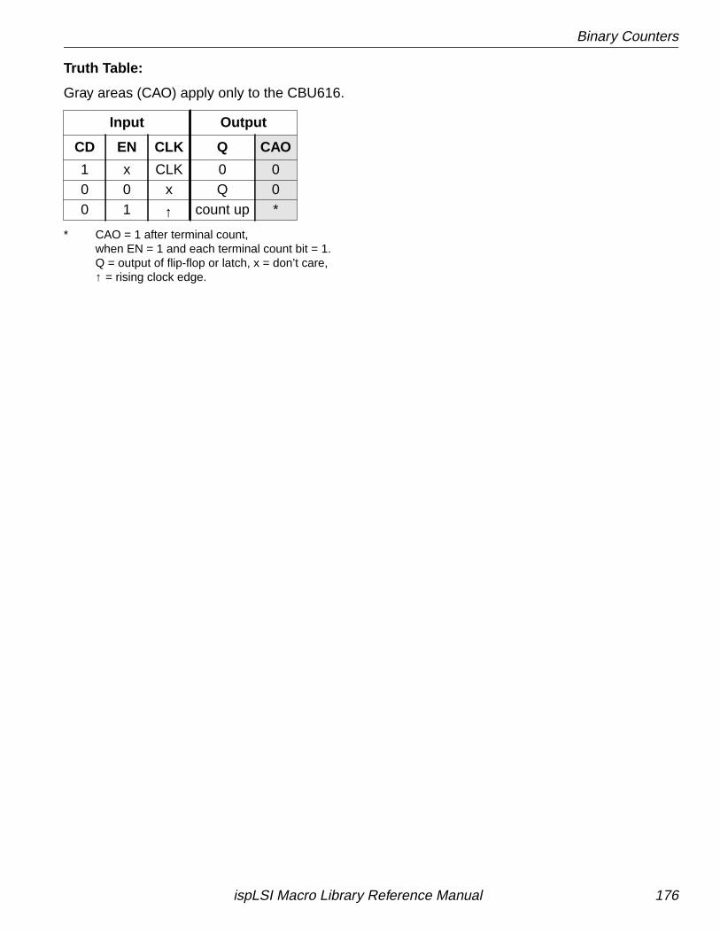
Binary Counters
Truth Table:
Gray areas (CAO) apply only to the CBU616.
* CAO = 1 after terminal count,when EN = 1 and each terminal count bit = 1.Q = output of flip-flop or latch, x = don’t care,↑ = rising clock edge.
Input Output
CD EN CLK Q CAO
1 x CLK 0 00 0 x Q 00 1 ↑ count up *
ispLSI Macro Library Reference Manual 176
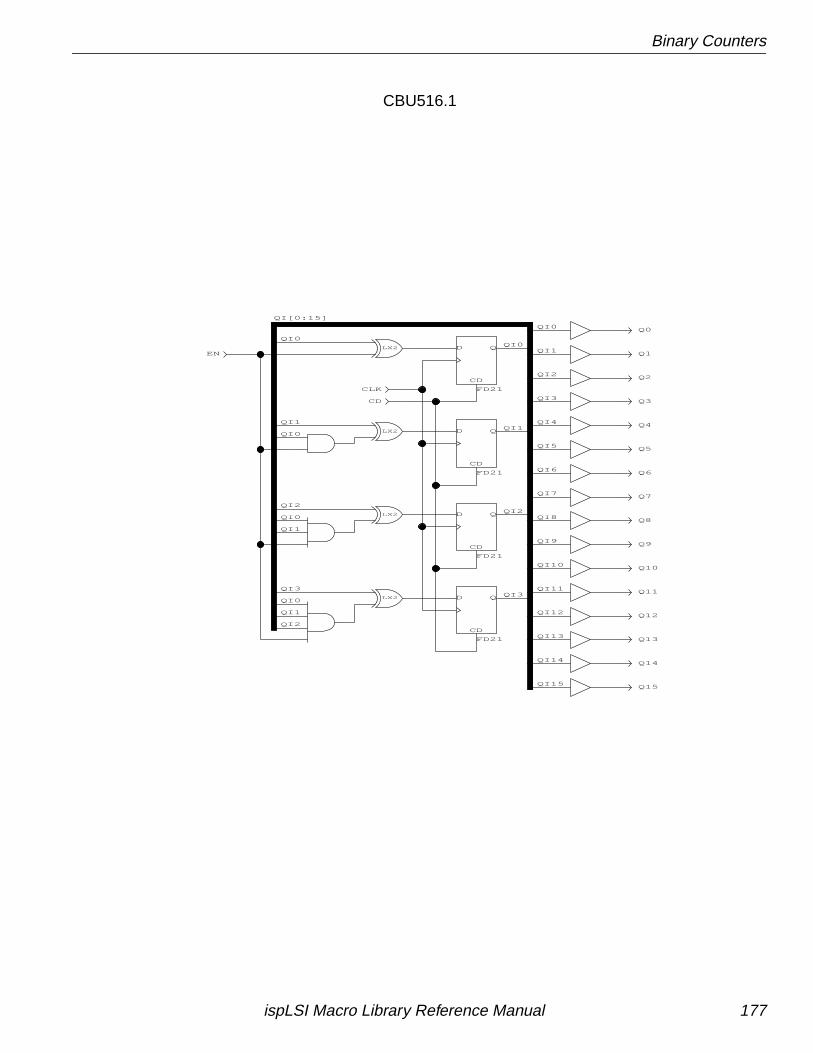
Binary Counters
QI8QI2
QI7
QI6
QI5
QI1
QI3
QI2
QI0
QI[0:15]
QI0
QI1
QI0
QI2
QI0
QI1
QI2
QI1
QI0
QI3
QI0
QI1
QI4
QI3
QI15
QI14
QI13
QI12
QI11
QI10
QI9
Q12
Q13
Q14
Q15
Q8
Q9
Q10
Q11
Q6
Q7
Q1
Q0
Q2
Q3
Q4
Q5
LX2
LX2
LX2
LX2
CD
QD
FD21
CD
QD
FD21
CD
QD
FD21
CD
CLK
CD
QD
FD21
EN
CBU516.1
ispLSI Macro Library Reference Manual 177
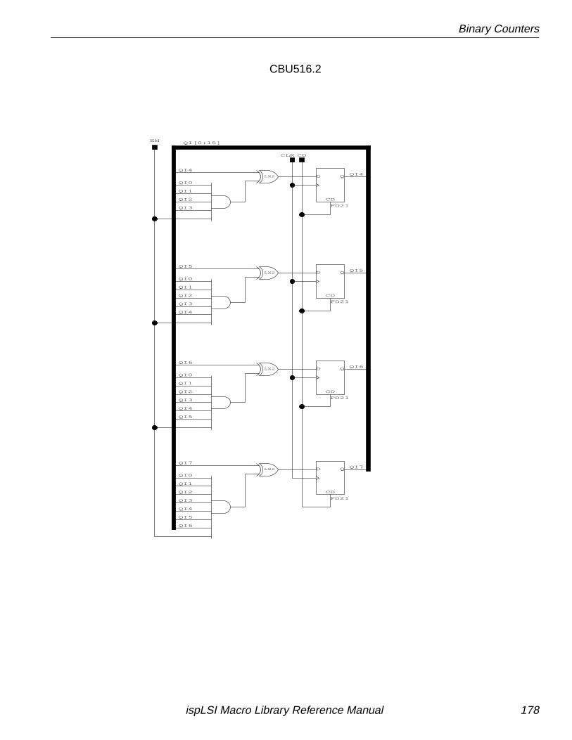
Binary Counters
CD
QD
FD21
LX2
LX2
LX2
LX2
QI0
QI2
QI1
QI3
QI4
QI5
QI6
QI0
QI1
QI2
QI3
QI4
QI5
QI0
QI1
QI2
QI3
QI4
QI0
QI1
QI2
QI3
QI[0:15]
QI4
QI5
QI7
QI4
QI5
QI6
QI7
QI6
EN
CD
QD
FD21
CD
QD
FD21
CLK CD
CD
QD
FD21
CBU516.2
ispLSI Macro Library Reference Manual 178
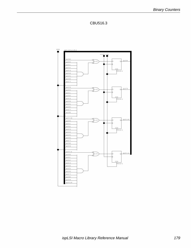
Binary Counters
LX2
LX2
LX2
LX2
CD
QD
FD21
CD
QD
FD21
CLK
CD
QD
FD21
CD
QD
FD21
CD
EN
QI11
QI10
QI9
QI8
QI11
QI10
QI9
QI[0:15]
QI8
QI7
QI6
QI5
QI4
QI3
QI2
QI1
QI0
QI8
QI7
QI6
QI5
QI4
QI2
QI3
QI1
QI0
QI9
QI8
QI7
QI6
QI5
QI4
QI3
QI2
QI1
QI0
QI10
QI9
QI8
QI7
QI6
QI5
QI4
QI2
QI3
QI1
QI0
CBU516.3
ispLSI Macro Library Reference Manual 179
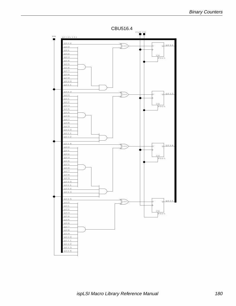
Binary Counters
LX2
LX2
LX2
LX2
CD
QD
FD21
CD
QD
FD21
CD
QD
FD21
CD
QD
FD21
EN
QI0
QI1
QI2
QI3
QI4
QI5
QI6
QI7
QI8
QI9
QI10
QI11
QI12
QI13
QI0
QI1
QI2
QI3
QI4
QI5
QI6
QI7
QI8
QI9
QI10
QI11
QI12
QI11
QI14
QI9
QI6
QI5
QI3
QI1
QI0
QI2
QI4
QI7
QI8
QI10
QI11
QI12
QI13
QI10
QI8
QI7
QI9
QI6
QI5
QI4
QI3
QI1
QI0
QI2
QI13
QI12
QI14
QI15QI15
QI14
QI13
QI12
QI[0:15]
CLK CD
CBU516.4
ispLSI Macro Library Reference Manual 180
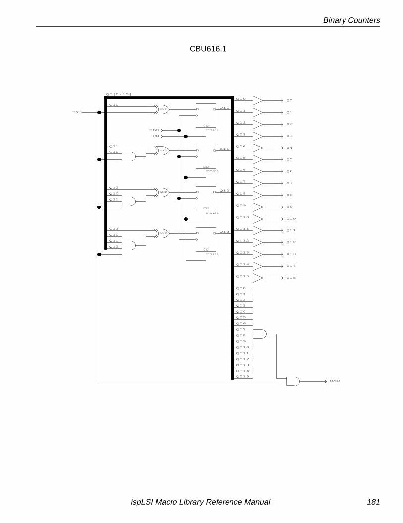
Binary Counters
Q15QI15
QI13
QI14
QI11
QI10
QI9
QI5
QI1
QI1QI0
QI[0:15]
QI0
QI1
QI0
QI2
QI0
QI1
QI0
QI1
QI2
QI3
QI0
QI2
QI3
QI4
QI6
QI7
QI2QI8
QI15
QI14
QI13
QI12
QI11
QI10
QI9
QI8
QI7
QI6
QI5
QI4
QI3
QI2
QI1
QI0
QI12
QI3
Q13
Q14
Q12
Q6
Q7
Q8
Q9
Q10
Q11
CAO
Q0
Q1
Q2
Q3
Q4
Q5
LX2
LX2
LX2
LX2
EN
CD
QD
FD21CLK
CD
CD
QD
FD21
CD
QD
FD21
CD
QD
FD21
CBU616.1
ispLSI Macro Library Reference Manual 181
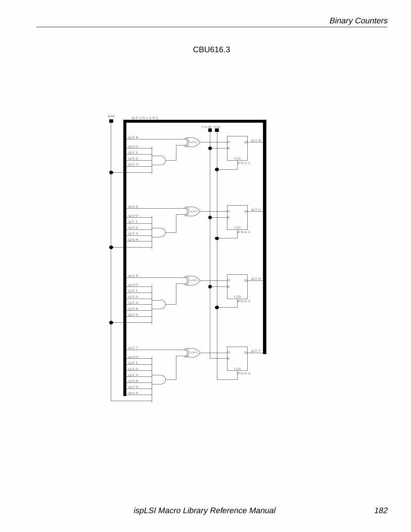
Binary Counters
CD
QD
FD21
CDCLK
CD
QD
FD21
CD
QD
FD21
EN
QI6
QI7
QI6
QI5
QI4
QI7
QI5
QI4
QI[0:15]
QI3
QI2
QI1
QI0
QI4
QI3
QI2
QI1
QI0
QI5
QI4
QI3
QI2
QI1
QI0
QI6
QI5
QI4
QI3
QI1
QI2
QI0
LX2
LX2
LX2
LX2
CD
QD
FD21
CBU616.3
ispLSI Macro Library Reference Manual 182
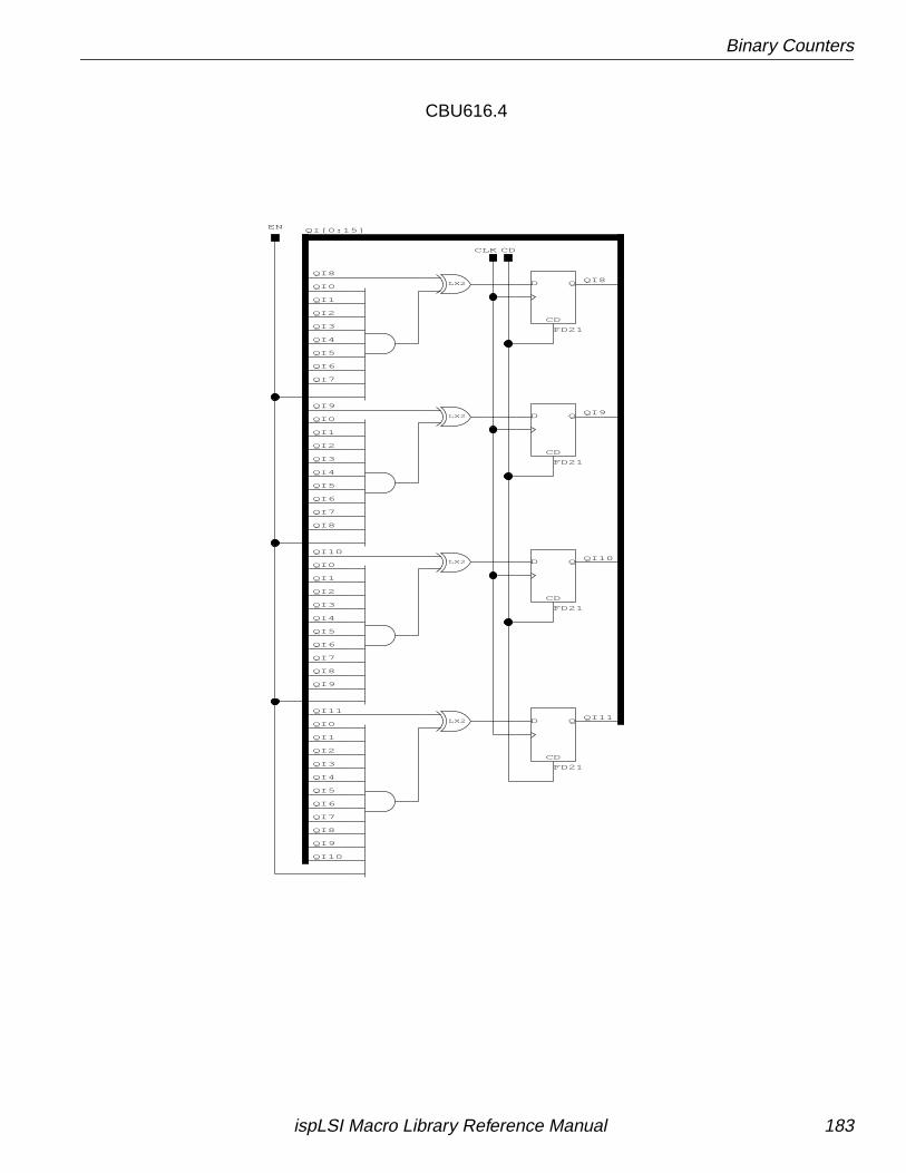
Binary Counters
QI0
QI1
QI3
QI2
QI4
QI5
QI6
QI7
QI8
QI9
QI10
QI0
QI1
QI2
QI3
QI4
QI5
QI6
QI7
QI8
QI9
QI0
QI1
QI3
QI2
QI4
QI5
QI6
QI7
QI8
QI0
QI1
QI2
QI3
QI4
QI5
QI6
QI7
QI8
QI[0:15]
QI9
QI10
QI11
QI8
QI9
QI10
QI11
EN
CD
CD
QD
FD21
CD
QD
FD21
CLK
CD
QD
FD21
CD
QD
FD21
LX2
LX2
LX2
LX2
CBU616.4
ispLSI Macro Library Reference Manual 183
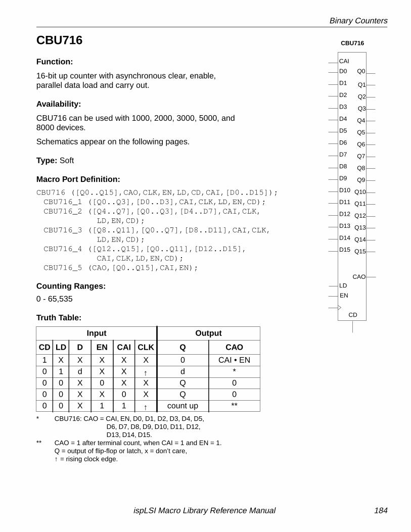
Binary Counters
CBU716
Function:
16-bit up counter with asynchronous clear, enable,parallel data load and carry out.
Availability:
CBU716 can be used with 1000, 2000, 3000, 5000, and8000 devices.
Schematics appear on the following pages.
Type: Soft
Macro Port Definition:
CBU716 ([Q0..Q15],CAO,CLK,EN,LD,CD,CAI,[D0..D15]);CBU716_1 ([Q0..Q3],[D0..D3],CAI,CLK,LD,EN,CD);CBU716_2 ([Q4..Q7],[Q0..Q3],[D4..D7],CAI,CLK,
LD,EN,CD);CBU716_3 ([Q8..Q11],[Q0..Q7],[D8..D11],CAI,CLK,
LD,EN,CD);CBU716_4 ([Q12..Q15],[Q0..Q11],[D12..D15],
CAI,CLK,LD,EN,CD);CBU716_5 (CAO,[Q0..Q15],CAI,EN);
Counting Ranges:
0 - 65,535
Truth Table:
* CBU716: CAO = CAI, EN, D0, D1, D2, D3, D4, D5,D6, D7, D8, D9, D10, D11, D12,D13, D14, D15.
** CAO = 1 after terminal count, when CAI = 1 and EN = 1.Q = output of flip-flop or latch, x = don’t care,↑ = rising clock edge.
Input Output
CD LD D EN CAI CLK Q CAO
1 X X X X X 0 CAI • EN0 1 d X X ↑ d *0 0 X 0 X X Q 00 0 X X 0 X Q 00 0 X 1 1 ↑ count up **
CBU716
Q0
Q1
Q2
Q3
Q4
Q5
Q6
Q7
Q8
Q10
Q11
Q12
Q13
Q14
CD
Q15
Q9
CAI
D0
D1
D2
D3
D4
D5
D6
D7
D8
D10
D11
D12
D13
D14
D15
D9
LD
EN
CAO
ispLSI Macro Library Reference Manual 184
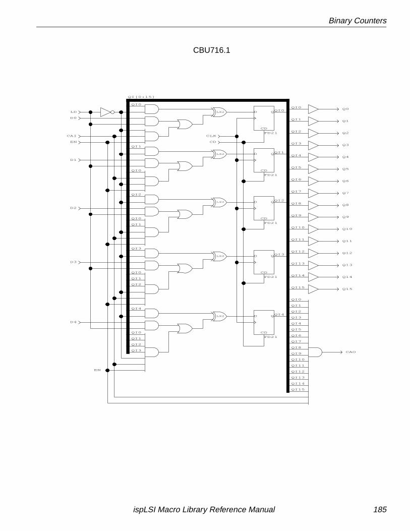
Binary Counters
EN
QI4
QI0
QI4
QI1
QI2
QI3
QI2
QI10
QI15
QI14
QI3
QI11
QI10
QI2
QI6
QI1
QI3
QI0
QI[0:15]
QI0
QI1
QI0
QI2
QI0
QI1
QI3
QI0
QI1
QI2
QI4
QI5
QI7
QI8
QI9
QI12
QI13
QI0
QI1
QI2
QI3
QI4
QI5
QI6
QI7
QI8
QI9
QI11
QI12
QI13
QI14
QI15
QI0
QI1
LX2
D4
Q4
CD
CLK
LD LX2
CD
QD
FD21
D0
CAI
EN
LX2
CD
QD
FD21
D1
LX2
CD
QD
FD21
D2
LX2
CD
QD
FD21
D3
Q3
Q2
Q1
Q0
Q5
Q6
Q7
Q8
Q9
Q10
Q11
Q12
Q13
Q14
Q15
CAO
CD
QD
FD21
CBU716.1
ispLSI Macro Library Reference Manual 185
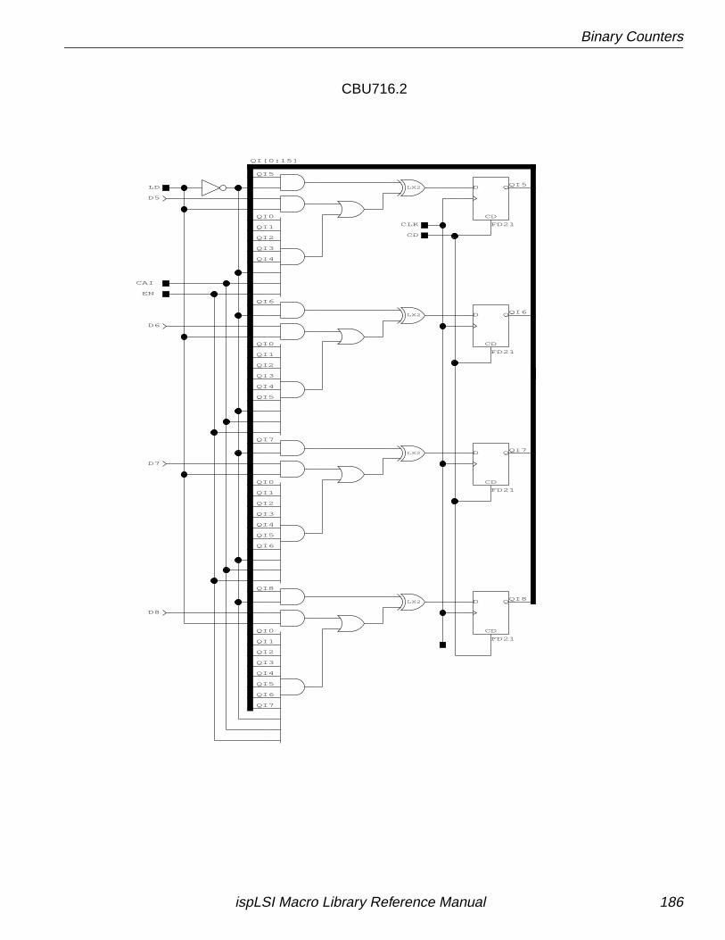
Binary Counters
LX2
D8
CD
QD
FD21
CD
QD
FD21
D5
LX2
CD
QD
FD21
D6
LX2
CD
QD
FD21
D7
LX2LD
CAI
EN
CD
CLK
QI8
QI4
QI5
QI7
QI6
QI3
QI2
QI1
QI0
QI8
QI6
QI5
QI4
QI3
QI2
QI1
QI0
QI7
QI5
QI4
QI3
QI2
QI1
QI0
QI6
QI4
QI3
QI2
QI1
QI0
QI5
QI[0:15]
QI5
QI6
QI7
CBU716.2
ispLSI Macro Library Reference Manual 186
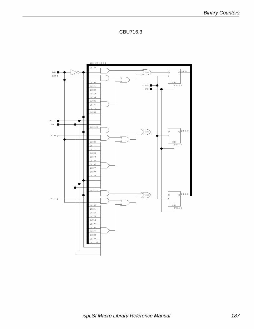
Binary Counters
CLK
CD
QD
FD21
LX2
D9
LX2
D10
D11
LX2
CD
QD
FD21
CD
QD
FD21
CD
LD
CAI
EN
QI6
QI7
QI10
QI9
QI8
QI4
QI2
QI11
QI8
QI7
QI5
QI4
QI3
QI2
QI8
QI7
QI11
QI10
QI9
QI9
QI0
QI1
QI2
QI3
QI4
QI5
QI6
QI10
QI0
QI1
QI6
QI9
QI0
QI1
QI3
QI5
QI[0:15]
CBU716.3
ispLSI Macro Library Reference Manual 187
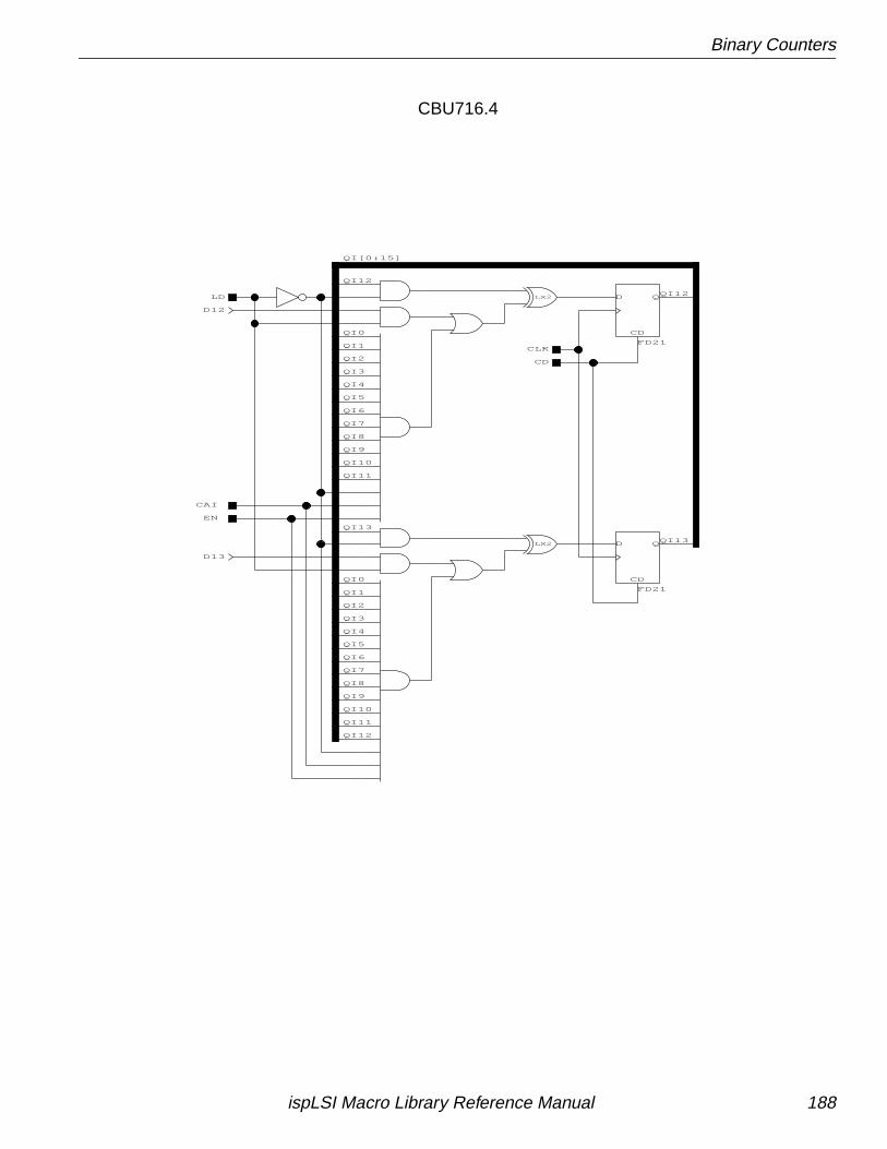
Binary Counters
QI6
QI11
QI8
QI12
QI[0:15]
QI13
QI12
QI0
QI1
QI2
QI3
QI4
QI5
QI6
QI7
QI9
QI10
QI13
QI0
QI1
QI2
QI3
QI4
QI5
QI9
QI11
QI12
QI10
QI8
QI7
LD
CAI
EN
CD
CLK
LX2
D12
D13
CD
QD
FD21
LX2
CD
QD
FD21
CBU716.4
ispLSI Macro Library Reference Manual 188
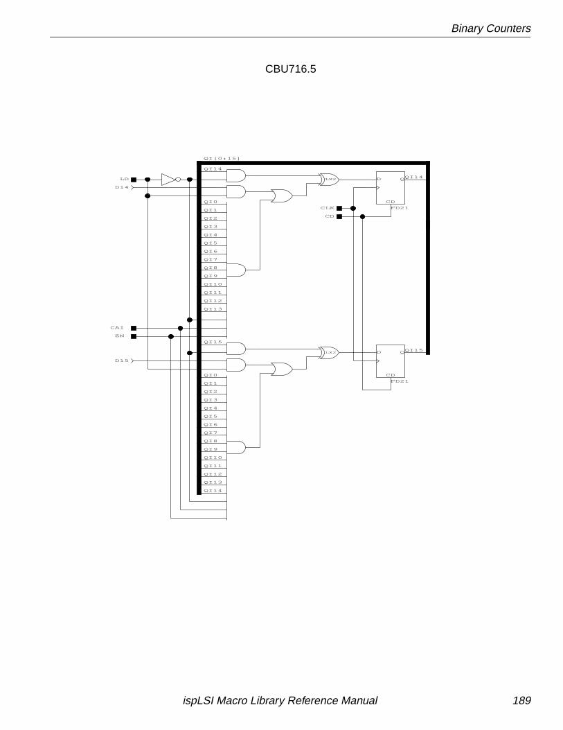
Binary Counters
QI4
QI5
QI6
QI7
QI11
QI14
QI0
QI1
QI15
QI12
QI13
QI14
QI11
QI10
QI9
QI8
QI5
QI4
QI3
QI2
QI15
QI[0:15]
QI14
QI6
QI7
QI8
QI9
QI13
QI10
QI12
QI2
QI1
QI0
QI3
EN
CAI
LX2
CD
QD
FD21
CD
LD
D14
D15
LX2
CD
QD
FD21CLK
CBU716.5
ispLSI Macro Library Reference Manual 189
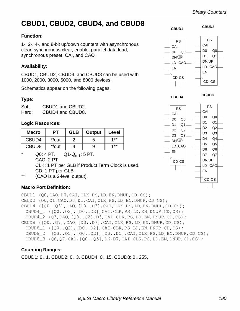
Binary Counters
CBUD1, CBUD2, CBUD4, and CBUD8
Function:
1-, 2-, 4-, and 8-bit up/down counters with asynchronousclear, synchronous clear, enable, parallel data load,synchronous preset, CAI, and CAO.
Availability:
CBUD1, CBUD2, CBUD4, and CBUD8 can be used with1000, 2000, 3000, 5000, and 8000 devices.
Schematics appear on the following pages.
Type:
Soft: CBUD1 and CBUD2.Hard: CBUD4 and CBUD8.
Logic Resources:
* Q0: 4 PT. Q1-Qn-1: 5 PT.CAO: 2 PT.CLK: 1 PT per GLB if Product Term Clock is used.CD: 1 PT per GLB.
** (CAO is a 2-level output).
Macro Port Definition:
CBUD1 (Q0,CAO,D0,CAI,CLK,PS,LD,EN,DNUP,CD,CS);CBUD2 (Q0,Q1,CAO,D0,D1,CAI,CLK,PS,LD,EN,DNUP,CD,CS);CBUD4 ([Q0..Q3],CAO,[D0..D3],CAI,CLK,PS,LD,EN,DNUP,CD,CS);
CBUD4_1 ([Q0..Q2],[D0..D2],CAI,CLK,PS,LD,EN,DNUP,CD,CS);CBUD4_2 (Q3,CAO,[Q0..Q2],D3,CAI,CLK,PS,LD,EN,DNUP,CD,CS);
CBUD8 ([Q0..Q7],CAO,[D0..D7],CAI,CLK,PS,LD,EN,DNUP,CD,CS);CBUD8_1 ([Q0..Q2],[D0..D2],CAI,CLK,PS,LD,EN,DNUP,CD,CS);CBUD8_2 [Q3..Q5],[Q0..Q2],[D3..D5],CAI,CLK,PS,LD,EN,DNUP,CD,CS);CBUD8_3 (Q6,Q7,CAO,[Q0..Q5],D6,D7,CAI,CLK,PS,LD,EN,DNUP,CD,CS);
Counting Ranges:
CBUD1: 0↔1. CBUD2: 0↔3. CBUD4: 0↔15. CBUD8: 0↔255.
Macro PT GLB Output Level
CBUD4 */out 2 5 1**CBUD8 */out 4 9 1**
CBUD1 CBUD2
CBUD4 CBUD8
DN/UP
CSCD
D0
LD
CAI
EN
CAO
Q0
PS
DN/UP
PS
Q0
CAO
Q1
EN
CAI
LD
D1
D0
CD CS
DN/UP
PS
Q0
CAO
Q1
Q2
Q3
EN
CAI
LD
D3
D2
D1
D0
CD CS DN/UP
PS
CSCD
D0
D1
D2
D3
D4
D5
D6
LD
D7
CAI
EN
Q7
Q6
Q5
Q4
Q3
Q2
Q1
CAO
Q0
ispLSI Macro Library Reference Manual 190
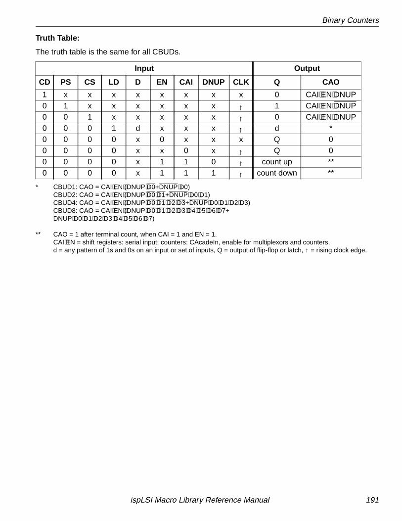
Binary Counters
Truth Table:
The truth table is the same for all CBUDs.
* CBUD1: CAO = CAI⋅EN⋅(DNUP⋅D0+DNUP⋅D0)CBUD2: CAO = CAI⋅EN⋅(DNUP⋅D0⋅D1+DNUP⋅D0⋅D1)CBUD4: CAO = CAI⋅EN⋅(DNUP⋅D0⋅D1⋅D2⋅D3+DNUP⋅D0⋅D1⋅D2⋅D3)CBUD8: CAO = CAI⋅EN⋅(DNUP⋅D0⋅D1⋅D2⋅D3⋅D4⋅D5⋅D6⋅D7+DNUP⋅D0⋅D1⋅D2⋅D3⋅D4⋅D5⋅D6⋅D7)
** CAO = 1 after terminal count, when CAI = 1 and EN = 1.CAI⋅EN = shift registers: serial input; counters: CAcadeIn, enable for multiplexors and counters,d = any pattern of 1s and 0s on an input or set of inputs, Q = output of flip-flop or latch, ↑ = rising clock edge.
Input Output
CD PS CS LD D EN CAI DNUP CLK Q CAO
1 x x x x x x x x 0 CAI⋅EN⋅DNUP0 1 x x x x x x ↑ 1 CAI⋅EN⋅DNUP0 0 1 x x x x x ↑ 0 CAI⋅EN⋅DNUP0 0 0 1 d x x x ↑ d *0 0 0 0 x 0 x x x Q 00 0 0 0 x x 0 x ↑ Q 00 0 0 0 x 1 1 0 ↑ count up **0 0 0 0 x 1 1 1 ↑ count down **
ispLSI Macro Library Reference Manual 191
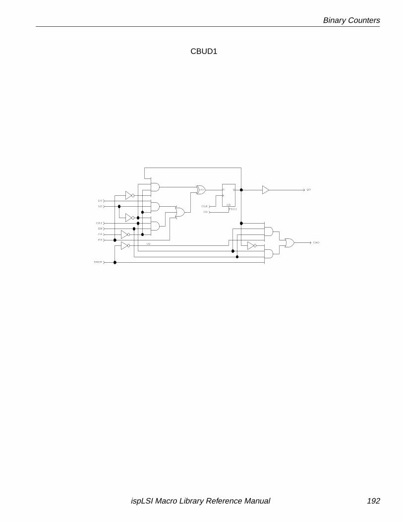
Binary Counters
Q0LX2
CD
QD
FD21CLK
CD
CAOUP
CS
EN
CAI
D0
LD
PS
DNUP
CBUD1
ispLSI Macro Library Reference Manual 192
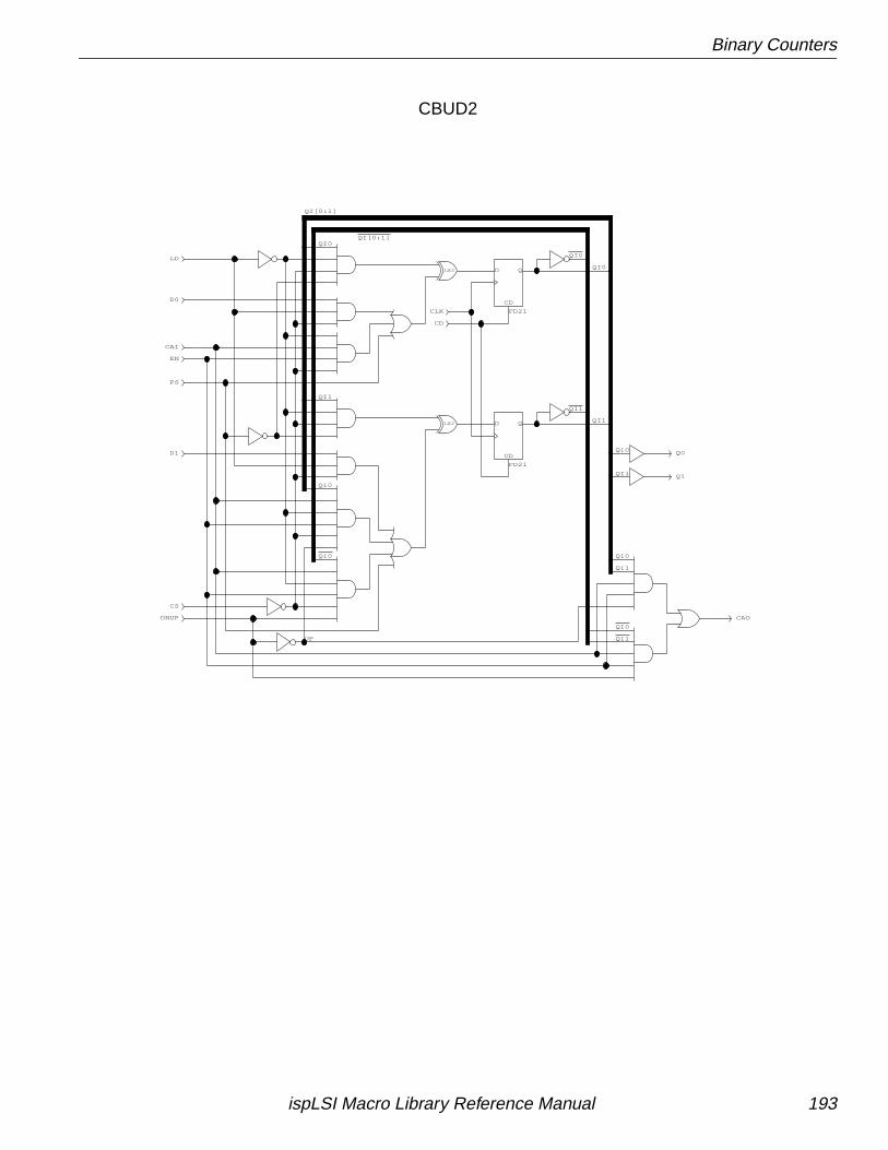
Binary Counters
QI0
QI0
QI1
QI0
QI[0:1]
QI0
QI1
QI1
QI0
QI1
QI1
QI0
QI[0:1]
QI0
QI0
QI1
Q0
Q1
CAO
LD
D0
PS
CAI
D1
CS
CLK
CD
QD
FD21
CD
QD
FD21
CD
DNUP
EN
UP
LX2
LX2
CBUD2
ispLSI Macro Library Reference Manual 193
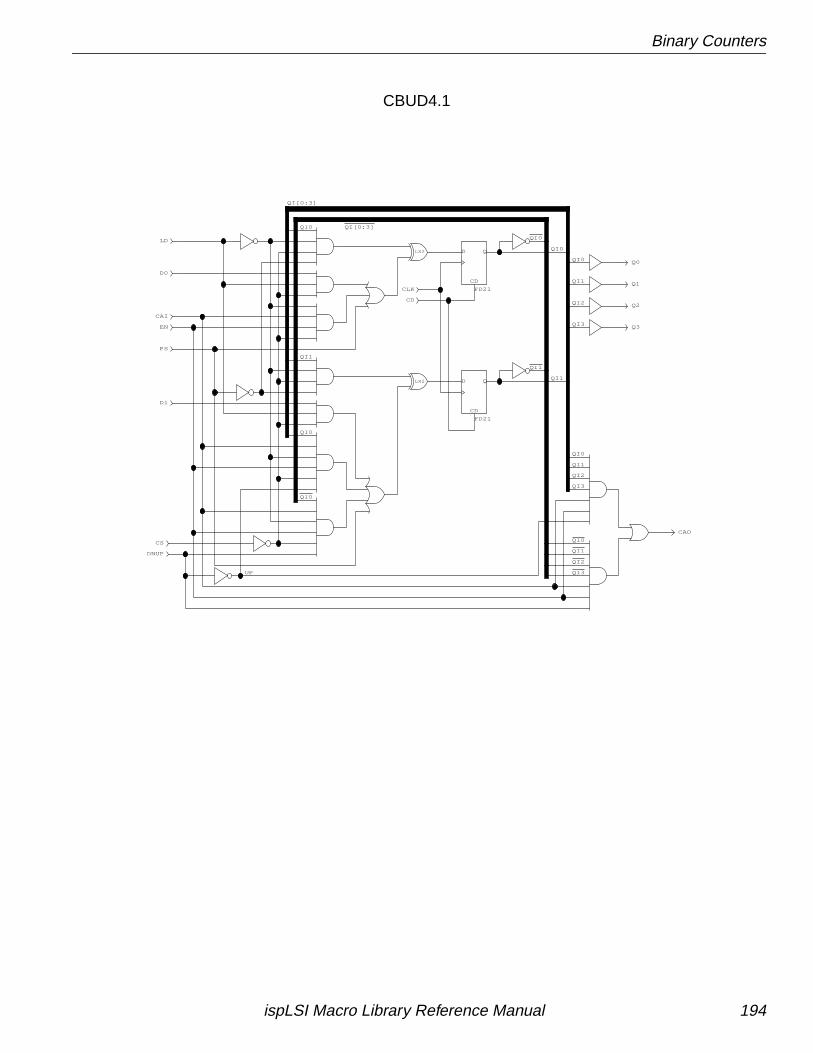
Binary Counters
Q3
Q2
Q1
Q0
QI1
QI2
QI3
QI0
QI1
QI0
QI1
QI0
QI[0:3]
QI0
QI3
QI2
QI1
QI0
UP
CAO
QI[0:3]
QI0
QI0
QI1
QI0
QI1
QI2
QI3
LX2
LX2
DNUP
CS
CD
CD
QD
FD21
CD
QD
FD21
LD
D0
D1
PS
CAI
EN
CLK
CBUD4.1
ispLSI Macro Library Reference Manual 194
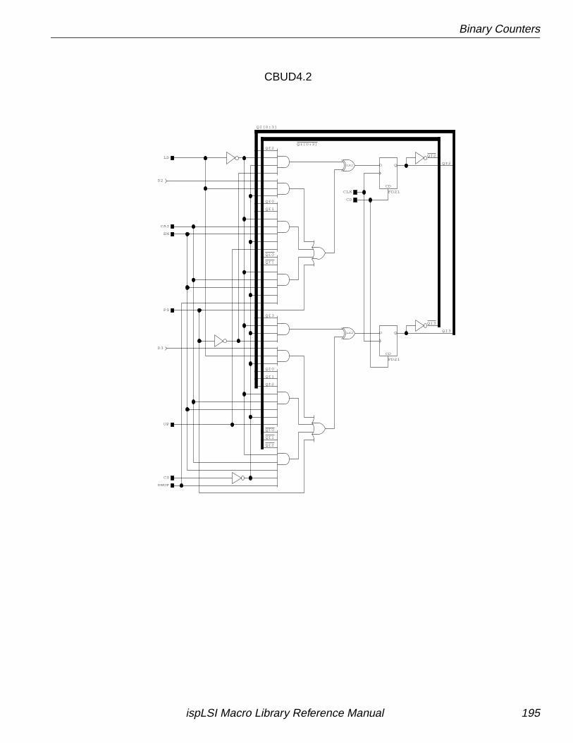
Binary Counters
QI[0:3]
QI2
QI2
QI1
QI3
QI0
QI1
QI2
QI0
QI3
LD
CD
CLK
CS
QI[0:3]
QI2
QI3
QI2
QI0
QI1
QI0
QI1
D3
D2
CD
QD
FD21
CD
QD
FD21
LX2
LX2
EN
CAI
PS
DNUP
UP
CBUD4.2
ispLSI Macro Library Reference Manual 195
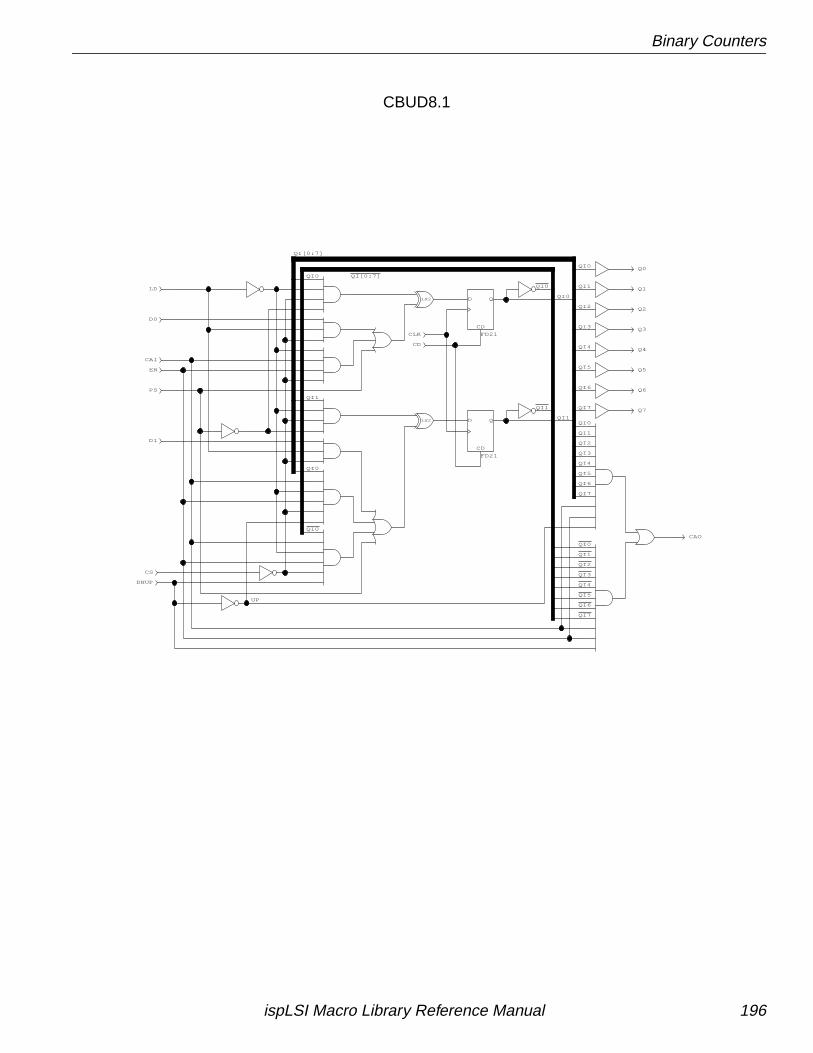
Binary Counters
QI1
QI0
QI[0:7]
QI0
QI0
QI1
QI2
QI3
QI4
QI5
QI6
QI7
Q6
Q7
Q0
Q1
Q2
Q3
Q4
Q5
QI0
QI1
QI0
QI2
QI3
QI5
QI6
QI7
QI4
QI5
QI6
QI7
QI3
QI2
QI1
QI0QI1
QI4
QI[0:7]
QI0
QI1
QI0
LX2
LX2
DNUP
CS
CAO
CD
CD
QD
FD21
CD
QD
FD21
LD
D0
D1
PS
CAI
EN
CLK
UP
CBUD8.1
ispLSI Macro Library Reference Manual 196
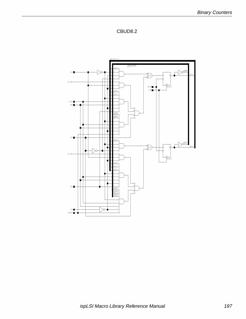
Binary Counters
QI[0:7]
QI2
QI2
QI1
QI3
QI0
QI1
QI2
QI0
QI3
DNUP
LX2
LX2
CD
CLK
CS
D3
D2
CD
QD
FD21
CD
QD
FD21
EN
CAI
PS
LD
QI[0:7]
QI2
QI3
QI2
QI0
QI1
QI0
QI1
UP
CBUD8.2
ispLSI Macro Library Reference Manual 197
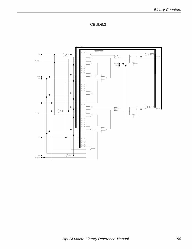
Binary Counters
DNUP
CS
UP
D5
PS
EN
CAI
D4
LD
LX2
LX2
CLK
CD
QI[0:7]
QI5
QI4
QI4
QI4
QI3
QI2
QI1
QI0
QI5
QI3
QI2
QI1
QI0
CD
QD
FD21
CD
QD
FD21
QI[0:7]
QI5
QI4
QI4
QI3
QI1
QI0
QI3
QI2
QI1
QI0
QI2
CBUD8.3
ispLSI Macro Library Reference Manual 198
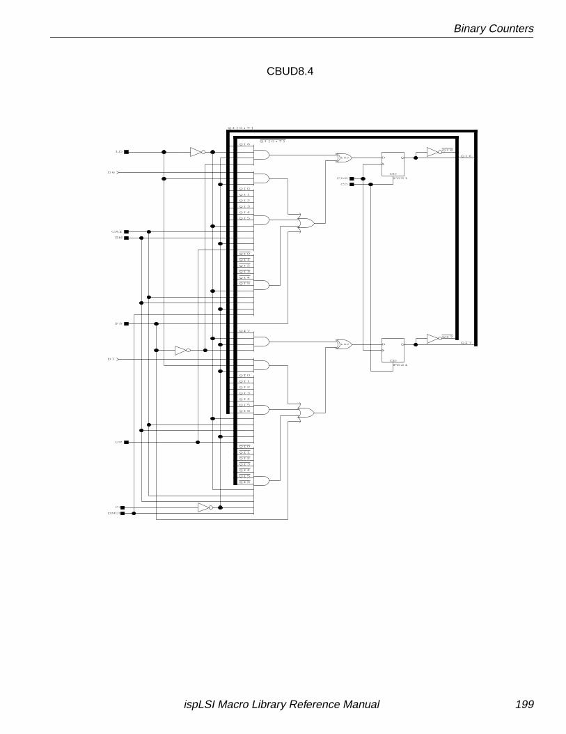
Binary Counters
QI7
QI6
QI0
QI1
QI2
QI3
QI4
QI5
QI7
QI0
QI1
QI2
QI3
QI4
QI5
QI6
QI6
QI[0:7]
LD
EN
CAI
PS
DNUP
UP
QI7
QI2
QI3
QI5
QI0
QI1
QI2
QI3
QI5
QI6
QI4
QI4
QI0
QI1
QI6
QI[0:7]
CD
QD
FD21
CD
QD
FD21
CD
CLK
LX2
LX2
CS
D7
D6
CBUD8.4
ispLSI Macro Library Reference Manual 199
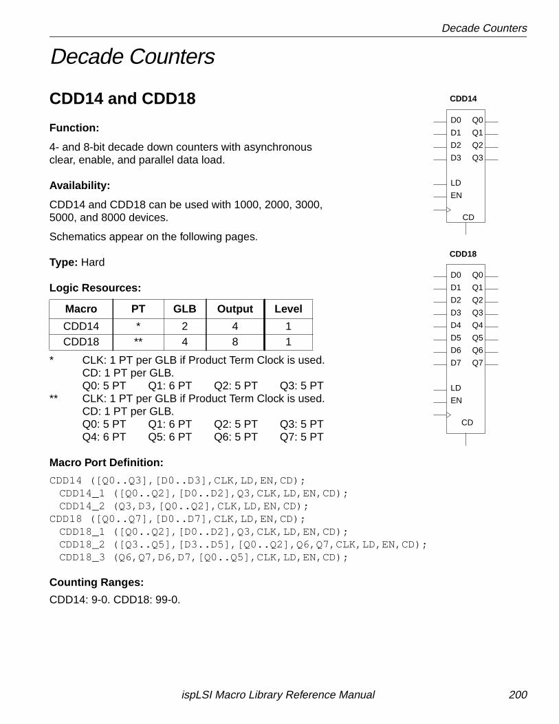
Decade Counters
Decade Counters
CDD14 and CDD18
Function:
4- and 8-bit decade down counters with asynchronousclear, enable, and parallel data load.
Availability:
CDD14 and CDD18 can be used with 1000, 2000, 3000,5000, and 8000 devices.
Schematics appear on the following pages.
Type: Hard
Logic Resources:
* CLK: 1 PT per GLB if Product Term Clock is used.CD: 1 PT per GLB.Q0: 5 PT Q1: 6 PT Q2: 5 PT Q3: 5 PT
** CLK: 1 PT per GLB if Product Term Clock is used.CD: 1 PT per GLB.Q0: 5 PT Q1: 6 PT Q2: 5 PT Q3: 5 PTQ4: 6 PT Q5: 6 PT Q6: 5 PT Q7: 5 PT
Macro Port Definition:
CDD14 ([Q0..Q3],[D0..D3],CLK,LD,EN,CD);CDD14_1 ([Q0..Q2],[D0..D2],Q3,CLK,LD,EN,CD);CDD14_2 (Q3,D3,[Q0..Q2],CLK,LD,EN,CD);
CDD18 ([Q0..Q7],[D0..D7],CLK,LD,EN,CD);CDD18_1 ([Q0..Q2],[D0..D2],Q3,CLK,LD,EN,CD);CDD18_2 ([Q3..Q5],[D3..D5],[Q0..Q2],Q6,Q7,CLK,LD,EN,CD);CDD18_3 (Q6,Q7,D6,D7,[Q0..Q5],CLK,LD,EN,CD);
Counting Ranges:
CDD14: 9-0. CDD18: 99-0.
Macro PT GLB Output Level
CDD14 * 2 4 1CDD18 ** 4 8 1
CDD14
CDD18
LD
EN
D3 Q3
D2 Q2
D1 Q1
D0 Q0
CD
Q7D7
LD
EN
D6 Q6
D5 Q5
D4 Q4
D3 Q3
D2 Q2
D1 Q1
D0 Q0
CD
ispLSI Macro Library Reference Manual 200
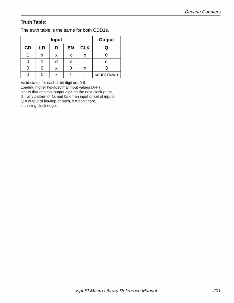
Decade Counters
Truth Table:
The truth table is the same for both CDD1s.
Valid states for each 4-bit digit are 0-9.Loading higher hexadecimal input values (A-F)clears that decimal output digit on the next clock pulse.d = any pattern of 1s and 0s on an input or set of inputs,Q = output of flip-flop or latch, x = don’t care,↑ = rising clock edge.
Input Output
CD LD D EN CLK Q
1 x x x x 00 1 d x ↑ d0 0 x 0 x Q0 0 x 1 ↑ count down
ispLSI Macro Library Reference Manual 201
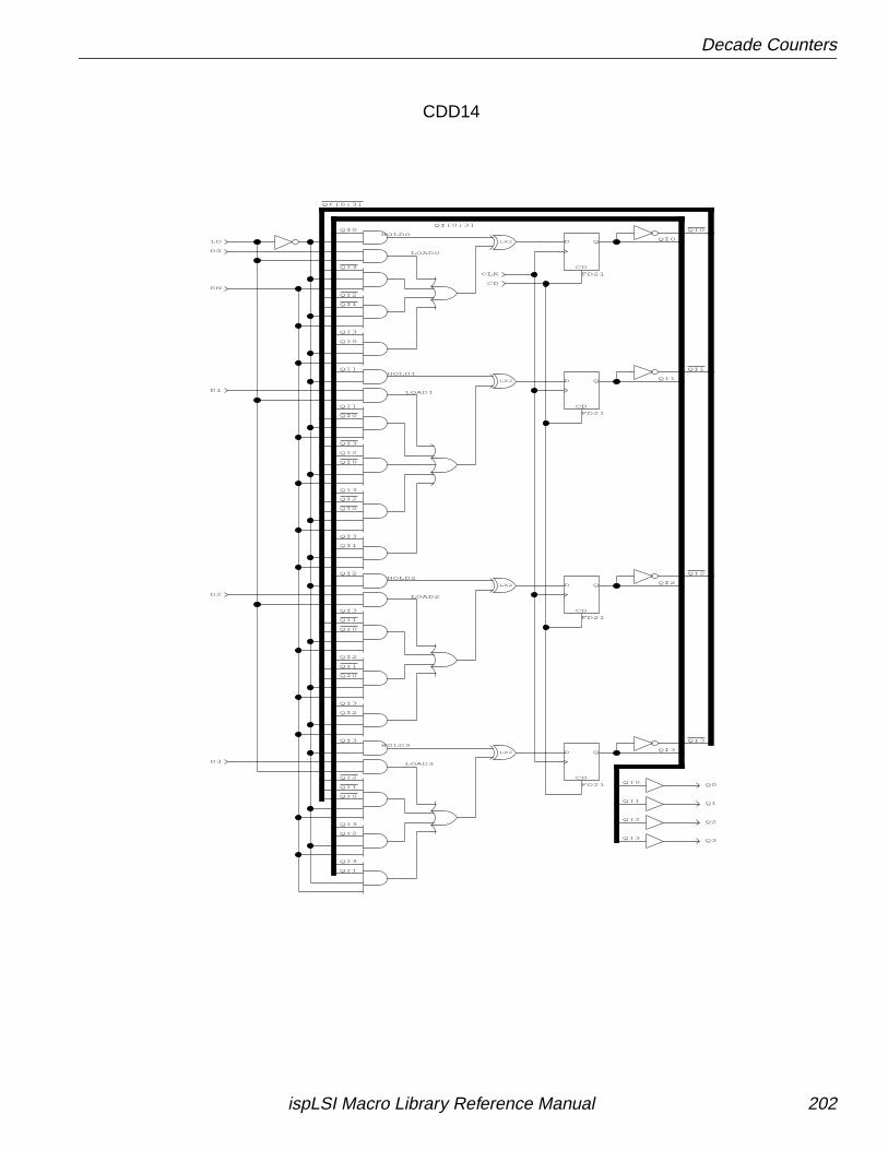
Decade Counters
QI3
QI2
QI1
QI0
QI3
QI1
QI0
QI3
QI0
QI1
QI3
QI2
QI3
QI2
QI1
QI3
QI2
QI3
QI3
QI2
QI1
QI3
QI3
QI2
QI1
QI0QI[0:3]
QI2
CD
QD
FD21
Q3
Q2
Q1
Q0
QI[0:3]
QI1
QI0
QI0
QI3
QI0
QI2
QI0
QI2
QI1
QI3
QI1
QI0
QI1
QI0
QI2
QI2
QI1
QI3
QI0
LX2
LX2
LX2
LX2
CLK
D0
LD
LOAD3
CD
QD
FD21
LOAD1
LOAD0
CD
QD
FD21
HOLD0
HOLD2
HOLD3
HOLD1
CD
QD
FD21
LOAD2
EN
D1
D2
D3
CD
CDD14
ispLSI Macro Library Reference Manual 202
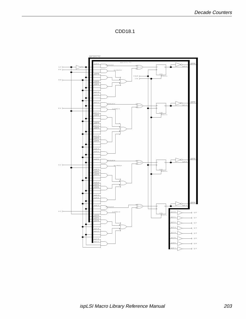
Decade Counters
HOLD3
Q7
Q6
Q5
Q4
Q3
Q2
Q1
Q0
QI2
QI3
QI4
QI5
QI6
QI3
QI1
QI0
QI3
QI0
QI1
QI3
QI2
QI3
QI2
QI1
QI3
QI2
QI3
QI3
QI2
QI1
QI3
QI3
QI2
QI1
QI0QI[0:7]
QI2
QI1
QI0
QI7
QI0
QI3
QI1
QI2
QI2
QI0
QI1
QI0
QI1
QI3
QI1
QI2
QI0
QI2
QI0
QI3
QI0
QI0
QI1
QI[0:7]
LX2
LX2
LX2
LX2
CD
D3
D2
D1
EN
LOAD2
CD
QD
FD21
HOLD1
HOLD2
HOLD0
CD
QD
FD21
LOAD0
LOAD1
CD
QD
FD21
CD
QD
FD21
LOAD3
LD
D0
CLK
CDD18.1
ispLSI Macro Library Reference Manual 203
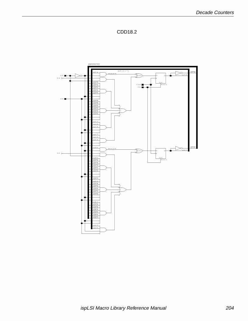
Decade Counters
QI[0:7]
QI5
QI6
QI2
QI2
QI3
QI2
QI6
QI5
QI3
QI1
QI0
QI4
QI1
QI0
QI7
QI4
QI3
QI1
QI0
QI0
QI1
QI2
QI3
QI4
QI7
QI3
QI2
QI1
QI0
QI4
LX2
LX2
CLK
CD
EN
LD
QI[0:7]
QI7
QI4
QI7
QI6
QI4
QI7
QI5
QI4
QI5
QI7
QI5
QI5
QI6
QI4
QI5
CD
QD
FD21
HOLD4
HOLD5
CD
QD
FD21
D4
D5
CDD18.2
ispLSI Macro Library Reference Manual 204
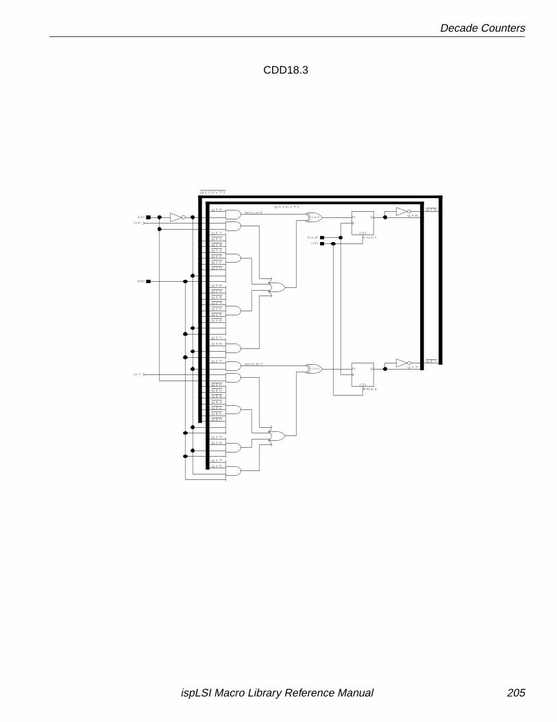
Decade Counters
QI[0:7]
QI6
QI6
QI7
QI6
QI7
QI7
QI6
QI7
QI7
QI6
QI7
QI5
LX2
LX2
CLK
CD
LD
QI[0:7]
QI5
QI4
QI3
QI1
QI0
QI2
QI1
QI3
QI2
QI0
QI6
QI7
QI4
QI5
QI5
QI4
QI3
QI2
QI1
QI0
QI6
CD
QD
FD21
CD
QD
FD21
HOLD6
HOLD7
D6
D7
EN
CDD18.3
ispLSI Macro Library Reference Manual 205
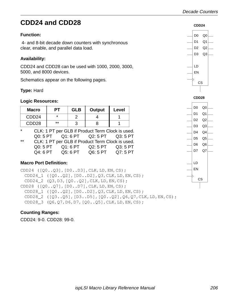
Decade Counters
CDD24 and CDD28
Function:
4- and 8-bit decade down counters with synchronousclear, enable, and parallel data load.
Availability:
CDD24 and CDD28 can be used with 1000, 2000, 3000,5000, and 8000 devices.
Schematics appear on the following pages.
Type: Hard
Logic Resources:
* CLK: 1 PT per GLB if Product Term Clock is used.Q0: 5 PT Q1: 6 PT Q2: 5 PT Q3: 5 PT
** CLK: 1 PT per GLB if Product Term Clock is used.Q0: 5 PT Q1: 6 PT Q2: 5 PT Q3: 5 PTQ4: 6 PT Q5: 6 PT Q6: 5 PT Q7: 5 PT
Macro Port Definition:
CDD24 ([Q0..Q3],[D0..D3],CLK,LD,EN,CS);CDD24_1 ([Q0..Q2],[D0..D2],Q3,CLK,LD,EN,CS);CDD24_2 (Q3,D3,[Q0..Q2],CLK,LD,EN,CS);
CDD28 ([Q0..Q7],[D0..D7],CLK,LD,EN,CS);CDD28_1 ([Q0..Q2],[D0..D2],Q3,CLK,LD,EN,CS);CDD28_2 ([Q3..Q5],[D3..D5],[Q0..Q2],Q6,Q7,CLK,LD,EN,CS);CDD28_3 (Q6,Q7,D6,D7,[Q0..Q5],CLK,LD,EN,CS);
Counting Ranges:
CDD24: 9-0. CDD28: 99-0.
Macro PT GLB Output Level
CDD24 * 2 4 1CDD28 ** 3 8 1
CDD24
CDD28
LD
EN
D3 Q3
D2 Q2
D1 Q1
D0 Q0
CS
Q7D7
LD
EN
D6 Q6
D5 Q5
D4 Q4
D3 Q3
D2 Q2
D1 Q1
D0 Q0
CS
ispLSI Macro Library Reference Manual 206
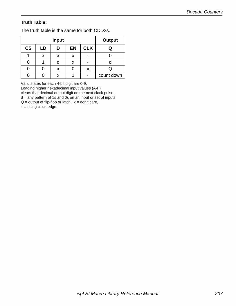
Decade Counters
Truth Table:
The truth table is the same for both CDD2s.
Valid states for each 4-bit digit are 0-9.Loading higher hexadecimal input values (A-F)clears that decimal output digit on the next clock pulse.d = any pattern of 1s and 0s on an input or set of inputs,Q = output of flip-flop or latch, x = don’t care,↑ = rising clock edge.
Input Output
CS LD D EN CLK Q
1 x x x ↑ 00 1 d x ↑ d0 0 x 0 x Q0 0 x 1 ↑ count down
ispLSI Macro Library Reference Manual 207
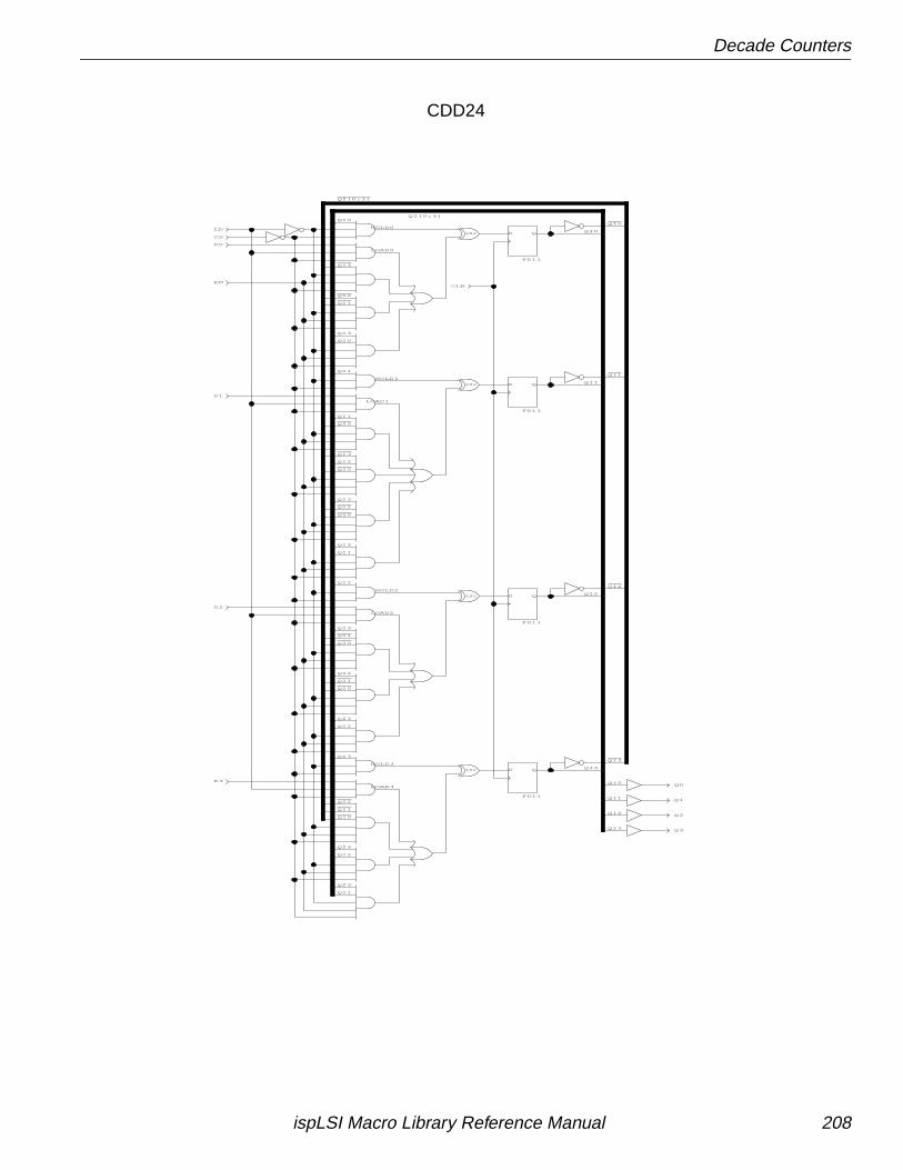
Decade Counters
Q3
Q2
Q1
Q0
QI1
QI2
QI3
QI0
QI2
QI1
QI0
QI1
QI3
QI2
QI3
QI3
QI2
QI3
QI2
QI3
QI2
QI1
QI3
QI3
QI2
QI1
QI1
QI0
QI3
QI[0:3]
QI3
QI0
QI0
QI3
QI1
QI2
QI0
QI2
QI1
QI0
QI1
QI0
QI3
QI2
QI1
QI0
QI2
QI0
QI3
QI0
QI1
QI[0:3]
LX2
LX2
LX2
LX2
CLK
D2
D0
CS
LD
LOAD3
QD
FD11
LOAD2
QD
FD11
LOAD1
QD
FD11
LOAD0
QD
FD11
HOLD1
HOLD0
HOLD2
HOLD3
EN
D1
D3
CDD24
ispLSI Macro Library Reference Manual 208
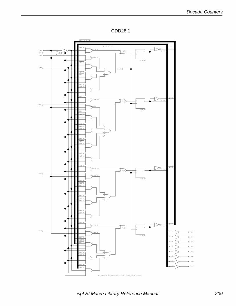
Decade Counters
Q7
Q6
Q5
Q4
Q3
Q2
Q1
Q0
QI1
QI2
QI3
QI4
QI5
QI6
QI7
QI0
QI2
QI1
QI0
QI0
QI1
QI3
QI2
QI3
QI3
QI2
QI3
QI2
QI3
QI2
QI1
QI3
QI3
QI2
QI1
QI1
QI0
QI3
QI[0:7]
QI3
QI0
QI3
QI1
QI2
QI0
QI2
QI1
QI0
QI1
QI0
QI3
QI2
QI1
QI0
QI2
QI0
QI3
QI0
QI1
QI[0:7]
LX2
LX2
LX2
LX2
D3
D1
EN
HOLD3
TMLATTICE Semiconductor Corporation
HOLD2
HOLD0
HOLD1
QD
FD11
LOAD0
QD
FD11
LOAD1
QD
FD11
LOAD2
QD
FD11
LOAD3
LD
CS
D0
D2
CLK
CDD28.1
ispLSI Macro Library Reference Manual 209
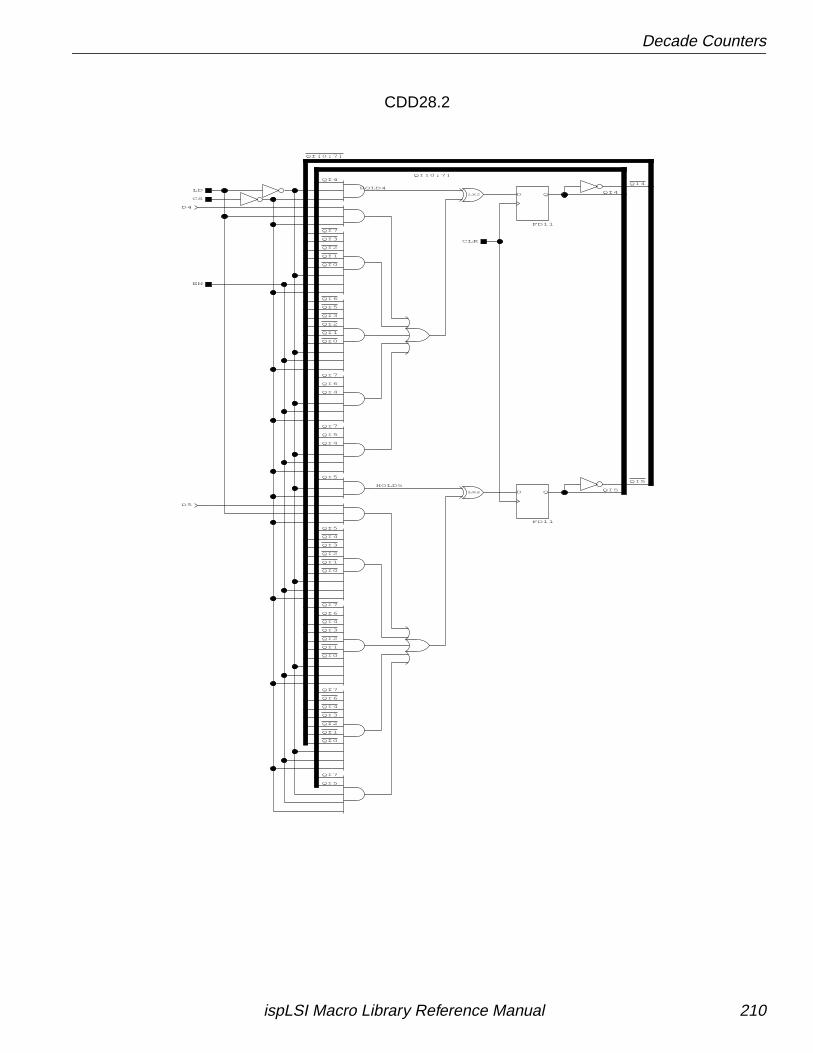
Decade Counters
QI[0:7]
QI7
QI4
QI3
QI2
QI1
QI0
QI4
QI3
QI2
QI1
QI0
QI4
QI3
QI2
QI1
QI0
QI6
QI5
QI6
QI5
QI3
QI2
QI1
QI0
QI7
QI3
QI2
QI1
QI0
QI4
LX2
LX2
CLK
EN
LD
CS
QI[0:7]
QI6
QI5
QI5
QI7
QI7
QI5
QI5
QI7
QI5
QI4
QI7
QI6
QI4
QI4
QI4
QD
FD11
QD
FD11
HOLD4
HOLD5
D4
D5
CDD28.2
ispLSI Macro Library Reference Manual 210
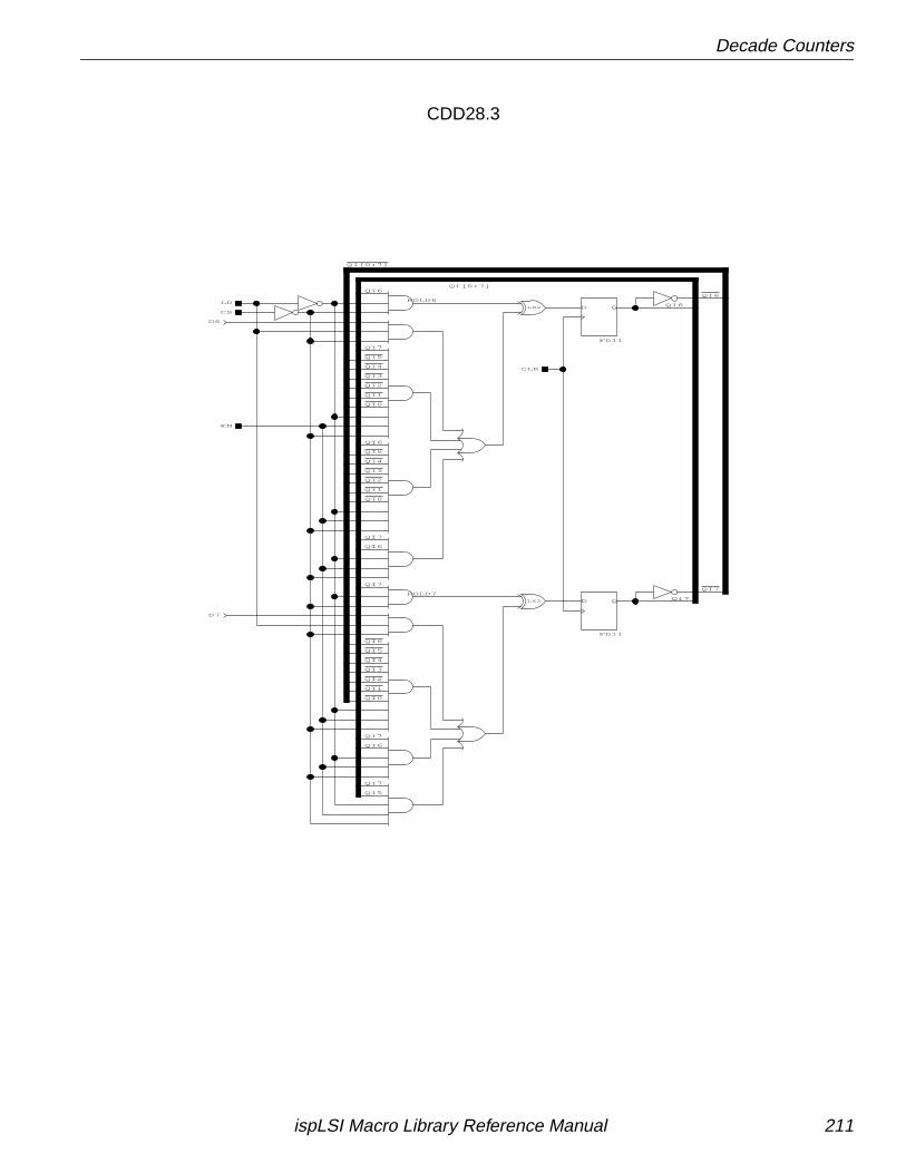
Decade Counters
QI[0:7]
QI6
QI7
QI7
QI5
QI7
QI7
QI6
QI7
QI6
QI7
QI6
QI6
LX2
LX2
CLK
LD
EN
QI[0:7]
QI6
QI5
QI4
QI3
QI2
QI1
QI0
QI3
QI2
QI1
QI0
QI7
QI5
QI4
QI5
QI4
QI3
QI2
QI1
QI0
QI6
QD
FD11
QD
FD11
HOLD7
HOLD6
CS
D6
D7
CDD28.3
ispLSI Macro Library Reference Manual 211
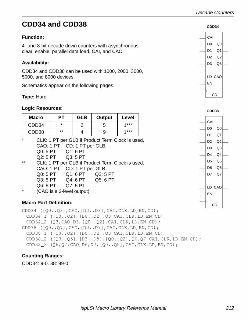
Decade Counters
CDD34 and CDD38
Function:
4- and 8-bit decade down counters with asynchronousclear, enable, parallel data load, CAI, and CAO.
Availability:
CDD34 and CDD38 can be used with 1000, 2000, 3000,5000, and 8000 devices.
Schematics appear on the following pages.
Type: Hard
Logic Resources:
* CLK: 1 PT per GLB if Product Term Clock is used.CAO: 1 PT CD: 1 PT per GLB.Q0: 5 PT Q1: 6 PTQ2: 5 PT Q3: 5 PT
** CLK: 1 PT per GLB if Product Term Clock is used.CAO: 1 PT CD: 1 PT per GLB.Q0: 5 PT Q1: 6 PT Q2: 5 PTQ3: 5 PT Q4: 6 PT Q5: 6 PTQ6: 5 PT Q7: 5 PT
* (CAO is a 2-level output).
Macro Port Definition:
CDD34 ([Q0..Q3],CAO,[D0..D3],CAI,CLK,LD,EN,CD);CDD34_1 ([Q0..Q2],[D0..D2],Q3,CAI,CLK,LD,EN,CD);CDD34_2 (Q3,CAO,D3,[Q0..Q2],CAI,CLK,LD,EN,CD);
CDD38 ([Q0..Q7],CAO,[D0..D7],CAI,CLK,LD,EN,CD);CDD38_1 ([Q0..Q2],[D0..D2],Q3,CAI,CLK,LD,EN,CD);CDD38_2 ([Q3..Q5],[D3..D5],[Q0..Q2],Q6,Q7,CAI,CLK,LD,EN,CD);CDD38_3 (Q6,Q7,CAO,D6,D7,[Q0..Q5],CAI,CLK,LD,EN,CD);
Counting Ranges:
CDD34: 9-0. 38: 99-0.
Macro PT GLB Output Level
CDD34 * 2 5 1***CDD38 ** 4 9 1***
CDD34
CDD38
CD
CAI
Q0D0
Q1D1
Q2D2
Q3D3
EN
LD CAO
CD
CAI
Q0D0
Q1D1
Q2D2
Q3D3
Q4D4
Q5D5
Q6D6
EN
LD CAO
D7 Q7
ispLSI Macro Library Reference Manual 212
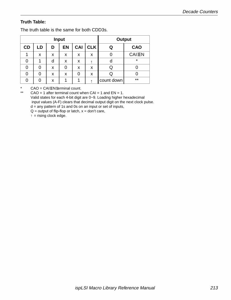
Decade Counters
Truth Table:
The truth table is the same for both CDD3s.
* CAO = CAI⋅EN⋅terminal count.** CAO = 1 after terminal count when CAI = 1 and EN = 1.
Valid states for each 4-bit digit are 0~9. Loading higher hexadecimal input values (A-F) clears that decimal output digit on the next clock pulse.d = any pattern of 1s and 0s on an input or set of inputs,Q = output of flip-flop or latch, x = don’t care,↑ = rising clock edge.
Input Output
CD LD D EN CAI CLK Q CAO
1 x x x x x 0 CAI⋅EN0 1 d x x ↑ d *0 0 x 0 x x Q 00 0 x x 0 x Q 00 0 x 1 1 ↑ count down **
ispLSI Macro Library Reference Manual 213
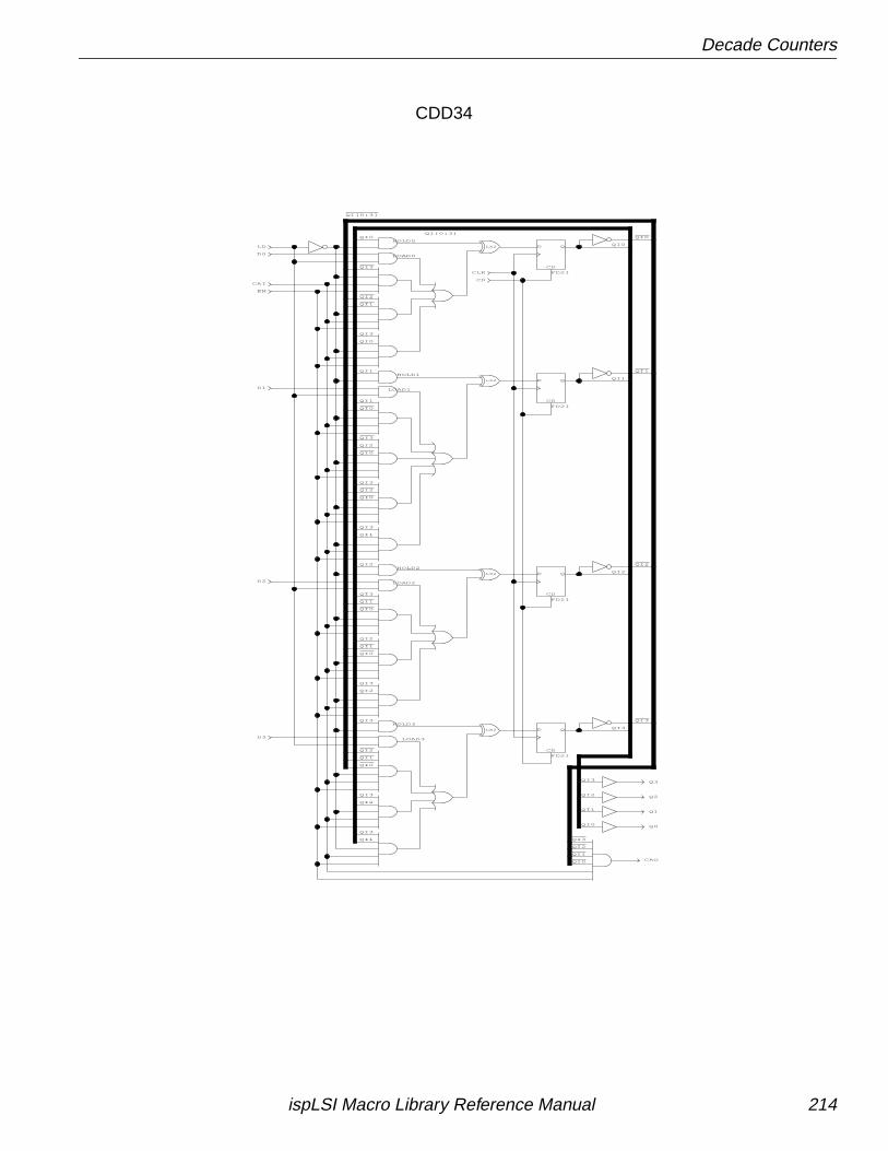
Decade Counters
QI0
QI1
QI2
QI3
QI3
QI2
QI1
QI0
QI3
QI0
QI1
QI1
QI3
QI2
QI2
QI2
QI1
QI3
QI3
QI3
QI3
QI2
QI3
QI3
QI2
QI1
QI0QI[0:3]
QI0
QI3
QI1
QI2
QI2
QI0
QI3
QI0
QI2
QI0
QI1
QI1
QI0
QI0
QI1
QI2
QI3
QI0
QI1
QI[0:3]
QI3
QI2
QI1
QI0 CAO
Q3
Q2
Q1
Q0
LX2
LX2
LX2
LX2
CLK
D3
D2
D1
D0
LD
HOLD2
HOLD1
HOLD0
HOLD3
CD
QD
FD21
LOAD0
CD
QD
FD21
LOAD1
CD
QD
FD21
LOAD2
CD
QD
FD21
LOAD3
CAI
EN
CD
CDD34
ispLSI Macro Library Reference Manual 214
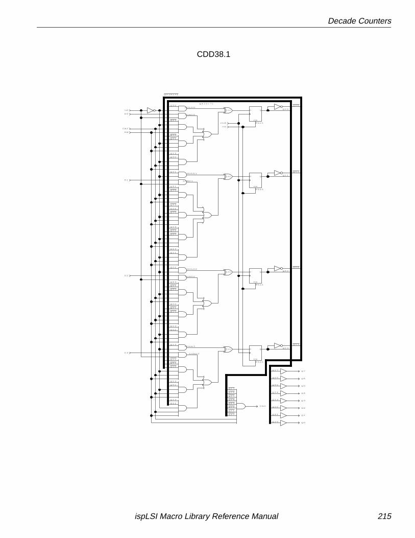
Decade Counters
QI3
QI2
QI1
QI[0:7]
QI3
QI2
QI1
QI3
QI0
QI2
QI0
QI1
QI0
QI1
QI0
QI1
QI2
QI0
QI0
QI0
QI6
QI3
QI2
QI1
QI0
QI4
QI5
QI7
QI3
QI2
QI1
QI0
QI5
QI6
QI7
QI[0:7]QI0
QI1
QI2
QI3
QI3
QI2
QI3
QI3
QI3
QI3
QI1
QI2
QI2
QI2
QI3
QI1
QI1
QI0
QI3
QI0
QI1
QI2
QI3
QI4
CAO
Q0
Q1
Q2
Q3
Q4
Q5
Q6
Q7
LX2
LX2
LX2
LX2
CD
EN
CAI
LOAD3
CD
QD
FD21
LOAD2
CD
QD
FD21
LOAD1
CD
QD
FD21
LOAD0
CD
QD
FD21
HOLD3
HOLD0
HOLD1
HOLD2
LD
D0
D1
D2
D3
CLK
CDD38.1
ispLSI Macro Library Reference Manual 215
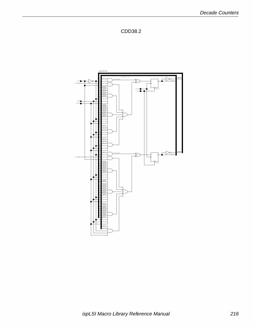
Decade Counters
QI4
QI0
QI1
QI3
QI2
QI7
QI0
QI1
QI2
QI3
QI4
QI6
QI4
QI3
QI2
QI1
QI0
QI7
QI4
QI3
QI2
QI1
QI0
QI6
QI5
QI3
QI2
QI1
QI0
QI5
QI[0:7]
LX2
LX2
CLK
CD
EN
CAI
LD
CD
QD
FD21
HOLD5
HOLD4
CD
QD
FD21
QI4
QI6
QI7
QI5
QI4
QI4
QI4
QI5
QI7
QI5
QI6
QI7
QI5
QI7
QI5
QI[0:7]
D4
D5
CDD38.2
ispLSI Macro Library Reference Manual 216
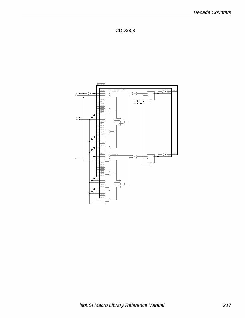
Decade Counters
QI[0:7]
QI6
QI5
QI4
QI3
QI2
QI1
QI0
QI7
QI5
QI4
QI2
QI3
QI1
QI0
QI5
QI4
QI3
QI1
QI2
QI0
QI6
LX2
LX2
CLK
CD
EN
CAI
LD
QI[0:7]
QI7
QI7
QI6
QI7
QI5
QI7
QI7
QI6
QI6
QI7
QI6
QI6
CD
QD
FD21
CD
QD
FD21
HOLD6
HOLD7
D6
D7
CDD38.3
ispLSI Macro Library Reference Manual 217
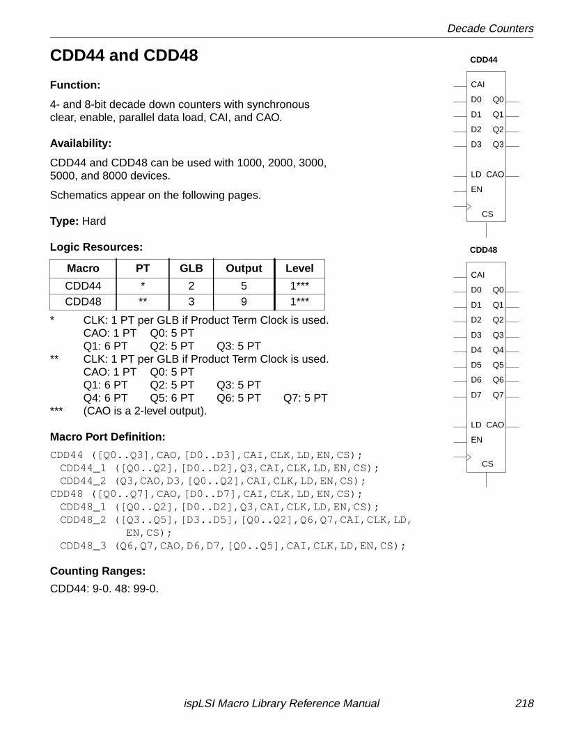
Decade Counters
CDD44 and CDD48
Function:
4- and 8-bit decade down counters with synchronousclear, enable, parallel data load, CAI, and CAO.
Availability:
CDD44 and CDD48 can be used with 1000, 2000, 3000,5000, and 8000 devices.
Schematics appear on the following pages.
Type: Hard
Logic Resources:
* CLK: 1 PT per GLB if Product Term Clock is used.CAO: 1 PT Q0: 5 PTQ1: 6 PT Q2: 5 PT Q3: 5 PT
** CLK: 1 PT per GLB if Product Term Clock is used.CAO: 1 PT Q0: 5 PTQ1: 6 PT Q2: 5 PT Q3: 5 PTQ4: 6 PT Q5: 6 PT Q6: 5 PT Q7: 5 PT
*** (CAO is a 2-level output).
Macro Port Definition:
CDD44 ([Q0..Q3],CAO,[D0..D3],CAI,CLK,LD,EN,CS);CDD44_1 ([Q0..Q2],[D0..D2],Q3,CAI,CLK,LD,EN,CS);CDD44_2 (Q3,CAO,D3,[Q0..Q2],CAI,CLK,LD,EN,CS);
CDD48 ([Q0..Q7],CAO,[D0..D7],CAI,CLK,LD,EN,CS);CDD48_1 ([Q0..Q2],[D0..D2],Q3,CAI,CLK,LD,EN,CS);CDD48_2 ([Q3..Q5],[D3..D5],[Q0..Q2],Q6,Q7,CAI,CLK,LD,
EN,CS);CDD48_3 (Q6,Q7,CAO,D6,D7,[Q0..Q5],CAI,CLK,LD,EN,CS);
Counting Ranges:
CDD44: 9-0. 48: 99-0.
Macro PT GLB Output Level
CDD44 * 2 5 1***CDD48 ** 3 9 1***
CDD44
CDD48
CS
CAI
Q0D0
Q1D1
Q2D2
Q3D3
EN
LD CAO
CS
CAI
Q0D0
Q1D1
Q2D2
Q3D3
Q4D4
Q5D5
Q6D6
EN
LD CAO
D7 Q7
ispLSI Macro Library Reference Manual 218
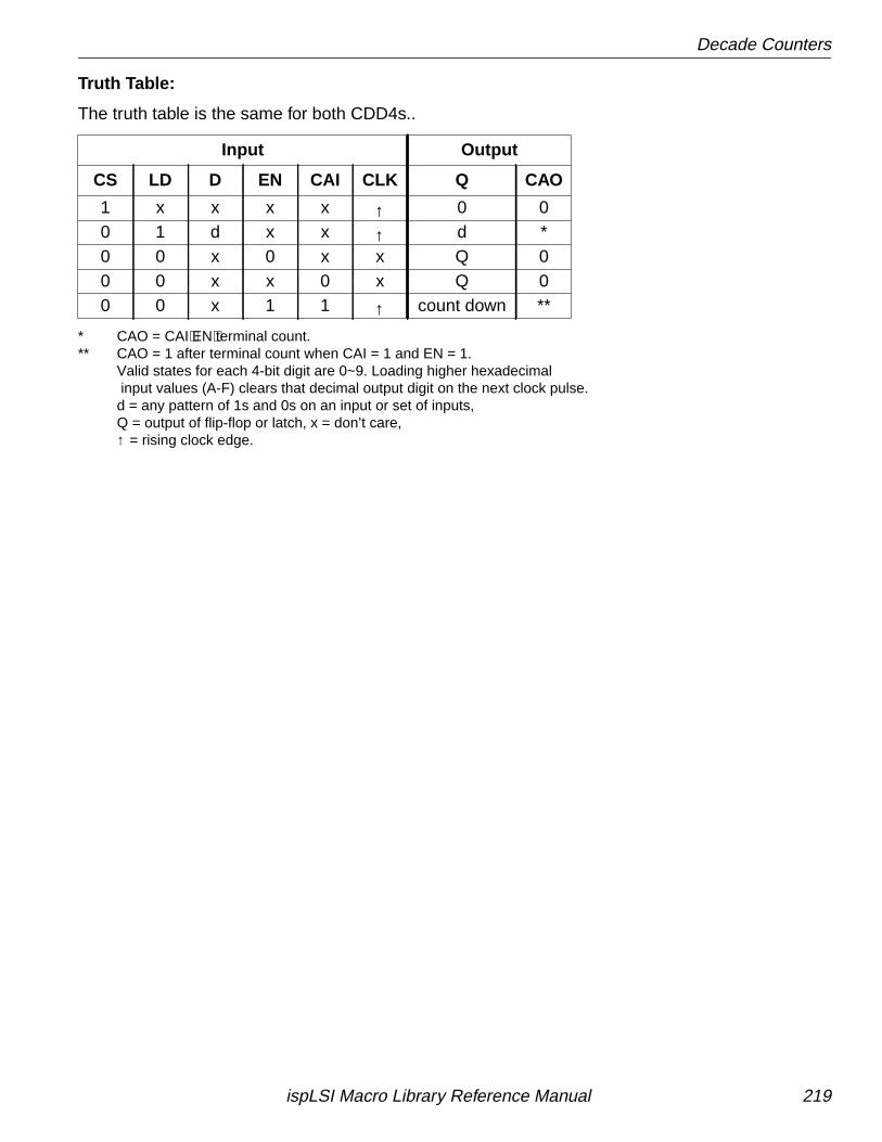
Decade Counters
Truth Table:
The truth table is the same for both CDD4s..
* CAO = CAI⋅EN⋅terminal count.** CAO = 1 after terminal count when CAI = 1 and EN = 1.
Valid states for each 4-bit digit are 0~9. Loading higher hexadecimal input values (A-F) clears that decimal output digit on the next clock pulse.d = any pattern of 1s and 0s on an input or set of inputs,Q = output of flip-flop or latch, x = don’t care,↑ = rising clock edge.
Input Output
CS LD D EN CAI CLK Q CAO
1 x x x x ↑ 0 00 1 d x x ↑ d *0 0 x 0 x x Q 00 0 x x 0 x Q 00 0 x 1 1 ↑ count down **
ispLSI Macro Library Reference Manual 219
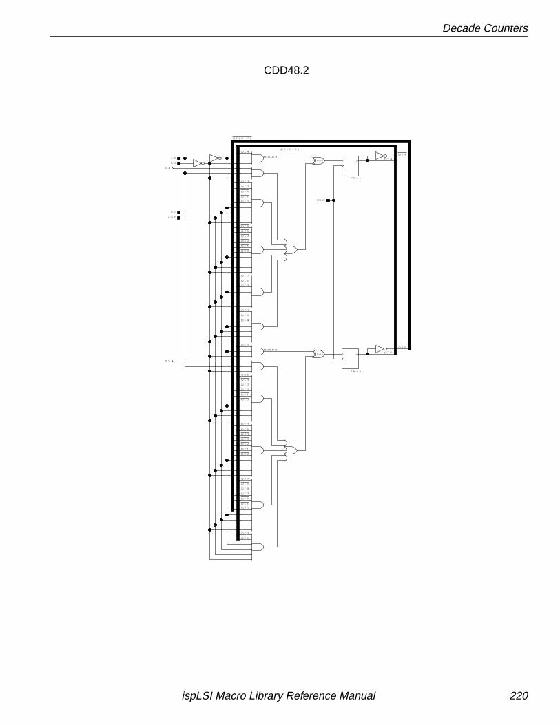
Decade Counters
QI5
QI4
QI4
QI4
QI5
QI7
QI5
QI5
QI6
QI7
QI5
QI7
QI4
QI6
QI7
QI[0:7]
QI4
QI0
QI2
QI1
QI3
QI7
QI0
QI1
QI2
QI3
QI5
QI6
QI0
QI1
QI2
QI3
QI4
QI0
QI1
QI2
QI3
QI4
QI7
QI0
QI1
QI2
QI3
QI4
QI6
QI5
QI[0:7]
LX2
LX2
CLK
LD
CS
EN
CAI
QD
FD11
HOLD4
QD
FD11
HOLD5
D4
D5
CDD48.2
ispLSI Macro Library Reference Manual 220
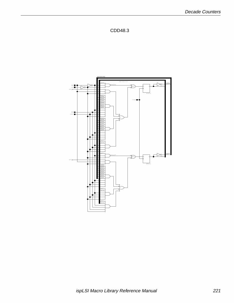
Decade Counters
QI[0:7]
QI0
QI1
QI2
QI3
QI4
QI5
QI6
QI7
QI0
QI1
QI2
QI3
QI4
QI5
QI0
QI1
QI2
QI3
QI4
QI5
QI6
LX2
LX2
CLK
EN
CAI
LD
CS
QI[0:7]
QI7
QI5
QI7
QI6
QI7
QI7
QI7
QI6
QI6
QI7
QI6
QI6
QD
FD11
HOLD7
QD
FD11
HOLD6
D6
D7
CDD48.3
ispLSI Macro Library Reference Manual 221
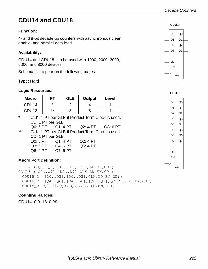
Decade Counters
CDU14 and CDU18
Function:
4- and 8-bit decade up counters with asynchronous clear,enable, and parallel data load.
Availability:
CDU14 and CDU18 can be used with 1000, 2000, 3000,5000, and 8000 devices.
Schematics appear on the following pages.
Type: Hard
Logic Resources:
* CLK: 1 PT per GLB if Product Term Clock is used.CD: 1 PT per GLB.Q0: 5 PT Q1: 4 PT Q2: 4 PT Q3: 6 PT
** CLK: 1 PT per GLB if Product Term Clock is used.CD: 1 PT per GLB.Q0: 5 PT Q1: 4 PT Q2: 4 PTQ3: 6 PT Q4: 6 PT Q5: 4 PTQ6: 4 PT Q7: 6 PT
Macro Port Definition:
CDU14 ([Q0..Q3],[D0..D3],CLK,LD,EN,CD);CDU18 ([Q0..Q7],[D0..D7],CLK,LD,EN,CD);
CDU18_1 ([Q0..Q3],[D0..D3],CLK,LD,EN,CD);CDU18_2 ([Q4..Q6],[D4..D6],[Q0..Q3],Q7,CLK,LD,EN,CD);CDU18_3 (Q7,D7,[Q0..Q6],CLK,LD,EN,CD);
Counting Ranges:
CDU14: 0-9. 18: 0-99.
Macro PT GLB Output Level
CDU14 * 2 4 1CDU18 ** 3 8 1
CDU14
CDU18
LD
EN
D3 Q3
D2 Q2
D1 Q1
D0 Q0
CD
Q7D7
LD
EN
D6 Q6
D5 Q5
D4 Q4
D3 Q3
D2 Q2
D1 Q1
D0 Q0
CD
ispLSI Macro Library Reference Manual 222

Decade Counters
Truth Table:
The truth table is the same for both CDU1s.
Valid states for each 4-bit digit are 0-9.Loading higher hexadecimal input values (A-F)clears that decimal output digit on the next clock pulse.d = any pattern of 1s and 0s on an input or set of inputs,Q = output of flip-flop or latch, x = don’t care,↑ = rising clock edge.
Input Output
CD LD D EN CLK Q
1 x x x x 00 1 d x ↑ d0 0 x 0 x Q0 0 x 1 ↑ count up
ispLSI Macro Library Reference Manual 223
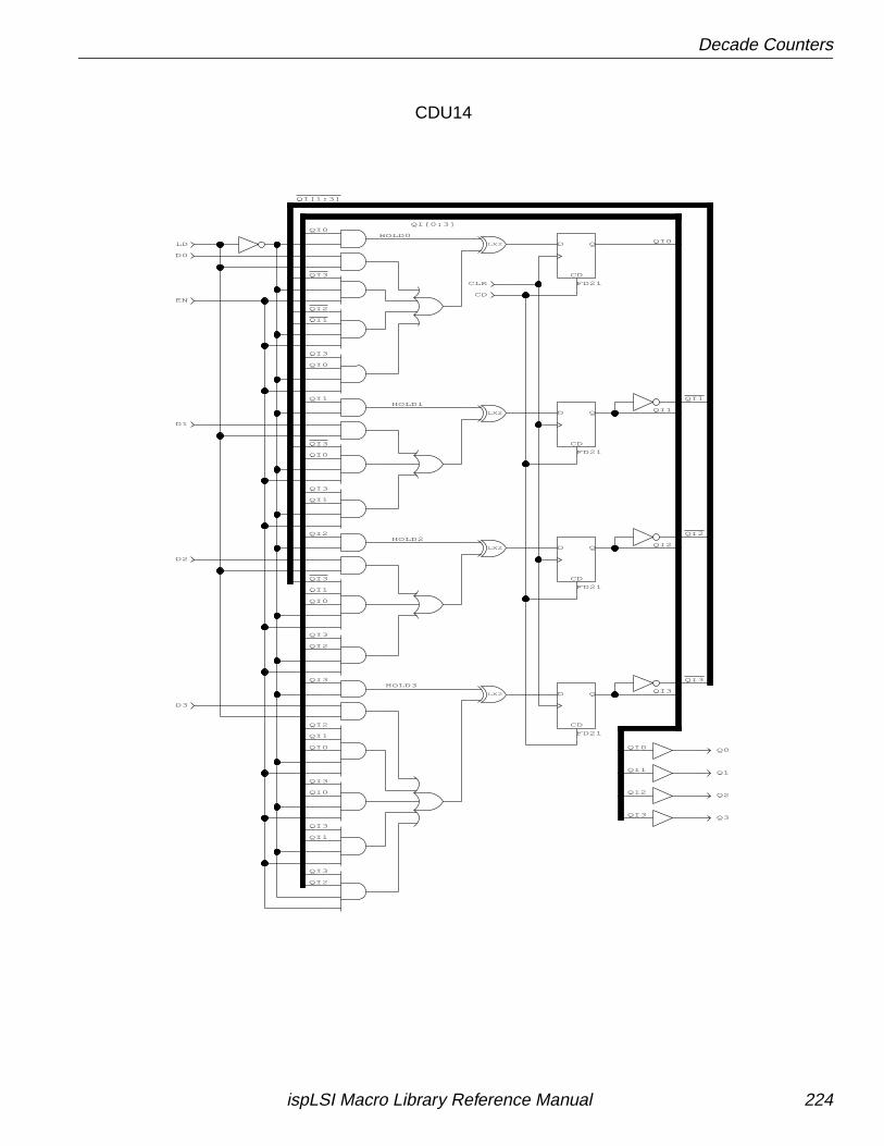
Decade Counters
QI1
QI[1:3]
QI3
QI1
QI2
QI3
QI2
QI3
QI3
QI2
QI1
QI[0:3]QI0
QI0
QI1
QI0
QI0
QI3
QI2
QI3
QI1
QI3
QI2
QI0
QI3
QI0
QI1
QI3
QI1
QI2
QI1
QI3
QI3
QI0
QI3
QI0
QI1
QI2
QI3
QI2
Q0
Q1
Q2
Q3
D3
D2
D1
D0
EN
LD
CD
QD
FD21CLK
CD
HOLD0
HOLD3
HOLD2
HOLD1
CD
QD
FD21
CD
QD
FD21
CD
QD
FD21
LX2
LX2
LX2
LX2
CDU14
ispLSI Macro Library Reference Manual 224
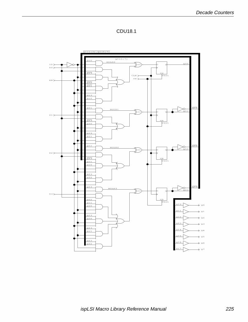
Decade Counters
QI6
QI5
QI4
QI3
QI2
QI1
QI0
QI7
QI0
QI3
QI1
QI3
QI1
QI3
QI0
QI1
QI2
QI1
QI2
QI1
QI0
QI0
QI0
QI2
QI2
QI0
QI3
QI0
QI2
QI3
QI1
QI3
QI3
QI[0:7]
QI3
Q0
Q1
Q2
Q3
Q4
Q5
Q6
Q7
CD
QD
FD21
QI3
QI3
QI1
QI2
QI3
QI2
QI3
QI1
QI[1:3],QI[5:7]
CD
QD
FD21
CD
QD
FD21
HOLD1
HOLD2
HOLD3
HOLD0
CD
CLK
CD
QD
FD21
LD
EN
D0
D1
D2
D3
LX2
LX2
LX2
LX2
CDU18.1
ispLSI Macro Library Reference Manual 225
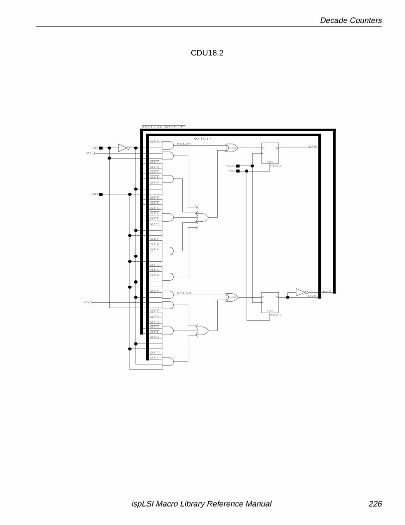
Decade Counters
QI2
QI1
QI6
QI5
QI2
QI1
QI7
QI2
QI1
QI7
QI[1:3],QI[5:7]
QI5
D5
D4
HOLD4
HOLD5
CD
QD
FD21
CD
QD
FD21
LD
EN
CLK
CD
LX2
LX2
QI0
QI3
QI0
QI7
QI6
QI4
QI7
QI5
QI4
QI5
QI4
QI3
QI0
QI7
QI5
QI3
QI4QI[0:7]
QI4
QI5
CDU18.2
ispLSI Macro Library Reference Manual 226
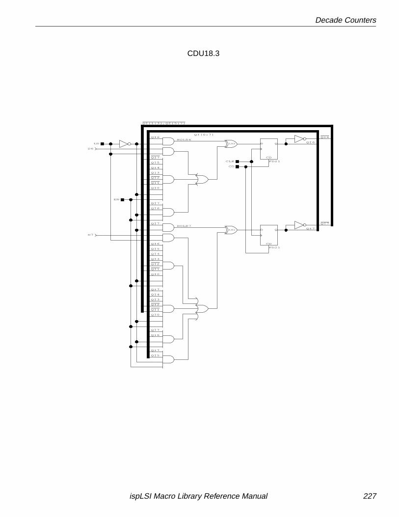
Decade Counters
QI1
QI6
QI7
QI2
QI2
QI1
QI7
QI1
QI2
QI[1:3],QI[5:7]
QI7
QI7
QI5
QI6
QI7
QI4
QI3
QI0
QI7
QI6
QI7
QI6
QI7
QI0
QI6
QI5
QI4
QI3
QI6
QI5
QI4
QI3
QI0
QI[0:7]
D6
HOLD6
HOLD7
CD
QD
FD21
CD
QD
FD21
LD
EN
D7
CD
CLK
LX2
LX2
CDU18.3
ispLSI Macro Library Reference Manual 227
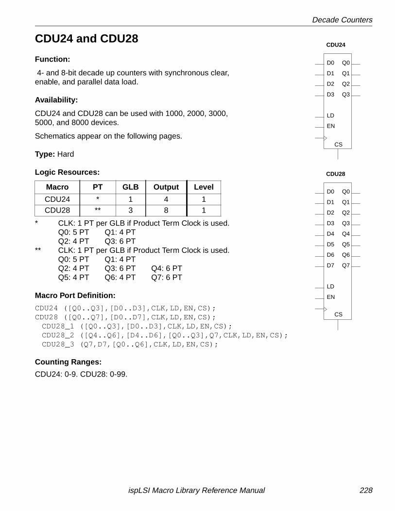
Decade Counters
CDU24 and CDU28
Function:
4- and 8-bit decade up counters with synchronous clear,enable, and parallel data load.
Availability:
CDU24 and CDU28 can be used with 1000, 2000, 3000,5000, and 8000 devices.
Schematics appear on the following pages.
Type: Hard
Logic Resources:
* CLK: 1 PT per GLB if Product Term Clock is used.Q0: 5 PT Q1: 4 PTQ2: 4 PT Q3: 6 PT
** CLK: 1 PT per GLB if Product Term Clock is used.Q0: 5 PT Q1: 4 PTQ2: 4 PT Q3: 6 PT Q4: 6 PTQ5: 4 PT Q6: 4 PT Q7: 6 PT
Macro Port Definition:
CDU24 ([Q0..Q3],[D0..D3],CLK,LD,EN,CS);CDU28 ([Q0..Q7],[D0..D7],CLK,LD,EN,CS);
CDU28_1 ([Q0..Q3],[D0..D3],CLK,LD,EN,CS);CDU28_2 ([Q4..Q6],[D4..D6],[Q0..Q3],Q7,CLK,LD,EN,CS);CDU28_3 (Q7,D7,[Q0..Q6],CLK,LD,EN,CS);
Counting Ranges:
CDU24: 0-9. CDU28: 0-99.
Macro PT GLB Output Level
CDU24 * 1 4 1CDU28 ** 3 8 1
CDU24
CDU28
LD
EN
D3 Q3
D2 Q2
D1 Q1
D0 Q0
CS
Q7D7
LD
EN
D6 Q6
D5 Q5
D4 Q4
D3 Q3
D2 Q2
D1 Q1
D0 Q0
CS
ispLSI Macro Library Reference Manual 228
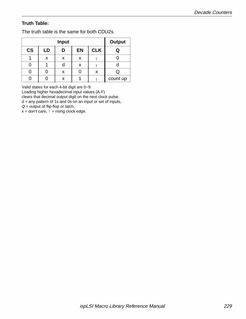
Decade Counters
Truth Table:
The truth table is the same for both CDU2s.
Valid states for each 4-bit digit are 0~9.Loading higher hexadecimal input values (A-F)clears that decimal output digit on the next clock pulse.d = any pattern of 1s and 0s on an input or set of inputs,Q = output of flip-flop or latch,x = don’t care, ↑ = rising clock edge.
Input Output
CS LD D EN CLK Q
1 x x x ↑ 00 1 d x ↑ d0 0 x 0 x Q0 0 x 1 ↑ count up
ispLSI Macro Library Reference Manual 229
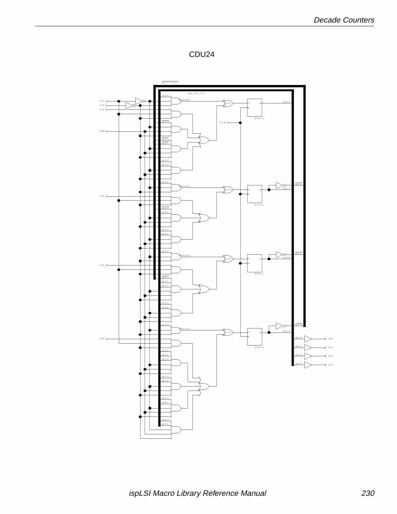
Decade Counters
Q0
Q1
Q2
Q3
QI2
QI1
QI0
QI0
QI2
QI2
QI1
QI0
QI0
QI0
QI1
QI3
QI1
QI3
QI0
QI3
QI0
QI1
QI2
QI3
QI2
QI3
QI0
QI1
QI2
QI3
QI1
QI3
QI[0:3]
QI3
QI3
QI2
QI1
QI2
QI1
QI3
QI3
QI3
QI[1:3]
QI3
EN
CLK
QD
FD11
HOLD3
HOLD0
HOLD1
HOLD2
QD
FD11
QD
FD11
QD
FD11
CS
LD
D1
D0
D2
D3
LX2
LX2
LX2
LX2
CDU24
ispLSI Macro Library Reference Manual 230
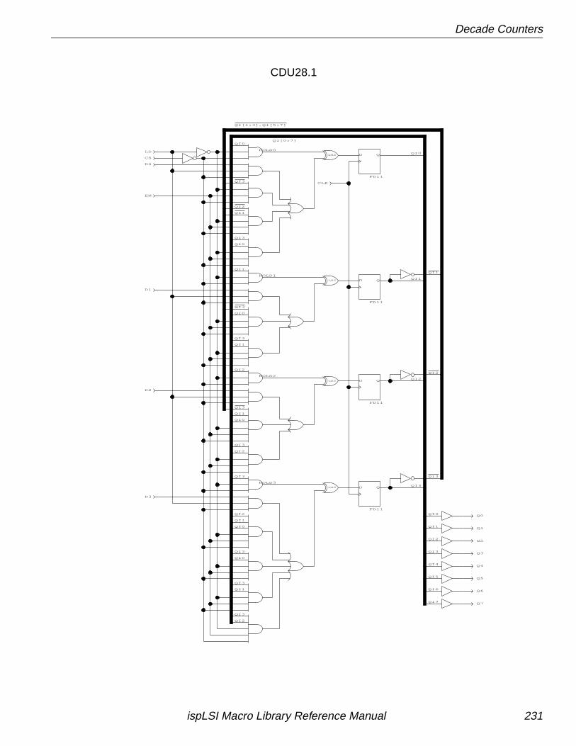
Decade Counters
Q7
Q6
Q5
Q4
Q3
Q2
Q1
Q0
QI6
QI5
QI4
QI3
QI2
QI1
QI0
QI7
QI3
QI[0:7]
QI3
QI1
QI3
QI2
QI1
QI0
QI3
QI2
QI3
QI2
QI3
QI0
QI3
QI1
QI3
QI2
QI1
QI0
QI0
QI0
QI0
QI2
QI1
QI0
QI1
QI2
QI1
QI2
QI1
QI3
QI3
QI3
QI[1:3],QI[5:7]
QI3
D3
D2
D0
D1
LD
CS
QD
FD11
QD
FD11
QD
FD11
HOLD2
HOLD1
HOLD0
HOLD3
QD
FD11
CLK
EN
LX2
LX2
LX2
LX2
CDU28.1
ispLSI Macro Library Reference Manual 231
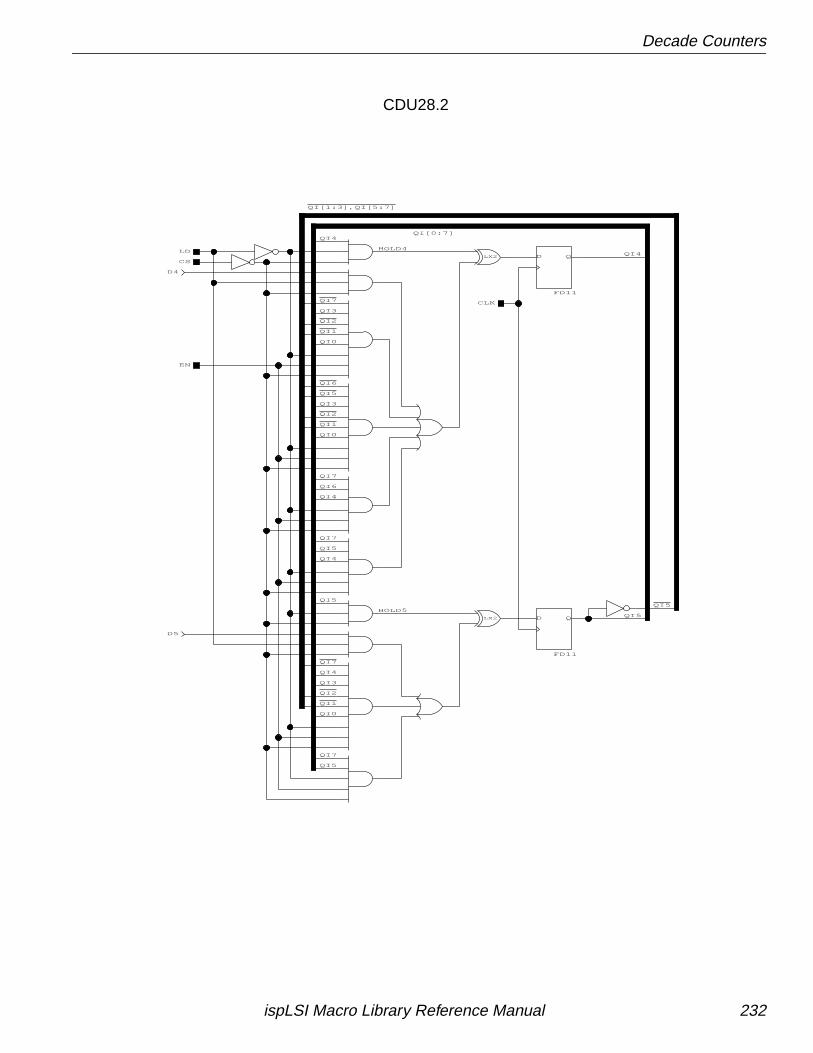
Decade Counters
QI5
QI5
QI0
QI0
QI3
QI4
QI5
QI4
QI7
QI4
QI6
QI7
QI0
QI3
QI3
QI4
QI4
QI[0:7]
QI7
QI5
QI2
QI7
QI1
QI6
QI5
QI2
QI1
QI7
QI2
QI1
QI[1:3],QI[5:7]
QI5
CLK
LD
CS
EN
QD
FD11
QD
FD11
HOLD5
HOLD4
D4
D5
LX2
LX2
CDU28.2
ispLSI Macro Library Reference Manual 232
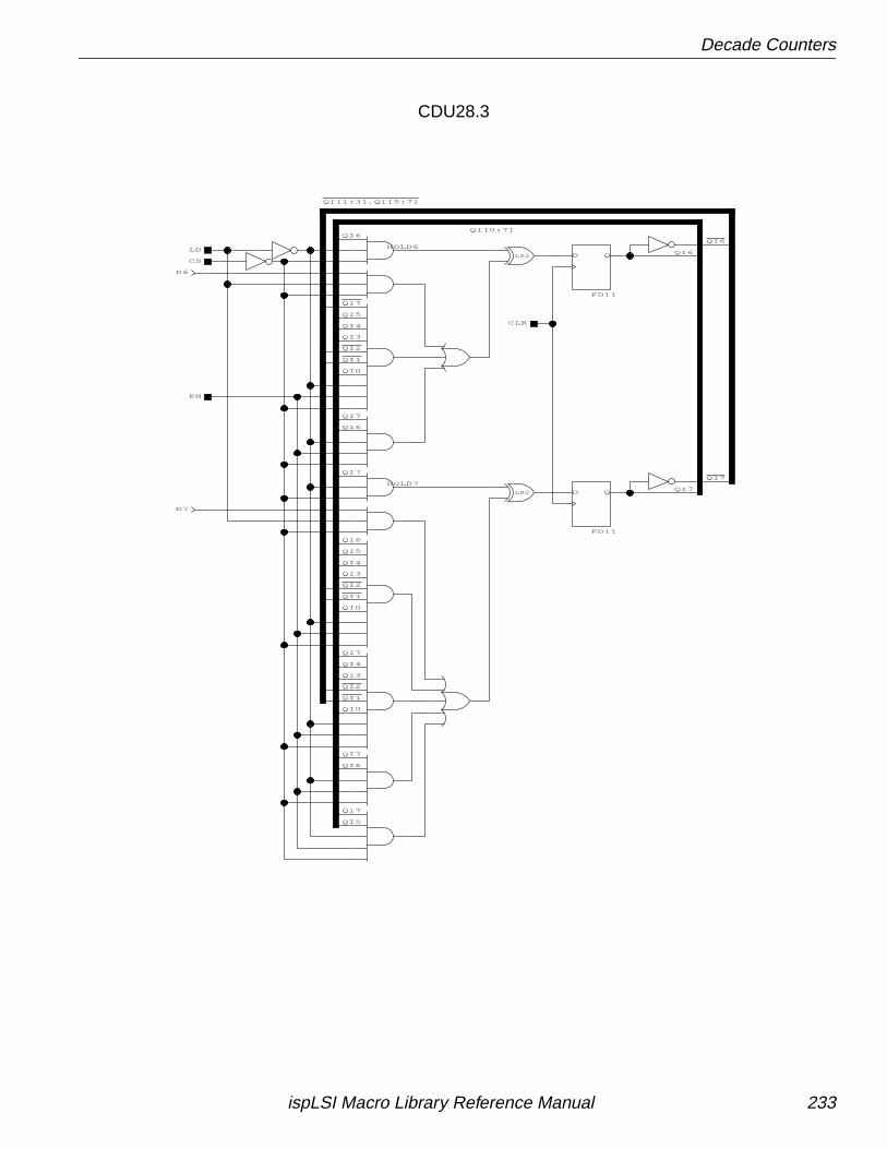
Decade Counters
QI7
QI7
QI[0:7]
QI6
QI7
QI4
QI3
QI0
QI6
QI5
QI4
QI3
QI0
QI7
QI6
QI0
QI3
QI4
QI5
QI6
QI7
QI6
QI7
QI5
QI[1:3],QI[5:7]
QI2
QI1
QI2
QI1
QI1
QI2
QI7
QI6
QI7
D6
D7
CS
LD
EN
QD
FD11
HOLD6
QD
FD11
HOLD7
CLK
LX2
LX2
CDU28.3
ispLSI Macro Library Reference Manual 233
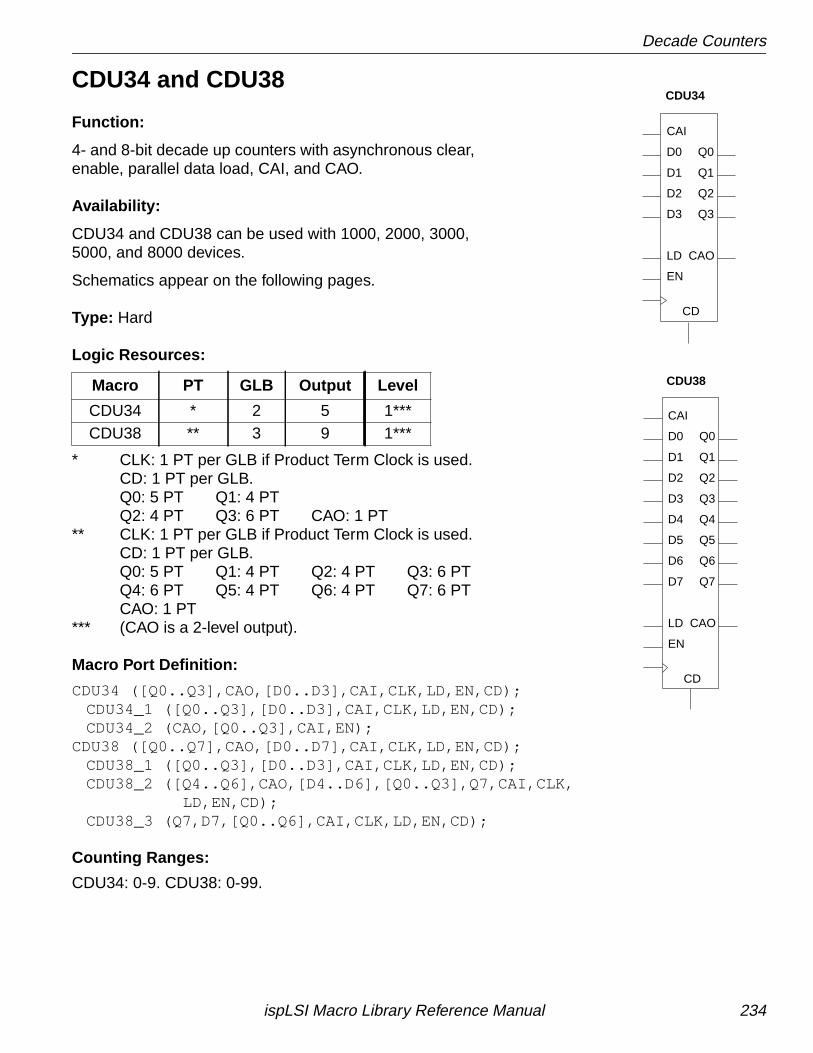
Decade Counters
CDU34 and CDU38
Function:
4- and 8-bit decade up counters with asynchronous clear,enable, parallel data load, CAI, and CAO.
Availability:
CDU34 and CDU38 can be used with 1000, 2000, 3000,5000, and 8000 devices.
Schematics appear on the following pages.
Type: Hard
Logic Resources:
* CLK: 1 PT per GLB if Product Term Clock is used.CD: 1 PT per GLB.Q0: 5 PT Q1: 4 PTQ2: 4 PT Q3: 6 PT CAO: 1 PT
** CLK: 1 PT per GLB if Product Term Clock is used.CD: 1 PT per GLB.Q0: 5 PT Q1: 4 PT Q2: 4 PT Q3: 6 PTQ4: 6 PT Q5: 4 PT Q6: 4 PT Q7: 6 PTCAO: 1 PT
*** (CAO is a 2-level output).
Macro Port Definition:
CDU34 ([Q0..Q3],CAO,[D0..D3],CAI,CLK,LD,EN,CD);CDU34_1 ([Q0..Q3],[D0..D3],CAI,CLK,LD,EN,CD);CDU34_2 (CAO,[Q0..Q3],CAI,EN);
CDU38 ([Q0..Q7],CAO,[D0..D7],CAI,CLK,LD,EN,CD);CDU38_1 ([Q0..Q3],[D0..D3],CAI,CLK,LD,EN,CD);CDU38_2 ([Q4..Q6],CAO,[D4..D6],[Q0..Q3],Q7,CAI,CLK,
LD,EN,CD);CDU38_3 (Q7,D7,[Q0..Q6],CAI,CLK,LD,EN,CD);
Counting Ranges:
CDU34: 0-9. CDU38: 0-99.
Macro PT GLB Output Level
CDU34 * 2 5 1***CDU38 ** 3 9 1***
CDU34
CDU38
CD
CAI
Q0D0
Q1D1
Q2D2
Q3D3
EN
LD CAO
CD
CAI
Q0D0
Q1D1
Q2D2
Q3D3
Q4D4
Q5D5
Q6D6
EN
LD CAO
D7 Q7
ispLSI Macro Library Reference Manual 234
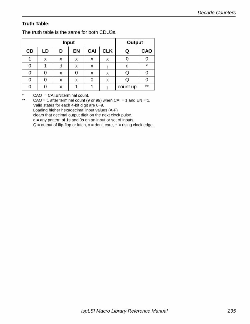
Decade Counters
Truth Table:
The truth table is the same for both CDU3s.
* CAO = CAI⋅EN⋅terminal count.** CAO = 1 after terminal count (9 or 99) when CAI = 1 and EN = 1.
Valid states for each 4-bit digit are 0~9.Loading higher hexadecimal input values (A-F)clears that decimal output digit on the next clock pulse.d = any pattern of 1s and 0s on an input or set of inputs,Q = output of flip-flop or latch, x = don’t care, ↑ = rising clock edge.
Input Output
CD LD D EN CAI CLK Q CAO
1 x x x x x 0 00 1 d x x ↑ d *0 0 x 0 x x Q 00 0 x x 0 x Q 00 0 x 1 1 ↑ count up **
ispLSI Macro Library Reference Manual 235
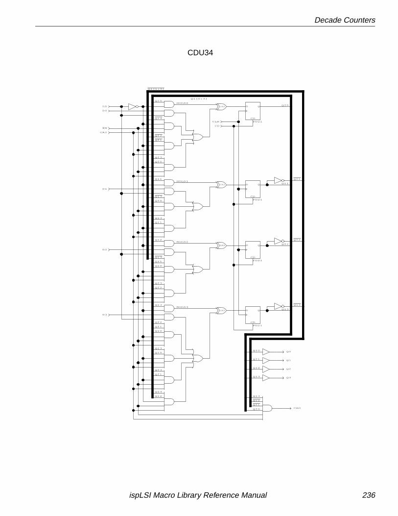
Decade Counters
QI3
QI2
QI1
QI0
QI2
QI0
QI2
QI0
QI1
QI0
QI3
QI1
QI3
QI2
QI3
QI1
QI0
QI3
QI1
QI2
QI3
QI0
QI3
QI0
QI1
QI2
QI0
QI3
QI[0:3]
QI0
QI1
QI3
QI3
QI1
QI2
QI2
QI3
QI3
QI1
QI3
QI[1:3]
QI1
QI3
QI2
Q0
Q1
Q2
Q3
CD
CAI
CAO
HOLD0
CD
QD
FD21
HOLD1
HOLD2
HOLD3
CD
QD
FD21
CD
QD
FD21
CD
QD
FD21
EN
LD
D1
D0
D3
D2
CLK
LX2
LX2
LX2
LX2
CDU34
ispLSI Macro Library Reference Manual 236
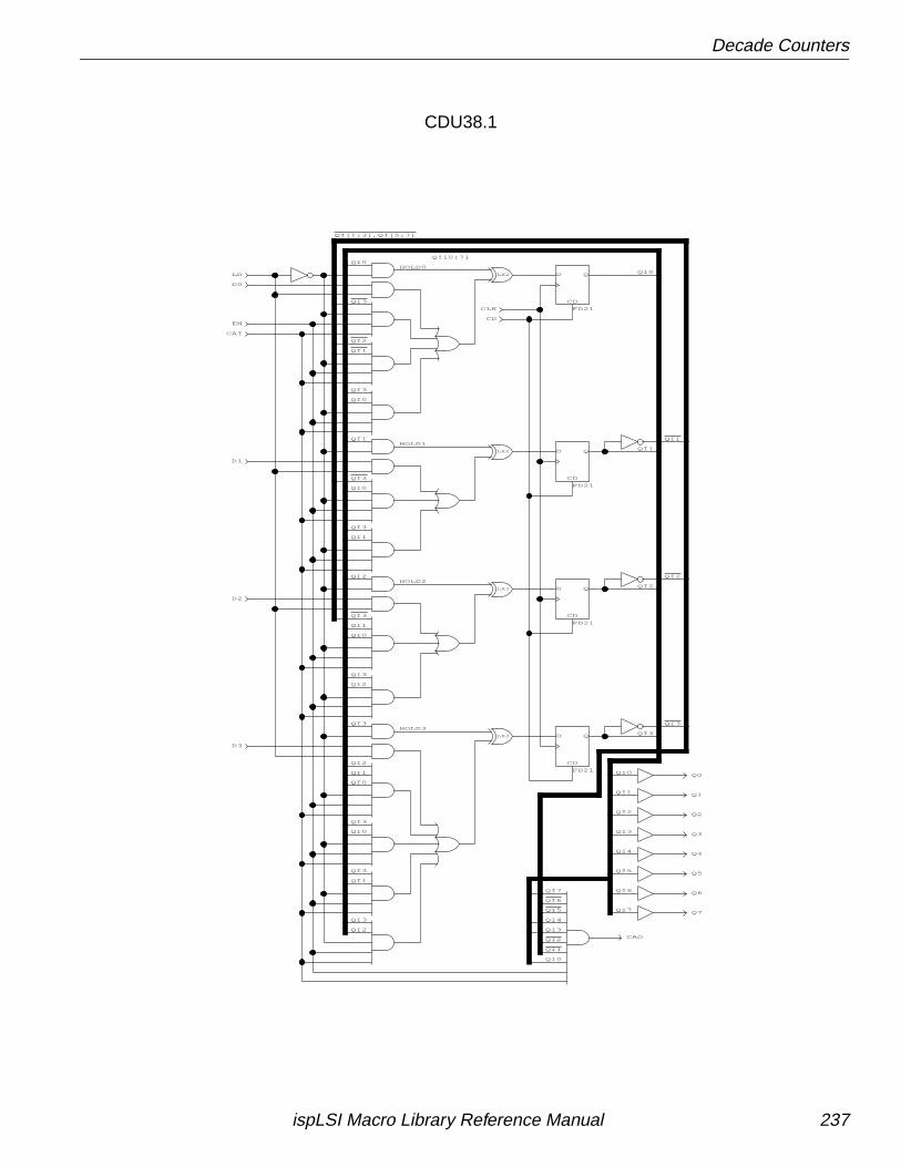
Decade Counters
QI7
QI6
QI5
QI3
QI2
QI1
QI0
QI4
QI2
QI[0:7]QI0
QI1
QI0
QI3
QI1
QI3
QI2
QI3
QI2
QI1
QI0
QI3
QI1
QI2
QI3
QI0
QI3
QI0
QI1
QI2
QI0
QI3
QI0
QI1
QI3
QI7
QI0
QI3
QI4
QI5
QI1
QI2
QI[1:3],QI[5:7]
QI3
QI3
QI1
QI2
QI3
QI1
QI2
QI3
QI6
CD
QD
FD21
Q4
Q3
Q2
Q1
Q0
Q5
Q6
Q7
CAO
CLK
D2
D3
D0
D1
LD
EN
CD
QD
FD21
CD
QD
FD21
HOLD3
HOLD2
HOLD1
CD
QD
FD21
HOLD0
CAI
CD
LX2
LX2
LX2
LX2
CDU38.1
ispLSI Macro Library Reference Manual 237
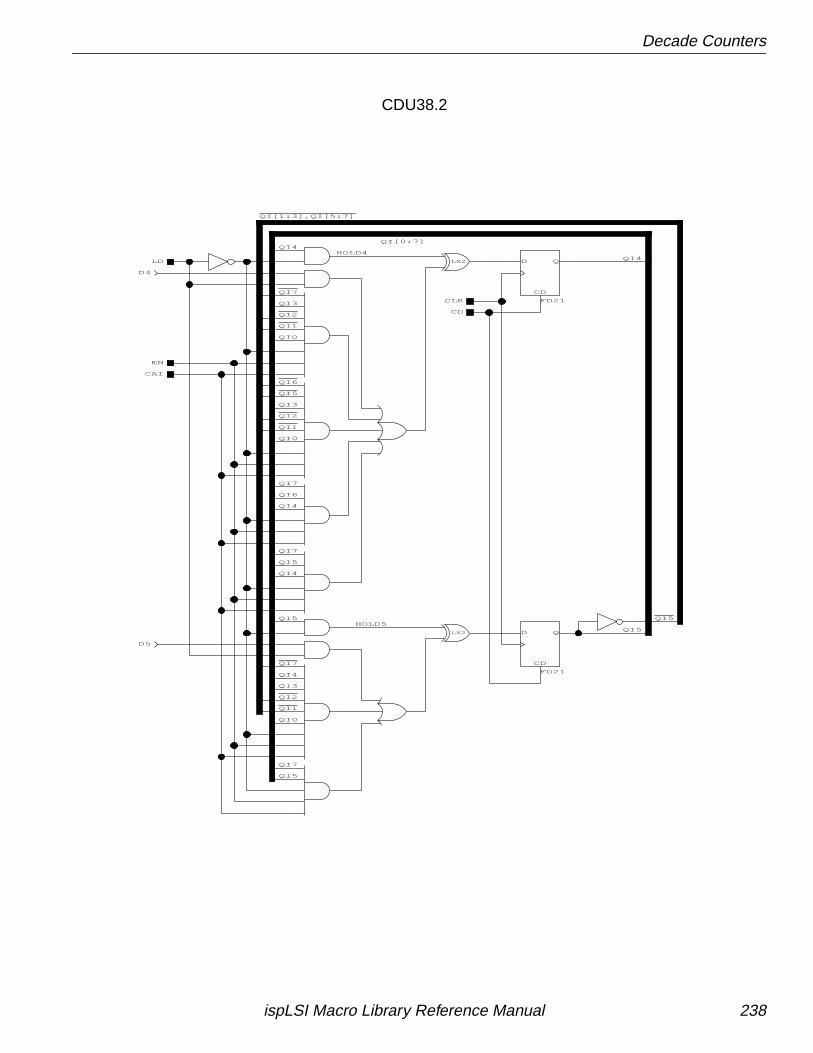
Decade Counters
QI7
QI1
QI2
QI7
QI1
QI2
QI5
QI6
QI1
QI2
QI[1:3],QI[5:7]
QI5
QI4
QI4
QI5
QI[0:7]
QI3
QI0
QI3
QI0
QI7
QI6
QI4
QI7
QI5
QI4
QI5
QI4
QI3
QI0
QI7
QI5
D5
D4
CLK
CD
QD
FD21
CD
QD
FD21
HOLD5
HOLD4
CD
LD
CAI
EN
LX2
LX2
CDU38.2
ispLSI Macro Library Reference Manual 238
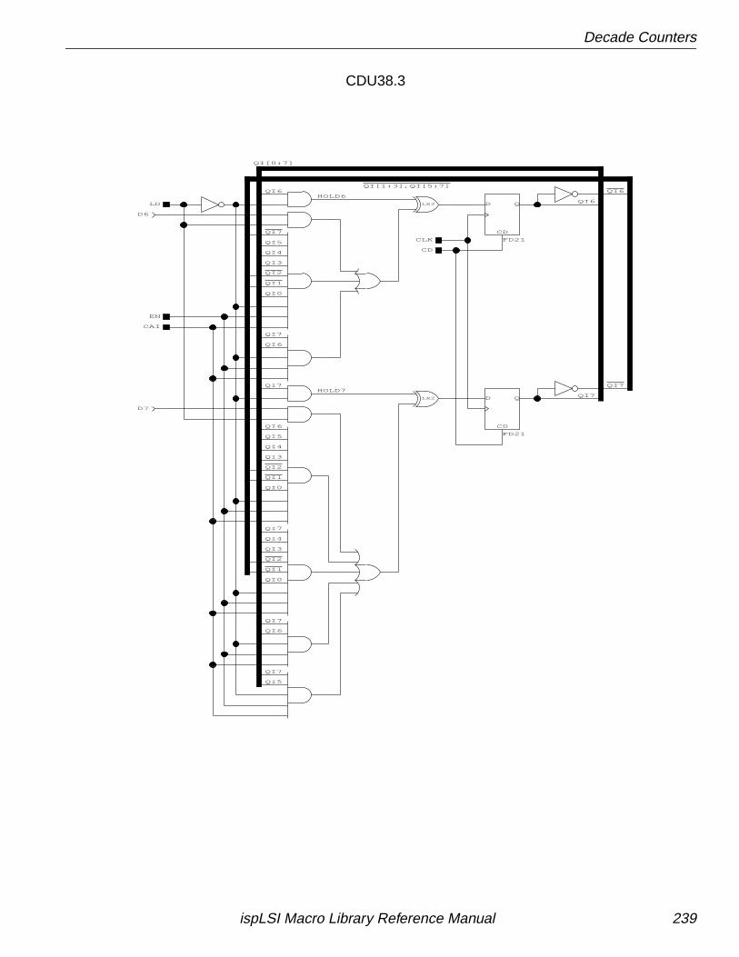
Decade Counters
QI6
QI1
QI2
QI7
QI7
QI1
QI2
QI1
QI2
QI[1:3],QI[5:7]
QI6
QI3
QI4
QI6
QI0
QI3
QI4
QI5
QI7
QI7
QI4
QI0
QI6
QI5
QI3
QI0
QI6
QI7
QI7
QI6
QI7
QI5
QI7
QI[0:7]
CAI
HOLD6
HOLD7
CD
QD
FD21
CD
QD
FD21
EN
LD
D7
D6
CD
CLK
LX2
LX2
CDU38.3
ispLSI Macro Library Reference Manual 239
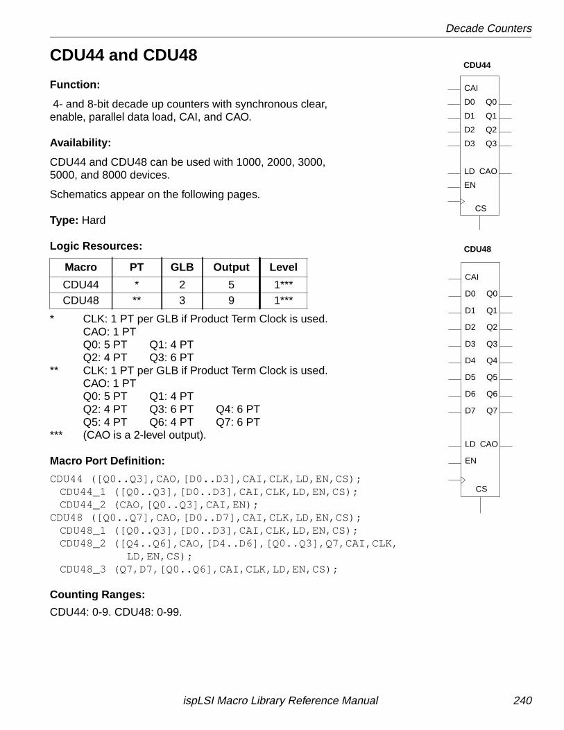
Decade Counters
CDU44 and CDU48
Function:
4- and 8-bit decade up counters with synchronous clear,enable, parallel data load, CAI, and CAO.
Availability:
CDU44 and CDU48 can be used with 1000, 2000, 3000,5000, and 8000 devices.
Schematics appear on the following pages.
Type: Hard
Logic Resources:
* CLK: 1 PT per GLB if Product Term Clock is used.CAO: 1 PTQ0: 5 PT Q1: 4 PTQ2: 4 PT Q3: 6 PT
** CLK: 1 PT per GLB if Product Term Clock is used.CAO: 1 PTQ0: 5 PT Q1: 4 PTQ2: 4 PT Q3: 6 PT Q4: 6 PTQ5: 4 PT Q6: 4 PT Q7: 6 PT
*** (CAO is a 2-level output).
Macro Port Definition:
CDU44 ([Q0..Q3],CAO,[D0..D3],CAI,CLK,LD,EN,CS);CDU44_1 ([Q0..Q3],[D0..D3],CAI,CLK,LD,EN,CS);CDU44_2 (CAO,[Q0..Q3],CAI,EN);
CDU48 ([Q0..Q7],CAO,[D0..D7],CAI,CLK,LD,EN,CS);CDU48_1 ([Q0..Q3],[D0..D3],CAI,CLK,LD,EN,CS);CDU48_2 ([Q4..Q6],CAO,[D4..D6],[Q0..Q3],Q7,CAI,CLK,
LD,EN,CS);CDU48_3 (Q7,D7,[Q0..Q6],CAI,CLK,LD,EN,CS);
Counting Ranges:
CDU44: 0-9. CDU48: 0-99.
Macro PT GLB Output Level
CDU44 * 2 5 1***CDU48 ** 3 9 1***
CDU44
CDU48
CS
CAI
Q0D0
Q1D1
Q2D2
Q3D3
EN
LD CAO
CS
CAI
Q0D0
Q1D1
Q2D2
Q3D3
Q4D4
Q5D5
Q6D6
EN
LD CAO
D7 Q7
ispLSI Macro Library Reference Manual 240
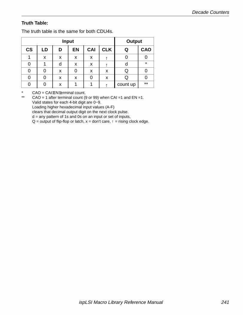
Decade Counters
Truth Table:
The truth table is the same for both CDU4s.
* CAO = CAI⋅EN⋅terminal count.** CAO = 1 after terminal count (9 or 99) when CAI =1 and EN =1.
Valid states for each 4-bit digit are 0~9.Loading higher hexadecimal input values (A-F)clears that decimal output digit on the next clock pulse.d = any pattern of 1s and 0s on an input or set of inputs,Q = output of flip-flop or latch, x = don’t care, ↑ = rising clock edge.
Input Output
CS LD D EN CAI CLK Q CAO
1 x x x x ↑ 0 00 1 d x x ↑ d *0 0 x 0 x x Q 00 0 x x 0 x Q 00 0 x 1 1 ↑ count up **
ispLSI Macro Library Reference Manual 241
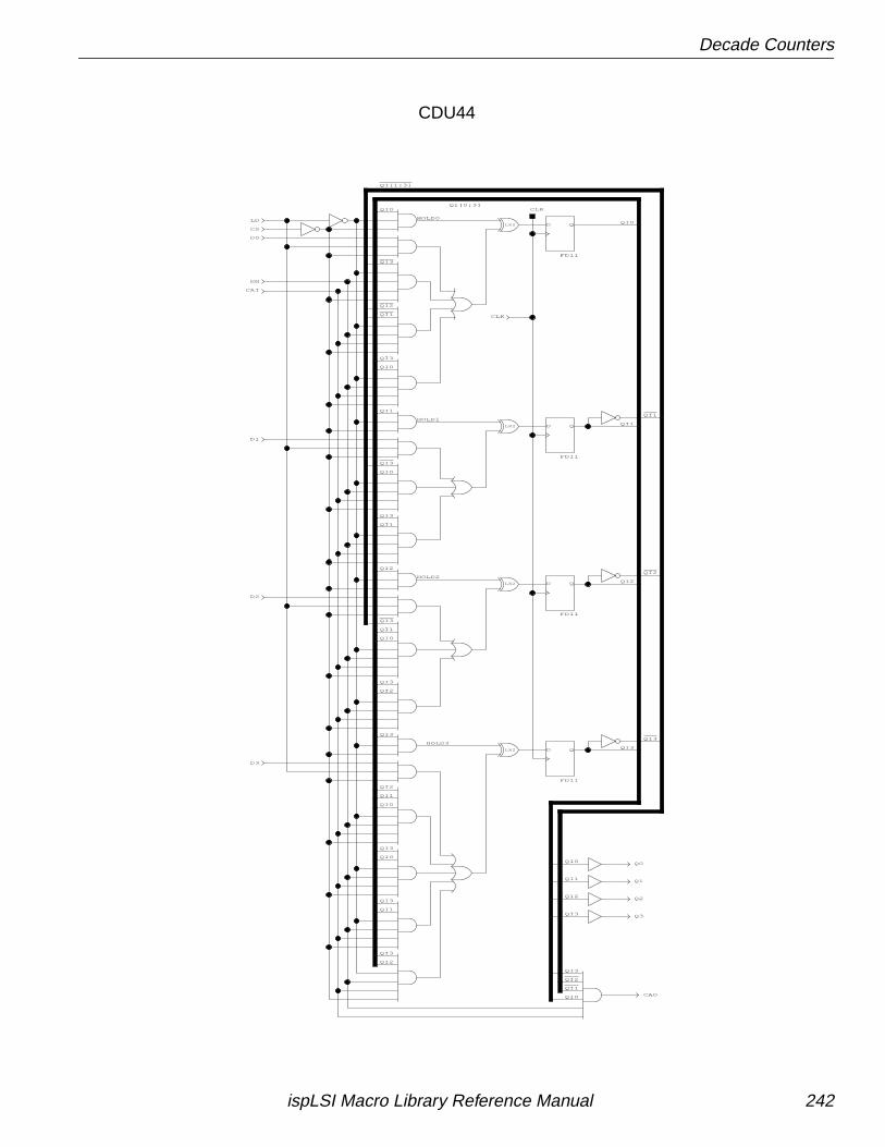
Decade Counters
QI3
QI1
QI0
QI[0:3]
QI3
QI0
QI1
QI0
QI3
QI1
QI2
QI1
QI0
QI3
QI2
QI1
QI3
QI0
QI3
QI3
QI2
QI3
QI0
QI1
QI2
QI0
QI1
QI2
QI3
QI0
QI0
QI2
QI3
QI1
QI1
QI3
QI2
QI1
QI3
QI3
QI[1:3]
QI2
QI2
QI3
Q3
Q2
Q1
Q0
CLK
CAO
D3
D2
D1
CLK
QD
FD11
QD
FD11
QD
FD11
HOLD0
HOLD3
QD
FD11
HOLD1
HOLD2
LD
CS
D0
EN
CAI
LX2
LX2
LX2
LX2
CDU44
ispLSI Macro Library Reference Manual 242
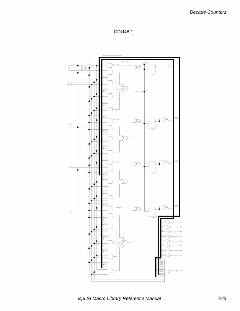
Decade Counters
QI3
QI2
QI[1:3],QI[5:7]
QI3
QI3
QI1
QI2
QI3
QI1
QI6
QI5
QI2
QI1
QI4
QI7
QI6
QI5
QI4
QI0
QI0
QI[0:7]
QI3
QI0
QI1
QI0
QI3
QI1
QI2
QI1
QI0
QI3
QI2
QI1
QI3
QI0
QI3
QI3
QI2
QI3
QI0
QI1
QI2
QI0
QI1
QI2
QI3
QI1
QI2
QI3
QI7
QI3
QI0
CAO
Q0
Q1
Q2
Q3
Q4
Q5
Q6
Q7
CAI
EN
D0
CS
LD
HOLD2
HOLD1
QD
FD11
HOLD3
HOLD0
QD
FD11
QD
FD11
QD
FD11
CLK
D1
D2
D3
CLK
LX2
LX2
LX2
LX2
CDU48.1
ispLSI Macro Library Reference Manual 243
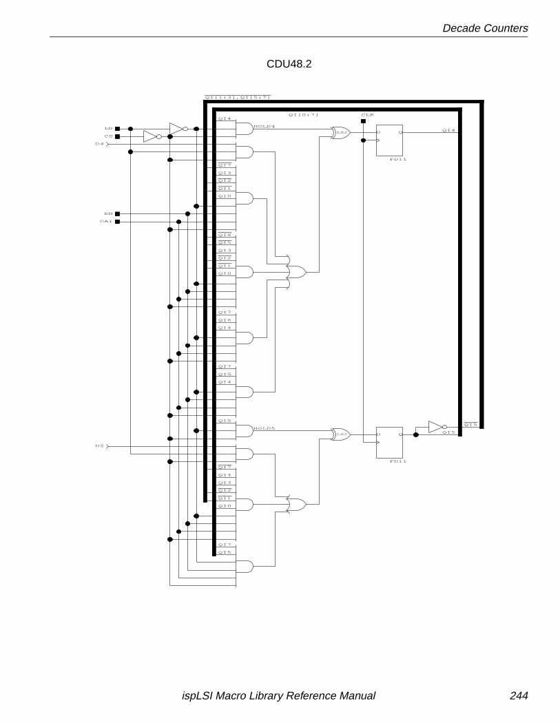
Decade Counters
QI4
QI3
QI0
QI5
QI7
QI0
QI3
QI4
QI5
QI4
QI5
QI7
QI4
QI6
QI7
QI0
QI3
QI4QI[0:7]
QI5
D5
D4
HOLD4
HOLD5
QD
FD11
QD
FD11
CLK
CS
LD
CAI
EN
LX2
LX2
QI7
QI2
QI1
QI1
QI2
QI7
QI1
QI2
QI5
QI6
QI[1:3],QI[5:7]
QI5
CDU48.2
ispLSI Macro Library Reference Manual 244
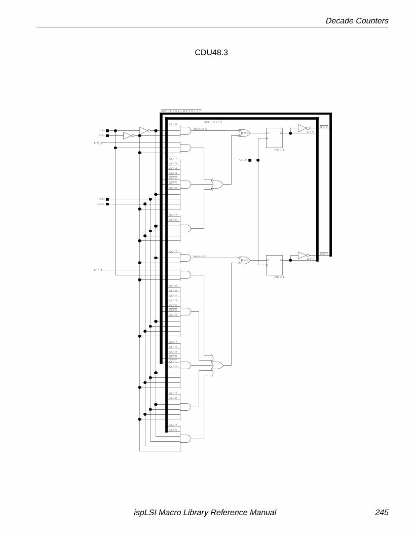
Decade Counters
QI6
QI[1:3],QI[5:7]
QI1
QI7
QI2
QI1
QI2
QI1
QI7
QI2
QI3
QI[0:7]
QI7
QI6
QI7
QI5
QI7
QI6
QI7
QI4
QI3
QI0
QI6
QI5
QI4
QI3
QI0
QI7
QI7
QI6
QI5
QI4
QI0
QI6
CLK
LD
EN
CAI
CS
QD
FD11
QD
FD11
HOLD7
HOLD6
D6
D7
LX2
LX2
CDU48.3
ispLSI Macro Library Reference Manual 245
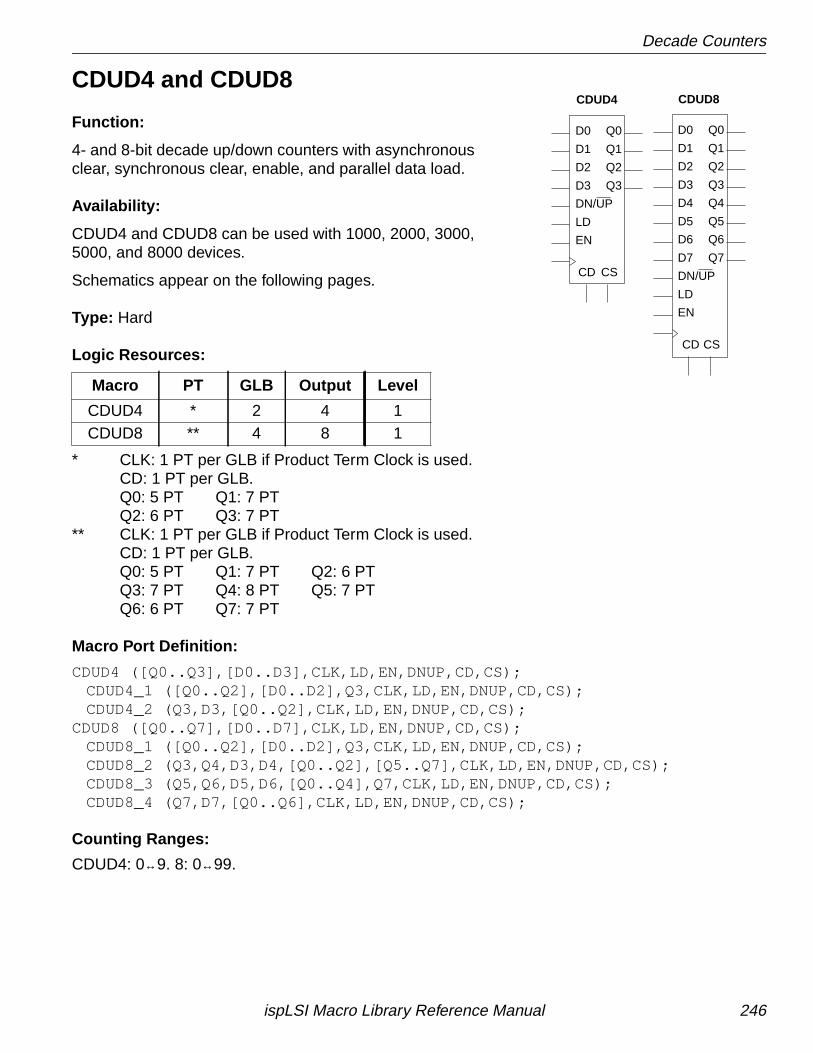
Decade Counters
CDUD4 and CDUD8
Function:
4- and 8-bit decade up/down counters with asynchronousclear, synchronous clear, enable, and parallel data load.
Availability:
CDUD4 and CDUD8 can be used with 1000, 2000, 3000,5000, and 8000 devices.
Schematics appear on the following pages.
Type: Hard
Logic Resources:
* CLK: 1 PT per GLB if Product Term Clock is used.CD: 1 PT per GLB.Q0: 5 PT Q1: 7 PTQ2: 6 PT Q3: 7 PT
** CLK: 1 PT per GLB if Product Term Clock is used.CD: 1 PT per GLB.Q0: 5 PT Q1: 7 PT Q2: 6 PTQ3: 7 PT Q4: 8 PT Q5: 7 PTQ6: 6 PT Q7: 7 PT
Macro Port Definition:
CDUD4 ([Q0..Q3],[D0..D3],CLK,LD,EN,DNUP,CD,CS);CDUD4_1 ([Q0..Q2],[D0..D2],Q3,CLK,LD,EN,DNUP,CD,CS);CDUD4_2 (Q3,D3,[Q0..Q2],CLK,LD,EN,DNUP,CD,CS);
CDUD8 ([Q0..Q7],[D0..D7],CLK,LD,EN,DNUP,CD,CS);CDUD8_1 ([Q0..Q2],[D0..D2],Q3,CLK,LD,EN,DNUP,CD,CS);CDUD8_2 (Q3,Q4,D3,D4,[Q0..Q2],[Q5..Q7],CLK,LD,EN,DNUP,CD,CS);CDUD8_3 (Q5,Q6,D5,D6,[Q0..Q4],Q7,CLK,LD,EN,DNUP,CD,CS);CDUD8_4 (Q7,D7,[Q0..Q6],CLK,LD,EN,DNUP,CD,CS);
Counting Ranges:
CDUD4: 0↔9. 8: 0↔99.
Macro PT GLB Output Level
CDUD4 * 2 4 1CDUD8 ** 4 8 1
CDUD4 CDUD8
DN/UP
Q0D0
Q1D1
Q2D2
Q3D3
CS
EN
LD
CD DN/UP
CD
Q7D7
LD
EN
CS
D6 Q6
D5 Q5
D4 Q4
D3 Q3
D2 Q2
D1 Q1
D0 Q0
ispLSI Macro Library Reference Manual 246
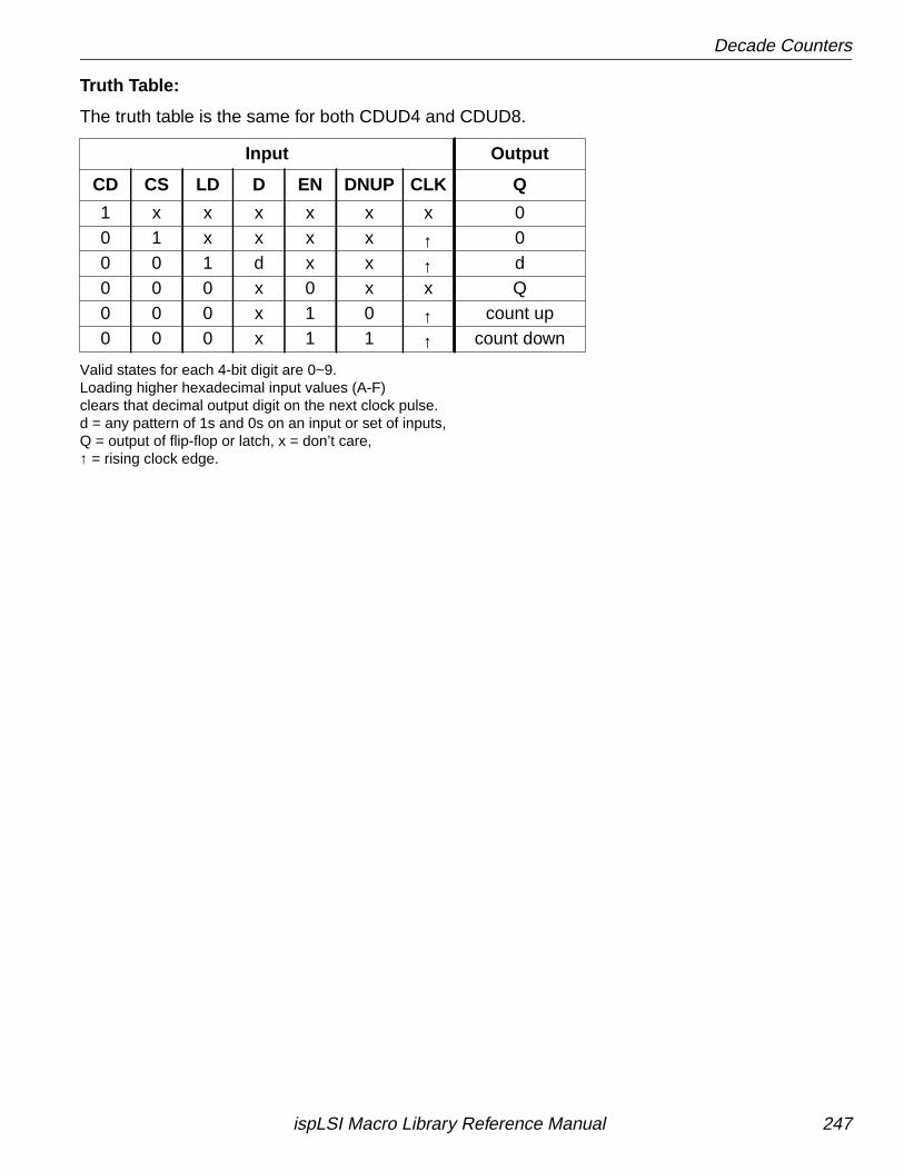
Decade Counters
Truth Table:
The truth table is the same for both CDUD4 and CDUD8.
Valid states for each 4-bit digit are 0~9.Loading higher hexadecimal input values (A-F)clears that decimal output digit on the next clock pulse.d = any pattern of 1s and 0s on an input or set of inputs,Q = output of flip-flop or latch, x = don’t care,↑ = rising clock edge.
Input Output
CD CS LD D EN DNUP CLK Q
1 x x x x x x 00 1 x x x x ↑ 00 0 1 d x x ↑ d0 0 0 x 0 x x Q0 0 0 x 1 0 ↑ count up0 0 0 x 1 1 ↑ count down
ispLSI Macro Library Reference Manual 247
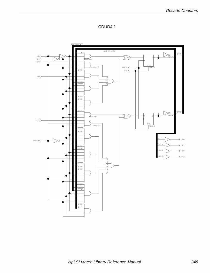
Decade Counters
QI0
QI1
QI2
QI3
QI[0:3]
QI3
QI1
QI0
QI1
QI3
QI3
QI1
QI2
QI0
QI0
QI0
QI1
Q0
Q1
Q2
Q3
QI1
QI[0:3]
QI0
QI3
QI0
QI3
QI2
QI0
QI2
QI1
QI3
QI0
LX2
LX2
CD
LOAD1CD
QD
FD21
LOAD0CD
QD
FD21
HOLD0
HOLD1
CS
LD
EN
DNUP
D0
D1
CLK
CDUD4.1
ispLSI Macro Library Reference Manual 248
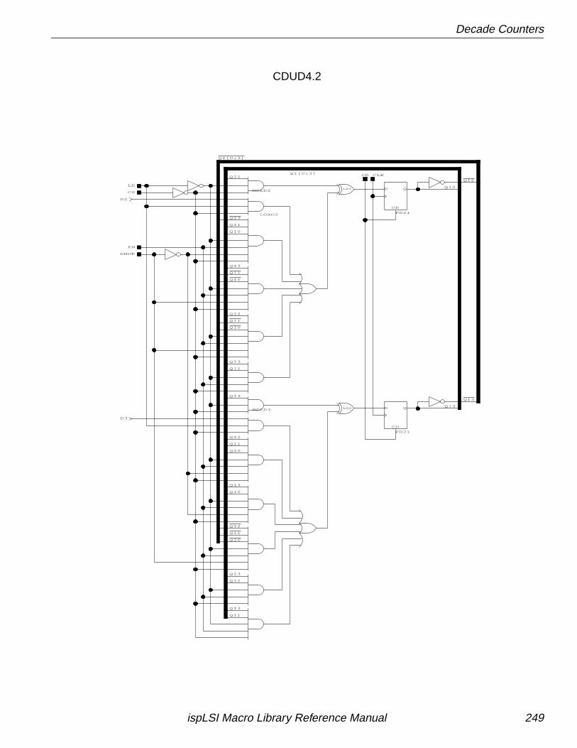
Decade Counters
QI[0:3]
QI1
QI0
QI3
QI0
QI1
QI0
QI1
QI2
QI3
QI2
QI2
QI[0:3]
QI0
QI3
QI2
QI3
QI3
QI2
QI3
QI0
QI2
QI1
QI2
QI1
QI0
QI3
QI2
QI3
QI1
QI3LX2
LX2
D3
D2
HOLD3
HOLD2
CD
QD
FD21
CLK
LOAD2
CD
QD
FD21
CD
CS
LD
DNUP
EN
CDUD4.2
ispLSI Macro Library Reference Manual 249
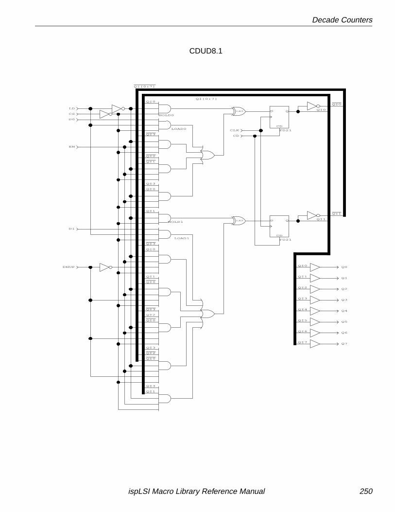
Decade Counters
QI1
QI2
QI3
QI4
QI3
QI1
QI0
QI1
QI3
QI3
QI1
QI2
QI0
QI0QI[0:7]
QI0
QI1
QI0
QI7
QI6
QI5
QI1
QI0
QI3
QI1
QI2
QI0
QI2
QI3
QI0
QI3
QI0
QI[0:7]
LX2
LX2
CLK
D1
D0
DNUP
EN
LD
CS
HOLD1
HOLD0
CD
QD
FD21LOAD0
CD
QD
FD21LOAD1
CD
Q0
Q1
Q2
Q3
Q4
Q5
Q6
Q7
CDUD8.1
ispLSI Macro Library Reference Manual 250
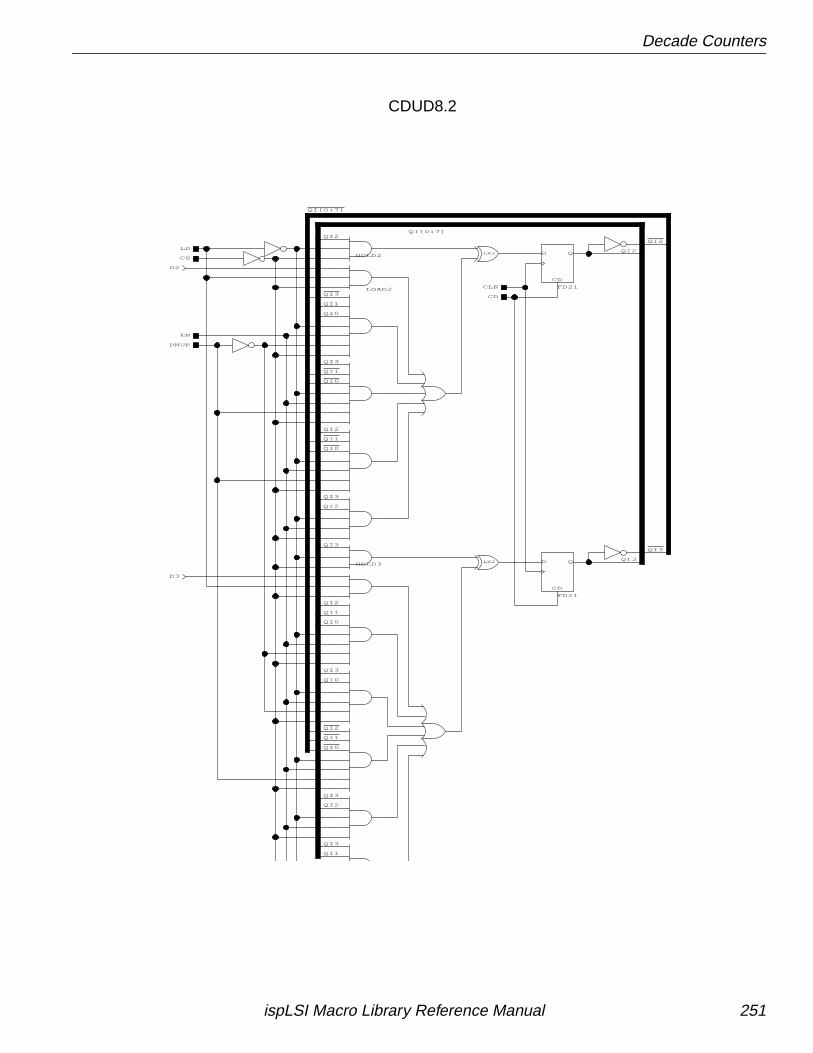
Decade Counters
QI2
QI3
QI1
QI3
QI2
QI3
QI0
QI1
QI2
QI1
QI2
QI0
QI3
QI2
QI3
QI3
QI2
QI3
QI0
QI[0:7]
LX2
LX2
CD
CLK
EN
DNUP
LD
CS
CD
QD
FD21LOAD2
CD
QD
FD21
HOLD2
HOLD3
QI2
QI3
QI2
QI1
QI0
QI1
QI0
QI3
QI0
QI1
QI[0:7]
D2
D3
CDUD8.2
ispLSI Macro Library Reference Manual 251
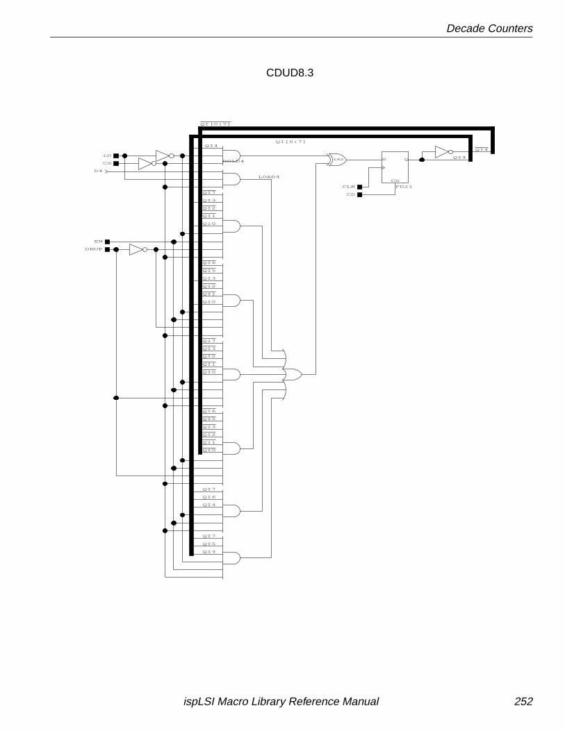
Decade Counters
QI[0:7]
QI2
QI3
QI5
QI6
QI0
QI1
QI2
QI3
QI7
QI1
QI2
QI5
QI6
QI0
QI1
QI7
QI2
QI1
QI4
LX2
CD
CLK
EN
DNUP
LD
CS
QI[0:7]
QI4
QI5
QI7
QI4
QI6
QI7
QI3
QI0
QI3
QI0
QI4
QI4
LOAD4CD
QD
FD21
HOLD4
D4
CDUD8.3
ispLSI Macro Library Reference Manual 252
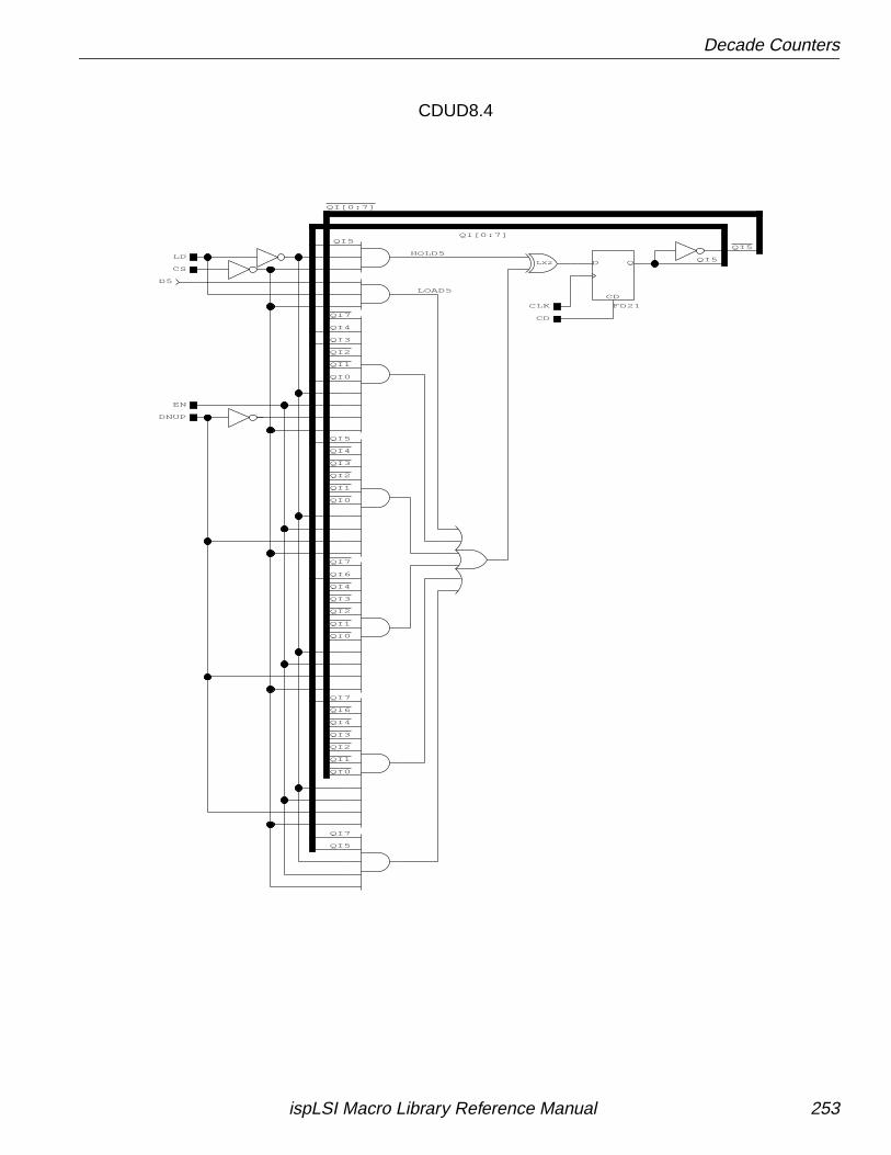
Decade Counters
QI[0:7]
QI5
QI7
QI7
QI6
QI5
QI5
QI4
QI3
QI0
QI5
LX2
QI5
QI[0:7]
QI1
QI2
QI3
QI4
QI6
QI0
QI7
QI4
QI3
QI1
QI2
QI0
QI7
QI2
QI1
QI4
QI3
QI2
QI1
QI0
CD
CLK
EN
DNUP
LD
LOAD5CD
QD
FD21
HOLD5
CS
D5
CDUD8.4
ispLSI Macro Library Reference Manual 253
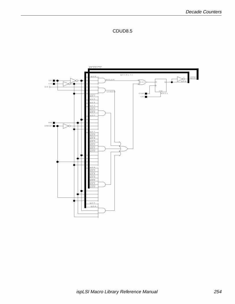
Decade Counters
QI[0:7]
QI6
QI7
QI6
QI7
QI0
QI3
QI4
QI5
QI6
QI6LX2
QI[0:7]
QI2
QI3
QI4
QI5
QI0
QI1
QI2
QI3
QI4
QI5
QI1
QI2
QI0
QI1
QI7
QI6
EN
DNUP
LD
LOAD6
CD
CLK
CD
QD
FD21
CS
HOLD6
D6
CDUD8.5
ispLSI Macro Library Reference Manual 254

Decade Counters
QI[0:7]
QI7
QI7
QI4
QI3
QI0
QI7
QI6
QI5
QI6
QI4
QI5
QI3
QI0
QI7
QI7
LX2
QI[0:7]
QI0
QI2
QI3
QI4
QI5
QI6
QI2
QI1
QI1
QI1
QI2
QI7
LD
EN
DNUP
CS
LOAD7
HOLD7
CLK
CD
CD
QD
FD21
D7
CDUD8.6
ispLSI Macro Library Reference Manual 255
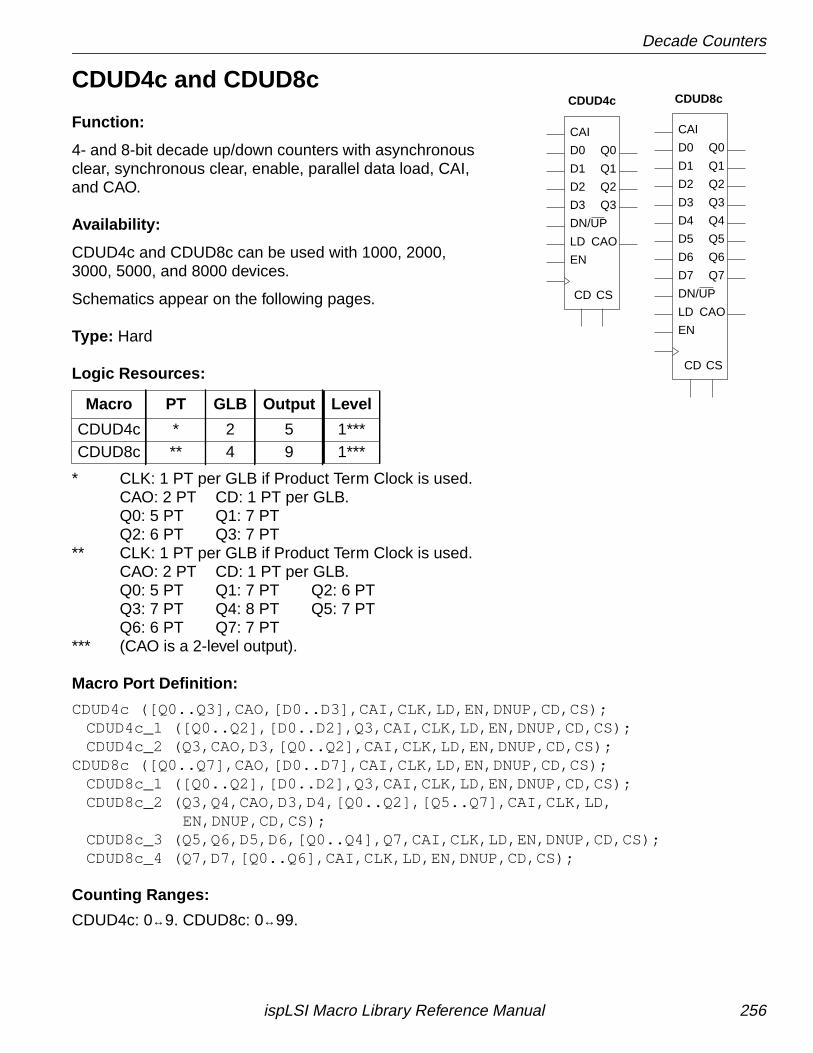
Decade Counters
CDUD4c and CDUD8c
Function:
4- and 8-bit decade up/down counters with asynchronousclear, synchronous clear, enable, parallel data load, CAI,and CAO.
Availability:
CDUD4c and CDUD8c can be used with 1000, 2000,3000, 5000, and 8000 devices.
Schematics appear on the following pages.
Type: Hard
Logic Resources:
* CLK: 1 PT per GLB if Product Term Clock is used.CAO: 2 PT CD: 1 PT per GLB.Q0: 5 PT Q1: 7 PTQ2: 6 PT Q3: 7 PT
** CLK: 1 PT per GLB if Product Term Clock is used.CAO: 2 PT CD: 1 PT per GLB.Q0: 5 PT Q1: 7 PT Q2: 6 PTQ3: 7 PT Q4: 8 PT Q5: 7 PTQ6: 6 PT Q7: 7 PT
*** (CAO is a 2-level output).
Macro Port Definition:
CDUD4c ([Q0..Q3],CAO,[D0..D3],CAI,CLK,LD,EN,DNUP,CD,CS);CDUD4c_1 ([Q0..Q2],[D0..D2],Q3,CAI,CLK,LD,EN,DNUP,CD,CS);CDUD4c_2 (Q3,CAO,D3,[Q0..Q2],CAI,CLK,LD,EN,DNUP,CD,CS);
CDUD8c ([Q0..Q7],CAO,[D0..D7],CAI,CLK,LD,EN,DNUP,CD,CS);CDUD8c_1 ([Q0..Q2],[D0..D2],Q3,CAI,CLK,LD,EN,DNUP,CD,CS);CDUD8c_2 (Q3,Q4,CAO,D3,D4,[Q0..Q2],[Q5..Q7],CAI,CLK,LD,
EN,DNUP,CD,CS);CDUD8c_3 (Q5,Q6,D5,D6,[Q0..Q4],Q7,CAI,CLK,LD,EN,DNUP,CD,CS);CDUD8c_4 (Q7,D7,[Q0..Q6],CAI,CLK,LD,EN,DNUP,CD,CS);
Counting Ranges:
CDUD4c: 0↔9. CDUD8c: 0↔99.
Macro PT GLB Output Level
CDUD4c * 2 5 1***CDUD8c ** 4 9 1***
CDUD4c CDUD8c
DN/UP
CAI
Q0D0
Q1D1
Q2D2
Q3D3
CS
EN
LD CAO
CD DN/UP
CD
Q7D7
CAOLD
EN
CS
D6 Q6
D5 Q5
D4 Q4
D3 Q3
D2 Q2
D1 Q1
D0 Q0
CAI
ispLSI Macro Library Reference Manual 256
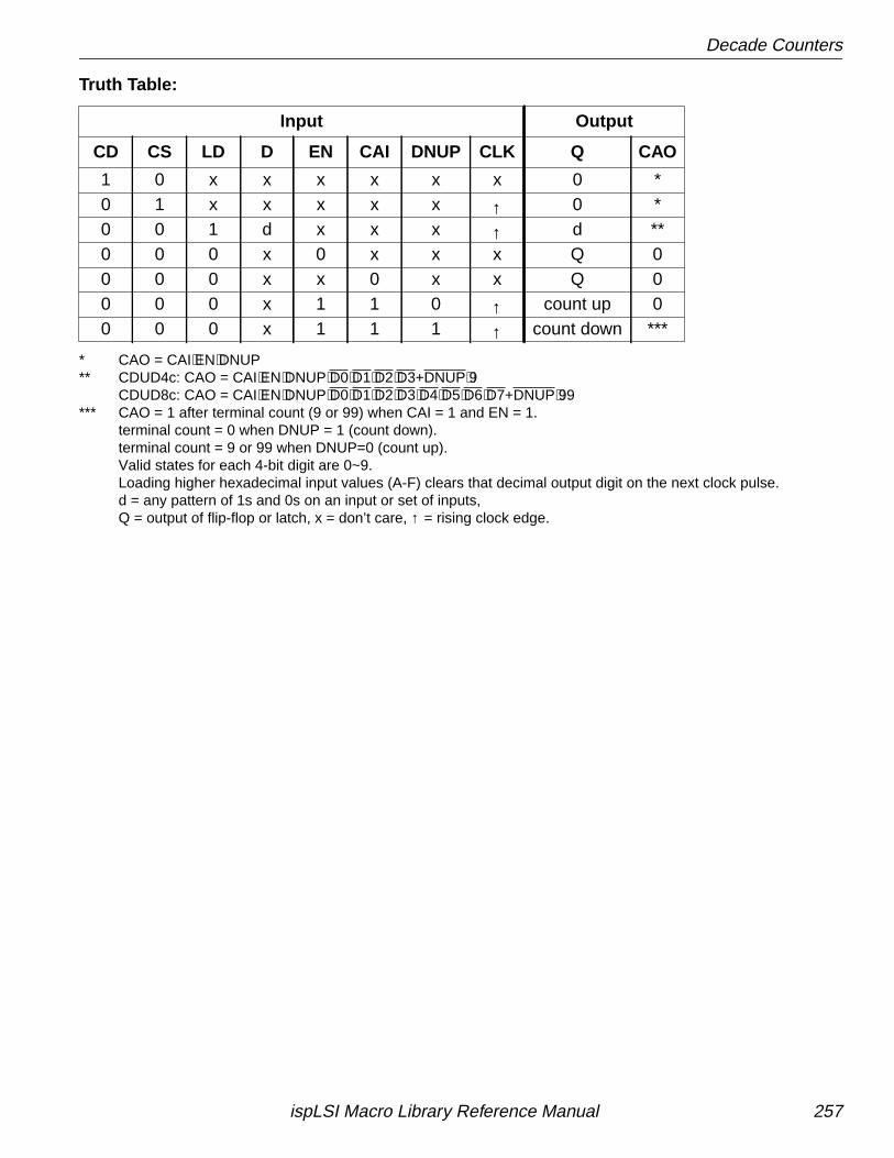
Decade Counters
Truth Table:
* CAO = CAI⋅EN⋅DNUP** CDUD4c: CAO = CAI⋅EN⋅DNUP⋅D0⋅D1⋅D2⋅D3+DNUP⋅9
CDUD8c: CAO = CAI⋅EN⋅DNUP⋅D0⋅D1⋅D2⋅D3⋅D4⋅D5⋅D6⋅D7+DNUP⋅99*** CAO = 1 after terminal count (9 or 99) when CAI = 1 and EN = 1.
terminal count = 0 when DNUP = 1 (count down).terminal count = 9 or 99 when DNUP=0 (count up).Valid states for each 4-bit digit are 0~9.Loading higher hexadecimal input values (A-F) clears that decimal output digit on the next clock pulse.d = any pattern of 1s and 0s on an input or set of inputs,Q = output of flip-flop or latch, x = don’t care, ↑ = rising clock edge.
Input Output
CD CS LD D EN CAI DNUP CLK Q CAO
1 0 x x x x x x 0 *0 1 x x x x x ↑ 0 *0 0 1 d x x x ↑ d **0 0 0 x 0 x x x Q 00 0 0 x x 0 x x Q 00 0 0 x 1 1 0 ↑ count up 00 0 0 x 1 1 1 ↑ count down ***
ispLSI Macro Library Reference Manual 257
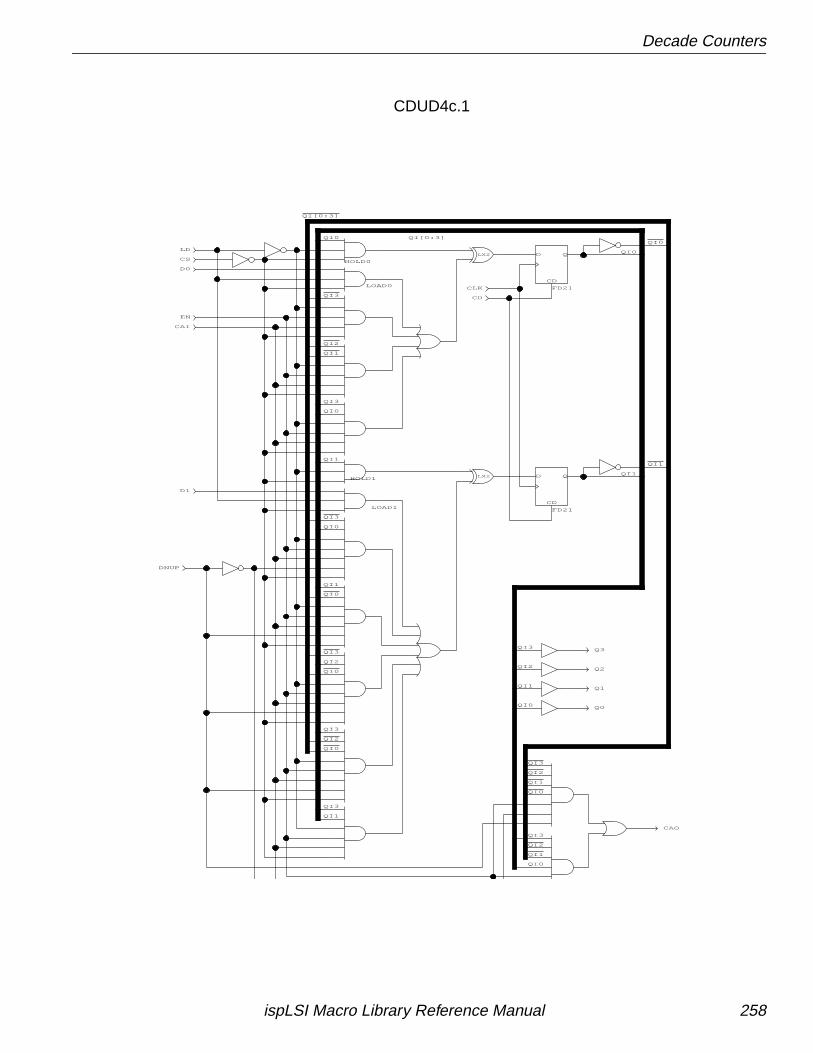
Decade Counters
Q3
Q2
Q0
Q1
QI0
QI2
QI3
QI1
QI0
QI1
QI0
QI1
QI0
QI3
QI0
QI3
QI1
QI3
QI2
QI1
QI[0:3]
QI0
QI3
QI0
QI1
QI2
QI3
QI2
QI1
QI0
QI3
QI1
QI2
QI0
QI0
QI3
QI2
QI0
QI3
QI1
QI[0:3]
CAO
LX2
LX2
CLK
EN
CS
LD
LOAD0CD
QD
FD21
CD
QD
FD21
HOLD0
HOLD1
LOAD1
DNUP
D0
CAI
D1
CD
CDUD4c.1
ispLSI Macro Library Reference Manual 258
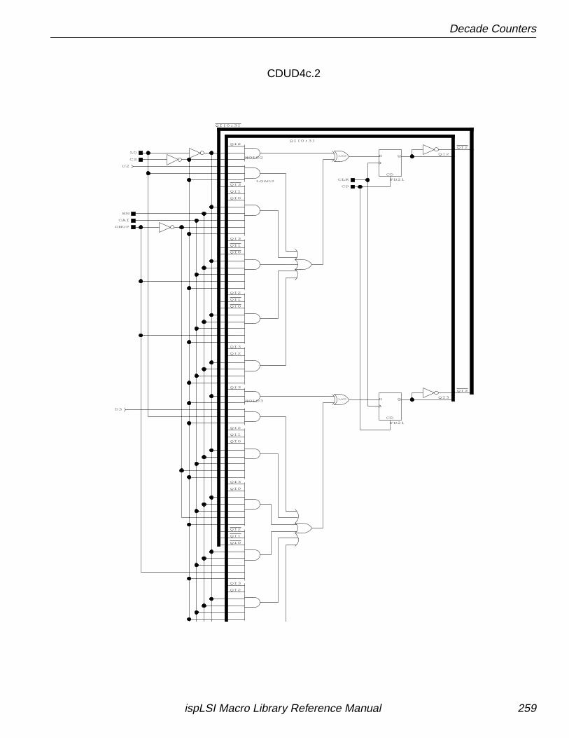
Decade Counters
QI[0:3]
QI3
QI0
QI1
QI0
QI1
QI3
QI2
QI0
QI1
QI2
LX2
LX2
CLK
CD
D2
EN
CAI
DNUP
LD
QI[0:3]
QI0
QI2
QI1
QI3
QI2
QI2
QI3
QI3
QI3
QI2
QI0
QI1
QI2
QI3
QI2
QI3
QI0
CD
QD
FD21
CS HOLD2
HOLD3
CD
QD
FD21
LOAD2
D3
CDUD4c.2
ispLSI Macro Library Reference Manual 259
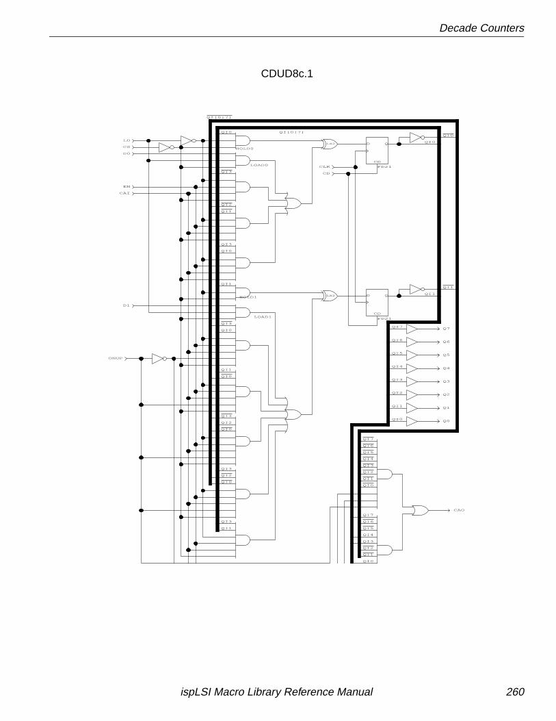
Decade Counters
Q7QI7
QI2
QI0
QI1
QI6
QI5
QI4
QI3
QI7
QI4
QI0
QI3
QI[0:7]
QI1
QI2
QI3
QI1
QI3
QI0
QI3
QI0
QI1
QI0
QI1
QI0
QI6
QI4
QI5
QI2
QI1
QI[0:7]
QI1
QI3
QI0
QI2
QI3
QI0
QI0
QI2
QI1
QI3
QI0
QI5
QI6
QI0
QI1
QI2
QI3
QI7
CAO
LX2
LX2
CD
D1
CAI
D0
DNUP
LOAD1
HOLD1
HOLD0
CD
QD
FD21
CD
QD
FD21LOAD0
LD
CS
EN
CLK
Q6
Q5
Q4
Q3
Q2
Q1
Q0
CDUD8c.1
ispLSI Macro Library Reference Manual 260
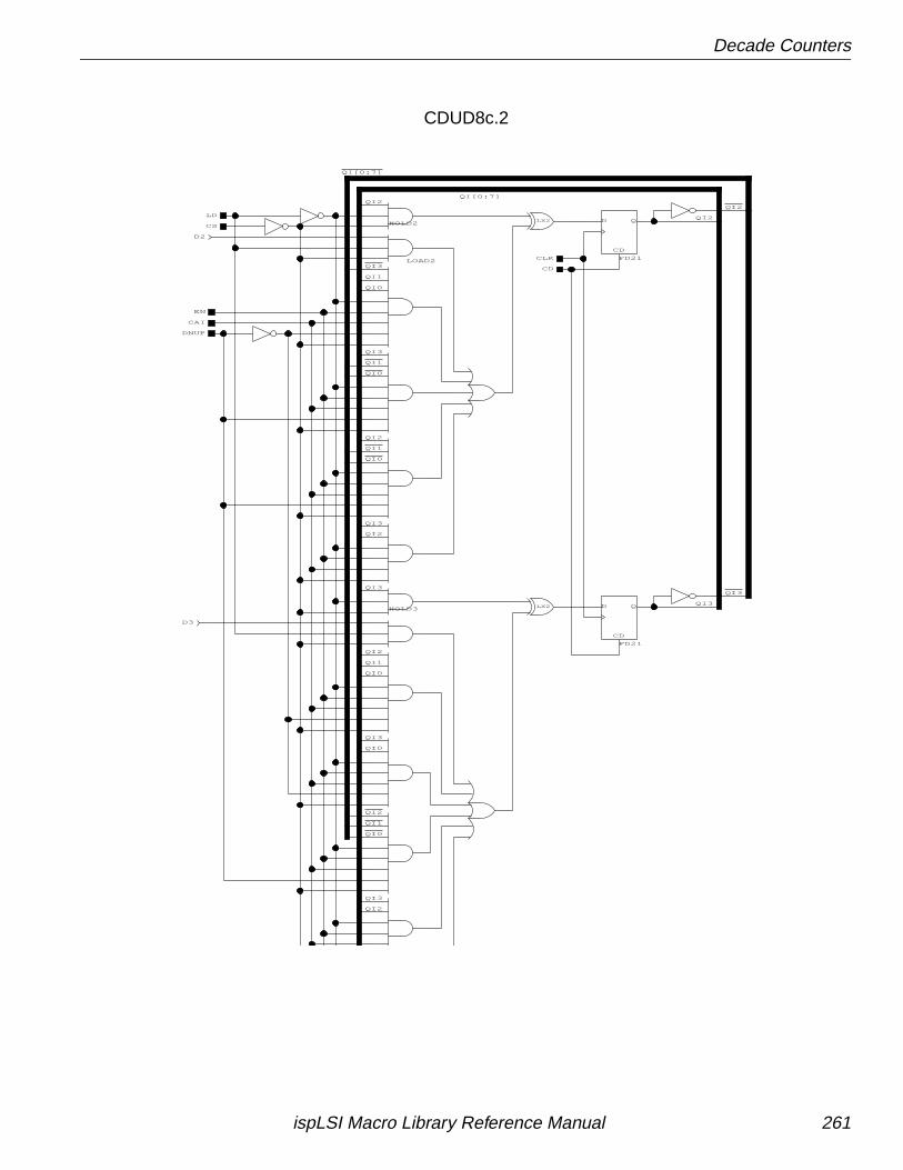
Decade Counters
QI2
QI1
QI0
QI2
QI3
QI1
QI0
QI1
QI0
QI3
QI[0:7]
LX2
LX2
D3
LOAD2
CD
QD
FD21
HOLD3
HOLD2CS
CD
QD
FD21
QI0
QI3
QI2
QI3
QI2
QI1
QI0
QI2
QI3
QI3
QI3
QI2
QI2
QI3
QI1
QI2
QI0
QI[0:7]
LD
DNUP
CAI
EN
D2
CD
CLK
CDUD8c.2
ispLSI Macro Library Reference Manual 261
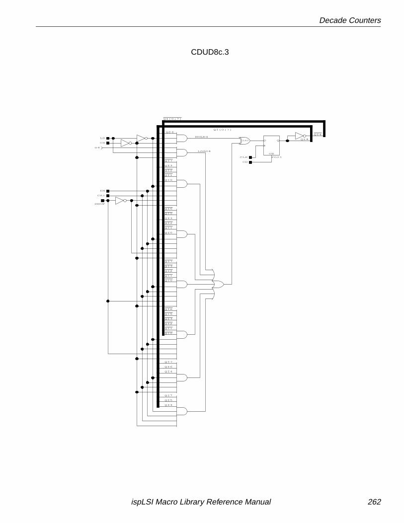
Decade Counters
QI6
QI5
QI3
QI2
QI1
QI0
QI7
QI3
QI2
QI1
QI0
QI6
QI5
QI2
QI1
QI1
QI2
QI7
QI4
QI[0:7]
QI7
QI5
QI4
QI7
QI6
QI4
QI3
QI0
QI0
QI3
QI4
QI4
QI[0:7]
LX2CS
LD
EN
CAI
DNUP
HOLD4
LOAD4
CLK
CD
CD
QD
FD21
D4
CDUD8c.3
ispLSI Macro Library Reference Manual 262
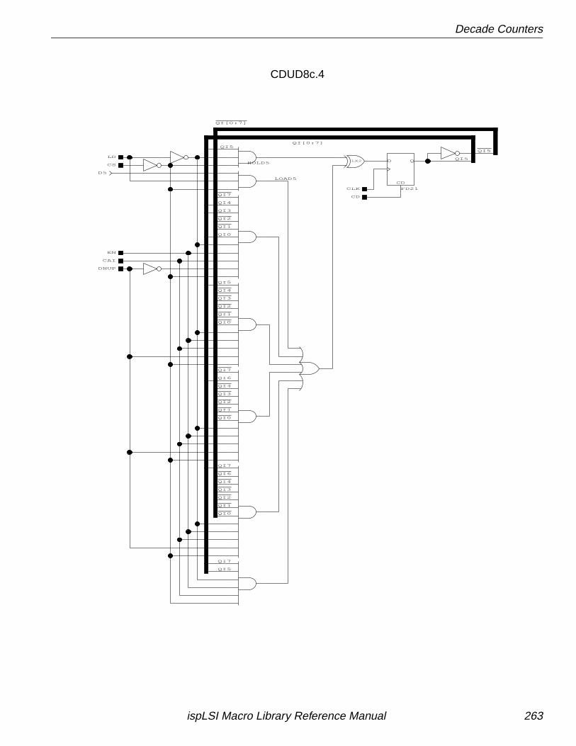
Decade Counters
QI[0:7]
QI5
QI6
QI4
QI3
QI2
QI1
QI0
QI7
QI4
QI3
QI2
QI1
QI0
QI7
QI2
QI1
QI0
QI1
QI2
QI4
QI3
LX2
QI[0:7]
QI5
QI7
QI5
QI7
QI6
QI5
QI4
QI3
QI0
QI5
EN
CAI
LD
DNUP
CD
CLK
LOAD5
HOLD5
CD
QD
FD21
CS
D5
CDUD8c.4
ispLSI Macro Library Reference Manual 263
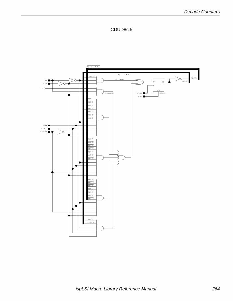
Decade Counters
QI[0:7]
QI6
QI1
QI2
QI7
QI0
QI1
QI2
QI3
QI4
QI5
QI0
QI1
QI2
QI3
QI4
QI5
LX2
EN
CAI
DNUP
LD
CD
CLK
QI[0:7]
QI6
QI0
QI3
QI4
QI5
QI6
QI7
QI6
QI7
QI6
LOAD6
HOLD6
CD
QD
FD21
CS
D6
CDUD8c.5
ispLSI Macro Library Reference Manual 264
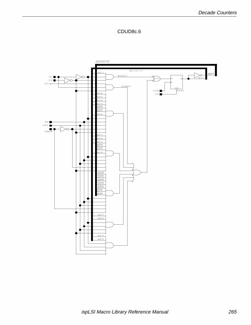
Decade Counters
QI[0:7]
QI7
QI2
QI1
QI2
QI1
QI0
QI1
QI2
QI3
QI6
QI4
QI5
LX2
CD
CLK
QI[0:7]
QI7
QI7
QI6
QI5
QI4
QI3
QI0
QI7
QI4
QI3
QI0
QI6
QI7
QI5
QI7
EN
CAI
DNUP
LD
CS
LOAD7CD
QD
FD21
HOLD7
D7
CDUD8c.6
ispLSI Macro Library Reference Manual 265
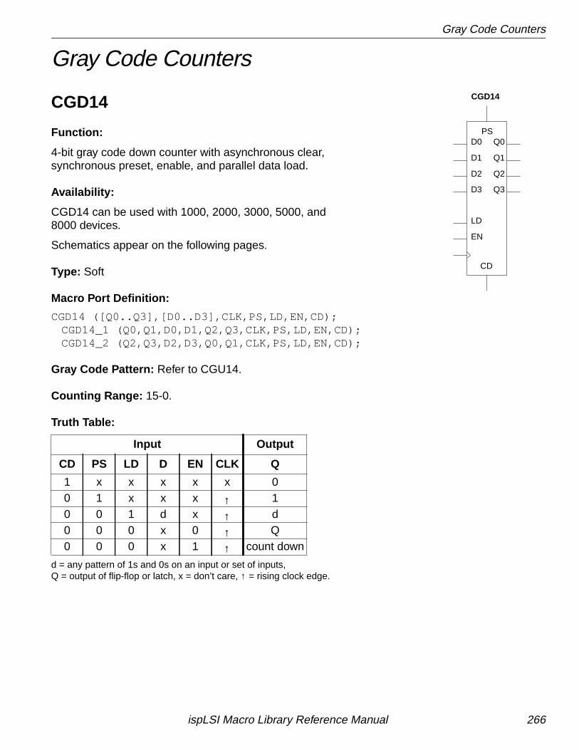
Gray Code Counters
Gray Code Counters
CGD14
Function:
4-bit gray code down counter with asynchronous clear,synchronous preset, enable, and parallel data load.
Availability:
CGD14 can be used with 1000, 2000, 3000, 5000, and8000 devices.
Schematics appear on the following pages.
Type: Soft
Macro Port Definition:
CGD14 ([Q0..Q3],[D0..D3],CLK,PS,LD,EN,CD);CGD14_1 (Q0,Q1,D0,D1,Q2,Q3,CLK,PS,LD,EN,CD);CGD14_2 (Q2,Q3,D2,D3,Q0,Q1,CLK,PS,LD,EN,CD);
Gray Code Pattern: Refer to CGU14.
Counting Range: 15-0.
Truth Table:
d = any pattern of 1s and 0s on an input or set of inputs,Q = output of flip-flop or latch, x = don’t care, ↑ = rising clock edge.
Input Output
CD PS LD D EN CLK Q
1 x x x x x 00 1 x x x ↑ 10 0 1 d x ↑ d0 0 0 x 0 ↑ Q0 0 0 x 1 ↑ count down
CD
Q0D0
Q1D1
Q2D2
Q3D3
EN
LD
PS
CGD14
ispLSI Macro Library Reference Manual 266
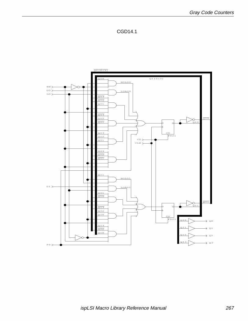
Gray Code Counters
QI3
QI2
QI1
QI0
QI1
QI0
QI3
QI0
QI1
QI1
QI3
QI2
QI3
QI2
QI0
QI1
QI[0:3]QI0
QI1
QI2
CD
QD
FD21
QI2
QI3
QI1
QI1
QI2
QI0
QI1
QI[0:3]
QI3
QI3
QI2
QI0
HOLD0
LOAD0
LOAD1
HOLD1
CD
QD
FD21
LD
D0
EN
D1
PS
CD
CLK
Q3
Q2
Q1
Q0
CGD14.1
ispLSI Macro Library Reference Manual 267
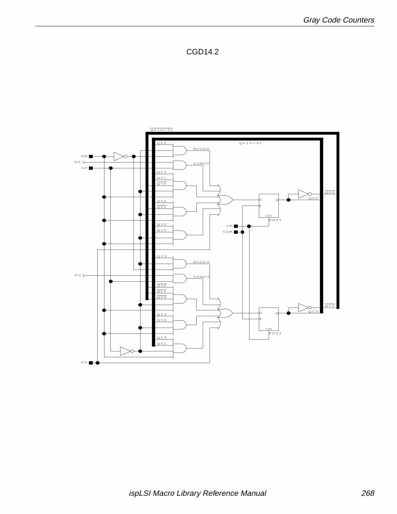
Gray Code Counters
QI[0:3]
QI2
QI0
QI1
QI1
QI0
QI3
QI2
CLK
HOLD3
CD
PS
LD
EN
CD
QD
FD21
CD
QD
FD21
D3
D2
LOAD3
LOAD2
HOLD2
QI[0:3]
QI2
QI3
QI2
QI2
QI2
QI0
QI3
QI3
QI0
QI3
QI1
QI1
QI3
CGD14.2
ispLSI Macro Library Reference Manual 268

Gray Code Counters
CGD24
Function:
4-bit gray code down counter with synchronous clear,synchronous preset, enable, and parallel data load.
Availability:
CGD24 can be used with 1000, 2000, 3000, 5000, and8000 devices.
Schematics appear on the following pages.
Type: Soft
Macro Port Definition:
CGD24 ([Q0..Q3],[D0..D3],CLK,PS,LD,EN,CS);CGD24_1 (Q0,Q1,D0,D1,Q2,Q3,CLK,PS,LD,EN,CS);CGD24_2 (Q2,Q3,D2,D3,Q0,Q1,CLK,PS,LD,EN,CS);
Gray Code Pattern: Refer to CGU14.
Counting Range: 15-0.
Truth Table:
d = any pattern of 1s and 0s on an input or set of inputs,Q = output of flip-flop or latch, x = don’t care,↑ = rising clock edge.
Input Output
PS CS LD D EN CLK Q
1 x x x x ↑ 10 1 x x x ↑ 00 0 1 d x ↑ d0 0 0 x 0 ↑ Q0 0 0 x 1 ↑ count down
CS
Q0D0
Q1D1
Q2D2
Q3D3
EN
LD
PS
CGD24
ispLSI Macro Library Reference Manual 269
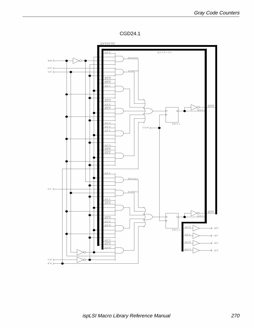
Gray Code Counters
Q0
Q1
Q2
Q3
QI2
QI1
QI0
QI3
QI0
QI2
QI3
QI2
QI3
QI1
QI1
QI0
QI3
QI0
QI[0:3]
QI1
QI0
QI1
QI1
QI2
QI1
QI1QI0
QI1
QI[0:3]
QI3
QI2
QI3
QI2
QI0
QI3
QI2
QD
FD11
LOAD0LD
D0
EN
HOLD1
D1
LOAD1
PS
QD
FD11
CS
HOLD0
CLK
CGD24.1
ispLSI Macro Library Reference Manual 270
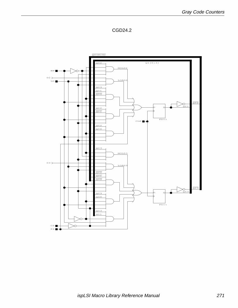
Gray Code Counters
QI[0:3]
QI0
QI1
QI1
QI0
QI3
QI2
QI2
QD
FD11
HOLD3
LOAD3
LD
D3
EN
QD
FD11
HOLD2
D2
LOAD2
PS
CS
CLK
QI1
QI1
QI3
QI0
QI3
QI3
QI0
QI2
QI2
QI2 QI[0:3]
QI2
QI3
QI3
CGD24.2
ispLSI Macro Library Reference Manual 271
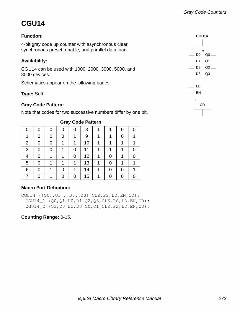
Gray Code Counters
CGU14
Function:
4-bit gray code up counter with asynchronous clear,synchronous preset, enable, and parallel data load.
Availability:
CGU14 can be used with 1000, 2000, 3000, 5000, and8000 devices.
Schematics appear on the following pages.
Type: Soft
Gray Code Pattern:
Note that codes for two successive numbers differ by one bit.
Macro Port Definition:
CGU14 ([Q0..Q3],[D0..D3],CLK,PS,LD,EN,CD);CGU14_1 (Q0,Q1,D0,D1,Q2,Q3,CLK,PS,LD,EN,CD);CGU14_2 (Q2,Q3,D2,D3,Q0,Q1,CLK,PS,LD,EN,CD);
Counting Range: 0-15.
Gray Code Pattern
0 0 0 0 0 8 1 1 0 01 0 0 0 1 9 1 1 0 12 0 0 1 1 10 1 1 1 13 0 0 1 0 11 1 1 1 04 0 1 1 0 12 1 0 1 05 0 1 1 1 13 1 0 1 16 0 1 0 1 14 1 0 0 17 0 1 0 0 15 1 0 0 0
CD
Q0D0
Q1D1
Q2D2
Q3D3
EN
LD
PS
CGU14
ispLSI Macro Library Reference Manual 272
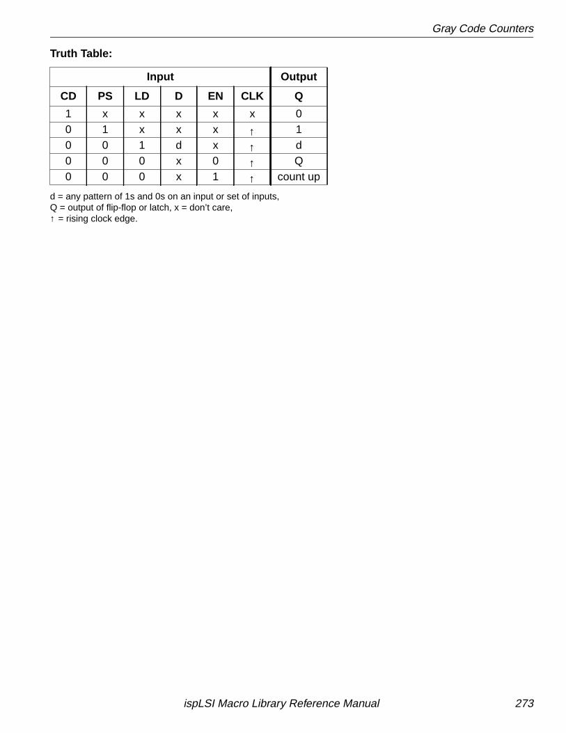
Gray Code Counters
Truth Table:
d = any pattern of 1s and 0s on an input or set of inputs,Q = output of flip-flop or latch, x = don’t care,↑ = rising clock edge.
Input Output
CD PS LD D EN CLK Q
1 x x x x x 00 1 x x x ↑ 10 0 1 d x ↑ d0 0 0 x 0 ↑ Q0 0 0 x 1 ↑ count up
ispLSI Macro Library Reference Manual 273
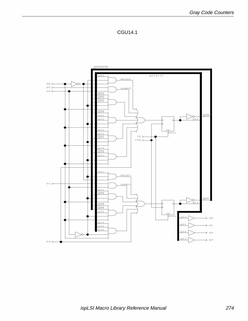
Gray Code Counters
QI1
QI2
QI3
QI0
QI0
QI2
QI3
QI0
QI1
QI1
QI1
QI3
QI2
QI3
QI1
QI2
QI0
QI1
QI[0:3]QI0
Q0
Q1
Q2
Q3
QI3
QI0
QI2
QI1
QI3
QI1
QI2
QI0
QI1
QI[0:3]
QI3
QI2
HOLD0
LOAD0
LOAD1
HOLD1
CD
QD
FD21
CD
QD
FD21
LD
D0
EN
D1
PS
CD
CLK
CGU14.1
ispLSI Macro Library Reference Manual 274
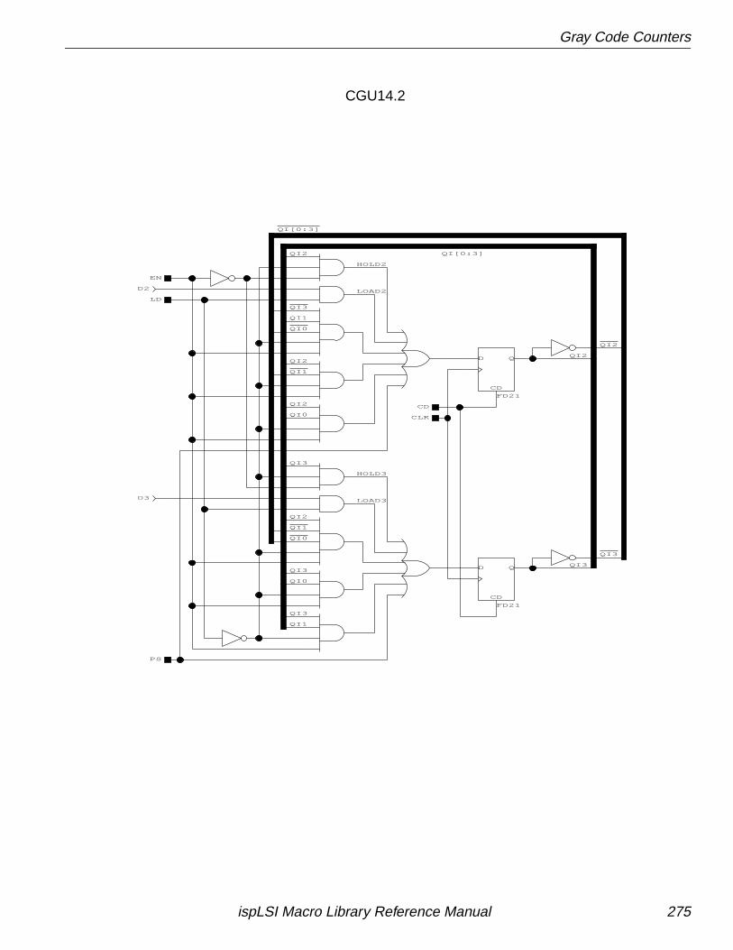
Gray Code Counters
QI[0:3]
QI2
QI0
QI1
QI1
QI0
QI3
QI3
CLK
HOLD3
CD
PS
LD
EN
QI[0:3]
QI2
QI3
QI2
QI2
QI2
QI0
QI3
QI2
QI3
QI0
QI3
QI1
QI1
CD
QD
FD21
CD
QD
FD21
D3
D2
LOAD3
LOAD2
HOLD2
CGU14.2
ispLSI Macro Library Reference Manual 275
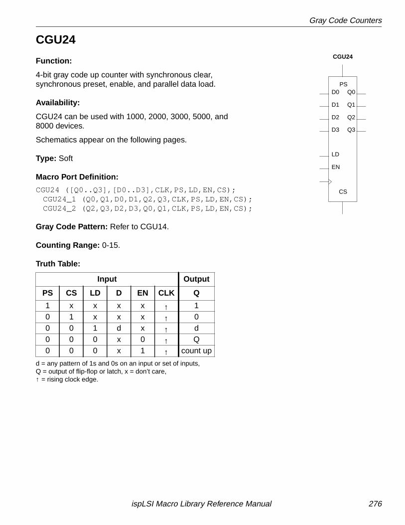
Gray Code Counters
CGU24
Function:
4-bit gray code up counter with synchronous clear,synchronous preset, enable, and parallel data load.
Availability:
CGU24 can be used with 1000, 2000, 3000, 5000, and8000 devices.
Schematics appear on the following pages.
Type: Soft
Macro Port Definition:
CGU24 ([Q0..Q3],[D0..D3],CLK,PS,LD,EN,CS);CGU24_1 (Q0,Q1,D0,D1,Q2,Q3,CLK,PS,LD,EN,CS);CGU24_2 (Q2,Q3,D2,D3,Q0,Q1,CLK,PS,LD,EN,CS);
Gray Code Pattern: Refer to CGU14.
Counting Range: 0-15.
Truth Table:
d = any pattern of 1s and 0s on an input or set of inputs,Q = output of flip-flop or latch, x = don’t care,↑ = rising clock edge.
Input Output
PS CS LD D EN CLK Q
1 x x x x ↑ 10 1 x x x ↑ 00 0 1 d x ↑ d0 0 0 x 0 ↑ Q0 0 0 x 1 ↑ count up
CS
Q0D0
Q1D1
Q2D2
Q3D3
EN
LD
PS
CGU24
ispLSI Macro Library Reference Manual 276
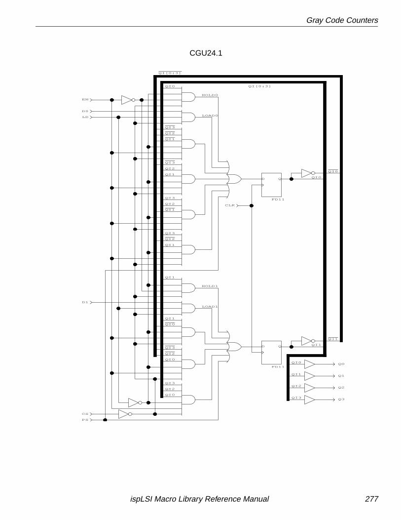
Gray Code Counters
QI2
QI1
QI0
QI0
QI1
QI[0:3]
QI0
QI2
QI3
QI0
QI1
QI1
QI1
QI3
QI2
QI3
QI1
QI2
QI0
QI3
Q0
Q1
Q2
Q3
QI1
QI3
QI2
QI0
QI2
QI1
QI3
QI2
QI1
QI[0:3]
QI3
QI0
CLK
HOLD0
CS
QD
FD11
PS
LOAD1
D1
HOLD1
EN
D0
LD LOAD0
QD
FD11
CGU24.1
ispLSI Macro Library Reference Manual 277
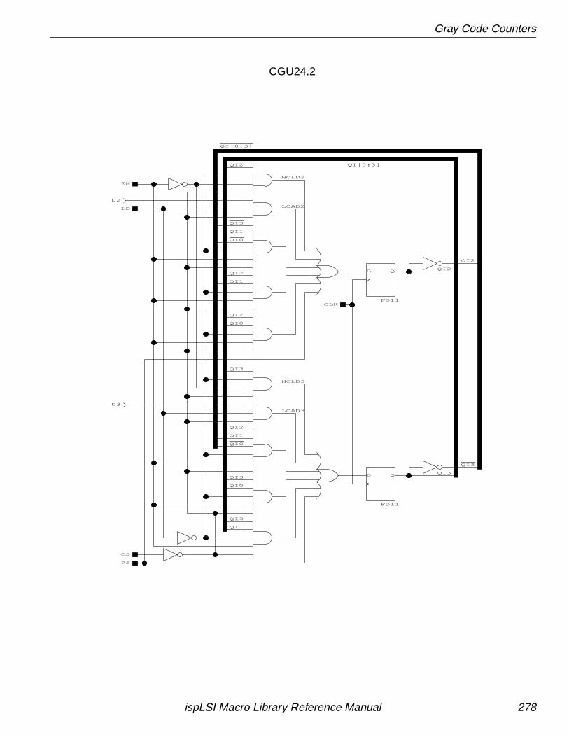
Gray Code Counters
QI2
QI3
QI0
QI3
QI1
QI1
QI0
QI[0:3]
CLK
CS
PS
QI3
QI2
QI[0:3]QI2
QI2
QI2
QI0
QI3
QI2
QI3
QI0
QI3
QI1
QI1
LOAD2
D2
HOLD2
QD
FD11
EN
D3
LD
LOAD3
HOLD3
QD
FD11
CGU24.2
ispLSI Macro Library Reference Manual 278
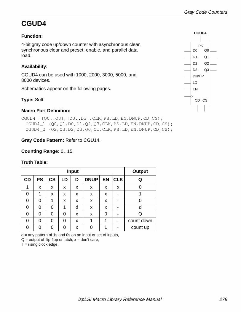
Gray Code Counters
CGUD4
Function:
4-bit gray code up/down counter with asynchronous clear,synchronous clear and preset, enable, and parallel dataload.
Availability:
CGUD4 can be used with 1000, 2000, 3000, 5000, and8000 devices.
Schematics appear on the following pages.
Type: Soft
Macro Port Definition:
CGUD4 ([Q0..Q3],[D0..D3],CLK,PS,LD,EN,DNUP,CD,CS);CGUD4_1 (Q0,Q1,D0,D1,Q2,Q3,CLK,PS,LD,EN,DNUP,CD,CS);CGUD4_2 (Q2,Q3,D2,D3,Q0,Q1,CLK,PS,LD,EN,DNUP,CD,CS);
Gray Code Pattern: Refer to CGU14.
Counting Range: 0↔15.
Truth Table:
d = any pattern of 1s and 0s on an input or set of inputs,Q = output of flip-flop or latch, x = don’t care,↑ = rising clock edge.
Input Output
CD PS CS LD D DNUP EN CLK Q
1 x x x x x x x 00 1 x x x x x ↑ 10 0 1 x x x x ↑ 00 0 0 1 d x x ↑ d0 0 0 0 x x 0 ↑ Q0 0 0 0 x 1 1 ↑ count down0 0 0 0 x 0 1 ↑ count up
DN/UP
PSQ0D0
Q1D1
Q2D2
Q3D3
CS
EN
LD
CD
CGUD4
ispLSI Macro Library Reference Manual 279
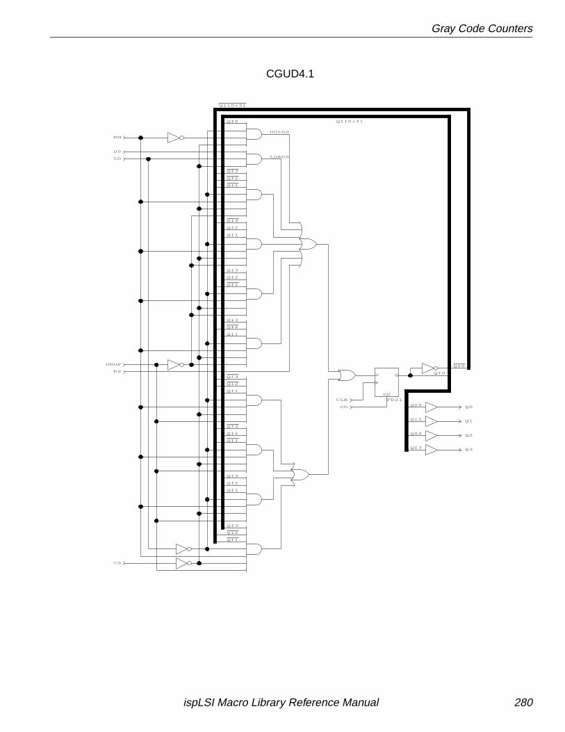
Gray Code Counters
QI0
QI1
QI2
QI3
QI[0:3]QI0
QI1
QI3
QI2
QI3
QI1
QI2
QI3
QI2
QI1
QI3
QI0
QI1
QI2
Q3
Q2
Q1
Q0
QI[0:3]
QI3
QI1
QI2
QI1
QI2
QI3
QI2
QI3
QI1
QI3
QI1
QI2
QI0
CD
CD
QD
FD21
PS
EN
D0
LD LOAD0
CS
DNUP
HOLD0
CLK
CGUD4.1
ispLSI Macro Library Reference Manual 280
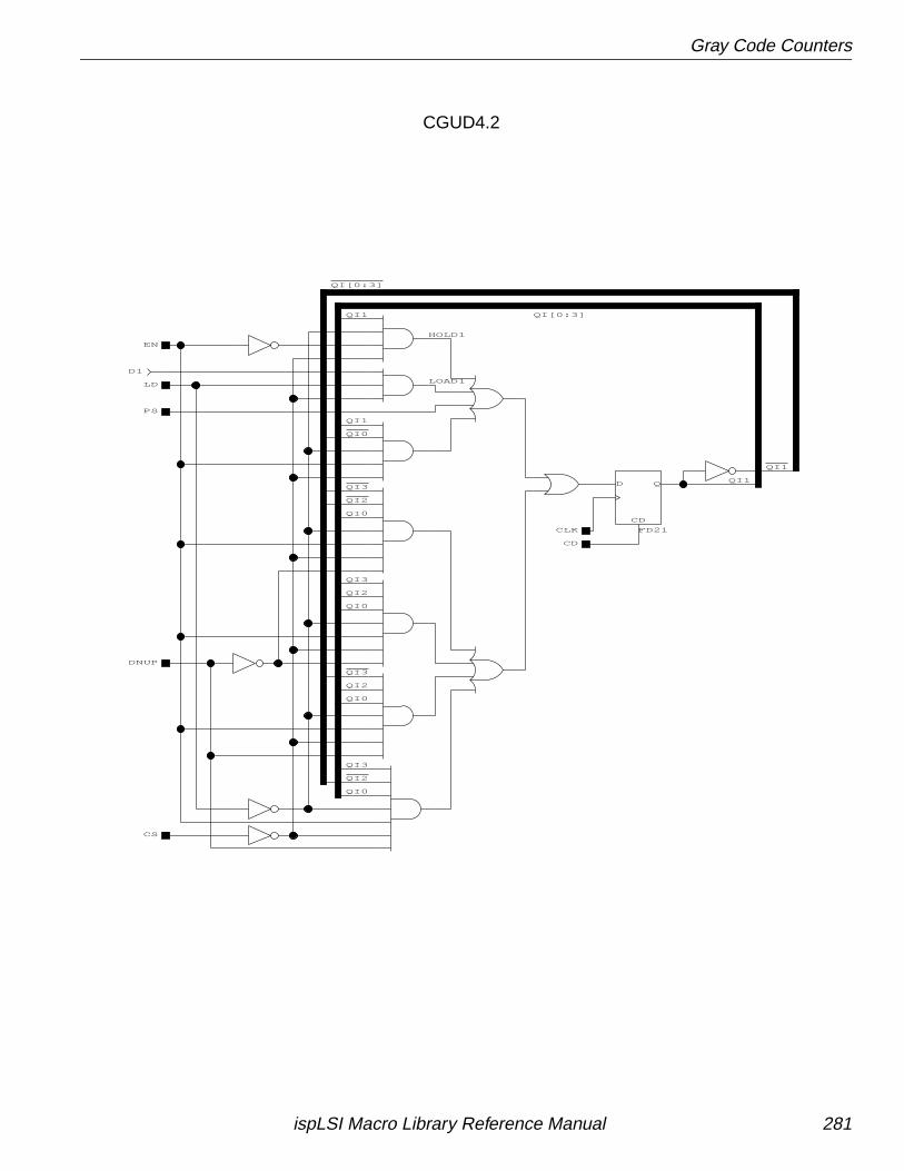
Gray Code Counters
QI0
QI3
QI2
QI0
QI1
QI1
QI0
QI2
QI0
QI3
QI1
QI[0:3]
CD
QD
FD21
D1
LOAD1
HOLD1
QI2
QI3
QI[0:3]
QI0
QI3
QI2
QI1
DNUP
CS
PS
LD
EN
CD
CLK
CGUD4.2
ispLSI Macro Library Reference Manual 281
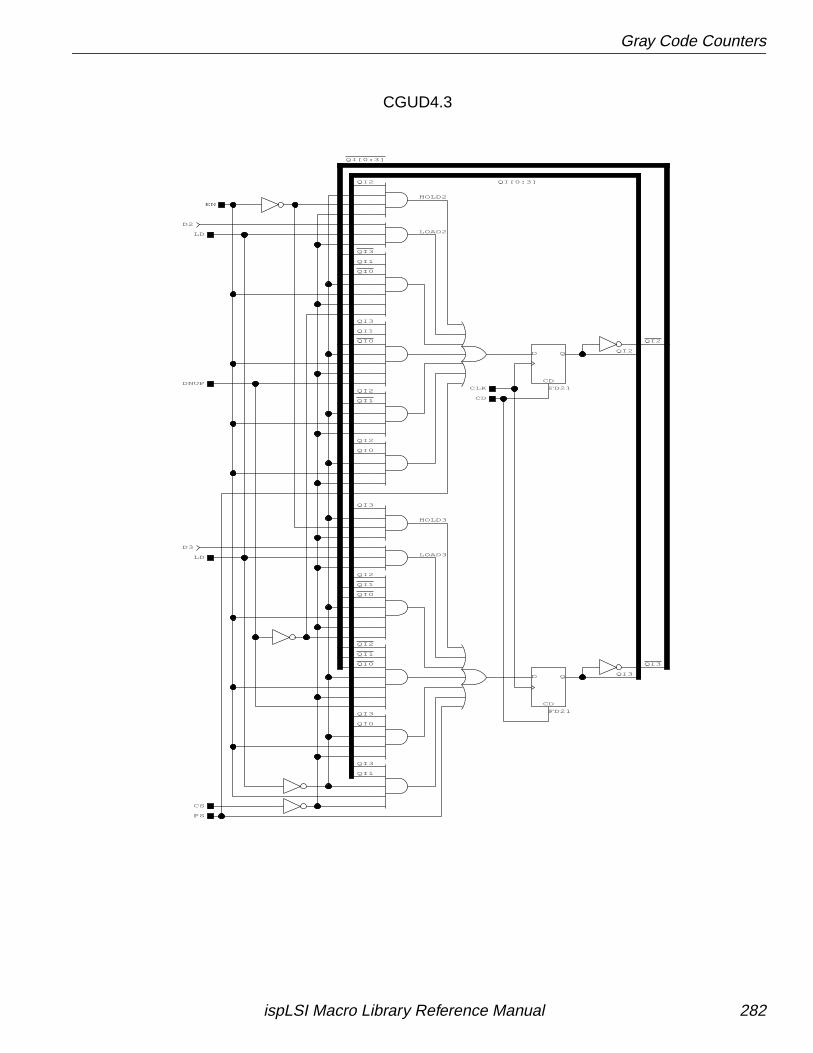
Gray Code Counters
QI1
QI0
QI2
QI1
QI0
QI0
QI3
QI2
QI[0:3]
QI1
QI0
QI3
CD
QD
FD21
CD
QD
FD21
LOAD2
HOLD2
HOLD3
LOAD3
QI1
QI3
QI3
QI3
QI3
QI2
QI2
QI3
QI1
QI2
QI0
QI2
QI1
QI[0:3]
QI2
QI0
EN
D2
D3
LD
LD
CS
PS
DNUPCLK
CD
CGUD4.3
ispLSI Macro Library Reference Manual 282
I/O Pins
This chapter contains information on the following macros:
■ Bidirectional Pins
■ Input Pins
■ Output Pins
ispLSI Macro Library Reference Manual 283
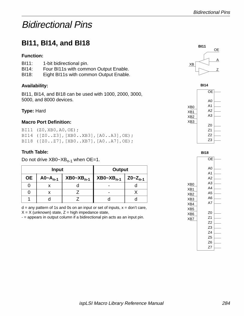
Bidirectional Pins
Bidirectional Pins
BI11, BI14, and BI18
Function:
BI11: 1-bit bidirectional pin.BI14: Four BI11s with common Output Enable.BI18: Eight BI11s with common Output Enable.
Availability:
BI11, BI14, and BI18 can be used with 1000, 2000, 3000,5000, and 8000 devices.
Type: Hard
Macro Port Definition:
BI11 (Z0,XB0,A0,OE);BI14 ([Z0..Z3],[XB0..XB3],[A0..A3],OE);BI18 ([Z0..Z7],[XB0..XB7],[A0..A7],OE);
Truth Table:
Do not drive XB0~XBn-1 when OE=1.
d = any pattern of 1s and 0s on an input or set of inputs, x = don’t care,X = X (unknown) state, Z = high impedance state,- = appears in output column if a bidirectional pin acts as an input pin.
Input Output
OE A0~An-1 XB0~XBn-1 XB0~XBn-1 Z0~Zn-1
0 x d - d0 x Z - X1 d Z d d
BI11
BI14
BI18
A
Z
XB
OE
XB0XB1XB2
Z0Z1Z2
OE
A0
A3A2A1
Z3
XB3
Z6
XB3XB2XB1XB0
Z2Z1Z0
A5
A7XB4XB5XB6
Z5
OE
A0
A3A2A1
Z7
XB7
A4
A6
Z3Z4
ispLSI Macro Library Reference Manual 284
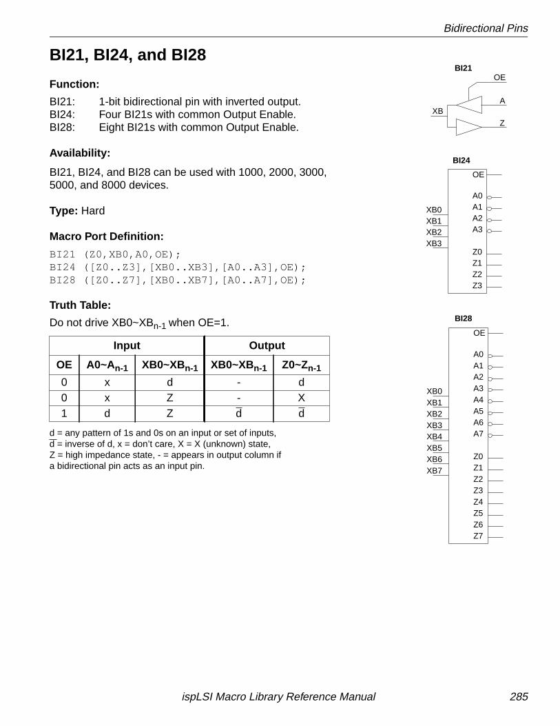
Bidirectional Pins
BI21, BI24, and BI28
Function:
BI21: 1-bit bidirectional pin with inverted output.BI24: Four BI21s with common Output Enable.BI28: Eight BI21s with common Output Enable.
Availability:
BI21, BI24, and BI28 can be used with 1000, 2000, 3000,5000, and 8000 devices.
Type: Hard
Macro Port Definition:
BI21 (Z0,XB0,A0,OE);BI24 ([Z0..Z3],[XB0..XB3],[A0..A3],OE);BI28 ([Z0..Z7],[XB0..XB7],[A0..A7],OE);
Truth Table:
Do not drive XB0~XBn-1 when OE=1.
d = any pattern of 1s and 0s on an input or set of inputs,d = inverse of d, x = don’t care, X = X (unknown) state,Z = high impedance state, - = appears in output column ifa bidirectional pin acts as an input pin.
Input Output
OE A0~An-1 XB0~XBn-1 XB0~XBn-1 Z0~Zn-1
0 x d - d0 x Z - X1 d Z d d
BI21
BI24
BI28
A
Z
XB
OE
XB0XB1XB2
Z0Z1Z2
OE
A0
A3A2A1
Z3
XB3
Z6
XB3XB2XB1XB0
Z2Z1Z0
A5
A7XB4XB5XB6
Z5
OE
A0
A3A2A1
Z7
XB7
A4
A6
Z3Z4
ispLSI Macro Library Reference Manual 285
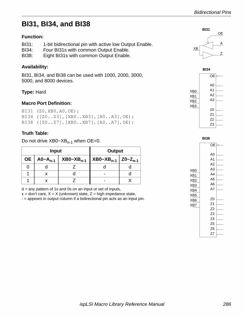
Bidirectional Pins
BI31, BI34, and BI38
Function:
BI31: 1-bit bidirectional pin with active low Output Enable.BI34: Four BI31s with common Output Enable.BI38: Eight BI31s with common Output Enable.
Availability:
BI31, BI34, and BI38 can be used with 1000, 2000, 3000,5000, and 8000 devices.
Type: Hard
Macro Port Definition:
BI31 (Z0,XB0,A0,OE);BI34 ([Z0..Z3],[XB0..XB3],[A0..A3],OE);BI38 ([Z0..Z7],[XB0..XB7],[A0..A7],OE);
Truth Table:
Do not drive XB0~XBn-1 when OE=0.
d = any pattern of 1s and 0s on an input or set of inputs,x = don’t care, X = X (unknown) state, Z = high impedance state,- = appears in output column if a bidirectional pin acts as an input pin.
Input Output
OE A0~An-1 XB0~XBn-1 XB0~XBn-1 Z0~Zn-1
0 d Z d d1 x d - d1 x Z - X
BI31
BI34
BI38
A
ZXB
OE
XB0XB1XB2
Z0Z1Z2
OE
A0
A3A2A1
Z3
XB3
Z6
XB3XB2XB1XB0
Z2Z1Z0
A5
A7XB4XB5XB6
Z5
OE
A0
A3A2A1
Z7
XB7
A4
A6
Z3Z4
ispLSI Macro Library Reference Manual 286
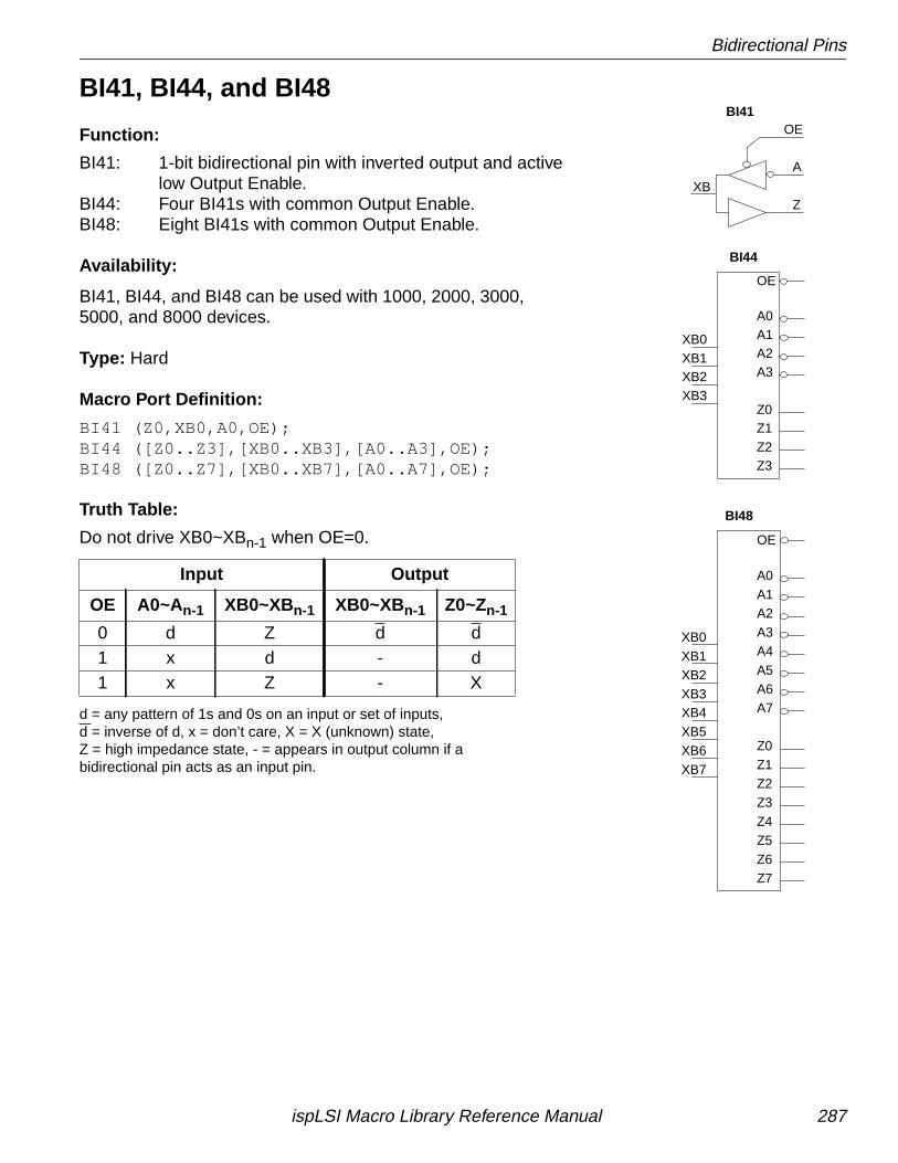
Bidirectional Pins
BI41, BI44, and BI48
Function:
BI41: 1-bit bidirectional pin with inverted output and activelow Output Enable.
BI44: Four BI41s with common Output Enable.BI48: Eight BI41s with common Output Enable.
Availability:
BI41, BI44, and BI48 can be used with 1000, 2000, 3000,5000, and 8000 devices.
Type: Hard
Macro Port Definition:
BI41 (Z0,XB0,A0,OE);BI44 ([Z0..Z3],[XB0..XB3],[A0..A3],OE);BI48 ([Z0..Z7],[XB0..XB7],[A0..A7],OE);
Truth Table:
Do not drive XB0~XBn-1 when OE=0.
d = any pattern of 1s and 0s on an input or set of inputs,d = inverse of d, x = don’t care, X = X (unknown) state,Z = high impedance state, - = appears in output column if abidirectional pin acts as an input pin.
Input Output
OE A0~An-1 XB0~XBn-1 XB0~XBn-1 Z0~Zn-1
0 d Z d d1 x d - d1 x Z - X
BI41
BI44
BI48
A
ZXB
OE
XB0XB1XB2
Z0Z1Z2
OE
A0
A3A2A1
Z3
XB3
Z6
XB3XB2XB1XB0
Z2Z1Z0
A5
A7XB4XB5XB6
Z5
OE
A0
A3A2A1
Z7
XB7
A4
A6
Z3Z4
ispLSI Macro Library Reference Manual 287
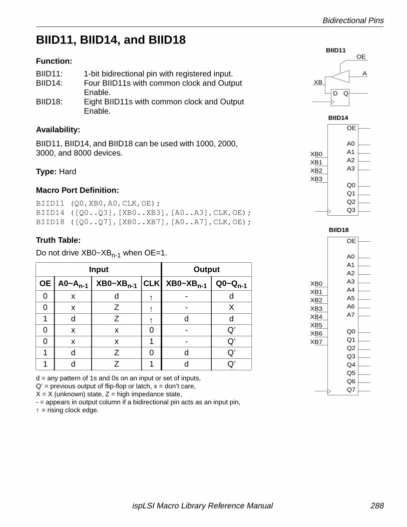
Bidirectional Pins
BIID11, BIID14, and BIID18
Function:
BIID11: 1-bit bidirectional pin with registered input.BIID14: Four BIID11s with common clock and Output
Enable.BIID18: Eight BIID11s with common clock and Output
Enable.
Availability:
BIID11, BIID14, and BIID18 can be used with 1000, 2000,3000, and 8000 devices.
Type: Hard
Macro Port Definition:
BIID11 (Q0,XB0,A0,CLK,OE);BIID14 ([Q0..Q3],[XB0..XB3],[A0..A3],CLK,OE);BIID18 ([Q0..Q7],[XB0..XB7],[A0..A7],CLK,OE);
Truth Table:
Do not drive XB0~XBn-1 when OE=1.
d = any pattern of 1s and 0s on an input or set of inputs,Q’ = previous output of flip-flop or latch, x = don’t care,X = X (unknown) state, Z = high impedance state,- = appears in output column if a bidirectional pin acts as an input pin,↑ = rising clock edge.
Input Output
OE A0~An-1 XB0~XBn-1 CLK XB0~XB n-1 Q0~Qn-1
0 x d ↑ - d0 x Z ↑ - X1 d Z ↑ d d0 x x 0 - Q’0 x x 1 - Q’1 d Z 0 d Q’1 d Z 1 d Q’
BIID11
BIID14
BIID18
D
A
Q
XB
OE
XB3
Q3
Q1Q0
XB0XB1
A3A2A1
OE
A0
Q2
XB2
OE
A0
XB2XB1XB0
XB3
Q2
Q0Q1
Q3
A4
A6
Q7
Q5Q4
XB4XB5
A3A2A1
Q6
XB6XB7
A5
A7
ispLSI Macro Library Reference Manual 288
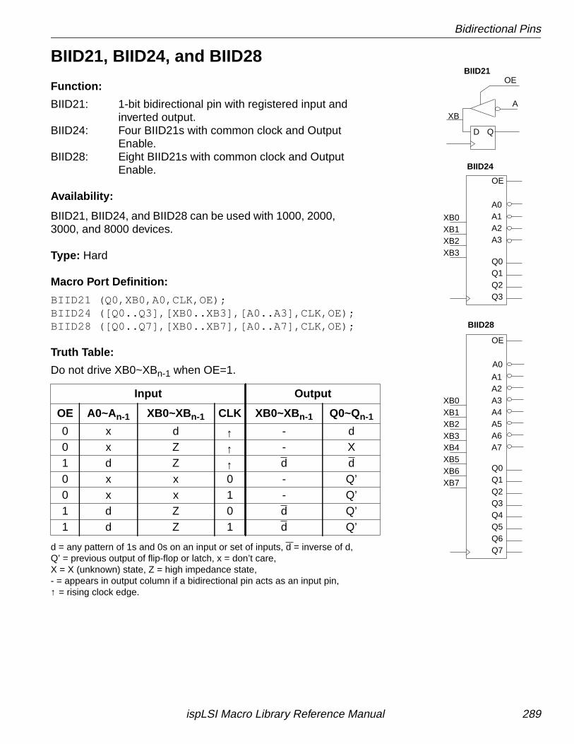
Bidirectional Pins
BIID21, BIID24, and BIID28
Function:
BIID21: 1-bit bidirectional pin with registered input andinverted output.
BIID24: Four BIID21s with common clock and OutputEnable.
BIID28: Eight BIID21s with common clock and OutputEnable.
Availability:
BIID21, BIID24, and BIID28 can be used with 1000, 2000,3000, and 8000 devices.
Type: Hard
Macro Port Definition:
BIID21 (Q0,XB0,A0,CLK,OE);BIID24 ([Q0..Q3],[XB0..XB3],[A0..A3],CLK,OE);BIID28 ([Q0..Q7],[XB0..XB7],[A0..A7],CLK,OE);
Truth Table:
Do not drive XB0~XBn-1 when OE=1.
d = any pattern of 1s and 0s on an input or set of inputs, d = inverse of d,Q’ = previous output of flip-flop or latch, x = don’t care,X = X (unknown) state, Z = high impedance state,- = appears in output column if a bidirectional pin acts as an input pin,↑ = rising clock edge.
Input Output
OE A0~An-1 XB0~XBn-1 CLK XB0~XB n-1 Q0~Qn-1
0 x d ↑ - d0 x Z ↑ - X1 d Z ↑ d d0 x x 0 - Q’0 x x 1 - Q’1 d Z 0 d Q’1 d Z 1 d Q’
BIID21
BIID24
BIID28
D
A
Q
XB
OE
XB3
Q3
Q1Q0
XB0XB1
A3A2A1
OE
A0
Q2
XB2
OE
XB2XB1XB0
XB3
Q2
Q0Q1
Q3
A4
A6
Q7
Q5Q4
XB4XB5
A3A2A1
Q6
XB6XB7
A5
A7
A0
ispLSI Macro Library Reference Manual 289
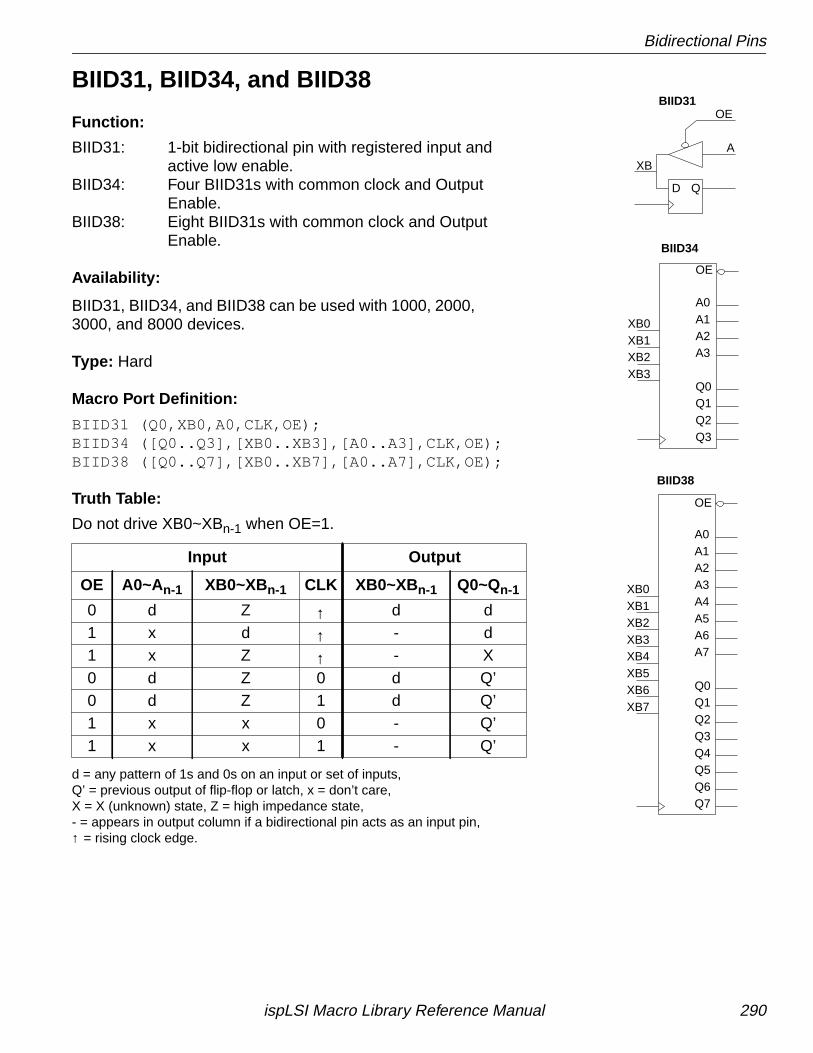
Bidirectional Pins
BIID31, BIID34, and BIID38
Function:
BIID31: 1-bit bidirectional pin with registered input andactive low enable.
BIID34: Four BIID31s with common clock and OutputEnable.
BIID38: Eight BIID31s with common clock and OutputEnable.
Availability:
BIID31, BIID34, and BIID38 can be used with 1000, 2000,3000, and 8000 devices.
Type: Hard
Macro Port Definition:
BIID31 (Q0,XB0,A0,CLK,OE);BIID34 ([Q0..Q3],[XB0..XB3],[A0..A3],CLK,OE);BIID38 ([Q0..Q7],[XB0..XB7],[A0..A7],CLK,OE);
Truth Table:
Do not drive XB0~XBn-1 when OE=1.
d = any pattern of 1s and 0s on an input or set of inputs,Q’ = previous output of flip-flop or latch, x = don’t care,X = X (unknown) state, Z = high impedance state,- = appears in output column if a bidirectional pin acts as an input pin,↑ = rising clock edge.
Input Output
OE A0~An-1 XB0~XBn-1 CLK XB0~XB n-1 Q0~Qn-1
0 d Z ↑ d d1 x d ↑ - d1 x Z ↑ - X0 d Z 0 d Q’0 d Z 1 d Q’1 x x 0 - Q’1 x x 1 - Q’
BIID31
BIID34
BIID38
D
A
Q
XB
OE
XB3
Q3
Q1Q0
XB0XB1
A3A2A1
OE
A0
Q2
XB2
OE
A0
XB2XB1XB0
XB3
Q2
Q0Q1
Q3
A4
A6
Q7
Q5Q4
XB4XB5
A3A2A1
Q6
XB6XB7
A5
A7
ispLSI Macro Library Reference Manual 290
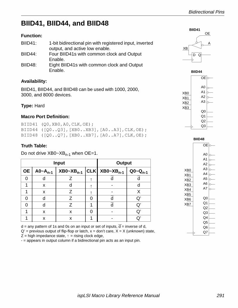
Bidirectional Pins
BIID41, BIID44, and BIID48
Function:
BIID41: 1-bit bidirectional pin with registered input, invertedoutput, and active low enable.
BIID44: Four BIID41s with common clock and OutputEnable.
BIID48: Eight BIID41s with common clock and OutputEnable.
Availability:
BIID41, BIID44, and BIID48 can be used with 1000, 2000,3000, and 8000 devices.
Type: Hard
Macro Port Definition:
BIID41 (Q0,XB0,A0,CLK,OE);BIID44 ([Q0..Q3],[XB0..XB3],[A0..A3],CLK,OE);BIID48 ([Q0..Q7],[XB0..XB7],[A0..A7],CLK,OE);
Truth Table:
Do not drive XB0~XBn-1 when OE=1.
d = any pattern of 1s and 0s on an input or set of inputs, d = inverse of d,Q’ = previous output of flip-flop or latch, x = don’t care, X = X (unknown) state,Z = high impedance state, ↑ = rising clock edge,- = appears in output column if a bidirectional pin acts as an input pin.
Input Output
OE A0~An-1 XB0~XBn-1 CLK XB0~XB n-1 Q0~Qn-1
0 d Z ↑ d d1 x d ↑ - d1 x Z ↑ - X0 d Z 0 d Q’0 d Z 1 d Q’1 x x 0 - Q’1 x x 1 - Q’
BIID41
BIID44
BIID48
D
A
Q
XB
OE
XB3
Q3
Q1Q0
XB0XB1
A3A2A1
OE
A0
Q2
XB2
OE
A0
XB2XB1XB0
XB3
Q2
Q0Q1
Q3
A4
A6
Q7
Q5Q4
XB4XB5
A3A2A1
Q6
XB6XB7
A5
A7
ispLSI Macro Library Reference Manual 291
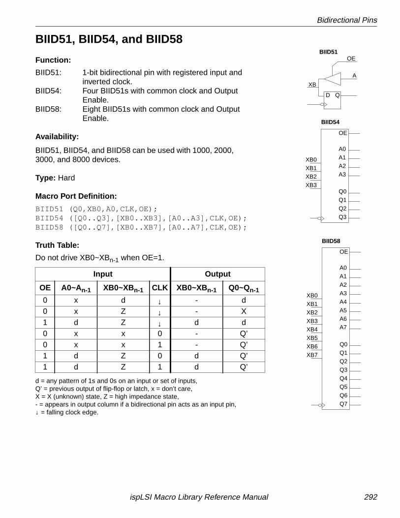
Bidirectional Pins
BIID51, BIID54, and BIID58
Function:
BIID51: 1-bit bidirectional pin with registered input andinverted clock.
BIID54: Four BIID51s with common clock and OutputEnable.
BIID58: Eight BIID51s with common clock and OutputEnable.
Availability:
BIID51, BIID54, and BIID58 can be used with 1000, 2000,3000, and 8000 devices.
Type: Hard
Macro Port Definition:
BIID51 (Q0,XB0,A0,CLK,OE);BIID54 ([Q0..Q3],[XB0..XB3],[A0..A3],CLK,OE);BIID58 ([Q0..Q7],[XB0..XB7],[A0..A7],CLK,OE);
Truth Table:
Do not drive XB0~XBn-1 when OE=1.
d = any pattern of 1s and 0s on an input or set of inputs,Q’ = previous output of flip-flop or latch, x = don’t care,X = X (unknown) state, Z = high impedance state,- = appears in output column if a bidirectional pin acts as an input pin,↓ = falling clock edge.
Input Output
OE A0~An-1 XB0~XBn-1 CLK XB0~XB n-1 Q0~Qn-1
0 x d ↓ - d0 x Z ↓ - X1 d Z ↓ d d0 x x 0 - Q’0 x x 1 - Q’1 d Z 0 d Q’1 d Z 1 d Q’
BIID51
BIID54
BIID58
D
A
Q
XB
OE
XB3
Q3
Q1Q0
XB0
XB1A3A2A1
OE
A0
Q2
XB2
OE
A0
XB2XB1
XB0
XB3
Q2
Q0Q1
Q3
A4
A6
Q7
Q5Q4
XB4
XB5
A3
A2A1
Q6
XB6
XB7
A5
A7
ispLSI Macro Library Reference Manual 292
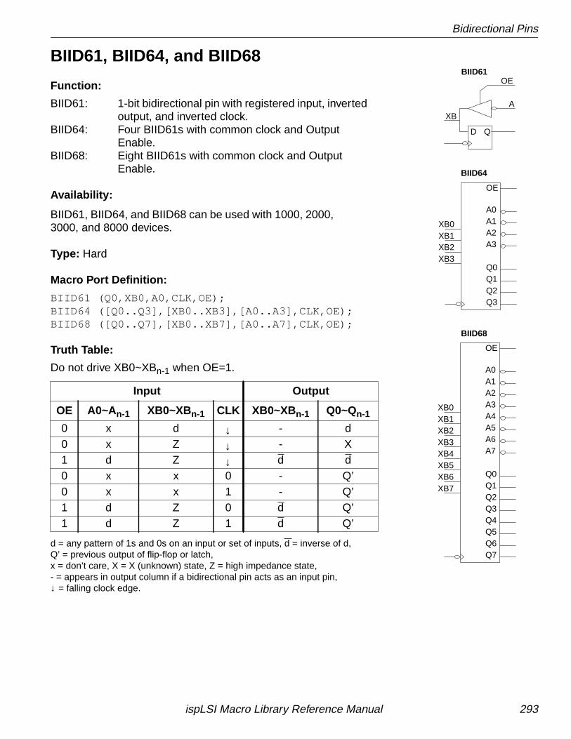
Bidirectional Pins
BIID61, BIID64, and BIID68
Function:
BIID61: 1-bit bidirectional pin with registered input, invertedoutput, and inverted clock.
BIID64: Four BIID61s with common clock and OutputEnable.
BIID68: Eight BIID61s with common clock and OutputEnable.
Availability:
BIID61, BIID64, and BIID68 can be used with 1000, 2000,3000, and 8000 devices.
Type: Hard
Macro Port Definition:
BIID61 (Q0,XB0,A0,CLK,OE);BIID64 ([Q0..Q3],[XB0..XB3],[A0..A3],CLK,OE);BIID68 ([Q0..Q7],[XB0..XB7],[A0..A7],CLK,OE);
Truth Table:
Do not drive XB0~XBn-1 when OE=1.
d = any pattern of 1s and 0s on an input or set of inputs, d = inverse of d,Q’ = previous output of flip-flop or latch,x = don’t care, X = X (unknown) state, Z = high impedance state,- = appears in output column if a bidirectional pin acts as an input pin,↓ = falling clock edge.
Input Output
OE A0~An-1 XB0~XBn-1 CLK XB0~XB n-1 Q0~Qn-1
0 x d ↓ - d0 x Z ↓ - X1 d Z ↓ d d0 x x 0 - Q’0 x x 1 - Q’1 d Z 0 d Q’1 d Z 1 d Q’
BIID61
BIID64
BIID68
D
A
Q
XB
OE
XB3
Q3
Q1Q0
XB0XB1
A3A2A1
OE
A0
Q2
XB2
OE
A0
XB2XB1XB0
XB3
Q2
Q0Q1
Q3
A4
A6
Q7
Q5Q4
XB4XB5
A3A2A1
Q6
XB6XB7
A5
A7
ispLSI Macro Library Reference Manual 293
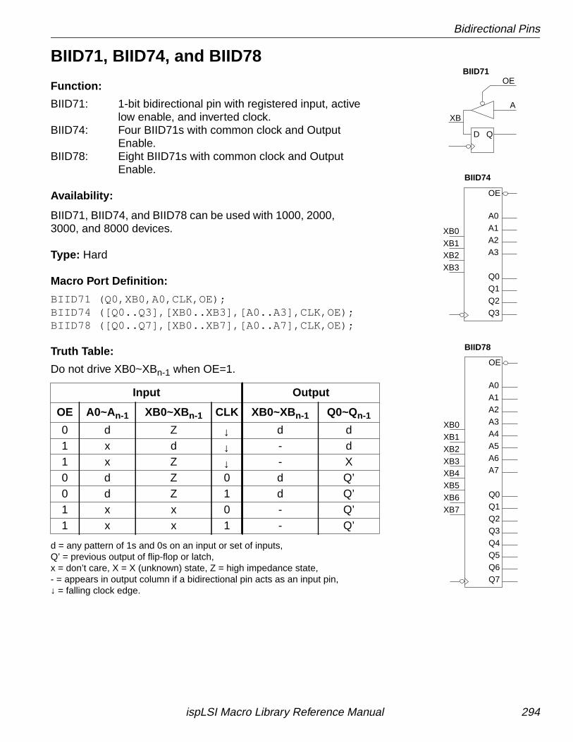
Bidirectional Pins
BIID71, BIID74, and BIID78
Function:
BIID71: 1-bit bidirectional pin with registered input, activelow enable, and inverted clock.
BIID74: Four BIID71s with common clock and OutputEnable.
BIID78: Eight BIID71s with common clock and OutputEnable.
Availability:
BIID71, BIID74, and BIID78 can be used with 1000, 2000,3000, and 8000 devices.
Type: Hard
Macro Port Definition:
BIID71 (Q0,XB0,A0,CLK,OE);BIID74 ([Q0..Q3],[XB0..XB3],[A0..A3],CLK,OE);BIID78 ([Q0..Q7],[XB0..XB7],[A0..A7],CLK,OE);
Truth Table:
Do not drive XB0~XBn-1 when OE=1.
d = any pattern of 1s and 0s on an input or set of inputs,Q’ = previous output of flip-flop or latch,x = don’t care, X = X (unknown) state, Z = high impedance state,- = appears in output column if a bidirectional pin acts as an input pin,↓ = falling clock edge.
Input Output
OE A0~An-1 XB0~XBn-1 CLK XB0~XB n-1 Q0~Qn-1
0 d Z ↓ d d1 x d ↓ - d1 x Z ↓ - X0 d Z 0 d Q’0 d Z 1 d Q’1 x x 0 - Q’1 x x 1 - Q’
BIID71
BIID74
BIID78
D
A
Q
XB
OE
XB3
Q3
Q1Q0
XB0
XB1A3A2A1
OE
A0
Q2
XB2
OE
A0
XB2XB1
XB0
XB3
Q2
Q0Q1
Q3
A4
A6
Q7
Q5Q4
XB4
XB5
A3A2A1
Q6
XB6
XB7
A5
A7
ispLSI Macro Library Reference Manual 294
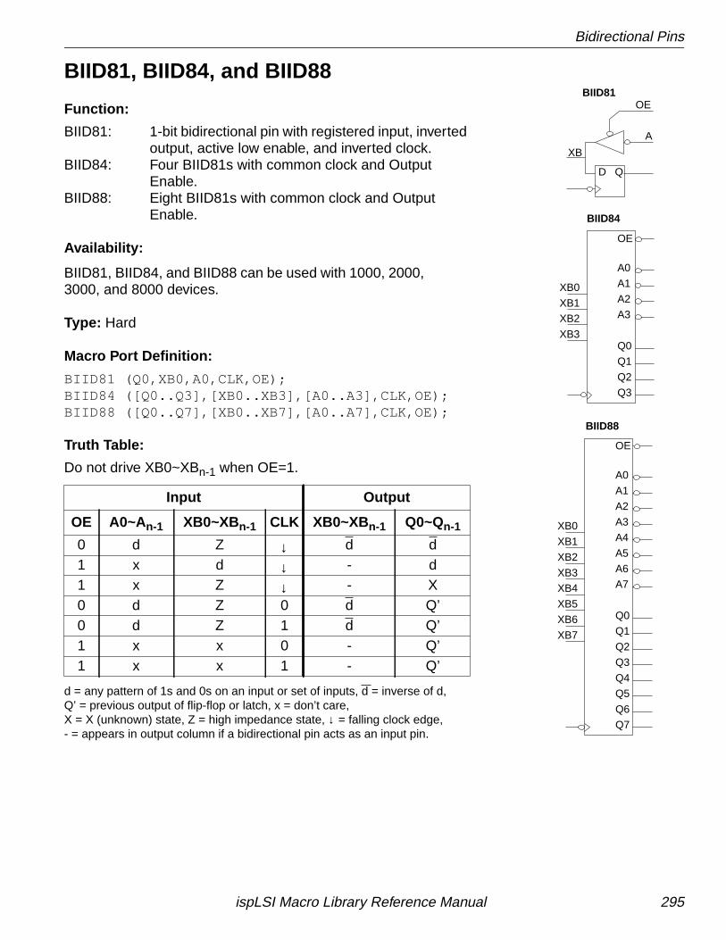
Bidirectional Pins
BIID81, BIID84, and BIID88
Function:
BIID81: 1-bit bidirectional pin with registered input, invertedoutput, active low enable, and inverted clock.
BIID84: Four BIID81s with common clock and OutputEnable.
BIID88: Eight BIID81s with common clock and OutputEnable.
Availability:
BIID81, BIID84, and BIID88 can be used with 1000, 2000,3000, and 8000 devices.
Type: Hard
Macro Port Definition:
BIID81 (Q0,XB0,A0,CLK,OE);BIID84 ([Q0..Q3],[XB0..XB3],[A0..A3],CLK,OE);BIID88 ([Q0..Q7],[XB0..XB7],[A0..A7],CLK,OE);
Truth Table:
Do not drive XB0~XBn-1 when OE=1.
d = any pattern of 1s and 0s on an input or set of inputs, d = inverse of d,Q’ = previous output of flip-flop or latch, x = don’t care,X = X (unknown) state, Z = high impedance state, ↓ = falling clock edge,- = appears in output column if a bidirectional pin acts as an input pin.
Input Output
OE A0~An-1 XB0~XBn-1 CLK XB0~XB n-1 Q0~Qn-1
0 d Z ↓ d d1 x d ↓ - d1 x Z ↓ - X0 d Z 0 d Q’0 d Z 1 d Q’1 x x 0 - Q’1 x x 1 - Q’
D
A
Q
XB
OEBIID81
BIID84
BIID88
XB3
Q3
Q1
Q0
XB0
XB1A3
A2
A1
OE
A0
Q2
XB2
OE
A0
XB2
XB1
XB0
XB3
Q2
Q0
Q1
Q3
A4
A6
Q7
Q5
Q4
XB4
XB5
A3
A2
A1
Q6
XB6
XB7
A5
A7
ispLSI Macro Library Reference Manual 295
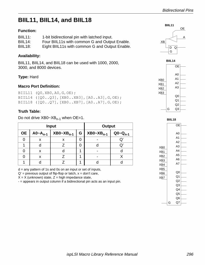
Bidirectional Pins
BIIL11, BIIL14, and BIIL18
Function:
BIIL11: 1-bit bidirectional pin with latched input.BIIL14: Four BIIL11s with common G and Output Enable.BIIL18: Eight BIIL11s with common G and Output Enable.
Availability:
BIIL11, BIIL14, and BIIL18 can be used with 1000, 2000,3000, and 8000 devices.
Type: Hard
Macro Port Definition:
BIIL11 (Q0,XB0,A0,G,OE);BIIL14 ([Q0..Q3],[XB0..XB3],[A0..A3],G,OE);BIIL18 ([Q0..Q7],[XB0..XB7],[A0..A7],G,OE);
Truth Table:
Do not drive XB0~XBn-1 when OE=1.
d = any pattern of 1s and 0s on an input or set of inputs,Q’ = previous output of flip-flop or latch, x = don’t care,X = X (unknown) state, Z = high impedance state,- = appears in output column if a bidirectional pin acts as an input pin.
Input Output
OE A0~An-1 XB0~XBn-1 G XB0~XBn-1 Q0~Qn-1
0 x x 0 - Q’1 d Z 0 d Q’0 x d 1 - d0 x Z 1 - X1 d Z 1 d d
BIIL11
BIIL14
BIIL18
D
A
Q
XB
OE
XB3
Q3
Q1Q0
XB0XB1
A3A2A1
OE
A0
Q2
XB2
OE
A0
XB2XB1XB0
XB3
Q2
Q0Q1
Q3
A4
A6
Q7
Q5Q4
XB4XB5
A3A2A1
Q6
XB6XB7
A5
A7
G
G
G
ispLSI Macro Library Reference Manual 296
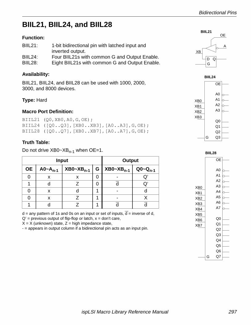
Bidirectional Pins
BIIL21, BIIL24, and BIIL28
Function:
BIIL21: 1-bit bidirectional pin with latched input andinverted output.
BIIL24: Four BIIL21s with common G and Output Enable.BIIL28: Eight BIIL21s with common G and Output Enable.
Availability:
BIIL21, BIIL24, and BIIL28 can be used with 1000, 2000,3000, and 8000 devices.
Type: Hard
Macro Port Definition:
BIIL21 (Q0,XB0,A0,G,OE);BIIL24 ([Q0..Q3],[XB0..XB3],[A0..A3],G,OE);BIIL28 ([Q0..Q7],[XB0..XB7],[A0..A7],G,OE);
Truth Table:
Do not drive XB0~XBn-1 when OE=1.
d = any pattern of 1s and 0s on an input or set of inputs, d = inverse of d,Q’ = previous output of flip-flop or latch, x = don’t care,X = X (unknown) state, Z = high impedance state,- = appears in output column if a bidirectional pin acts as an input pin.
Input Output
OE A0~An-1 XB0~XBn-1 G XB0~XBn-1 Q0~Qn-1
0 x x 0 - Q’1 d Z 0 d Q’0 x d 1 - d0 x Z 1 - X1 d Z 1 d d
BIIL21
BIIL24
BIIL28
D
A
Q
XB
OE
XB3
Q3
Q1
Q0
XB0
XB1A3
A2
A1
OE
A0
Q2
XB2
OE
A0
XB2
XB1
XB0
XB3
Q2
Q0
Q1
Q3
A4
A6
Q7
Q5
Q4
XB4
XB5
A3
A2
A1
Q6
XB6
XB7
A5
A7
G
G
G
ispLSI Macro Library Reference Manual 297
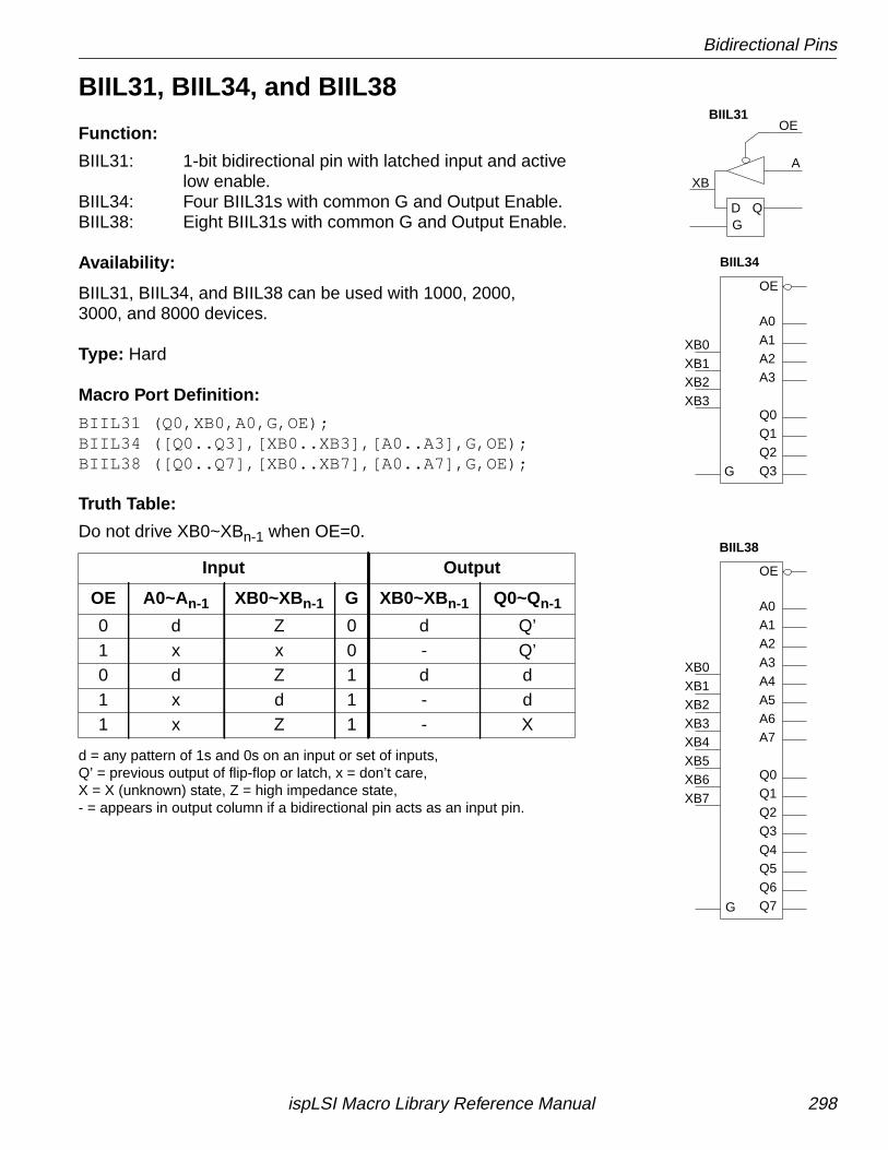
Bidirectional Pins
BIIL31, BIIL34, and BIIL38
Function:
BIIL31: 1-bit bidirectional pin with latched input and activelow enable.
BIIL34: Four BIIL31s with common G and Output Enable.BIIL38: Eight BIIL31s with common G and Output Enable.
Availability:
BIIL31, BIIL34, and BIIL38 can be used with 1000, 2000,3000, and 8000 devices.
Type: Hard
Macro Port Definition:
BIIL31 (Q0,XB0,A0,G,OE);BIIL34 ([Q0..Q3],[XB0..XB3],[A0..A3],G,OE);BIIL38 ([Q0..Q7],[XB0..XB7],[A0..A7],G,OE);
Truth Table:
Do not drive XB0~XBn-1 when OE=0.
d = any pattern of 1s and 0s on an input or set of inputs,Q’ = previous output of flip-flop or latch, x = don’t care,X = X (unknown) state, Z = high impedance state,- = appears in output column if a bidirectional pin acts as an input pin.
Input Output
OE A0~An-1 XB0~XBn-1 G XB0~XBn-1 Q0~Qn-1
0 d Z 0 d Q’1 x x 0 - Q’0 d Z 1 d d1 x d 1 - d1 x Z 1 - X
BIIL31
BIIL34
BIIL38
D
A
Q
XB
OE
XB3
Q3
Q1Q0
XB0XB1
A3A2A1
OE
A0
Q2
XB2
OE
A0
XB2XB1XB0
XB3
Q2
Q0Q1
Q3
A4
A6
Q7
Q5Q4
XB4XB5
A3A2A1
Q6
XB6XB7
A5
A7
G
G
G
ispLSI Macro Library Reference Manual 298
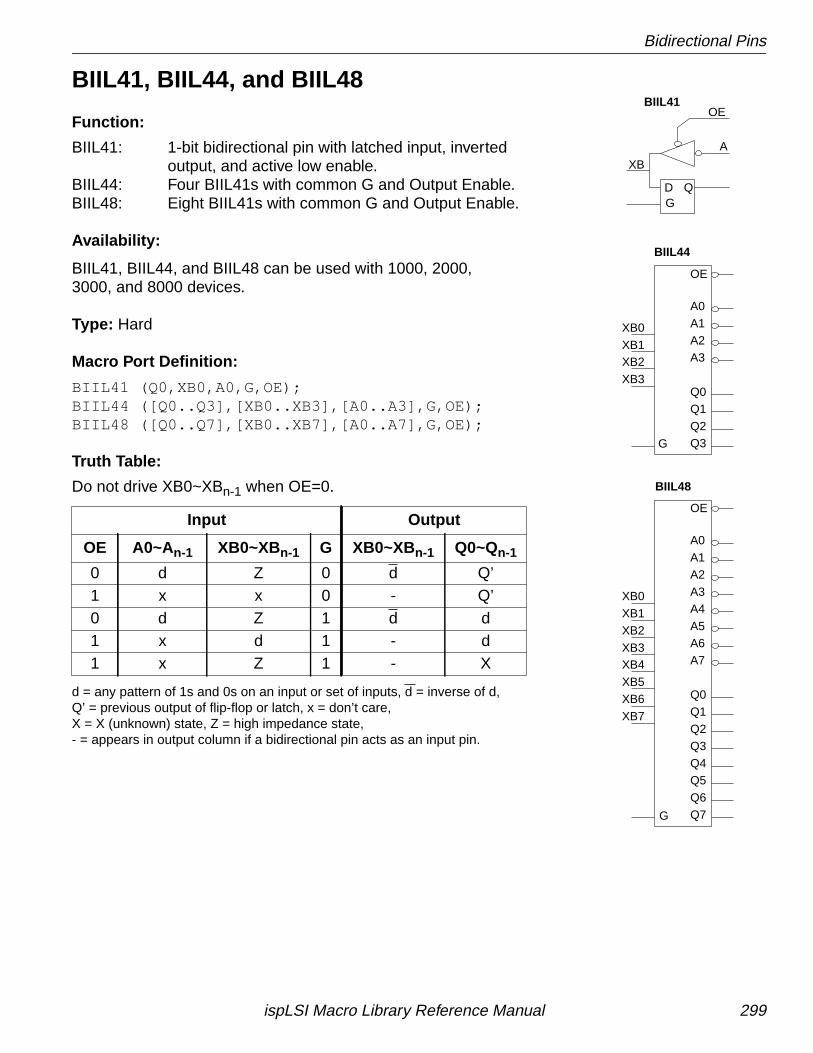
Bidirectional Pins
BIIL41, BIIL44, and BIIL48
Function:
BIIL41: 1-bit bidirectional pin with latched input, invertedoutput, and active low enable.
BIIL44: Four BIIL41s with common G and Output Enable.BIIL48: Eight BIIL41s with common G and Output Enable.
Availability:
BIIL41, BIIL44, and BIIL48 can be used with 1000, 2000,3000, and 8000 devices.
Type: Hard
Macro Port Definition:
BIIL41 (Q0,XB0,A0,G,OE);BIIL44 ([Q0..Q3],[XB0..XB3],[A0..A3],G,OE);BIIL48 ([Q0..Q7],[XB0..XB7],[A0..A7],G,OE);
Truth Table:
Do not drive XB0~XBn-1 when OE=0.
d = any pattern of 1s and 0s on an input or set of inputs, d = inverse of d,Q’ = previous output of flip-flop or latch, x = don’t care,X = X (unknown) state, Z = high impedance state,- = appears in output column if a bidirectional pin acts as an input pin.
Input Output
OE A0~An-1 XB0~XBn-1 G XB0~XBn-1 Q0~Qn-1
0 d Z 0 d Q’1 x x 0 - Q’0 d Z 1 d d1 x d 1 - d1 x Z 1 - X
BIIL41
BIIL44
BIIL48
D
A
Q
XB
OE
XB3
Q3
Q1Q0
XB0XB1
A3A2A1
OE
A0
Q2
XB2
OE
A0
XB2XB1XB0
XB3
Q2
Q0Q1
Q3
A4
A6
Q7
Q5Q4
XB4XB5
A3A2A1
Q6
XB6XB7
A5
A7
G
G
G
ispLSI Macro Library Reference Manual 299
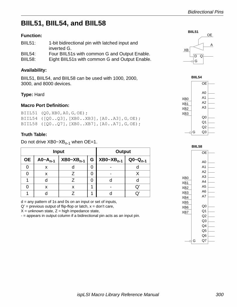
Bidirectional Pins
BIIL51, BIIL54, and BIIL58
Function:
BIIL51: 1-bit bidirectional pin with latched input andinverted G.
BIIL54: Four BIIL51s with common G and Output Enable.BIIL58: Eight BIIL51s with common G and Output Enable.
Availability:
BIIL51, BIIL54, and BIIL58 can be used with 1000, 2000,3000, and 8000 devices.
Type: Hard
Macro Port Definition:
BIIL51 (Q0,XB0,A0,G,OE);BIIL54 ([Q0..Q3],[XB0..XB3],[A0..A3],G,OE);BIIL58 ([Q0..Q7],[XB0..XB7],[A0..A7],G,OE);
Truth Table:
Do not drive XB0~XBn-1 when OE=1.
d = any pattern of 1s and 0s on an input or set of inputs,Q’ = previous output of flip-flop or latch, x = don’t care,X = unknown state, Z = high impedance state,- = appears in output column if a bidirectional pin acts as an input pin.
Input Output
OE A0~An-1 XB0~XBn-1 G XB0~XBn-1 Q0~Qn-1
0 x d 0 - d0 x Z 0 - X1 d Z 0 d d0 x x 1 - Q’1 d Z 1 d Q’
BIIL51
BIIL54
BIIL58
D
A
Q
XB
OE
XB3
Q3
Q1Q0
XB0XB1
A3A2A1
OE
A0
Q2
XB2
OE
A0
XB2XB1XB0
XB3
Q2
Q0Q1
Q3
A4
A6
Q7
Q5Q4
XB4XB5
A3A2A1
Q6
XB6XB7
A5
A7
G
G
G
ispLSI Macro Library Reference Manual 300
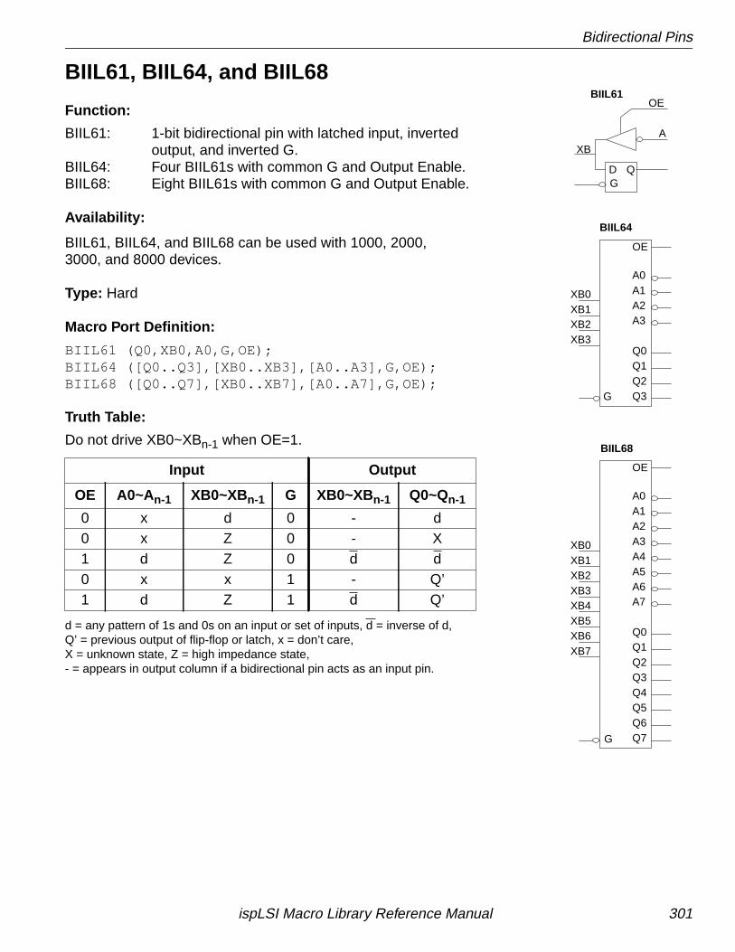
Bidirectional Pins
BIIL61, BIIL64, and BIIL68
Function:
BIIL61: 1-bit bidirectional pin with latched input, invertedoutput, and inverted G.
BIIL64: Four BIIL61s with common G and Output Enable.BIIL68: Eight BIIL61s with common G and Output Enable.
Availability:
BIIL61, BIIL64, and BIIL68 can be used with 1000, 2000,3000, and 8000 devices.
Type: Hard
Macro Port Definition:
BIIL61 (Q0,XB0,A0,G,OE);BIIL64 ([Q0..Q3],[XB0..XB3],[A0..A3],G,OE);BIIL68 ([Q0..Q7],[XB0..XB7],[A0..A7],G,OE);
Truth Table:
Do not drive XB0~XBn-1 when OE=1.
d = any pattern of 1s and 0s on an input or set of inputs, d = inverse of d,Q’ = previous output of flip-flop or latch, x = don’t care,X = unknown state, Z = high impedance state,- = appears in output column if a bidirectional pin acts as an input pin.
Input Output
OE A0~An-1 XB0~XBn-1 G XB0~XBn-1 Q0~Qn-1
0 x d 0 - d0 x Z 0 - X1 d Z 0 d d0 x x 1 - Q’1 d Z 1 d Q’
BIIL61
BIIL64
BIIL68
D
A
Q
XB
OE
XB3
Q3
Q1Q0
XB0XB1
A3A2A1
OE
A0
Q2
XB2
OE
A0
XB2XB1XB0
XB3
Q2
Q0Q1
Q3
A4
A6
Q7
Q5Q4
XB4XB5
A3A2A1
Q6
XB6XB7
A5
A7
G
G
G
ispLSI Macro Library Reference Manual 301
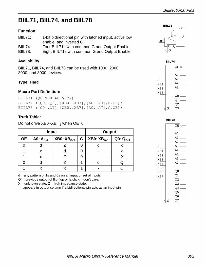
Bidirectional Pins
BIIL71, BIIL74, and BIIL78
Function:
BIIL71: 1-bit bidirectional pin with latched input, active lowenable, and inverted G.
BIIL74: Four BIIL71s with common G and Output Enable.BIIL78: Eight BIIL71s with common G and Output Enable.
Availability:
BIIL71, BIIL74, and BIIL78 can be used with 1000, 2000,3000, and 8000 devices.
Type: Hard
Macro Port Definition:
BIIL71 (Q0,XB0,A0,G,OE);BIIL74 ([Q0..Q3],[XB0..XB3],[A0..A3],G,OE);BIIL78 ([Q0..Q7],[XB0..XB7],[A0..A7],G,OE);
Truth Table:
Do not drive XB0~XBn-1 when OE=0.
d = any pattern of 1s and 0s on an input or set of inputs,Q’ = previous output of flip-flop or latch, x = don’t care,X = unknown state, Z = high impedance state,- = appears in output column if a bidirectional pin acts as an input pin.
Input Output
OE A0~An-1 XB0~XBn-1 G XB0~XBn-1 Q0~Qn-1
0 d Z 0 d d1 x d 0 - d1 x Z 0 - X0 d Z 1 d Q’1 x x 1 - Q’
BIIL71
BIIL74
BIIL78
D
A
Q
XB
OE
XB3
Q3
Q1Q0
XB0XB1
A3A2A1
OE
A0
Q2
XB2
OE
A0
XB2XB1XB0
XB3
Q2
Q0Q1
Q3
A4
A6
Q7
Q5Q4
XB4XB5
A3A2A1
Q6
XB6XB7
A5
A7
G
G
G
ispLSI Macro Library Reference Manual 302
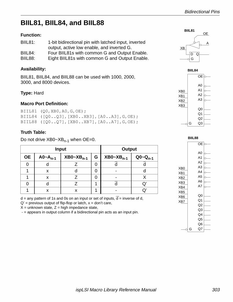
Bidirectional Pins
BIIL81, BIIL84, and BIIL88
Function:
BIIL81: 1-bit bidirectional pin with latched input, invertedoutput, active low enable, and inverted G.
BIIL84: Four BIIL81s with common G and Output Enable.BIIL88: Eight BIIL81s with common G and Output Enable.
Availability:
BIIL81, BIIL84, and BIIL88 can be used with 1000, 2000,3000, and 8000 devices.
Type: Hard
Macro Port Definition:
BIIL81 (Q0,XB0,A0,G,OE);BIIL84 ([Q0..Q3],[XB0..XB3],[A0..A3],G,OE);BIIL88 ([Q0..Q7],[XB0..XB7],[A0..A7],G,OE);
Truth Table:
Do not drive XB0~XBn-1 when OE=0.
d = any pattern of 1s and 0s on an input or set of inputs, d = inverse of d,Q’ = previous output of flip-flop or latch, x = don’t care,X = unknown state, Z = high impedance state, - = appears in output column if a bidirectional pin acts as an input pin.
Input Output
OE A0~An-1 XB0~XBn-1 G XB0~XBn-1 Q0~Qn-1
0 d Z 0 d d1 x d 0 - d1 x Z 0 - X0 d Z 1 d Q’1 x x 1 - Q’
BIIL81
BIIL84
BIIL88
D
A
Q
XB
OE
XB3
Q3
Q1Q0
XB0XB1
A3A2A1
OE
A0
Q2
XB2
OE
A0
XB2XB1XB0
XB3
Q2
Q0Q1
Q3
A4
A6
Q7
Q5Q4
XB4XB5
A3A2A1
Q6
XB6XB7
A5
A7
G
G
G
ispLSI Macro Library Reference Manual 303
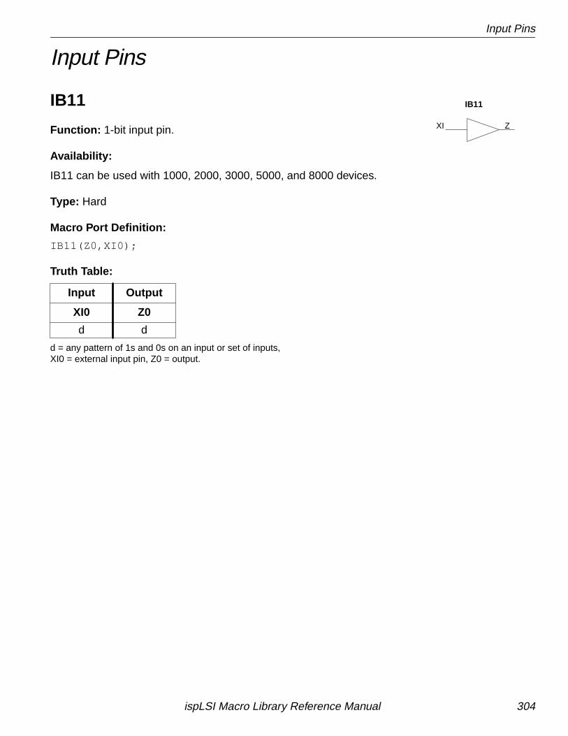
Input Pins
Input Pins
IB11
Function: 1-bit input pin.
Availability:
IB11 can be used with 1000, 2000, 3000, 5000, and 8000 devices.
Type: Hard
Macro Port Definition:
IB11(Z0,XI0);
Truth Table:
d = any pattern of 1s and 0s on an input or set of inputs,XI0 = external input pin, Z0 = output.
Input Output
XI0 Z0
d d
XI Z
IB11
ispLSI Macro Library Reference Manual 304
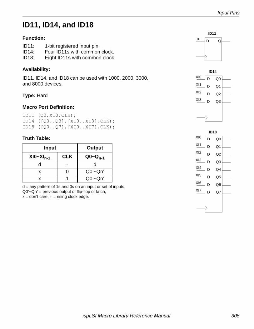
Input Pins
ID11, ID14, and ID18
Function:
ID11: 1-bit registered input pin.ID14: Four ID11s with common clock.ID18: Eight ID11s with common clock.
Availability:
ID11, ID14, and ID18 can be used with 1000, 2000, 3000,and 8000 devices.
Type: Hard
Macro Port Definition:
ID11 (Q0,XI0,CLK);ID14 ([Q0..Q3],[XI0..XI3],CLK);ID18 ([Q0..Q7],[XI0..XI7],CLK);
Truth Table:
d = any pattern of 1s and 0s on an input or set of inputs,Q0’~Qn’ = previous output of flip-flop or latch,x = don’t care, ↑ = rising clock edge.
Input Output
XI0~XIn-1 CLK Q0~Qn-1
d ↑ dx 0 Q0’~Qn’x 1 Q0’~Qn’
DXI Q
ID11
ID14
ID18
D
D
D
D
XI0
XI1
XI2
Q0
Q1
Q2
Q3XI3
D
D
D
D
D
D
D
D
Q0
Q1
Q2
Q3XI3
XI2
XI1
XI0
XI4
XI5
XI6
XI7 Q7
Q6
Q5
Q4
ispLSI Macro Library Reference Manual 305
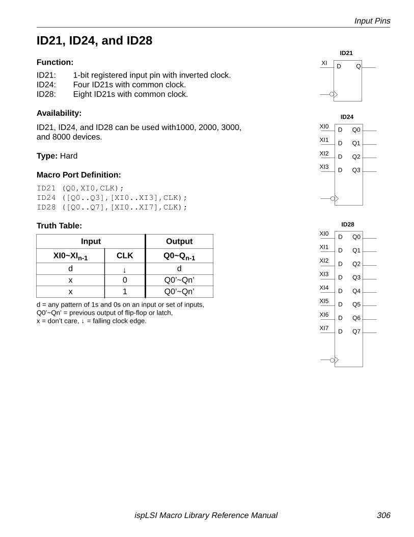
Input Pins
ID21, ID24, and ID28
Function:
ID21: 1-bit registered input pin with inverted clock.ID24: Four ID21s with common clock.ID28: Eight ID21s with common clock.
Availability:
ID21, ID24, and ID28 can be used with1000, 2000, 3000,and 8000 devices.
Type: Hard
Macro Port Definition:
ID21 (Q0,XI0,CLK);ID24 ([Q0..Q3],[XI0..XI3],CLK);ID28 ([Q0..Q7],[XI0..XI7],CLK);
Truth Table:
d = any pattern of 1s and 0s on an input or set of inputs,Q0’~Qn’ = previous output of flip-flop or latch,x = don’t care, ↓ = falling clock edge.
Input Output
XI0~XIn-1 CLK Q0~Qn-1
d ↓ dx 0 Q0’~Qn’x 1 Q0’~Qn’
DXI Q
ID21
ID24
ID28
D
D
D
D
XI0
XI1
XI2
Q0
Q1
Q2
Q3XI3
D
D
D
D
D
D
D
D
Q0
Q1
Q2
Q3XI3
XI2
XI1
XI0
XI4
XI5
XI6
XI7 Q7
Q6
Q5
Q4
ispLSI Macro Library Reference Manual 306
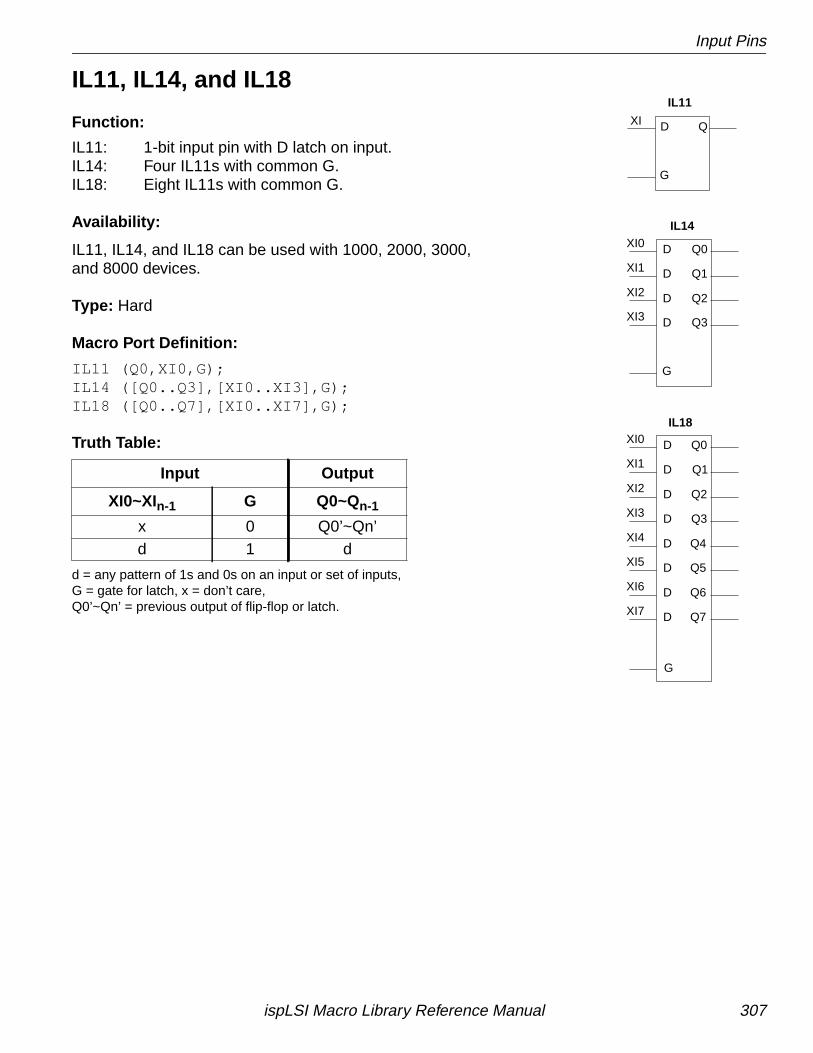
Input Pins
IL11, IL14, and IL18
Function:
IL11: 1-bit input pin with D latch on input.IL14: Four IL11s with common G.IL18: Eight IL11s with common G.
Availability:
IL11, IL14, and IL18 can be used with 1000, 2000, 3000,and 8000 devices.
Type: Hard
Macro Port Definition:
IL11 (Q0,XI0,G);IL14 ([Q0..Q3],[XI0..XI3],G);IL18 ([Q0..Q7],[XI0..XI7],G);
Truth Table:
d = any pattern of 1s and 0s on an input or set of inputs,G = gate for latch, x = don’t care,Q0’~Qn’ = previous output of flip-flop or latch.
Input Output
XI0~XIn-1 G Q0~Qn-1
x 0 Q0’~Qn’d 1 d
DXI Q
IL11
IL14
IL18
D
D
D
D
XI0
XI1
XI2
Q0
Q1
Q2
Q3XI3
D
D
D
D
D
D
D
D
Q0
Q1
Q2
Q3XI3
XI2
XI1
XI0
XI4
XI5
XI6
XI7 Q7
Q6
Q5
Q4
G
G
G
ispLSI Macro Library Reference Manual 307
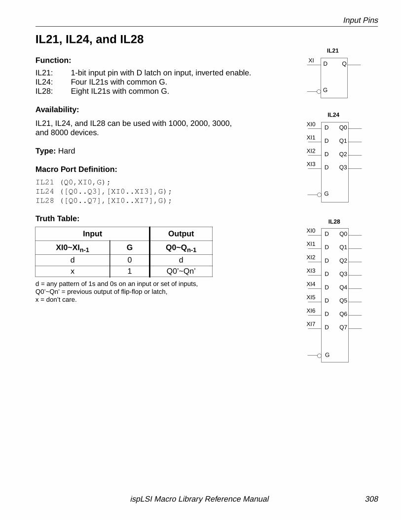
Input Pins
IL21, IL24, and IL28
Function:
IL21: 1-bit input pin with D latch on input, inverted enable.IL24: Four IL21s with common G.IL28: Eight IL21s with common G.
Availability:
IL21, IL24, and IL28 can be used with 1000, 2000, 3000,and 8000 devices.
Type: Hard
Macro Port Definition:
IL21 (Q0,XI0,G);IL24 ([Q0..Q3],[XI0..XI3],G);IL28 ([Q0..Q7],[XI0..XI7],G);
Truth Table:
d = any pattern of 1s and 0s on an input or set of inputs,Q0’~Qn’ = previous output of flip-flop or latch,x = don’t care.
Input Output
XI0~XIn-1 G Q0~Qn-1
d 0 dx 1 Q0’~Qn’
DXI Q
IL21
IL24
IL28
D
D
D
D
XI0
XI1
XI2
Q0
Q1
Q2
Q3XI3
D
D
D
D
D
D
D
D
Q0
Q1
Q2
Q3XI3
XI2
XI1
XI0
XI4
XI5
XI6
XI7 Q7
Q6
Q5
Q4
G
G
G
ispLSI Macro Library Reference Manual 308
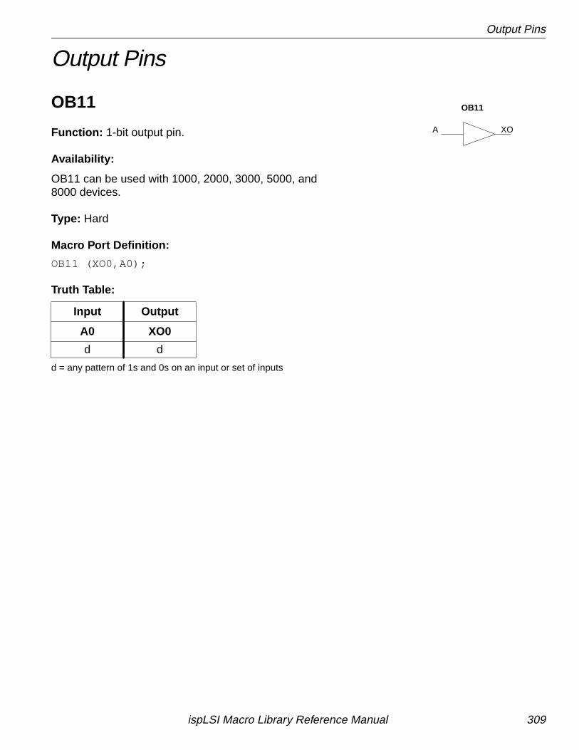
Output Pins
Output Pins
OB11
Function: 1-bit output pin.
Availability:
OB11 can be used with 1000, 2000, 3000, 5000, and8000 devices.
Type: Hard
Macro Port Definition:
OB11 (XO0,A0);
Truth Table:
d = any pattern of 1s and 0s on an input or set of inputs
Input Output
A0 XO0
d d
A XO
OB11
ispLSI Macro Library Reference Manual 309
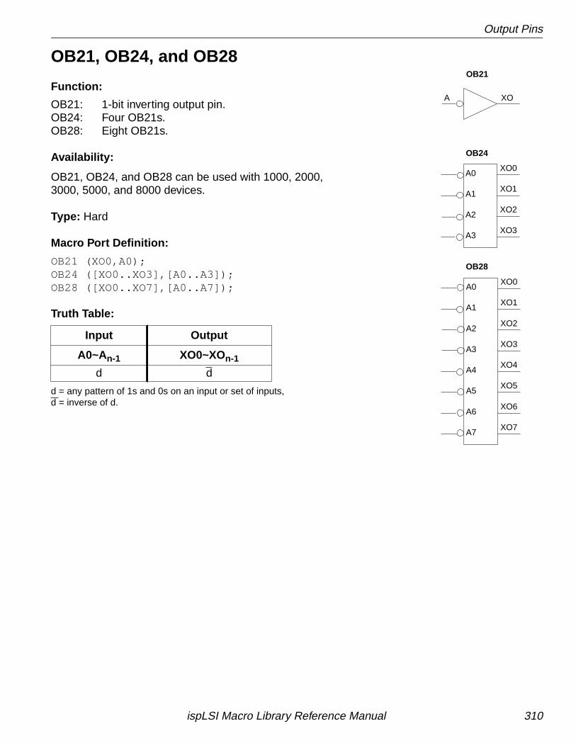
Output Pins
OB21, OB24, and OB28
Function:
OB21: 1-bit inverting output pin.OB24: Four OB21s.OB28: Eight OB21s.
Availability:
OB21, OB24, and OB28 can be used with 1000, 2000,3000, 5000, and 8000 devices.
Type: Hard
Macro Port Definition:
OB21 (XO0,A0);OB24 ([XO0..XO3],[A0..A3]);OB28 ([XO0..XO7],[A0..A7]);
Truth Table:
d = any pattern of 1s and 0s on an input or set of inputs,d = inverse of d.
Input Output
A0~An-1 XO0~XOn-1
d d
A XO
OB21
XO0A0
XO1A1
XO2A2
A3XO3
OB24
XO0
XO1
XO2
XO3A3
A2
A1
A0
A4
A5
A6
A7XO7
XO6
XO5
XO4
OB28
ispLSI Macro Library Reference Manual 310
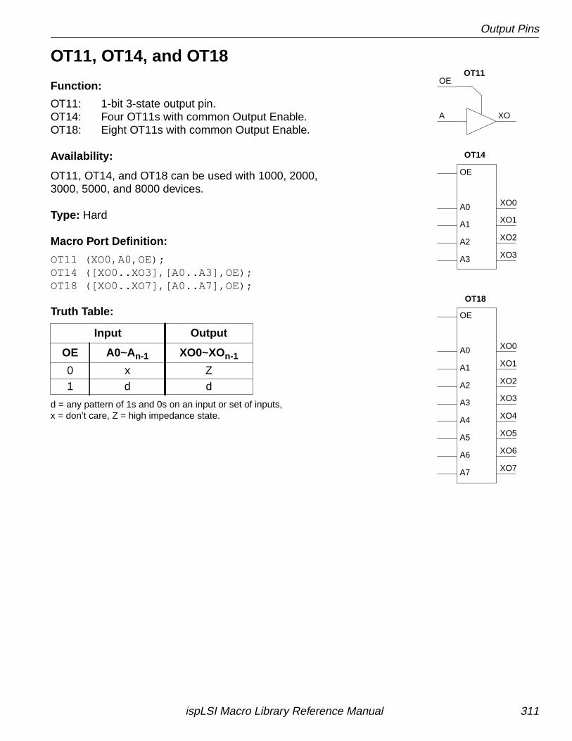
Output Pins
OT11, OT14, and OT18
Function:
OT11: 1-bit 3-state output pin.OT14: Four OT11s with common Output Enable.OT18: Eight OT11s with common Output Enable.
Availability:
OT11, OT14, and OT18 can be used with 1000, 2000,3000, 5000, and 8000 devices.
Type: Hard
Macro Port Definition:
OT11 (XO0,A0,OE);OT14 ([XO0..XO3],[A0..A3],OE);OT18 ([XO0..XO7],[A0..A7],OE);
Truth Table:
d = any pattern of 1s and 0s on an input or set of inputs,x = don’t care, Z = high impedance state.
Input Output
OE A0~An-1 XO0~XOn-1
0 x Z1 d d
OT11
XOA
OE
XO3A3
XO2A2
XO1A1
OE
A0 XO0
OT14
XO3A3
XO2A2
XO1A1
A0 XO0
XO4A4
A5 XO5
A6 XO6
A7 XO7
OE
OT18
ispLSI Macro Library Reference Manual 311
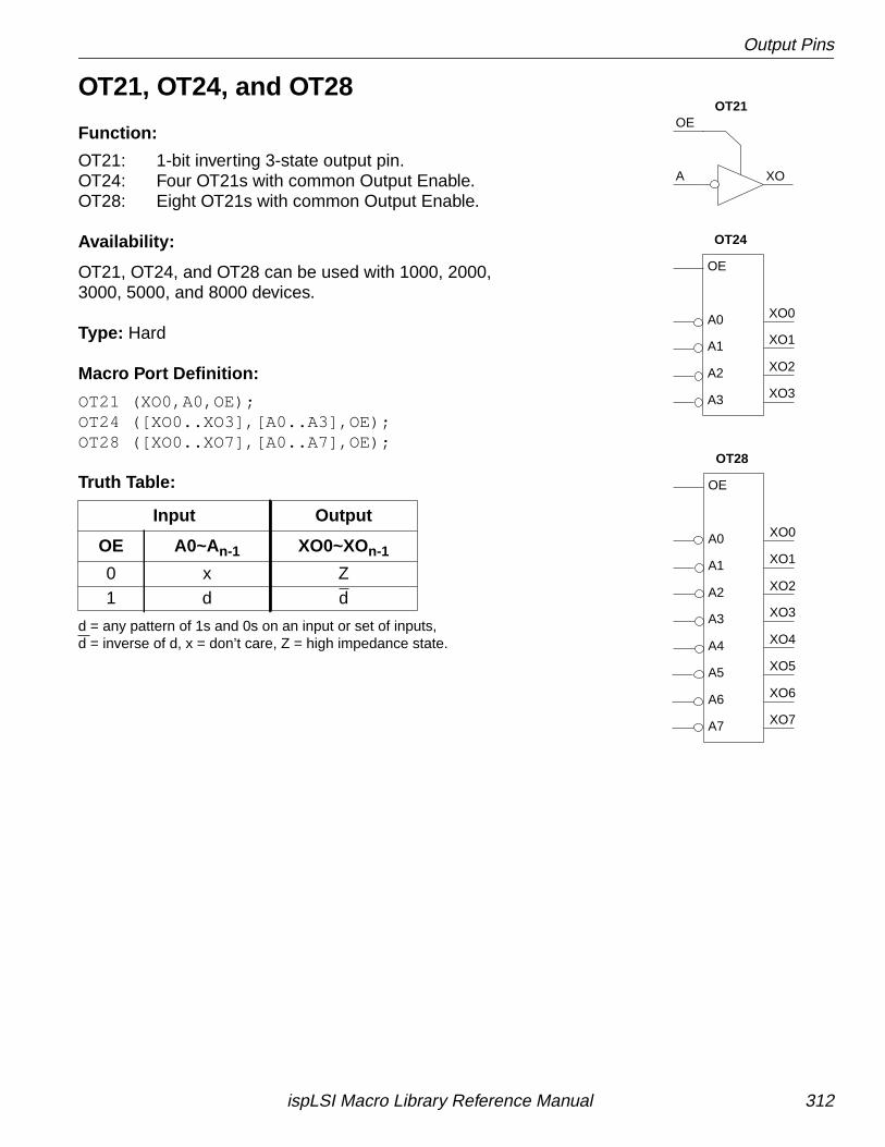
Output Pins
OT21, OT24, and OT28
Function:
OT21: 1-bit inverting 3-state output pin.OT24: Four OT21s with common Output Enable.OT28: Eight OT21s with common Output Enable.
Availability:
OT21, OT24, and OT28 can be used with 1000, 2000,3000, 5000, and 8000 devices.
Type: Hard
Macro Port Definition:
OT21 (XO0,A0,OE);OT24 ([XO0..XO3],[A0..A3],OE);OT28 ([XO0..XO7],[A0..A7],OE);
Truth Table:
d = any pattern of 1s and 0s on an input or set of inputs,d = inverse of d, x = don’t care, Z = high impedance state.
Input Output
OE A0~An-1 XO0~XOn-1
0 x Z1 d d
XO3A3
XO2A2
XO1A1
OE
A0 XO0
OT21
XOA
OE
OT24
XO3A3
XO2A2
XO1A1
A0 XO0
XO4A4
A5 XO5
A6 XO6
A7 XO7
OE
OT28
ispLSI Macro Library Reference Manual 312
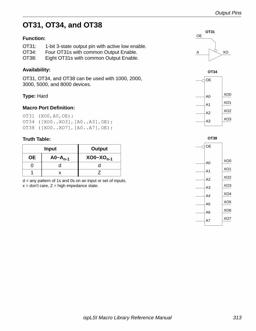
Output Pins
OT31, OT34, and OT38
Function:
OT31: 1-bit 3-state output pin with active low enable.OT34: Four OT31s with common Output Enable.OT38: Eight OT31s with common Output Enable.
Availability:
OT31, OT34, and OT38 can be used with 1000, 2000,3000, 5000, and 8000 devices.
Type: Hard
Macro Port Definition:
OT31 (XO0,A0,OE);OT34 ([XO0..XO3],[A0..A3],OE);OT38 ([XO0..XO7],[A0..A7],OE);
Truth Table:
d = any pattern of 1s and 0s on an input or set of inputs,x = don’t care, Z = high impedance state.
Input Output
OE A0~An-1 XO0~XOn-1
0 d d1 x Z
OT31
XOA
OE
XO3A3
XO2A2
XO1A1
OE
A0 XO0
OT34
XO3A3
XO2A2
XO1A1
A0 XO0
XO4A4
A5 XO5
A6 XO6
A7 XO7
OE
OT38
ispLSI Macro Library Reference Manual 313
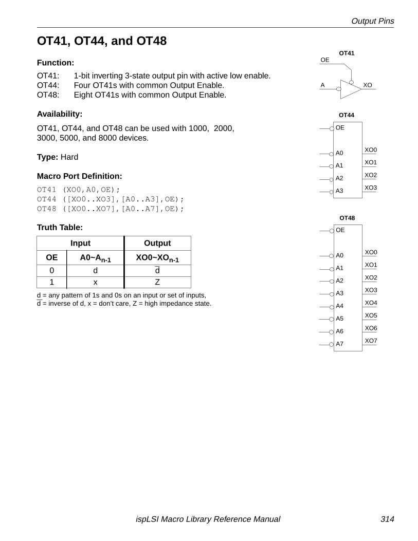
Output Pins
OT41, OT44, and OT48
Function:
OT41: 1-bit inverting 3-state output pin with active low enable.OT44: Four OT41s with common Output Enable.OT48: Eight OT41s with common Output Enable.
Availability:
OT41, OT44, and OT48 can be used with 1000, 2000,3000, 5000, and 8000 devices.
Type: Hard
Macro Port Definition:
OT41 (XO0,A0,OE);OT44 ([XO0..XO3],[A0..A3],OE);OT48 ([XO0..XO7],[A0..A7],OE);
Truth Table:
d = any pattern of 1s and 0s on an input or set of inputs,d = inverse of d, x = don’t care, Z = high impedance state.
Input Output
OE A0~An-1 XO0~XOn-1
0 d d1 x Z
XO3A3
XO2A2
XO1A1
OE
A0 XO0
OT41
XOA
OE
OT44
XO3A3
XO2A2
XO1A1
A0 XO0
XO4A4
A5 XO5
A6 XO6
A7 XO7
OE
OT48
ispLSI Macro Library Reference Manual 314
Logic Gates
This chapter contains information on logic gate macros.
ispLSI Macro Library Reference Manual 315
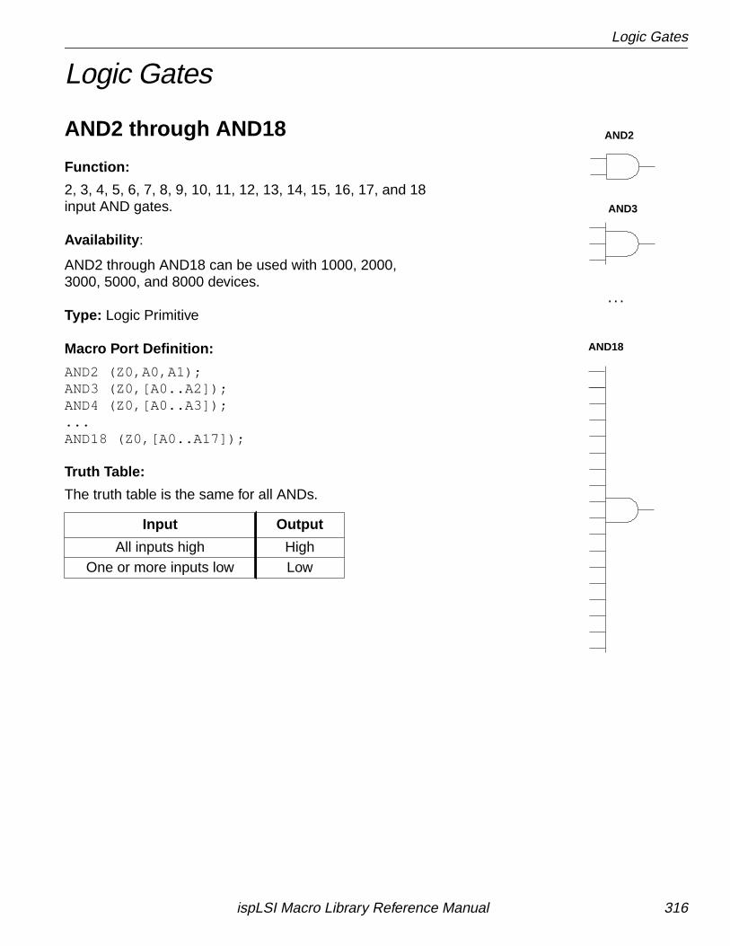
Logic Gates
Logic Gates
AND2 through AND18
Function:
2, 3, 4, 5, 6, 7, 8, 9, 10, 11, 12, 13, 14, 15, 16, 17, and 18input AND gates.
Availability :
AND2 through AND18 can be used with 1000, 2000,3000, 5000, and 8000 devices.
Type: Logic Primitive
Macro Port Definition:
AND2 (Z0,A0,A1);AND3 (Z0,[A0..A2]);AND4 (Z0,[A0..A3]);...AND18 (Z0,[A0..A17]);
Truth Table:
The truth table is the same for all ANDs.
Input Output
All inputs high HighOne or more inputs low Low
AND2
AND3
AND18
. . .
ispLSI Macro Library Reference Manual 316
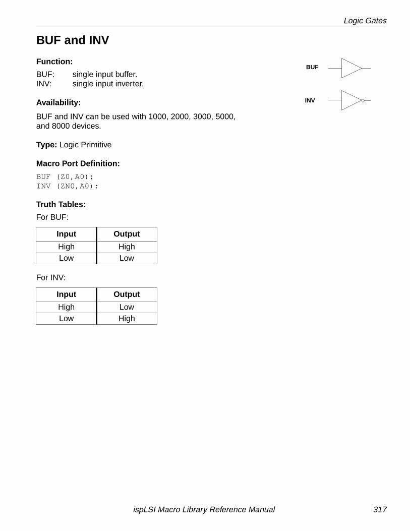
Logic Gates
BUF and INV
Function:
BUF: single input buffer.INV: single input inverter.
Availability:
BUF and INV can be used with 1000, 2000, 3000, 5000,and 8000 devices.
Type: Logic Primitive
Macro Port Definition:
BUF (Z0,A0);INV (ZN0,A0);
Truth Tables:
For BUF:
For INV:
Input Output
High HighLow Low
Input Output
High LowLow High
BUF
INV
ispLSI Macro Library Reference Manual 317
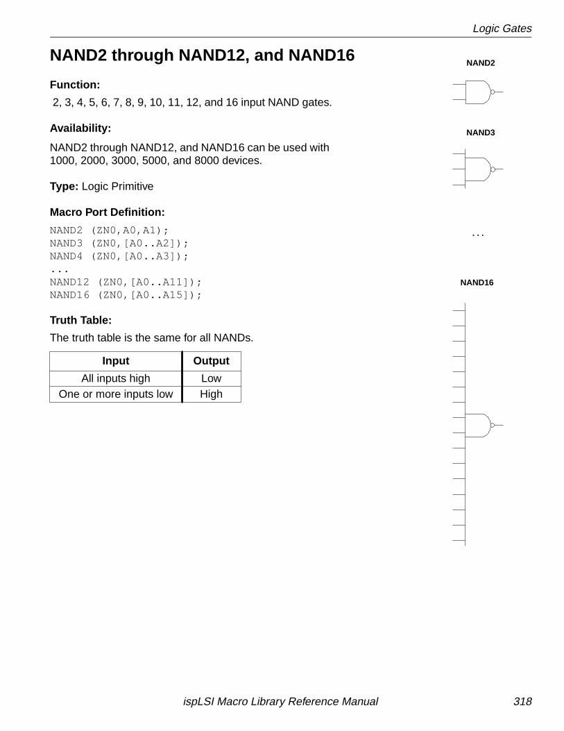
Logic Gates
NAND2 through NAND12, and NAND16
Function:
2, 3, 4, 5, 6, 7, 8, 9, 10, 11, 12, and 16 input NAND gates.
Availability:
NAND2 through NAND12, and NAND16 can be used with1000, 2000, 3000, 5000, and 8000 devices.
Type: Logic Primitive
Macro Port Definition:
NAND2 (ZN0,A0,A1);NAND3 (ZN0,[A0..A2]);NAND4 (ZN0,[A0..A3]);...NAND12 (ZN0,[A0..A11]);NAND16 (ZN0,[A0..A15]);
Truth Table:
The truth table is the same for all NANDs.
Input Output
All inputs high LowOne or more inputs low High
NAND2
NAND3
. . .
NAND16
ispLSI Macro Library Reference Manual 318
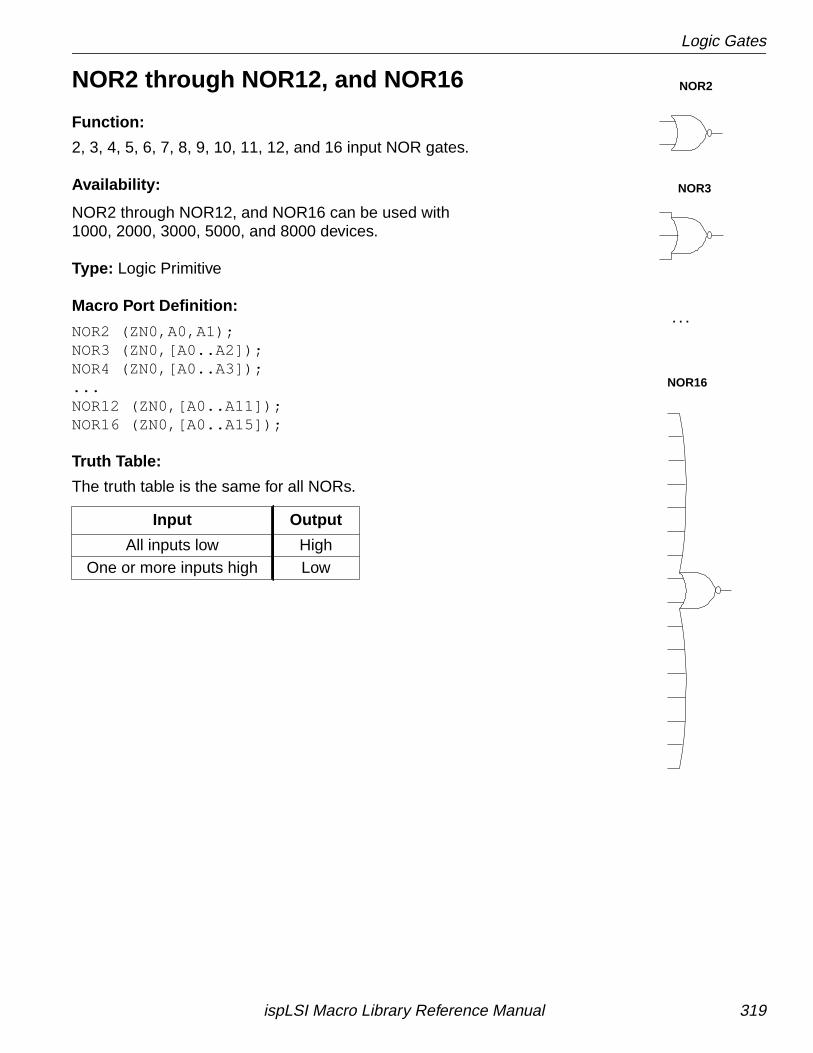
Logic Gates
NOR2 through NOR12, and NOR16
Function:
2, 3, 4, 5, 6, 7, 8, 9, 10, 11, 12, and 16 input NOR gates.
Availability:
NOR2 through NOR12, and NOR16 can be used with1000, 2000, 3000, 5000, and 8000 devices.
Type: Logic Primitive
Macro Port Definition:
NOR2 (ZN0,A0,A1);NOR3 (ZN0,[A0..A2]);NOR4 (ZN0,[A0..A3]);...NOR12 (ZN0,[A0..A11]);NOR16 (ZN0,[A0..A15]);
Truth Table:
The truth table is the same for all NORs.
Input Output
All inputs low HighOne or more inputs high Low
NOR2
NOR3
NOR16
. . .
ispLSI Macro Library Reference Manual 319
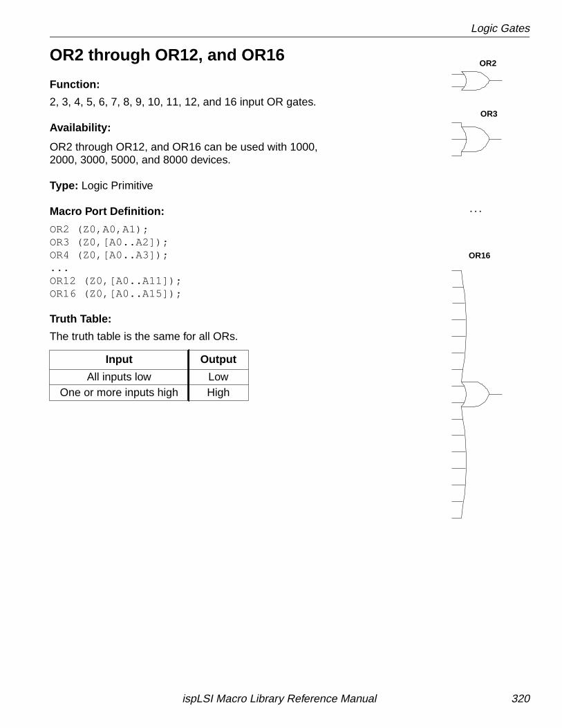
Logic Gates
OR2 through OR12, and OR16
Function:
2, 3, 4, 5, 6, 7, 8, 9, 10, 11, 12, and 16 input OR gates.
Availability:
OR2 through OR12, and OR16 can be used with 1000,2000, 3000, 5000, and 8000 devices.
Type: Logic Primitive
Macro Port Definition:
OR2 (Z0,A0,A1);OR3 (Z0,[A0..A2]);OR4 (Z0,[A0..A3]);...OR12 (Z0,[A0..A11]);OR16 (Z0,[A0..A15]);
Truth Table:
The truth table is the same for all ORs.
Input Output
All inputs low LowOne or more inputs high High
OR2
OR3
OR16
. . .
ispLSI Macro Library Reference Manual 320
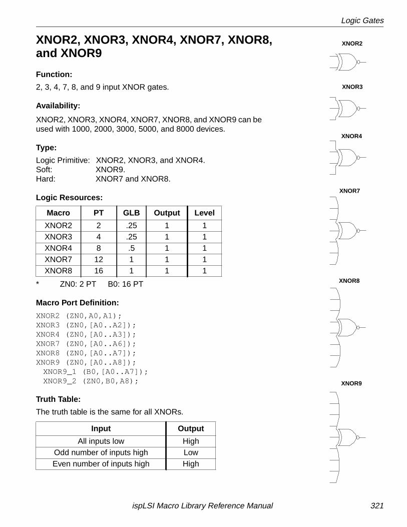
Logic Gates
XNOR2, XNOR3, XNOR4, XNOR7, XNOR8,and XNOR9
Function:
2, 3, 4, 7, 8, and 9 input XNOR gates.
Availability:
XNOR2, XNOR3, XNOR4, XNOR7, XNOR8, and XNOR9 can beused with 1000, 2000, 3000, 5000, and 8000 devices.
Type:
Logic Primitive: XNOR2, XNOR3, and XNOR4.Soft: XNOR9.Hard: XNOR7 and XNOR8.
Logic Resources:
* ZN0: 2 PT B0: 16 PT
Macro Port Definition:
XNOR2 (ZN0,A0,A1);XNOR3 (ZN0,[A0..A2]);XNOR4 (ZN0,[A0..A3]);XNOR7 (ZN0,[A0..A6]);XNOR8 (ZN0,[A0..A7]);XNOR9 (ZN0,[A0..A8]);
XNOR9_1 (B0,[A0..A7]);XNOR9_2 (ZN0,B0,A8);
Truth Table:
The truth table is the same for all XNORs.
Macro PT GLB Output Level
XNOR2 2 .25 1 1XNOR3 4 .25 1 1XNOR4 8 .5 1 1XNOR7 12 1 1 1XNOR8 16 1 1 1
Input Output
All inputs low HighOdd number of inputs high LowEven number of inputs high High
XNOR2
XNOR3
XNOR4
XNOR8
XNOR9
XNOR7
ispLSI Macro Library Reference Manual 321
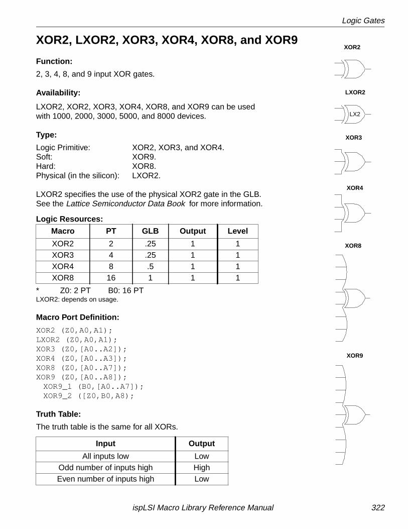
Logic Gates
XOR2, LXOR2, XOR3, XOR4, XOR8, and XOR9
Function:
2, 3, 4, 8, and 9 input XOR gates.
Availability:
LXOR2, XOR2, XOR3, XOR4, XOR8, and XOR9 can be usedwith 1000, 2000, 3000, 5000, and 8000 devices.
Type:
Logic Primitive: XOR2, XOR3, and XOR4.Soft: XOR9.Hard: XOR8.Physical (in the silicon): LXOR2.
LXOR2 specifies the use of the physical XOR2 gate in the GLB.See the Lattice Semiconductor Data Book for more information.
Logic Resources:
* Z0: 2 PT B0: 16 PTLXOR2: depends on usage.
Macro Port Definition:
XOR2 (Z0,A0,A1);LXOR2 (Z0,A0,A1);XOR3 (Z0,[A0..A2]);XOR4 (Z0,[A0..A3]);XOR8 (Z0,[A0..A7]);XOR9 (Z0,[A0..A8]);
XOR9_1 (B0,[A0..A7]);XOR9_2 ([Z0,B0,A8);
Truth Table:
The truth table is the same for all XORs.
Macro PT GLB Output Level
XOR2 2 .25 1 1XOR3 4 .25 1 1XOR4 8 .5 1 1XOR8 16 1 1 1
Input Output
All inputs low LowOdd number of inputs high HighEven number of inputs high Low
XOR2
XOR3
XOR4
XOR8
XOR9
LXOR2
LX2
ispLSI Macro Library Reference Manual 322
MUX/DMUX
This chapter contains information on the following macros:
■ Multiplexers
■ Demultiplexers
ispLSI Macro Library Reference Manual 323
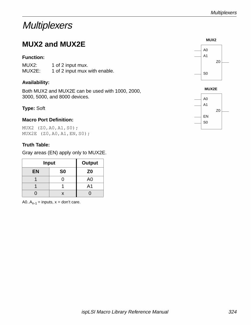
Multiplexers
Multiplexers
MUX2 and MUX2E
Function:
MUX2: 1 of 2 input mux.MUX2E: 1 of 2 input mux with enable.
Availability:
Both MUX2 and MUX2E can be used with 1000, 2000,3000, 5000, and 8000 devices.
Type: Soft
Macro Port Definition:
MUX2 (Z0,A0,A1,S0);MUX2E (Z0,A0,A1,EN,S0);
Truth Table:
Gray areas (EN) apply only to MUX2E.
A0..An-1 = inputs, x = don’t care.
Input Output
EN S0 Z0
1 0 A01 1 A10 x 0
Z0
S0
A1
A0
Z0
S0
EN
A1
A0
MUX2
MUX2E
ispLSI Macro Library Reference Manual 324
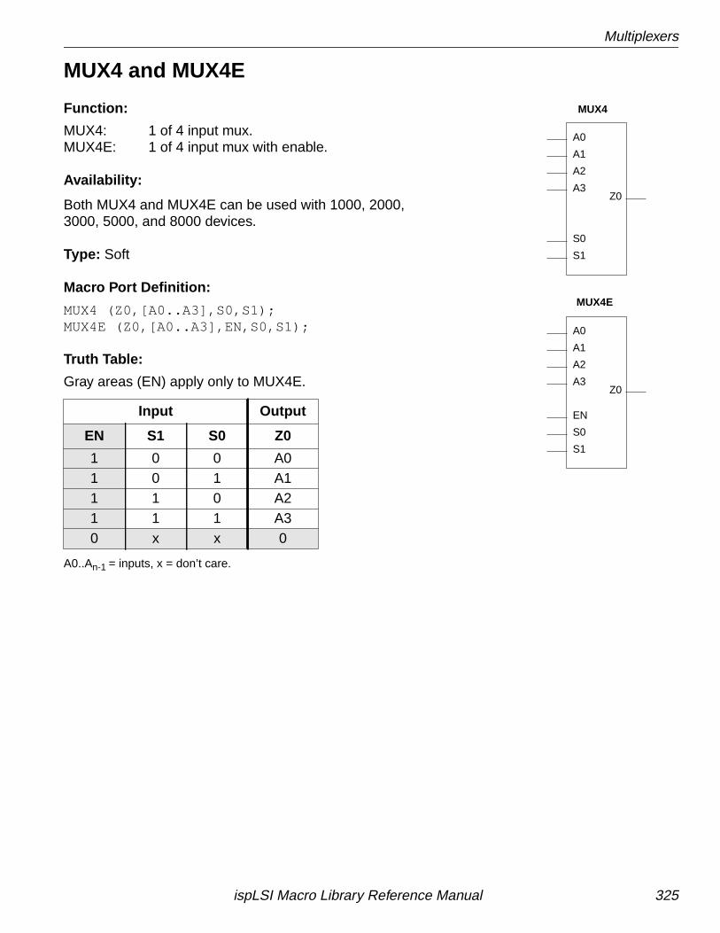
Multiplexers
MUX4 and MUX4E
Function:
MUX4: 1 of 4 input mux.MUX4E: 1 of 4 input mux with enable.
Availability:
Both MUX4 and MUX4E can be used with 1000, 2000,3000, 5000, and 8000 devices.
Type: Soft
Macro Port Definition:
MUX4 (Z0,[A0..A3],S0,S1);MUX4E (Z0,[A0..A3],EN,S0,S1);
Truth Table:
Gray areas (EN) apply only to MUX4E.
A0..An-1 = inputs, x = don’t care.
Input Output
EN S1 S0 Z0
1 0 0 A01 0 1 A11 1 0 A21 1 1 A30 x x 0
Z0
EN
S1
S0
A3
A2
A1
A0
MUX4
MUX4E
Z0
S1
S0
A3
A2
A1
A0
ispLSI Macro Library Reference Manual 325
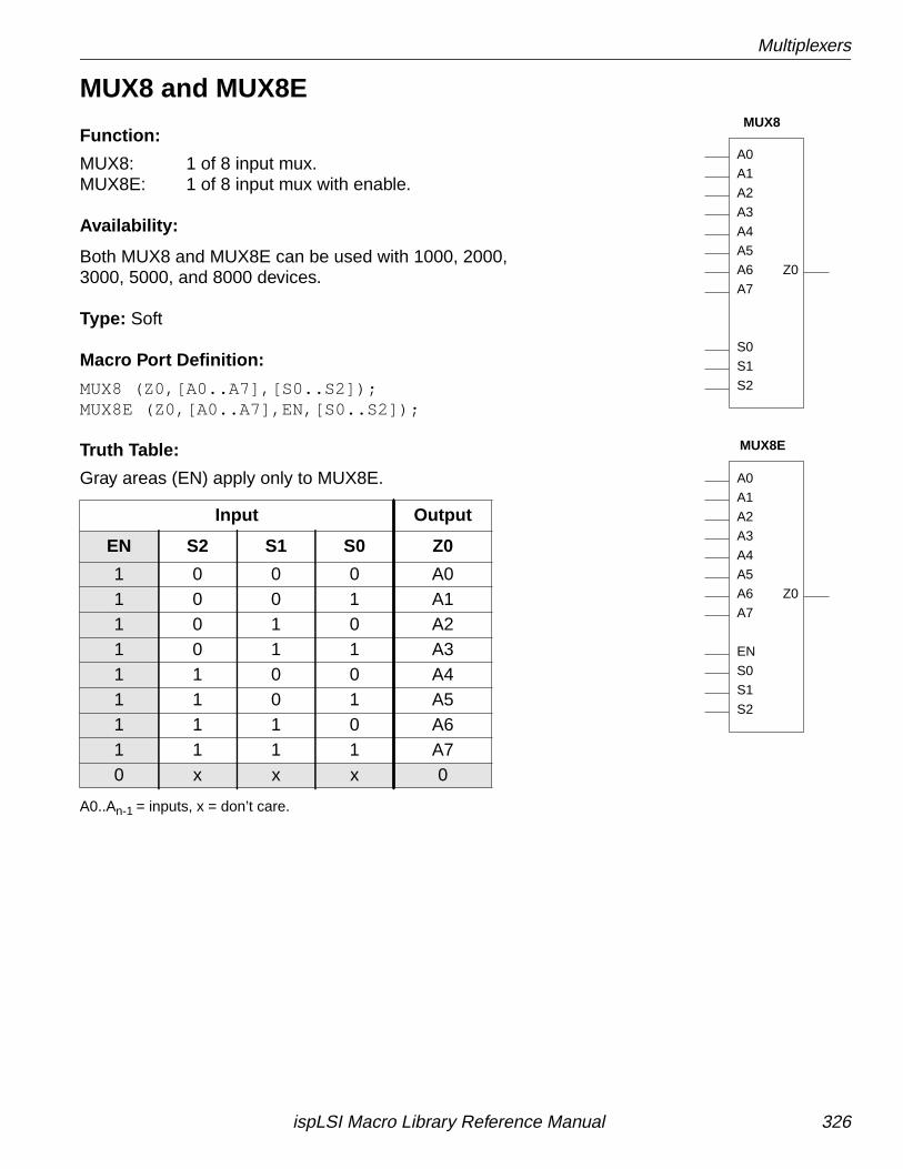
Multiplexers
MUX8 and MUX8E
Function:
MUX8: 1 of 8 input mux.MUX8E: 1 of 8 input mux with enable.
Availability:
Both MUX8 and MUX8E can be used with 1000, 2000,3000, 5000, and 8000 devices.
Type: Soft
Macro Port Definition:
MUX8 (Z0,[A0..A7],[S0..S2]);MUX8E (Z0,[A0..A7],EN,[S0..S2]);
Truth Table:
Gray areas (EN) apply only to MUX8E.
A0..An-1 = inputs, x = don’t care.
Input Output
EN S2 S1 S0 Z0
1 0 0 0 A01 0 0 1 A11 0 1 0 A21 0 1 1 A31 1 0 0 A41 1 0 1 A51 1 1 0 A61 1 1 1 A70 x x x 0
MUX8
MUX8E
Z0
S0
S2
S1
EN
A7
A6
A5A4
A3
A2
A1A0
Z0
S0
S2
S1
A7
A6
A5A4
A3
A2
A1A0
ispLSI Macro Library Reference Manual 326
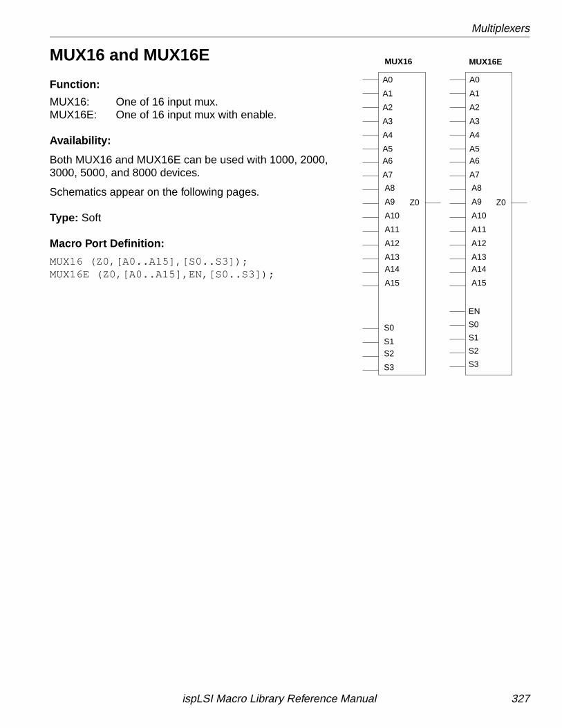
Multiplexers
MUX16 and MUX16E
Function:
MUX16: One of 16 input mux.MUX16E: One of 16 input mux with enable.
Availability:
Both MUX16 and MUX16E can be used with 1000, 2000,3000, 5000, and 8000 devices.
Schematics appear on the following pages.
Type: Soft
Macro Port Definition:
MUX16 (Z0,[A0..A15],[S0..S3]);MUX16E (Z0,[A0..A15],EN,[S0..S3]);
MUX16 MUX16E
A5
A1
A0
A3
A2
A4
Z0
A7
A6
A13
A9
A8
A11
A10
A12
A15
A14
S1
S0
S3
S2
A5
A1
A0
A3
A2
A4
Z0
A7
A6
A13
A9
A8
A11
A10
A12
A15
A14
S1
S0
S3
S2
EN
ispLSI Macro Library Reference Manual 327
Multiplexers
Truth Table:
Gray areas (EN) apply only to MUX16E.
A0..An-1 = inputs, x = don’t care.
Input Output
EN S3 S2 S1 S0 Z0
1 0 0 0 0 A01 0 0 0 1 A11 0 0 1 0 A21 0 0 1 1 A31 0 1 0 0 A41 0 1 0 1 A51 0 1 1 0 A61 0 1 1 1 A71 1 0 0 0 A81 1 0 0 1 A91 1 0 1 0 A101 1 0 1 1 A111 1 1 0 0 A121 1 1 0 1 A131 1 1 1 0 A141 1 1 1 1 A150 x x x x 0
ispLSI Macro Library Reference Manual 328
Multiplexers
S3
A15
A14
A13
A12
A11
A10
A9
S1
S0
S2
A0
A1
A2
A3
A4
A5
A6
Z0
A7
A8
MUX16
ispLSI Macro Library Reference Manual 329
Multiplexers
Z0
A7
A6
A5
A4
A3
A2
A1
A0
A8
A9
A10
A11
A12
A13
A14
MUX16E
ispLSI Macro Library Reference Manual 330
Multiplexers
MUX22 and MUX22E
Function:
MUX22: Dual 1 of 2 input mux with common select line.MUX22E: Dual 1 of 2 input mux with common select line and
enable.
Availability:
Both MUX22 and MUX22E can be used with 1000, 2000,3000, 5000, and 8000 devices.
Type: Soft
Macro Port Definition:
MUX22 (Z0,Z1,A0,A1,B0,B1,S0);MUX22E (Z0,Z1,A0,A1,B0,B1,EN,S0);
Truth Table:
Gray areas (EN) apply only to MUX22E.
A0..An-1 = inputs, B0..Bn-1 = inputs,x = don’t care.
Input Output
EN S0 Z0 Z1
1 0 A0 A11 1 B0 B10 x 0 0
MUX22
MUX22E
B0
EN
S0
B1
A0
A1
Z1
Z0
B0
S0
B1
A0
A1
Z1
Z0
ispLSI Macro Library Reference Manual 331
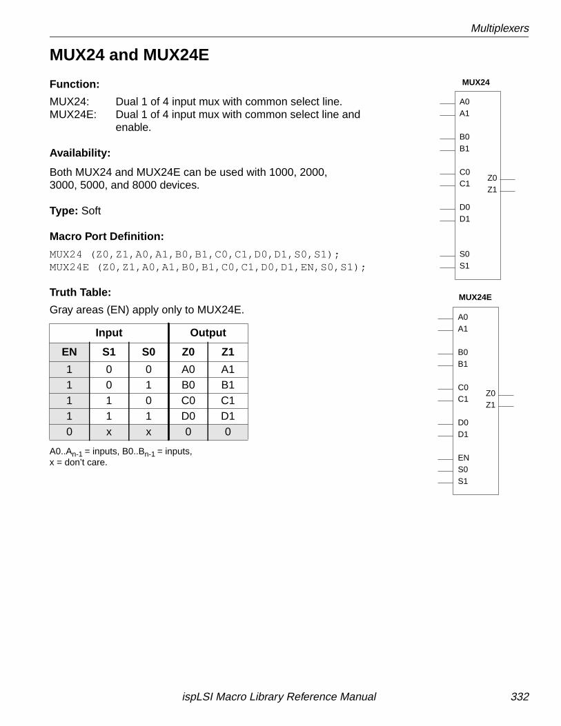
Multiplexers
MUX24 and MUX24E
Function:
MUX24: Dual 1 of 4 input mux with common select line.MUX24E: Dual 1 of 4 input mux with common select line and
enable.
Availability:
Both MUX24 and MUX24E can be used with 1000, 2000,3000, 5000, and 8000 devices.
Type: Soft
Macro Port Definition:
MUX24 (Z0,Z1,A0,A1,B0,B1,C0,C1,D0,D1,S0,S1);MUX24E (Z0,Z1,A0,A1,B0,B1,C0,C1,D0,D1,EN,S0,S1);
Truth Table:
Gray areas (EN) apply only to MUX24E.
A0..An-1 = inputs, B0..Bn-1 = inputs,x = don’t care.
Input Output
EN S1 S0 Z0 Z1
1 0 0 A0 A11 0 1 B0 B11 1 0 C0 C11 1 1 D0 D10 x x 0 0
MUX24
MUX24E
Z0Z1
S0
A0A1
B0B1
C0C1
D0D1
EN
S1
Z0Z1
S0
A0A1
B0B1
C0C1
D0D1
S1
ispLSI Macro Library Reference Manual 332
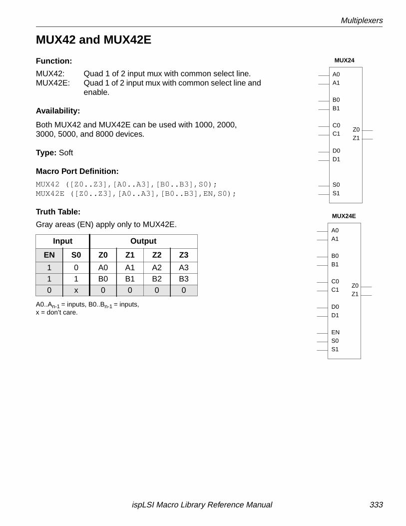
Multiplexers
MUX42 and MUX42E
Function:
MUX42: Quad 1 of 2 input mux with common select line.MUX42E: Quad 1 of 2 input mux with common select line and
enable.
Availability:
Both MUX42 and MUX42E can be used with 1000, 2000,3000, 5000, and 8000 devices.
Type: Soft
Macro Port Definition:
MUX42 ([Z0..Z3],[A0..A3],[B0..B3],S0);MUX42E ([Z0..Z3],[A0..A3],[B0..B3],EN,S0);
Truth Table:
Gray areas (EN) apply only to MUX42E.
A0..An-1 = inputs, B0..Bn-1 = inputs,x = don’t care.
Input Output
EN S0 Z0 Z1 Z2 Z3
1 0 A0 A1 A2 A31 1 B0 B1 B2 B30 x 0 0 0 0
MUX24
MUX24E
Z0Z1
S0
A0A1
B0B1
C0C1
D0D1
EN
S1
Z0Z1
S0
A0A1
B0B1
C0C1
D0D1
S1
ispLSI Macro Library Reference Manual 333
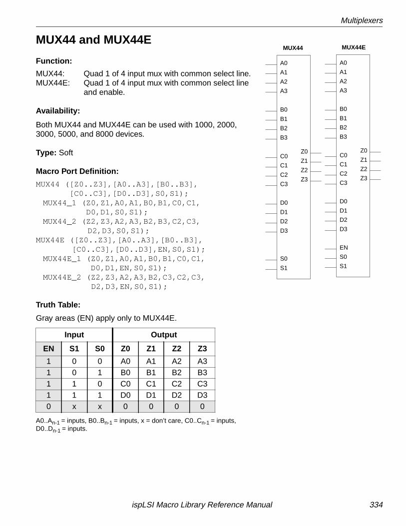
Multiplexers
MUX44 and MUX44E
Function:
MUX44: Quad 1 of 4 input mux with common select line.MUX44E: Quad 1 of 4 input mux with common select line
and enable.
Availability:
Both MUX44 and MUX44E can be used with 1000, 2000,3000, 5000, and 8000 devices.
Type: Soft
Macro Port Definition:
MUX44 ([Z0..Z3],[A0..A3],[B0..B3],[C0..C3],[D0..D3],S0,S1);
MUX44_1 (Z0,Z1,A0,A1,B0,B1,C0,C1, D0,D1,S0,S1);MUX44_2 (Z2,Z3,A2,A3,B2,B3,C2,C3,
D2,D3,S0,S1);MUX44E ([Z0..Z3],[A0..A3],[B0..B3],
[C0..C3],[D0..D3],EN,S0,S1);MUX44E_1 (Z0,Z1,A0,A1,B0,B1,C0,C1, D0,D1,EN,S0,S1);MUX44E_2 (Z2,Z3,A2,A3,B2,C3,C2,C3,
D2,D3,EN,S0,S1);
Truth Table:
Gray areas (EN) apply only to MUX44E.
A0..An-1 = inputs, B0..Bn-1 = inputs, x = don’t care, C0..Cn-1 = inputs,D0..Dn-1 = inputs.
Input Output
EN S1 S0 Z0 Z1 Z2 Z3
1 0 0 A0 A1 A2 A31 0 1 B0 B1 B2 B31 1 0 C0 C1 C2 C31 1 1 D0 D1 D2 D30 x x 0 0 0 0
MUX44 MUX44E
Z0
Z1
Z2
Z3
EN
S1
A0
A1
A2
A3
B0
B1
B2
B3
S0
D3
D2
C3
C2
C1
C0
D1
D0
Z0
Z1
Z2
Z3
S1
A0
A1
A2
A3
B0
B1
B2
B3
S0
D3
D2
C3
C2
C1
C0
D1
D0
ispLSI Macro Library Reference Manual 334
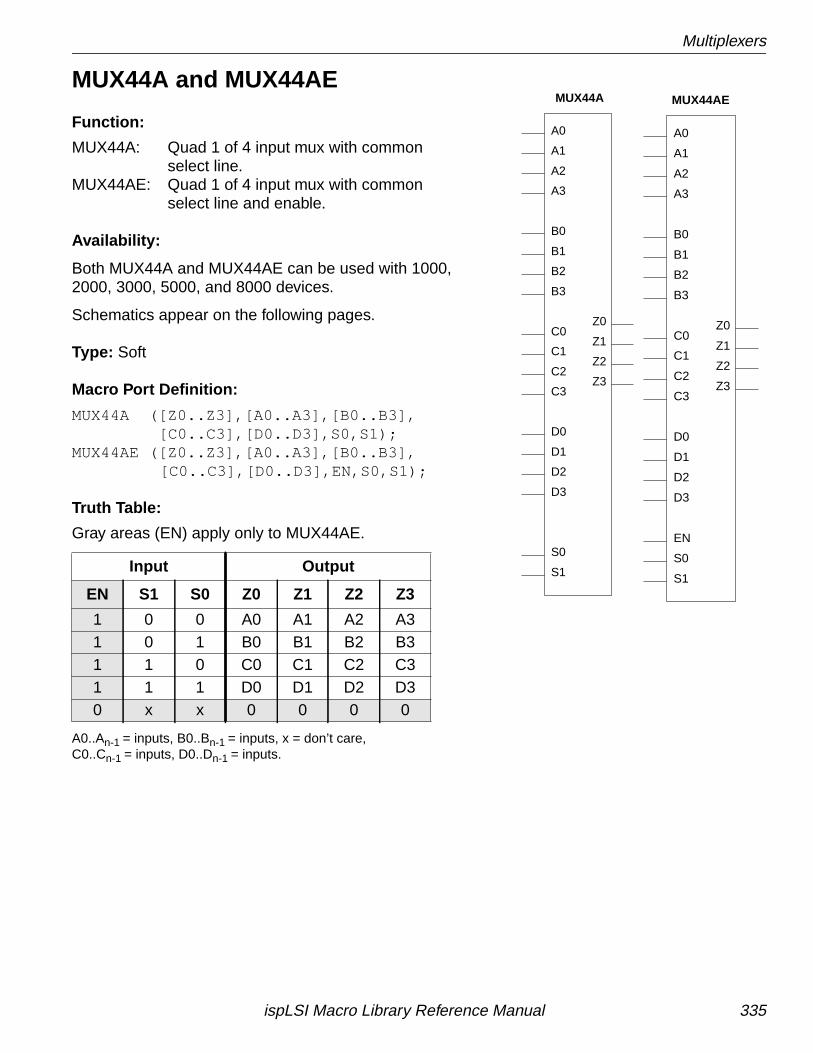
Multiplexers
MUX44A and MUX44AE
Function:
MUX44A: Quad 1 of 4 input mux with commonselect line.
MUX44AE: Quad 1 of 4 input mux with commonselect line and enable.
Availability:
Both MUX44A and MUX44AE can be used with 1000,2000, 3000, 5000, and 8000 devices.
Schematics appear on the following pages.
Type: Soft
Macro Port Definition:
MUX44A ([Z0..Z3],[A0..A3],[B0..B3],[C0..C3],[D0..D3],S0,S1);
MUX44AE ([Z0..Z3],[A0..A3],[B0..B3],[C0..C3],[D0..D3],EN,S0,S1);
Truth Table:
Gray areas (EN) apply only to MUX44AE.
A0..An-1 = inputs, B0..Bn-1 = inputs, x = don’t care,C0..Cn-1 = inputs, D0..Dn-1 = inputs.
Input Output
EN S1 S0 Z0 Z1 Z2 Z3
1 0 0 A0 A1 A2 A31 0 1 B0 B1 B2 B31 1 0 C0 C1 C2 C31 1 1 D0 D1 D2 D30 x x 0 0 0 0
MUX44A MUX44AE
Z0
Z1
Z2
Z3
EN
S1
A0
A1
A2
A3
B0
B1
B2
B3
S0
D3
D2
C3
C2
C1
C0
D1
D0
Z0
Z1
Z2
Z3
S1
A0
A1
A2
A3
B0
B1
B2
B3
S0
D3
D2
C3
C2
C1
C0
D1
D0
ispLSI Macro Library Reference Manual 335
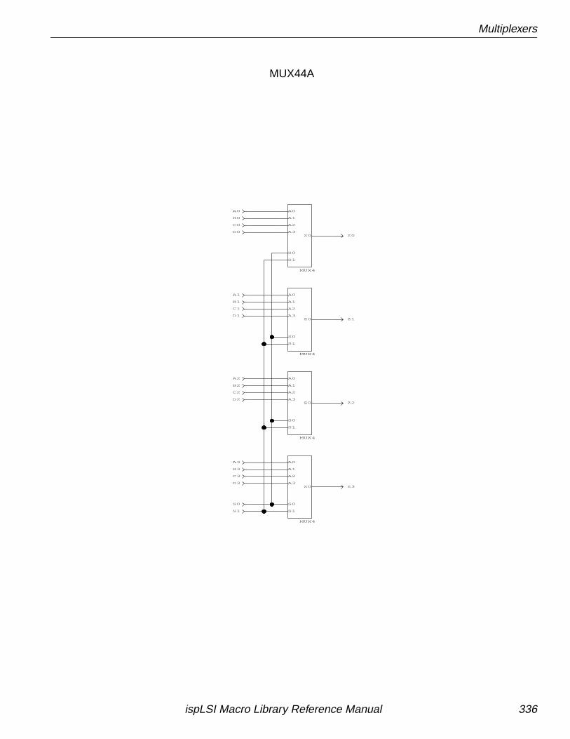
Multiplexers
S0
D3
A2
A3
C3
B3
B0
C0
Z0
A0
A1
A2
A3
S0
S1
MUX4
Z0
A0
A1
A2
A3
S0
S1
MUX4
D2
S1
Z3
Z2
Z0
Z1D1
C1
B1
A1
A0
D0
Z0
A0
A1
A2
A3
S0
S1
MUX4
Z0
A0
A1
A2
A3
S0
S1
MUX4
B2
C2
MUX44A
ispLSI Macro Library Reference Manual 336
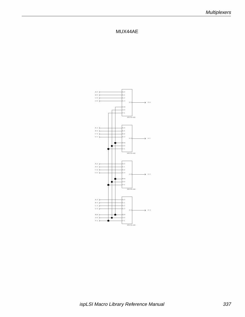
Multiplexers
Z3
Z2
Z1
Z0
A0
B0
C0
D0
A1
B1
C1
D1
A2
B2
C2
D2
A3
B3
C3
D3
EN
S0
S1
Z0
EN
S1
S0
A3
A2
A1
A0
MUX4E
Z0
EN
S1
S0
A3
A2
A1
A0
MUX4E
Z0
EN
S1
S0
A3
A2
A1
A0
MUX4E
Z0
EN
S1
S0
A3
A2
A1
A0
MUX4E
MUX44AE
ispLSI Macro Library Reference Manual 337
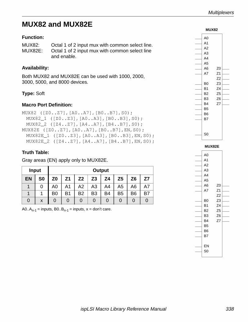
Multiplexers
MUX82 and MUX82E
Function:
MUX82: Octal 1 of 2 input mux with common select line.MUX82E: Octal 1 of 2 input mux with common select line
and enable.
Availability:
Both MUX82 and MUX82E can be used with 1000, 2000,3000, 5000, and 8000 devices.
Type: Soft
Macro Port Definition:
MUX82 ([Z0..Z7],[A0..A7],[B0..B7],S0);MUX82_1 ([Z0..Z3],[A0..A3],[B0..B3],S0);MUX82_2 ([Z4..Z7],[A4..A7],[B4..B7],S0);
MUX82E ([Z0..Z7],[A0..A7],[B0..B7],EN,S0);MUX82E_1 ([Z0..Z3],[A0..A3],[B0..B3],EN,S0);MUX82E_2 ([Z4..Z7],[A4..A7],[B4..B7],EN,S0);
Truth Table:
Gray areas (EN) apply only to MUX82E.
A0..An-1 = inputs, B0..Bn-1 = inputs, x = don’t care.
Input Output
EN S0 Z0 Z1 Z2 Z3 Z4 Z5 Z6 Z7
1 0 A0 A1 A2 A3 A4 A5 A6 A71 1 B0 B1 B2 B3 B4 B5 B6 B70 x 0 0 0 0 0 0 0 0
MUX82
MUX82E
Z0Z1Z2Z3Z4Z5Z6Z7
A4A5A6A7
B0B1B2B3B4B5B6B7
A0A1A2A3
ENS0
Z0Z1Z2Z3Z4Z5Z6Z7
A4A5A6A7
B0B1B2B3B4B5B6B7
A0A1A2A3
S0
ispLSI Macro Library Reference Manual 338
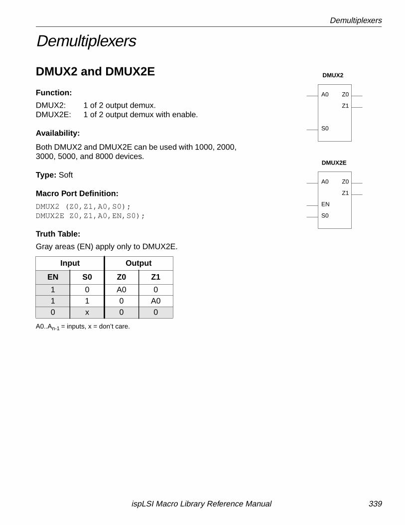
Demultiplexers
Demultiplexers
DMUX2 and DMUX2E
Function:
DMUX2: 1 of 2 output demux.DMUX2E: 1 of 2 output demux with enable.
Availability:
Both DMUX2 and DMUX2E can be used with 1000, 2000,3000, 5000, and 8000 devices.
Type: Soft
Macro Port Definition:
DMUX2 (Z0,Z1,A0,S0);DMUX2E Z0,Z1,A0,EN,S0);
Truth Table:
Gray areas (EN) apply only to DMUX2E.
A0..An-1 = inputs, x = don’t care.
Input Output
EN S0 Z0 Z1
1 0 A0 01 1 0 A00 x 0 0
Z1
Z0A0
EN
S0
DMUX2
DMUX2E
Z1
Z0A0
S0
ispLSI Macro Library Reference Manual 339
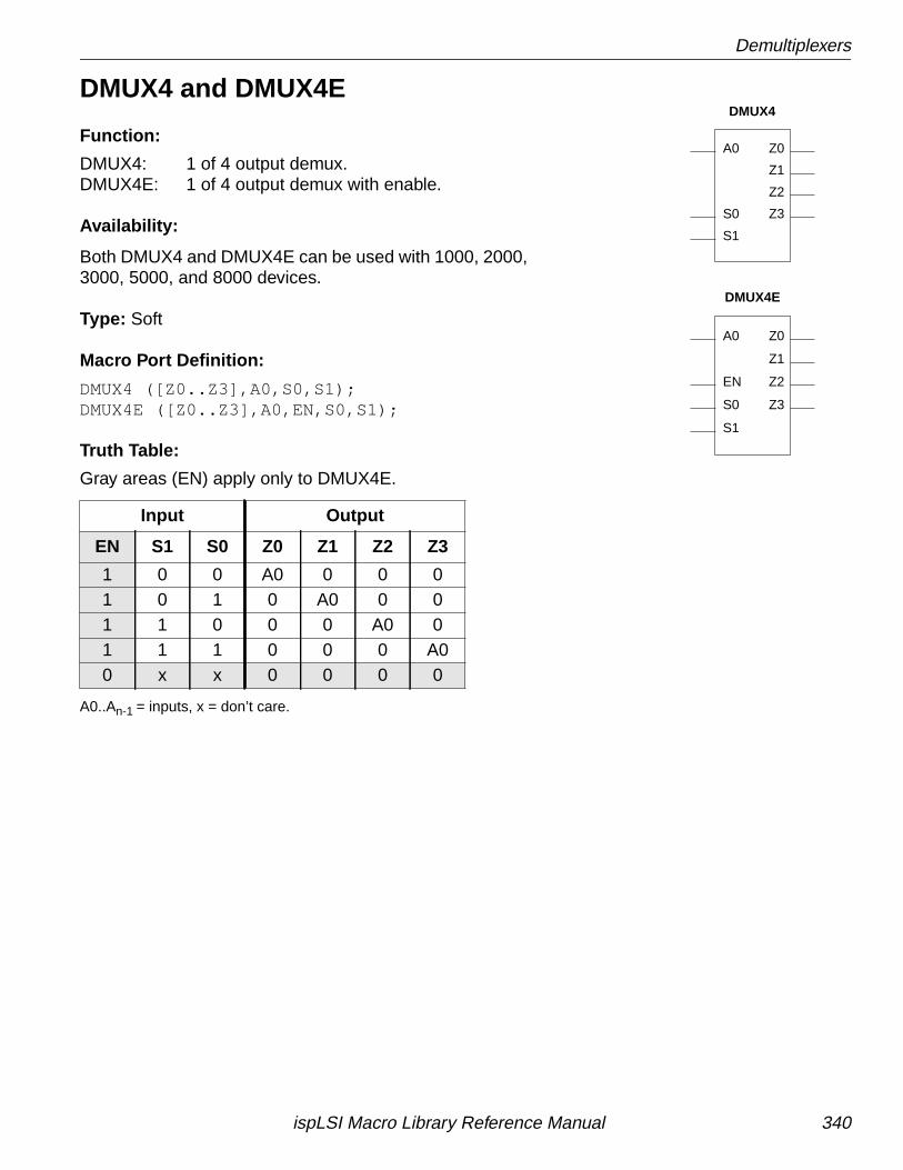
Demultiplexers
DMUX4 and DMUX4E
Function:
DMUX4: 1 of 4 output demux.DMUX4E: 1 of 4 output demux with enable.
Availability:
Both DMUX4 and DMUX4E can be used with 1000, 2000,3000, 5000, and 8000 devices.
Type: Soft
Macro Port Definition:
DMUX4 ([Z0..Z3],A0,S0,S1);DMUX4E ([Z0..Z3],A0,EN,S0,S1);
Truth Table:
Gray areas (EN) apply only to DMUX4E.
A0..An-1 = inputs, x = don’t care.
Input Output
EN S1 S0 Z0 Z1 Z2 Z3
1 0 0 A0 0 0 01 0 1 0 A0 0 01 1 0 0 0 A0 01 1 1 0 0 0 A00 x x 0 0 0 0
DMUX4
DMUX4E
Z3
Z2
Z1
Z0A0
EN
S0
S1
Z3
Z2
Z1
Z0A0
S0
S1
ispLSI Macro Library Reference Manual 340
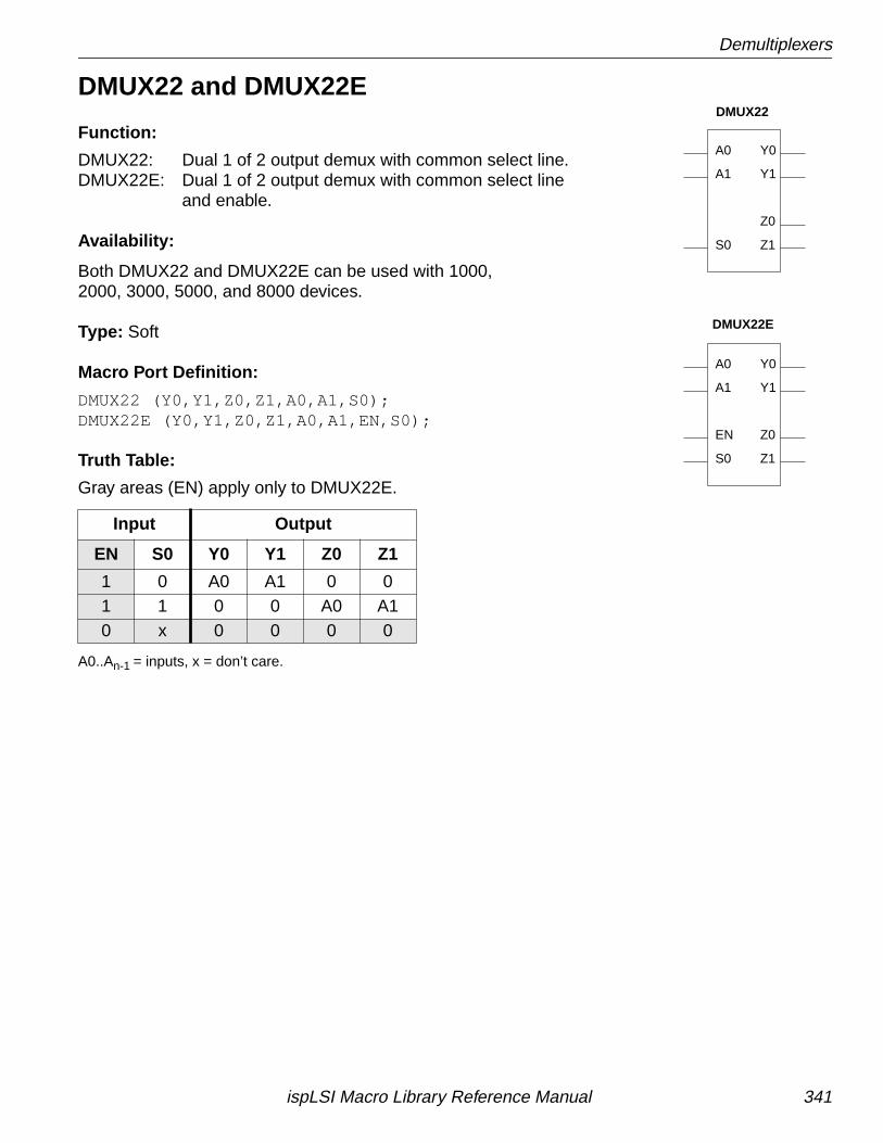
Demultiplexers
DMUX22 and DMUX22E
Function:
DMUX22: Dual 1 of 2 output demux with common select line.DMUX22E: Dual 1 of 2 output demux with common select line
and enable.
Availability:
Both DMUX22 and DMUX22E can be used with 1000,2000, 3000, 5000, and 8000 devices.
Type: Soft
Macro Port Definition:
DMUX22 (Y0,Y1,Z0,Z1,A0,A1,S0);DMUX22E (Y0,Y1,Z0,Z1,A0,A1,EN,S0);
Truth Table:
Gray areas (EN) apply only to DMUX22E.
A0..An-1 = inputs, x = don’t care.
Input Output
EN S0 Y0 Y1 Z0 Z1
1 0 A0 A1 0 01 1 0 0 A0 A10 x 0 0 0 0
DMUX22
DMUX22E
S0
A0
EN
A1 Y1
Y0
Z0
Z1
S0
A0
A1 Y1
Y0
Z0
Z1
ispLSI Macro Library Reference Manual 341
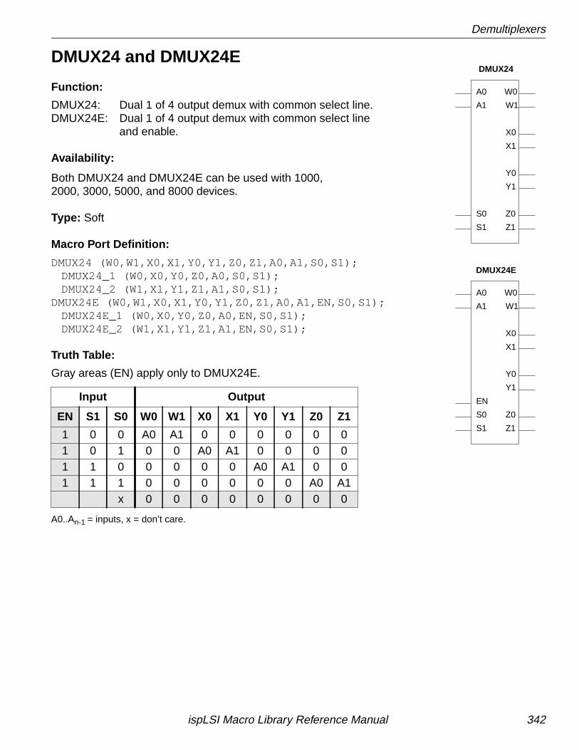
Demultiplexers
DMUX24 and DMUX24E
Function:
DMUX24: Dual 1 of 4 output demux with common select line.DMUX24E: Dual 1 of 4 output demux with common select line
and enable.
Availability:
Both DMUX24 and DMUX24E can be used with 1000,2000, 3000, 5000, and 8000 devices.
Type: Soft
Macro Port Definition:
DMUX24 (W0,W1,X0,X1,Y0,Y1,Z0,Z1,A0,A1,S0,S1);DMUX24_1 (W0,X0,Y0,Z0,A0,S0,S1);DMUX24_2 (W1,X1,Y1,Z1,A1,S0,S1);
DMUX24E (W0,W1,X0,X1,Y0,Y1,Z0,Z1,A0,A1,EN,S0,S1);DMUX24E_1 (W0,X0,Y0,Z0,A0,EN,S0,S1);DMUX24E_2 (W1,X1,Y1,Z1,A1,EN,S0,S1);
Truth Table:
Gray areas (EN) apply only to DMUX24E.
A0..An-1 = inputs, x = don’t care.
Input Output
EN S1 S0 W0 W1 X0 X1 Y0 Y1 Z0 Z1
1 0 0 A0 A1 0 0 0 0 0 01 0 1 0 0 A0 A1 0 0 0 01 1 0 0 0 0 0 A0 A1 0 01 1 1 0 0 0 0 0 0 A0 A1
x 0 0 0 0 0 0 0 0
DMUX24
DMUX24E
Z1
Z0
Y0
Y1
A0
A1
EN
S0
X1
X0
W1
W0
S1
Z1
Z0
Y0
Y1
A0
A1
S0
X1
X0
W1
W0
S1
ispLSI Macro Library Reference Manual 342
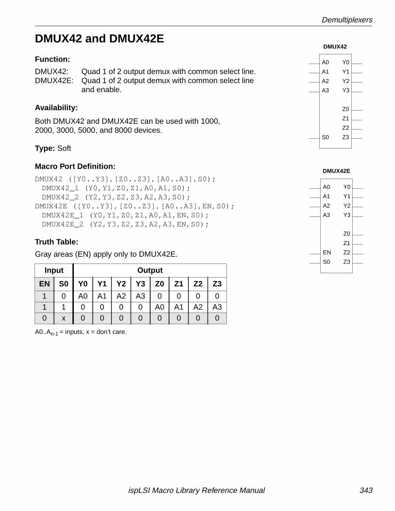
Demultiplexers
DMUX42 and DMUX42E
Function:
DMUX42: Quad 1 of 2 output demux with common select line.DMUX42E: Quad 1 of 2 output demux with common select line
and enable.
Availability:
Both DMUX42 and DMUX42E can be used with 1000,2000, 3000, 5000, and 8000 devices.
Type: Soft
Macro Port Definition:
DMUX42 ([Y0..Y3],[Z0..Z3],[A0..A3],S0);DMUX42_1 (Y0,Y1,Z0,Z1,A0,A1,S0);DMUX42_2 (Y2,Y3,Z2,Z3,A2,A3,S0);
DMUX42E ([Y0..Y3],[Z0..Z3],[A0..A3],EN,S0);DMUX42E_1 (Y0,Y1,Z0,Z1,A0,A1,EN,S0);DMUX42E_2 (Y2,Y3,Z2,Z3,A2,A3,EN,S0);
Truth Table:
Gray areas (EN) apply only to DMUX42E.
A0..An-1 = inputs, x = don’t care.
Input Output
EN S0 Y0 Y1 Y2 Y3 Z0 Z1 Z2 Z3
1 0 A0 A1 A2 A3 0 0 0 01 1 0 0 0 0 A0 A1 A2 A30 x 0 0 0 0 0 0 0 0
DMUX42
DMUX42E
S0
EN
A0
A1
Z3
Z2
Z1
Z0
Y3
Y2
Y1
Y0
A3
A2
S0
A0
A1
Z3
Z2
Z1
Z0
Y3
Y2
Y1
Y0
A3
A2
ispLSI Macro Library Reference Manual 343
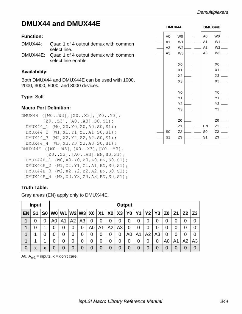
Demultiplexers
DMUX44 and DMUX44E
Function:
DMUX44: Quad 1 of 4 output demux with commonselect line.
DMUX44E: Quad 1 of 4 output demux with commonselect line enable.
Availability:
Both DMUX44 and DMUX44E can be used with 1000,2000, 3000, 5000, and 8000 devices.
Type: Soft
Macro Port Definition:
DMUX44 ([W0..W3],[X0..X3],[Y0..Y3], [Z0..Z3],[A0..A3],S0,S1);DMUX44_1 (W0,X0,Y0,Z0,A0,S0,S1);DMUX44_2 (W1,X1,Y1,Z1,A1,S0,S1);DMUX44_3 (W2,X2,Y2,Z2,A2,S0,S1);DMUX44_4 (W3,X3,Y3,Z3,A3,S0,S1);
DMUX44E ([W0..W3],[X0..X3],[Y0..Y3], [Z0..Z3],[A0..A3],EN,S0,S1);DMUX44E_1 (W0,X0,Y0,Z0,A0,EN,S0,S1);DMUX44E_2 (W1,X1,Y1,Z1,A1,EN,S0,S1);DMUX44E_3 (W2,X2,Y2,Z2,A2,EN,S0,S1);DMUX44E_4 (W3,X3,Y3,Z3,A3,EN,S0,S1);
Truth Table:
Gray areas (EN) apply only to DMUX44E.
A0..An-1 = inputs, x = don’t care.
Input Output
EN S1 S0 W0 W1 W2 W3 X0 X1 X2 X3 Y0 Y1 Y2 Y3 Z0 Z1 Z2 Z3
1 0 0 A0 A1 A2 A3 0 0 0 0 0 0 0 0 0 0 0 01 0 1 0 0 0 0 A0 A1 A2 A3 0 0 0 0 0 0 0 01 1 0 0 0 0 0 0 0 0 0 A0 A1 A2 A3 0 0 0 01 1 1 0 0 0 0 0 0 0 0 0 0 0 0 A0 A1 A2 A30 x x 0 0 0 0 0 0 0 0 0 0 0 0 0 0 0 0
DMUX44 DMUX44E
EN
Z3
Z2
Z1
Z0
Y3
Y2
Y1
Y0
A0
A1
A2
A3
S1
S0
X3
X2
X1
X0
W3
W2
W1
W0
Z3
Z2
Z1
Z0
Y3
Y2
Y1
Y0
A0
A1
A2
A3
S1
S0
X3
X2
X1
X0
W3
W2
W1
W0
ispLSI Macro Library Reference Manual 344
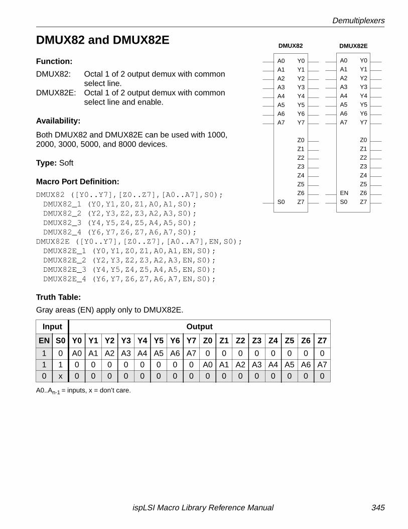
Demultiplexers
DMUX82 and DMUX82E
Function:
DMUX82: Octal 1 of 2 output demux with commonselect line.
DMUX82E: Octal 1 of 2 output demux with commonselect line and enable.
Availability:
Both DMUX82 and DMUX82E can be used with 1000,2000, 3000, 5000, and 8000 devices.
Type: Soft
Macro Port Definition:
DMUX82 ([Y0..Y7],[Z0..Z7],[A0..A7],S0);DMUX82_1 (Y0,Y1,Z0,Z1,A0,A1,S0);DMUX82_2 (Y2,Y3,Z2,Z3,A2,A3,S0);DMUX82_3 (Y4,Y5,Z4,Z5,A4,A5,S0);DMUX82_4 (Y6,Y7,Z6,Z7,A6,A7,S0);
DMUX82E ([Y0..Y7],[Z0..Z7],[A0..A7],EN,S0);DMUX82E_1 (Y0,Y1,Z0,Z1,A0,A1,EN,S0);DMUX82E_2 (Y2,Y3,Z2,Z3,A2,A3,EN,S0);DMUX82E_3 (Y4,Y5,Z4,Z5,A4,A5,EN,S0);DMUX82E_4 (Y6,Y7,Z6,Z7,A6,A7,EN,S0);
Truth Table:
Gray areas (EN) apply only to DMUX82E.
A0..An-1 = inputs, x = don’t care.
Input Output
EN S0 Y0 Y1 Y2 Y3 Y4 Y5 Y6 Y7 Z0 Z1 Z2 Z3 Z4 Z5 Z6 Z7
1 0 A0 A1 A2 A3 A4 A5 A6 A7 0 0 0 0 0 0 0 01 1 0 0 0 0 0 0 0 0 A0 A1 A2 A3 A4 A5 A6 A70 x 0 0 0 0 0 0 0 0 0 0 0 0 0 0 0 0
DMUX82 DMUX82E
Y0
Y1
Y2
Y3
Y4
Y5
Y6
Y7
Z0
Z1
Z2
Z3
Z4
Z5
Z6
Z7
A4
A5
A6
A7
A3
A2
A1
A0
EN
S0
Y0
Y1
Y2
Y3
Y4
Y5
Y6
Y7
Z0
Z1
Z2
Z3
Z4
Z5
Z6
Z7
A4
A5
A6
A7
A3
A2
A1
A0
S0
ispLSI Macro Library Reference Manual 345
Registers
This chapter contains information on the following macros:
■ D Flip-Flops
■ JK Flip-Flops
■ Toggle Flip-Flops
■ D Latches
■ SR Latches
■ Shift Registers
ispLSI Macro Library Reference Manual 346
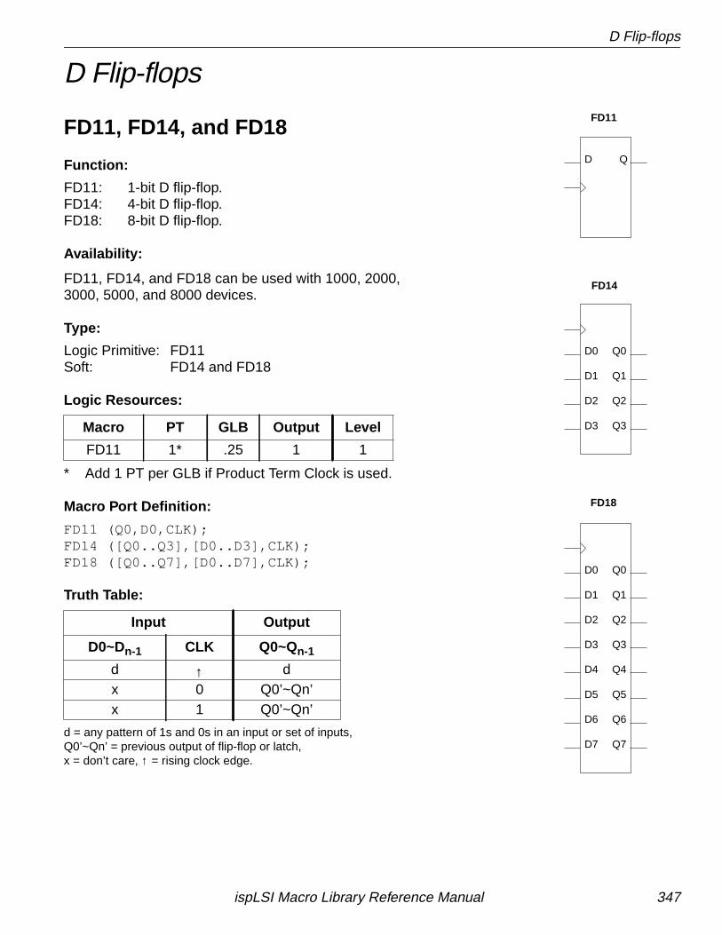
D Flip-flops
D Flip-flops
FD11, FD14, and FD18
Function:
FD11: 1-bit D flip-flop.FD14: 4-bit D flip-flop.FD18: 8-bit D flip-flop.
Availability:
FD11, FD14, and FD18 can be used with 1000, 2000,3000, 5000, and 8000 devices.
Type:
Logic Primitive: FD11Soft: FD14 and FD18
Logic Resources:
* Add 1 PT per GLB if Product Term Clock is used.
Macro Port Definition:
FD11 (Q0,D0,CLK);FD14 ([Q0..Q3],[D0..D3],CLK);FD18 ([Q0..Q7],[D0..D7],CLK);
Truth Table:
d = any pattern of 1s and 0s in an input or set of inputs,Q0’~Qn’ = previous output of flip-flop or latch,x = don’t care, ↑ = rising clock edge.
Macro PT GLB Output Level
FD11 1* .25 1 1
Input Output
D0~Dn-1 CLK Q0~Qn-1
d ↑ dx 0 Q0’~Qn’x 1 Q0’~Qn’
FD11
FD18
D Q
FD14
Q3
Q2
Q1
Q0D0
D1
D2
D3
Q3
Q2
Q1
Q0D0
D1
D2
D3
D7
D6
D5
D4 Q4
Q5
Q6
Q7
ispLSI Macro Library Reference Manual 347
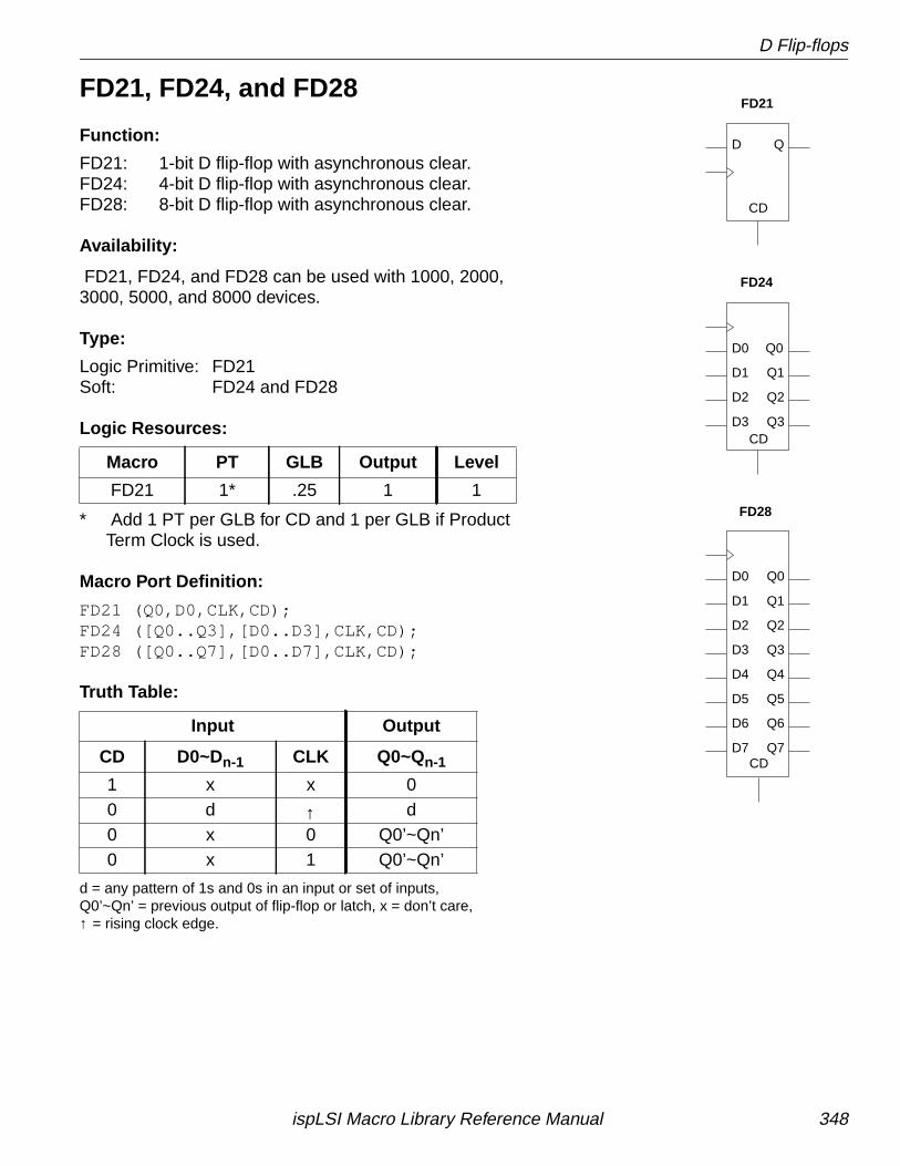
D Flip-flops
FD21, FD24, and FD28
Function:
FD21: 1-bit D flip-flop with asynchronous clear.FD24: 4-bit D flip-flop with asynchronous clear.FD28: 8-bit D flip-flop with asynchronous clear.
Availability:
FD21, FD24, and FD28 can be used with 1000, 2000,3000, 5000, and 8000 devices.
Type:
Logic Primitive: FD21Soft: FD24 and FD28
Logic Resources:
* Add 1 PT per GLB for CD and 1 per GLB if ProductTerm Clock is used.
Macro Port Definition:
FD21 (Q0,D0,CLK,CD);FD24 ([Q0..Q3],[D0..D3],CLK,CD);FD28 ([Q0..Q7],[D0..D7],CLK,CD);
Truth Table:
d = any pattern of 1s and 0s in an input or set of inputs,Q0’~Qn’ = previous output of flip-flop or latch, x = don’t care,↑ = rising clock edge.
Macro PT GLB Output Level
FD21 1* .25 1 1
Input Output
CD D0~Dn-1 CLK Q0~Qn-1
1 x x 00 d ↑ d0 x 0 Q0’~Qn’0 x 1 Q0’~Qn’
FD21
FD28
D Q
FD24
Q3
Q2
Q1
Q0D0
D1
D2
D3
Q3
Q2
Q1
Q0D0
D1
D2
D3
D7
D6
D5
D4 Q4
Q5
Q6
Q7
CD
CD
CD
ispLSI Macro Library Reference Manual 348
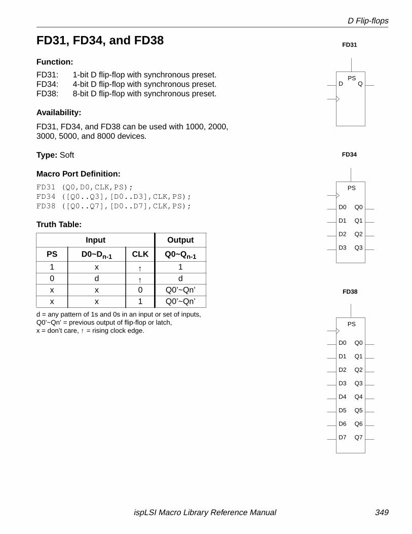
D Flip-flops
FD31, FD34, and FD38
Function:
FD31: 1-bit D flip-flop with synchronous preset.FD34: 4-bit D flip-flop with synchronous preset.FD38: 8-bit D flip-flop with synchronous preset.
Availability:
FD31, FD34, and FD38 can be used with 1000, 2000,3000, 5000, and 8000 devices.
Type: Soft
Macro Port Definition:
FD31 (Q0,D0,CLK,PS);FD34 ([Q0..Q3],[D0..D3],CLK,PS);FD38 ([Q0..Q7],[D0..D7],CLK,PS);
Truth Table:
d = any pattern of 1s and 0s in an input or set of inputs,Q0’~Qn’ = previous output of flip-flop or latch,x = don’t care, ↑ = rising clock edge.
Input Output
PS D0~Dn-1 CLK Q0~Qn-1
1 x ↑ 10 d ↑ dx x 0 Q0’~Qn’x x 1 Q0’~Qn’
FD31
FD38
D Q
FD34
Q3
Q2
Q1
Q0D0
D1
D2
D3
D7
D6
D5
D4 Q4
Q5
Q6
Q7
PS
PS
PS
Q3
Q2
Q1
Q0D0
D1
D2
D3
ispLSI Macro Library Reference Manual 349
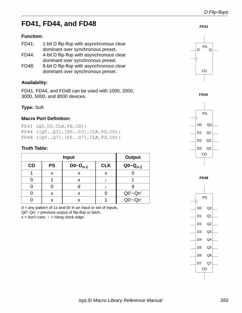
D Flip-flops
FD41, FD44, and FD48
Function:
FD41: 1-bit D flip-flop with asynchronous cleardominant over synchronous preset.
FD44: 4-bit D flip-flop with asynchronous cleardominant over synchronous preset.
FD48: 8-bit D flip-flop with asynchronous cleardominant over synchronous preset.
Availability:
FD41, FD44, and FD48 can be used with 1000, 2000,3000, 5000, and 8000 devices.
Type: Soft
Macro Port Definition:
FD41 (Q0,D0,CLK,PS,CD);FD44 ([Q0..Q3],[D0..D3],CLK,PS,CD);FD48 ([Q0..Q7],[D0..D7],CLK,PS,CD);
Truth Table:
d = any pattern of 1s and 0s in an input or set of inputs,Q0’~Qn’ = previous output of flip-flop or latch,x = don’t care, ↑ = rising clock edge.
Input Output
CD PS D0~Dn-1 CLK Q0~Qn-1
1 x x x 00 1 x ↑ 10 0 d ↑ d0 x x 0 Q0’~Qn’0 x x 1 Q0’~Qn’
FD41
FD48
D Q
FD44
Q3
Q2
Q1
Q0D0
D1
D2
D3
D7
D6
D5
D4 Q4
Q5
Q6
Q7
PS
PS
PS
Q3
Q2
Q1
Q0D0
D1
D2
D3
CD
CD
CD
ispLSI Macro Library Reference Manual 350
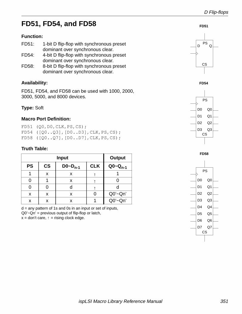
D Flip-flops
FD51, FD54, and FD58
Function:
FD51: 1-bit D flip-flop with synchronous presetdominant over synchronous clear.
FD54: 4-bit D flip-flop with synchronous presetdominant over synchronous clear.
FD58: 8-bit D flip-flop with synchronous presetdominant over synchronous clear.
Availability:
FD51, FD54, and FD58 can be used with 1000, 2000,3000, 5000, and 8000 devices.
Type: Soft
Macro Port Definition:
FD51 (Q0,D0,CLK,PS,CS);FD54 ([Q0..Q3],[D0..D3],CLK,PS,CS);FD58 ([Q0..Q7],[D0..D7],CLK,PS,CS);
Truth Table:
d = any pattern of 1s and 0s in an input or set of inputs,Q0’~Qn’ = previous output of flip-flop or latch,x = don’t care, ↑ = rising clock edge.
Input Output
PS CS D0~Dn-1 CLK Q0~Qn-1
1 x x ↑ 10 1 x ↑ 00 0 d ↑ dx x x 0 Q0’~Qn’x x x 1 Q0’~Qn’
FD51
FD58
D Q
FD54
Q3
Q2
Q1
Q0D0
D1
D2
D3
D7
D6
D5
D4 Q4
Q5
Q6
Q7
PS
PS
PS
Q3
Q2
Q1
Q0D0
D1
D2
D3
CS
CS
CS
ispLSI Macro Library Reference Manual 351
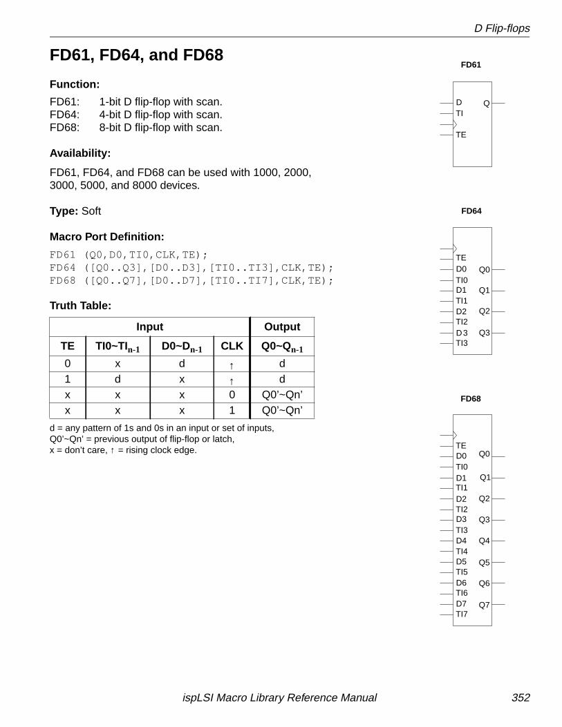
D Flip-flops
FD61, FD64, and FD68
Function:
FD61: 1-bit D flip-flop with scan.FD64: 4-bit D flip-flop with scan.FD68: 8-bit D flip-flop with scan.
Availability:
FD61, FD64, and FD68 can be used with 1000, 2000,3000, 5000, and 8000 devices.
Type: Soft
Macro Port Definition:
FD61 (Q0,D0,TI0,CLK,TE);FD64 ([Q0..Q3],[D0..D3],[TI0..TI3],CLK,TE);FD68 ([Q0..Q7],[D0..D7],[TI0..TI7],CLK,TE);
Truth Table:
d = any pattern of 1s and 0s in an input or set of inputs,Q0’~Qn’ = previous output of flip-flop or latch,x = don’t care, ↑ = rising clock edge.
Input Output
TE TI0~TIn-1 D0~Dn-1 CLK Q0~Qn-1
0 x d ↑ d1 d x ↑ dx x x 0 Q0’~Qn’x x x 1 Q0’~Qn’
TI0
Q4
Q5
Q6
Q7
D4
D5
D6
D7
D3
D2
D1
D0
Q3
Q2
Q1
Q0
TI1
TI2
TI3
TI4
TI5
TI6
TI7
TE
TE
TI3
TI2
TI1
TI0
D3
D2
D1
D0
Q3
Q2
Q1
Q0
TIQD
TE
FD61
FD68
FD64
ispLSI Macro Library Reference Manual 352
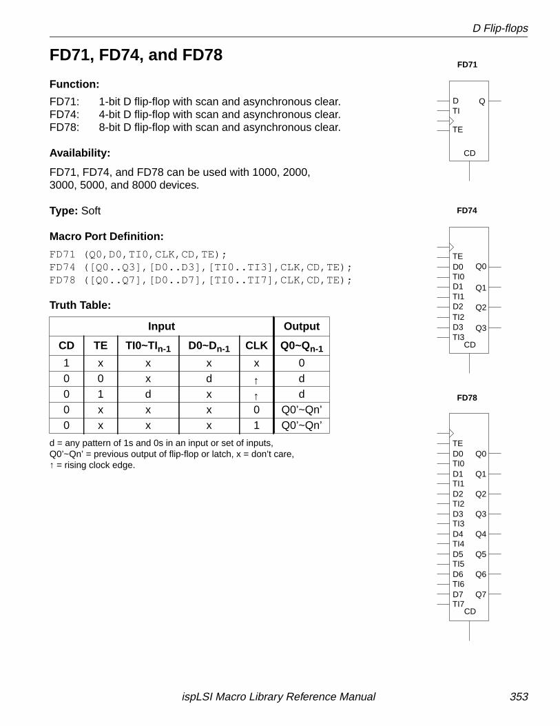
D Flip-flops
FD71, FD74, and FD78
Function:
FD71: 1-bit D flip-flop with scan and asynchronous clear.FD74: 4-bit D flip-flop with scan and asynchronous clear.FD78: 8-bit D flip-flop with scan and asynchronous clear.
Availability:
FD71, FD74, and FD78 can be used with 1000, 2000,3000, 5000, and 8000 devices.
Type: Soft
Macro Port Definition:
FD71 (Q0,D0,TI0,CLK,CD,TE);FD74 ([Q0..Q3],[D0..D3],[TI0..TI3],CLK,CD,TE);FD78 ([Q0..Q7],[D0..D7],[TI0..TI7],CLK,CD,TE);
Truth Table:
d = any pattern of 1s and 0s in an input or set of inputs,Q0’~Qn’ = previous output of flip-flop or latch, x = don’t care,↑ = rising clock edge.
Input Output
CD TE TI0~TIn-1 D0~Dn-1 CLK Q0~Qn-1
1 x x x x 00 0 x d ↑ d0 1 d x ↑ d0 x x x 0 Q0’~Qn’0 x x x 1 Q0’~Qn’
TI0
Q4
Q5
Q6
Q7
D4
D5
D6
D7
D3
D2
D1
D0
Q3
Q2
Q1
Q0
TI1
TI2
TI3
TI4
TI5
TI6
TI7
TE
TE
TI3
TI2
TI1
TI0
D3
D2
D1
D0
Q3
Q2
Q1
Q0
TIQD
TE
FD71
FD78
FD74
CD
CD
CD
ispLSI Macro Library Reference Manual 353
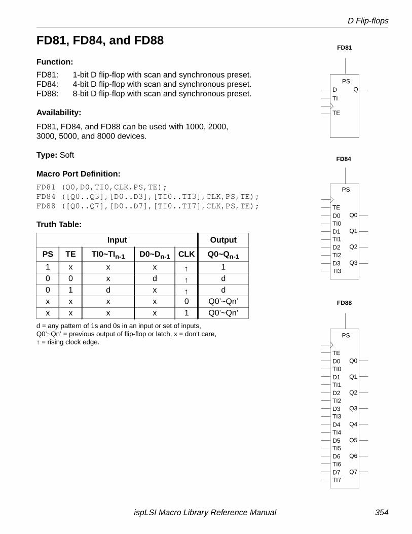
D Flip-flops
FD81, FD84, and FD88
Function:
FD81: 1-bit D flip-flop with scan and synchronous preset.FD84: 4-bit D flip-flop with scan and synchronous preset.FD88: 8-bit D flip-flop with scan and synchronous preset.
Availability:
FD81, FD84, and FD88 can be used with 1000, 2000,3000, 5000, and 8000 devices.
Type: Soft
Macro Port Definition:
FD81 (Q0,D0,TI0,CLK,PS,TE);FD84 ([Q0..Q3],[D0..D3],[TI0..TI3],CLK,PS,TE);FD88 ([Q0..Q7],[D0..D7],[TI0..TI7],CLK,PS,TE);
Truth Table:
d = any pattern of 1s and 0s in an input or set of inputs,Q0’~Qn’ = previous output of flip-flop or latch, x = don’t care,↑ = rising clock edge.
Input Output
PS TE TI0~TIn-1 D0~Dn-1 CLK Q0~Qn-1
1 x x x ↑ 10 0 x d ↑ d0 1 d x ↑ dx x x x 0 Q0’~Qn’x x x x 1 Q0’~Qn’
TI0
Q4
Q5
Q6
Q7
D4
D5
D6
D7
D3
D2
D1
D0
Q3
Q2
Q1
Q0
TI1
TI2
TI3
TI4
TI5
TI6
TI7
TE
TE
TI3
TI2
TI1
TI0
D3
D2
D1
D0
Q3
Q2
Q1
Q0
TI
QD
TE
FD81
FD88
FD84
PS
PS
PS
ispLSI Macro Library Reference Manual 354
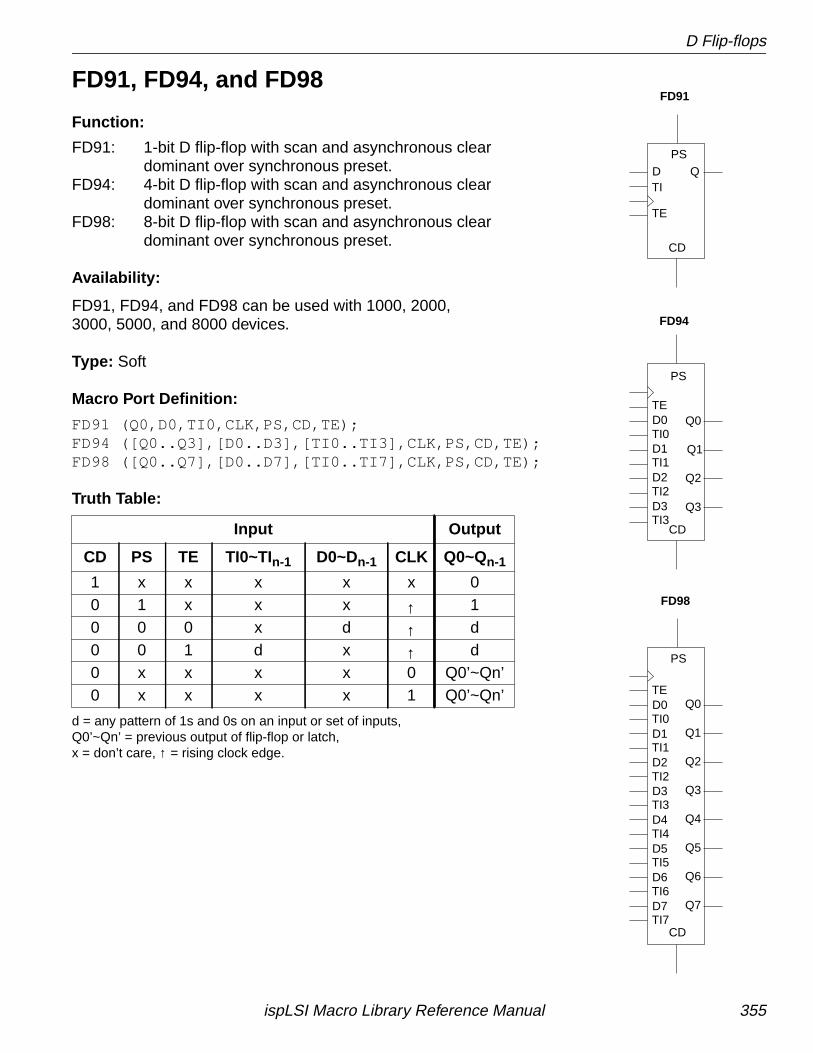
D Flip-flops
FD91, FD94, and FD98
Function:
FD91: 1-bit D flip-flop with scan and asynchronous cleardominant over synchronous preset.
FD94: 4-bit D flip-flop with scan and asynchronous cleardominant over synchronous preset.
FD98: 8-bit D flip-flop with scan and asynchronous cleardominant over synchronous preset.
Availability:
FD91, FD94, and FD98 can be used with 1000, 2000,3000, 5000, and 8000 devices.
Type: Soft
Macro Port Definition:
FD91 (Q0,D0,TI0,CLK,PS,CD,TE);FD94 ([Q0..Q3],[D0..D3],[TI0..TI3],CLK,PS,CD,TE);FD98 ([Q0..Q7],[D0..D7],[TI0..TI7],CLK,PS,CD,TE);
Truth Table:
d = any pattern of 1s and 0s on an input or set of inputs,Q0’~Qn’ = previous output of flip-flop or latch,x = don’t care, ↑ = rising clock edge.
Input Output
CD PS TE TI0~TIn-1 D0~Dn-1 CLK Q0~Qn-1
1 x x x x x 00 1 x x x ↑ 10 0 0 x d ↑ d0 0 1 d x ↑ d0 x x x x 0 Q0’~Qn’0 x x x x 1 Q0’~Qn’
TI0
Q4
Q5
Q6
Q7
D4
D5
D6
D7
D3
D2
D1
D0
Q3
Q2
Q1
Q0
TI1
TI2
TI3
TI4
TI5
TI6
TI7
TE
TE
TI3
TI2
TI1
TI0
D3
D2
D1
D0
Q3
Q2
Q1
Q0
TIQD
TE
FD91
FD98
FD94
PS
PS
PS
CD
CD
CD
ispLSI Macro Library Reference Manual 355
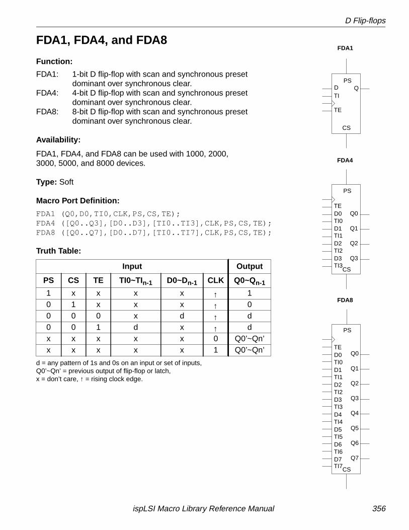
D Flip-flops
FDA1, FDA4, and FDA8
Function:
FDA1: 1-bit D flip-flop with scan and synchronous presetdominant over synchronous clear.
FDA4: 4-bit D flip-flop with scan and synchronous presetdominant over synchronous clear.
FDA8: 8-bit D flip-flop with scan and synchronous presetdominant over synchronous clear.
Availability:
FDA1, FDA4, and FDA8 can be used with 1000, 2000,3000, 5000, and 8000 devices.
Type: Soft
Macro Port Definition:
FDA1 (Q0,D0,TI0,CLK,PS,CS,TE);FDA4 ([Q0..Q3],[D0..D3],[TI0..TI3],CLK,PS,CS,TE);FDA8 ([Q0..Q7],[D0..D7],[TI0..TI7],CLK,PS,CS,TE);
Truth Table:
d = any pattern of 1s and 0s on an input or set of inputs,Q0’~Qn’ = previous output of flip-flop or latch,x = don’t care, ↑ = rising clock edge.
Input Output
PS CS TE TI0~TIn-1 D0~Dn-1 CLK Q0~Qn-1
1 x x x x ↑ 10 1 x x x ↑ 00 0 0 x d ↑ d0 0 1 d x ↑ dx x x x x 0 Q0’~Qn’x x x x x 1 Q0’~Qn’
TI0
Q4
Q5
Q6
Q7
D4
D5
D6
D7
D3
D2
D1
D0
Q3
Q2
Q1
Q0
TI1
TI2
TI3
TI4
TI5
TI6
TI7
TE
TE
TI3
TI2
TI1
TI0
D3
D2
D1
D0
Q3
Q2
Q1
Q0
TIQD
TE
FDA1
FDA8
FDA4
PS
PS
PS
CS
CS
CS
ispLSI Macro Library Reference Manual 356
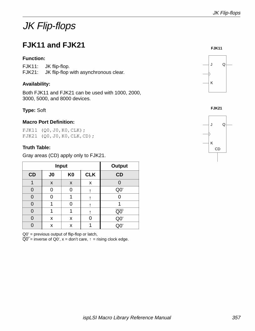
JK Flip-flops
JK Flip-flops
FJK11 and FJK21
Function:
FJK11: JK flip-flop.FJK21: JK flip-flop with asynchronous clear.
Availability:
Both FJK11 and FJK21 can be used with 1000, 2000,3000, 5000, and 8000 devices.
Type: Soft
Macro Port Definition:
FJK11 (Q0,J0,K0,CLK);FJK21 (Q0,J0,K0,CLK,CD);
Truth Table:
Gray areas (CD) apply only to FJK21.
Q0’ = previous output of flip-flop or latch,Q0’ = inverse of Q0’, x = don’t care, ↑ = rising clock edge.
Input Output
CD J0 K0 CLK CD
1 x x x 00 0 0 ↑ Q0’0 0 1 ↑ 00 1 0 ↑ 10 1 1 ↑ Q0’0 x x 0 Q0’0 x x 1 Q0’
FJK11
FJK21
J
K
Q
QJ
K
CD
ispLSI Macro Library Reference Manual 357
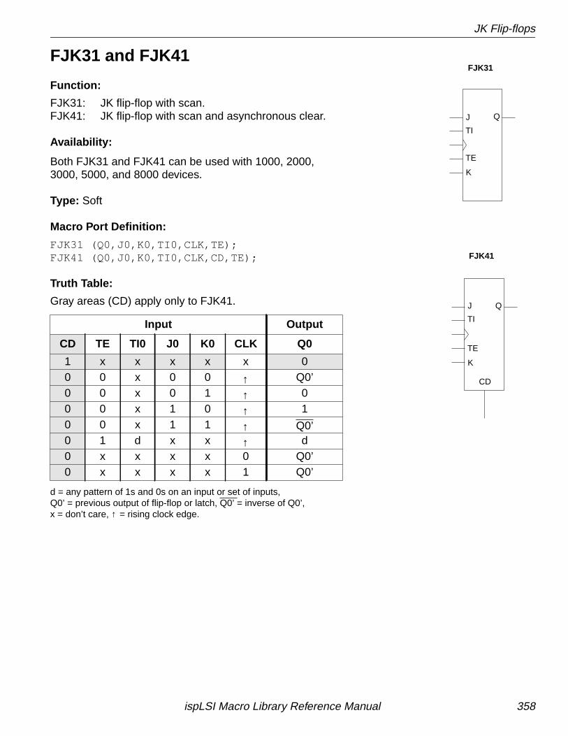
JK Flip-flops
FJK31 and FJK41
Function:
FJK31: JK flip-flop with scan.FJK41: JK flip-flop with scan and asynchronous clear.
Availability:
Both FJK31 and FJK41 can be used with 1000, 2000,3000, 5000, and 8000 devices.
Type: Soft
Macro Port Definition:
FJK31 (Q0,J0,K0,TI0,CLK,TE);FJK41 (Q0,J0,K0,TI0,CLK,CD,TE);
Truth Table:
Gray areas (CD) apply only to FJK41.
d = any pattern of 1s and 0s on an input or set of inputs,Q0’ = previous output of flip-flop or latch, Q0’ = inverse of Q0’,x = don’t care, ↑ = rising clock edge.
Input Output
CD TE TI0 J0 K0 CLK Q0
1 x x x x x 00 0 x 0 0 ↑ Q0’0 0 x 0 1 ↑ 00 0 x 1 0 ↑ 10 0 x 1 1 ↑ Q0’0 1 d x x ↑ d0 x x x x 0 Q0’0 x x x x 1 Q0’
J Q
K
TI
TE
J Q
K
TI
TE
FJK31
FJK41
CD
ispLSI Macro Library Reference Manual 358
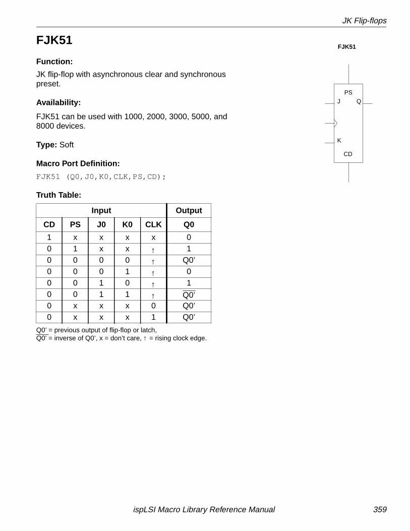
JK Flip-flops
FJK51
Function:
JK flip-flop with asynchronous clear and synchronouspreset.
Availability:
FJK51 can be used with 1000, 2000, 3000, 5000, and8000 devices.
Type: Soft
Macro Port Definition:
FJK51 (Q0,J0,K0,CLK,PS,CD);
Truth Table:
Q0’ = previous output of flip-flop or latch,Q0’ = inverse of Q0’, x = don’t care, ↑ = rising clock edge.
Input Output
CD PS J0 K0 CLK Q0
1 x x x x 00 1 x x ↑ 10 0 0 0 ↑ Q0’0 0 0 1 ↑ 00 0 1 0 ↑ 10 0 1 1 ↑ Q0’0 x x x 0 Q0’0 x x x 1 Q0’
FJK51
CD
PS
K
QJ
ispLSI Macro Library Reference Manual 359
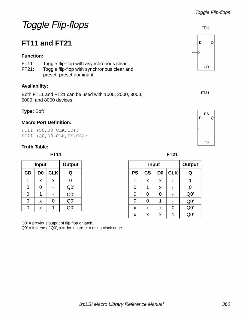
Toggle Flip-flops
Toggle Flip-flops
FT11 and FT21
Function:
FT11: Toggle flip-flop with asynchronous clear.FT21: Toggle flip-flop with synchronous clear and
preset, preset dominant.
Availability:
Both FT11 and FT21 can be used with 1000, 2000, 3000,5000, and 8000 devices.
Type: Soft
Macro Port Definition:
FT11 (Q0,D0,CLK,CD);FT21 (Q0,D0,CLK,PS,CS);
Truth Table:
FT11 FT21
Q0’ = previous output of flip-flop or latch,Q0’ = inverse of Q0’, x = don’t care, ↑ = rising clock edge.
Input Output Input Output
CD D0 CLK Q PS CS D0 CLK Q
1 x x 0 1 x x ↑ 10 0 ↑ Q0’ 0 1 x ↑ 00 1 ↑ Q0’ 0 0 0 ↑ Q0’0 x 0 Q0’ 0 0 1 ↑ Q0’0 x 1 Q0’ x x x 0 Q0’
x x x 1 Q0’
FT11
FT21
QD
CD
Q
CS
PSD
ispLSI Macro Library Reference Manual 360
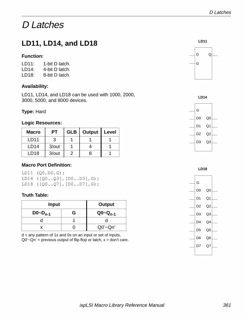
D Latches
D Latches
LD11, LD14, and LD18
Function:
LD11: 1-bit D latch.LD14: 4-bit D latch.LD18: 8-bit D latch.
Availability:
LD11, LD14, and LD18 can be used with 1000, 2000,3000, 5000, and 8000 devices.
Type: Hard
Logic Resources:
Macro Port Definition:
LD11 (Q0,D0,G);LD14 ([Q0..Q3],[D0..D3],G);LD18 ([Q0..Q7],[D0..D7],G);
Truth Table:
d = any pattern of 1s and 0s on an input or set of inputs,Q0’~Qn’ = previous output of flip-flop or latch, x = don’t care.
Macro PT GLB Output Level
LD11 3 1 1 1LD14 3/out 1 4 1LD18 3/out 2 8 1
Input Output
D0~Dn-1 G Q0~Qn-1
d 1 dx 0 Q0’~Qn’
LD11
LD18
D Q
LD14
Q3
Q2
Q1
Q0D0
D1
D2
D3
Q3
Q2
Q1
Q0D0
D1
D2
D3
D7
D6
D5
D4 Q4
Q5
Q6
Q7
G
G
G
ispLSI Macro Library Reference Manual 361
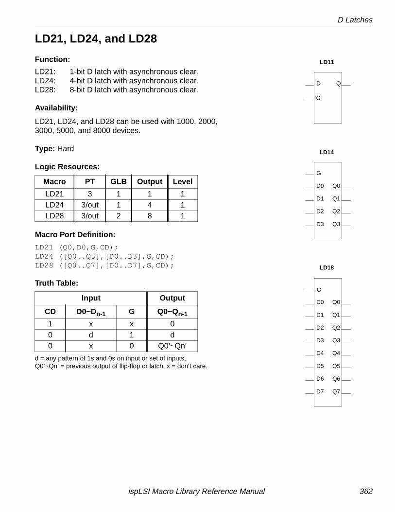
D Latches
LD21, LD24, and LD28
Function:
LD21: 1-bit D latch with asynchronous clear.LD24: 4-bit D latch with asynchronous clear.LD28: 8-bit D latch with asynchronous clear.
Availability:
LD21, LD24, and LD28 can be used with 1000, 2000,3000, 5000, and 8000 devices.
Type: Hard
Logic Resources:
Macro Port Definition:
LD21 (Q0,D0,G,CD);LD24 ([Q0..Q3],[D0..D3],G,CD);LD28 ([Q0..Q7],[D0..D7],G,CD);
Truth Table:
d = any pattern of 1s and 0s on input or set of inputs,Q0’~Qn’ = previous output of flip-flop or latch, x = don’t care.
Macro PT GLB Output Level
LD21 3 1 1 1LD24 3/out 1 4 1LD28 3/out 2 8 1
Input Output
CD D0~Dn-1 G Q0~Qn-1
1 x x 00 d 1 d0 x 0 Q0’~Qn’
LD11
LD18
D Q
LD14
Q3
Q2
Q1
Q0D0
D1
D2
D3
Q3
Q2
Q1
Q0D0
D1
D2
D3
D7
D6
D5
D4 Q4
Q5
Q6
Q7
G
G
G
ispLSI Macro Library Reference Manual 362
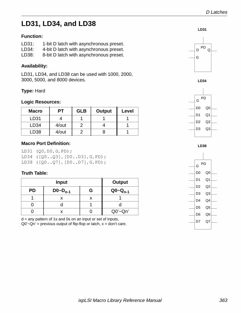
D Latches
LD31, LD34, and LD38
Function:
LD31: 1-bit D latch with asynchronous preset.LD34: 4-bit D latch with asynchronous preset.LD38: 8-bit D latch with asynchronous preset.
Availability:
LD31, LD34, and LD38 can be used with 1000, 2000,3000, 5000, and 8000 devices.
Type: Hard
Logic Resources:
Macro Port Definition:
LD31 (Q0,D0,G,PD);LD34 ([Q0..Q3],[D0..D3],G,PD);LD38 ([Q0..Q7],[D0..D7],G,PD);
Truth Table:
d = any pattern of 1s and 0s on an input or set of inputs,Q0’~Qn’ = previous output of flip-flop or latch, x = don’t care.
Macro PT GLB Output Level
LD31 4 1 1 1LD34 4/out 2 4 1LD38 4/out 2 8 1
Input Output
PD D0~Dn-1 G Q0~Qn-1
1 x x 10 d 1 d0 x 0 Q0’~Qn’
LD31
LD38
D Q
LD34
Q3
Q2
Q1
Q0D0
D1
D2
D3
D7
D6
D5
D4 Q4
Q5
Q6
Q7
PD
PD
PD
Q3
Q2
Q1
Q0D0
D1
D2
D3
G
G
G
ispLSI Macro Library Reference Manual 363
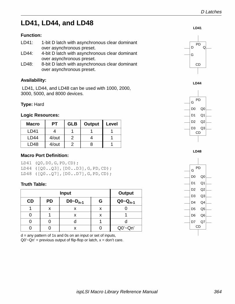
D Latches
LD41, LD44, and LD48
Function:
LD41: 1-bit D latch with asynchronous clear dominantover asynchronous preset.
LD44: 4-bit D latch with asynchronous clear dominantover asynchronous preset.
LD48: 8-bit D latch with asynchronous clear dominantover asynchronous preset.
Availability:
LD41, LD44, and LD48 can be used with 1000, 2000,3000, 5000, and 8000 devices.
Type: Hard
Logic Resources:
Macro Port Definition:
LD41 (Q0,D0,G,PD,CD);LD44 ([Q0..Q3],[D0..D3],G,PD,CD);LD48 ([Q0..Q7],[D0..D7],G,PD,CD);
Truth Table:
d = any pattern of 1s and 0s on an input or set of inputs,Q0’~Qn’ = previous output of flip-flop or latch, x = don’t care.
Macro PT GLB Output Level
LD41 4 1 1 1LD44 4/out 2 4 1LD48 4/out 2 8 1
Input Output
CD PD D0~Dn-1 G Q0~Qn-1
1 x x x 00 1 x x 10 0 d 1 d0 0 x 0 Q0’~Qn’
LD41
LD48
D Q
LD44
Q3
Q2
Q1
Q0D0
D1
D2
D3
D7
D6
D5
D4 Q4
Q5
Q6
Q7
PD
PD
PD
Q3
Q2
Q1
Q0D0
D1
D2
D3
CD
CD
CD
G
G
G
ispLSI Macro Library Reference Manual 364
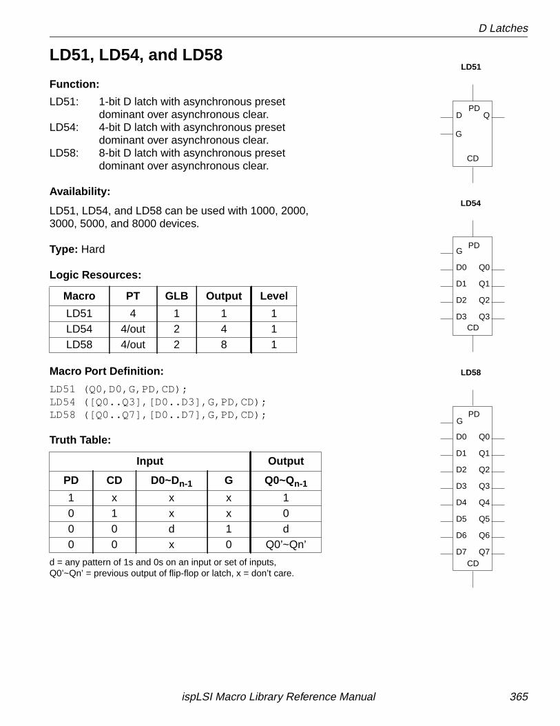
D Latches
LD51, LD54, and LD58
Function:
LD51: 1-bit D latch with asynchronous presetdominant over asynchronous clear.
LD54: 4-bit D latch with asynchronous presetdominant over asynchronous clear.
LD58: 8-bit D latch with asynchronous presetdominant over asynchronous clear.
Availability:
LD51, LD54, and LD58 can be used with 1000, 2000,3000, 5000, and 8000 devices.
Type: Hard
Logic Resources:
Macro Port Definition:
LD51 (Q0,D0,G,PD,CD);LD54 ([Q0..Q3],[D0..D3],G,PD,CD);LD58 ([Q0..Q7],[D0..D7],G,PD,CD);
Truth Table:
d = any pattern of 1s and 0s on an input or set of inputs,Q0’~Qn’ = previous output of flip-flop or latch, x = don’t care.
Macro PT GLB Output Level
LD51 4 1 1 1LD54 4/out 2 4 1LD58 4/out 2 8 1
Input Output
PD CD D0~Dn-1 G Q0~Qn-1
1 x x x 10 1 x x 00 0 d 1 d0 0 x 0 Q0’~Qn’
LD51
LD58
D Q
LD54
Q3
Q2
Q1
Q0D0
D1
D2
D3
D7
D6
D5
D4 Q4
Q5
Q6
Q7
PD
PD
PD
Q3
Q2
Q1
Q0D0
D1
D2
D3
CD
CD
CD
G
G
G
ispLSI Macro Library Reference Manual 365
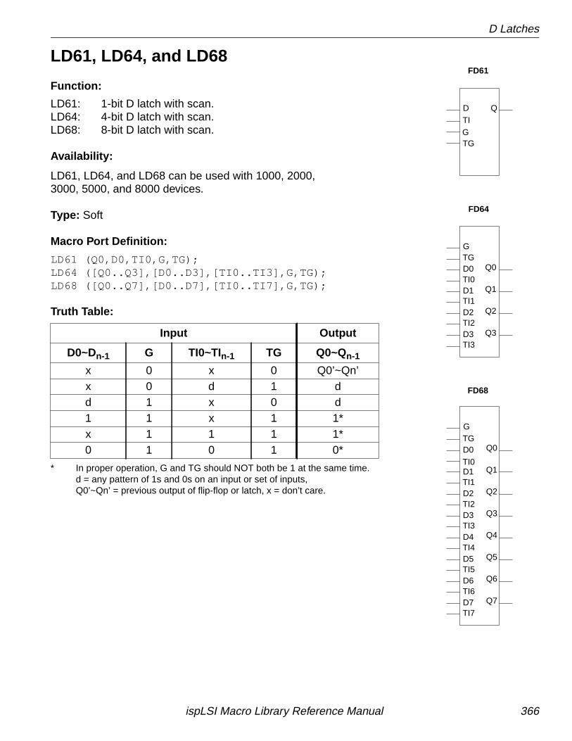
D Latches
LD61, LD64, and LD68
Function:
LD61: 1-bit D latch with scan.LD64: 4-bit D latch with scan.LD68: 8-bit D latch with scan.
Availability:
LD61, LD64, and LD68 can be used with 1000, 2000,3000, 5000, and 8000 devices.
Type: Soft
Macro Port Definition:
LD61 (Q0,D0,TI0,G,TG);LD64 ([Q0..Q3],[D0..D3],[TI0..TI3],G,TG);LD68 ([Q0..Q7],[D0..D7],[TI0..TI7],G,TG);
Truth Table:
* In proper operation, G and TG should NOT both be 1 at the same time.d = any pattern of 1s and 0s on an input or set of inputs,Q0’~Qn’ = previous output of flip-flop or latch, x = don’t care.
Input Output
D0~Dn-1 G TI0~TIn-1 TG Q0~Qn-1
x 0 x 0 Q0’~Qn’x 0 d 1 dd 1 x 0 d1 1 x 1 1*x 1 1 1 1*0 1 0 1 0*
TI0
Q4
Q5
Q6
Q7
D4
D5
D6
D7
D3
D2
D1
D0
Q3
Q2
Q1
Q0
TI1
TI2
TI3
TI4
TI5
TI6
TI7
TG
TG
TI3
TI2
TI1
TI0
D3
D2
D1
D0
Q3
Q2
Q1
Q0
TIQD
TG
FD61
FD68
FD64
G
G
G
ispLSI Macro Library Reference Manual 366
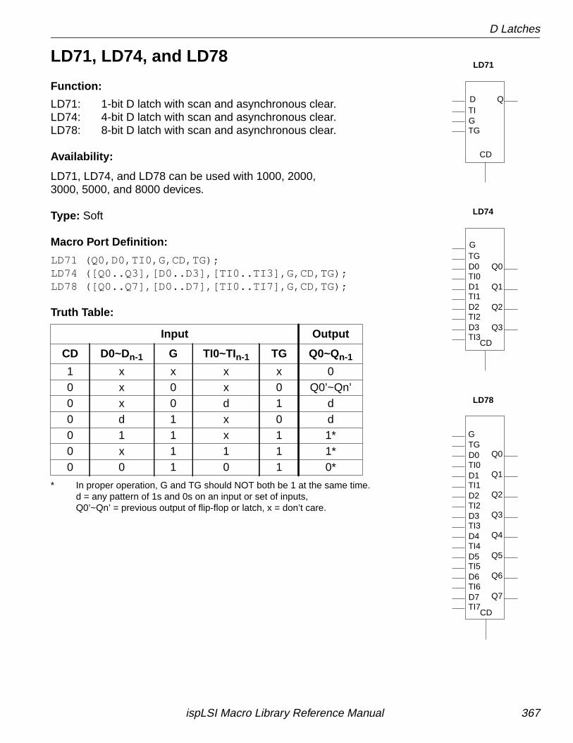
D Latches
LD71, LD74, and LD78
Function:
LD71: 1-bit D latch with scan and asynchronous clear.LD74: 4-bit D latch with scan and asynchronous clear.LD78: 8-bit D latch with scan and asynchronous clear.
Availability:
LD71, LD74, and LD78 can be used with 1000, 2000,3000, 5000, and 8000 devices.
Type: Soft
Macro Port Definition:
LD71 (Q0,D0,TI0,G,CD,TG);LD74 ([Q0..Q3],[D0..D3],[TI0..TI3],G,CD,TG);LD78 ([Q0..Q7],[D0..D7],[TI0..TI7],G,CD,TG);
Truth Table:
* In proper operation, G and TG should NOT both be 1 at the same time.d = any pattern of 1s and 0s on an input or set of inputs,Q0’~Qn’ = previous output of flip-flop or latch, x = don’t care.
Input Output
CD D0~Dn-1 G TI0~TIn-1 TG Q0~Qn-1
1 x x x x 00 x 0 x 0 Q0’~Qn’0 x 0 d 1 d0 d 1 x 0 d0 1 1 x 1 1*0 x 1 1 1 1*0 0 1 0 1 0* TI0
Q4
Q5
Q6
Q7
D4
D5
D6
D7
D3
D2
D1
D0
Q3
Q2
Q1
Q0
TI1
TI2
TI3
TI4
TI5
TI6
TI7
TG
TG
TI3
TI2
TI1
TI0
D3
D2
D1
D0
Q3
Q2
Q1
Q0
TIQD
TG
LD71
LD78
LD74
CD
CD
CD
G
G
G
ispLSI Macro Library Reference Manual 367
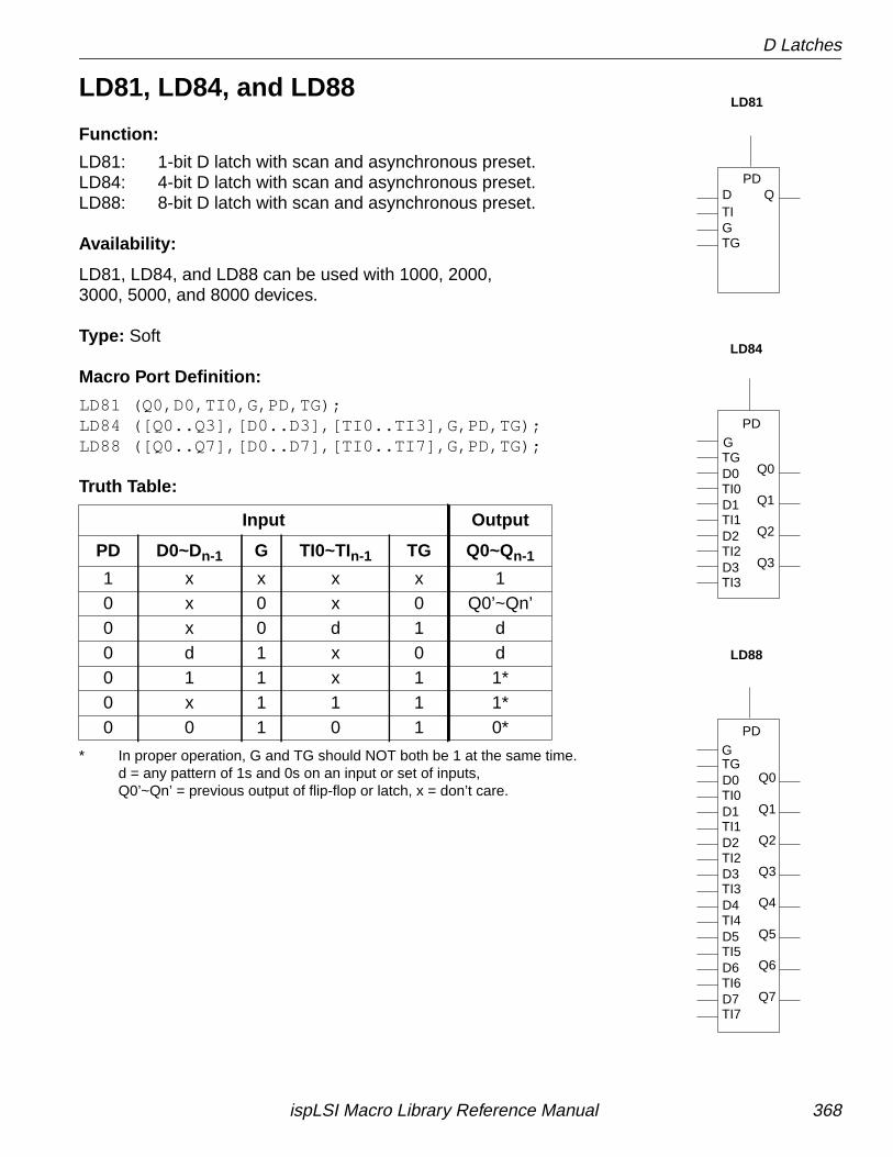
D Latches
LD81, LD84, and LD88
Function:
LD81: 1-bit D latch with scan and asynchronous preset.LD84: 4-bit D latch with scan and asynchronous preset.LD88: 8-bit D latch with scan and asynchronous preset.
Availability:
LD81, LD84, and LD88 can be used with 1000, 2000,3000, 5000, and 8000 devices.
Type: Soft
Macro Port Definition:
LD81 (Q0,D0,TI0,G,PD,TG);LD84 ([Q0..Q3],[D0..D3],[TI0..TI3],G,PD,TG);LD88 ([Q0..Q7],[D0..D7],[TI0..TI7],G,PD,TG);
Truth Table:
* In proper operation, G and TG should NOT both be 1 at the same time.d = any pattern of 1s and 0s on an input or set of inputs,Q0’~Qn’ = previous output of flip-flop or latch, x = don’t care.
Input Output
PD D0~Dn-1 G TI0~TIn-1 TG Q0~Qn-1
1 x x x x 10 x 0 x 0 Q0’~Qn’0 x 0 d 1 d0 d 1 x 0 d0 1 1 x 1 1*0 x 1 1 1 1*0 0 1 0 1 0*
TG
TI
TI0
Q4
Q5
Q6
Q7
D4
D5
D6
D7
D3
D2
D1
D0
Q3
Q2
Q1
Q0
TI1
TI2
TI3
TI4
TI5
TI6
TI7
TG
TG
TI3
TI2
TI1
TI0
D3
D2
D1
D0
Q3
Q2
Q1
Q0
QD
LD81
LD88
LD84
PD
PD
PD
G
G
G
ispLSI Macro Library Reference Manual 368
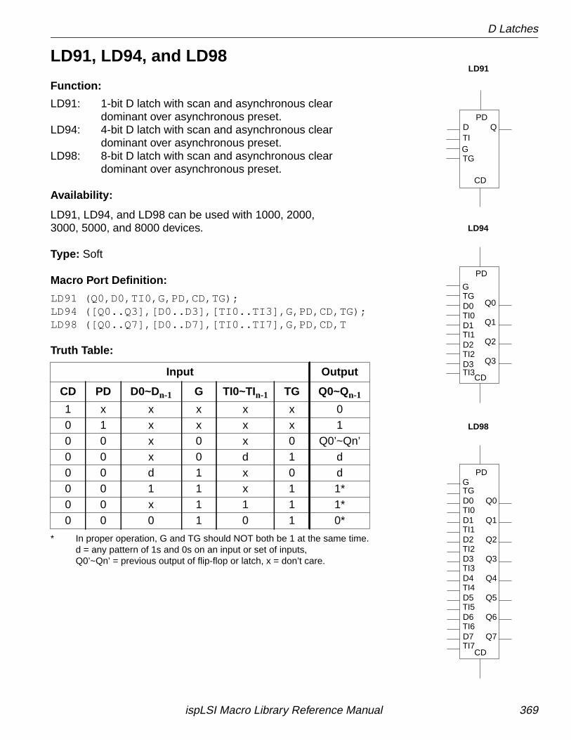
D Latches
LD91, LD94, and LD98
Function:
LD91: 1-bit D latch with scan and asynchronous cleardominant over asynchronous preset.
LD94: 4-bit D latch with scan and asynchronous cleardominant over asynchronous preset.
LD98: 8-bit D latch with scan and asynchronous cleardominant over asynchronous preset.
Availability:
LD91, LD94, and LD98 can be used with 1000, 2000,3000, 5000, and 8000 devices.
Type: Soft
Macro Port Definition:
LD91 (Q0,D0,TI0,G,PD,CD,TG);LD94 ([Q0..Q3],[D0..D3],[TI0..TI3],G,PD,CD,TG);LD98 ([Q0..Q7],[D0..D7],[TI0..TI7],G,PD,CD,T
Truth Table:
* In proper operation, G and TG should NOT both be 1 at the same time.d = any pattern of 1s and 0s on an input or set of inputs,Q0’~Qn’ = previous output of flip-flop or latch, x = don’t care.
Input Output
CD PD D0~Dn-1 G TI0~TIn-1 TG Q0~Qn-1
1 x x x x x 00 1 x x x x 10 0 x 0 x 0 Q0’~Qn’0 0 x 0 d 1 d0 0 d 1 x 0 d0 0 1 1 x 1 1*0 0 x 1 1 1 1*0 0 0 1 0 1 0*
TI0
Q4
Q5
Q6
Q7
D4
D5
D6
D7
D3
D2
D1
D0
Q3
Q2
Q1
Q0
TI1
TI2
TI3
TI4
TI5
TI6
TI7
TG
TG
TI3
TI2
TI1
TI0
D3
D2
D1
D0
Q3
Q2
Q1
Q0
TIQD
TG
LD91
LD98
LD94
PD
PD
PD
CD
CD
CD
G
G
G
ispLSI Macro Library Reference Manual 369
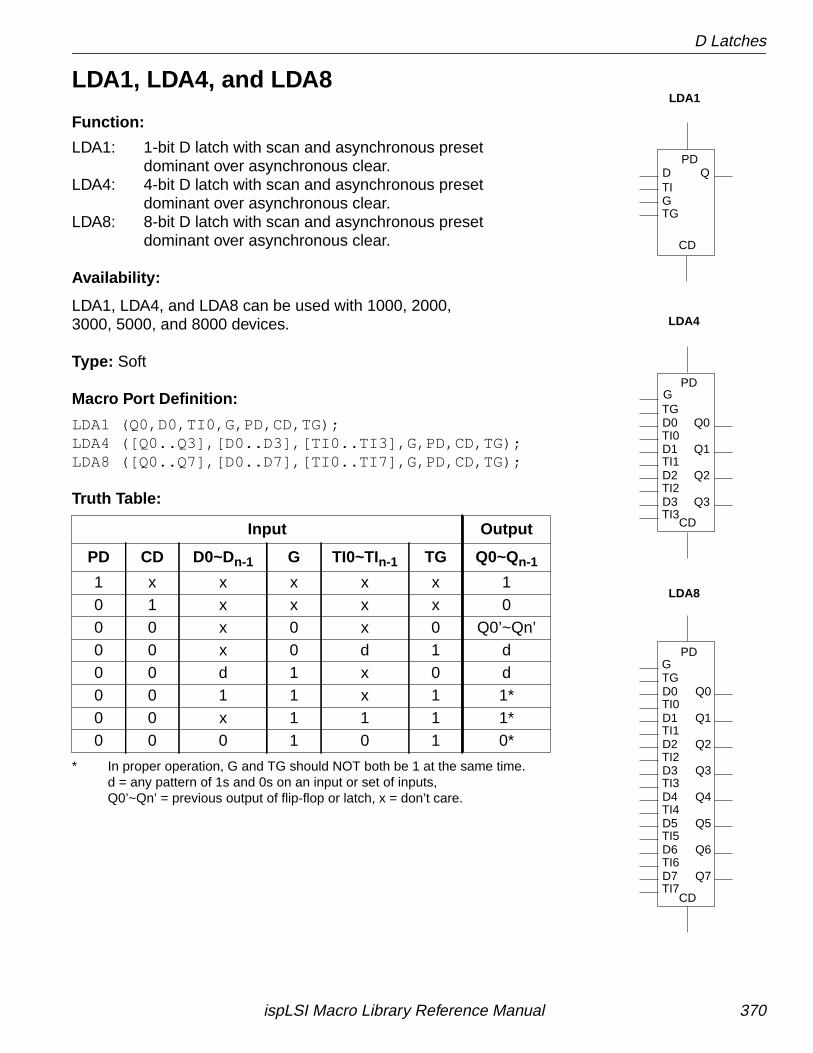
D Latches
LDA1, LDA4, and LDA8
Function:
LDA1: 1-bit D latch with scan and asynchronous presetdominant over asynchronous clear.
LDA4: 4-bit D latch with scan and asynchronous presetdominant over asynchronous clear.
LDA8: 8-bit D latch with scan and asynchronous presetdominant over asynchronous clear.
Availability:
LDA1, LDA4, and LDA8 can be used with 1000, 2000,3000, 5000, and 8000 devices.
Type: Soft
Macro Port Definition:
LDA1 (Q0,D0,TI0,G,PD,CD,TG);LDA4 ([Q0..Q3],[D0..D3],[TI0..TI3],G,PD,CD,TG);LDA8 ([Q0..Q7],[D0..D7],[TI0..TI7],G,PD,CD,TG);
Truth Table:
* In proper operation, G and TG should NOT both be 1 at the same time.d = any pattern of 1s and 0s on an input or set of inputs,Q0’~Qn’ = previous output of flip-flop or latch, x = don’t care.
Input Output
PD CD D0~Dn-1 G TI0~TIn-1 TG Q0~Qn-1
1 x x x x x 10 1 x x x x 00 0 x 0 x 0 Q0’~Qn’0 0 x 0 d 1 d0 0 d 1 x 0 d0 0 1 1 x 1 1*0 0 x 1 1 1 1*0 0 0 1 0 1 0*
TI0
Q4
Q5
Q6
Q7
D4
D5
D6
D7
D3
D2
D1
D0
Q3
Q2
Q1
Q0
TI1
TI2
TI3
TI4
TI5
TI6
TI7
TG
TG
TI3
TI2
TI1
TI0
D3
D2
D1
D0
Q3
Q2
Q1
Q0
TIQD
TG
LDA1
LDA8
LDA4
PD
PD
PD
CD
CD
CD
G
G
G
ispLSI Macro Library Reference Manual 370
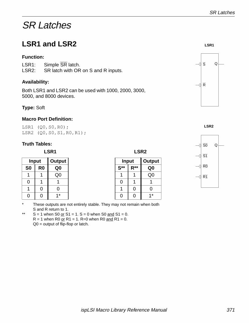
SR Latches
SR Latches
LSR1 and LSR2
Function:
LSR1: Simple SR latch.LSR2: SR latch with OR on S and R inputs.
Availability:
Both LSR1 and LSR2 can be used with 1000, 2000, 3000,5000, and 8000 devices.
Type: Soft
Macro Port Definition:
LSR1 (Q0,S0,R0);LSR2 (Q0,S0,S1,R0,R1);
Truth Tables:
LSR1 LSR2
* These outputs are not entirely stable. They may not remain when bothS and R return to 1.
** S = 1 when S0 or S1 = 1. S = 0 when S0 and S1 = 0.R = 1 when R0 or R1 = 1. R=0 when R0 and R1 = 0.Q0 = output of flip-flop or latch.
Input Output Input OutputS0 R0 Q0 S** R** Q01 1 Q0 1 1 Q00 1 1 0 1 11 0 0 1 0 00 0 1* 0 0 1*
R
S Q
LSR1
LSR2
S0
S1
R0
R1
Q
ispLSI Macro Library Reference Manual 371
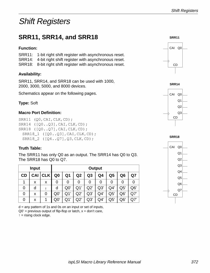
Shift Registers
Shift Registers
SRR11, SRR14, and SRR18
Function:
SRR11: 1-bit right shift register with asynchronous reset.SRR14: 4-bit right shift register with asynchronous reset.SRR18: 8-bit right shift register with asynchronous reset.
Availability:
SRR11, SRR14, and SRR18 can be used with 1000,2000, 3000, 5000, and 8000 devices.
Schematics appear on the following pages.
Type: Soft
Macro Port Definition:
SRR11 (Q0,CAI,CLK,CD);SRR14 ([Q0..Q3],CAI,CLK,CD);SRR18 ([Q0..Q7],CAI,CLK,CD);
SRR18_1 ([Q0..Q3],CAI,CLK,CD);SRR18_2 ([Q4..Q7],Q3,CLK,CD);
Truth Table:
The SRR11 has only Q0 as an output. The SRR14 has Q0 to Q3.The SRR18 has Q0 to Q7.
d = any pattern of 1s and 0s on an input or set of inputs,Q0’ = previous output of flip-flop or latch, x = don’t care,↑ = rising clock edge.
Input Output
CD CAI CLK Q0 Q1 Q2 Q3 Q4 Q5 Q6 Q7
1 x x 0 0 0 0 0 0 0 00 d ↑ d Q0’ Q1’ Q2’ Q3’ Q4’ Q5’ Q6’0 x 0 Q0’ Q1’ Q2’ Q3’ Q4’ Q5’ Q6’ Q7’0 x 1 Q0’ Q1’ Q2’ Q3’ Q4’ Q5’ Q6’ Q7’
CAI
CD
Q0
SRR11
SRR18
SRR14
Q3
Q2
Q1
Q0
CD
CAI
CAI
CD
Q0
Q1
Q2
Q3
Q4
Q5
Q6
Q7
ispLSI Macro Library Reference Manual 372
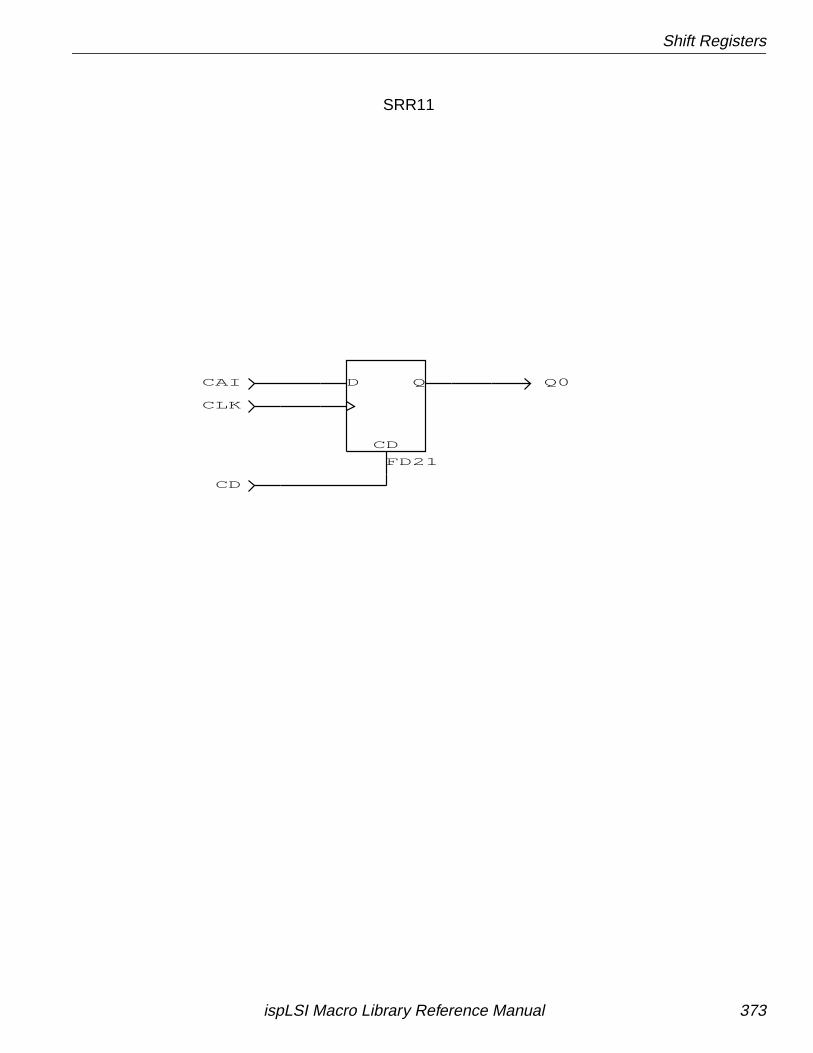
Shift Registers
CD
CLK
CAI Q0
CD
QD
FD21
SRR11
ispLSI Macro Library Reference Manual 373
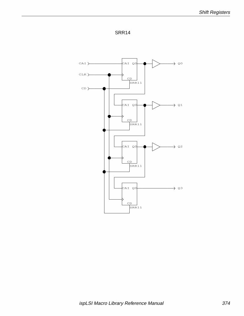
Shift Registers
SRR11
CAI
CD
Q0
SRR11
CAI
CD
Q0
SRR11
CAI
CD
Q0
SRR11
CAI
CD
Q0
CAI
CLK
CD
Q0
Q1
Q2
Q3
SRR14
ispLSI Macro Library Reference Manual 374
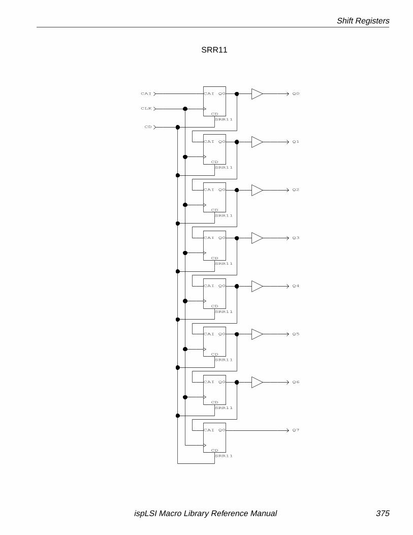
Shift Registers
SRR11
CAI
CD
Q0
SRR11
CAI
CD
Q0
SRR11
CAI
CD
Q0 Q3
Q2
Q1
Q0
CD
CLK
CAI
SRR11
CAI
CD
Q0
SRR11
CAI
CD
Q0
Q7
Q6
Q5
Q4
SRR11
CAI
CD
Q0
SRR11
CAI
CD
Q0
SRR11
CAI
CD
Q0
SRR11
ispLSI Macro Library Reference Manual 375
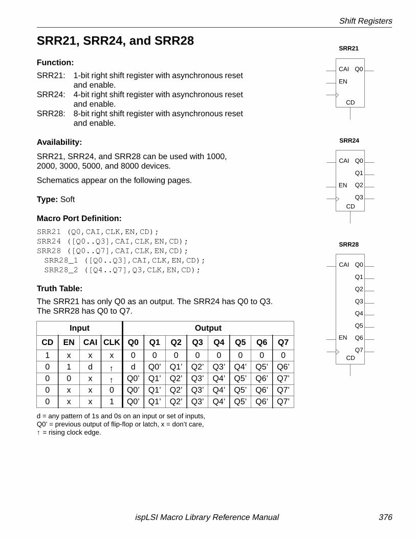
Shift Registers
SRR21, SRR24, and SRR28
Function:
SRR21: 1-bit right shift register with asynchronous resetand enable.
SRR24: 4-bit right shift register with asynchronous resetand enable.
SRR28: 8-bit right shift register with asynchronous resetand enable.
Availability:
SRR21, SRR24, and SRR28 can be used with 1000,2000, 3000, 5000, and 8000 devices.
Schematics appear on the following pages.
Type: Soft
Macro Port Definition:
SRR21 (Q0,CAI,CLK,EN,CD);SRR24 ([Q0..Q3],CAI,CLK,EN,CD);SRR28 ([Q0..Q7],CAI,CLK,EN,CD);
SRR28_1 ([Q0..Q3],CAI,CLK,EN,CD);SRR28_2 ([Q4..Q7],Q3,CLK,EN,CD);
Truth Table:
The SRR21 has only Q0 as an output. The SRR24 has Q0 to Q3.The SRR28 has Q0 to Q7.
d = any pattern of 1s and 0s on an input or set of inputs,Q0’ = previous output of flip-flop or latch, x = don’t care,↑ = rising clock edge.
Input Output
CD EN CAI CLK Q0 Q1 Q2 Q3 Q4 Q5 Q6 Q7
1 x x x 0 0 0 0 0 0 0 00 1 d ↑ d Q0’ Q1’ Q2’ Q3’ Q4’ Q5’ Q6’0 0 x ↑ Q0’ Q1’ Q2’ Q3’ Q4’ Q5’ Q6’ Q7’0 x x 0 Q0’ Q1’ Q2’ Q3’ Q4’ Q5’ Q6’ Q7’0 x x 1 Q0’ Q1’ Q2’ Q3’ Q4’ Q5’ Q6’ Q7’
CAI
CD
Q0
SRR21
SRR28
SRR24
Q3
Q2
Q1
Q0
CD
CAI
CAI
CD
Q0
Q1
Q2
Q3
Q4
Q5
Q6
Q7
EN
EN
EN
ispLSI Macro Library Reference Manual 376
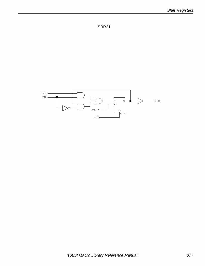
Shift Registers
Q0
CAI
CD
QD
FD21
EN
CLK
CD
SRR21
ispLSI Macro Library Reference Manual 377
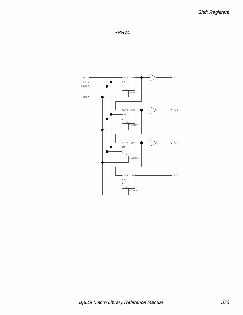
Shift Registers
EN
CAI
CD
EN
Q0
SRR21
CAI
CD
EN
Q0
SRR21
CAI
CD
EN
Q0
SRR21
CAI
CD
EN
Q0
SRR21
Q3
Q2
Q1
Q0
CD
CAI
CLK
SRR24
ispLSI Macro Library Reference Manual 378
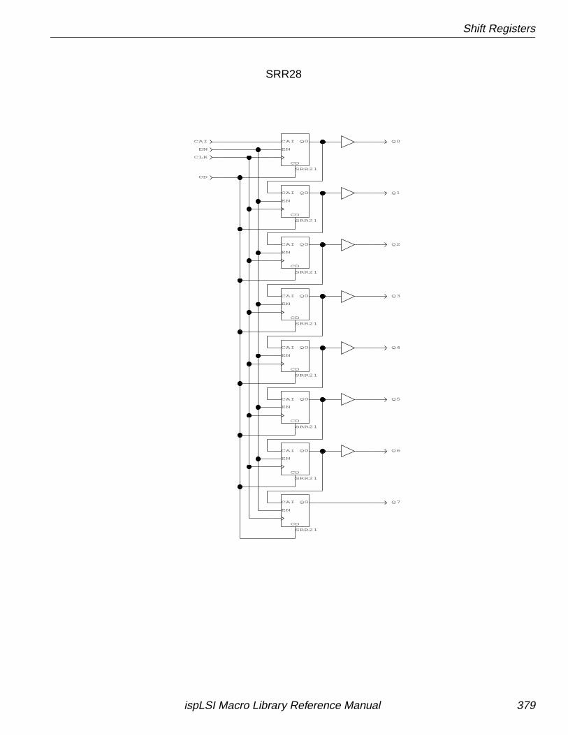
Shift Registers
CAI
Q4
Q5
Q6
Q7
CLK
CD
Q0
Q1
Q2
Q3
CAI
CD
EN
Q0
SRR21
CAI
CD
EN
Q0
SRR21
CAI
CD
EN
Q0
SRR21
CAI
CD
EN
Q0
SRR21
CAI
CD
EN
Q0
SRR21
CAI
CD
EN
Q0
SRR21
CAI
CD
EN
Q0
SRR21
CAI
CD
EN
Q0
SRR21
EN
SRR28
ispLSI Macro Library Reference Manual 379
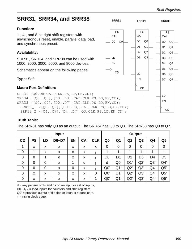
Shift Registers
SRR31, SRR34, and SRR38
Function:
1-, 4-, and 8-bit right shift registers withasynchronous reset, enable, parallel data load,and synchronous preset.
Availability:
SRR31, SRR34, and SRR38 can be used with1000, 2000, 3000, 5000, and 8000 devices.
Schematics appear on the following pages.
Type: Soft
Macro Port Definition:
SRR31 (Q0,D0,CAI,CLK,PS,LD,EN,CD);SRR34 ([Q0..Q3],[D0..D3],CAI,CLK,PS,LD,EN,CD);SRR38 ([Q0..Q7],[D0..D7],CAI,CLK,PS,LD,EN,CD);
SRR38_1 ([Q0..Q3],[D0..D3],CAI,CLK,PS,LD,EN,CD);SRR38_2 ([Q4..Q7],[D4..D7],Q3,CLK,PS,LD,EN,CD);
Truth Table:
The SRR31 has only Q0 as an output. The SRR34 has Q0 to Q3. The SRR38 has Q0 to Q7.
d = any pattern of 1s and 0s on an input or set of inputs,D0..Dn-1 = load inputs for counters and shift registers,Q0’ = previous output of flip-flop or latch, x = don’t care,↑ = rising clock edge.
Input Output
CD PS LD D0~D7 EN CAI CLK Q0 Q1 Q2 Q3 Q4 Q5
1 x x x x x x 0 0 0 0 0 00 1 x x x x ↑ 1 1 1 1 1 10 0 1 d x x ↑ D0 D1 D2 D3 D4 D50 0 0 x 1 d ↑ d Q0’ Q1’ Q2’ Q3’ Q4’0 0 0 x 0 x ↑ Q0’ Q1’ Q2’ Q3’ Q4’ Q5’0 x x x x x 0 Q0’ Q1’ Q2’ Q3’ Q4’ Q5’0 x x x x x 1 Q0’ Q1’ Q2’ Q3’ Q4’ Q5’
SRR31 SRR38SRR34
CAI
CD
D0
EN
LD
PS
Q0
CAI
CD
D0
D2
D3
EN
LD
D1
PS
Q0
Q1
Q2
Q3
CAI
CD
D0
D2
D3
D4
D5
D7
EN
LD
D6
D1
PS
Q0
Q1
Q2
Q3
Q4
Q5
Q6
Q7
ispLSI Macro Library Reference Manual 380
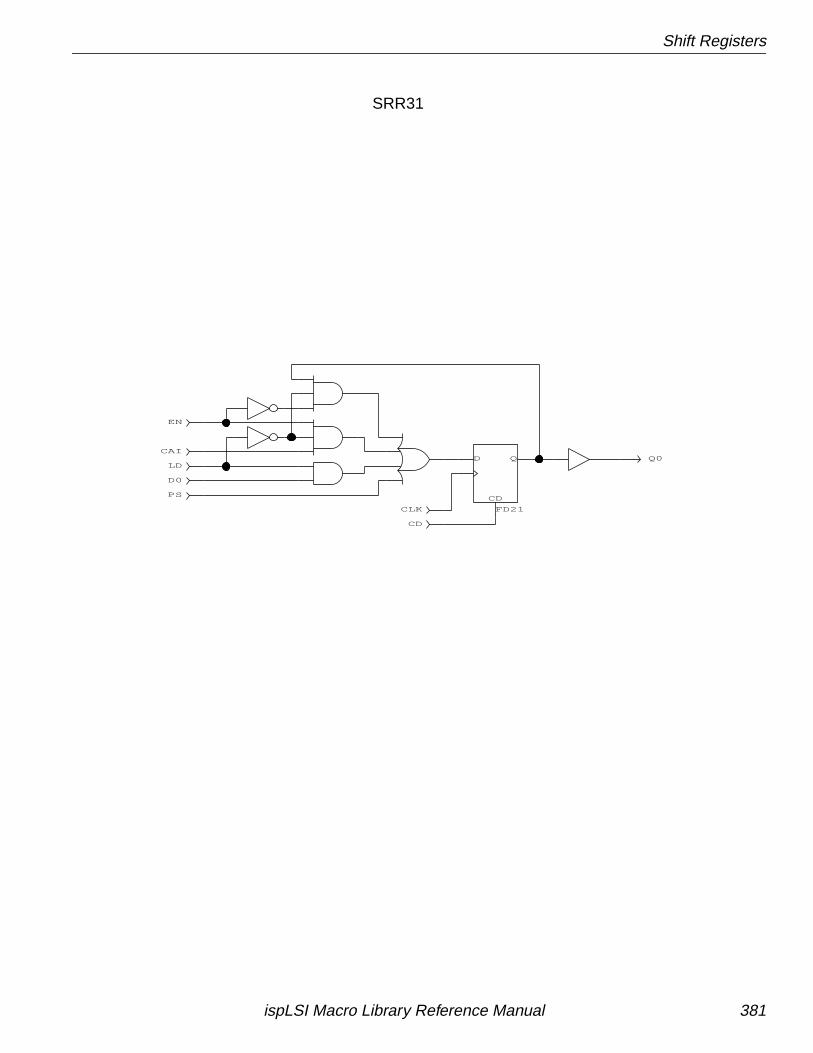
Shift Registers
Q0
CD
QD
FD21CLK
CD
LD
EN
CAI
D0
PS
SRR31
ispLSI Macro Library Reference Manual 381
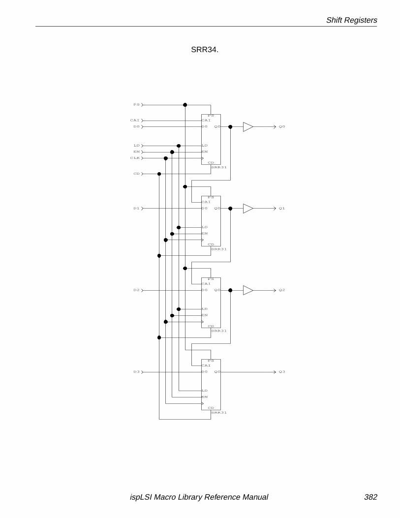
Shift Registers
D3
D2
D1
D0
LD
CD
CLK
PS
SRR31
CAI
CD
D0
EN
LD
PS
Q0
Q1
SRR31
CAI
CD
D0
EN
LD
PS
Q0
SRR31
CAI
CD
D0
EN
LD
PS
Q0
SRR31
CAI
CD
D0
EN
LD
PS
Q0 Q3
Q2
Q0
EN
CAI
SRR34.
ispLSI Macro Library Reference Manual 382
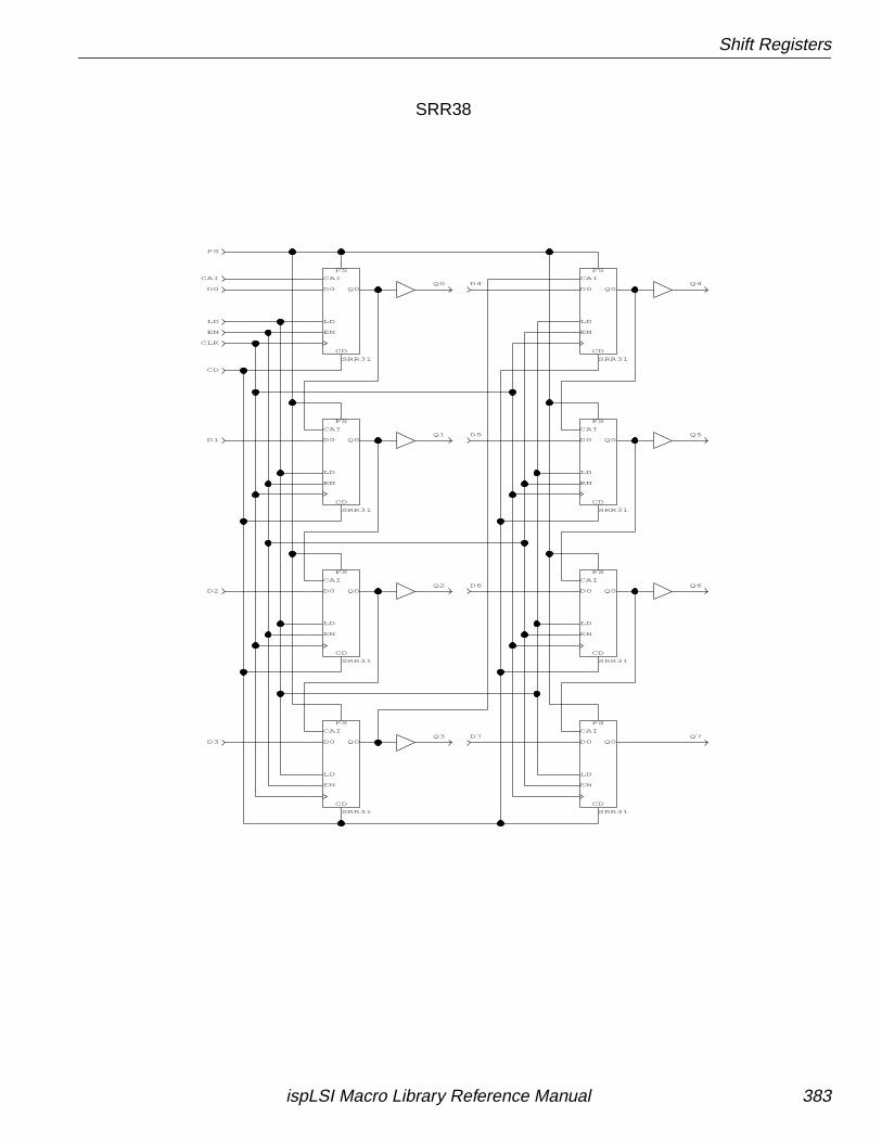
Shift Registers
Q3
Q2
Q1
Q0
SRR31
CAI
CD
D0
EN
LD
PS
Q0
Q5
SRR31
CAI
CD
D0
EN
LD
PS
Q0
SRR31
CAI
CD
D0
EN
LD
PS
Q0
SRR31
CAI
CD
D0
EN
LD
PS
Q0Q7
Q6
Q4CAI
EN
SRR31
CAI
CD
D0
EN
LD
PS
Q0
SRR31
CAI
CD
D0
EN
LD
PS
Q0
SRR31
CAI
CD
D0
EN
LD
PS
Q0
SRR31
CAI
CD
D0
EN
LD
PS
Q0
PS
CLK
CD
LD
D0
D1
D2
D3
D4
D5
D6
D7
SRR38
ispLSI Macro Library Reference Manual 383
Shift Registers
SRR41, SRR44, and SRR48
Function:
1-, 4-, and 8-bit right shift registers withsynchronous reset, enable, parallel data load,and synchronous preset.
Availability:
SRR41, SRR44, and SRR48 can be used with1000, 2000, 3000, 5000, and 8000 devices.
Schematics appear on the following pages.
Type: Soft
Macro Port Definition:
SRR41 (Q0,D0,CAI,CLK,PS,LD,EN,CS);SRR44 ([Q0..Q3],[D0..D3],CAI,CLK,PS,LD,EN,CS);SRR48 ([Q0..Q7],[D0..D7],CAI,CLK,PS,LD,EN,CS);
SRR48_1 ([Q0..Q3],[D0..D3],CAI,CLK,PS,LD,EN,CS);SRR48_2 ([Q4..Q7],[D4..D7],Q3,CLK,PS,LD,EN,CS);
Truth Table:
The SRR41 has only Q0 as an output. The SRR44 has Q0 to Q3. The SRR48 has Q0 to Q7.
d = any pattern of 1s and 0s on an input or set of inputs,D0..Dn-1 = load inputs for shift registers,Q0’ = previous output of flip-flop, x = don’t care,↑ = rising clock edge.
Input Output
PS CS LD D0~D7 EN CAI CLK Q0 Q1 Q2 Q3 Q4 Q5 Q6
1 x x x x x ↑ 1 1 1 1 1 1 10 1 x x x x ↑ 0 0 0 0 0 0 00 0 1 d x x ↑ D0 D1 D2 D3 D4 D5 D60 0 0 x 1 d ↑ d Q0’ Q1’ Q2’ Q3’ Q4’ Q5’0 0 0 x 0 x ↑ Q0’ Q1’ Q2’ Q3’ Q4’ Q5’ Q6’x x x x x x 0 Q0’ Q1’ Q2’ Q3’ Q4’ Q5’ Q6’x x x x x x 1 Q0’ Q1’ Q2’ Q3’ Q4’ Q5’ Q6’
SRR41 SRR48SRR44
CAI
CS
D0
EN
LD
PS
Q0
CAI
CS
D0
D2
D3
EN
LD
D1
PS
Q0
Q1
Q2
Q3
CAI
CS
D0
D2
D3
D4
D5
D7
EN
LD
D6
D1
PS
Q0
Q1
Q2
Q3
Q4
Q5
Q6
Q7
ispLSI Macro Library Reference Manual 384
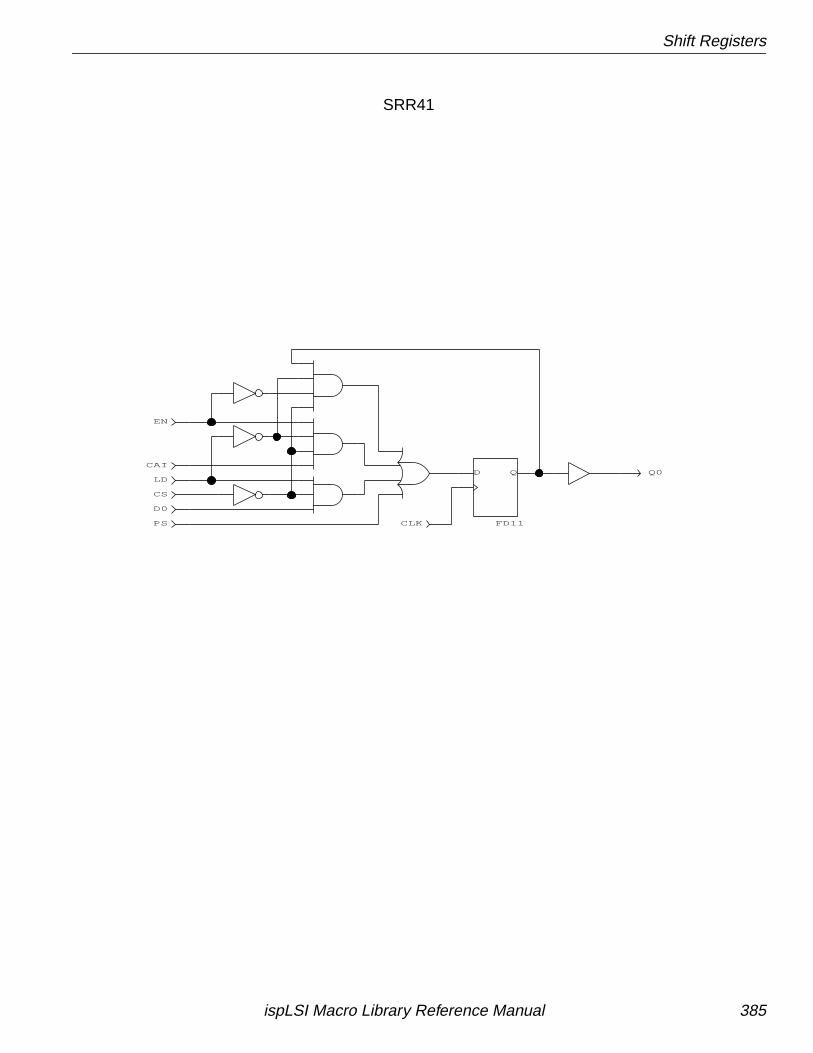
Shift Registers
Q0
CS
QD
FD11CLK
EN
CAI
LD
D0
PS
SRR41
ispLSI Macro Library Reference Manual 385
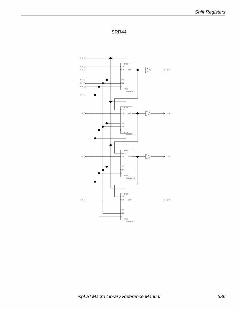
Shift Registers
SRR41
Q0
PS
LD
EN
D0
CS
CAI
SRR41
Q0
PS
LD
EN
D0
CS
CAI
SRR41
Q0
PS
LD
EN
D0
CS
CAI
SRR41
Q0
PS
LD
EN
D0
CS
CAICAI
EN
Q0
Q2
Q3
Q1
PS
CLK
CS
LD
D0
D1
D2
D3
SRR44
ispLSI Macro Library Reference Manual 386
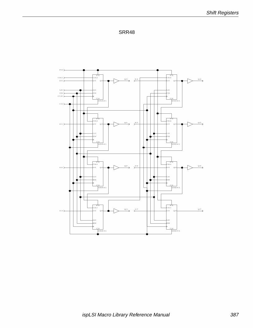
Shift Registers
SRR41
Q0
PS
LD
EN
D0
CS
CAIQ3
SRR41
Q0
PS
LD
EN
D0
CS
CAI
SRR41
Q0
PS
LD
EN
D0
CS
CAI
SRR41
Q0
PS
LD
EN
D0
CS
CAI
SRR41
Q0
PS
LD
EN
D0
CS
CAI
SRR41
Q0
PS
LD
EN
D0
CS
CAI
SRR41
Q0
PS
LD
EN
D0
CS
CAI
SRR41
Q0
PS
LD
EN
D0
CS
CAI
D7
D6
D5
D4
D3
D2
D1
D0
LD
CS
CLK
PS
Q1
Q2
Q0
EN
CAIQ4
Q6
Q7
Q5
SRR48
ispLSI Macro Library Reference Manual 387
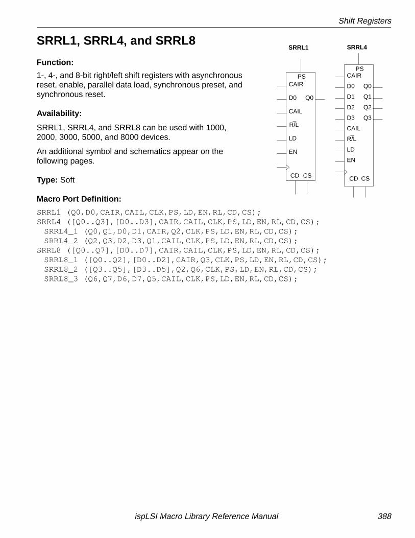
Shift Registers
SRRL1, SRRL4, and SRRL8
Function:
1-, 4-, and 8-bit right/left shift registers with asynchronousreset, enable, parallel data load, synchronous preset, andsynchronous reset.
Availability:
SRRL1, SRRL4, and SRRL8 can be used with 1000,2000, 3000, 5000, and 8000 devices.
An additional symbol and schematics appear on thefollowing pages.
Type: Soft
Macro Port Definition:
SRRL1 (Q0,D0,CAIR,CAIL,CLK,PS,LD,EN,RL,CD,CS);SRRL4 ([Q0..Q3],[D0..D3],CAIR,CAIL,CLK,PS,LD,EN,RL,CD,CS);
SRRL4_1 (Q0,Q1,D0,D1,CAIR,Q2,CLK,PS,LD,EN,RL,CD,CS);SRRL4_2 (Q2,Q3,D2,D3,Q1,CAIL,CLK,PS,LD,EN,RL,CD,CS);
SRRL8 ([Q0..Q7],[D0..D7],CAIR,CAIL,CLK,PS,LD,EN,RL,CD,CS);SRRL8_1 ([Q0..Q2],[D0..D2],CAIR,Q3,CLK,PS,LD,EN,RL,CD,CS);SRRL8_2 ([Q3..Q5],[D3..D5],Q2,Q6,CLK,PS,LD,EN,RL,CD,CS);SRRL8_3 (Q6,Q7,D6,D7,Q5,CAIL,CLK,PS,LD,EN,RL,CD,CS);
SRRL1 SRRL4
R/L
Q0
PSCAIR
LD
EN
CSCD
CAIL
D0
R/L
D0
D2
D3
CAIL
CD CS
EN
LD
CAIR
D1
PS
Q0
Q1
Q2
Q3
ispLSI Macro Library Reference Manual 388
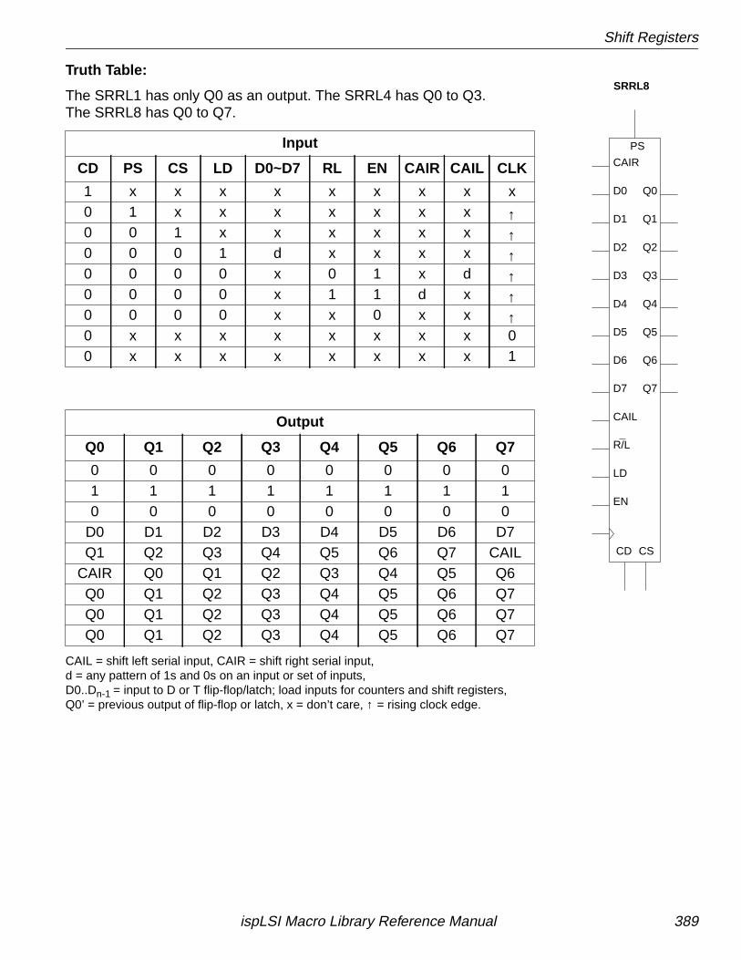
Shift Registers
Truth Table:
The SRRL1 has only Q0 as an output. The SRRL4 has Q0 to Q3.The SRRL8 has Q0 to Q7.
CAIL = shift left serial input, CAIR = shift right serial input,d = any pattern of 1s and 0s on an input or set of inputs,D0..Dn-1 = input to D or T flip-flop/latch; load inputs for counters and shift registers,Q0’ = previous output of flip-flop or latch, x = don’t care, ↑ = rising clock edge.
Input
CD PS CS LD D0~D7 RL EN CAIR CAIL CLK
1 x x x x x x x x x0 1 x x x x x x x ↑0 0 1 x x x x x x ↑0 0 0 1 d x x x x ↑0 0 0 0 x 0 1 x d ↑0 0 0 0 x 1 1 d x ↑0 0 0 0 x x 0 x x ↑0 x x x x x x x x 00 x x x x x x x x 1
Output
Q0 Q1 Q2 Q3 Q4 Q5 Q6 Q7
0 0 0 0 0 0 0 01 1 1 1 1 1 1 10 0 0 0 0 0 0 0
D0 D1 D2 D3 D4 D5 D6 D7Q1 Q2 Q3 Q4 Q5 Q6 Q7 CAIL
CAIR Q0 Q1 Q2 Q3 Q4 Q5 Q6Q0 Q1 Q2 Q3 Q4 Q5 Q6 Q7Q0 Q1 Q2 Q3 Q4 Q5 Q6 Q7Q0 Q1 Q2 Q3 Q4 Q5 Q6 Q7
SRRL8
R/L
Q7
Q6
Q5
Q4
Q3
Q2
Q1
Q0
PS
D1
CAIR
D6
LD
EN
CSCD
CAIL
D7
D5
D4
D3
D2
D0
ispLSI Macro Library Reference Manual 389
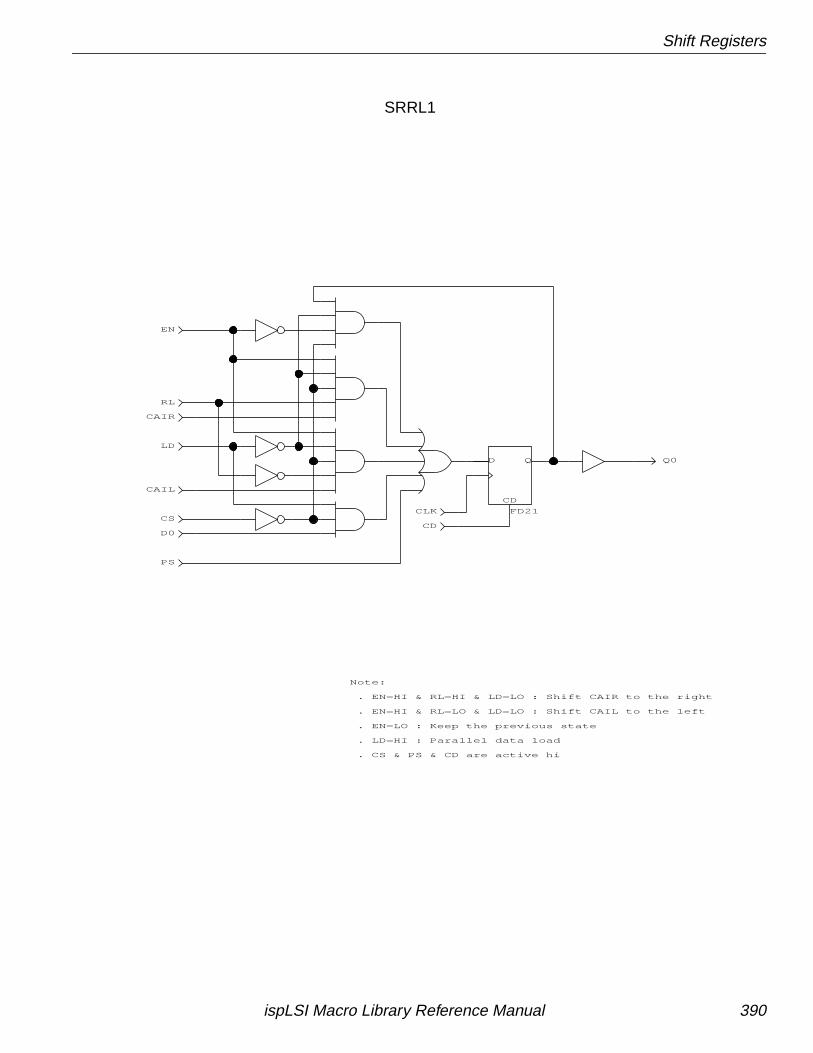
Shift Registers
Q0
EN
RL
LD
CS
. LD=HI : Parallel data load
. EN=LO : Keep the previous state
. EN=HI & RL=LO & LD=LO : Shift CAIL to the left
Note:
. CS & PS & CD are active hi
. EN=HI & RL=HI & LD=LO : Shift CAIR to the right
CAIR
CAIL
D0
PS
CD
QD
FD21CLK
CD
SRRL1
ispLSI Macro Library Reference Manual 390
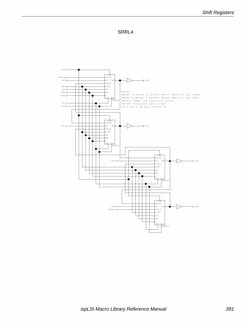
Shift Registers
CAIL
Q3
CAIR
CS
CD
CLK
EN
LD
RL
Q0
PS
CAIR
LD
EN
CSCD
CAIL
D0
SRRL1
R/L
Q0
PS
CAIR
LD
EN
CSCD
CAIL
D0
SRRL1
R/L
Q0
PS
CAIR
LD
EN
CSCD
CAIL
D0
SRRL1
R/L
PS
D0 Q0
D1 Q1
D2 Q2
D3
Note:
CS & PS & CD are active hi
EN=HI & RL=HI & LD=LO: Shift CAIR to the right
EN=HI & RL=LO & LD=LO: Shift CAIL to the left
EN=LO: Keep the previous state
LD=HI: Parallel data load
Q0
PS
CAIR
LD
EN
CSCD
CAIL
D0
SRRL1
R/L
SRRL4
ispLSI Macro Library Reference Manual 391
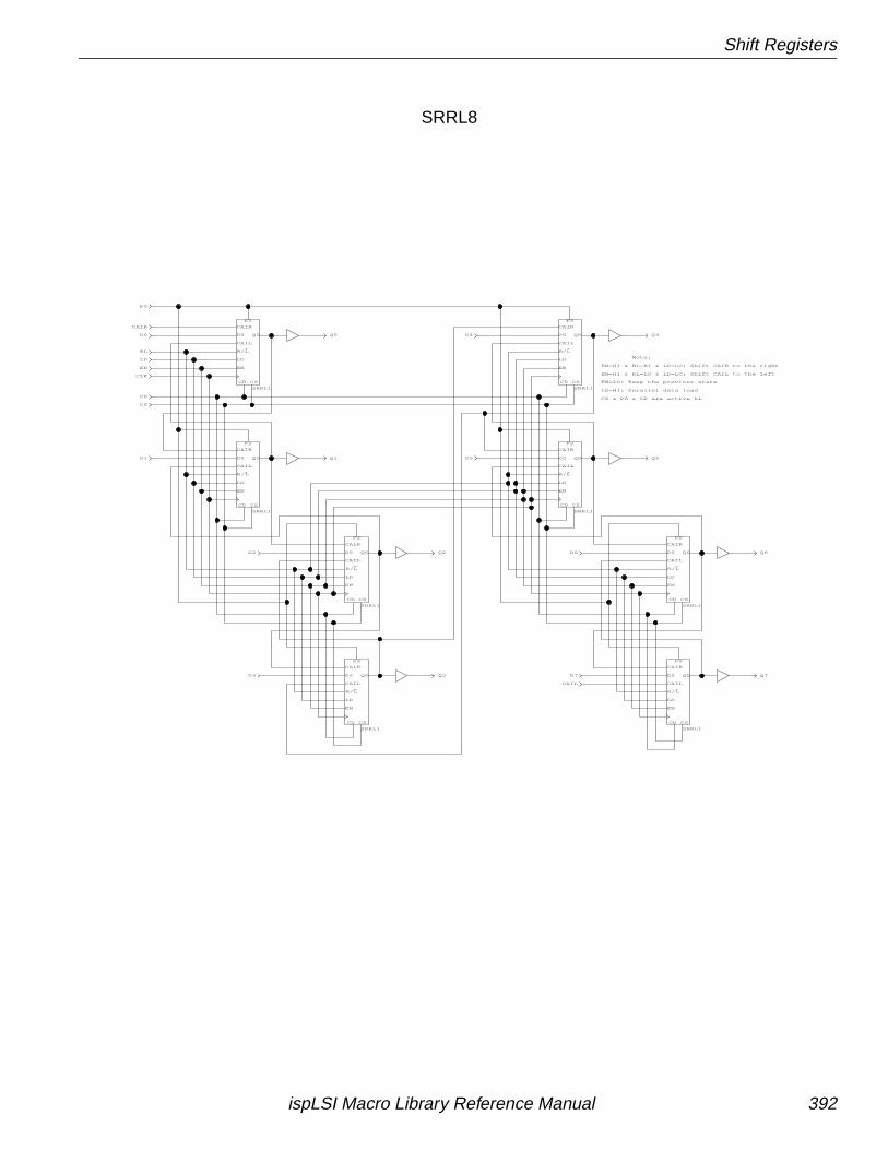
Shift Registers
CAIR
CS
CD
CLK
EN
LD
RL
Q0
PS
CAIR
LD
EN
CSCD
CAIL
D0
SRRL1
R/L
Q0
PS
CAIR
LD
EN
CSCD
CAIL
D0
SRRL1
R/L
Q0
PS
CAIR
LD
EN
CSCD
CAIL
D0
SRRL1
R/L
PS
D0 Q0
Q0
PS
CAIR
LD
EN
CSCD
CAIL
D0
SRRL1
R/L
D1 Q1
D2
D3
Q5Q0
PS
CAIR
LD
EN
CSCD
CAIL
D0
SRRL1
R/L
D5
Q2
Q3
D4 Q0
PS
CAIR
LD
EN
CSCD
CAIL
D0
SRRL1
R/L
Q4
Note:
CS & PS & CD are active hi
EN=HI & RL=HI & LD=LO: Shift CAIR to the right
EN=HI & RL=LO & LD=LO: Shift CAIL to the left
EN=LO: Keep the previous state
LD=HI: Parallel data load
CAIL
Q7
Q0
PS
CAIR
LD
EN
CSCD
CAIL
D0
SRRL1
R/L
Q0
PS
CAIR
LD
EN
CSCD
CAIL
D0
SRRL1
R/L
D6 Q6
D7
SRRL8
ispLSI Macro Library Reference Manual 392
Index
AADDF1 39ADDF16A 39ADDF2 39ADDF4 39ADDF8 39ADDF8A 39ADDH16A 54ADDH2 54ADDH3 54ADDH4 54ADDH8 54ADDH8A 54AND2 through AND18 316Arithmetic Functions 38
BBI11 284BI14 284BI18 284BI21 285BI24 285BI28 285BI31 286BI34 286BI38 286BI41 287BI44 287BI48 287Bidirectional Pins 284BIID11 288BIID14 288BIID18 288BIID21 289BIID24 289BIID28 289BIID31 290BIID34 290BIID38 290BIID41 291BIID44 291BIID48 291BIID51 292BIID54 292BIID58 292
BIID61 293BIID64 293BIID68 293BIID71 294BIID74 294BIID78 294BIID81 295BIID84 295BIID88 295BIIL11 296BIIL14 296BIIL18 296BIIL21 297BIIL24 297BIIL28 297BIIL31 298BIIL34 298BIIL38 298BIIL41 299BIIL44 299BIIL48 299BIIL51 300BIIL54 300BIIL58 300BIIL61 301BIIL64 301BIIL68 301BIIL71 302BIIL74 302BIIL78 302BIIL81 303BIIL84 303BIIL88 303BIN27 104Binary Counters 113BUF 317
CCBD11 113CBD12 113CBD14 113CBD18 113CBD21 119CBD22 119CBD24 119
ispLSI Macro Library Reference Manual 393
Index
CBD28 119CBD31 125CBD32 125CBD34 125CBD38 125CBD41 132CBD42 132CBD44 132CBD48 132CBD516 139CBD616 139CBU11 149CBU12 149CBU14 149CBU18 149CBU21 155CBU22 155CBU24 155CBU28 155CBU31 161CBU32 161CBU34 161CBU38 161CBU41 168CBU42 168CBU44 168CBU48 168CBU516 175CBU616 175CBU716 184CBUD1 190CBUD2 190CBUD4 190CBUD8 190CDD14 200CDD18 200CDD24 206CDD28 206CDD34 212CDD38 212CDD44 218CDD48 218CDU14 222CDU18 222CDU24 228CDU28 228CDU34 234CDU38 234CDU44 240CDU48 240CDUD4 246CDUD4c 256
CDUD8 246CDUD8c 256CGD14 266CGD24 269CGU14 272CGU24 276CGUD4 279CMP2 67CMP4 67CMP8 67Coders 103Comparators 67Counters 112
DD Flip-flops 347D Latches 361DEC2 106DEC2E 106DEC3 107DEC3E 107DEC4 108DEC4E 108Decade Counters 200Decoders 104Demultiplexers 339DMUX2 339DMUX22 341DMUX22E 341DMUX24 342DMUX24E 342DMUX2E 339DMUX4 340DMUX42 343DMUX42E 343DMUX44 344DMUX44E 344DMUX4E 340DMUX82 345DMUX82E 345Documentation Conventions 8
EEncoders 109
FF3ADD 39F3SUB 80FD11 347FD14 347FD18 347FD21 348
ispLSI Macro Library Reference Manual 394
Index
FD24 348FD28 348FD31 349FD34 349FD38 349FD41 350FD44 350FD48 350FD51 351FD54 351FD58 351FD61 352FD64 352FD68 352FD71 353FD74 353FD78 353FD81 354FD84 354FD88 354FD91 355FD94 355FD98 355FDA1 356FDA4 356FDA8 356FJK11 357FJK21 357FJK31 358FJK41 358FJK51 359FT11 360FT21 360
GGray Code Counters 266
II/O Pins 283IB11 304ID11 305ID14 305ID18 305ID21 306ID24 306ID28 306IL11 307IL14 307IL18 307IL21 308IL24 308IL28 308
Input Pins 304INV 317
JJK Flip-flops 357
LLD11 361LD14 361LD18 361LD21 362LD24 362LD28 362LD31 363LD34 363LD38 363LD41 364LD44 364LD48 364LD51 365LD54 365LD58 365LD61 366LD64 366LD68 366LD71 367LD74 367LD78 367LD81 368LD84 368LD88 368LD91 369LD94 369LD98 369LDA1 370LDA4 370LDA8 370Logic Gates 315, 316Logic Resources 14LSR1 371LSR2 371LXOR 322
MMAG2 68MAG4 68MAG8 68Module Macro Truth Tables 12MULT24 70MULT44 70Multiplexers 324Multipliers 70
ispLSI Macro Library Reference Manual 395
Index
MUX/DMUX 323MUX16 327MUX16E 327MUX2 324MUX22 331MUX22E 331MUX24 332MUX24E 332MUX2E 324MUX4 325MUX42 333MUX42E 333MUX44 334MUX44AE 335MUX44E 334MUX4E 325MUX8 326MUX82 338MUX82E 338MUX8E 326
NNAND16 318NAND2 through NAND12 318NOR16 319NOR2 through NOR12 319
OOB11 309OB21 310OB24 310OB28 310OR16 320OR2 through OR12 320OT11 311OT14 311OT18 311OT21 312OT24 312OT28 312OT31 313OT34 313OT38 313OT41 314OT44 314OT48 314Output Pins 309Overview 7
PPG1 74PG2 74PG3 74PG4 74Pin Labeling 13Preface 7PREN10 110PREN10E 110PREN16 111PREN16E 111PREN8 109PREN8E 109Propagate-Generate 74Purpose and Scope 8
RRegisters 346
SShift Registers 372Signal Names 9SR Latches 371SRR11 372SRR14 372SRR18 372SRR21 376SRR24 376SRR28 376SRR31 380SRR34 380SRR38 380SRR41 384SRR44 384SRR48 384SRRL1 388SRRL4 388SRRL8 388SUBF1 80SUBF16A 80SUBF2 80SUBF4 80SUBF8 80SUBF8A 80SUBH1 90SUBH16A 90SUBH2 90SUBH3 90
ispLSI Macro Library Reference Manual 396
Index
SUBH4 90SUBH8 90SUBH8A 90Subtractors 80
TToggle Flip-flops 360Truth Tables 11
UUsing the NOMIN Attribute 15
XXNOR2 321XNOR3 321XNOR4 321XNOR7 321XNOR8 321XNOR9 321XOR2 322XOR3 322XOR4 322XOR8 322XOR9 322
ispLSI Macro Library Reference Manual 397