Embed Size (px)
Citation preview

Kinetis MCUsSecuring the Internet of Tomorrow
freescalecomSecurity
Security and Integrity Solutions
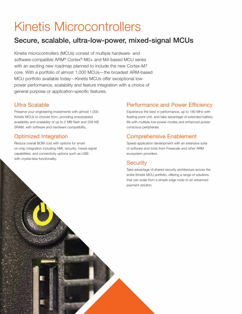
Kinetis MicrocontrollersSecure scalable ultra-low-power mixed-signal MCUs
Kinetis microcontrollers (MCUs) consist of multiple hardware- and software-compatible ARMreg Cortexreg-M0+ and M4-based MCU series with an exciting new roadmap planned to include the new Cortex-M7 core With a portfolio of almost 1000 MCUsmdashthe broadest ARM-based MCU portfolio available todaymdashKinetis MCUs offer exceptional low-power performance scalability and feature integration with a choice of general purpose or application-specific features
Ultra ScalablePreserve your engineering investments with almost 1000
Kinetis MCUs to choose from providing unsurpassed
availability and scalability of up to 2 MB flash and 256 KB
SRAM with software and hardware compatibility
Optimized IntegrationReduce overall BOM cost with options for smart
on-chip integration including HMI security mixed-signal
capabilities and connectivity options such as USB
with crystal-less functionality
Performance and Power EfficiencyExperience the best in performance up to 180 MHz with
floating point unit and take advantage of extended battery
life with multiple low-power modes and enhanced power-
conscious peripherals
Comprehensive EnablementSpeed application development with an extensive suite
of software and tools from Freescale and other ARM
ecosystem providers
Security Take advantage of shared security architecture across the
entire Kinetis MCU portfolio offering a range of solutions
that can scale from a simple edge node to an advanced
payment solution
2freescalecomKinetis
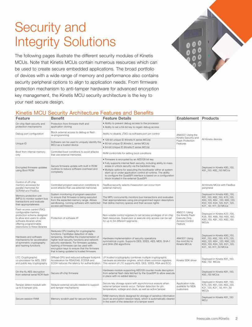
The following pages illustrate the different security modules of Kinetis MCUs Note that Kinetis MCUs contain numerous resources which can be used to create secure embedded applications The broad portfolio of devices with a wide range of memory and performance also contains security peripheral options to align to application needs From firmware protection mechanism to anti-tamper hardware for advanced encryption key management the Kinetis MCU security architecture is the key to your next secure design
Security and Integrity Solutions
Kinetis MCU Security Architecture Features and BenefitsFeature Benefit Feature Details Enablement ProductsOn-chip flash security and protection mechanisms
Protection from firmware theft and application cloning
bull Ability to prevent debug access to the processor
bull Ability to set a 64-bit key to regain debug access
AN4507 Using the Kinetis Security and Flash Protection Features
All Kinetis devices
Debug port configuration Block external access to debug or flash re-programming Ability to disable JTAG via software port pin control
Unique ID Software can be used to uniquely identify the MCU as a trusted device
bull 128-bit unique ID (Kinetis K series MCUs)
bull 80-bit unique ID (Kinetis L series MCUs)
bull 64-bit Unique ID (Kinetis E series MCUs)
Boot from internal memory only
Controlled boot conditions to avoid attacks that use external memories NVM control bits for setting boot conditions
Encrypted firmware updates using Boot ROM
Secure firmware update with built in ROM routines to reduce software overhead and complexity
bull Firmware is encrypted by an AES128 bit key
bull Fully supports internal flash security including ability to mass erase or unlock security via the backdoor key
bull Multiple options for executing the bootloader either at system start-up or under application control at runtime The ability to configure the QuadSPI interface is based on a configuration block located in the external QuadSPI
Deployed in Kinetis K80_150 K81_150 K82_150 MCUs
Control of off-chip memory accesses for parallel memories for SDRAM and FlexBus
Controlled program execution conditions to avoid attacks that use external memories
FlexBus security selects if execution can occur from external memory
All Kinetis MCUs with FlexBus peripheral
Memory protection unit (MPU) to monitor system bus transactions and evaluate their appropriateness
System monitoring of program execution to ensure that firmware is being executed from the expected memory range Allows sandboxing running software with restricted access permissions
The MPU concurrently monitors bus transactions and evaluates their appropriateness using pre-programmed region descriptors that define memory spaces and their access rights
Deployed in Kinetis K80_150 K81_150 K82_150 K70_120 K63_120 K64 _120 K60_120 K53_100 K24_120 K21_120 K21_ 50 K11_50 MCUs
Flash access control (FAC) configurable memory protection scheme designed to allow end users to utilize software libraries while offering programmable restrictions to these libraries
Protection of software IPNon-volatile control registers to set access privileges of on chip flash resources Supervisor or execute only access can be set for up to 64 different segments
AN5211 Using the Kinetis Flash Execute-Only Access Control Feature
Deployed in Kinetis K22_100 K26_180 K66_180 K65_180 K80_150 K81_150 K82_150 MCUs
Hardware and software mechanisms for acceleration of symmetric cryptography and hashing functions
Reduces CPU loading for cryptographic functions Facilitates detection of data tampering Simplifies the implementation of higher level security functions and network security standards For firmware updates hashing of firmware can be used with encryption keys to ensure that the firmware that is being updated is trusted firmware
Hardware implementation of security operations symmetrical crypto Supports DES 3DES AES MD5 SHA-1 and SHA-256 algorithms
AN4307 Using the mmCAU in Kinetis MCUs
Deployed in Kinetis K80_150 K81_150 K82_150 K70_120 K63_120 K64 _120 K60_120 K53_100 K24_120 K21_120 K21_ 50 K11_50 MCUs
LTC Cryptographic co-processor for AES DES and public key cryptography
Offload CPU and reduced software footprint Acceleration for RSA2048 ECDSA and ECDH reduces the latency for authentication
LP trusted cryptography combines multiple cryptographic hardware accelerator engines which share common registers This version of LTC supports AES DES 3DES RSA and ECC
Kinetis SDK driver Deployed in Kinetis K81_150 K82_150 MCUs
On-the-fly AES decryption from external serial NOR flash Secure off-chip firmware
Hardware module supporting AES128 counter mode decryption from external flash data fetched by the QuadSPI to allow execute in place with no added latency
Deployed in Kinetis K81_150 K82_150 MCUs
Tamper detect module with up to 8 tamper pins
Reduce external circuits needed to support anti-tamper mechanisms
Secure key storage space with asynchronous erasure when external tamper events occur Tamper detection for pin temperature voltage and clock as well as active tamper
Application note available for NDA customers
Deployed in Kinetis K81_150 K70_120 K61_120 K63_120 K21_120 K21_ 50 K11_50 MCUs
Secure session RAM Memory scratch pad for secure functionsRAM memory block designed for storage of sensitive information (such as encryption session keys) which is automatically cleared in the event of the detection of a tamper event
Deployed in Kinetis K81_150 MCU
3 Security and Integrity Solutions
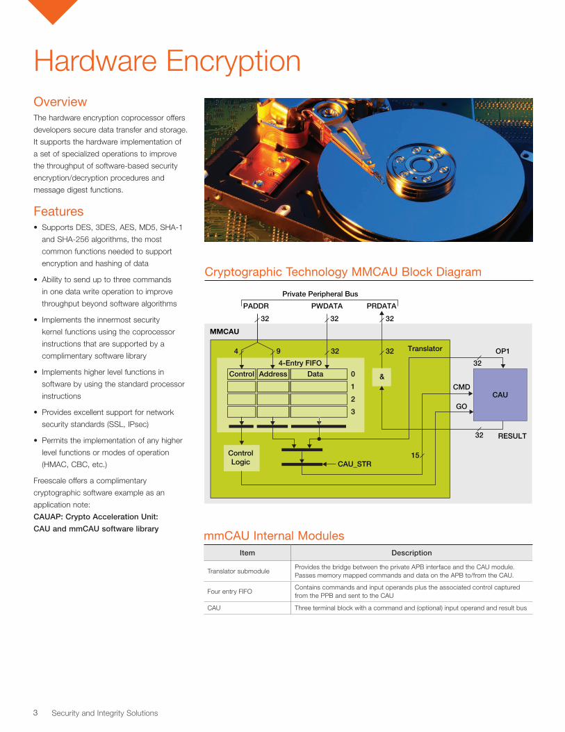
OverviewThe hardware encryption coprocessor offers
developers secure data transfer and storage
It supports the hardware implementation of
a set of specialized operations to improve
the throughput of software-based security
encryptiondecryption procedures and
message digest functions
Featuresbull Supports DES 3DES AES MD5 SHA-1
and SHA-256 algorithms the most
common functions needed to support
encryption and hashing of data
bull Ability to send up to three commands
in one data write operation to improve
throughput beyond software algorithms
bull Implements the innermost security
kernel functions using the coprocessor
instructions that are supported by a
complimentary software library
bull Implements higher level functions in
software by using the standard processor
instructions
bull Provides excellent support for network
security standards (SSL IPsec)
bull Permits the implementation of any higher
level functions or modes of operation
(HMAC CBC etc)
Freescale offers a complimentary
cryptographic software example as an
application note
CAUAP Crypto Acceleration Unit
CAU and mmCAU software library
Hardware Encryption
Cryptographic Technology MMCAU Block Diagram
mmCAU Internal ModulesItem Description
Translator submoduleProvides the bridge between the private APB interface and the CAU module Passes memory mapped commands and data on the APB tofrom the CAU
Four entry FIFOContains commands and input operands plus the associated control captured from the PPB and sent to the CAU
CAU Three terminal block with a command and (optional) input operand and result bus
Cryptographic Technology mmCAU Block Diagram
Translator
Private Peripheral Bus
PADDR
MMCAU
32 32 32
32
32
32
15
RESULT
CAU_STR
ControlLogic
Control Address Data
4-Entry FIFO
1
0
2
3
ampCMD
GO
CAU
OP13294
PWDATA PRDATA
4freescalecomKinetis
Kinetis MCUs
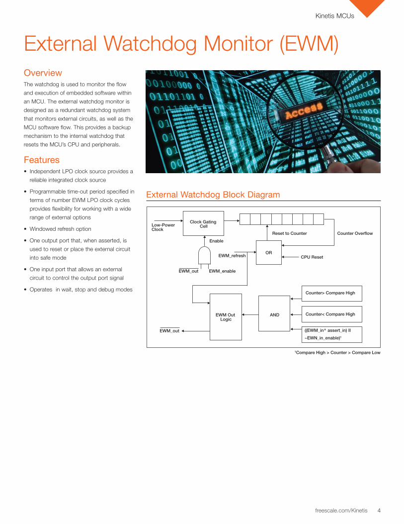
External Watchdog Monitor (EWM)
External Watchdog Block DiagramExternal Watchdog Block Diagram
EWM Out Logic
AND
OR
Countergt Compare High
Counterlt Compare High
((EWM_in^ assert_in) II
~EWN_in_enable)1
EWM_out
1Compare High gt Counter gt Compare Low
EWM_out
Enable
Low-PowerClock
Clock Gating Cell
EWM_enable
EWM_refresh
Reset to Counter
CPU Reset
Counter Overflow
OverviewThe watchdog is used to monitor the flow
and execution of embedded software within
an MCU The external watchdog monitor is
designed as a redundant watchdog system
that monitors external circuits as well as the
MCU software flow This provides a backup
mechanism to the internal watchdog that
resets the MCUrsquos CPU and peripherals
Featuresbull Independent LPO clock source provides a
reliable integrated clock source
bull Programmable time-out period specified in
terms of number EWM LPO clock cycles
provides flexibility for working with a wide
range of external options
bull Windowed refresh option
bull One output port that when asserted is
used to reset or place the external circuit
into safe mode
bull One input port that allows an external
circuit to control the output port signal
bull Operates in wait stop and debug modes
5 Security and Integrity Solutions
Memory Protection Unit
Memory Protection Unit Block DiagramMemory Protection Unit Block Diagram
RegionDescriptor X
RegionDescriptor 1
RegionDescriptor 0
AccessEvaluation
Macro
Slave Port nAddress Phase SIgnals
InternalPeripheral Bus
AccessEvaluation
Macro
AccessEvaluation
Macro
Mux
MPU_EARn MPU_EDRn
OverviewThe memory protection unit concurrently
monitors system bus transactions and
evaluates their appropriateness using pre-
programmed region descriptors that define
memory spaces and their access rights
Memory references that have sufficient
access control rights are allowed to complete
while references that are not mapped to any
region descriptor or have insufficient rights are
terminated with a protection error response
Featuresbull Up to 16 program-visible 128-bit region
descriptors provide maximum flexibility for
software management of multiple layers of
access control
bull Read write execute attributes can be set
bull Hardware-assisted maintenance of the
descriptor valid bit minimizes coherency
issues
bull Detects access protection errors if a
memory reference does not hit in any
memory region or if the reference is illegal
in all hit memory regions If an access error
occurs the reference is terminated with an
error response and the memory protection
unit inhibits the bus cycle being sent to the
targeted slave device
bull Error registers (per slave port) capture the
last faulting address attributes and other
information for traceability of faults
bull Global memory protection unit enable
disable control bit for easy control
6freescalecomKinetis
Kinetis MCUs
Tamper DetectOverviewThe tamper detect module provides secure
key storage with internalexternal tamper
detect for unsecure flash temperature
clock supply voltage variations and physical
attack detection
Featuresbull Independent power supply POR and
32 KHz oscillator
bull 32 bytes of secure storage reset on
tamper detect
bull Tamper time register records time of
tamper detect
bull Two active tamper shift registers each
with configurable polynomial
bull Register protection
bull Up to 10 internal tamper sources
including time counter overflow voltage
temperature and clock out-of-range flash
security disable and test mode entry and
optional DryIce and security module
bull Up to eight external tamper pins capable
of generating interrupt or tamper event
bull Configurable polarity and digital glitch
filter with optional prescaler
bull Configurable for either static or active
tamper input
bull Supports software-initiated tamper pin
assertion
DryIce Tamper Detect Module
VBAT P
OR
Test
Mode F
lag
Flash
Securi
ty Fla
g
Time O
verflo
w Flag
Monoto
nic O
verflo
w Flag
Volta
ge Ta
mper F
lag
Clock T
amper
Flag
Tempera
ture T
amper
Flag
Software
Write
to D
RY_TSR
Tamper
Pin Fla
g
Securi
ty Ta
mper Fla
g
DryIce Tamper Flag (DTF) g 1
32-byte Security Key Erased Timeof Tamper Recorded in RTC_TTSR
Optional RTC Interrupt andWakeup Pin Assertion
OptionallySet TIF
Optional Chip Reset
Optional DryIce Interrupt
Additional 128-byteAdditional Secure RAM (optional for K65_180 and K81_150)
2 KB Secure Session RAM (optional for
K81_150)
7 Security and Integrity Solutions
Random Number GeneratorOverviewThere are two types of random number
generators available with Kinetis MCUs
The first of which is the random number
generator accelerator which is a digital
integrated circuit capable of generating
32-bit random numbers
bull The random bits are generated by
clocking shift registers with clocks derived
from ring oscillators
bull The configuration of the shift registers
ensures statistically good data
bull The oscillators with their unknown
frequencies provide the required entropy
needed to create random data
It is highly recommended to use the random
data produced by this module as an input
seed to a NIST approved pseudo random
number generator
The second random number generator
available with the Kinetis K8x MCU family
is the stand-alone true random number
generator or SA-TRNG The SA-TRNG is
hardware accelerator module that generates
a 512-bit entropy as needed by an entropy
consuming module or by other post
processing functions
The entropy generated by an TRNG is
intended for direct use by functions that
generate secret keys per-message secrets
random challenges and other similar
quantities used in cryptographic algorithms
TRNG is based on collecting bits from a
random noise source This random noise
source is a ring oscillator that is sensitive to
random noise (temperature variations voltage
variations cross-talk and other random noise)
within the device in which the TRNG is used
TRNG can be used to seed a hardware or
software based implementation of a DRBG
defined by SP800-90
Stand-Alone True Random Number Generator (SA-TRNG)Stand-Alone True Random Number Generator Block Diagram
SA-RNG-WRAPPER
OSC
TRNG
INTERFACE
SA-RNG
8freescalecomKinetis
Kinetis MCUs
LP Trusted Crypto (LTC)
LP Trusted Crypto (LTC) Block Diagram LP Trusted Crypto (LTC) Block Diagram
LTC
Slave interface
Interrupt
LTC Registers
AES
System clock
Async reset
Sync reset
Input FIFO
Output FIFO
DES
PKHA
OverviewLP trusted cryptography combines multiple
cryptographic hardware accelerator engines
that share common registers This version
of LTC supports AES DES 3DES RSA
and ECC
Featuresbull AES128 and AES256 support and
support for
Confidentiality (ECB CBC CTR OFB
CFB128)
Authenticated confidentiality (CCM)
Authentication (XCBC-MAC CMAC)
bull Single- and triple-DES functionality and
ECB CBC CFB and OFB modes as well
as key parity checking in compliance with
the DES specification
bull Public key hardware accelerator capable of
performing a number of different operations
used in public-key cryptography including
modular arithmetic functions such as
addition subtraction multiplication
exponentiation reduction and inversion
as well as elliptic curve functions for
point addition point doubling and point
multiplication
Software Enablementbull The LTC driver is provided in the
Kinetis SDK
Support for symmetric and asymmetric
modes
Public key cryptography support
- RSA ECDSA ECDH
9 Security and Integrity Solutions
On-The-Fly AES Decryption Module (OTFAD)
On-The-Fly AES Decryption Module (OTFAD) Block Diagram On-The-Fly AES Decryption Module (OTFAD) Block Diagram
On-the-fly AESDecryption Engine
(OTFAD)
Quad SPI Controller
Counter
Quad SPIMemory
Quad SPIReceiveBuffer Encrypted Code
Cipher Text
Plain Text
System Interconnect
Data in clear
N Bytes Buffer
AES CTREngine
Featuresbull On-the-fly decryption module is combined
with an external flash memory controller
known as the QuadSPI to support
interfacing to encrypted external serial NOR
flash memory
bull Combined access speed of QuadSPI
coupled with internal processor-local cache
memories allow the application code to be
executed directly from the external memory
without the need to copy the code into
another (faster) memory
bull The OTFAD engine implements a block
cipher mode of operation specifically
supporting the counter mode (CTR)
bull OTFAD engine post decryption transfers
the data in clear back to QuadSPI Rx
buffer that is then available for the system
bull Hardware support available for four
independent decryption segments known
as memory context
Each context has a unique 128-bit
key 64-bit counter and 64-bit memory
region descriptor
For more information please visit freescalecomSecurity
Freescale the Freescale logo CodeWarrior ColdFire ColdFire+ Kinetis PEG Processor Expert and Xtrinsic are trademarks of Freescale Semiconductor Inc Reg US Pat amp Tm Off Tower is a trademark of Freescale Semiconductor Inc All other product or service names are the property of their respective owners ARM Cortex and Keil are registered trademarks of ARM Limited (or its subsidiaries) in the EU andor elsewhere All rights reserved copy 2012 2014-2015 Freescale Semiconductor Inc
Document Number BRKINETISSECSOLS REV 2
ResourcesProduct PagesfreescalecomKinetisKseries
Kinetis K8x MCU Family
Kinetis K7x MCU Family
Kinetis K6x MCU Family
Kinetis K2x MCU Family
Kinetis K1x MCU Family
Freescale Freedom Development PlatformfreescalecomFreedom
Tower System Modular Development PlatformfreescalecomTower
Software Development Kit for Kinetis MCUsfreescalecomKSDK
Complimentary USB Stack with Personal Healthcare Device and USB Audio ClassesfreescalecomUSB
Sensor Fusion Solutionshttpwwwfreescalecomsensorfusion
Freescale Touch SoftwarewwwfreescalecomTouchSW
Security and Integrity Solutions
Kinetis MicrocontrollersSecure scalable ultra-low-power mixed-signal MCUs
Kinetis microcontrollers (MCUs) consist of multiple hardware- and software-compatible ARMreg Cortexreg-M0+ and M4-based MCU series with an exciting new roadmap planned to include the new Cortex-M7 core With a portfolio of almost 1000 MCUsmdashthe broadest ARM-based MCU portfolio available todaymdashKinetis MCUs offer exceptional low-power performance scalability and feature integration with a choice of general purpose or application-specific features
Ultra ScalablePreserve your engineering investments with almost 1000
Kinetis MCUs to choose from providing unsurpassed
availability and scalability of up to 2 MB flash and 256 KB
SRAM with software and hardware compatibility
Optimized IntegrationReduce overall BOM cost with options for smart
on-chip integration including HMI security mixed-signal
capabilities and connectivity options such as USB
with crystal-less functionality
Performance and Power EfficiencyExperience the best in performance up to 180 MHz with
floating point unit and take advantage of extended battery
life with multiple low-power modes and enhanced power-
conscious peripherals
Comprehensive EnablementSpeed application development with an extensive suite
of software and tools from Freescale and other ARM
ecosystem providers
Security Take advantage of shared security architecture across the
entire Kinetis MCU portfolio offering a range of solutions
that can scale from a simple edge node to an advanced
payment solution
2freescalecomKinetis
The following pages illustrate the different security modules of Kinetis MCUs Note that Kinetis MCUs contain numerous resources which can be used to create secure embedded applications The broad portfolio of devices with a wide range of memory and performance also contains security peripheral options to align to application needs From firmware protection mechanism to anti-tamper hardware for advanced encryption key management the Kinetis MCU security architecture is the key to your next secure design
Security and Integrity Solutions
Kinetis MCU Security Architecture Features and BenefitsFeature Benefit Feature Details Enablement ProductsOn-chip flash security and protection mechanisms
Protection from firmware theft and application cloning
bull Ability to prevent debug access to the processor
bull Ability to set a 64-bit key to regain debug access
AN4507 Using the Kinetis Security and Flash Protection Features
All Kinetis devices
Debug port configuration Block external access to debug or flash re-programming Ability to disable JTAG via software port pin control
Unique ID Software can be used to uniquely identify the MCU as a trusted device
bull 128-bit unique ID (Kinetis K series MCUs)
bull 80-bit unique ID (Kinetis L series MCUs)
bull 64-bit Unique ID (Kinetis E series MCUs)
Boot from internal memory only
Controlled boot conditions to avoid attacks that use external memories NVM control bits for setting boot conditions
Encrypted firmware updates using Boot ROM
Secure firmware update with built in ROM routines to reduce software overhead and complexity
bull Firmware is encrypted by an AES128 bit key
bull Fully supports internal flash security including ability to mass erase or unlock security via the backdoor key
bull Multiple options for executing the bootloader either at system start-up or under application control at runtime The ability to configure the QuadSPI interface is based on a configuration block located in the external QuadSPI
Deployed in Kinetis K80_150 K81_150 K82_150 MCUs
Control of off-chip memory accesses for parallel memories for SDRAM and FlexBus
Controlled program execution conditions to avoid attacks that use external memories
FlexBus security selects if execution can occur from external memory
All Kinetis MCUs with FlexBus peripheral
Memory protection unit (MPU) to monitor system bus transactions and evaluate their appropriateness
System monitoring of program execution to ensure that firmware is being executed from the expected memory range Allows sandboxing running software with restricted access permissions
The MPU concurrently monitors bus transactions and evaluates their appropriateness using pre-programmed region descriptors that define memory spaces and their access rights
Deployed in Kinetis K80_150 K81_150 K82_150 K70_120 K63_120 K64 _120 K60_120 K53_100 K24_120 K21_120 K21_ 50 K11_50 MCUs
Flash access control (FAC) configurable memory protection scheme designed to allow end users to utilize software libraries while offering programmable restrictions to these libraries
Protection of software IPNon-volatile control registers to set access privileges of on chip flash resources Supervisor or execute only access can be set for up to 64 different segments
AN5211 Using the Kinetis Flash Execute-Only Access Control Feature
Deployed in Kinetis K22_100 K26_180 K66_180 K65_180 K80_150 K81_150 K82_150 MCUs
Hardware and software mechanisms for acceleration of symmetric cryptography and hashing functions
Reduces CPU loading for cryptographic functions Facilitates detection of data tampering Simplifies the implementation of higher level security functions and network security standards For firmware updates hashing of firmware can be used with encryption keys to ensure that the firmware that is being updated is trusted firmware
Hardware implementation of security operations symmetrical crypto Supports DES 3DES AES MD5 SHA-1 and SHA-256 algorithms
AN4307 Using the mmCAU in Kinetis MCUs
Deployed in Kinetis K80_150 K81_150 K82_150 K70_120 K63_120 K64 _120 K60_120 K53_100 K24_120 K21_120 K21_ 50 K11_50 MCUs
LTC Cryptographic co-processor for AES DES and public key cryptography
Offload CPU and reduced software footprint Acceleration for RSA2048 ECDSA and ECDH reduces the latency for authentication
LP trusted cryptography combines multiple cryptographic hardware accelerator engines which share common registers This version of LTC supports AES DES 3DES RSA and ECC
Kinetis SDK driver Deployed in Kinetis K81_150 K82_150 MCUs
On-the-fly AES decryption from external serial NOR flash Secure off-chip firmware
Hardware module supporting AES128 counter mode decryption from external flash data fetched by the QuadSPI to allow execute in place with no added latency
Deployed in Kinetis K81_150 K82_150 MCUs
Tamper detect module with up to 8 tamper pins
Reduce external circuits needed to support anti-tamper mechanisms
Secure key storage space with asynchronous erasure when external tamper events occur Tamper detection for pin temperature voltage and clock as well as active tamper
Application note available for NDA customers
Deployed in Kinetis K81_150 K70_120 K61_120 K63_120 K21_120 K21_ 50 K11_50 MCUs
Secure session RAM Memory scratch pad for secure functionsRAM memory block designed for storage of sensitive information (such as encryption session keys) which is automatically cleared in the event of the detection of a tamper event
Deployed in Kinetis K81_150 MCU
3 Security and Integrity Solutions
OverviewThe hardware encryption coprocessor offers
developers secure data transfer and storage
It supports the hardware implementation of
a set of specialized operations to improve
the throughput of software-based security
encryptiondecryption procedures and
message digest functions
Featuresbull Supports DES 3DES AES MD5 SHA-1
and SHA-256 algorithms the most
common functions needed to support
encryption and hashing of data
bull Ability to send up to three commands
in one data write operation to improve
throughput beyond software algorithms
bull Implements the innermost security
kernel functions using the coprocessor
instructions that are supported by a
complimentary software library
bull Implements higher level functions in
software by using the standard processor
instructions
bull Provides excellent support for network
security standards (SSL IPsec)
bull Permits the implementation of any higher
level functions or modes of operation
(HMAC CBC etc)
Freescale offers a complimentary
cryptographic software example as an
application note
CAUAP Crypto Acceleration Unit
CAU and mmCAU software library
Hardware Encryption
Cryptographic Technology MMCAU Block Diagram
mmCAU Internal ModulesItem Description
Translator submoduleProvides the bridge between the private APB interface and the CAU module Passes memory mapped commands and data on the APB tofrom the CAU
Four entry FIFOContains commands and input operands plus the associated control captured from the PPB and sent to the CAU
CAU Three terminal block with a command and (optional) input operand and result bus
Cryptographic Technology mmCAU Block Diagram
Translator
Private Peripheral Bus
PADDR
MMCAU
32 32 32
32
32
32
15
RESULT
CAU_STR
ControlLogic
Control Address Data
4-Entry FIFO
1
0
2
3
ampCMD
GO
CAU
OP13294
PWDATA PRDATA
4freescalecomKinetis
Kinetis MCUs
External Watchdog Monitor (EWM)
External Watchdog Block DiagramExternal Watchdog Block Diagram
EWM Out Logic
AND
OR
Countergt Compare High
Counterlt Compare High
((EWM_in^ assert_in) II
~EWN_in_enable)1
EWM_out
1Compare High gt Counter gt Compare Low
EWM_out
Enable
Low-PowerClock
Clock Gating Cell
EWM_enable
EWM_refresh
Reset to Counter
CPU Reset
Counter Overflow
OverviewThe watchdog is used to monitor the flow
and execution of embedded software within
an MCU The external watchdog monitor is
designed as a redundant watchdog system
that monitors external circuits as well as the
MCU software flow This provides a backup
mechanism to the internal watchdog that
resets the MCUrsquos CPU and peripherals
Featuresbull Independent LPO clock source provides a
reliable integrated clock source
bull Programmable time-out period specified in
terms of number EWM LPO clock cycles
provides flexibility for working with a wide
range of external options
bull Windowed refresh option
bull One output port that when asserted is
used to reset or place the external circuit
into safe mode
bull One input port that allows an external
circuit to control the output port signal
bull Operates in wait stop and debug modes
5 Security and Integrity Solutions
Memory Protection Unit
Memory Protection Unit Block DiagramMemory Protection Unit Block Diagram
RegionDescriptor X
RegionDescriptor 1
RegionDescriptor 0
AccessEvaluation
Macro
Slave Port nAddress Phase SIgnals
InternalPeripheral Bus
AccessEvaluation
Macro
AccessEvaluation
Macro
Mux
MPU_EARn MPU_EDRn
OverviewThe memory protection unit concurrently
monitors system bus transactions and
evaluates their appropriateness using pre-
programmed region descriptors that define
memory spaces and their access rights
Memory references that have sufficient
access control rights are allowed to complete
while references that are not mapped to any
region descriptor or have insufficient rights are
terminated with a protection error response
Featuresbull Up to 16 program-visible 128-bit region
descriptors provide maximum flexibility for
software management of multiple layers of
access control
bull Read write execute attributes can be set
bull Hardware-assisted maintenance of the
descriptor valid bit minimizes coherency
issues
bull Detects access protection errors if a
memory reference does not hit in any
memory region or if the reference is illegal
in all hit memory regions If an access error
occurs the reference is terminated with an
error response and the memory protection
unit inhibits the bus cycle being sent to the
targeted slave device
bull Error registers (per slave port) capture the
last faulting address attributes and other
information for traceability of faults
bull Global memory protection unit enable
disable control bit for easy control
6freescalecomKinetis
Kinetis MCUs
Tamper DetectOverviewThe tamper detect module provides secure
key storage with internalexternal tamper
detect for unsecure flash temperature
clock supply voltage variations and physical
attack detection
Featuresbull Independent power supply POR and
32 KHz oscillator
bull 32 bytes of secure storage reset on
tamper detect
bull Tamper time register records time of
tamper detect
bull Two active tamper shift registers each
with configurable polynomial
bull Register protection
bull Up to 10 internal tamper sources
including time counter overflow voltage
temperature and clock out-of-range flash
security disable and test mode entry and
optional DryIce and security module
bull Up to eight external tamper pins capable
of generating interrupt or tamper event
bull Configurable polarity and digital glitch
filter with optional prescaler
bull Configurable for either static or active
tamper input
bull Supports software-initiated tamper pin
assertion
DryIce Tamper Detect Module
VBAT P
OR
Test
Mode F
lag
Flash
Securi
ty Fla
g
Time O
verflo
w Flag
Monoto
nic O
verflo
w Flag
Volta
ge Ta
mper F
lag
Clock T
amper
Flag
Tempera
ture T
amper
Flag
Software
Write
to D
RY_TSR
Tamper
Pin Fla
g
Securi
ty Ta
mper Fla
g
DryIce Tamper Flag (DTF) g 1
32-byte Security Key Erased Timeof Tamper Recorded in RTC_TTSR
Optional RTC Interrupt andWakeup Pin Assertion
OptionallySet TIF
Optional Chip Reset
Optional DryIce Interrupt
Additional 128-byteAdditional Secure RAM (optional for K65_180 and K81_150)
2 KB Secure Session RAM (optional for
K81_150)
7 Security and Integrity Solutions
Random Number GeneratorOverviewThere are two types of random number
generators available with Kinetis MCUs
The first of which is the random number
generator accelerator which is a digital
integrated circuit capable of generating
32-bit random numbers
bull The random bits are generated by
clocking shift registers with clocks derived
from ring oscillators
bull The configuration of the shift registers
ensures statistically good data
bull The oscillators with their unknown
frequencies provide the required entropy
needed to create random data
It is highly recommended to use the random
data produced by this module as an input
seed to a NIST approved pseudo random
number generator
The second random number generator
available with the Kinetis K8x MCU family
is the stand-alone true random number
generator or SA-TRNG The SA-TRNG is
hardware accelerator module that generates
a 512-bit entropy as needed by an entropy
consuming module or by other post
processing functions
The entropy generated by an TRNG is
intended for direct use by functions that
generate secret keys per-message secrets
random challenges and other similar
quantities used in cryptographic algorithms
TRNG is based on collecting bits from a
random noise source This random noise
source is a ring oscillator that is sensitive to
random noise (temperature variations voltage
variations cross-talk and other random noise)
within the device in which the TRNG is used
TRNG can be used to seed a hardware or
software based implementation of a DRBG
defined by SP800-90
Stand-Alone True Random Number Generator (SA-TRNG)Stand-Alone True Random Number Generator Block Diagram
SA-RNG-WRAPPER
OSC
TRNG
INTERFACE
SA-RNG
8freescalecomKinetis
Kinetis MCUs
LP Trusted Crypto (LTC)
LP Trusted Crypto (LTC) Block Diagram LP Trusted Crypto (LTC) Block Diagram
LTC
Slave interface
Interrupt
LTC Registers
AES
System clock
Async reset
Sync reset
Input FIFO
Output FIFO
DES
PKHA
OverviewLP trusted cryptography combines multiple
cryptographic hardware accelerator engines
that share common registers This version
of LTC supports AES DES 3DES RSA
and ECC
Featuresbull AES128 and AES256 support and
support for
Confidentiality (ECB CBC CTR OFB
CFB128)
Authenticated confidentiality (CCM)
Authentication (XCBC-MAC CMAC)
bull Single- and triple-DES functionality and
ECB CBC CFB and OFB modes as well
as key parity checking in compliance with
the DES specification
bull Public key hardware accelerator capable of
performing a number of different operations
used in public-key cryptography including
modular arithmetic functions such as
addition subtraction multiplication
exponentiation reduction and inversion
as well as elliptic curve functions for
point addition point doubling and point
multiplication
Software Enablementbull The LTC driver is provided in the
Kinetis SDK
Support for symmetric and asymmetric
modes
Public key cryptography support
- RSA ECDSA ECDH
9 Security and Integrity Solutions
On-The-Fly AES Decryption Module (OTFAD)
On-The-Fly AES Decryption Module (OTFAD) Block Diagram On-The-Fly AES Decryption Module (OTFAD) Block Diagram
On-the-fly AESDecryption Engine
(OTFAD)
Quad SPI Controller
Counter
Quad SPIMemory
Quad SPIReceiveBuffer Encrypted Code
Cipher Text
Plain Text
System Interconnect
Data in clear
N Bytes Buffer
AES CTREngine
Featuresbull On-the-fly decryption module is combined
with an external flash memory controller
known as the QuadSPI to support
interfacing to encrypted external serial NOR
flash memory
bull Combined access speed of QuadSPI
coupled with internal processor-local cache
memories allow the application code to be
executed directly from the external memory
without the need to copy the code into
another (faster) memory
bull The OTFAD engine implements a block
cipher mode of operation specifically
supporting the counter mode (CTR)
bull OTFAD engine post decryption transfers
the data in clear back to QuadSPI Rx
buffer that is then available for the system
bull Hardware support available for four
independent decryption segments known
as memory context
Each context has a unique 128-bit
key 64-bit counter and 64-bit memory
region descriptor
For more information please visit freescalecomSecurity
Freescale the Freescale logo CodeWarrior ColdFire ColdFire+ Kinetis PEG Processor Expert and Xtrinsic are trademarks of Freescale Semiconductor Inc Reg US Pat amp Tm Off Tower is a trademark of Freescale Semiconductor Inc All other product or service names are the property of their respective owners ARM Cortex and Keil are registered trademarks of ARM Limited (or its subsidiaries) in the EU andor elsewhere All rights reserved copy 2012 2014-2015 Freescale Semiconductor Inc
Document Number BRKINETISSECSOLS REV 2
ResourcesProduct PagesfreescalecomKinetisKseries
Kinetis K8x MCU Family
Kinetis K7x MCU Family
Kinetis K6x MCU Family
Kinetis K2x MCU Family
Kinetis K1x MCU Family
Freescale Freedom Development PlatformfreescalecomFreedom
Tower System Modular Development PlatformfreescalecomTower
Software Development Kit for Kinetis MCUsfreescalecomKSDK
Complimentary USB Stack with Personal Healthcare Device and USB Audio ClassesfreescalecomUSB
Sensor Fusion Solutionshttpwwwfreescalecomsensorfusion
Freescale Touch SoftwarewwwfreescalecomTouchSW
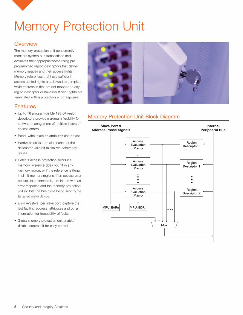
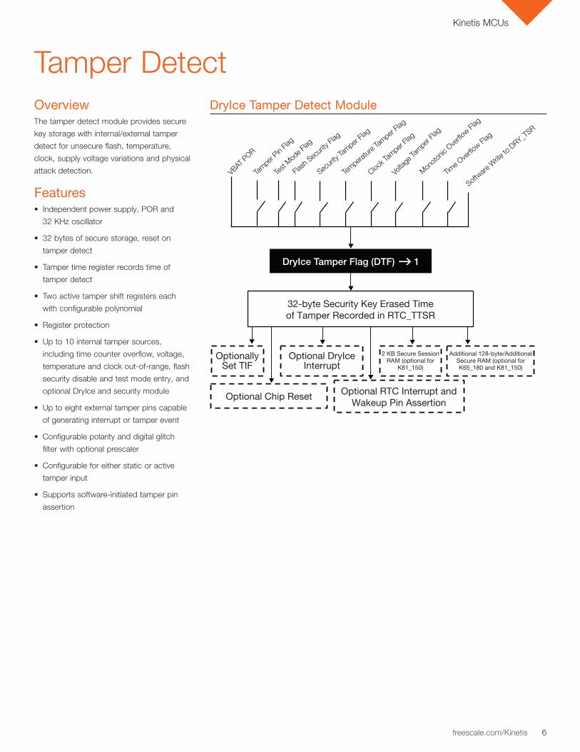
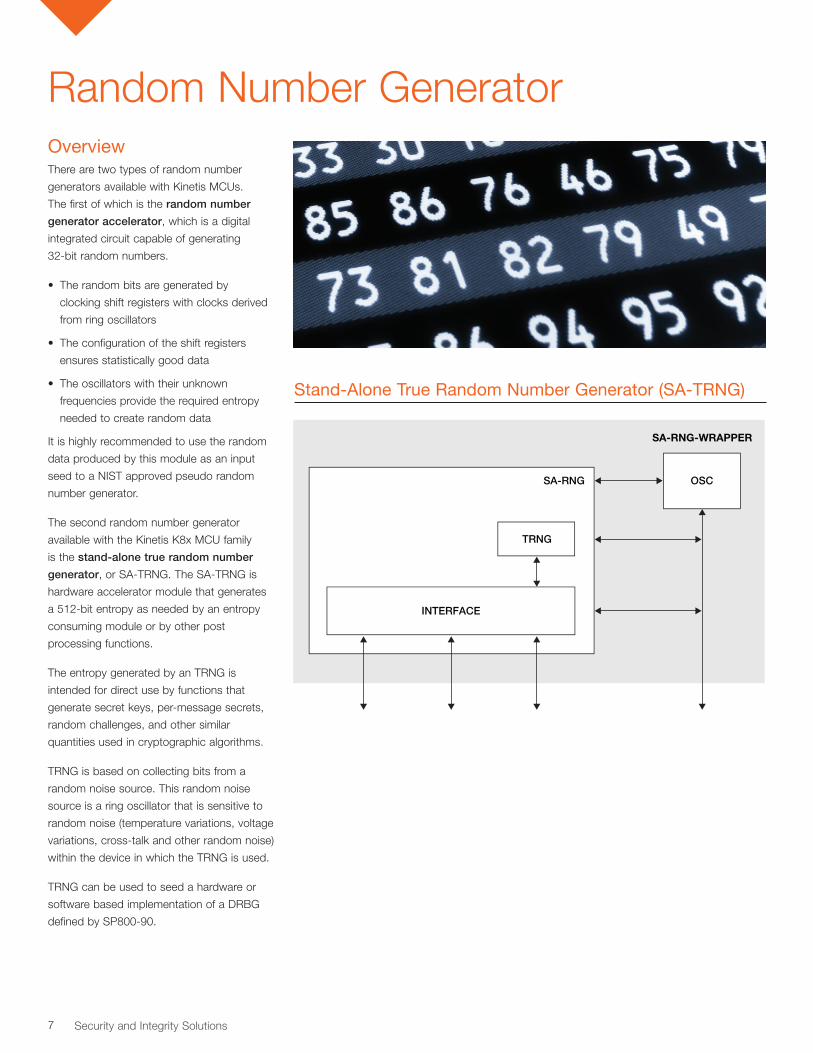
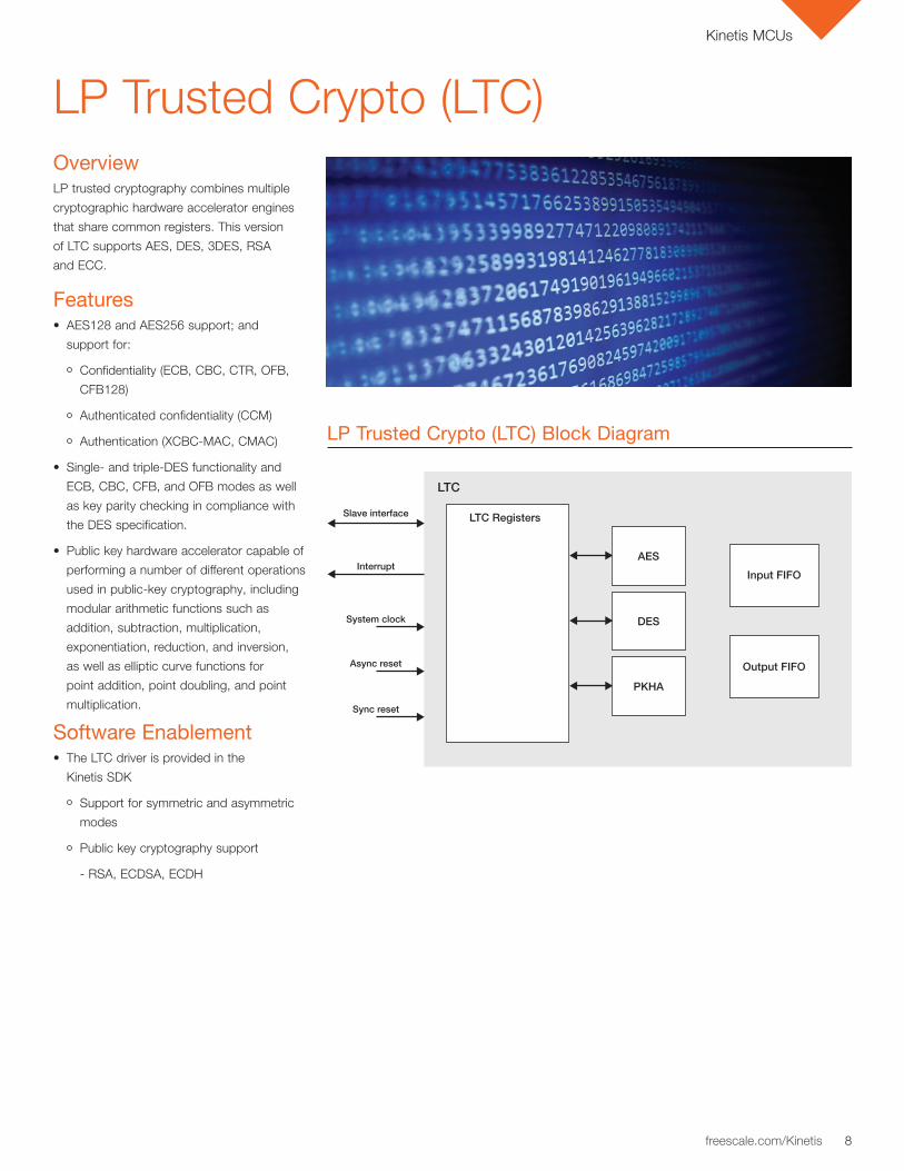
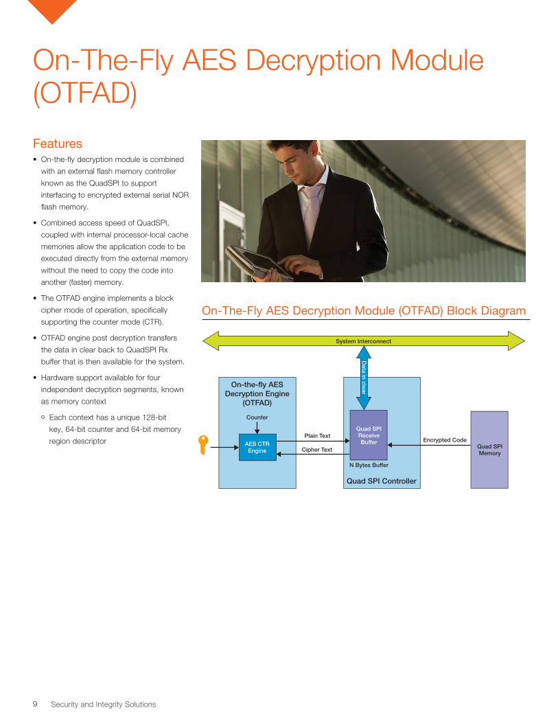