Embed Size (px)
Citation preview

• Op Amps• 741, 356• Imperfections• Op‐amp applications
6.101 Spring 2017 Lecture 7 1
Acknowledgements: Ron Roscoe,Neamen, Donald: Microelectronics Circuit Analysis and Design, 3rd Edition
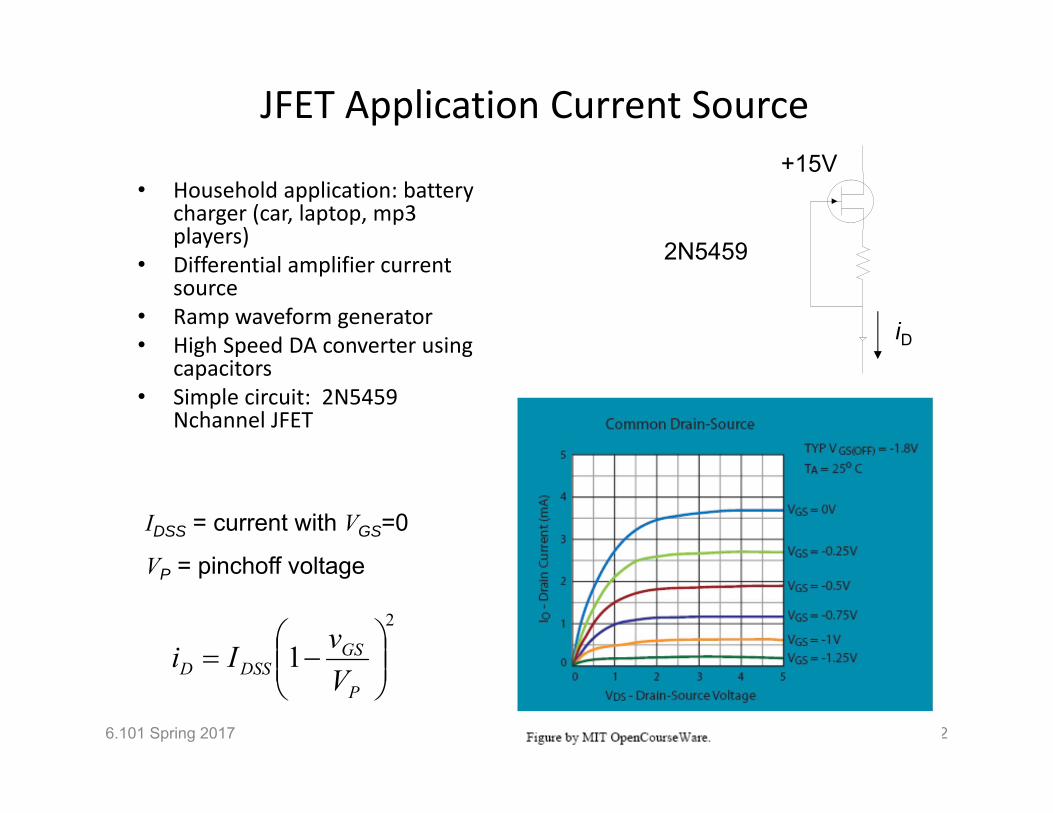
JFET Application Current Source
• Household application: battery charger (car, laptop, mp3 players)
• Differential amplifier current source
• Ramp waveform generator• High Speed DA converter using
capacitors• Simple circuit: 2N5459
Nchannel JFET
2
1
P
GSDSSD V
vIi
6.101 Spring 2017 2
+15V
2N5459
IDSS = current with VGS=0
VP = pinchoff voltage
iD
6.101 Spring 2017 3
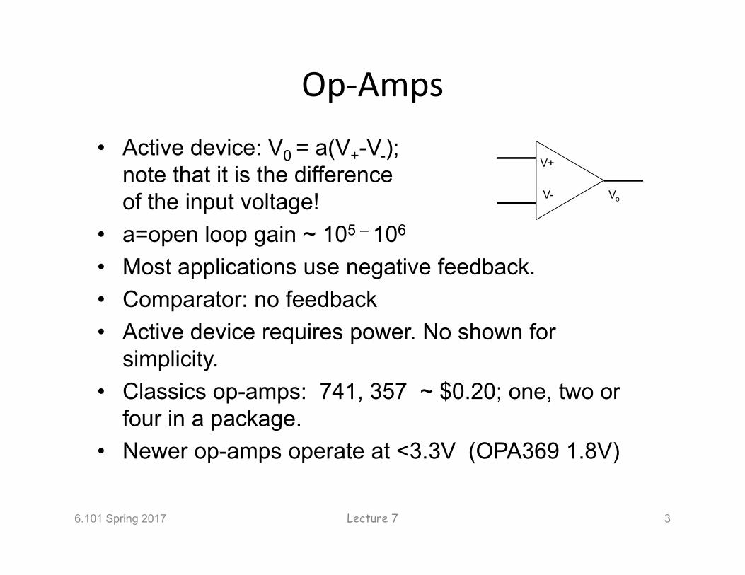
Op‐Amps
• Active device: V0 = a(V+-V-); note that it is the difference of the input voltage!
• a=open loop gain ~ 105 – 106
• Most applications use negative feedback.• Comparator: no feedback• Active device requires power. No shown for
simplicity.• Classics op-amps: 741, 357 ~ $0.20; one, two or
four in a package. • Newer op-amps operate at <3.3V (OPA369 1.8V)
V+
VoV-
Lecture 7
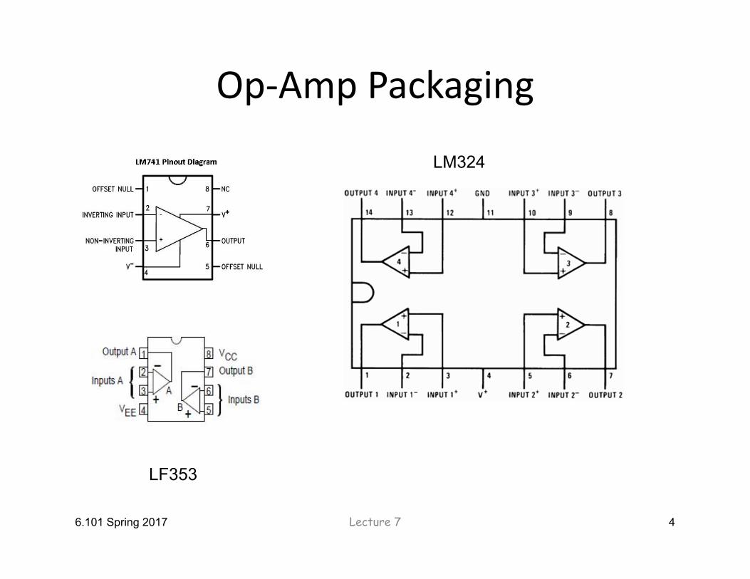
Op‐Amp Packaging
6.101 Spring 2017 4
LM324
LF353
Lecture 7
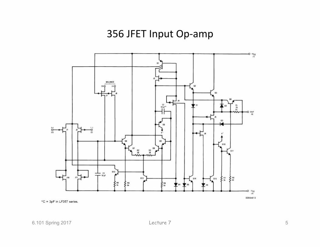
356 JFET Input Op‐amp
6.101 Spring 2017 5Lecture 7
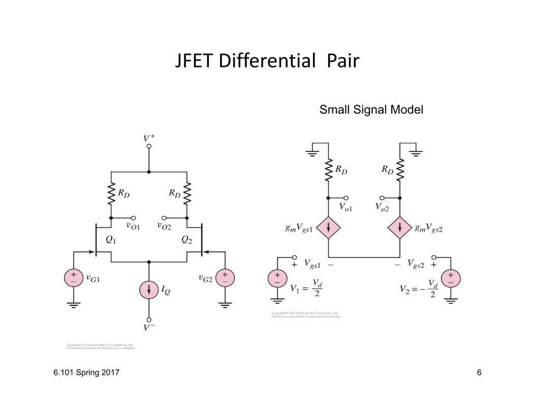
JFET Differential Pair
6.101 Spring 2017 6
Small Signal Model
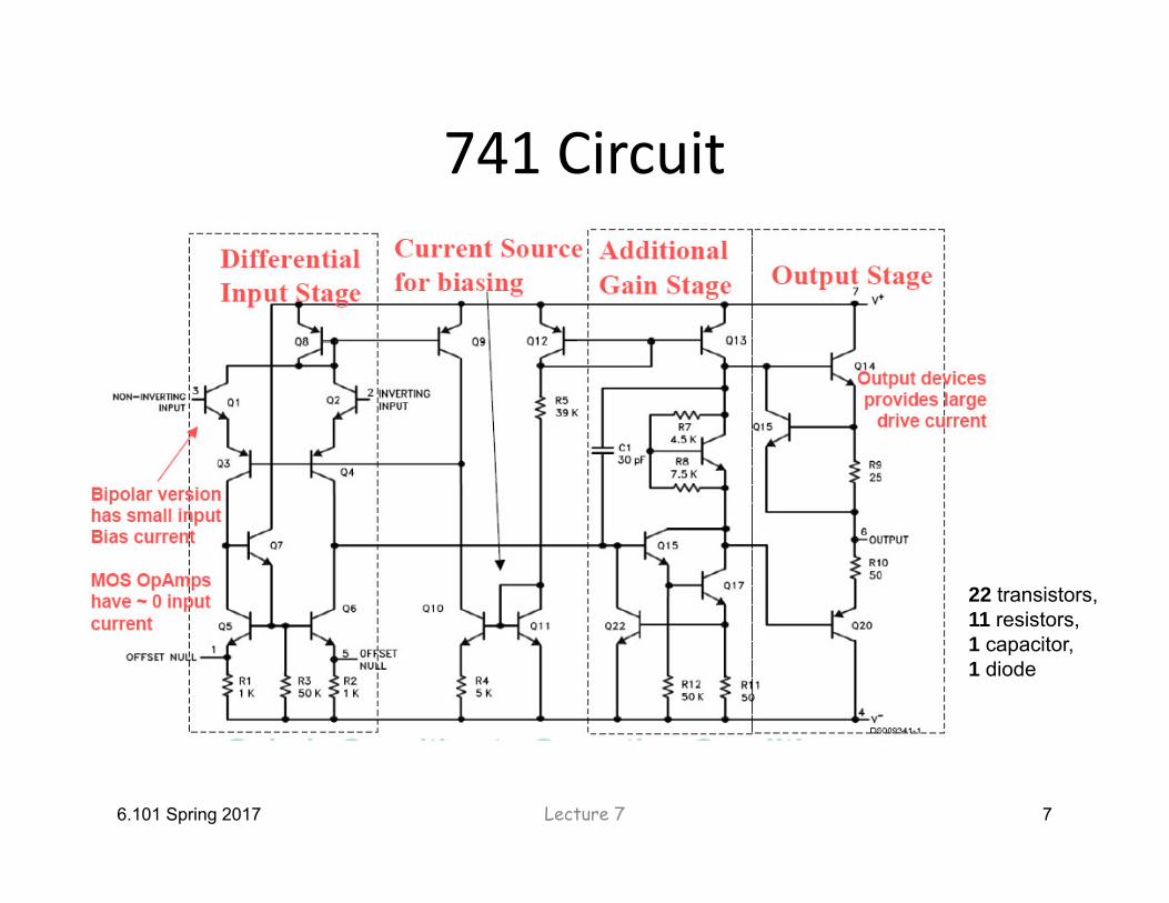
741 Circuit
6.101 Spring 2017 7
22 transistors, 11 resistors, 1 capacitor, 1 diode
Lecture 7
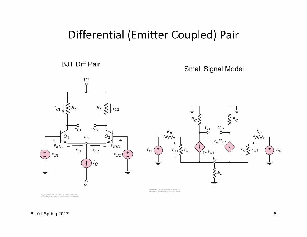
Differential (Emitter Coupled) Pair
6.101 Spring 2017 8
BJT Diff PairSmall Signal Model
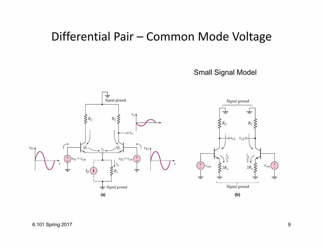
Differential Pair – Common Mode Voltage
6.101 Spring 2017 9
Small Signal Model
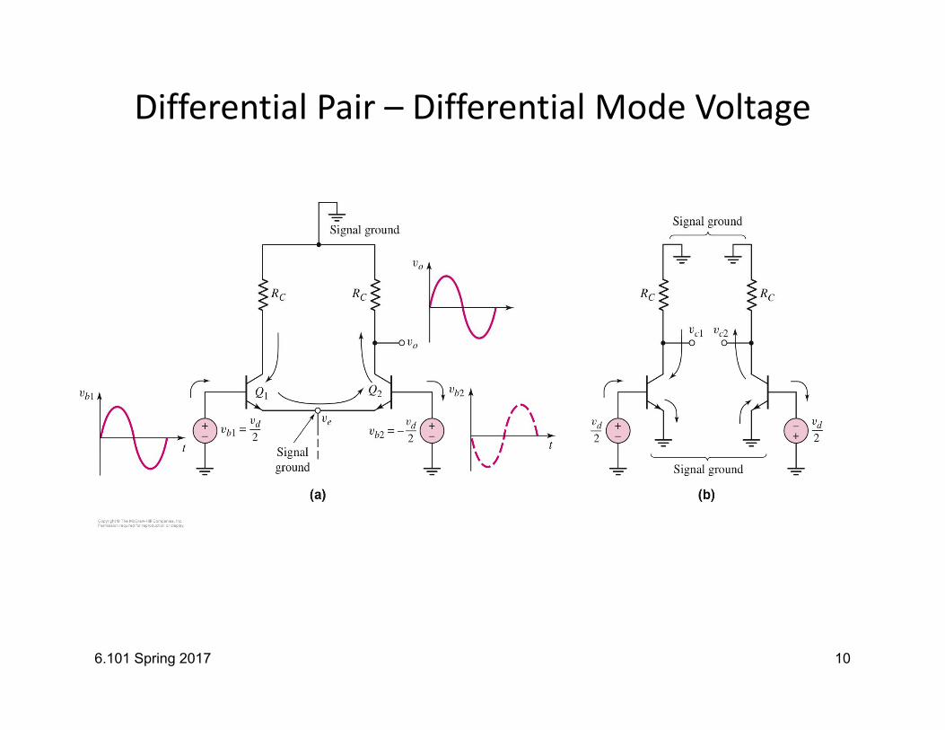
Differential Pair – Differential Mode Voltage
6.101 Spring 2017 10
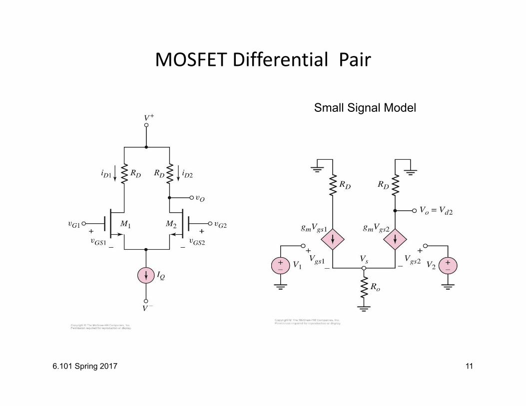
MOSFET Differential Pair
6.101 Spring 2017 11
Small Signal Model
+
6.101 Spring 2017 12
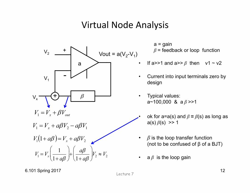
Virtual Node Analysis
V1
V2 Vout = a(V2-V1)
Vx
-
+
a • If a>>1 and a>> β then v1 ~ v2
• Current into input terminals zero by design
• Typical values: a~100,000 & a β >>1
• ok for a=a(s) and β = β(s) as long as a(s) β(s) >> 1
• β is the loop transfer function(not to be confused of β of a BJT)
• a β is the loop gain
outx VVV 1
121 VaVaVV x
21 1 VaVaV x
V1 Vx1
1 a
a1 a
V2 V2
a = gainβ = feedback or loop function
Lecture 7
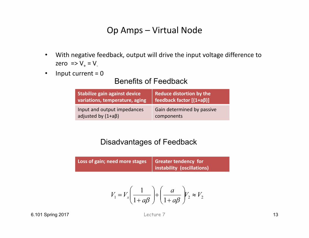
Op Amps – Virtual Node
• With negative feedback, output will drive the input voltage difference to zero => V+ = V‐
• Input current = 0
6.101 Spring 2017 13
Benefits of FeedbackStabilize gain against device variations, temperature, aging
Reduce distortion by the feedback factor [(1+aβ)]
Input and output impedances adjusted by (1+aβ)
Gain determined by passive components
Disadvantages of Feedback
Loss of gain; need more stages Greater tendency for instability (oscillations)
Lecture 7
221 111 VV
aa
aVV x
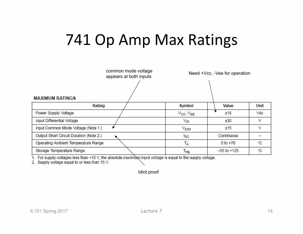
741 Op Amp Max Ratings
6.101 Spring 2017 14
Need +Vcc, -Vee for operationcommon mode voltage appears at both inputs
Idiot proof
Lecture 7
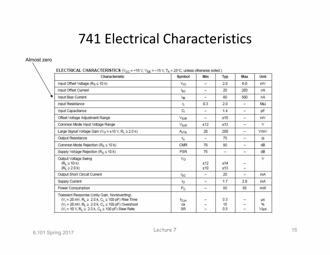
741 Electrical Characteristics
6.101 Spring 2017 15
Almost zero
Lecture 7
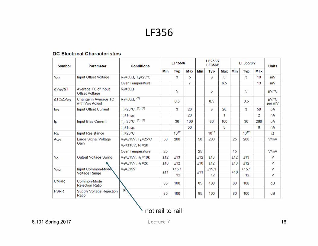
LF356
6.101 Spring 2017 16Lecture 7
not rail to rail
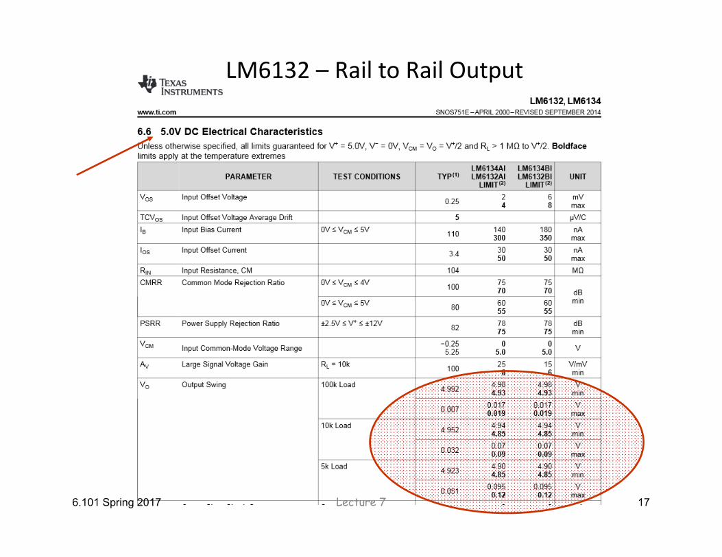
LM6132 – Rail to Rail Output
6.101 Spring 2017 17Lecture 7
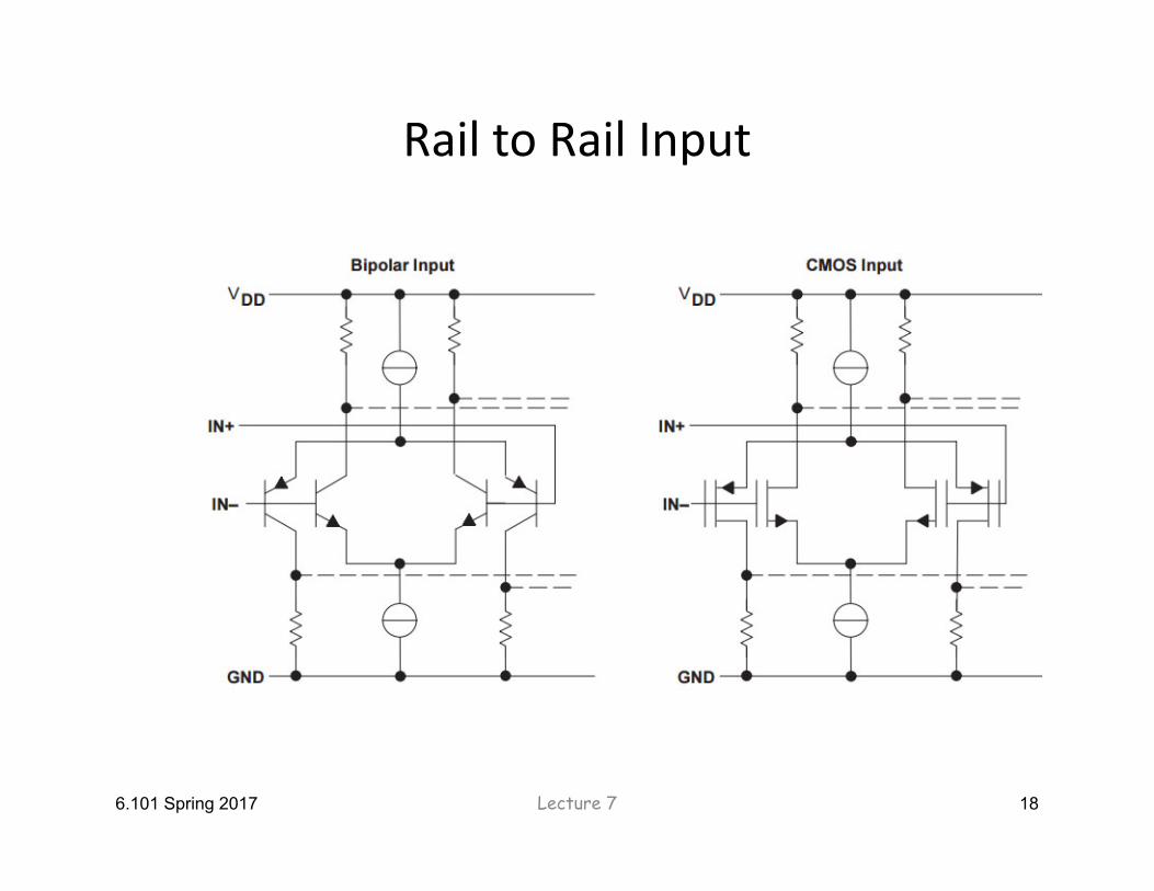
Rail to Rail Input
6.101 Spring 2017 18Lecture 7
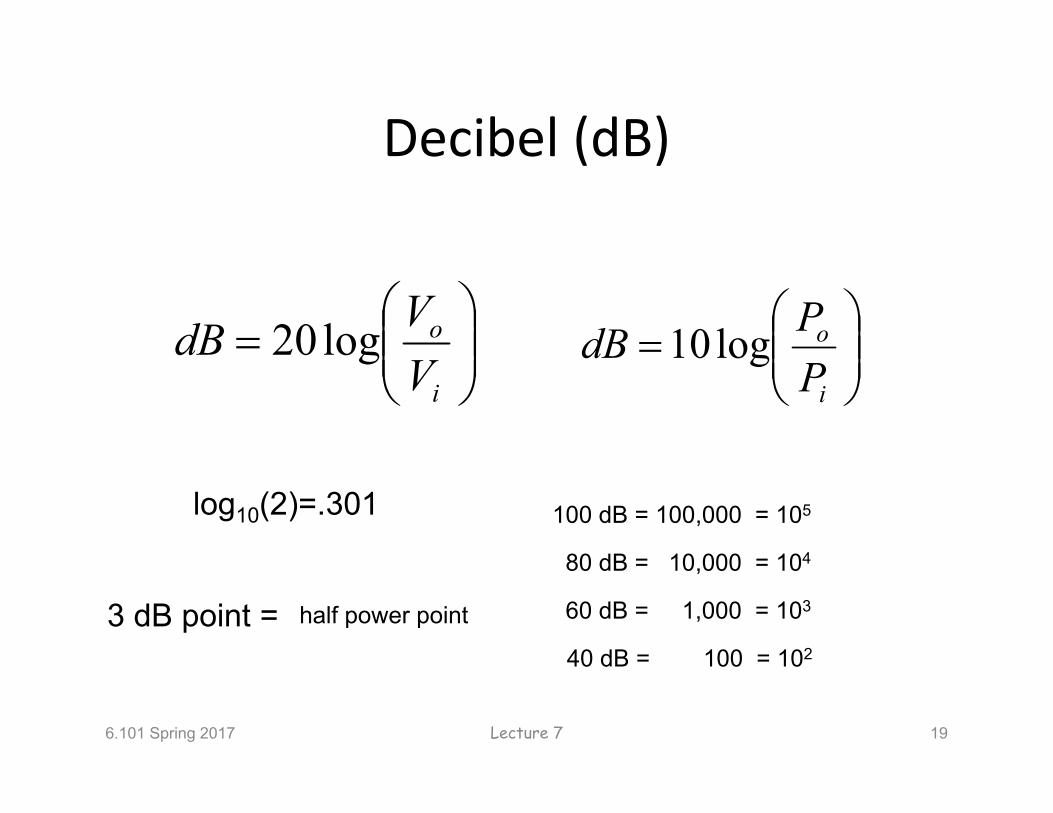
Decibel (dB)
i
o
VVdB log20
i
o
PPdB log10
6.101 Spring 2017 19
3 dB point =
log10(2)=.301 100 dB = 100,000 = 105
Lecture 7
80 dB = 10,000 = 104
60 dB = 1,000 = 103
40 dB = 100 = 102
half power point
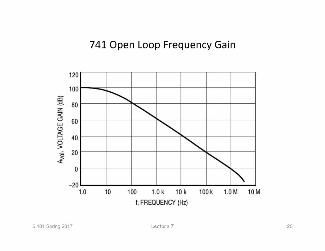
741 Open Loop Frequency Gain
6.101 Spring 2017 20Lecture 7
Non‐Inverting Amplifer
6.101 Spring 2017 21
-
++15
A
2
3
4
76
vin+
vout
_
+
_ -15
Rs
R2
R1
v+
v-
1
2
1
21
;21
1
21
1
1
;
RRAor
RRR
vv
vRR
Rvso
vvbutvRR
Rv
vvthereforecurrentinputZero
v
in
out
outin
out
in
AAA
vv
RRR
vin
out
1
21
1
for finite A
β (not to be confused with βof a BJT)
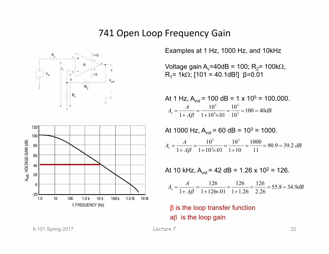
741 Open Loop Frequency Gain
6.101 Spring 2017 22
Examples at 1 Hz, 1000 Hz, and 10kHz
Voltage gain Av=40dB = 100; R2= 100k, R1= 1k; [101 = 40.1dB!] β=0.01
At 1 Hz, Avol = 100 dB = 1 x 105 = 100,000.
At 1000 Hz, Avol = 60 dB = 103 = 1000.
At 10 kHz, Avol = 42 dB = 1.26 x 102 = 126.
-
++15
A
2
3
4
76
vin+
vout
_
+
_ -15
Rs
R2
R1
v+
v-
dBA
AAv 401001010
01.10110
1 3
5
5
5
dBAAAv 2.399.90
111000
10110
01.10110
1
3
3
3
dBA
AAv 9.348.5526.2
12626.11
12601.1261
1261
β is the loop transfer functionaβ is the loop gain
Lecture 7
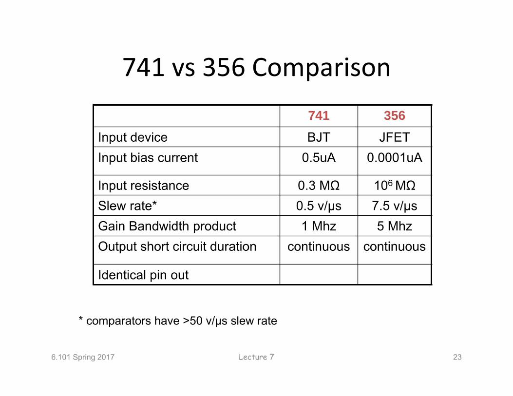
741 vs 356 Comparison741 356
Input device BJT JFETInput bias current 0.5uA 0.0001uA
Input resistance 0.3 MΩ 106 MΩSlew rate* 0.5 v/μs 7.5 v/μsGain Bandwidth product 1 Mhz 5 MhzOutput short circuit duration continuous continuous
Identical pin out
6.101 Spring 2017 23
* comparators have >50 v/μs slew rate
Lecture 7
So Why BJT in Op‐amps?
6.101 Spring 2017 24
BJTs have higher transconductance (gain), better consistency in spec between pieces, and in some applications, lower noise than FETs.
Like most JFET op amps, the LF356 has a relatively high offset voltage, and relatively high drifts. BJT op-amps tend to have much lower offset voltage and drifts.
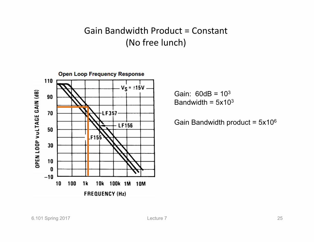
Gain Bandwidth Product = Constant(No free lunch)
6.101 Spring 2017 Lecture 7 25
Gain: 60dB = 103
Bandwidth = 5x10³
Gain Bandwidth product = 5x10⁶
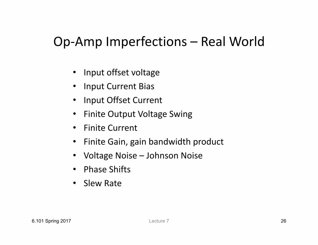
Op‐Amp Imperfections – Real World
• Input offset voltage• Input Current Bias• Input Offset Current• Finite Output Voltage Swing• Finite Current• Finite Gain, gain bandwidth product• Voltage Noise – Johnson Noise• Phase Shifts• Slew Rate
6.101 Spring 2017 26Lecture 7
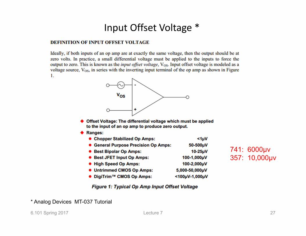
Input Offset Voltage *
6.101 Spring 2017 Lecture 7 27
* Analog Devices MT-037 Tutorial
741: 6000μv357: 10,000μv
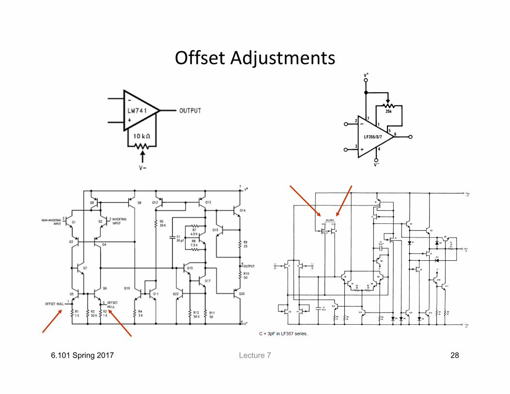
Offset Adjustments
6.101 Spring 2017 28Lecture 7
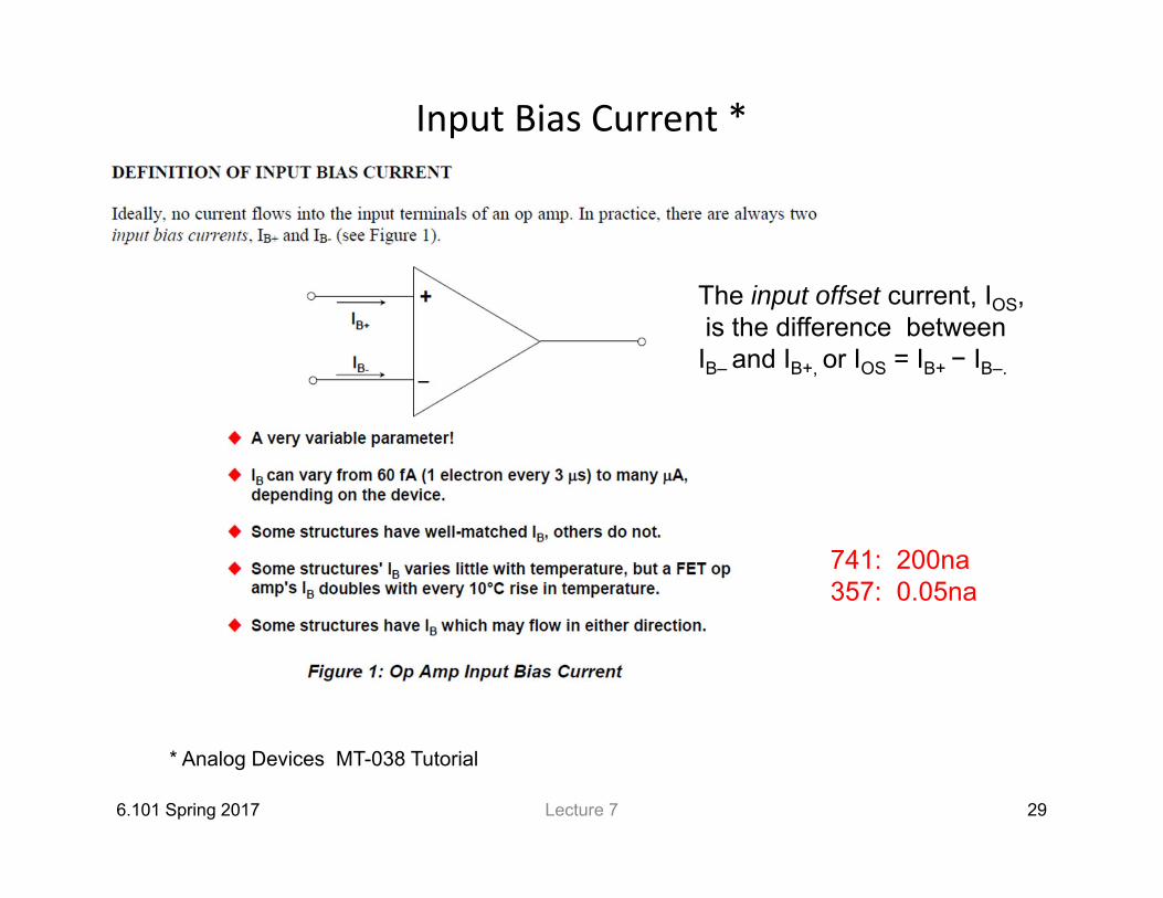
Input Bias Current *
6.101 Spring 2017 29Lecture 7
The input offset current, IOS,is the difference between IB– and IB+, or IOS = IB+ − IB–.
* Analog Devices MT-038 Tutorial
741: 200na357: 0.05na
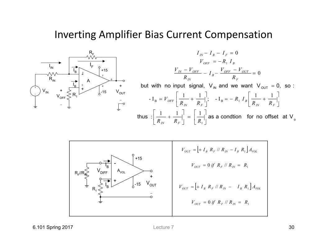
Inverting Amplifier Bias Current Compensation
6.101 Spring 2017 30Lecture 7
-
+
+15
A
2
3 4
76
VIN
+VOUT
_
+
_ -15
RIN
RF
IIN IFIB
R1
IB+
VOFF
_
o
OUTIN
Vat offset no for condtion aas thus
:so 0, V want weand Vsignal, input no withbut
1
1BB
1
1 11 :
11I-;11I-
0
0
RRR
RRIR
RRV
RVVI
RVV
IRVIII
FIN
FINB
FINOFF
F
OUTOFFB
IN
OFFIN
BOFF
FBIN
-
+
+15
AVOLVDIFF
-15
RF//RIN
R1
IB
IB
+VOUT
_
1
1
// 0
//
RRRifV
ARIRRIV
INFOUT
VOLBINFBOUT
1
1
// 0
//
RRRifV
ARIRRIV
INFOUT
VOLBINFBOUT
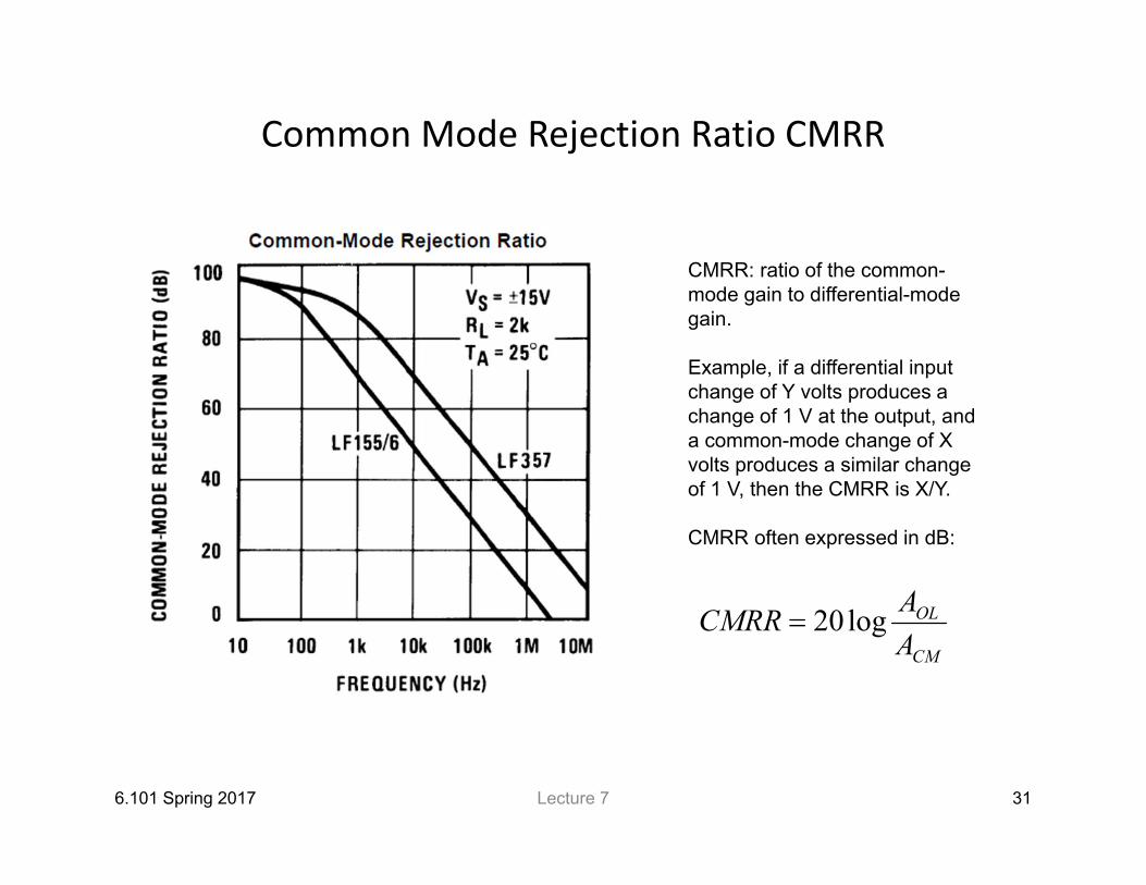
Common Mode Rejection Ratio CMRR
6.101 Spring 2017 31Lecture 7
CMRR: ratio of the common-mode gain to differential-mode gain.
Example, if a differential input change of Y volts produces a change of 1 V at the output, and a common-mode change of X volts produces a similar change of 1 V, then the CMRR is X/Y.
CMRR often expressed in dB:
CM
OL
AACMRR log20
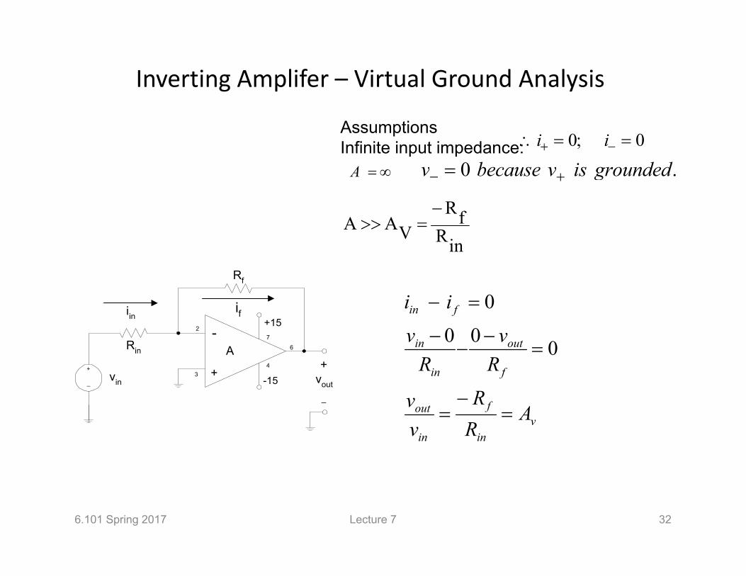
Inverting Amplifer – Virtual Ground Analysis
6.101 Spring 2017 Lecture 7 32
AssumptionsInfinite input impedance:
-
+
+15
A
2
34
7
6
vin
+vout
_
+
_ -15
Rin
Rf
iin if
vin
f
in
out
f
out
in
in
fin
ARR
vv
Rv
Rv
ii
000
0
i i0 0;
A v because v is grounded 0 .
inRfR
VAA
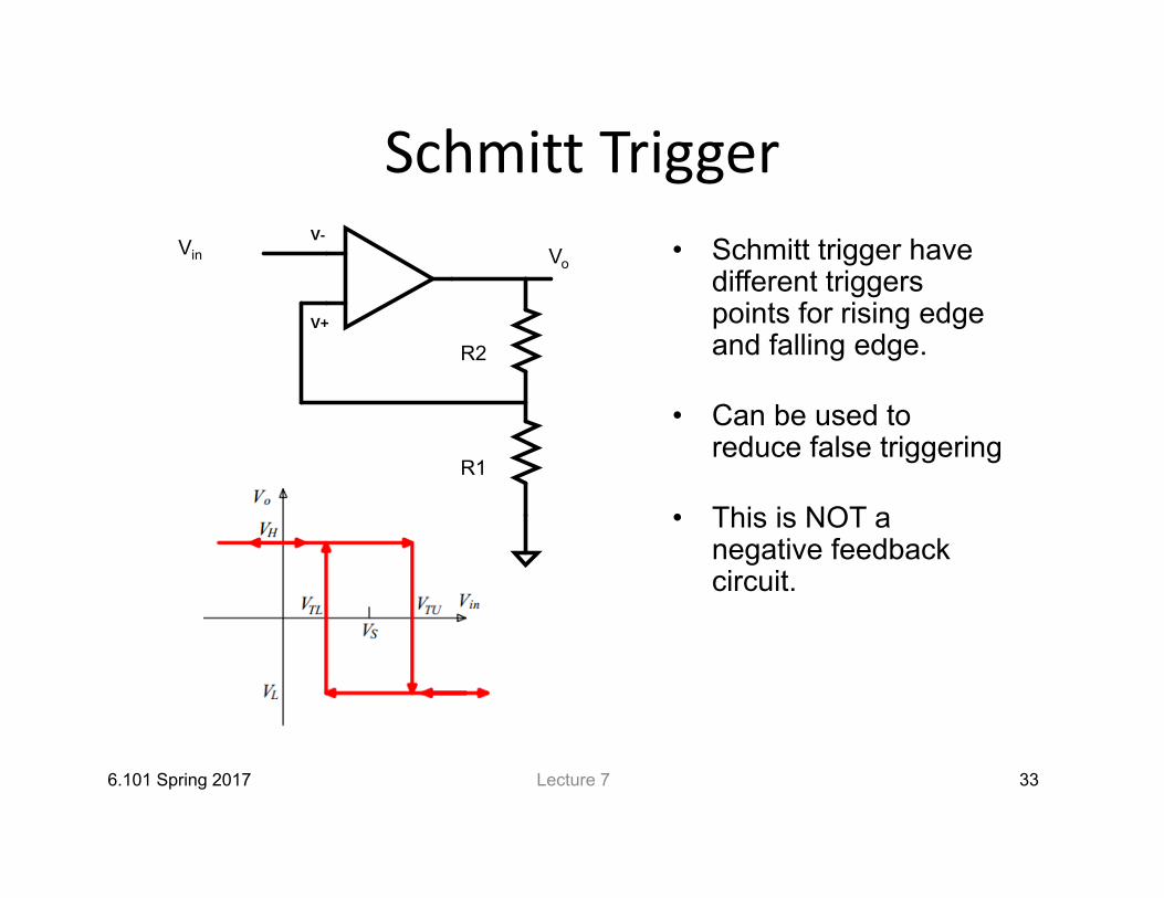
Schmitt Trigger• Schmitt trigger have
different triggers points for rising edge and falling edge.
• Can be used to reduce false triggering
• This is NOT a negative feedback circuit.
Vin Vo
V-
V+
R1
R2
6.101 Spring 2017 33Lecture 7
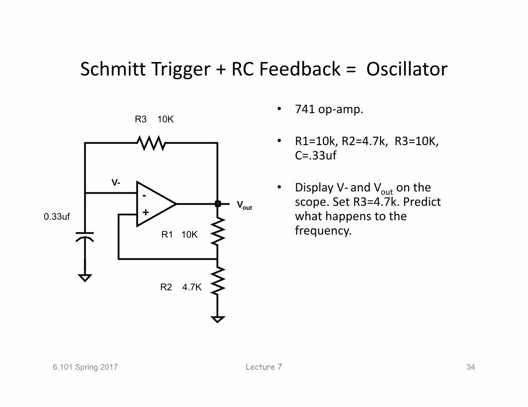
Schmitt Trigger + RC Feedback = Oscillator
• 741 op‐amp.
• R1=10k, R2=4.7k, R3=10K, C=.33uf
• Display V‐ and Vout on the scope. Set R3=4.7k. Predict what happens to the frequency.
6.101 Spring 2017 34
-+
R3 10K
R1 10K
R2 4.7K
0.33uf
V-
Vout
Lecture 7
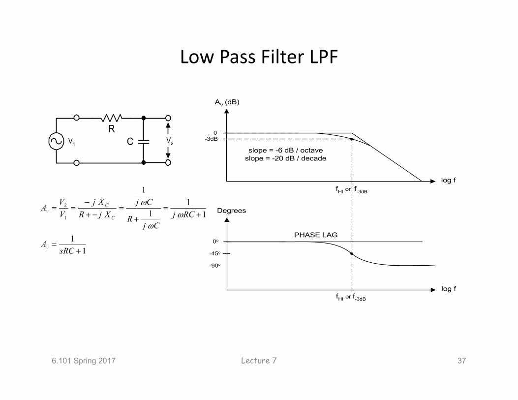
High Pass Filter HPF
6.101 Spring 2017 35
RV1 V2
C
1CRsCRs
1CRjCRj
Cj1R
RVVA
1
2v
log f
AV (dB)
-3dB
fLO or f-3dB
slope = 6 dB / octaveslope = 20 dB / decade
0
log f
Degrees
45o
fLO or f-3dB
90o
0o
-45o
PHASE LEAD
Lecture 7
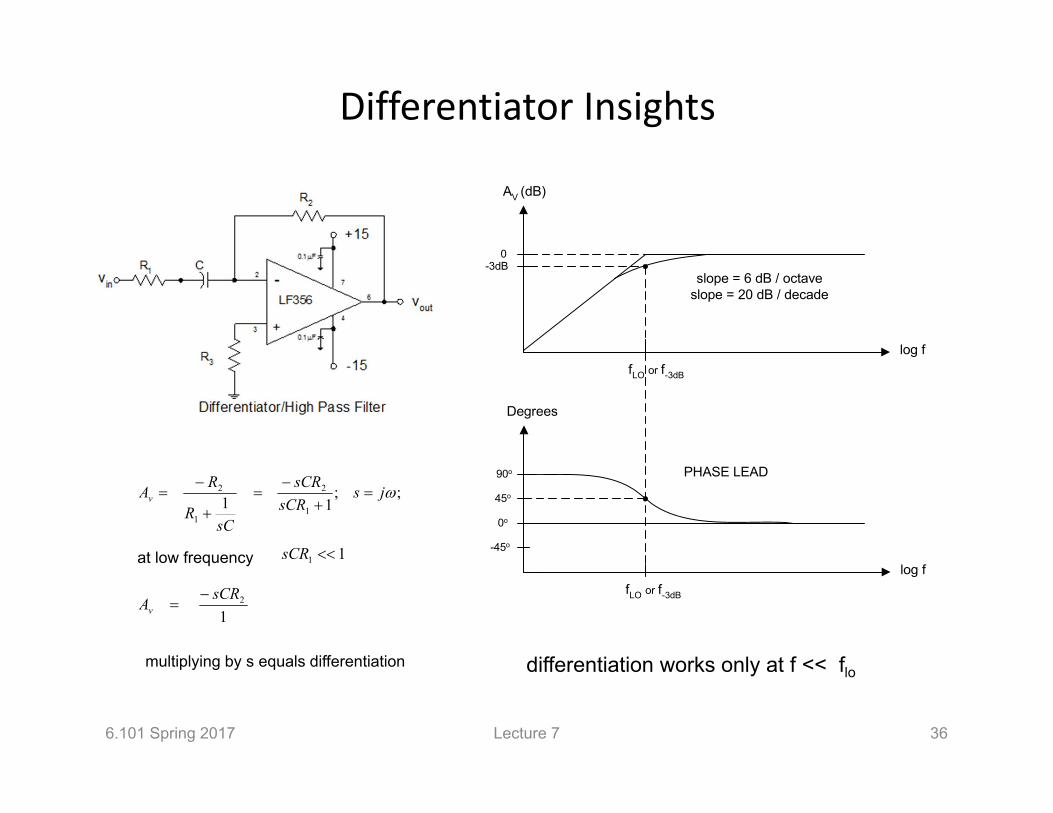
Differentiator Insights
6.101 Spring 2017 Lecture 7 36
;;11 1
2
1
2 jssCR
sCR
sCR
RAv
at low frequency 11 sCR
12sCRAv
multiplying by s equals differentiation
log f
AV (dB)
-3dB
fLO or f-3dB
slope = 6 dB / octaveslope = 20 dB / decade
0
log f
Degrees
45o
fLO or f-3dB
90o
0o
-45o
PHASE LEAD
differentiation works only at f << flo
Low Pass Filter LPF
6.101 Spring 2017 37
RV1 V2C
11
11
1
1
1
2
sRCA
RCjCj
R
CjXjR
XjVVA
v
C
Cv
log f
AV (dB)
-3dB
fHI or f-3dB
slope = -6 dB / octaveslope = -20 dB / decade
0
log f
Degrees
-45o
fHI or f-3dB
0o
-90o
PHASE LAG
Lecture 7
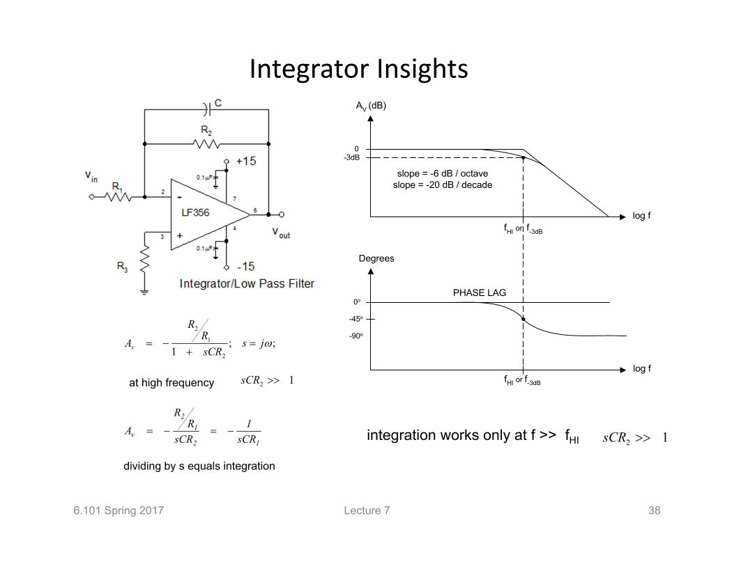
Integrator Insights
6.101 Spring 2017 Lecture 7 38
;;1 2
1
2
jssCRR
R
Av
12 sCR
12
12
v sCR1
sCRR
R
A
at high frequency
dividing by s equals integration
log f
AV (dB)
-3dB
fHI or f-3dB
slope = -6 dB / octaveslope = -20 dB / decade
0
log f
Degrees
-45o
fHI or f-3dB
0o
-90o
PHASE LAG
integration works only at f >> fHI 12 sCR
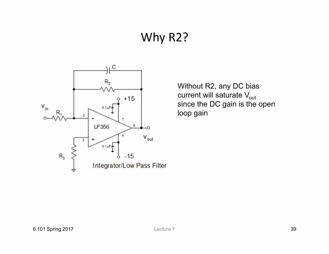
Why R2?
6.101 Spring 2017 39
Without R2, any DC bias current will saturate Vout since the DC gain is the open loop gain
Lecture 7
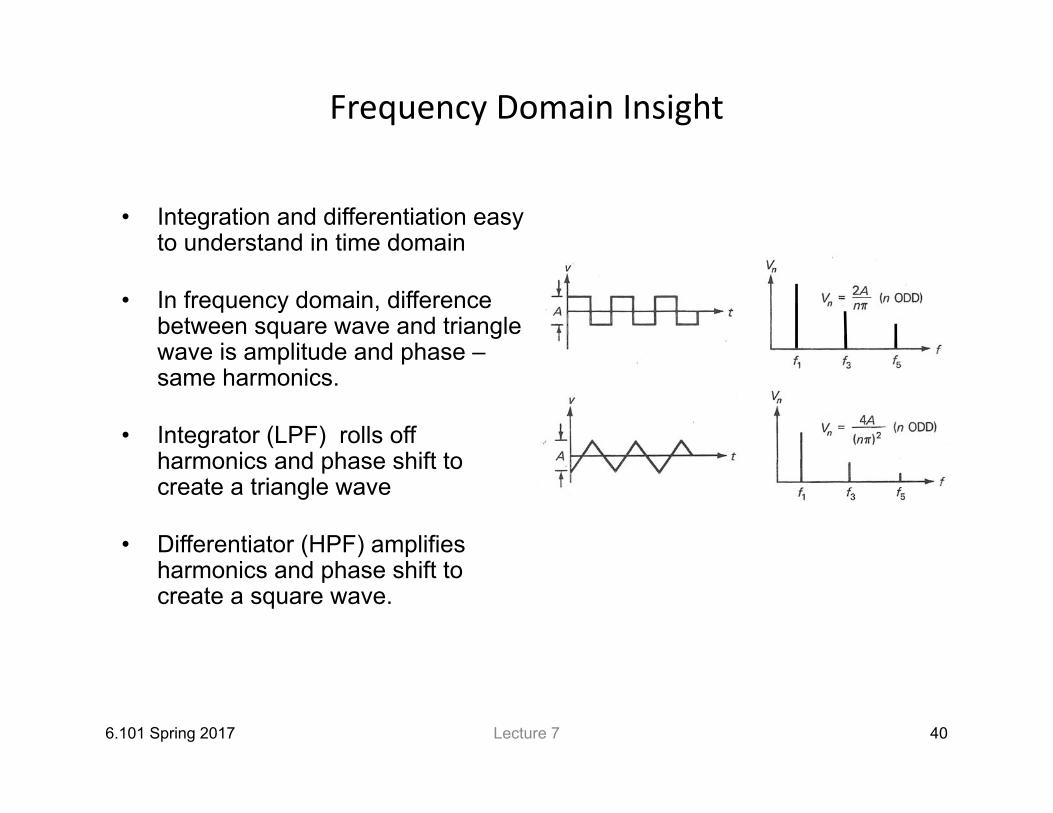
Frequency Domain Insight
6.101 Spring 2017 40Lecture 7
• Integration and differentiation easy to understand in time domain
• In frequency domain, difference between square wave and triangle wave is amplitude and phase –same harmonics.
• Integrator (LPF) rolls off harmonics and phase shift to create a triangle wave
• Differentiator (HPF) amplifies harmonics and phase shift to create a square wave.
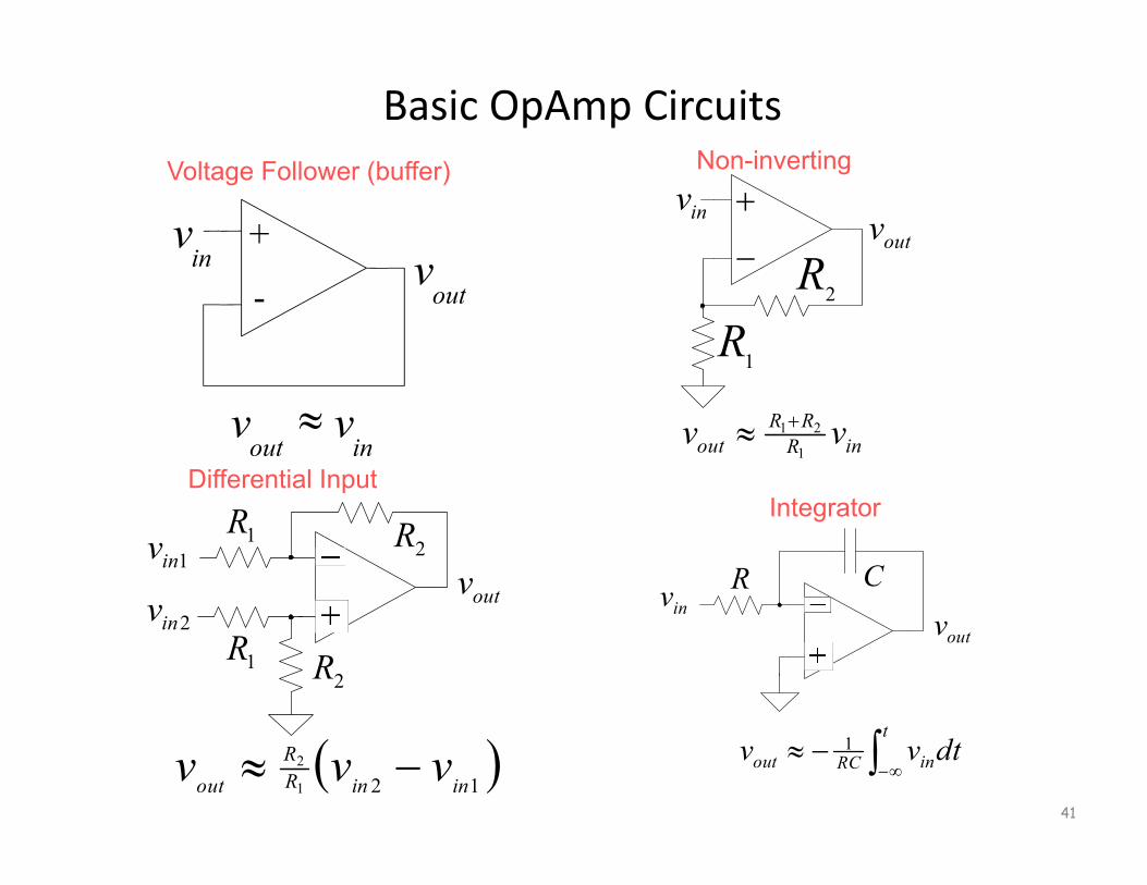
Basic OpAmp CircuitsVoltage Follower (buffer)
invoutv
2R
1R
inRRR
out vv1
21
Non-inverting
inv
outv
1invoutv
2inv
1R
1R
2R
2R
121
2
ininRR
out vvv
Differential Inputinout
vv
invoutv
R C
t
inRCout dtvv 1
Integrator
+
-
41
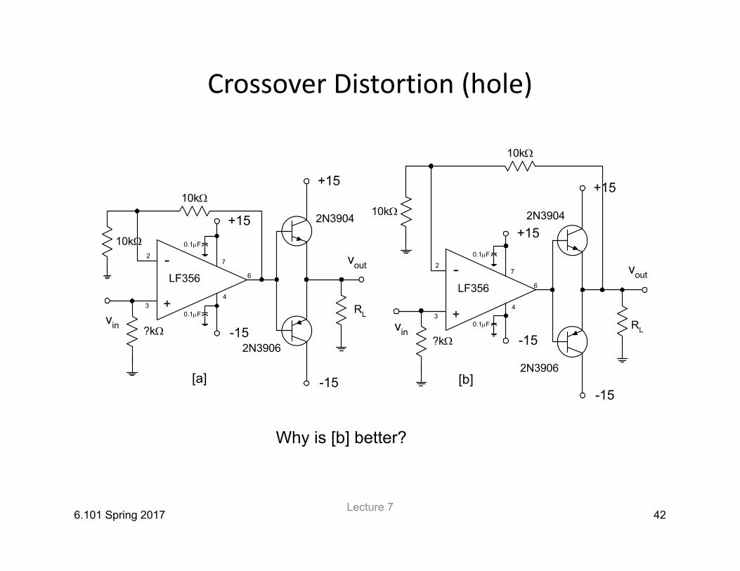
Crossover Distortion (hole)
6.101 Spring 2017 42Lecture 7
[a]
vout-
+
LF356
2
34
7
6
vin
RL
2N3904
2N3906
[b]
-
+
LF356
2
34
7
6
vin
2N3904
2N3906
vout
RL
0.1F
0.1F
+15
-150.1F
+15
-15
0.1F
+15
-15-15
+1510k
10k
10k
10k
?k?k
Why is [b] better?
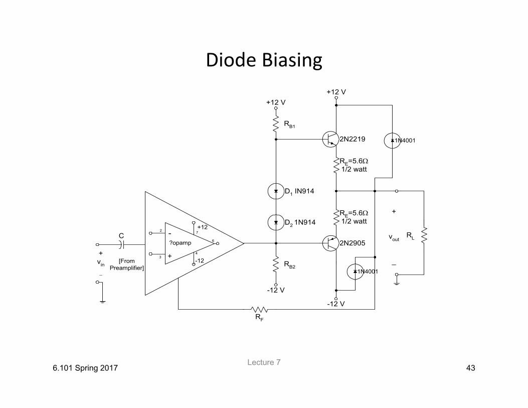
Diode Biasing
6.101 Spring 2017 43
C
+vin
_
RF
2N2219
2N2905
D2 1N914
D1 IN914
RE=5.61/2 watt
RB1
+12 V
RL
-12 V
+12 V
+
vout
_RB2
-12 V
RE=5.61/2 watt
+122
34
7
6
-12
-
+
?opamp
[FromPreamplifier]
1N4001
1N4001
Lecture 7