Embed Size (px)
Citation preview
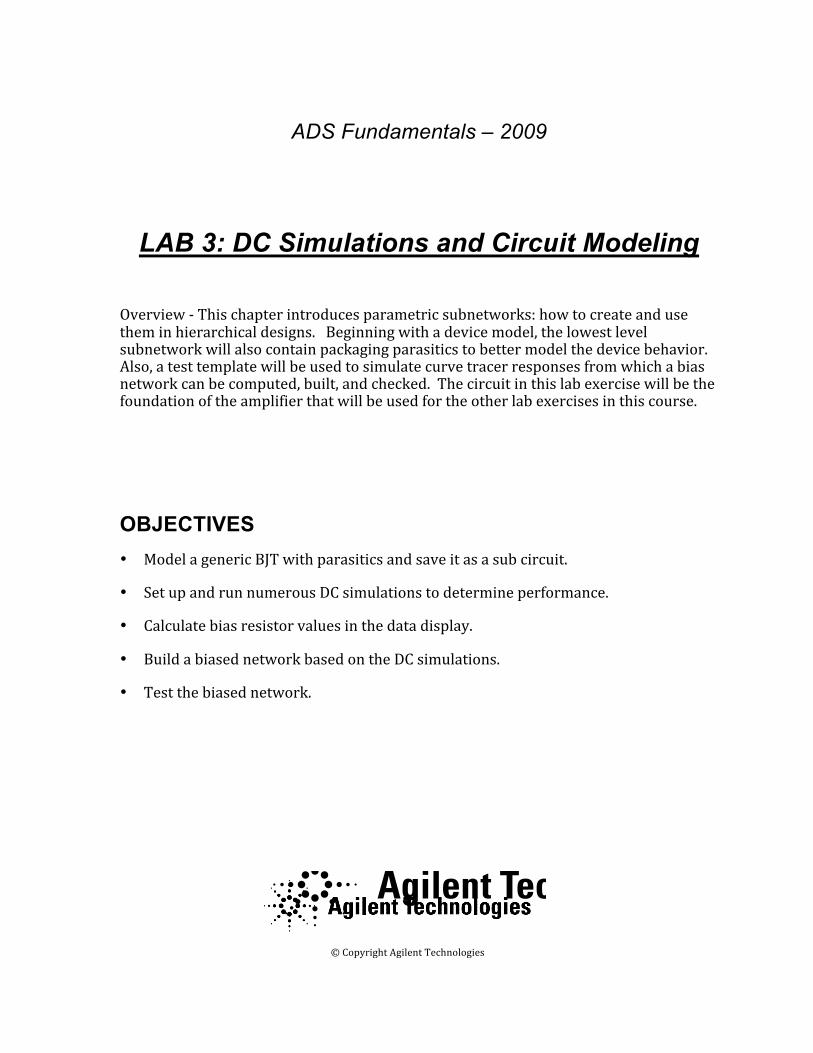
ADS Fundamentals – 2009
LAB 3: DC Simulations and Circuit Modeling
Overview‐Thischapterintroducesparametricsubnetworks:howtocreateandusetheminhierarchicaldesigns.Beginningwithadevicemodel,thelowestlevelsubnetworkwillalsocontainpackagingparasiticstobettermodelthedevicebehavior.Also,atesttemplatewillbeusedtosimulatecurvetracerresponsesfromwhichabiasnetworkcanbecomputed,built,andchecked.Thecircuitinthislabexercisewillbethefoundationoftheamplifierthatwillbeusedfortheotherlabexercisesinthiscourse.
OBJECTIVES • ModelagenericBJTwithparasiticsandsaveitasasubcircuit.
• SetupandrunnumerousDCsimulationstodetermineperformance.
• Calculatebiasresistorvaluesinthedatadisplay.
• BuildabiasednetworkbasedontheDCsimulations.
• Testthebiasednetwork.
©CopyrightAgilentTechnologies2009
Lab 3: DC Simulations
3‐2 ©CopyrightAgilentTechnologies2009
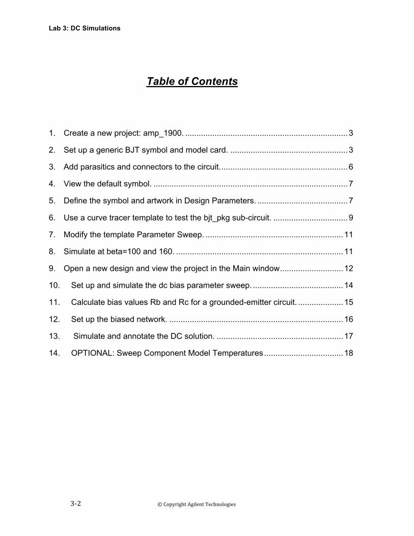
Table of Contents
1. Create a new project: amp_1900. ........................................................................3
2. Set up a generic BJT symbol and model card. ....................................................3
3. Add parasitics and connectors to the circuit.........................................................6
4. View the default symbol. ......................................................................................7
5. Define the symbol and artwork in Design Parameters. ........................................7
6. Use a curve tracer template to test the bjt_pkg sub-circuit. .................................9
7. Modify the template Parameter Sweep. .............................................................11
8. Simulate at beta=100 and 160. ..........................................................................11
9. Open a new design and view the project in the Main window............................12
10. Set up and simulate the dc bias parameter sweep. ........................................14
11. Calculate bias values Rb and Rc for a grounded-emitter circuit. ....................15
12. Set up the biased network. .............................................................................16
13. Simulate and annotate the DC solution. ........................................................17
14. OPTIONAL: Sweep Component Model Temperatures ...................................18
Lab 3: DC Simulations
33‐3©CopyrightAgilentTechnologies
2009
PROCEDUREThecircuityoubuildforthislabexercisewillbeusedasthelowerlevelsub‐circuitforalloftheamplifierlabstofollow.1. Createanewproject:amp_1900.
a. Ifyouhavenotalreadycreatedthisproject,doitnow.Then,inthisnewproject,amp_1900,openanewschematicwindowandsaveitwiththename:bjt_pkg.Also,setanydesiredOptions>Preferences.
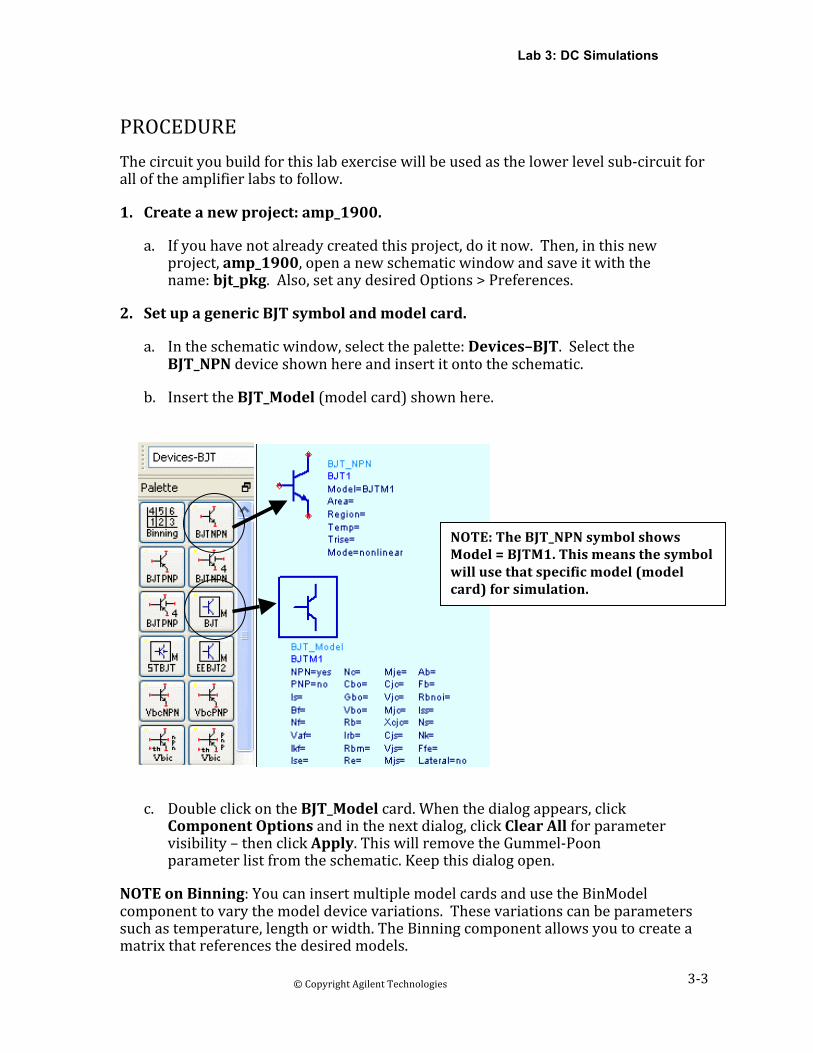
2. SetupagenericBJTsymbolandmodelcard.
a. Intheschematicwindow,selectthepalette:Devices–BJT.SelecttheBJT_NPNdeviceshownhereandinsertitontotheschematic.
b. InserttheBJT_Model(modelcard)shownhere.
c. DoubleclickontheBJT_Modelcard.Whenthedialogappears,clickComponentOptionsandinthenextdialog,clickClearAllforparametervisibility–thenclickApply.ThiswillremovetheGummel‐Poonparameterlistfromtheschematic.Keepthisdialogopen.
NOTEonBinning:YoucaninsertmultiplemodelcardsandusetheBinModelcomponenttovarythemodeldevicevariations.Thesevariationscanbeparameterssuchastemperature,lengthorwidth.TheBinningcomponentallowsyoutocreateamatrixthatreferencesthedesiredmodels.
NOTE:TheBJT_NPNsymbolshowsModel=BJTM1.Thismeansthesymbolwillusethatspecificmodel(modelcard)forsimulation.
Lab 3: DC Simulations
3‐4 ©CopyrightAgilentTechnologies2009
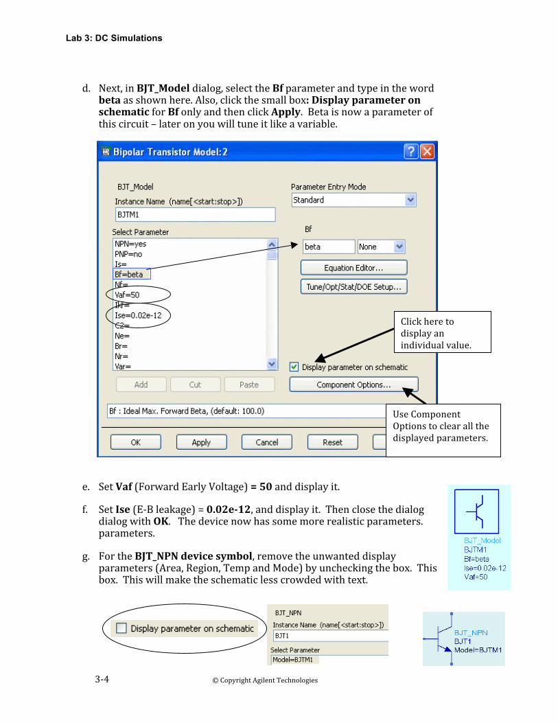
d. Next,inBJT_Modeldialog,selecttheBfparameterandtypeinthewordbetaasshownhere.Also,clickthesmallbox:DisplayparameteronschematicforBfonlyandthenclickApply.Betaisnowaparameterofthiscircuit–lateronyouwilltuneitlikeavariable.
e. SetVaf(ForwardEarlyVoltage)=50anddisplayit.
f. SetIse(E‐Bleakage)=0.02e12,anddisplayit.ThenclosethedialogdialogwithOK.Thedevicenowhassomemorerealisticparameters.parameters.
g. FortheBJT_NPNdevicesymbol,removetheunwanteddisplayparameters(Area,Region,TempandMode)byuncheckingthebox.Thisbox.Thiswillmaketheschematiclesscrowdedwithtext.
Clickheretodisplayanindividualvalue.
UseComponentOptionstoclearallthedisplayedparameters.

Lab 3: DC Simulations
33‐5©CopyrightAgilentTechnologies
2009
Lab 3: DC Simulations
3‐6 ©CopyrightAgilentTechnologies2009
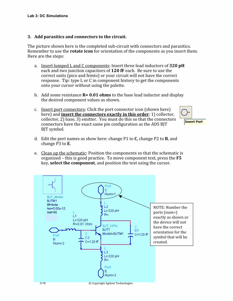
3. Addparasiticsandconnectorstothecircuit.
Thepictureshownhereisthecompletedsub‐circuitwithconnectorsandparasitics.Remembertousetherotateiconfororientationofthecomponentsasyouinsertthem.Herearethesteps:
a. InsertlumpedLandCcomponents:Insertthreeleadinductorsof320pHeachandtwojunctioncapacitorsof120fFeach.Besuretousethecorrectunits(picoandfemto)oryourcircuitwillnothavethecorrectresponse.Tip:typeLorCincomponenthistorytogetthecomponentsontoyourcursorwithoutusingthepalette.
b. AddsomeresistanceR=0.01ohmstothebaseleadinductoranddisplaythedesiredcomponentvaluesasshown.
c. Insertportconnectors:Clicktheportconnectoricon(shownhere)here)andinserttheconnectorsexactlyinthisorder:1)collector,collector,2)base,3)emitter.YoumustdothissothattheconnectorsconnectorshavetheexactsamepinconfigurationastheADSBJTBJTsymbol.
d. Edittheportnamesasshowhere:changeP1toC,changeP2toB,andchangeP3toE.
e. Cleanuptheschematic:Positionthecomponentssothattheschematicisorganized–thisisgoodpractice.Tomovecomponenttext,presstheF5key,selectthecomponent,andpositionthetextusingthecursor.
NOTE:Numbertheports(num=)exactlyasshownorthedevicewillnothavethecorrectorientationforthesymbolthatwillbecreated.
Lab 3: DC Simulations
33‐7©CopyrightAgilentTechnologies
2009
Defaultsymbol
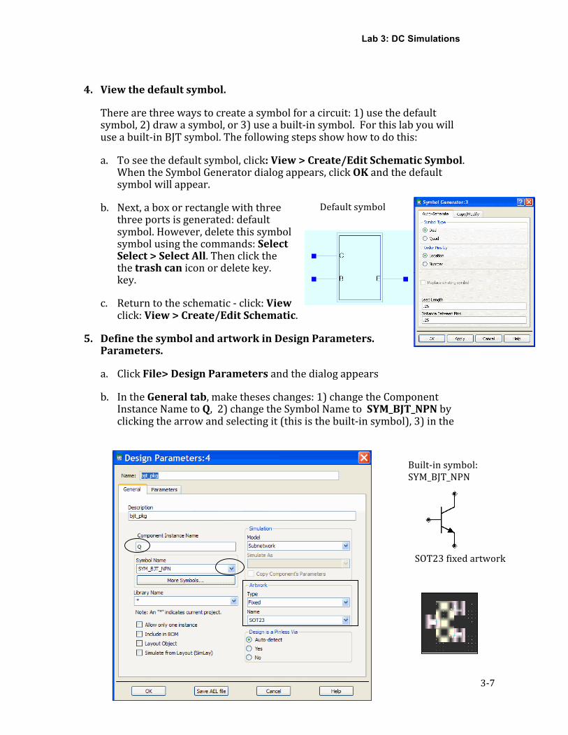
4. Viewthedefaultsymbol.
Therearethreewaystocreateasymbolforacircuit:1)usethedefaultsymbol,2)drawasymbol,or3)useabuilt‐insymbol.Forthislabyouwilluseabuilt‐inBJTsymbol.Thefollowingstepsshowhowtodothis:
a. Toseethedefaultsymbol,click:View>Create/EditSchematicSymbol.WhentheSymbolGeneratordialogappears,clickOKandthedefaultsymbolwillappear.
b. Next,aboxorrectanglewiththreethreeportsisgenerated:defaultsymbol.However,deletethissymbolsymbolusingthecommands:SelectSelect>SelectAll.Thenclickthethetrashcaniconordeletekey.key.
c. Returntotheschematic‐click:Viewclick:View>Create/EditSchematic.
5. DefinethesymbolandartworkinDesignParameters.Parameters.
a. ClickFile>DesignParametersandthedialogappears
b. IntheGeneraltab,maketheseschanges:1)changetheComponentInstanceNametoQ,2)changetheSymbolNametoSYM_BJT_NPNbyclickingthearrowandselectingit(thisisthebuilt‐insymbol),3)inthe
Built‐insymbol:SYM_BJT_NPN
SOT23fixedartwork
Lab 3: DC Simulations
3‐8 ©CopyrightAgilentTechnologies2009
Artworkfield,selectFixedandSOT23asshownhere.
c. ClickSaveAELFiletowritethesechangesbutdonotclosethisdialogyetbecauseyoustillneedtosetotherparameters.
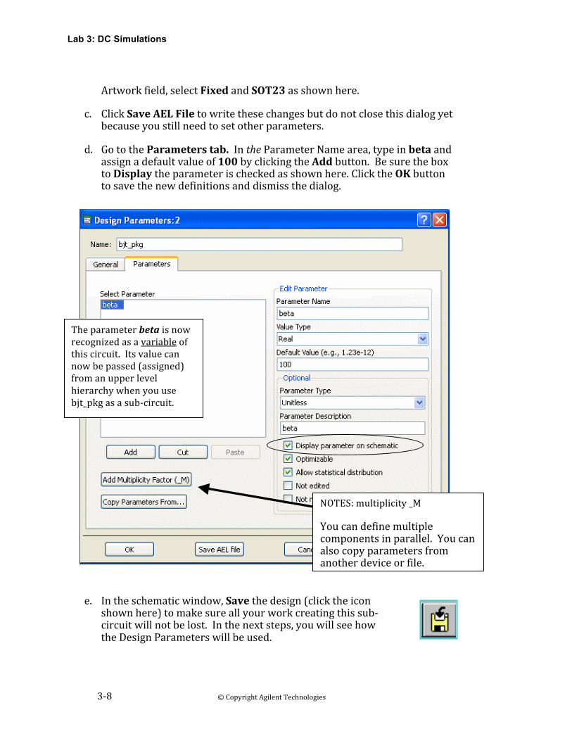
d. GototheParameterstab.IntheParameterNamearea,typeinbetaandassignadefaultvalueof100byclickingtheAddbutton.BesuretheboxtoDisplaytheparameterischeckedasshownhere.ClicktheOKbuttontosavethenewdefinitionsanddismissthedialog.
e. Intheschematicwindow,Savethedesign(clicktheiconshownhere)tomakesureallyourworkcreatingthissub‐circuitwillnotbelost.Inthenextsteps,youwillseehowtheDesignParameterswillbeused.
Theparameterbetaisnowrecognizedasavariableofthiscircuit.Itsvaluecannowbepassed(assigned)fromanupperlevelhierarchywhenyouusebjt_pkgasasub‐circuit.
NOTES:multiplicity_M
Youcandefinemultiplecomponentsinparallel.Youcanalsocopyparametersfromanotherdeviceorfile.
Lab 3: DC Simulations
33‐9©CopyrightAgilentTechnologies
2009
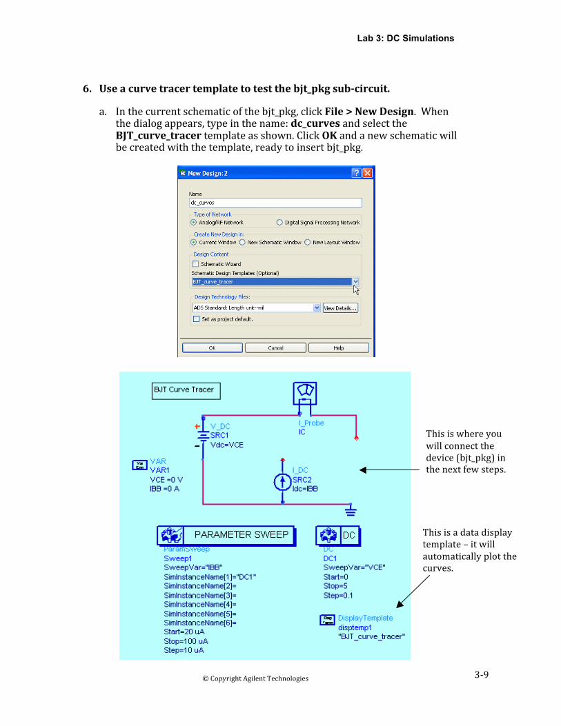
6. Useacurvetracertemplatetotestthebjt_pkgsubcircuit.
a. Inthecurrentschematicofthebjt_pkg,clickFile>NewDesign.Whenthedialogappears,typeinthename:dc_curvesandselecttheBJT_curve_tracertemplateasshown.ClickOKandanewschematicwillbecreatedwiththetemplate,readytoinsertbjt_pkg.
Thisisadatadisplaytemplate–itwillautomaticallyplotthecurves.
Thisiswhereyouwillconnectthedevice(bjt_pkg)inthenextfewsteps.
Lab 3: DC Simulations
3‐10 ©CopyrightAgilentTechnologies2009
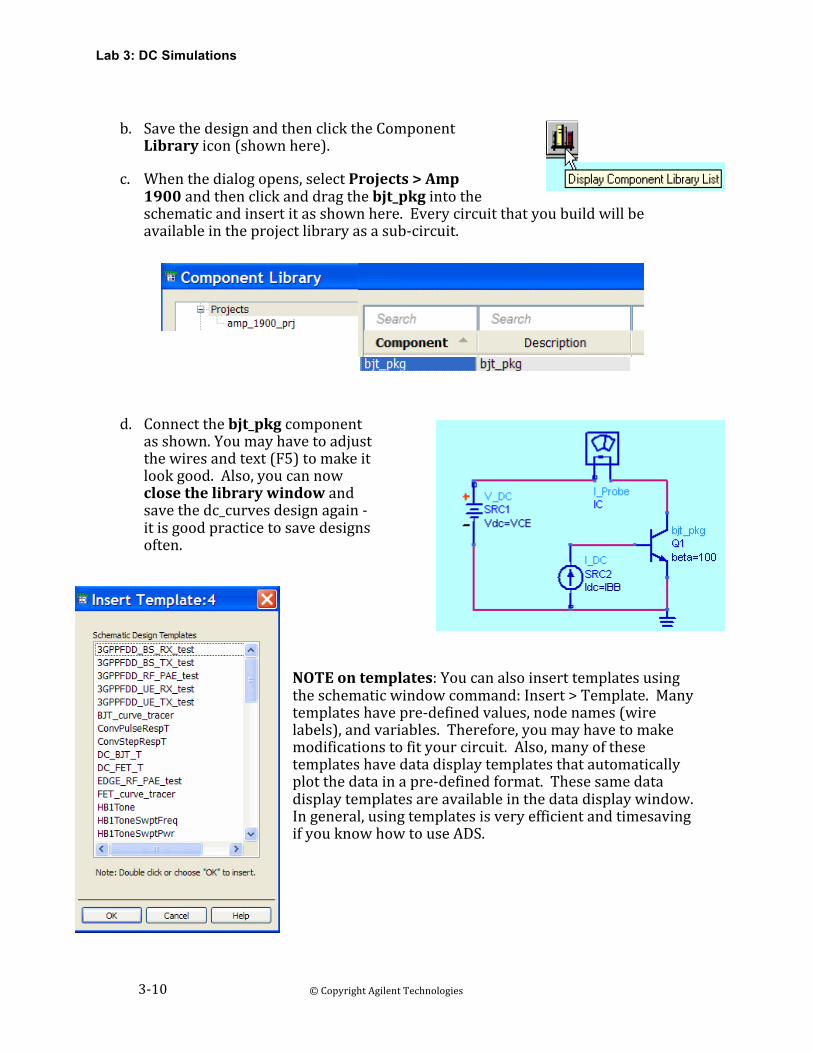
b. SavethedesignandthenclicktheComponentLibraryicon(shownhere).
c. Whenthedialogopens,selectProjects>Amp1900andthenclickanddragthebjt_pkgintotheschematicandinsertitasshownhere.Everycircuitthatyoubuildwillbeavailableintheprojectlibraryasasub‐circuit.
d. Connectthebjt_pkgcomponentasshown.Youmayhavetoadjustthewiresandtext(F5)tomakeitlookgood.Also,youcannowclosethelibrarywindowandsavethedc_curvesdesignagain‐itisgoodpracticetosavedesignsoften.
NOTEontemplates:Youcanalsoinserttemplatesusingtheschematicwindowcommand:Insert>Template.Manytemplateshavepre‐definedvalues,nodenames(wirelabels),andvariables.Therefore,youmayhavetomakemodificationstofityourcircuit.Also,manyofthesetemplateshavedatadisplaytemplatesthatautomaticallyplotthedatainapre‐definedformat.Thesesamedatadisplaytemplatesareavailableinthedatadisplaywindow.Ingeneral,usingtemplatesisveryefficientandtimesavingifyouknowhowtouseADS.
Lab 3: DC Simulations
33‐11©CopyrightAgilentTechnologies
2009
DCCurvesatbeta=100
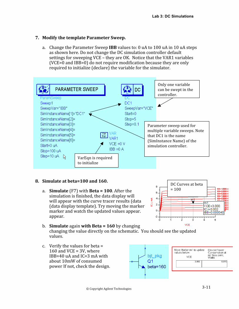
7. ModifythetemplateParameterSweep.
a. ChangetheParameterSweepIBBvaluesto:0uAto100uAin10uAstepsasshownhere.DonotchangetheDCsimulationcontrollerdefaultsettingsforsweepingVCE–theyareOK.NoticethattheVAR1variables(VCE=0andIBB=0)donotrequiremodificationbecausetheyareonlyrequiredtoinitialize(declare)thevariableforthesimulator.
8. Simulateatbeta=100and160.
a. Simulate(F7)withBeta=100.Afterthesimulationisfinished,thedatadisplaywillwillappearwiththecurvetracerresults(data(datadisplaytemplate).Trymovingthemarkermarkerandwatchtheupdatedvaluesappear.appear.
b. SimulateagainwithBeta=160bychangingchangingthevaluedirectlyontheschematic.Youshouldseetheupdatedvalues.
c. Verifythevaluesforbeta=160andVCE=3V,whereIBB=40uAandIC=3mAwithabout10mWofconsumedpowerIfnot,checkthedesign.
Parametersweepusedformultiplevariablesweeps.NotethatDC1isthename(SimInstanceName)ofthesimulationcontroller.
Onlyonevariablecanbesweptinthecontroller.
VarEqnisrequiredtoinitializevariables.
Lab 3: DC Simulations
3‐12 ©CopyrightAgilentTechnologies2009
StartupandWorkingdirectoryicons:
HideandShowicons:
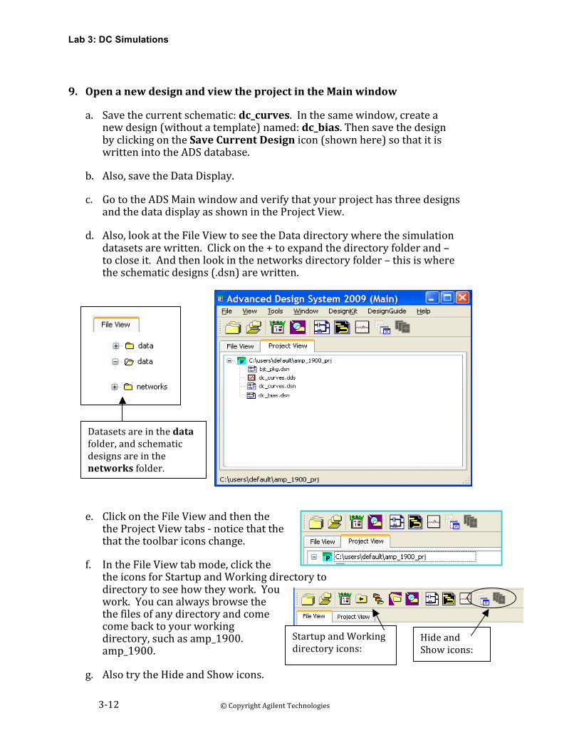
9. OpenanewdesignandviewtheprojectintheMainwindow
a. Savethecurrentschematic:dc_curves.Inthesamewindow,createanewdesign(withoutatemplate)named:dc_bias.ThensavethedesignbyclickingontheSaveCurrentDesignicon(shownhere)sothatitiswrittenintotheADSdatabase.
b. Also,savetheDataDisplay.
c. GototheADSMainwindowandverifythatyourprojecthasthreedesignsandthedatadisplayasshownintheProjectView.
d. Also,lookattheFileViewtoseetheDatadirectorywherethesimulationdatasetsarewritten.Clickonthe+toexpandthedirectoryfolderand–tocloseit.Andthenlookinthenetworksdirectoryfolder–thisiswheretheschematicdesigns(.dsn)arewritten.
e. ClickontheFileViewandthenthetheProjectViewtabs‐noticethatthethatthetoolbariconschange.
f. IntheFileViewtabmode,clickthetheiconsforStartupandWorkingdirectorytodirectorytoseehowtheywork.Youwork.Youcanalwaysbrowsethethefilesofanydirectoryandcomecomebacktoyourworkingdirectory,suchasamp_1900.amp_1900.
g. AlsotrytheHideandShowicons.
Datasetsareinthedatafolder,andschematicdesignsareinthenetworksfolder.

Lab 3: DC Simulations
33‐13©CopyrightAgilentTechnologies
2009
Lab 3: DC Simulations
3‐14 ©CopyrightAgilentTechnologies2009
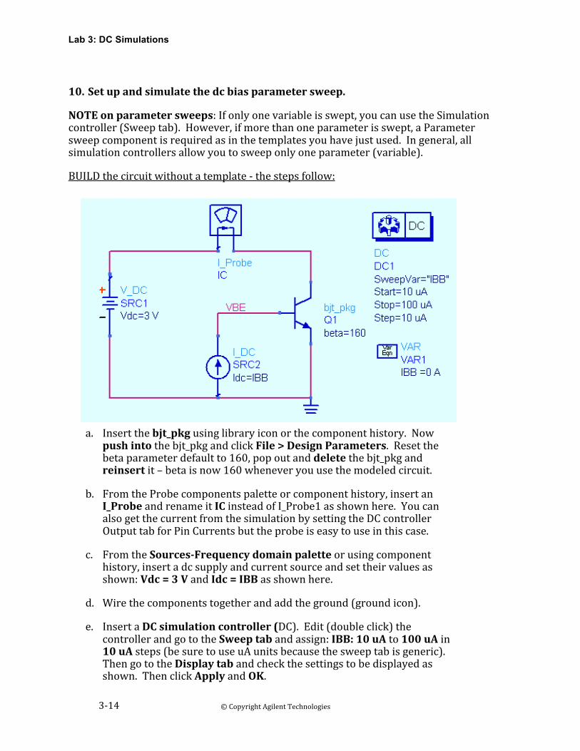
10. Setupandsimulatethedcbiasparametersweep.
NOTEonparametersweeps:Ifonlyonevariableisswept,youcanusetheSimulationcontroller(Sweeptab).However,ifmorethanoneparameterisswept,aParametersweepcomponentisrequiredasinthetemplatesyouhavejustused.Ingeneral,allsimulationcontrollersallowyoutosweeponlyoneparameter(variable).
BUILDthecircuitwithoutatemplate‐thestepsfollow:
a. Insertthebjt_pkgusinglibraryiconorthecomponenthistory.Nowpushintothebjt_pkgandclickFile>DesignParameters.Resetthebetaparameterdefaultto160,popoutanddeletethebjt_pkgandreinsertit–betaisnow160wheneveryouusethemodeledcircuit.
b. FromtheProbecomponentspaletteorcomponenthistory,insertanI_ProbeandrenameitICinsteadofI_Probe1asshownhere.YoucanalsogetthecurrentfromthesimulationbysettingtheDCcontrollerOutputtabforPinCurrentsbuttheprobeiseasytouseinthiscase.
c. FromtheSourcesFrequencydomainpaletteorusingcomponenthistory,insertadcsupplyandcurrentsourceandsettheirvaluesasshown:Vdc=3VandIdc=IBBasshownhere.
d. Wirethecomponentstogetherandaddtheground(groundicon).
e. InsertaDCsimulationcontroller(DC).Edit(doubleclick)thecontrollerandgototheSweeptabandassign:IBB:10uAto100uAin10uAsteps(besuretouseuAunitsbecausethesweeptabisgeneric).ThengototheDisplaytabandcheckthesettingstobedisplayedasshown.ThenclickApplyandOK.
Lab 3: DC Simulations
33‐15©CopyrightAgilentTechnologies
2009
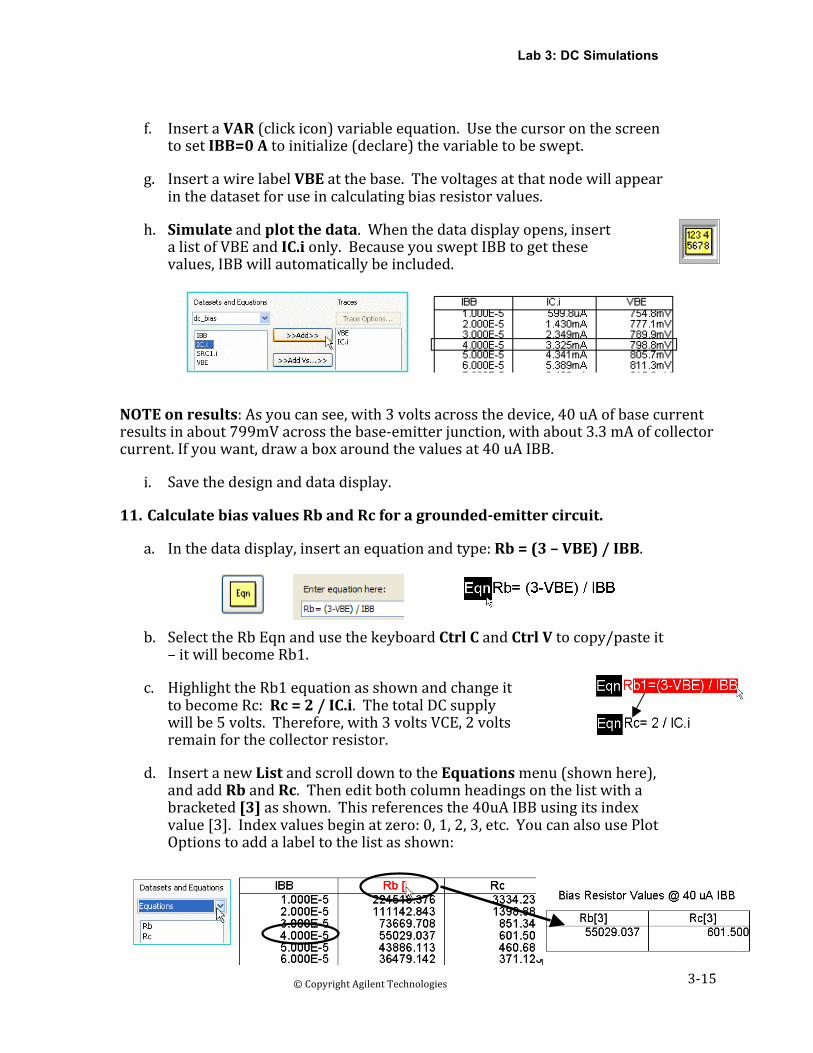
f. InsertaVAR(clickicon)variableequation.UsethecursoronthescreentosetIBB=0Atoinitialize(declare)thevariabletobeswept.
g. InsertawirelabelVBEatthebase.Thevoltagesatthatnodewillappearinthedatasetforuseincalculatingbiasresistorvalues.
h. Simulateandplotthedata.Whenthedatadisplayopens,insertalistofVBEandIC.ionly.BecauseyousweptIBBtogetthesevalues,IBBwillautomaticallybeincluded.
NOTEonresults:Asyoucansee,with3voltsacrossthedevice,40uAofbasecurrentresultsinabout799mVacrossthebase‐emitterjunction,withabout3.3mAofcollectorcurrent.Ifyouwant,drawaboxaroundthevaluesat40uAIBB.
i. Savethedesignanddatadisplay.
11. CalculatebiasvaluesRbandRcforagroundedemittercircuit.
a. Inthedatadisplay,insertanequationandtype:Rb=(3–VBE)/IBB.
b. SelecttheRbEqnandusethekeyboardCtrlCandCtrlVtocopy/pasteit–itwillbecomeRb1.
c. HighlighttheRb1equationasshownandchangeittobecomeRc:Rc=2/IC.i.ThetotalDCsupplywillbe5volts.Therefore,with3voltsVCE,2voltsremainforthecollectorresistor.
d. InsertanewListandscrolldowntotheEquationsmenu(shownhere),andaddRbandRc.Theneditbothcolumnheadingsonthelistwithabracketed[3]asshown.Thisreferencesthe40uAIBBusingitsindexvalue[3].Indexvaluesbeginatzero:0,1,2,3,etc.YoucanalsousePlotOptionstoaddalabeltothelistasshown:
Lab 3: DC Simulations
3‐16 ©CopyrightAgilentTechnologies2009
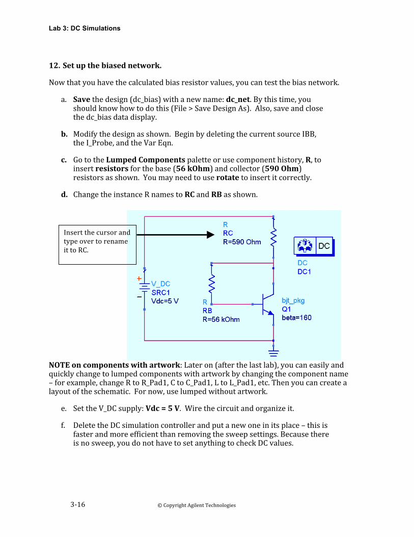
12. Setupthebiasednetwork.
Nowthatyouhavethecalculatedbiasresistorvalues,youcantestthebiasnetwork.
a. Savethedesign(dc_bias)withanewname:dc_net.Bythistime,youshouldknowhowtodothis(File>SaveDesignAs).Also,saveandclosethedc_biasdatadisplay.
b. Modifythedesignasshown.BeginbydeletingthecurrentsourceIBB,theI_Probe,andtheVarEqn.
c. GototheLumpedComponentspaletteorusecomponenthistory,R,toinsertresistorsforthebase(56kOhm)andcollector(590Ohm)resistorsasshown.Youmayneedtouserotatetoinsertitcorrectly.
d. ChangetheinstanceRnamestoRCandRBasshown.
NOTEoncomponentswithartwork:Lateron(afterthelastlab),youcaneasilyandquicklychangetolumpedcomponentswithartworkbychangingthecomponentname–forexample,changeRtoR_Pad1,CtoC_Pad1,LtoL_Pad1,etc.Thenyoucancreatealayoutoftheschematic.Fornow,uselumpedwithoutartwork.
e. SettheV_DCsupply:Vdc=5V.Wirethecircuitandorganizeit.
f. DeletetheDCsimulationcontrollerandputanewoneinitsplace–thisisfasterandmoreefficientthanremovingthesweepsettings.Becausethereisnosweep,youdonothavetosetanythingtocheckDCvalues.
InsertthecursorandtypeovertorenameittoRC.
Lab 3: DC Simulations
33‐17©CopyrightAgilentTechnologies
2009
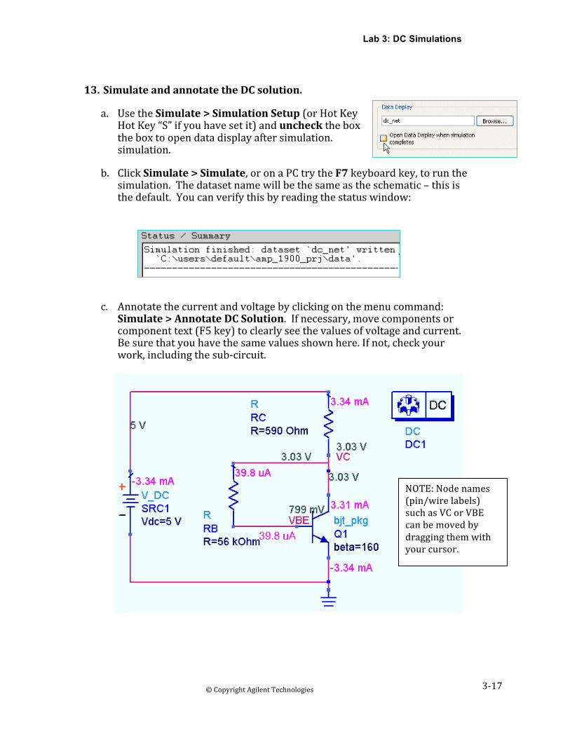
13. SimulateandannotatetheDCsolution.
a. UsetheSimulate>SimulationSetup(orHotKeyHotKey“S”ifyouhavesetit)andunchecktheboxtheboxtoopendatadisplayaftersimulation.simulation.
b. ClickSimulate>Simulate,oronaPCtrytheF7keyboardkey,torunthesimulation.Thedatasetnamewillbethesameastheschematic–thisisthedefault.Youcanverifythisbyreadingthestatuswindow:
c. Annotatethecurrentandvoltagebyclickingonthemenucommand:Simulate>AnnotateDCSolution.Ifnecessary,movecomponentsorcomponenttext(F5key)toclearlyseethevaluesofvoltageandcurrent.Besurethatyouhavethesamevaluesshownhere.Ifnot,checkyourwork,includingthesub‐circuit.
NOTE:Nodenames(pin/wirelabels)suchasVCorVBEcanbemovedbydraggingthemwithyourcursor.
Lab 3: DC Simulations
3‐18 ©CopyrightAgilentTechnologies2009
d. Cleartheannotation,click:Simulate>ClearDCAnnotationandthenSaveallyouwork.Closeallwindowsifnordoingtheoptionalstepsthatfollow.
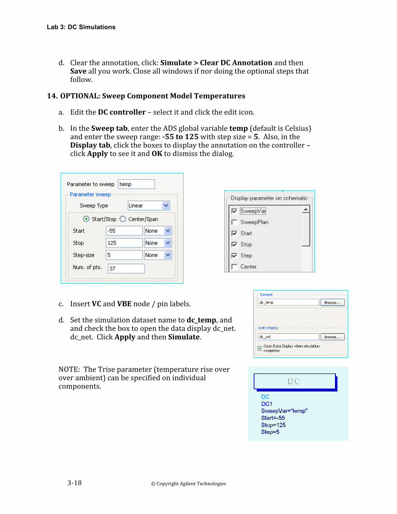
14. OPTIONAL:SweepComponentModelTemperatures
a. EdittheDCcontroller–selectitandclicktheediticon.
b. IntheSweeptab,entertheADSglobalvariabletemp(defaultisCelsius)andenterthesweeprange:55to125withstepsize=5.Also,intheDisplaytab,clicktheboxestodisplaytheannotationonthecontroller–clickApplytoseeitandOKtodismissthedialog.
c. InsertVCandVBEnode/pinlabels.
d. Setthesimulationdatasetnametodc_temp,andandchecktheboxtoopenthedatadisplaydc_net.dc_net.ClickApplyandthenSimulate.
NOTE:TheTriseparameter(temperatureriseoveroverambient)canbespecifiedonindividualcomponents.
Lab 3: DC Simulations
33‐19©CopyrightAgilentTechnologies
2009
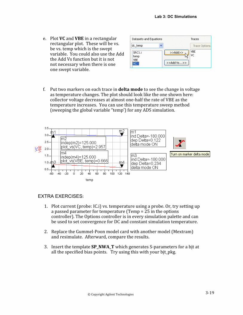
e. PlotVCandVBEinarectangularrectangularplot.Thesewillbevs.bevs.tempwhichisthesweptvariable.YoucouldalsousetheAddtheAddVsfunctionbutitisnotnotnecessarywhenthereisoneonesweptvariable.
f. Puttwomarkersoneachtraceindeltamodetoseethechangeinvoltageastemperaturechanges.Theplotshouldlookliketheoneshownhere:collectorvoltagedecreasesatalmostone‐halftherateofVBEasthetemperatureincreases.Youcanusethistemperaturesweepmethod(sweepingtheglobalvariable“temp’)foranyADSsimulation.
EXTRA EXERCISES:
1. Plotcurrent(probe:IC.i)vs.temperatureusingaprobe.Or,trysettingupapassedparameterfortemperature(Temp=25intheoptionscontroller).TheOptionscontrollerisineverysimulationpaletteandcanbeusedtosetconvergenceforDCandconstantsimulationtemperature.
2. ReplacetheGummel‐Poonmodelcardwithanothermodel(Mextram)andresimulate.Afterward,comparetheresults.
3. InsertthetemplateSP_NWA_TwhichgeneratesS‐parametersforabjtatallthespecifiedbiaspoints.Tryusingthiswithyourbjt_pkg.

Lab 3: DC Simulations
3‐20 ©CopyrightAgilentTechnologies2009