Embed Size (px)
Citation preview
LABORATORY MANUAL
ANALOG ELECTRONICS
B.TECH
3RD SEMESTER
DEPARTMENT OF ELECTRICAL ENGINEERING
JHARKHAND RAI UNIVERSITY KAMRE, RANCHI
JHARKHAND
EXPERIMENT NO:-01
AIM: To observe the characteristic of LED.
APPRATUS REQUIRED:
1) LED Kit 2) Multimeter 3) Connecting wire 4) Voltmeter (0-10v) 5) DC power supply 6) Rheostat
THEORY: When an electron comes down its higher energy level to lower
energy level, its limit energy in form of a photon. The energy of this
photon is equal to the energy gap between this to energy levels. When an
PN junction diodes is forward bias , current lows through the diode. Flows
of current through the semiconductor is caused by flow of free electron in
opposite direction of current and flow of holes in the direction of current,
Hence during flows of this charges carriers, there will be recombination .
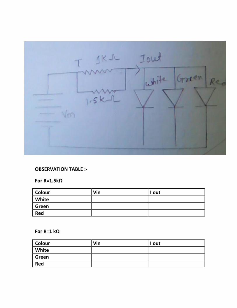
OBSERVATION TABLE :-
For R=1.5kΩ
Colour Vin I out
White
Green
Red
For R=1 kΩ
Colour Vin I out White
Green
Red
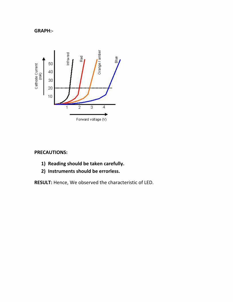
GRAPH:-
PRECAUTIONS:
1) Reading should be taken carefully. 2) Instruments should be errorless.
RESULT: Hence, We observed the characteristic of LED.
EXPERIMENT NO: 02
AIM: To observe the output waveforms of inverting and non-inverting amplifiers.
APPARATUS REQUIRED:
1. Op-amp-741(inverting and non-inverting operational amplifier) 2. CRO(cathode ray oscilloscope) 3. Connecting wire
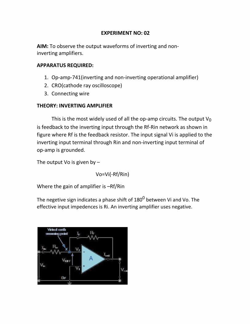
THEORY: INVERTING AMPLIFIER
This is the most widely used of all the op-amp circuits. The output V0
is feedback to the inverting input through the Rf-Rin network as shown in
figure where Rf is the feedback resistor. The input signal Vi is applied to the
inverting input terminal through Rin and non-inverting input terminal of
op-amp is grounded.
The output Vo is given by –
Vo=Vi(-Rf/Rin)
Where the gain of amplifier is –Rf/Rin
The negetive sign indicates a phase shift of 1800 between Vi and Vo. The
effective input impedences is Ri. An inverting amplifier uses negative.
NON-INVERTING AMPLIFIER
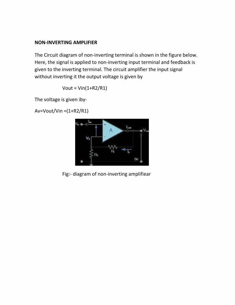
The Circuit diagram of non-inverting terminal is shown in the figure below.
Here, the signal is applied to non-inverting input terminal and feedback is
given to the inverting terminal. The circuit amplifier the input signal
without inverting it the output voltage is given by
Vout = Vin(1+R2/R1)
The voltage is given iby-
Av=Vout/Vin =(1+R2/R1)
Fig:- diagram of non-inverting amplifiear
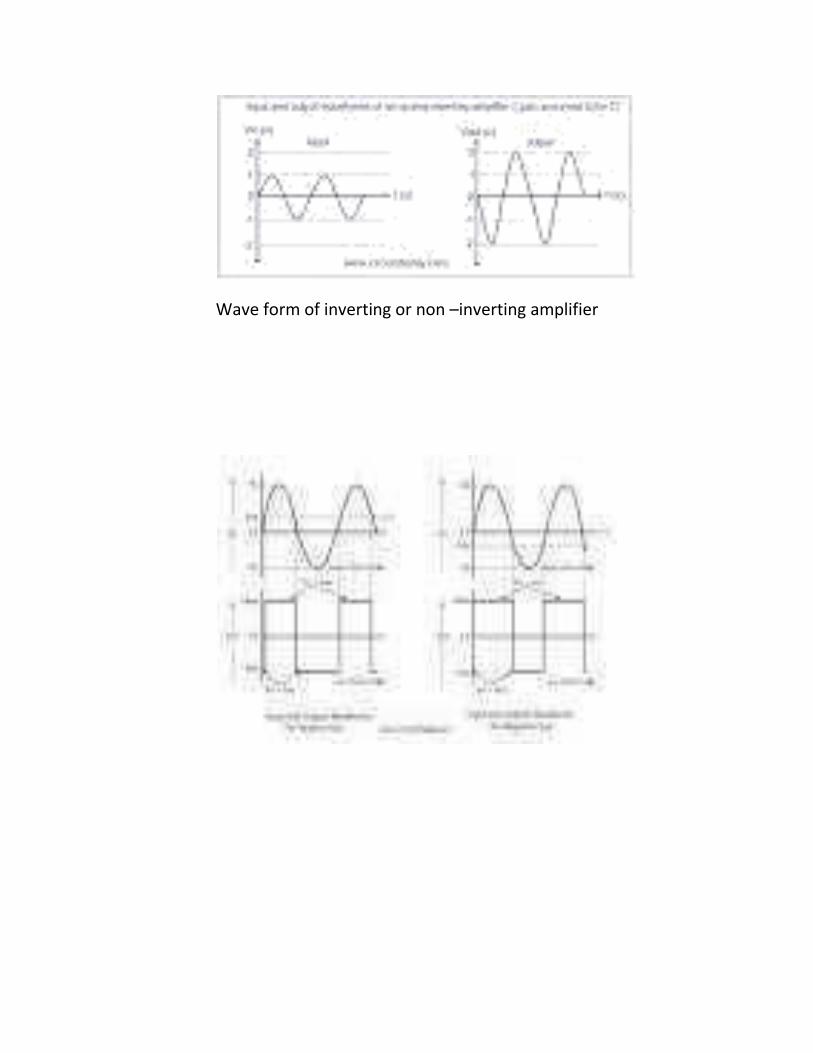
Wave form of inverting or non –inverting amplifier

PERCAUTION:
1) All the connection should be neat and tight. 2) The supply current should be proper.
RESULT: Hence, We observed the wave form of inverting and non-inverting amplifier.
EXPERIMNT NO: 03
AIM: To observe the output wave form of summing and difference amplifier.
APPRATUS REQUITRED:
1) Op-amp-741 kit 2) CRO 3) Connecting wire
THEORY:
SUMMER:- The summing circuit using op-amp as inverting mode
configuration with three input Va, Vb, Vc is shown in figure. The circuit act
as summing amplifier that means at the O/p, We get the addition of the
three input according to the circuit given in the figure O/p equation is as:
Va=Vb=Ov
I1 = (V1 – Va)/R1 = V1/R1
I2=(V2- Va)/R2 = V2/R2
I=(Va – Vo)/Rf = -Vo/Rf
Using KCL-
I= I1+I2
=-Vo/Rf = (V1/R1) + (V2/R2) If R1=R2
=-V0/Rf = (V1+V2)/R1
Vo = (-Rf/R1)V1+V2
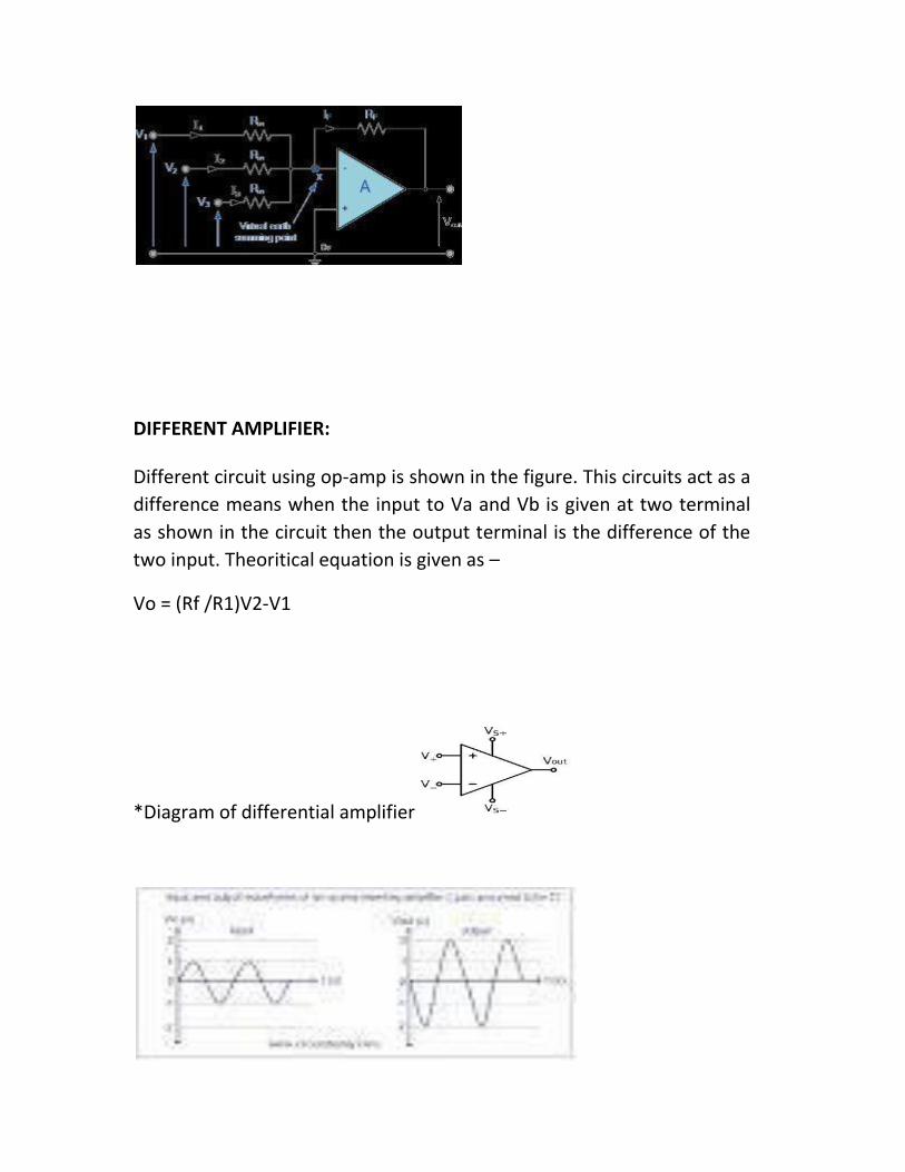
DIFFERENT AMPLIFIER:
Different circuit using op-amp is shown in the figure. This circuits act as a
difference means when the input to Va and Vb is given at two terminal
as shown in the circuit then the output terminal is the difference of the
two input. Theoritical equation is given as –
Vo = (Rf /R1)V2-V1
*Diagram of differential amplifier
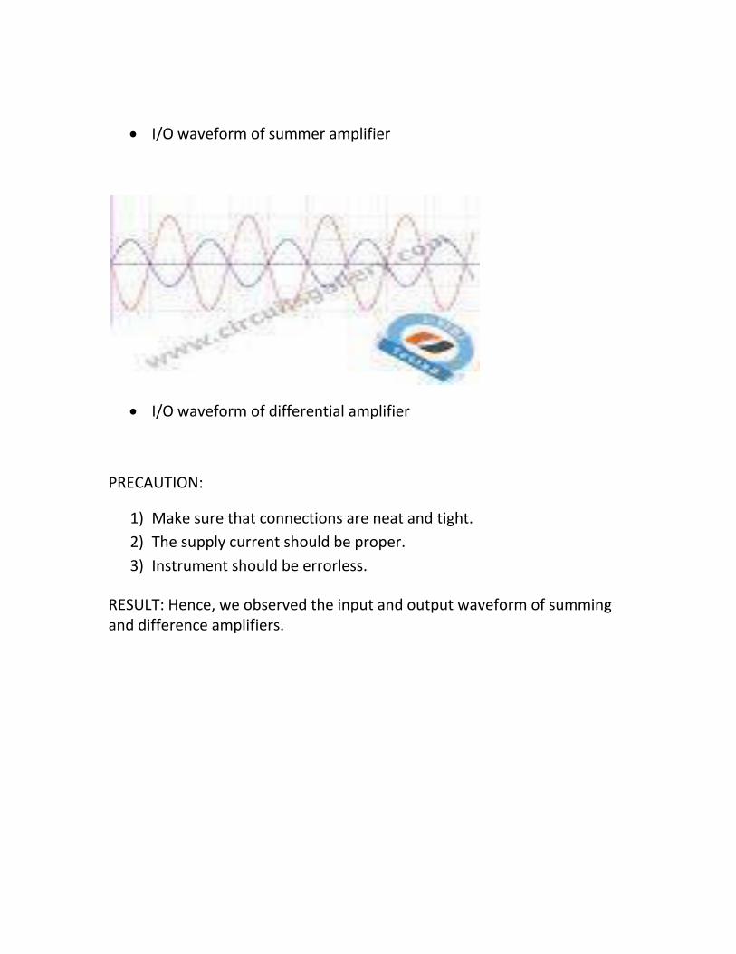
I/O waveform of summer amplifier
I/O waveform of differential amplifier
PRECAUTION:
1) Make sure that connections are neat and tight. 2) The supply current should be proper. 3) Instrument should be errorless.
RESULT: Hence, we observed the input and output waveform of summing and difference amplifiers.
EXPERIMENT NO: 04
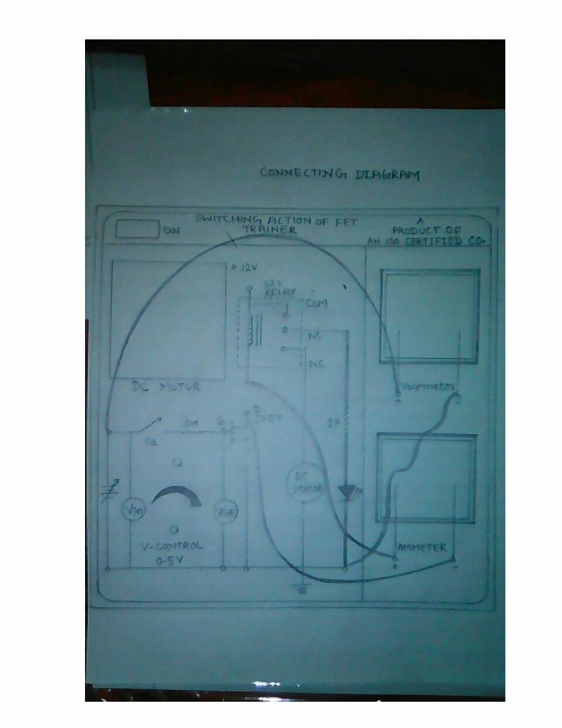
AIM: To Study the switching action of FET.
APPARATUS REQUIRED:
1) Switching action of FET Trainer. 2) Connecting wire.
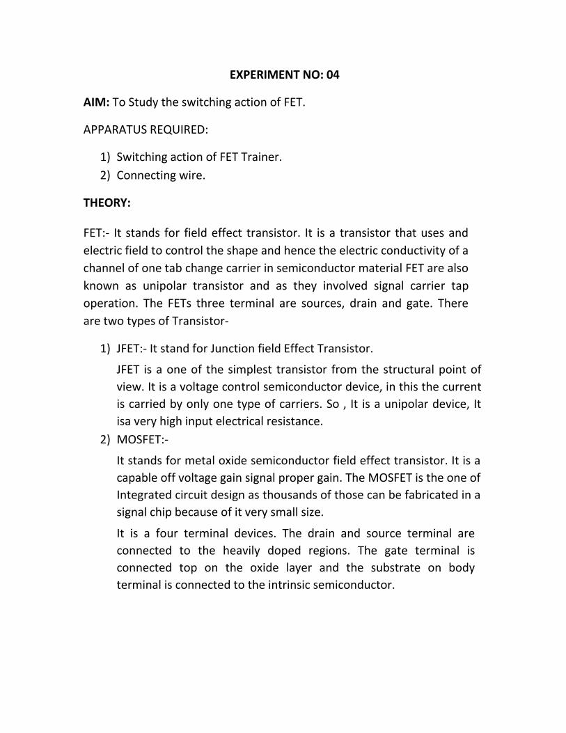
THEORY:
FET:- It stands for field effect transistor. It is a transistor that uses and
electric field to control the shape and hence the electric conductivity of a
channel of one tab change carrier in semiconductor material FET are also
known as unipolar transistor and as they involved signal carrier tap
operation. The FETs three terminal are sources, drain and gate. There
are two types of Transistor-
1) JFET:- It stand for Junction field Effect Transistor.
JFET is a one of the simplest transistor from the structural point of
view. It is a voltage control semiconductor device, in this the current
is carried by only one type of carriers. So , It is a unipolar device, It
isa very high input electrical resistance. 2) MOSFET:-
It stands for metal oxide semiconductor field effect transistor. It is a
capable off voltage gain signal proper gain. The MOSFET is the one of
Integrated circuit design as thousands of those can be fabricated in a
signal chip because of it very small size.
It is a four terminal devices. The drain and source terminal are
connected to the heavily doped regions. The gate terminal is
connected top on the oxide layer and the substrate on body
terminal is connected to the intrinsic semiconductor.
OBSERVATION TABLE:
When switch is off_
S.No Voltage I(Ammeter)
When Switch is on_
S.No Voltage I(Ammeter)
PRECAUTION:
1) When performing the experiment do not exceed the rating of the FET. This lead to damage FET.
2) Connect Voltmeter and ammeter with current polarities as shown
in the circuit diagram.
3) Do not Switch on the power supply unless the circuits connection are checked as per the circuit diagram
4) Properly identifies the sources, drain and gate terminal of
the transistor.
RESULT: Hence the switching action of FET is studied.
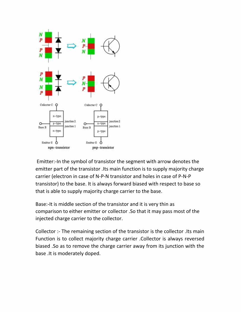
EXPERIMENT NO :05
AIM: To Study the switching action of BJT.
APPARATUS REQUIRED:-
1) Switching action of BJT trainer. 2) Connecting Wire.
THEORY:-
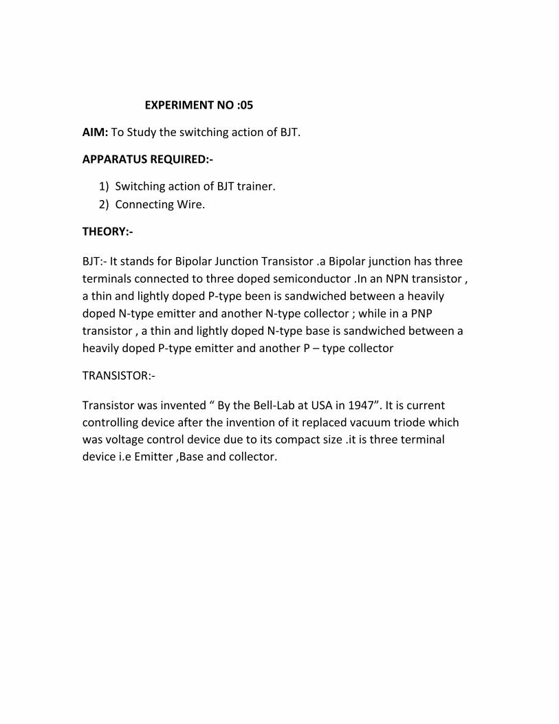
BJT:- It stands for Bipolar Junction Transistor .a Bipolar junction has three
terminals connected to three doped semiconductor .In an NPN transistor ,
a thin and lightly doped P-type been is sandwiched between a heavily
doped N-type emitter and another N-type collector ; while in a PNP
transistor , a thin and lightly doped N-type base is sandwiched between a
heavily doped P-type emitter and another P – type collector
TRANSISTOR:-
Transistor was invented “ By the Bell-Lab at USA in 1947”. It is current
controlling device after the invention of it replaced vacuum triode which
was voltage control device due to its compact size .it is three terminal
device i.e Emitter ,Base and collector.
Emitter:-In the symbol of transistor the segment with arrow denotes the
emitter part of the transistor .Its main function is to supply majority charge
carrier (electron in case of N-P-N transistor and holes in case of P-N-P
transistor) to the base. It is always forward biased with respect to base so
that is able to supply majority charge carrier to the base.
Base:-It is middle section of the transistor and it is very thin as
comparison to either emitter or collector .So that it may pass most of the
injected charge carrier to the collector.
Collector :- The remaining section of the transistor is the collector .Its main
Function is to collect majority charge carrier .Collector is always reversed
biased .So as to remove the charge carrier away from its junction with the
base .It is moderately doped.

OBERVATION TABLE:-
When switch is off mode
When switch is on mode
S.No Voltage(volt) Current(ampere)
1
2
3
4
S.No Voltage(volt) Current (ampere)
PRECAUTION:-
1) When performing the experiment do not exceed the rating of the BJT. This lead to damage BJT.
2) Connect Voltmeter and ammeter with current polarities as shown in
the circuit diagram.
3) Do not Switch on the power supply unless the circuits connection are checked as per the circuit diagram.
4) Properly identifies the Emitter, Base and Collector terminal of the transistor.
RESULT: - Hence, the switching action of BJT has been studied.
EXPERIMENT: - 06
AIM: - To study the output waveform of Filter.
APPARATUS REQUIRED:- 1) MATLAB Software
2)Computer
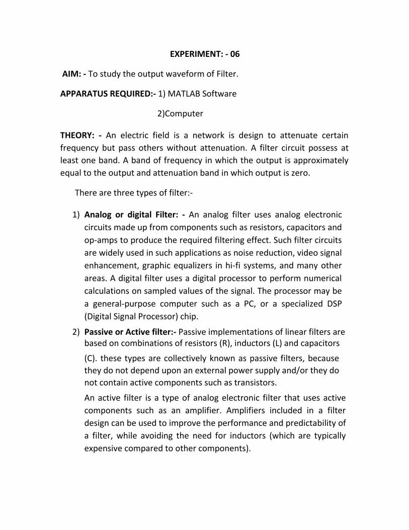
THEORY: - An electric field is a network is design to attenuate certain
frequency but pass others without attenuation. A filter circuit possess at
least one band. A band of frequency in which the output is approximately
equal to the output and attenuation band in which output is zero.
There are three types of filter:-
1) Analog or digital Filter: - An analog filter uses analog electronic
circuits made up from components such as resistors, capacitors and
op-amps to produce the required filtering effect. Such filter circuits
are widely used in such applications as noise reduction, video signal
enhancement, graphic equalizers in hi-fi systems, and many other
areas. A digital filter uses a digital processor to perform numerical
calculations on sampled values of the signal. The processor may be
a general-purpose computer such as a PC, or a specialized DSP
(Digital Signal Processor) chip.
2) Passive or Active filter:- Passive implementations of linear filters are based on combinations of resistors (R), inductors (L) and capacitors
(C). these types are collectively known as passive filters, because
they do not depend upon an external power supply and/or they do
not contain active components such as transistors.
An active filter is a type of analog electronic filter that uses active
components such as an amplifier. Amplifiers included in a filter
design can be used to improve the performance and predictability of
a filter, while avoiding the need for inductors (which are typically
expensive compared to other components).
3) Audio frequency or Radio frequency filter:- An RF Filter, or radio
frequency filter, is an electronic filter which is designed to operate
on signals in medium to extremely high frequencies. These ranges
are used in radio, television and wireless communications. Therefore
most RF devices include some kind of filtering on the signals
transmitted or received.
DIAGRAM:
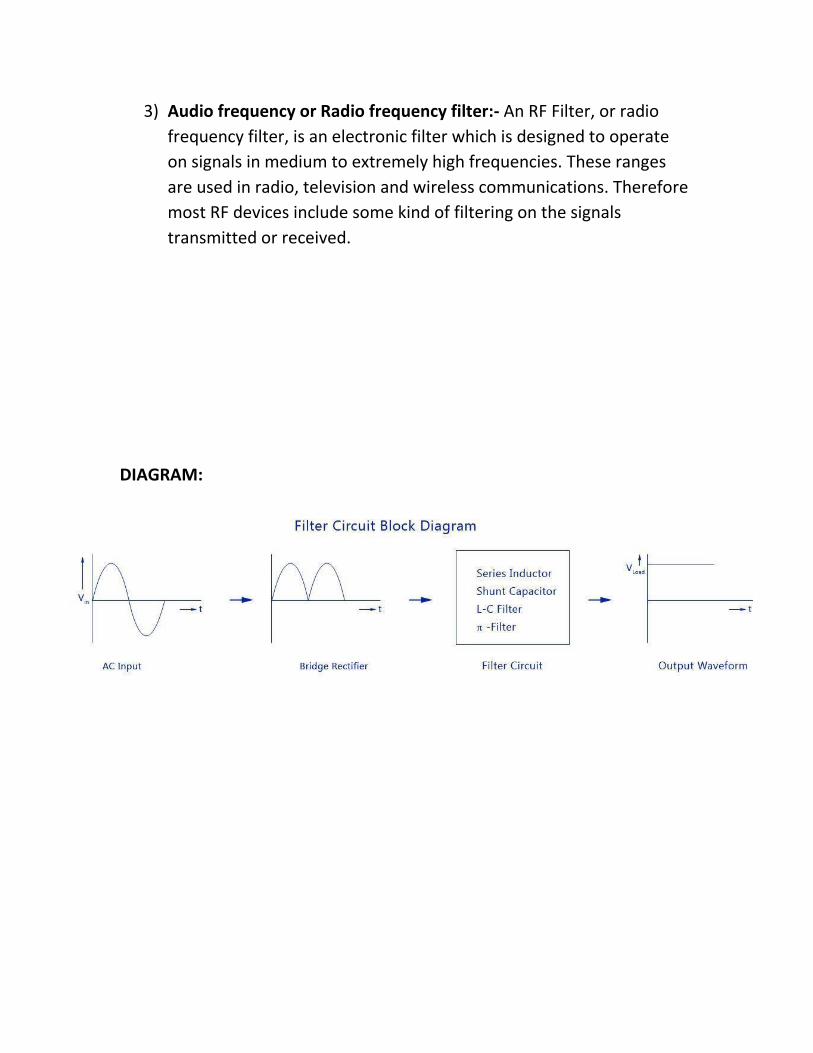
WAVEFORM:-

PRECAUTION: -
1) Make sure that connections are neat and tight. 2) The supply current should be proper. 3) Instrument should be errorless.
RESULT:- Hence, the output waveform of filter has been studied.
EXPERIMENT: 06
AIM: - To Study the characteristics of MOSFET in different modes.
APPARATUS REQUIRED:
1) MOSFET characteristics Apparatus
2) Connecting Wires
THEORY:-
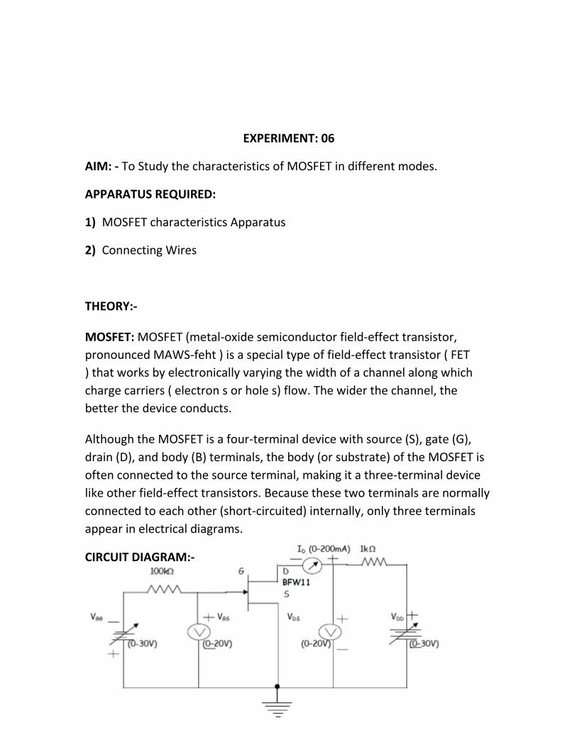
MOSFET: MOSFET (metal-oxide semiconductor field-effect transistor,
pronounced MAWS-feht ) is a special type of field-effect transistor ( FET
) that works by electronically varying the width of a channel along which
charge carriers ( electron s or hole s) flow. The wider the channel, the
better the device conducts.
Although the MOSFET is a four-terminal device with source (S), gate (G),
drain (D), and body (B) terminals, the body (or substrate) of the MOSFET is
often connected to the source terminal, making it a three-terminal device
like other field-effect transistors. Because these two terminals are normally
connected to each other (short-circuited) internally, only three terminals
appear in electrical diagrams.
CIRCUIT DIAGRAM:-
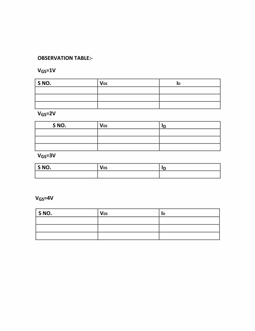
OBSERVATION TABLE:-
VGS=1V
S NO. VDS ID
VGS=2V
S NO. VDS ID
VGS=3V
S NO. VDS ID
VGS=4V
S NO. VDS ID
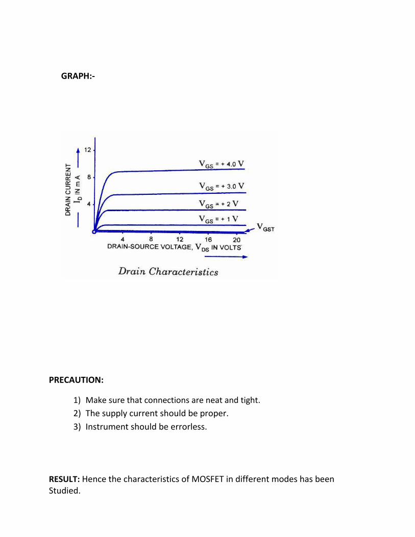
GRAPH:-
PRECAUTION:
1) Make sure that connections are neat and tight. 2) The supply current should be proper. 3) Instrument should be errorless.
RESULT: Hence the characteristics of MOSFET in different modes has been Studied.
EXPERIMENT NO:-08
CHARACTERISTICS OF PN JUNCTION DIODE
AIM: To study the PN junction diode characteristics under Forward & Reverse bias conditions.
APPARATUS REQUIRED-
1. PN Junction Kit
2. Ammeter,
3. Voltmeter,
4. Connecting wires,
5. Resistor
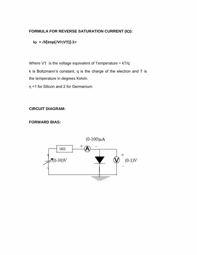
THEORY: A PN junction diode is a two terminal junction device. It conducts only in one direction (only on forward biasing). FORWARD BIAS:
On forward biasing, initially no current flows due to barrier potential. As the applied
potential exceeds the barrier potential the charge carriers gain sufficient energy to
cross the potential barrier and hence enter the other region. The holes, which are
majority carriers in the P-region, become minority carriers on entering the N-regions,
and electrons, which are the majority carriers in the N-region, become minority
carriers on entering the P-region. This injection of Minority carriers results in the
current flow, opposite to the direction of electron movement.
REVERSE BIAS:
On reverse biasing, the majority charge carriers are attracted towards the
terminals due to the applied potential resulting in the widening of the depletion
region. Since the charge carriers are pushed towards the terminals no current
flows in the device due to majority charge carriers. There will be some current in
the device due to the thermally generated minority carriers. The generation of
such carriers is independent of the applied potential and hence the current is
constant for all increasing reverse potential. This current is referred to as
Reverse Saturation Current (IO) and it increases with temperature. When the
applied reverse voltage is increased beyond the certain limit, it results in
breakdown. During breakdown, the diode current increases tremendously.
PROCEDURE:
FORWARD BIAS:
1. Connect the circuit as per the diagram.
2. Vary the applied voltage V in steps of 0.1V.
3. Note down the corresponding Ammeter readings If.
4. Plot a graph between Vf & If
OBSERVATIONS
1. Find the d.c (static) resistance = Vf / If.=
2. Find the a.c (dynamic) resistance r = δV / δI (r = V/ I) =
V2 −
V1 .=
I
2 − I1 3. Find the forward voltage drop = [Hint: it is equal to 0.7 for Si and 0.3
for Ge]=
REVERSE BIAS:
1. Connect the circuit as per the diagram.
2. Vary the applied voltage Vr in steps of 0.5V.
3. Note down the corresponding Ammeter readings Ir.
4. Plot a graph between Vr & Ir
5. Find the dynamic resistance r = δV / δI.
FORMULA FOR REVERSE SATURATION CURRENT (IO):
Io = ∂I/[exp(∂V/ηVT)]-1=
Where VT is the voltage equivalent of Temperature = kT/q
k is Boltzmann’s constant, q is the charge of the electron and T is
the temperature in degrees Kelvin.
η =1 for Silicon and 2 for Germanium
CIRCUIT DIAGRAM:
FORWARD BIAS:
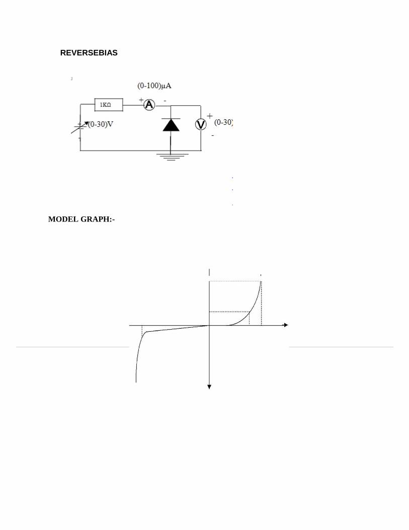
REVERSEBIAS MODEL GRAPH:-

TABULAR FORM:-
S.No. Voltage(Vf)(in V) Current(If)( µA) S.No. Voltage(Vr)(in V) Current(If)( µA)
RESULT: Thus, the V-I characteristics of P-N junction is verifi