Embed Size (px)
Citation preview
Laboratory Manual andSupplementary Notes
ECE 458: Computer SystemsLaboratory
Version 1.0
Dr. Sol RosenstarkDr. John Carpinelli
Department of Electrical and Computer EngineeringNew Jersey Institute of Technology
Newark, New Jersey
c© 2003New Jersey Institute of Technology
All rights reserved
Contents
Very Important General Notes iiProcurement of Components . . . . . . . . . . . . . . . . . . . . . . . iiProgramming GALs and EEPROMs . . . . . . . . . . . . . . . . . . . iii
EXPERIMENT 1: Introduction to the MC68000 Educational Com-puter Board and a Program For Data Input 1
EXPERIMENT 2: Data Record Sorting 6
EXPERIMENT 3: A Basic Mathematical Package for MultibyteNumbers 8
EXPERIMENT 4: An MC68000 Based Rudimentary Calculator 10
EXPERIMENT 5: Sequential Circuit Using Programmable Logic 12
EXPERIMENT 6: Event Driven Circuit 28
EXPERIMENT 7: Microsequencer Design 36
i

Very Important GeneralNotes
Procurement of Components
Each student has to take the initiative to obtain the following items, which willbe needed for experiments 5, 6 and 7.
• One GAL such as the Lattice 16V8.
• One 2816A EEPROM.
• One 74374 octal D-type latch (or CMOS equivalent).
• One 74298 quad 2-to-1 multiplexer with latched outputs.
• One debounced push button switch to simulate the system clock.
• Two DIP switches.
• Three LEDs and limiting resistors.
• Pencilbox kit (optional).
• Additional 74-series ICs based on the student’s design.
ii
Programming GALs and EEPROMs
In the \SP\BIN subdirectory type SP<ENT>.
• Type <F9> to select the programming of GALs or EEPROMs, and then<esc> to get out.
• Type <F7> and use < ∗ > <ENT> to select the device manufacturer,and then <esc> to get out.
• Type <F8> and use < ∗ > <ENT> to select the device number, and then<esc> to get out.
The proper data should now appear in the right middle of the screen. Use theFILE menu to load the file that you use to program the chip. Use the BUFFER,EDIT feature to verify the data that has been loaded. Go to the DEVICE screento program the chip. It’s self explanatory from here.
iii
EXPERIMENT 1:Introduction to theMC68000 EducationalComputer Board and aProgram For Data Input
Objectives
This experiment consists of two parts. In the first part, the student is intro-duced to the operation of the Motorola 68000 CPU based educational computerboard (ECB), the public domain communications package PROCOMM, and theAntonakos assembler. In the second part, a program has to be written whichwill accept data from the PC keyboard.
Equipment Needed
• MC68000 Educational Computer Board with RS232 communication cable,with 25 pin to 9 pin transition cable, as well as the SBC68K User’s Manualby Arnewsh Inc. These items are all available from the stockroom.
• The students should have in their possession, from the prerequisite Micro-processor course, the textbook The 68000 Microprocessor, Hardware andSoftware Principles and Applications, by James Antonakos, 4th Edition,Prentice Hall, 1999.
1
Background
The Motorola MC68000 Educational Computer Board includes:
• A 68000 microprocessor acting as the central processing unit.
• 16K-bytes of read only memory (ROM) containing a monitor program.
• 32K-bytes of read/write memory (RAM).
• Two serial RS232-C compatible communications ports, one for a terminaland one for a host.
• An audio tape serial I/O port and a parallel port.
• Reset and Abort function switches.
• The firmware has monitor, debug, one line assembly capability and amultiple line disassembly function.
• User programs can be uploaded to and downloaded from a laboratory PC.
The MC68000 ECB will be used with a PC as a host. To set up communi-cations between the PC and the MC68000 use the following procedure.
1. Connect the communications cable to the RS232 port COM1 of the PCand port 1 of the MC68000 ECB. Set the SBC serial communicationsspeed to 9600 or 19200 bits/second.
2. Use a DOS window on the PC and find the subdirectory C:\PROCOM.
3. Type P<ENT> to bring it up. You can use the CTRL-Z function to geta help menu.
4. Use ALT-P to set PROCOMM to the desired bit rate, no parity, 8 bitsand 1 stop bit.
5. To make sure that the SBC does not ruin your HEX files when theyare loaded, use ALT-S to set the ASCII TRANSFER OPTIONS for acharacter pacing of 500 millisec. All other parameters should be 0 and allother options should be answered in the negative. Save the settings whenyou exit.
6. Plug in the SBC and you should then have the prompt TUTOR 1.3 >which indicates that you have established communications between thePC and the ECB.
2

7. To upload a HEX file from the PC, at the SBC command line typeLO1<ENT>. The SBC will now be waiting for the HEX file transferto begin. Use the PgUp key to tell PROCOMM to send the file. Choosethe ASCII upload protocol and type, in the little box, the subdirectoryand the file name. That’s all there’s to it. (Question: Why do we useASCII file transfer ?)
Using The MC68000 Onboard Assembler
Though normally your programs will be assembled by the assembler on a PCin room 211F, the MC68000 has an onboard assembler. It is a line-at-a-timeassembler which means the programmer must compute all addresses. This as-sembler should be used for making small changes in a program. The user isreferred to the SBC68K User’s Manual for additional information on the use ofthis assembler.
Using The Antonakos ASM68K Assembler
The students should have acquired a reasonable familiarity with this assem-bler in the microprocessor course. This assembler should be found in theC:\ASM68K subdirectory on the computers in room 211F.
Preparing Your Programs For Assembly
Use any ASCII editor to prepare your program. Document type word processorssuch as Word or WordPerfect are not editors that produce ASCII files and shouldtherefore be avoided. DOS Edit or Notepad will do the job well enough.
A sample program, TEST, is given below:
; The SBC uses TRAP #14 to access many functions in the; MONITOR program which operates it. You have to inform; the TRAP #14 service routine what function you want it; to perform by putting a specific code-byte into D7.; These equates explain some of these code bytes.inchar equ 247 ;code for getting a keyboard charoutchar equ 248 ;code to send a char to the screenexit equ 228 ;code for a graceful exit to TUTOR
org $2000; This program inputs a character from the; keyboard until ’.’ is typed. The character; is then displayed on the monitor. The; characters typed are then stored in memory.getput lea.l storend,a6 ;point A6 to char storagenext move.b #inchar,d7 ;Get a character into D0.B
3
trap #14 ;using a MONITOR routinemove.b #outchar,d7;Put it on the screentrap #14move.b d0,-(a6) ;Store it going backwardscmpi.b #’.’,d0 ;See if char is a ’.’bne next ;No, then loop for moremove.b #exit,d7 ;Done, so exit gracefullytrap #14 ;to the MONITOR prompt
; Data storage area. We reserve only 20 bytes in RAM.stor ds.b 20storend
end getput ;This goes at the very end
Save this program in a file with extension .ASM, for example TEST.ASM.
Assembling Your Program
On the DOS prompt simply type A:>C:\ASM68K TEST. If errors are signaledat the end of assembly then examine the file TEST.LST to see what went wrong.Correct the errors in the TEST.ASM file and repeat the above procedure tillall the errors are eliminated. The file TEST.HEX is an ASCII file that can bedownloaded to the SBC for testing and can also be emulated with the Livadasand Ward simulator SIM68K.EXE.
The Experiment
1. Review Chapters 1–3, in Antonakos’s book.
2. What are the possible addressing modes of the MC68000 ? Give one ex-ample of each addressing mode in the form of an assembly language in-struction.
3. Read TRAP #14 for parameters #247 and #248 and #228 in the SBC68KUser’s Manual.
4. Create the file for the program TEST.ASM using an ASCII (non-document)editor. Assemble it using Antonakos’s ASM68K.EXE assembler. Find theLivadas and Ward simulator SIM68K.EXE. It is readily recognizable whenit is loaded into memory because it produces the sign-on display appearingbelow.
C:\>sim68kMC68000/ECB Simulator.Copyright (C) Livadas and Ward, 1992. Author Wayne WolfVersion 2.3SIM68000 2.3 >
4
5. This simulator is case sensitive and works with capital letter commandsonly. The commands are the same as for the ECB board as explainedin the SBC68K User’s Manual by Arnewsh Inc. The only difference isthat to load a file you simply type LO <TEST.HEX>. (For the SBC youwould type LO1 and then tell PROCOMM to upload the file.)
6. Observe that when you emulate the file TEST, the program crashes at acertain point. When does this happen and why ?
7. Modify the program TEST to include a test to make sure that the storedcharacters do not endanger the program itself. The program should, atthat point, stop accepting any more characters and put out a message onthe screen stating that an overflow has occurred.
8. Demonstrate the working version of the modified program TEST.
9. Using the MC68000 ECB on board assembler, write a delay loop for adelay of 1 sec. Only relative branch (Bcc) instructions should be used.The starting address of this code should be at 2000H.
10. Write routines to add, subtract and multiply two single byte numberswhich the user places on the stack using the TUTOR. The programs shouldPOP the parameters off the stack and place the computed result in registerD0.
11. Write a program that reads in data from the PC keyboard. The dataconsists of two parts:
(a) Name of a student. This may contain up to six alphabetic characters.The program must filter out all non-alphabetic characters and allcharacters after the first six alphabetic characters.
(b) ID number of a student. This must contain exactly nine digits. Theprogram must filter out all non-numeric characters and all charactersafter the first nine digits.
The data is to be stored in the memory as follows:
SMITH>883925333(0D)(0A) next record
and so on. This program should be capable of inputting data until theuser presses a ‘hot key’. A ‘hot key’ can be any one of the function keys,control keys or ESC, and pressing it indicates that the data entry is ter-minated. The program should then display all the data that has beeninputted before it exits. TRAP #14 handlers should be used for the in-put and output of data. Upload the data on your disk for later use inExperiment 2 and show the data to your instructor.
5
EXPERIMENT 2: DataRecord Sorting
Objectives
In this experiment, the MC68000 ECB is used to sort the records which werecreated in Experiment 1. The program should be able to sort the records bothalphabetically (according to name) or numerically (according to number).
Equipment Needed
• MC68000 Educational Computer Board with RS232 communication cable,with 25 pin to 9 pin transition cable, as well as the SBC68K User’s Manualby Arnewsh Inc. These items are all available from the stockroom.
• The students should have in their possession, from the prerequisite Micro-processor course, the textbook The 68000 Microprocessor, Hardware andSoftware Principles and Applications, by James Antonakos, 4th Edition,Prentice Hall, 1999.
Background
Data sorting is commonly done by computers for better presentation and struc-turing of the data to facilitate its search and retrieval. Sorting is a functionincluded in all database management programs. In Experiment 1, data recordswere entered into the ECB through the keyboard of the laboratory computer.It is desired to arrange this data in a logical order.
Chapter 6 of Antonakos’s book contains explanations of bucket sorting andbubble sorting algorithms. We are interested in one that can be implementedeasily. Efficiency is not an important criterion since our database has fewer thantwenty records
6
The Experiment
1. Write a commented assembly language program to implement the datasorting operation. It should be capable of sorting both alphabetically(according to name) and numerically (according to number).
2. Assemble and debug the program the so that it will sort the records cre-ated in Experiment 1. The sort should be done in two ways: The programshould sort the records in ascending order. It should display both out-puts, that is records sorted alphabetically and records sorted numerically.Assemble and test your program. Get a printout of the output and attachit to your report.
3. Change the program so that it sorts data in descending order instead ofascending order. Get a printout of this and attach it to your report.
7

EXPERIMENT 3: A BasicMathematical Package forMultibyte Numbers
Objectives
In this experiment we develop a basic mathematical package for multibyte BCDnumbers. The operations which will be possible using this package will beaddition and multiplication. This experiment consists of two parts. In the firstpart a program for addition will be implemented. In the second part a programfor multiplication will be implemented.
Equipment Needed
• MC68000 Educational Computer Board with RS232 communication cable,with 25 pin to 9 pin transition cable, as well as the SBC68K User’s Manualby Arnewsh Inc. These items are all available from the stockroom.
• The students should have in their possession, from the prerequisite Micro-processor course, the textbook The 68000 Microprocessor, Hardware andSoftware Principles and Applications, by James Antonakos, 4th Edition,Prentice Hall, 1999.
Background
A mathematical package is normally developed for microprocessor based systemsas a library of subroutines. Each subroutine has a different function, such asaddition, subtraction, multiplication and division. There are different sets ofsubroutines for integers, real numbers and floating point numbers. Subroutinescan also be developed for other functions, such as sines, cosines, tangents etc.
8
These subroutines, once developed, can then be called from any program. Thiscuts down the development time of the programs. These subroutines should bewell documented and the registers and memory used for parameter passing andreturn of results should be similar for all such subroutines.
The Experiment
1. List the instructions used for mathematical operations on BCD numbersfor the MC68000.
2. Write commented assembly programs and include flow charts for the im-plementation of routines for addition and multiplication of multibyte BCDpositive integers. The number of bytes in a number are stored in one reg-ister and a pointer to the start of the number is stored in another register.The second number is also similarly stored with different registers for thenumber of bytes and the pointer. All these routines should return theanswer in a similar format in two registers. This problem is greatly sim-plified if you use a similar structure for all these routines. Multiplicationcan be done by any algorithm, the simplest being multiplication by itera-tive addition. Minimize the number of scratch registers. Save and restoreall registers you use.
3. Assemble and debug the routines for addition and multiplication. Testthe routines and attach two examples of each operation.
4. Attach an example for addition where a carry is generated.
9
EXPERIMENT 4: AnMC68000 BasedRudimentary Calculator
Objectives
In this experiment a rudimentary calculator is developed. The subroutines de-veloped in the earlier experiment can be used with modifications if necessary.The operations which will be performed by this calculator are addition, sub-traction and multiplication.
Equipment Needed
• MC68000 Educational Computer Board with RS232 communication cable,with 25 pin to 9 pin transition cable, as well as the SBC68K User’s Manualby Arnewsh Inc. These items are all available from the stockroom.
• The students should have in their possession, from the prerequisite Micro-processor course, the textbook The 68000 Microprocessor, Hardware andSoftware Principles and Applications, by James Antonakos, 4th Edition,Prentice Hall, 1999.
Background
This experiment is a practical application of the techniques learned in the earlierexperiments. The mathematical package developed in experiment 3 will bestreamlined for ease of user input and output. TRAP #14 handlers will be usedfor data input and output.
10

The Experiment
1. Write a program to implement a rudimentary calculator for positive BCDnumbers. The calculator should work as follows.
(a) All the keyboard entries described below should be echoed on themonitor.
(b) The first operand should be typed in from the keyboard. It shouldbe followed by a space typed on the keyboard.
(c) The operation to be carried out should be typed next followed by aspace. This operation can be +, − or ∗.
(d) The second operand should be typed in followed by <ENT>. Thecalculation should now be performed and the result should be dis-played on the next line.
An example is shown below.2138< SP > + < SP > 9528 < ENT >11666
The operands will be positive integers up to 15 digits long.
2. Your code should handle illegal key intries in a sensible way.
3. Get the printout of one example of each operation.
4. Explain briefly how you would implement a function like sin(x), cos(x)and tan(x), where x is in degrees.
11
EXPERIMENT 5:Sequential Circuit UsingProgrammable Logic
Objectives
The objective of this lab is to take the student through the design of a sequentialcircuit in an implementation utilizing a programmable logic device.
Preparation
Review the material pertaining to sequential logic in Logic and Computer DesignFundamentals, by M. Morris Mano and Charles R. Kime, Prentice Hall, 1997.
Requisite Equipment and Reference
• One GAL such as the Lattice 16V8-25.
• The dice-tosser jig for testing the GAL.
• Logic and Computer Design Fundamentals, by M. Morris Mano and CharlesR. Kime, Prentice Hall, 1997.
Background
Introduction to GAL
When designing digital circuits, the question is often asked: “Is it possible to re-duce the chip count by utilizing a more advanced IC technology?” The technol-ogy in question is generally referred to as ASIC (Application Specific Integrated
12
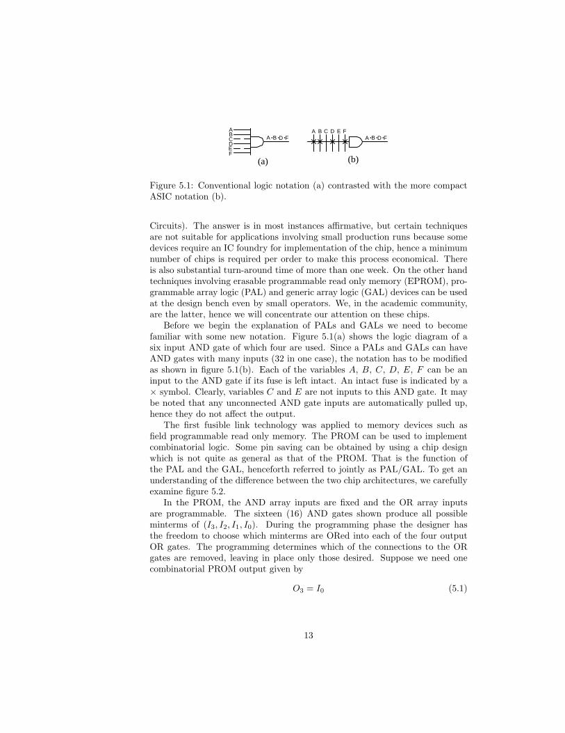
B A B . F . D .
A
C D E F
B A B . F . D . A C D E F
(a) (b)
Figure 5.1: Conventional logic notation (a) contrasted with the more compactASIC notation (b).
Circuits). The answer is in most instances affirmative, but certain techniquesare not suitable for applications involving small production runs because somedevices require an IC foundry for implementation of the chip, hence a minimumnumber of chips is required per order to make this process economical. Thereis also substantial turn-around time of more than one week. On the other handtechniques involving erasable programmable read only memory (EPROM), pro-grammable array logic (PAL) and generic array logic (GAL) devices can be usedat the design bench even by small operators. We, in the academic community,are the latter, hence we will concentrate our attention on these chips.
Before we begin the explanation of PALs and GALs we need to becomefamiliar with some new notation. Figure 5.1(a) shows the logic diagram of asix input AND gate of which four are used. Since a PALs and GALs can haveAND gates with many inputs (32 in one case), the notation has to be modifiedas shown in figure 5.1(b). Each of the variables A, B, C, D, E, F can be aninput to the AND gate if its fuse is left intact. An intact fuse is indicated by a× symbol. Clearly, variables C and E are not inputs to this AND gate. It maybe noted that any unconnected AND gate inputs are automatically pulled up,hence they do not affect the output.
The first fusible link technology was applied to memory devices such asfield programmable read only memory. The PROM can be used to implementcombinatorial logic. Some pin saving can be obtained by using a chip designwhich is not quite as general as that of the PROM. That is the function ofthe PAL and the GAL, henceforth referred to jointly as PAL/GAL. To get anunderstanding of the difference between the two chip architectures, we carefullyexamine figure 5.2.
In the PROM, the AND array inputs are fixed and the OR array inputsare programmable. The sixteen (16) AND gates shown produce all possibleminterms of (I3, I2, I1, I0). During the programming phase the designer hasthe freedom to choose which minterms are ORed into each of the four outputOR gates. The programming determines which of the connections to the ORgates are removed, leaving in place only those desired. Suppose we need onecombinatorial PROM output given by
O3 = I0 (5.1)
13
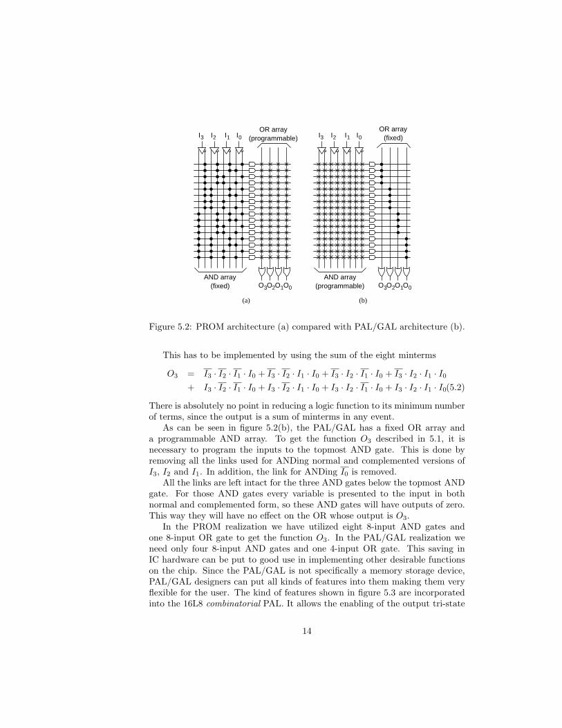
OR array (programmable) I 1 I 0 I 2 I 3
O 0 O 1 O 2 O 3
AND array (fixed)
OR array (fixed) I 1 I 0 I 2 I 3
O 0 O 1 O 2 O 3
AND array (programmable)
(a) (b)
Figure 5.2: PROM architecture (a) compared with PAL/GAL architecture (b).
This has to be implemented by using the sum of the eight minterms
O3 = I3 · I2 · I1 · I0 + I3 · I2 · I1 · I0 + I3 · I2 · I1 · I0 + I3 · I2 · I1 · I0
+ I3 · I2 · I1 · I0 + I3 · I2 · I1 · I0 + I3 · I2 · I1 · I0 + I3 · I2 · I1 · I0(5.2)
There is absolutely no point in reducing a logic function to its minimum numberof terms, since the output is a sum of minterms in any event.
As can be seen in figure 5.2(b), the PAL/GAL has a fixed OR array anda programmable AND array. To get the function O3 described in 5.1, it isnecessary to program the inputs to the topmost AND gate. This is done byremoving all the links used for ANDing normal and complemented versions ofI3, I2 and I1. In addition, the link for ANDing I0 is removed.
All the links are left intact for the three AND gates below the topmost ANDgate. For those AND gates every variable is presented to the input in bothnormal and complemented form, so these AND gates will have outputs of zero.This way they will have no effect on the OR whose output is O3.
In the PROM realization we have utilized eight 8-input AND gates andone 8-input OR gate to get the function O3. In the PAL/GAL realization weneed only four 8-input AND gates and one 4-input OR gate. This saving inIC hardware can be put to good use in implementing other desirable functionson the chip. Since the PAL/GAL is not specifically a memory storage device,PAL/GAL designers can put all kinds of features into them making them veryflexible for the user. The kind of features shown in figure 5.3 are incorporatedinto the 16L8 combinatorial PAL. It allows the enabling of the output tri-state
14
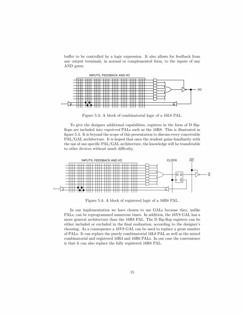
buffer to be controlled by a logic expression. It also allows for feedback fromany output terminals, in normal or complemented form, to the inputs of anyAND gates.
I/O
I
INPUTS, FEEDBACK AND I/O
Figure 5.3: A block of combinatorial logic of a 16L8 PAL.
To give the designer additional capabilities, registers in the form of D flip-flops are included into registered PALs such as the 16R8. This is illustrated infigure 5.4. It is beyond the scope of this presentation to discuss every conceivablePAL/GAL architecture. It is hoped that once the student gains familiarity withthe use of one specific PAL/GAL architecture, the knowledge will be transferableto other devices without much difficulty.
I
INPUTS, FEEDBACK AND I/O
D Q
Q
OC CLOCK
Q
Figure 5.4: A block of registered logic of a 16R8 PAL.
In our implementation we have chosen to use GALs because they, unlikePALs, can be reprogrammed numerous times. In addition, the 16V8 GAL has amore general architecture than the 16R8 PAL. The D flip-flop registers can beeither included or excluded in the final realization, according to the designer’schoosing. As a consequence a 16V8 GAL can be used to replace a great numberof PALs. It can replace the purely combinatorial 16L8 PAL as well as the mixedcombinatorial and registered 16R4 and 16R6 PALs. In our case the convenienceis that it can also replace the fully registered 16R8 PAL.
15
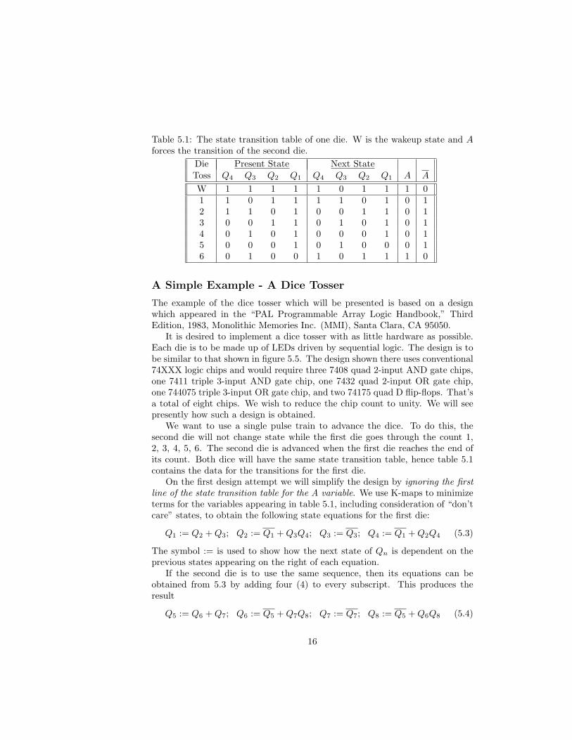
Table 5.1: The state transition table of one die. W is the wakeup state and Aforces the transition of the second die.
Die Present State Next StateToss Q4 Q3 Q2 Q1 Q4 Q3 Q2 Q1 A A
W 1 1 1 1 1 0 1 1 1 01 1 0 1 1 1 1 0 1 0 12 1 1 0 1 0 0 1 1 0 13 0 0 1 1 0 1 0 1 0 14 0 1 0 1 0 0 0 1 0 15 0 0 0 1 0 1 0 0 0 16 0 1 0 0 1 0 1 1 1 0
A Simple Example - A Dice Tosser
The example of the dice tosser which will be presented is based on a designwhich appeared in the “PAL Programmable Array Logic Handbook,” ThirdEdition, 1983, Monolithic Memories Inc. (MMI), Santa Clara, CA 95050.
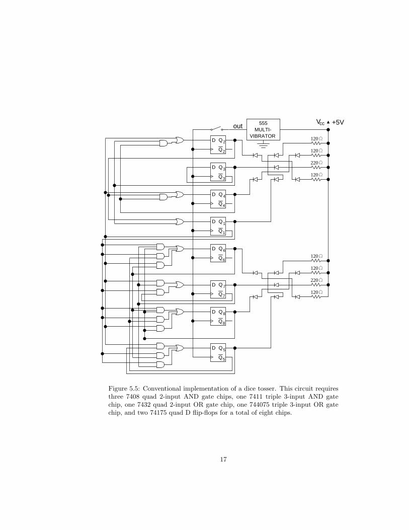
It is desired to implement a dice tosser with as little hardware as possible.Each die is to be made up of LEDs driven by sequential logic. The design is tobe similar to that shown in figure 5.5. The design shown there uses conventional74XXX logic chips and would require three 7408 quad 2-input AND gate chips,one 7411 triple 3-input AND gate chip, one 7432 quad 2-input OR gate chip,one 744075 triple 3-input OR gate chip, and two 74175 quad D flip-flops. That’sa total of eight chips. We wish to reduce the chip count to unity. We will seepresently how such a design is obtained.
We want to use a single pulse train to advance the dice. To do this, thesecond die will not change state while the first die goes through the count 1,2, 3, 4, 5, 6. The second die is advanced when the first die reaches the end ofits count. Both dice will have the same state transition table, hence table 5.1contains the data for the transitions for the first die.
On the first design attempt we will simplify the design by ignoring the firstline of the state transition table for the A variable. We use K-maps to minimizeterms for the variables appearing in table 5.1, including consideration of “don’tcare” states, to obtain the following state equations for the first die:
Q1 := Q2 + Q3; Q2 := Q1 + Q3Q4; Q3 := Q3; Q4 := Q1 + Q2Q4 (5.3)
The symbol := is used to show how the next state of Qn is dependent on theprevious states appearing on the right of each equation.
If the second die is to use the same sequence, then its equations can beobtained from 5.3 by adding four (4) to every subscript. This produces theresult
Q5 := Q6 + Q7; Q6 := Q5 + Q7Q8; Q7 := Q7; Q8 := Q5 + Q6Q8 (5.4)
16
555 MULTI-
VIBRATOR
out +5V
D Q 2
Q 2
D Q 3
Q 3
D Q 4
Q 4
D Q 1
Q 1
D Q 6
Q 6
D Q 7
Q 7
D Q 8
Q 8
D Q 5
Q 5
V cc
120
220
120
120
120
220
120
120
Figure 5.5: Conventional implementation of a dice tosser. This circuit requiresthree 7408 quad 2-input AND gate chips, one 7411 triple 3-input AND gatechip, one 7432 quad 2-input OR gate chip, one 744075 triple 3-input OR gatechip, and two 74175 quad D flip-flops for a total of eight chips.
17
Again, we ignore the first line of table 5.1, and obtain the equation for thetransition variable A,
A = Q1 (5.5)
And while we are at it, we perform an independent determination for its com-plement A to obtain,
A = Q1 (5.6)
Since we do not intend to use two separate clocks, we will simply have thefirst die count up from 1 to 6 then back to 1 again. When the first die goes fromstate 6 back to state 1, the second die will be incremented. We want Qn to stayin its current state when A = 0 and to make a transition when A = 1. Below,the state equations given previously for the second die have been modified toreflect this fact.
In summary the state equations for both dice are:
Q1 := Q2 + Q3 (5.7)Q2 := Q1 + Q3Q4 (5.8)Q3 := Q3 (5.9)Q4 := Q1 + Q2Q4 (5.10)Q5 := AQ5 + A(Q6 + Q7) (5.11)Q6 := AQ6 + A(Q5 + Q7Q8) (5.12)Q7 := AQ7 + A(Q7) (5.13)Q8 := AQ8 + A(Q5 + Q6Q8) (5.14)
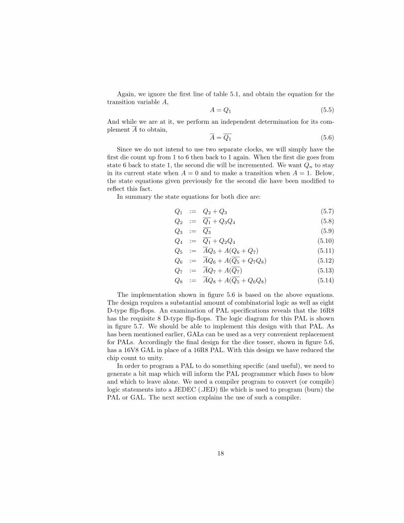
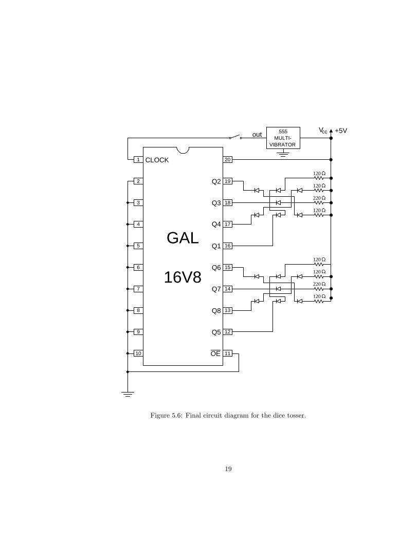
The implementation shown in figure 5.6 is based on the above equations.The design requires a substantial amount of combinatorial logic as well as eightD-type flip-flops. An examination of PAL specifications reveals that the 16R8has the requisite 8 D-type flip-flops. The logic diagram for this PAL is shownin figure 5.7. We should be able to implement this design with that PAL. Ashas been mentioned earlier, GALs can be used as a very convenient replacementfor PALs. Accordingly the final design for the dice tosser, shown in figure 5.6,has a 16V8 GAL in place of a 16R8 PAL. With this design we have reduced thechip count to unity.
In order to program a PAL to do something specific (and useful), we need togenerate a bit map which will inform the PAL programmer which fuses to blowand which to leave alone. We need a compiler program to convert (or compile)logic statements into a JEDEC (.JED) file which is used to program (burn) thePAL or GAL. The next section explains the use of such a compiler.
18
19
17
18
16
15
14
13
12
20
11
9
7
8
6
5
4
3
2
10
1
GAL
16V8
Q2
Q3
Q4
Q1
Q6
Q7
Q8
Q5
CLOCK
OE
555 MULTI-
VIBRATOR
out +5V V cc
120
220
120
120
120
220
120
120
Figure 5.6: Final circuit diagram for the dice tosser.
19
D Q
Q
D Q
Q
D Q
Q
D Q
Q
D Q
Q
D Q
Q
D Q
Q
D Q
Q
28 31 24 27 20 23 16 19 12 15 8 11 4 7 0 3
15
8
7
0
16
23
24
31
32
39
40
47
48
55
56
63
1
2
9
8
4
6
7
5
3
19
18
11
12
16
14
13
15
17
28 31 24 27 20 23 16 19 12 15 8 11 4 7 0 3
Figure 5.7: Logic diagram for the 16R8 PAL. All fuses are absent in this diagram.
20

How to use the National Semiconductor ispEX-PERT System Project Navigator ABEL compiler
Acknowledgements
I am grateful to Tim Schnettler, of National Semiconductor, for making isp-EXPERT System Project Navigator available to NJIT. In addition I wish tothank Dan Gardner, also of National Semiconductor, for helping me becomeacquainted with this version of the ABEL compiler.
Introduction
In the past we have used AMD’s PALASM compiler to obtain the files necessaryfor programming the Generic Array Logic (GAL) chips needed in some of ourexperiments. PALASM worked in a DOS environment. The old PCs which wehad in our laboratories operated with true DOS under Windows 3.1. The newPCs, recently installed in our laboratories, use the Windows NT operating sys-tem. This operating system makes an emulated DOS available. UnfortunatelyPALASM will not operate in this new DOS environment. No help could beexpected from AMD, as that company had sold off its GAL division to LatticeSemiconductor, and it therefore no longer supported PALASM, hence a newGAL compiler had to be found.
CUPL and ABEL are two other well known GAL compilers. Calls to LatticeSemiconductor produced the offer of an ABEL compiler in the form of theispEXPERT System Project Navigator. This is the compiler which will beused in our labs in the foreseeable future. It is different from PALASM andconsequently requires a new set of instructions for its use.
The Source File
I’ve chosen as an example a student who has the incredible name Dice Toss.If that is indeed your name the you could create a temporary subdirectory\DiceToss for this work. But at the end of the work session you should saveyour files on a diskette and get rid of this subdirectory so that the computerhard drive does not become cluttered.
The next thing to do is create the source file for the GAL design. Again,if your name is Dice Toss, you could call the file DiceToss.abl and also call themodule (see the first line of the sample below) by the same name. (I prefer touse names that are no longer than eight characters.) A sample file DiceToss.ablis shown below and this particular version can be found in the subdirectoryC:\DICETOSS.
21
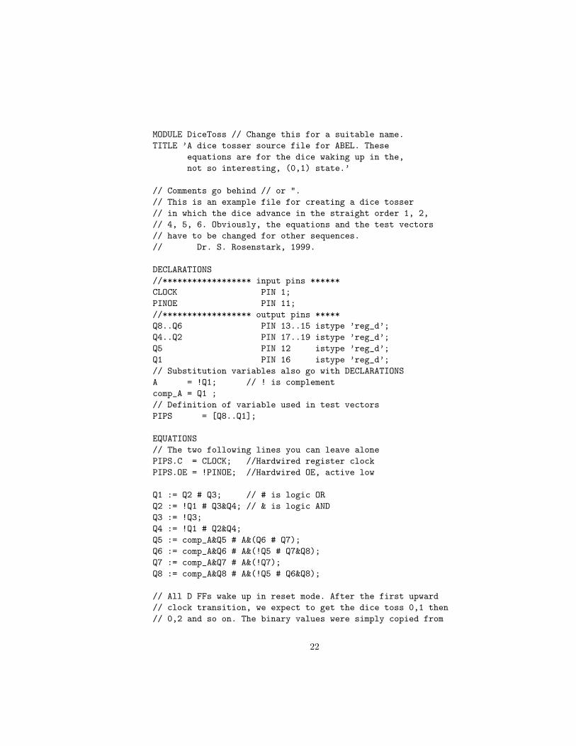
MODULE DiceToss // Change this for a suitable name.TITLE ’A dice tosser source file for ABEL. These
equations are for the dice waking up in the,not so interesting, (0,1) state.’
// Comments go behind // or ".// This is an example file for creating a dice tosser// in which the dice advance in the straight order 1, 2,// 4, 5, 6. Obviously, the equations and the test vectors// have to be changed for other sequences.// Dr. S. Rosenstark, 1999.
DECLARATIONS//****************** input pins ******CLOCK PIN 1;PINOE PIN 11;//****************** output pins *****Q8..Q6 PIN 13..15 istype ’reg_d’;Q4..Q2 PIN 17..19 istype ’reg_d’;Q5 PIN 12 istype ’reg_d’;Q1 PIN 16 istype ’reg_d’;// Substitution variables also go with DECLARATIONSA = !Q1; // ! is complementcomp_A = Q1 ;// Definition of variable used in test vectorsPIPS = [Q8..Q1];
EQUATIONS// The two following lines you can leave alonePIPS.C = CLOCK; //Hardwired register clockPIPS.OE = !PINOE; //Hardwired OE, active low
Q1 := Q2 # Q3; // # is logic ORQ2 := !Q1 # Q3&Q4; // & is logic ANDQ3 := !Q3;Q4 := !Q1 # Q2&Q4;Q5 := comp_A&Q5 # A&(Q6 # Q7);Q6 := comp_A&Q6 # A&(!Q5 # Q7&Q8);Q7 := comp_A&Q7 # A&(!Q7);Q8 := comp_A&Q8 # A&(!Q5 # Q6&Q8);
// All D FFs wake up in reset mode. After the first upward// clock transition, we expect to get the dice toss 0,1 then// 0,2 and so on. The binary values were simply copied from
22
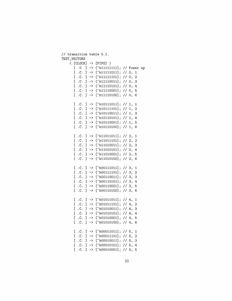
// transition table 5.1.TEST_VECTORS
( [CLOCK] -> [PIPS] )[ 0 ] -> [^b11111111]; // Power up[ .C. ] -> [^b11111011]; // 0, 1[ .C. ] -> [^b11111101]; // 0, 2[ .C. ] -> [^b11110011]; // 0, 3[ .C. ] -> [^b11110101]; // 0, 4[ .C. ] -> [^b11110001]; // 0, 5[ .C. ] -> [^b11110100]; // 0, 6
[ .C. ] -> [^b10111011]; // 1, 1[ .C. ] -> [^b10111101]; // 1, 2[ .C. ] -> [^b10110011]; // 1, 3[ .C. ] -> [^b10110101]; // 1, 4[ .C. ] -> [^b10110001]; // 1, 5[ .C. ] -> [^b10110100]; // 1, 6
[ .C. ] -> [^b11011011]; // 2, 1[ .C. ] -> [^b11011101]; // 2, 2[ .C. ] -> [^b11010011]; // 2, 3[ .C. ] -> [^b11010101]; // 2, 4[ .C. ] -> [^b11010001]; // 2, 5[ .C. ] -> [^b11010100]; // 2, 6
[ .C. ] -> [^b00111011]; // 3, 1[ .C. ] -> [^b00111101]; // 3, 2[ .C. ] -> [^b00110011]; // 3, 3[ .C. ] -> [^b00110101]; // 3, 4[ .C. ] -> [^b00110001]; // 3, 5[ .C. ] -> [^b00110100]; // 3, 6
[ .C. ] -> [^b01011011]; // 4, 1[ .C. ] -> [^b01011101]; // 4, 2[ .C. ] -> [^b01010011]; // 4, 3[ .C. ] -> [^b01010101]; // 4, 4[ .C. ] -> [^b01010001]; // 4, 5[ .C. ] -> [^b01010100]; // 4, 6
[ .C. ] -> [^b00011011]; // 5, 1[ .C. ] -> [^b00011101]; // 5, 2[ .C. ] -> [^b00010011]; // 5, 3[ .C. ] -> [^b00010101]; // 5, 4[ .C. ] -> [^b00010001]; // 5, 5
23
[ .C. ] -> [^b00010100]; // 5, 6
[ .C. ] -> [^b01001011]; // 6, 1[ .C. ] -> [^b01001101]; // 6, 2[ .C. ] -> [^b01000011]; // 6, 3[ .C. ] -> [^b01000101]; // 6, 4[ .C. ] -> [^b01000001]; // 6, 5[ .C. ] -> [^b01000100]; // 6, 6
END
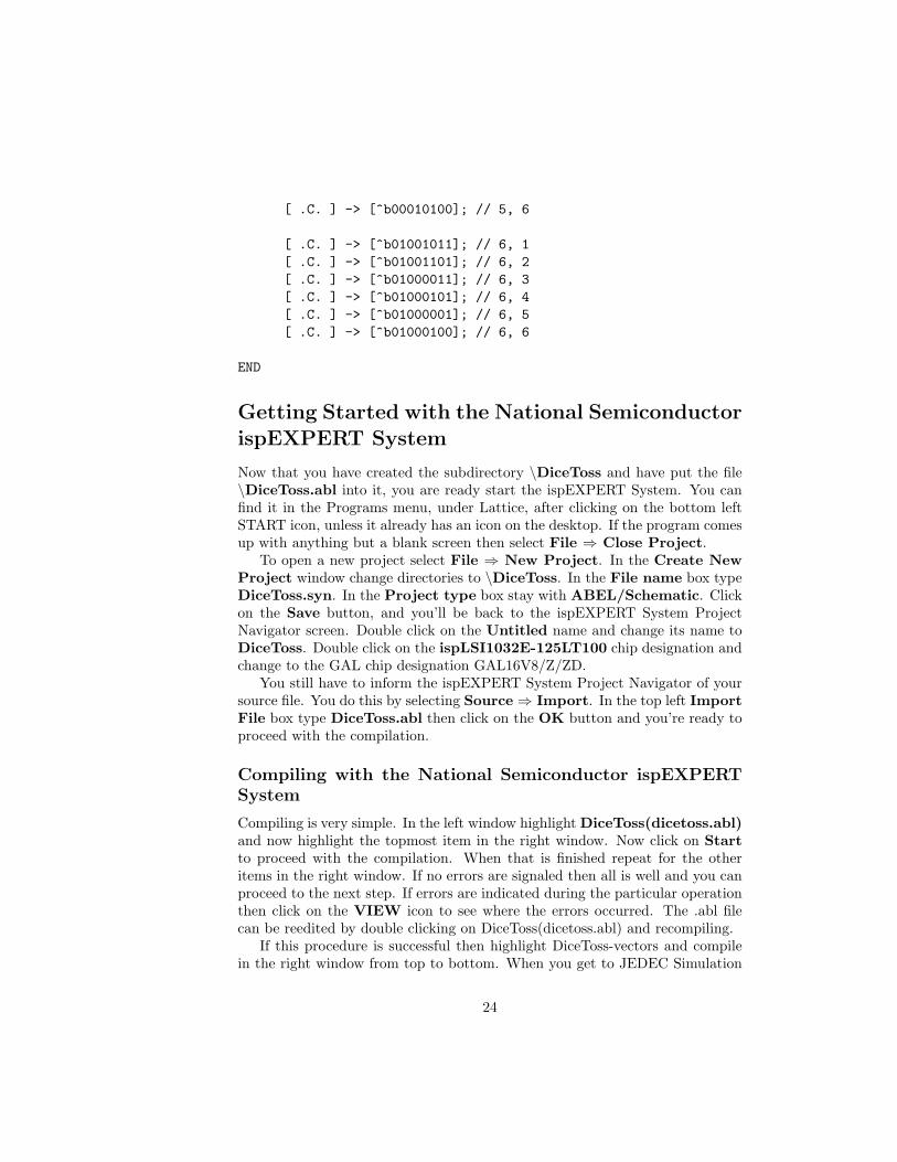
Getting Started with the National SemiconductorispEXPERT System
Now that you have created the subdirectory \DiceToss and have put the file\DiceToss.abl into it, you are ready start the ispEXPERT System. You canfind it in the Programs menu, under Lattice, after clicking on the bottom leftSTART icon, unless it already has an icon on the desktop. If the program comesup with anything but a blank screen then select File ⇒ Close Project.
To open a new project select File ⇒ New Project. In the Create NewProject window change directories to \DiceToss. In the File name box typeDiceToss.syn. In the Project type box stay with ABEL/Schematic. Clickon the Save button, and you’ll be back to the ispEXPERT System ProjectNavigator screen. Double click on the Untitled name and change its name toDiceToss. Double click on the ispLSI1032E-125LT100 chip designation andchange to the GAL chip designation GAL16V8/Z/ZD.
You still have to inform the ispEXPERT System Project Navigator of yoursource file. You do this by selecting Source ⇒ Import. In the top left ImportFile box type DiceToss.abl then click on the OK button and you’re ready toproceed with the compilation.
Compiling with the National Semiconductor ispEXPERTSystem
Compiling is very simple. In the left window highlight DiceToss(dicetoss.abl)and now highlight the topmost item in the right window. Now click on Startto proceed with the compilation. When that is finished repeat for the otheritems in the right window. If no errors are signaled then all is well and you canproceed to the next step. If errors are indicated during the particular operationthen click on the VIEW icon to see where the errors occurred. The .abl filecan be reedited by double clicking on DiceToss(dicetoss.abl) and recompiling.
If this procedure is successful then highlight DiceToss-vectors and compilein the right window from top to bottom. When you get to JEDEC Simulation
24

Waveform, you can view it by adding waveforms using the Edit, followed by theShow commands to add waveforms to your display. That way if your chip doesnot work properly you can look to see which waveform is incorrect and fromthis determine which equation needs to be corrected.
When all of the above steps are successful you’ll have the file DiceToss.jedin your subdirectory and you are ready to program your GAL. To do that,consult the section on Programming GALs and EEPROMs at the beginning ofthis manual.
If you are convinced that the .abl file has no errors at all then you can takea shortcut and simply highlight the GAL16V8/Z/ZD block in the left windowand then select the JEDEC File icon in the right window. Clicking on Startwill produce the JEDEC file.
The Implementation of the Dice Tosser Design
1. Having read the design example, students can now carry out the stepsneeded to successfully complete the design of their own dice tosser. Eachstudent will be given a unique dice sequence to implement.
2. Before the final implementation the student should pay attention to theresults of the compilation to become convinced that the design is correct.
3. After programming the GAL, the student can use the test jig to demon-strate to the class instructor that the device is indeed carrying out thesteps which it was designed to carry out.
4. The GAL wakes up with all D flip-flops set. This means that all Qn
outputs will be high, so no LEDs will light on the dice tosser. A singleclock pulse is generated so the dice immediately go to the (0,1) state.
A second part of the experiment is to modify the design to make thatthe dice tosser wakes up in the (1,1) state when power is applied to thetest jig. This is a good time to review the state table and get a betterunderstanding of the variable A. It is used to cause transitions in thesecond die.
The 16V8 GAL is being used in this laboratory to obtain performanceidentical to the 16R8 PAL. It should be readily apparent from the logicdiagram for the 16R8, that each equation can consist of the sum of nomore than 8 product terms. If in your redesign one of your equationsends up with the sum of more than 8 terms, then it is possible you didnot take proper care of the “don’t care” terms in you design. If you areconvinced that you did everything right, then speak to your instructor. Ifthe instructor is convinced that your dice sequence cannot be redesigned tostart with the (1,1) state, you may get permission to change the sequencecyclically. A cyclic shift moves all the numbers around in a circle by one
25
state, or if need be, by more than one state. For example 1, 2, 3, 4, 5, 6becomes 2, 3, 4, 5, 6, 1 after one shift or 3, 4, 5, 6, 1, 2 after two shifts.
5. Write the laboratory report in the same style as this text was written. Itshould describe each step in the design procedure. It can include a critiqueof this design, with suggestions for its improvement.
Appendix: Program for Selecting Random DiceFace Sequences
The instructor can use this program for generating dice sequences for the stu-dents. If you come up with a better program do let us know.
’Program to produce state order (dice face order) for implementation’by student in the Dice Tosser experiment. The current date can be’used as a random number generator seed.
INPUT "Any 6 digit number such as todays’s date ", DATERANDOMIZE (DATE) ’Current date used as a seedOPEN "dice.out" FOR OUTPUT AS #1
PRINT #1,PRINT #1, "Student # Dice Face Order"FOR J = 1 TO 40 ’Adjust for the number of students. Check
’output file DICE.OUT for duplicate sequences.
FOR I = 1 TO 6p(I) = 0 ’Start with dice face sequence nulled
NEXT I
y = 0 ’Dice face counter
DO UNTIL y = 6x1 = RND ’Get a random numberx = 6 * x1 + 1 ’Scale it to lie between 1 and 7x% = INT(x) ’Truncate the numberx5 = (x% = p(1) OR x% = p(2) OR x% = p(3))x6 = (x% = p(4) OR x% = p(5) OR x% = p(6))’Make sure you don’t store duplicate numbers
IF NOT (x5 OR x6) THEN y = y + 1: p(y) = x%LOOP
’Sort the numbers to lead with unity.
26
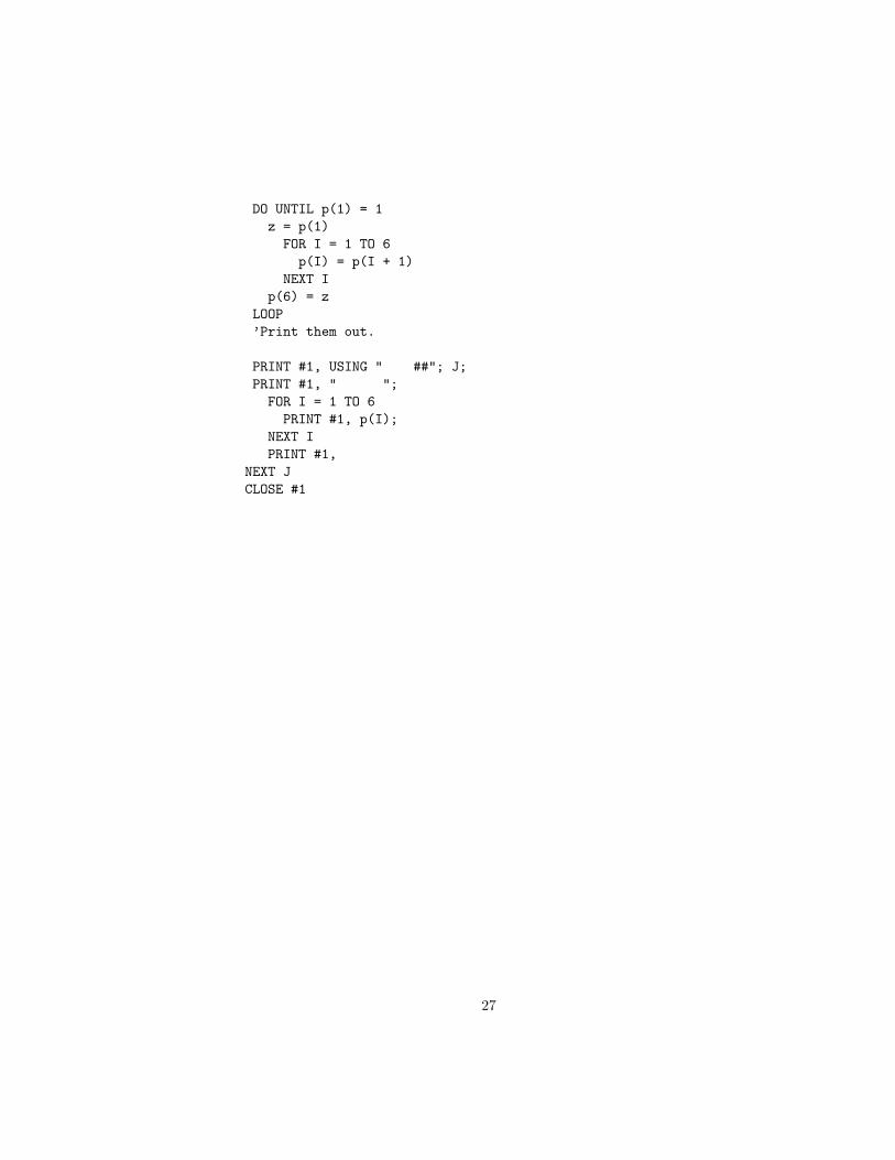
DO UNTIL p(1) = 1z = p(1)
FOR I = 1 TO 6p(I) = p(I + 1)
NEXT Ip(6) = z
LOOP’Print them out.
PRINT #1, USING " ##"; J;PRINT #1, " ";
FOR I = 1 TO 6PRINT #1, p(I);
NEXT IPRINT #1,
NEXT JCLOSE #1
27
EXPERIMENT 6: EventDriven Circuit
Objectives
The objective of this lab is to familiarize the student with design techniques forevent driven sequential circuits, and to introduce the student to applicationsinvolving ROMs.
Preparation
Review chapters 4 through 6 of Logic and Computer Design Fundamentals, byM. Morris Mano and Charles R. Kime, Prentice Hall, 1997.
Requisite Equipment
• Pencilbox kit
• One 2816A EEPROM
• One 74374 octal D-type latch (or CMOS equivalent).
• One debounced push button switch to simulate the system clock
• One DIP switch for simulating the inputs
• Three LEDs with current limiting resistors
References
• Logic and Computer Design Fundamentals, by M. Morris Mano and CharlesR. Kime, Prentice Hall, 1997.
28
Background
Introduction
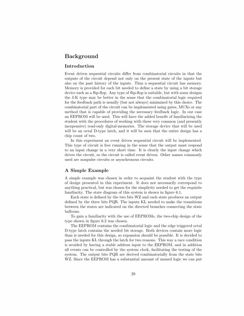
Event driven sequential circuits differ from combinatorial circuits in that theoutputs of the circuit depend not only on the present state of the inputs butalso on the past history of the inputs. Thus a sequential circuit has memory.Memory is provided for each bit needed to define a state by using a bit storagedevice such as a flip-flop. Any type of flip-flop is suitable, but with some designsthe J-K type may be better in the sense that the combinatorial logic requiredfor the feedback path is usually (but not always) minimized by this choice. Thecombinatorial part of the circuit can be implemented using gates, MUXs or anymethod that is capable of providing the necessary feedback logic. In our casean EEPROM will be used. This will have the added benefit of familiarizing thestudent with the procedures of working with these very common (and presentlyinexpensive) read-only digital-memories. The storage device that will be usedwill be an octal D-type latch, and it will be seen that the entire design has achip count of two.
In this experiment an event driven sequential circuit will be implemented.This type of circuit is free running in the sense that the output must respondto an input change in a very short time. It is clearly the input change whichdrives the circuit, so the circuit is called event driven. Other names commonlyused are nonpulse circuits or asynchronous circuits.
A Simple Example
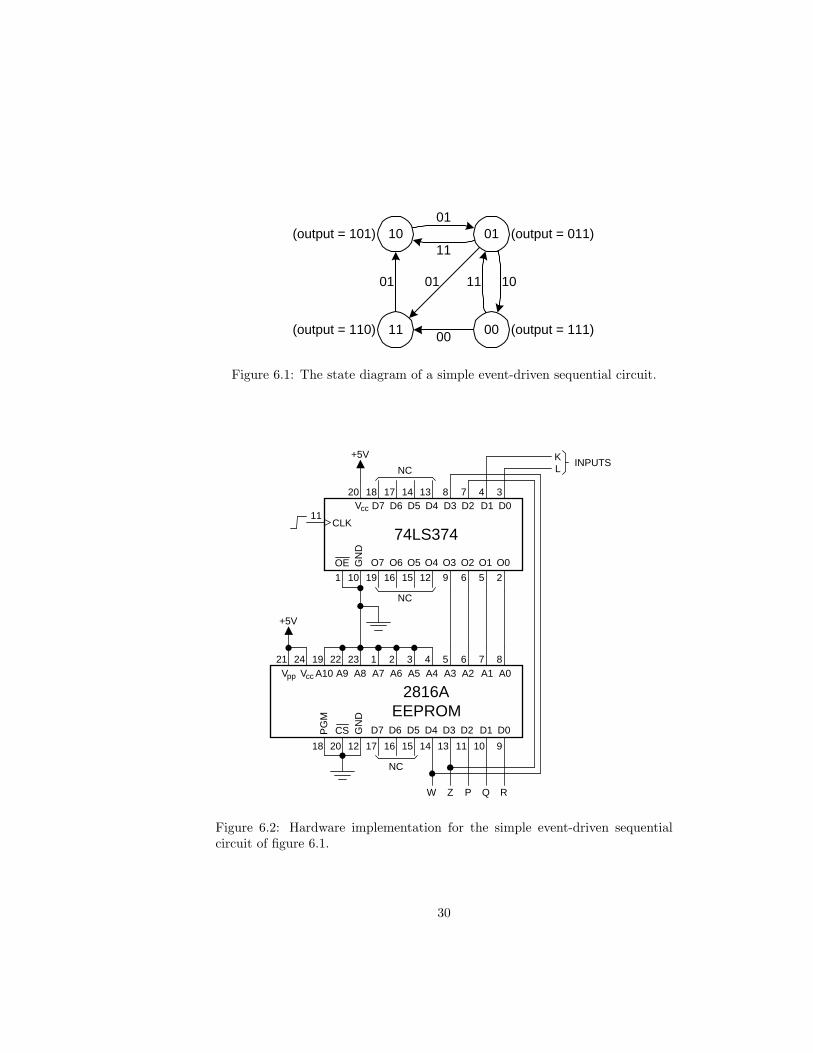
A simple example was chosen in order to acquaint the student with the typeof design presented in this experiment. It does not necessarily correspond toanything practical, but was chosen for the simplicity needed to get the requisitefamiliarity. The state diagram of this system is shown in figure 6.1.
Each state is defined by the two bits WZ and each state produces an outputdefined by the three bits PQR. The inputs KL needed to make the transitionsbetween the states are indicated on the directed branches connecting the stateballoons.
To gain a familiarity with the use of EEPROMs, the two-chip design of thetype shown in figure 6.2 was chosen.
The EEPROM contains the combinatorial logic and the edge triggered octalD-type latch contains the needed bit storage. Both devices contain more logicthan is needed for this design, so expansion should be possible. It is decided topass the inputs KL through the latch for two reasons. This way a race conditionis avoided by having a stable address input to the EEPROM, and in additionall events can be controlled by the system clock, facilitating the testing of thesystem. The output bits PQR are derived combinatorially from the state bitsWZ. Since the EEPROM has a substantial amount of unused logic we can put
29
10 01
11 00
01
11
11 10
00
01 01
(output = 101)
(output = 110)
(output = 011)
(output = 111)
Figure 6.1: The state diagram of a simple event-driven sequential circuit.G
ND
D0
74LS374 CLK
OE
11 V cc
20 18 17 14 13 8 7 4 3 D1 D2 D3 D4 D5 D6 D7
10 19 16 15 12 9 6 5 2 1
O0 O1 O2 O3 O4 O5 O6 O7
GN
D
A0
2816A EEPROM
PG
M
CS
22 V cc
5 6 7 8 A1 A2 A3 A4 A5 A6 A7
12 17 16 15 14 13 11 10 9
24 19 A8 A9 A10
D0 D1 D2 D3 D4 D5 D6 D7
1 2 3 4 23 V pp
21
18
+5V
+5V
NC
NC
W Z P Q R
NC
K L
INPUTS
20
Figure 6.2: Hardware implementation for the simple event-driven sequentialcircuit of figure 6.1.
30
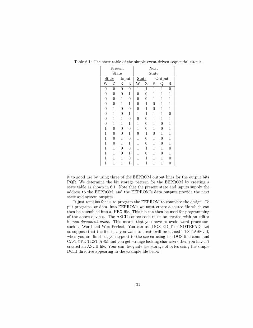
Table 6.1: The state table of the simple event-driven sequential circuit.
Present NextState State
State Input State OutputW Z K L W Z P Q R0 0 0 0 1 1 1 1 00 0 0 1 0 0 1 1 10 0 1 0 0 0 1 1 10 0 1 1 0 1 0 1 10 1 0 0 0 1 0 1 10 1 0 1 1 1 1 1 00 1 1 0 0 0 1 1 10 1 1 1 1 0 1 0 11 0 0 0 1 0 1 0 11 0 0 1 0 1 0 1 11 0 1 0 1 0 1 0 11 0 1 1 1 0 1 0 11 1 0 0 1 1 1 1 01 1 0 1 1 0 1 0 11 1 1 0 1 1 1 1 01 1 1 1 1 1 1 1 0
it to good use by using three of the EEPROM output lines for the output bitsPQR. We determine the bit storage pattern for the EEPROM by creating astate table as shown in 6.1. Note that the present state and inputs supply theaddress to the EEPROM, and the EEPROM’s data outputs provide the nextstate and system outputs.
It just remains for us to program the EEPROM to complete the design. Toput programs, or data, into EEPROMs we must create a source file which canthen be assembled into a .HEX file. This file can then be used for programmingof the above devices. The ASCII source code must be created with an editorin non-document mode. This means that you have to avoid word processorssuch as Word and WordPerfect. You can use DOS EDIT or NOTEPAD. Letus suppose that the file that you want to create will be named TEST.ASM. If,when you are finished, you type it to the screen using the DOS line commandC:>TYPE TEST.ASM and you get strange looking characters then you haven’tcreated an ASCII file. Your can designate the storage of bytes using the simpleDC.B directive appearing in the example file below.
31

ORG 0DC.B $41,$A3,$3F,$29,$5B,$7D,$09,$64
; As many lines similar to the above as neededEND
Your file will be small because you will be using only a small part of theEEPROM memory. The bits stored in the rest of the EEPROM are irrelevant,and the EEPROM programmer program will make some assumption about themand then go about its business. Once the source file is edited it can be assembledusing Antonakos’s assembler ASM68K which can be found in the subdirectory\ASM68K. You must be operating in DOS. If you are logged to the A drivethen, to assemble, simply type:
C:\ASM68K\ASM68K TEST<ENT>
When the assembly is finished you will have a MOTOROLA S-type of HEXfile TEST.HEX, as discussed in the Microprocessor Course. This can then beused to program the EEPROM using the programming instructions providedin the beginning of this manual under the title Programming GALs andEEPROMs. If errors are signaled then look at your TEST.LST file to find outwhat went wrong.
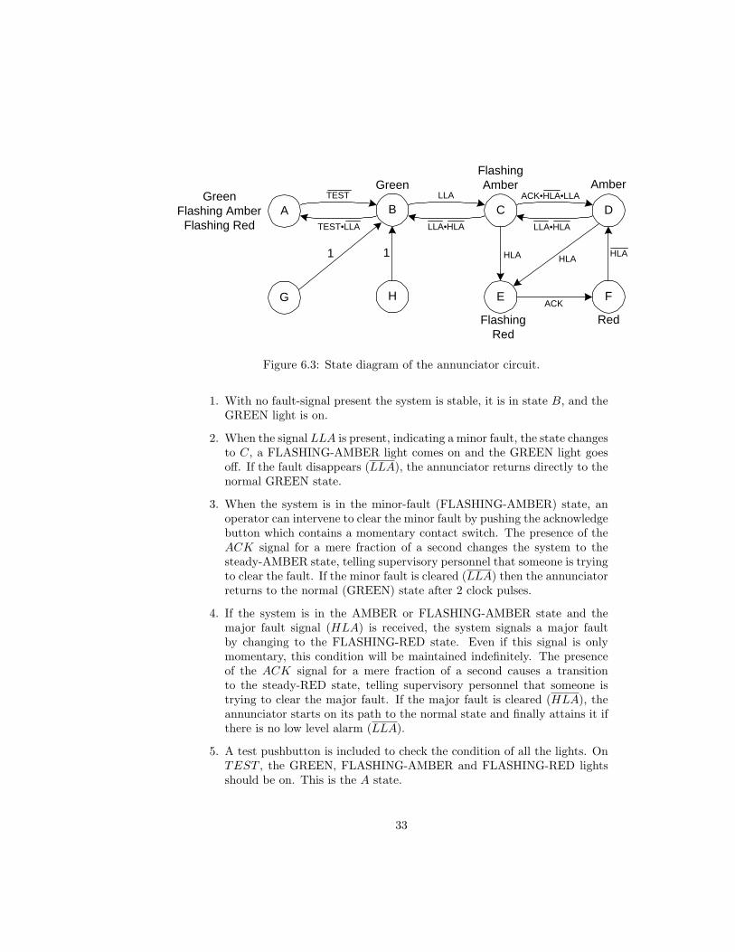
An Event Driven Annunciator System
The state diagram for the sequential circuit that we wish to design is shown infigure 6.3. It is a two alarm system which might be used in a factory to signalthat various levels of faults are occurring on the production line. One applicationmay be in process control, where the fault could indicate a high pressure. Aflashing amber light would indicate the first stage of pressure change, a potentialhazard. A large change in the system, shown by a flashing red light wouldindicate an emergency condition.
The annunciator has 6 proper states, so we will need a 3 bit sequentialcircuit. Each state is described by the 3 bits UVW. The annunciator monitorsthe factory for the presence of a low level alarm signal LLA and a high levelalarm signal HLA. The high level alarm signal HLA cannot occur if the lowlevel alarm signal LLA has not occurred first. The state diagram has the stateslabeled A through F . The instructor will assign the binary code of each stateto every student.
The operation of the circuit is best described by the state diagram of figure6.3. The circuit operates in the following manner:
32
A B
G H
1 1
F
TEST
HLA
Green Amber Green
Flashing Amber Flashing Red
Red
C
ACK E
HLA
Flashing Amber
Flashing Red
LLA
D ACK•HLA•LLA
LLA•HLA LLA•HLA TEST•LLA
HLA
Figure 6.3: State diagram of the annunciator circuit.
1. With no fault-signal present the system is stable, it is in state B, and theGREEN light is on.
2. When the signal LLA is present, indicating a minor fault, the state changesto C, a FLASHING-AMBER light comes on and the GREEN light goesoff. If the fault disappears (LLA), the annunciator returns directly to thenormal GREEN state.
3. When the system is in the minor-fault (FLASHING-AMBER) state, anoperator can intervene to clear the minor fault by pushing the acknowledgebutton which contains a momentary contact switch. The presence of theACK signal for a mere fraction of a second changes the system to thesteady-AMBER state, telling supervisory personnel that someone is tryingto clear the fault. If the minor fault is cleared (LLA) then the annunciatorreturns to the normal (GREEN) state after 2 clock pulses.
4. If the system is in the AMBER or FLASHING-AMBER state and themajor fault signal (HLA) is received, the system signals a major faultby changing to the FLASHING-RED state. Even if this signal is onlymomentary, this condition will be maintained indefinitely. The presenceof the ACK signal for a mere fraction of a second causes a transitionto the steady-RED state, telling supervisory personnel that someone istrying to clear the major fault. If the major fault is cleared (HLA), theannunciator starts on its path to the normal state and finally attains it ifthere is no low level alarm (LLA).
5. A test pushbutton is included to check the condition of all the lights. OnTEST , the GREEN, FLASHING-AMBER and FLASHING-RED lightsshould be on. This is the A state.
33

The Experiment
1. All the students should obtain their own unique 3-bit designation for thestates ABCDEFGH from the class instructor.
2. Having read the design example the student can now carry out the stepsneeded to successfully complete the design of the event driven annunciatorsystem. Each student is responsible for prototyping the design for testingpurposes.
3. Demonstrate to the class instructor that the device implements the designspecification.
34
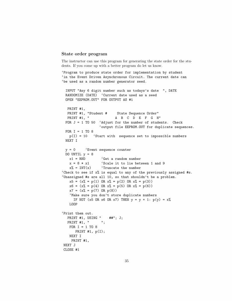
State order program
The instructor can use this program for generating the state order for the stu-dents. If you come up with a better program do let us know.
‘Program to produce state order for implementation by student‘in the Event Driven Asynchronous Circuit. The current date can‘be used as a random number generator seed.
INPUT "Any 6 digit number such as todays’s date ", DATERANDOMIZE (DATE) ‘Current date used as a seedOPEN "EEPROM.OUT" FOR OUTPUT AS #1
PRINT #1,PRINT #1, "Student # State Sequence Order"PRINT #1, " A B C D E F G H"
FOR J = 1 TO 50 ‘Adjust for the number of students. Check‘output file EEPROM.OUT for duplicate sequences.
FOR I = 1 TO 8p(I) = 10 ‘Start with sequence set to impossible numbers
NEXT I
y = 0 ‘Event sequence counterDO UNTIL y = 8
x1 = RND ‘Get a random numberx = 8 * x1 ‘Scale it to lie between 1 and 9x% = INT(x) ‘Truncate the number
‘Check to see if x% is equal to any of the previously assigned #s.‘Unassigned #s are all 10, so that shouldn’t be a problem.
x5 = (x% = p(1) OR x% = p(2) OR x% = p(3))x6 = (x% = p(4) OR x% = p(5) OR x% = p(6))x7 = (x% = p(7) OR p(8))‘Make sure you don’t store duplicate numbers
IF NOT (x5 OR x6 OR x7) THEN y = y + 1: p(y) = x%LOOP
‘Print them out.PRINT #1, USING " ##"; J;PRINT #1, " ";FOR I = 1 TO 8
PRINT #1, p(I);NEXT IPRINT #1,
NEXT JCLOSE #1
35
EXPERIMENT 7:Microsequencer Design
Objectives
To learn the basic operating principles of microsequencers.
Preparation
Review Chapter 7 of Computer Systems Organization and Architecture, by JohnD. Carpinelli, Addison Wesley, 2001.
Equipment needed
• Pencilbox kit
• One 2816A EEPROM
• One 74298 quad 2-to-1 multiplexer with latched outputs
• One debounced push button switch to simulate the system clock
• Two DIP switches
• Three LEDs and limiting resistors
• Additional 74-series ICs based on the student’s design
References
• Any textbook used in the prerequisite computer systems architecturecourse.
36
Background
Microsequencers
The control unit is responsible for coordinating actions within the CPU. Thecontrol unit decodes the instruction and issues a set of control signals that resultin the instruction’s execution. These control signals cause data to be routedcorrectly within the CPU, generate correct external control signals, such as RDand WR in the 8085, and cause the ALU to perform the correct operation onits data.
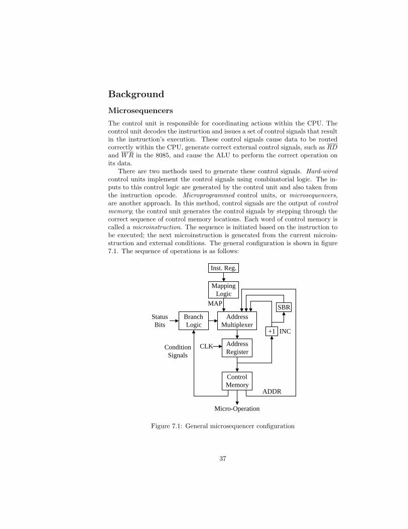
There are two methods used to generate these control signals. Hard-wiredcontrol units implement the control signals using combinatorial logic. The in-puts to this control logic are generated by the control unit and also taken fromthe instruction opcode. Microprogrammed control units, or microsequencers,are another approach. In this method, control signals are the output of controlmemory; the control unit generates the control signals by stepping through thecorrect sequence of control memory locations. Each word of control memory iscalled a microinstruction. The sequence is initiated based on the instruction tobe executed; the next microinstruction is generated from the current microin-struction and external conditions. The general configuration is shown in figure7.1. The sequence of operations is as follows:
Inst. Reg.
Mapping Logic
Address Multiplexer
Branch Logic
Status Bits
Address Register
+1
SBR
Control Memory
Micro-Operation
Condition Signals
MAP
CLK
INC
ADDR
Figure 7.1: General microsequencer configuration
37
1. The address of the next microinstruction to be executed is loaded into theaddress register. This becomes the input address to the control memory.
2. The control memory decodes its input address and puts out the microin-struction. This microinstruction has two functions. First, it makes avail-able the control signals to sequence execution of the instruction. Notethat the microsequencer does not actually execute the instruction; it gen-erates control signals which cause other hardware within the CPU (suchas the ALU) to execute the instruction. Second, it generates address andcondition signals.
3. Based on the condition signals, the multiplexer generates the address ofthe next microinstruction. Possible next addresses are discussed later inthis experiment.
Address multiplexer and mapping logic
The address multiplexer is used to select one out of a number of possible ad-dresses for the next microinstruction to be executed. There are four standardpossibilities.
INCR The next address in control memory. This is often used to execute aseries of microinstructions that occupy consecutive locations in controlmemory.
ADDR The address specified by control memory. This is used to specify jumpswithin control memory. This is typically used to jump to the opcode fetchroutine when finished executing the instruction. It is also combined withINCR to perform conditional jumps within the microcode, i.e. if the jumpis taken, the next microinstruction address is taken from ADDR, otherwiseit is taken from INCR.
SBR The address stored in the microsubroutine register. Just as high-level andassembly language programs may have subroutines which can be invokedfrom different locations within the program, microcode may also use mi-crosubroutines. These microsubroutines usually perform functions, suchas indirect addressing, that are common to many instructions. The mi-crosubroutine register contains the return address of the microsubroutine.The register is loaded when a microcall is executed and is read when amicroreturn is reached. If nested microsubroutines are used in the system,the register must be replaced with a hardware stack.
MAP The address based on the instruction to be executed. The mappinglogic reads the opcode of the instruction to be executed and generatesthe microaddress of the first microinstruction used to execute the instruc-tion. The logic used to generate the output depends on the placement ofmicrocode within the control memory.
38
The address to be used is determined by the branch logic. This is combina-torial logic that selects the next address based on the current microinstructionand external status bits. The branch logic also generates the signal used to loadSBR.
In this experiment, INCR and SBR are not used; only ADDR and MAPcan supply the next microaddress. Furthermore, all branches are unconditional,so the branch logic defaults to a single control signal derived from the controlmemory.
Microaddress register
This is a single register which holds the address of the microinstruction. Theclock used to load the register is actually the system clock.
In this experiment, the register is incorporated within the multiplexer chip.Instead of the oscillator normally used as the system clock, you will use a DE-BOUNCED push button switch to allow you to single step through the mi-crocode.
Control memory
The control memory is typically a small ROM. For this experiment, you willuse a 2816A EEPROM. You will enter the microcode using the DB assemblerdirective. Ground all unused address lines.
Other hardware
For this experiment, two additional pieces of hardware are needed. The instruc-tion register, which normally holds the opcode for input to the mapping logic,will be replaced by two DIP switches. This is done to simplify hardware andfacilitate debugging. Also, three LEDs with current-limiting resistors will beconnected to signals Z1, Z2 and Z3 of the control memory. Since this experi-ment does not actually use the other components of the CPU, the LEDs willbe used to monitor the control signals. Note that all LEDs must be driven byactive low logic.
Control memory format
All eight outputs of the control memory are used in this experiment. The formatis as follows.
39
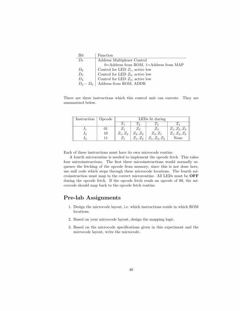
Bit FunctionD7 Address Multiplexer Control
0=Address from ROM, 1=Address from MAPD6 Control for LED Z1, active lowD5 Control for LED Z2, active lowD4 Control for LED Z3, active lowD3 −D0 Address from ROM, ADDR
There are three instructions which this control unit can execute. They aresummarized below.
Instruction Opcode LEDs lit duringT1 T2 T3 T4
I1 01 Z1 Z2 Z3 Z1, Z2, Z3
I2 10 Z1, Z2 Z2, Z3 Z3, Z1 Z1, Z2, Z3
I3 11 Z1 Z1, Z2 Z1, Z2, Z3 None
Each of these instructions must have its own microcode routine.A fourth microroutine is needed to implement the opcode fetch. This takes
four microinstructions. The first three microinstructions would normally se-quence the fetching of the opcode from memory; since this is not done here,use null code which steps through these microcode locations. The fourth mi-croinstruction must map to the correct microroutine. All LEDs must be OFFduring the opcode fetch. If the opcode fetch reads an opcode of 00, the mi-crocode should map back to the opcode fetch routine.
Pre-lab Assignments
1. Design the microcode layout, i.e. which instructions reside in which ROMlocations.
2. Based on your microcode layout, design the mapping logic.
3. Based on the microcode specifications given in this experiment and themicrocode layout, write the microcode.
40

Experimental Procedure
1. Burn the microcode into the 2816A EEPROM.
2. Wire and test the circuit. Use the debounced push button switch for thesystem clock, and the toggle switches for the instruction register. Test thesystem and demonstrate it to the instructor.
41


![Chapter 458-61A Chapter 458-61A WAC REAL …lawfilesext.leg.wa.gov/law/WACArchive/2013/WAC-458-61A...458-61A-101 Real Estate Excise Tax [Ch. 458-61A WAC—p. 2] (8/3/11) Legislation](https://img.pdfslide.net/doc/110x75/5fb4b3e18aff3f19c748349f/chapter-458-61a-chapter-458-61a-wac-real-458-61a-101-real-estate-excise-tax.jpg)

![Title 458 Title 458 WAC REVENUE, DEPARTMENT OFleg.wa.gov/CodeReviser/WACArchive/Documents/2005/WAC458A.pdf · (2005 Ed.) [Title 458 WAC—p. 1] Title 458 Title 458 WAC REVENUE, DEPARTMENT](https://img.pdfslide.net/doc/110x75/5bfc3f4009d3f2bc6e8b6469/title-458-title-458-wac-revenue-department-oflegwagovcodereviserwacarchivedocuments2005.jpg)