Embed Size (px)
Citation preview
Version 1
Total pages 18 Date 2003.05.26
Product Specification10.2〞color TFT-LCD module
( ◆ ) Preliminary Specification ( ….. ) Final Specification
MODEL NAME: A102VW01
Note: The content o f th is spec i f ica t ion is sub jec t to change.
© 2002 AU Optronics All Rights Reserved, Do Not Copy.

Record of Revision Version Revise Date Page Content
1 26/May./2003 0 First draft.
Version : 1
Page : 1 /18
ALL RIGHTS STRICTLY RESERVED. ANY PORTION OF THIS PAPER SHALL NOT BE REPRODUCED, COPIED, OR TRANSFORMED TO ANY OTHER FORMS WITHOUT PERMISSION FROM UNIPAC OPTOELECTRONICS CORP.
Contents: A. Physical specification. . . . . . . . . . . . . . . . . . . . . . . . . . . . . . . . . . . . . . . . . . . . . . . . . . . . . P3
B. Electrical specifications. . . . . . . . . . . . . . . . . . . . . . . . . . . . . . . . . . . . . . . . . . . . . . . . . . . P4
1. Pin assignment. . . . . . . . . . . . . . . . . . . . . . . . . . . . . . . . . . . . . . . . . . . . . . . . . . . . . . . . . . . . P4
a.TFT-LCD panel driving section. . . . . . . . . . . . . . . . . . . . . . . . . . . . . . . . . . . . . . . . . . . P4
b.Backlight driving section. . . . . . . . . . . . . . . . . . . . . . . . . . . . . . . . . . . . . . . . . . . . . . . . . P5
2.Absolute maximum ratings. . . . . . . . . . . . . . . . . . . . . . . . . . . . . . . . . . . . . . . . . . . . . . . . . . P5
3. Electrical characteristics. . . . . . . . . . . . . . . . . . . . . . . . . . . . . . . . . . . . . . . . . . . . . . . . . . . . P6
a. Typical operating conditions. . . . . . . . . . . . . . . . . . . . . . . . . . . . . . . . . . . . . . . . . . . . . P6
b. Current consumption. . . . . . . . . . . . . . . . . . . . . . . . . . . . . . . . . . . . . . . . . . . . . . . . . . . . P6
c. Backlight driving conditions . . . . . . . . . . . . . . . . . . . . . . . . . . . . . . . . . . . . . . . . . P6
4. AC Timing. . . . . . . . . . . . . . . . . . . . . . . . . . . . . . . . . . . . . . . . . . . . . . . . . . . . . . . . . . . . . . . . . P7
a. Timing conditions. . . . . . . . . . . . . . . . . . . . . . . . . . . . . . . . . . . . . . . . . . . . . . . . . . . . . . . P7
b. Timing diagram. . . . . . . . . . . . . . . . . . . . . . . . . . . . . . . . . . . . . . . . . . . . . . . . . . . . . . . . . P7
C. Optical specifications. . . . . . . . . . . . . . . . . . . . . . . . . . . . . . . . . . . . . . . . . . . . . . . . . . . P8
D. Reliability test items. . . . . . . . . . . . . . . . . . . . . . . . . . . . . . . . . . . . . . . . . . . . . . . . . . . . . . . P10
E. Packing form. . . . . . . . . . . . . . . . . . . . . . . . . . . . . . . . . . . . . . . . . . . . . . . . . . . . . . . . . . . . . . . P11
Version : 1
Page : 2 /18
ALL RIGHTS STRICTLY RESERVED. ANY PORTION OF THIS PAPER SHALL NOT BE REPRODUCED, COPIED, OR TRANSFORMED TO ANY OTHER FORMS WITHOUT PERMISSION FROM UNIPAC OPTOELECTRONICS CORP.
Appendix: Fig.1 Outline dimension of TFT-LCD module (Front Side). . . . . . . . . . P12 Fig.2 Outline dimension of TFT-LCD module (Rear Side) P13 Fig.3 Operation Mode 1. . . . . . . . . . . . . . . . . . . . . . . . . . . . . . . . . . . . . . . . . . . . . . . . . . . . P14 Fig.4 Operation Mode 2 . . . . . . . . . . . . . . . . . . . . . . . . . . . . . . . . . . . . . . . . . . . . . . P15 Fig.5 Horizontal timing. . . . . . . . . . . . . . . . . . . . . . . . . . . . . . . . . . . . . . . . . . . . . . . . . . . . . P16 Fig.6 Vertical shift timing P17 Fig.7 Vertical timing (from up to down) P18
Version : 1
Page : 3 /18
ALL RIGHTS STRICTLY RESERVED. ANY PORTION OF THIS PAPER SHALL NOT BE REPRODUCED, COPIED, OR TRANSFORMED TO ANY OTHER FORMS WITHOUT PERMISSION FROM UNIPAC OPTOELECTRONICS CORP.
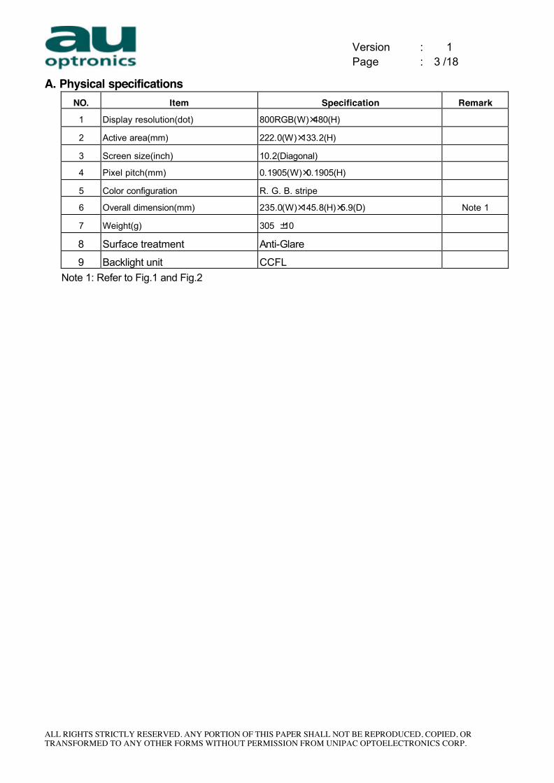
A. Physical specifications NO. Item Specification Remark
1 Display resolution(dot) 800RGB(W)×480(H)
2 Active area(mm) 222.0(W)×133.2(H)
3 Screen size(inch) 10.2(Diagonal)
4 Pixel pitch(mm) 0.1905(W)×0.1905(H)
5 Color configuration R. G. B. stripe
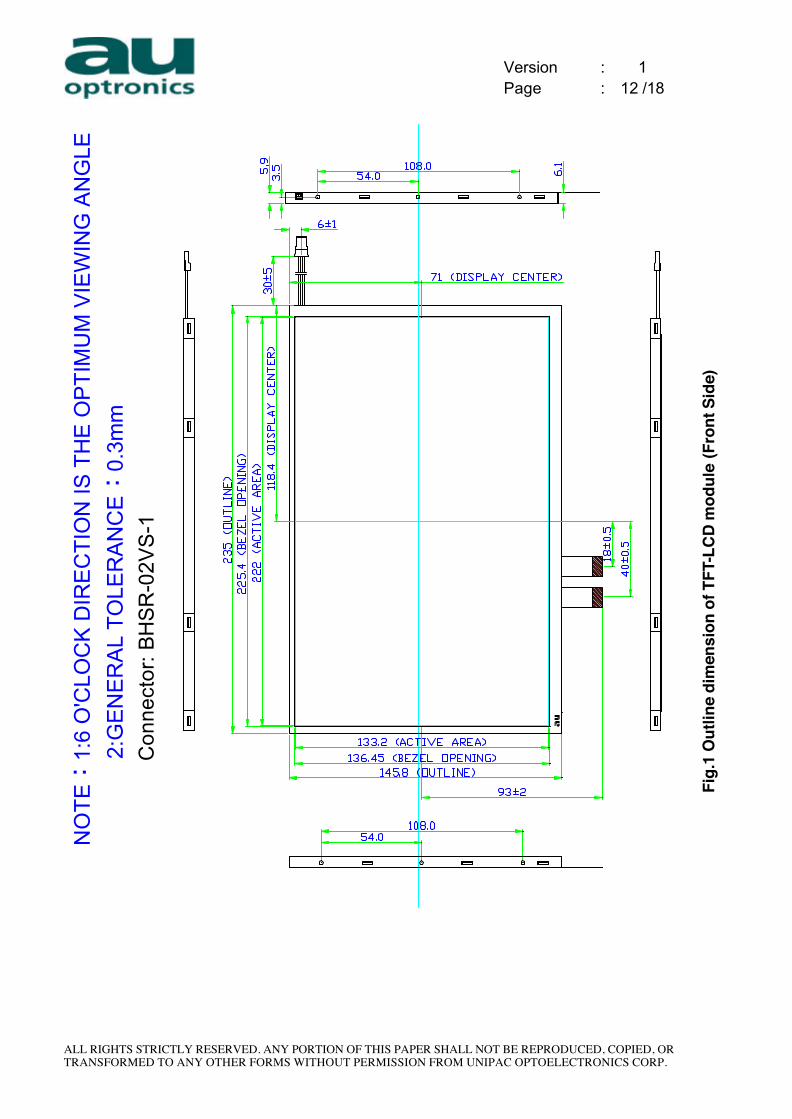
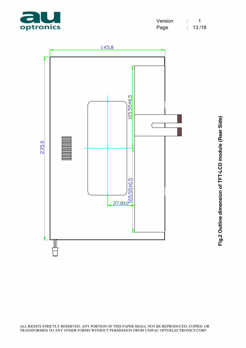
6 Overall dimension(mm) 235.0(W)×145.8(H)×5.9(D) Note 1
7 Weight(g) 305 ±10
8 Surface treatment Anti-Glare
9 Backlight unit CCFL Note 1: Refer to Fig.1 and Fig.2
Version : 1
Page : 4 /18
ALL RIGHTS STRICTLY RESERVED. ANY PORTION OF THIS PAPER SHALL NOT BE REPRODUCED, COPIED, OR TRANSFORMED TO ANY OTHER FORMS WITHOUT PERMISSION FROM UNIPAC OPTOELECTRONICS CORP.
B. Electrical specifications
1. Absolute Maximum Rat ings
Product Specification Items Symbol
Min. Typ. Max. Unit
Vcc -0.5 5 V AVDD -0.5 12 V VGH -0.3 18 V VGL -15 0.3 V
Power Voltage
VGH-VGL 33 V Vi -0.3 Vcc+0.3 V
Vref(V1~V8) 0.4AVDD AVDD+0.3 V
Vref(V8~V14) -0.3 0.6AVDD V Input Signal
Voltage
Vcom 4.2 V Operating
Temperature Topa -30 85 ℃
Storage Temperature Tstg -40 95 ℃
2. Typica l operat ing condi t ions (GND=AV S S =0V)
Product Specification Items Symbol
Min. Typ. Max. Unit
Vcc 3.0 3.3 3.6 V AVDD (7.8) (8.4) (9.0) V VGH 14.3 15 15.7 V
VCOM (4.2) V
Power Voltage
VGL -10.5 -10 -9.5 V V1~V5 0.4AVDD — AVDD-0.3 V Input
Reference Voltage V6~V10 0.1 — 0.6AVDD V
VIH 0.8VCC — VCC V Input H/L level
Voltage VIL 0 — 0.2VCC V
3. Current consumption conditions(GND=Avss=0V)
Parameter Symbol Condition Min. Typ. Max. Unit
IGH VGH=15V (50) (100) uA IGL VGL=-10V (-0.2) (-0.6) uA ICC VCC=5V (3.5) (5) mA
Current
For
Driver IDD AVDD=5V (20) (30) mA

Version : 1
Page : 5 /18
ALL RIGHTS STRICTLY RESERVED. ANY PORTION OF THIS PAPER SHALL NOT BE REPRODUCED, COPIED, OR TRANSFORMED TO ANY OTHER FORMS WITHOUT PERMISSION FROM UNIPAC OPTOELECTRONICS CORP.
4. Backlight driving conditions
Parameter Symbol Condition Min. Typ. Max. Unit Lamp Life
Time - - 25,000 40,000 - Hours
Voltage VL 610 660 Vrms Current IL 6.0 7.0 mA
Frequency FL 60 80 KHz T=25℃ 930 Vrms T=0℃ 1,220 Vrms
Lamp Start
Voltage Vs
T=-20℃ TBD Vrms The” Lamp life time” is defined as the module brightness decrease to 50% original brightness at Ta=25℃ , IL=6mA.
5. Timing conditions AC Electrical Characteristics (VCC=3.3V, AVDD=8.4V, AVSS=GND=0V, TA=25℃)
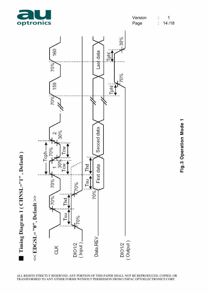
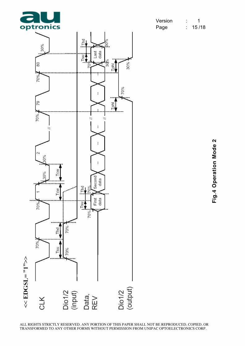
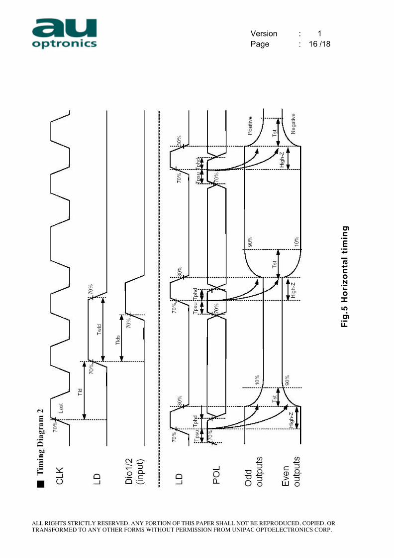
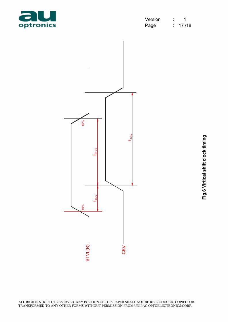
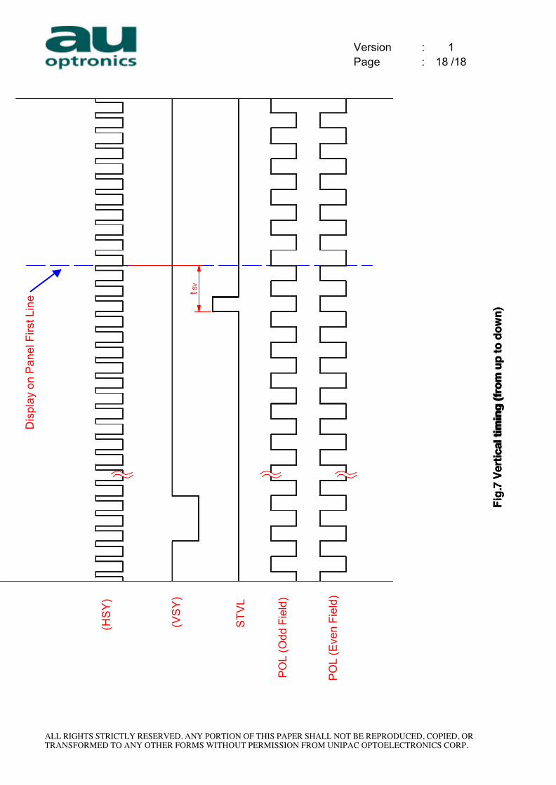
Parameter Symbol Min. Typ. Max. Unit CLK frequency Fclk 40 42 MHz CLK pulse width TCW 6 ns Data set-up time Tsu 4 ns Data hold time Thd 2 ns Propagation delay of DIO2/1 Tphl 6 10 15 ns Time that the last data to LD Tld 1 Tcw Pulse width of LD Twld 2 Tcw Time that LD to DIO1/2 Tlds 5 Tcw POL set-up time Tpsu 6 ns POL hold time Tphd 6 ns OEV pulse width TOEV 12 Tcw CKV pulse width TCKV 16 28 40 Tcw Horizontal display start TSH 0 Tcw/3 Horizontal display timing range TDH 800 Tcw/3 STV setup time TSUV 400 ns STV hold time THDV 400 ns STV pulse width TSTV 1 TDH Horizontal lines per field TV 512 525 610 TDH Vertical display start TSV 3 TDH Vertical display timing range TDV 480 TDH
DC Electrical Characteristics
Parameter Symbol Min. Typ. Max. Unit Supply Voltage Vcc 2.7 3.3 3.6 V Low Level Input Voltage Vil 0 - 0.3*Vcc V High Level Input Voltage Vih 0.7*Vcc - Vcc V High Level Output Voltage Voh Vcc-0.4 - - V Low Level Output Voltage Vol GND - GND+0.4 V Supply Voltage AVDD (6.5) (8.4) (10) V Sinking Current of Outputs IOL |-80| - - uA Driving Current of Outputs IOH 80 - - uA
Version : 1
Page : 6 /18
ALL RIGHTS STRICTLY RESERVED. ANY PORTION OF THIS PAPER SHALL NOT BE REPRODUCED, COPIED, OR TRANSFORMED TO ANY OTHER FORMS WITHOUT PERMISSION FROM UNIPAC OPTOELECTRONICS CORP.
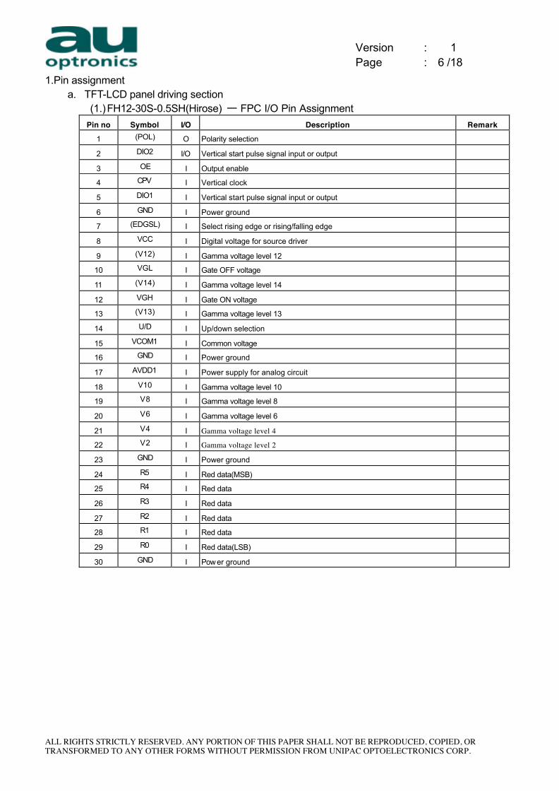
1.Pin assignment a. TFT-LCD panel driving section
(1.) FH12-30S-0.5SH(Hirose) — FPC I/O Pin Assignment Pin no Symbol I/O Description Remark
1 (POL) O Polarity selection
2 DIO2 I/O Vertical start pulse signal input or output
3 OE I Output enable
4 CPV I Vertical clock
5 DIO1 I Vertical start pulse signal input or output
6 GND I Power ground
7 (EDGSL) I Select rising edge or rising/falling edge
8 VCC I Digital voltage for source driver
9 (V12) I Gamma voltage level 12
10 VGL I Gate OFF voltage
11 (V14) I Gamma voltage level 14
12 VGH I Gate ON voltage
13 (V13) I Gamma voltage level 13
14 U/D I Up/down selection
15 VCOM1 I Common voltage
16 GND I Power ground
17 AVDD1 I Power supply for analog circuit
18 V10 I Gamma voltage level 10
19 V8 I Gamma voltage level 8
20 V6 I Gamma voltage level 6
21 V4 I Gamma voltage level 4
22 V2 I Gamma voltage level 2
23 GND I Power ground
24 R5 I Red data(MSB)
25 R4 I Red data
26 R3 I Red data
27 R2 I Red data
28 R1 I Red data
29 R0 I Red data(LSB)
30 GND I Pow er ground
Version : 1
Page : 7 /18
ALL RIGHTS STRICTLY RESERVED. ANY PORTION OF THIS PAPER SHALL NOT BE REPRODUCED, COPIED, OR TRANSFORMED TO ANY OTHER FORMS WITHOUT PERMISSION FROM UNIPAC OPTOELECTRONICS CORP.
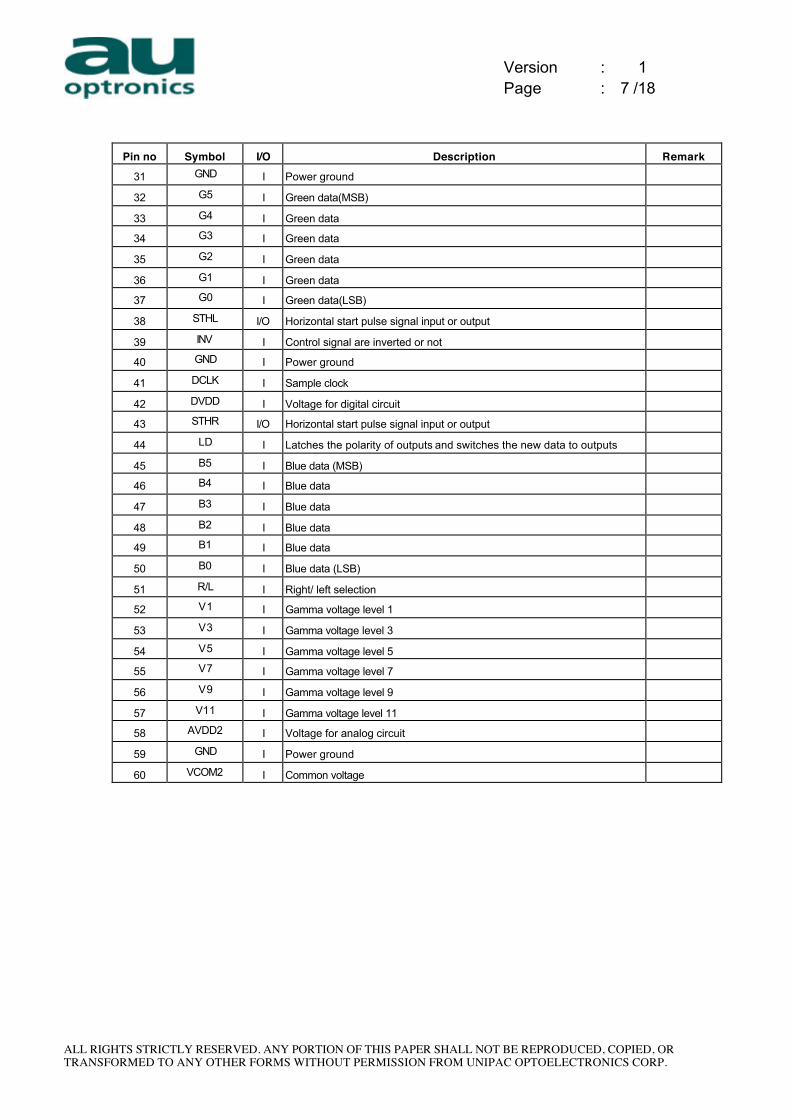
Pin no Symbol I/O Description Remark
31 GND I Power ground
32 G5 I Green data(MSB)
33 G4 I Green data
34 G3 I Green data
35 G2 I Green data
36 G1 I Green data
37 G0 I Green data(LSB)
38 STHL I/O Horizontal start pulse signal input or output
39 INV I Control signal are inverted or not
40 GND I Power ground
41 DCLK I Sample clock
42 DVDD I Voltage for digital circuit
43 STHR I/O Horizontal start pulse signal input or output
44 LD I Latches the polarity of outputs and switches the new data to outputs
45 B5 I Blue data (MSB)
46 B4 I Blue data
47 B3 I Blue data
48 B2 I Blue data
49 B1 I Blue data
50 B0 I Blue data (LSB)
51 R/L I Right/ left selection
52 V1 I Gamma voltage level 1
53 V3 I Gamma voltage level 3
54 V5 I Gamma voltage level 5
55 V7 I Gamma voltage level 7
56 V9 I Gamma voltage level 9
57 V11 I Gamma voltage level 11
58 AVDD2 I Voltage for analog circuit
59 GND I Power ground
60 VCOM2 I Common voltage
Version : 1
Page : 8 /18
ALL RIGHTS STRICTLY RESERVED. ANY PORTION OF THIS PAPER SHALL NOT BE REPRODUCED, COPIED, OR TRANSFORMED TO ANY OTHER FORMS WITHOUT PERMISSION FROM UNIPAC OPTOELECTRONICS CORP.
C. Optical specification (Note 1, Note 2) Item Symbol Condition Min. Typ. Max. Unit Remark
Response time Rise Fall
Tr Tf
θ=0∘ - -
12 18
24 36
ms ms
Note 3,5
Contrast ratio CR At optimized
Viewing angle
250 300 - Note 4, 5
Viewing angle
Top Bottom
Left Right
CR≧10
40 50 50 50
50 60 60 60
- - - -
deg.
Note 5, 6
Brightness YL IL=6mA, 25℃ 400 450 - nit Note 7
X θ=0∘ 0.26 0.31 0.36 White chromaticity
Y θ=0∘ 0.28 0.33 0.38
Note 7
Note 1 : Ambient temperature =25℃, and lamp current IL = 6 mArms. To be measured in the dark room. DC/AC inverter driving frequency: 60 kHz.
Note 2 :To be measured on the center area of panel with a viewing cone of 1∘by Topcon luminance meter BM-5, after 10 minutes operation.
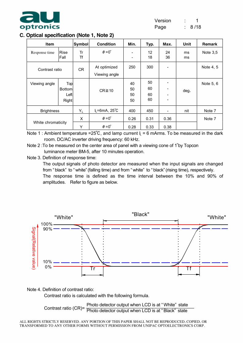
Note 3. Definition of response time: The output signals of photo detector are measured when the input signals are changed from “ black” to “ white” (falling time) and from “ white” to “ black” (rising time), respectively. The response time is defined as the time interval between the 10% and 90% of amplitudes. Refer to figure as below.
Note 4. Definition of contrast ratio: Contrast ratio is calculated with the following formula. Contrast ratio (CR)=
Signal(R
elative value)"Black"
Tr Tf
"White""White"
0%10%
90%100%
Photo detector output when LCD is at “ White” state Photo detector output when LCD is at “ Black” state
Version : 1
Page : 9 /18
ALL RIGHTS STRICTLY RESERVED. ANY PORTION OF THIS PAPER SHALL NOT BE REPRODUCED, COPIED, OR TRANSFORMED TO ANY OTHER FORMS WITHOUT PERMISSION FROM UNIPAC OPTOELECTRONICS CORP.
Note 5. White Vi=Vi50 + 1.5V Black Vi=Vi50 ± 2.0V “±” means that the analog input signal swings in phase with VCOM signal.
“ ” means that the analog input signal swings out of phase with VCOM signal. Vi50 : The analog input voltage when transmission is 50% The 100% transmission is defined as the transmission of LCD panel when all the input terminals of module are electrically opened.
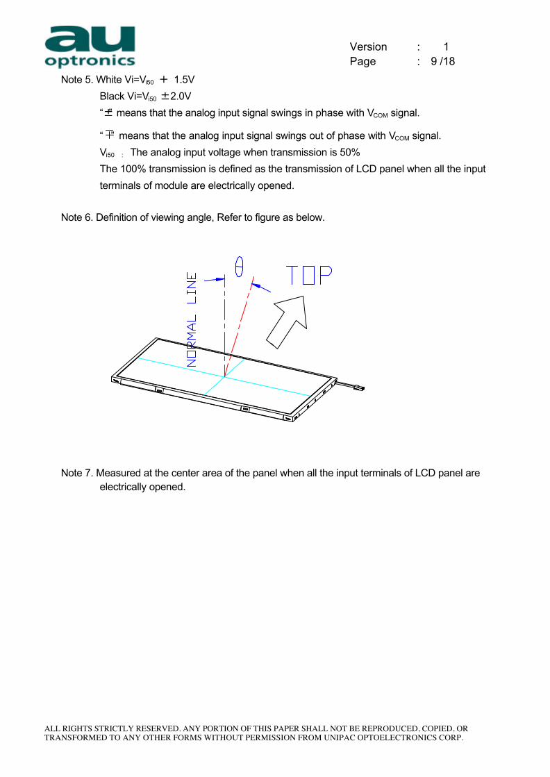
Note 6. Definition of viewing angle, Refer to figure as below.
Note 7. Measured at the center area of the panel when all the input terminals of LCD panel are
electrically opened.
Version : 1
Page : 10 /18
ALL RIGHTS STRICTLY RESERVED. ANY PORTION OF THIS PAPER SHALL NOT BE REPRODUCED, COPIED, OR TRANSFORMED TO ANY OTHER FORMS WITHOUT PERMISSION FROM UNIPAC OPTOELECTRONICS CORP.
D. Reliability test items(Note 2): No. Test items Conditions Remark
1 High temperature storage Ta= 85℃ 240Hrs
2 Low temperature storage Ta= -30℃ 240Hrs
3 High temperature operation Ta= 70℃ 240Hrs
4 Low temperature operation Ta= -20℃ 240Hrs
5 High temperature and high humidity Ta= 60℃, 90% RH 240Hrs Operation
6 Heat shock -30℃~85℃/100 cycles 1Hrs/cycle Non-operation
7 Electrostatic discharge ±200V,200pF(0Ω), once for each terminal
Non-operation
Frequency range : 8~33.3Hz
Stoke : 1.3mm Sweep : 2.9G, 33.3 ~ 400Hz Cycle : 15 minutes 2 hours for each direction of X,Z
8 Vibration
4 hours for Y direction
JIS C7021, A-10 condition A
9 Mechanical shock 100G, 6ms, ±X,±Y,±Z
3 times for each direction
JIS C7021, A-7 condition C
10 Vibration (with carton) Random vibration: 0.015G2/Hz from 5~200Hz –6dB/octave from 200~500Hz
IEC 68-34
11 Drop (with carton) Height: 60cm 1 corner, 3 edges, 6 surfaces
JIS Z0202
Note1: Ta: Ambient temperature. Note2: In the standard conditions, there is not display function NG issue occurred. All the
cosmetic specification is judged before the reliability stress.
Version : 1
Page : 11 /18
ALL RIGHTS STRICTLY RESERVED. ANY PORTION OF THIS PAPER SHALL NOT BE REPRODUCED, COPIED, OR TRANSFORMED TO ANY OTHER FORMS WITHOUT PERMISSION FROM UNIPAC OPTOELECTRONICS CORP.
E. Packing form TBD
Version : 1
Page : 12 /18
ALL RIGHTS STRICTLY RESERVED. ANY PORTION OF THIS PAPER SHALL NOT BE REPRODUCED, COPIED, OR TRANSFORMED TO ANY OTHER FORMS WITHOUT PERMISSION FROM UNIPAC OPTOELECTRONICS CORP.
2:
GE
NE
RA
L TO
LER
AN
CE:
0.3m
mN
OTE:
1:6
O'C
LOC
K D
IREC
TIO
N IS
TH
E O
PTIM
UM
VIE
WIN
G A
NG
LE
Fi
g.1
Out
line
dim
ensi
on o
f TFT
-LC
D m
odul
e (F
ront
Sid
e)
Con
nect
or: B
HSR
-02V
S-1
Version : 1
Page : 13 /18
ALL RIGHTS STRICTLY RESERVED. ANY PORTION OF THIS PAPER SHALL NOT BE REPRODUCED, COPIED, OR TRANSFORMED TO ANY OTHER FORMS WITHOUT PERMISSION FROM UNIPAC OPTOELECTRONICS CORP.
Fi
g.2
Out
line
dim
ensi
on o
f TFT
-LC
D m
odul
e (R
ear S
ide)
Version : 1
Page : 14 /18
ALL RIGHTS STRICTLY RESERVED. ANY PORTION OF THIS PAPER SHALL NOT BE REPRODUCED, COPIED, OR TRANSFORMED TO ANY OTHER FORMS WITHOUT PERMISSION FROM UNIPAC OPTOELECTRONICS CORP.
Fig.
3 O
pera
tion
Mod
e 1
Version : 1
Page : 15 /18
ALL RIGHTS STRICTLY RESERVED. ANY PORTION OF THIS PAPER SHALL NOT BE REPRODUCED, COPIED, OR TRANSFORMED TO ANY OTHER FORMS WITHOUT PERMISSION FROM UNIPAC OPTOELECTRONICS CORP.
Fig.
4 O
pera
tion
Mod
e 2
Version : 1
Page : 16 /18
ALL RIGHTS STRICTLY RESERVED. ANY PORTION OF THIS PAPER SHALL NOT BE REPRODUCED, COPIED, OR TRANSFORMED TO ANY OTHER FORMS WITHOUT PERMISSION FROM UNIPAC OPTOELECTRONICS CORP.
Fig.
5 H
oriz
onta
l tim
ing
Version : 1
Page : 17 /18
ALL RIGHTS STRICTLY RESERVED. ANY PORTION OF THIS PAPER SHALL NOT BE REPRODUCED, COPIED, OR TRANSFORMED TO ANY OTHER FORMS WITHOUT PERMISSION FROM UNIPAC OPTOELECTRONICS CORP.
STV
L(R
)
CK
V
50%
50%
t SU
VH
DV
t
t CKV
Fi
g.6
Virti
cal s
hift
cloc
k tim
ing
Version : 1
Page : 18 /18
ALL RIGHTS STRICTLY RESERVED. ANY PORTION OF THIS PAPER SHALL NOT BE REPRODUCED, COPIED, OR TRANSFORMED TO ANY OTHER FORMS WITHOUT PERMISSION FROM UNIPAC OPTOELECTRONICS CORP.
(VS
Y)
(HSY
)
tSV
Fig.
7 Ve
rtica
l tim
ing
(from
up
to d
own)
Fi
g.7
Verti
cal t
imin
g (fr
om u
p to
dow
n)
Dis
play
on
Pan
el F
irst L
ine
(HS
Y)
(VS
Y)
STV
L
POL
(Odd
Fie
ld)
PO
L (E
ven
Fiel
d)