Embed Size (px)
Citation preview
Big Bear Solar Observatory
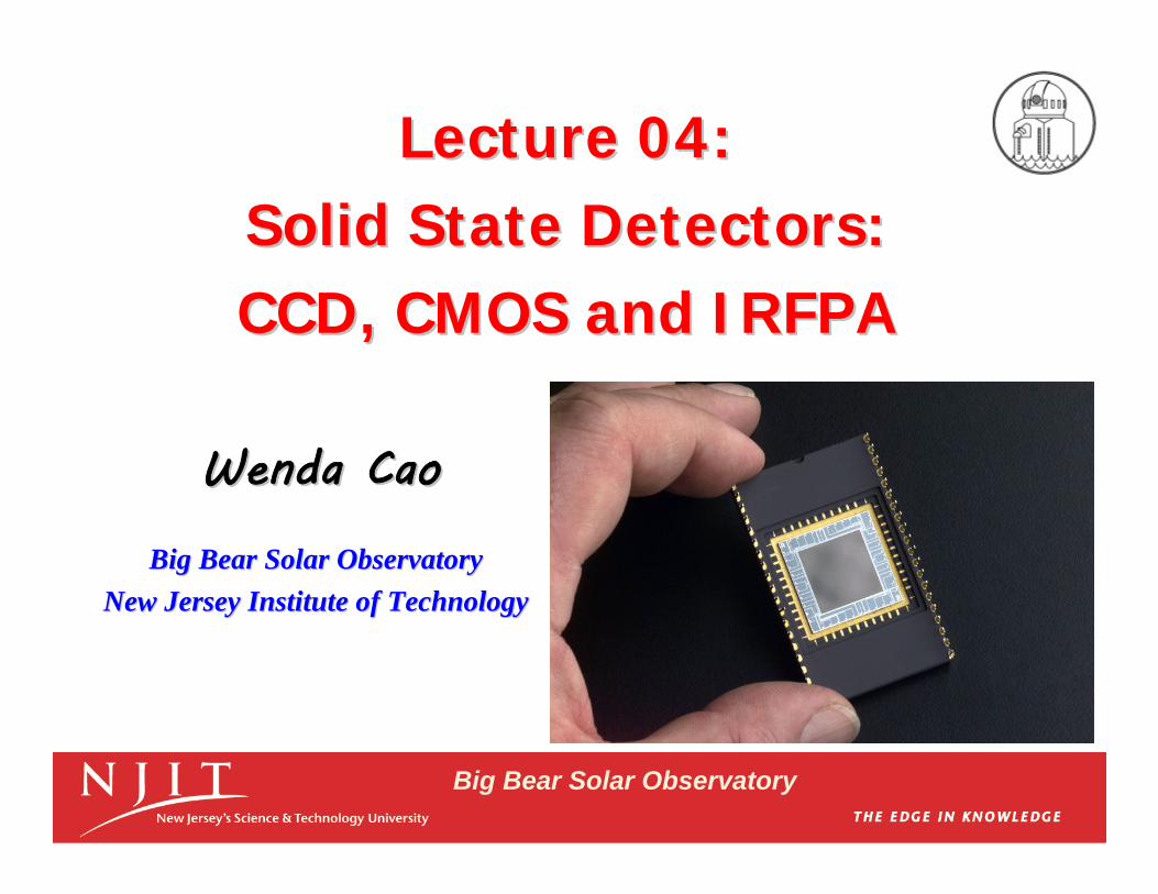
Lecture 04:Lecture 04:Solid State Detectors:Solid State Detectors:CCD, CMOS and IRFPACCD, CMOS and IRFPA
WendaWenda CaoCao
Big Bear Solar Observatory Big Bear Solar Observatory New Jersey Institute of TechnologyNew Jersey Institute of Technology
Big Bear Solar Observatory
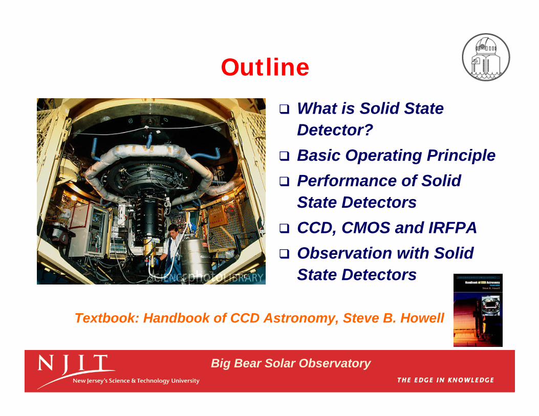
Outline What is Solid State
Detector? Basic Operating Principle Performance of Solid
State Detectors CCD, CMOS and IRFPA Observation with Solid
State Detectors
Textbook: Handbook of CCD Astronomy, Steve B. Howell
Big Bear Solar Observatory
1. Introduction
History What are Solid State Detectors?
CCD – Charge Coupling Device CMOS – Complementary Metal Oxide
Semiconductor IRFPA – Infrared Focal Plane Array
Why Use Solid State Detectors for Astronomical Imaging ? Naked eyes Films
Big Bear Solar Observatory
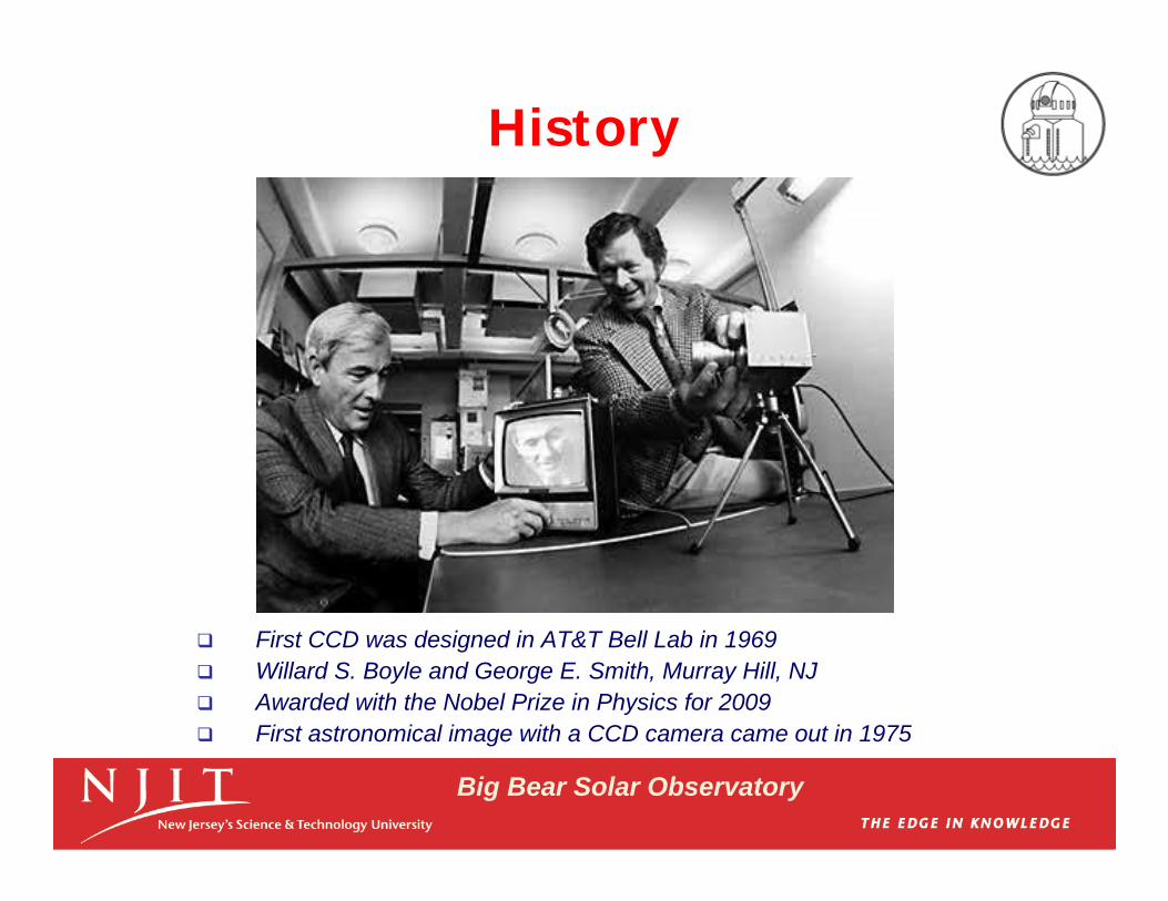
History
First CCD was designed in AT&T Bell Lab in 1969 Willard S. Boyle and George E. Smith, Murray Hill, NJ Awarded with the Nobel Prize in Physics for 2009 First astronomical image with a CCD camera came out in 1975
Big Bear Solar Observatory
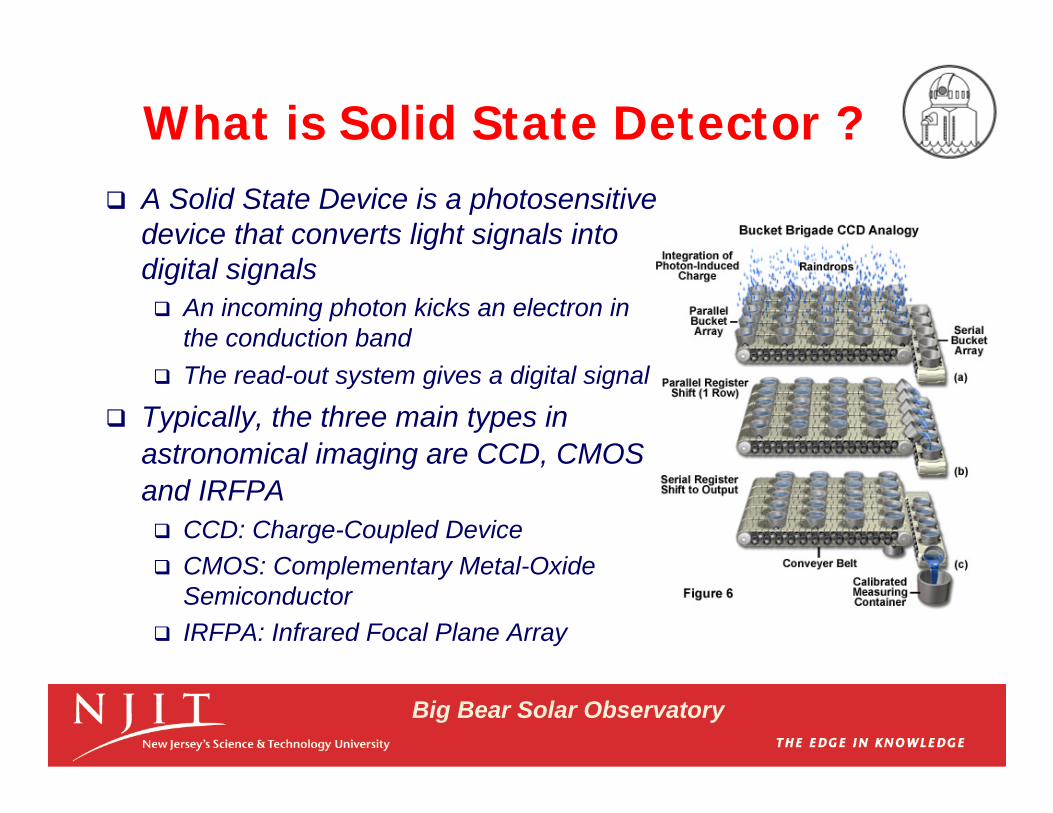
What is Solid State Detector ? A Solid State Device is a photosensitive
device that converts light signals into digital signals An incoming photon kicks an electron in
the conduction band The read-out system gives a digital signal
Typically, the three main types in astronomical imaging are CCD, CMOS and IRFPA CCD: Charge-Coupled Device CMOS: Complementary Metal-Oxide
Semiconductor IRFPA: Infrared Focal Plane Array
Big Bear Solar Observatory
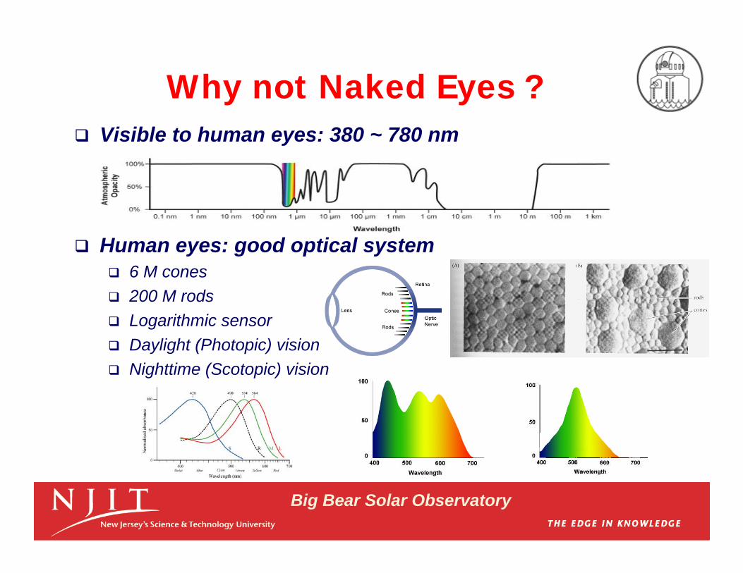
Visible to human eyes: 380 ~ 780 nm
Human eyes: good optical system 6 M cones 200 M rods Logarithmic sensor Daylight (Photopic) vision Nighttime (Scotopic) vision
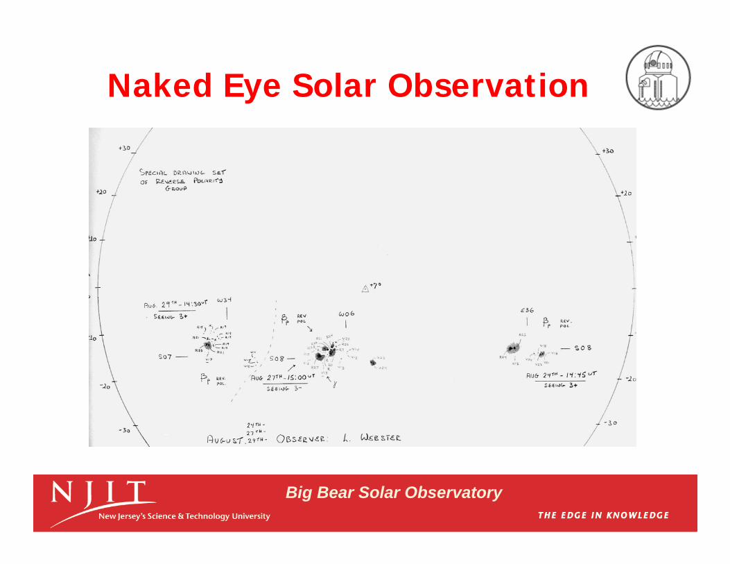
Why not Naked Eyes ?
Big Bear Solar Observatory
Naked Eye Solar Observation
Big Bear Solar Observatory
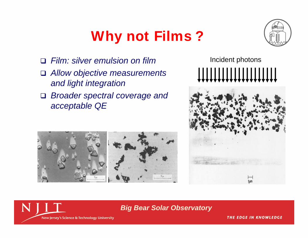
Why not Films ?
Film: silver emulsion on film Allow objective measurements
and light integration Broader spectral coverage and
acceptable QE
Incident photons
Big Bear Solar Observatory
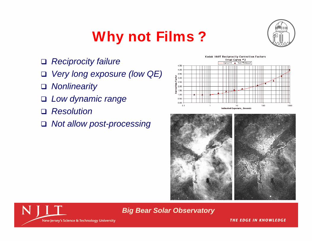
Why not Films ?
Reciprocity failure Very long exposure (low QE) Nonlinearity Low dynamic range Resolution Not allow post-processing
Big Bear Solar Observatory
Pros and ConsFilms reciprocity failure beyond a few second exposure minimal light intensity required to detect a target at all low quantum efficiency ( 5 ~ 20% at optimal wavelengths ) response to light is non-linear small dynamic range (6-bit) picture elements (grain) are randomly distributed needs to be processed in a chemical darkroom good MTF
Solid State Devices no loss of sensitivity to light during exposure no minimal light intensity required to detect a target high efficiency of light detection (up to 50 ~ 90%, though device-and wavelength-dependent) signal is proportional to light intensity large dynamic range (typically 16-bit) picture elements (pixels) are regularly spaced ready for digital processing
Big Bear Solar Observatory
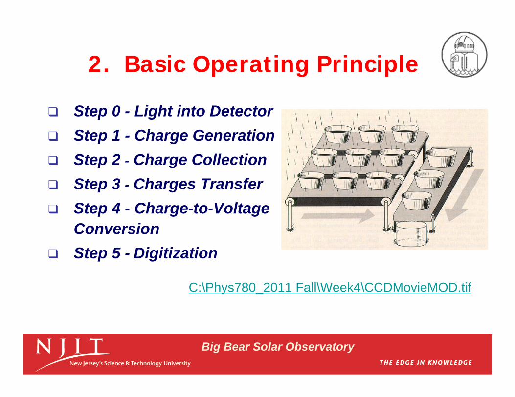
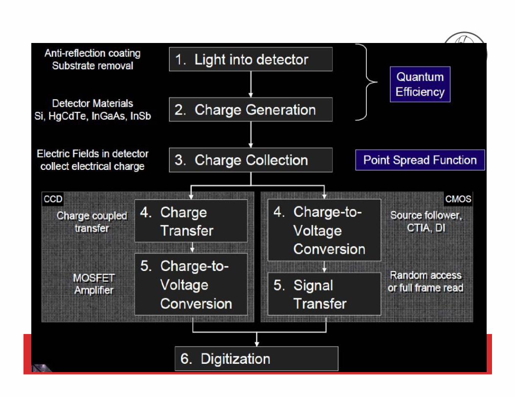
2. Basic Operating Principle
Step 0 - Light into Detector Step 1 - Charge Generation Step 2 - Charge Collection Step 3 - Charges Transfer Step 4 - Charge-to-Voltage
Conversion Step 5 - Digitization
C:\Phys780_2011 Fall\Week4\CCDMovieMOD.tif
Big Bear Solar Observatory
C:\Phys780_2011 Fall\Week4\CCDMovieMOD.tif
Big Bear Solar Observatory
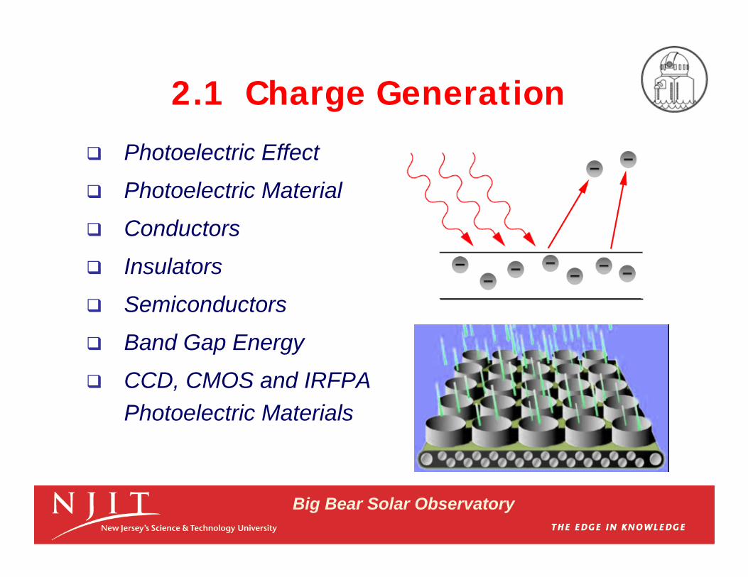
2.1 Charge Generation
Photoelectric Effect
Photoelectric Material
Conductors
Insulators
Semiconductors
Band Gap Energy
CCD, CMOS and IRFPA Photoelectric Materials
Big Bear Solar Observatory
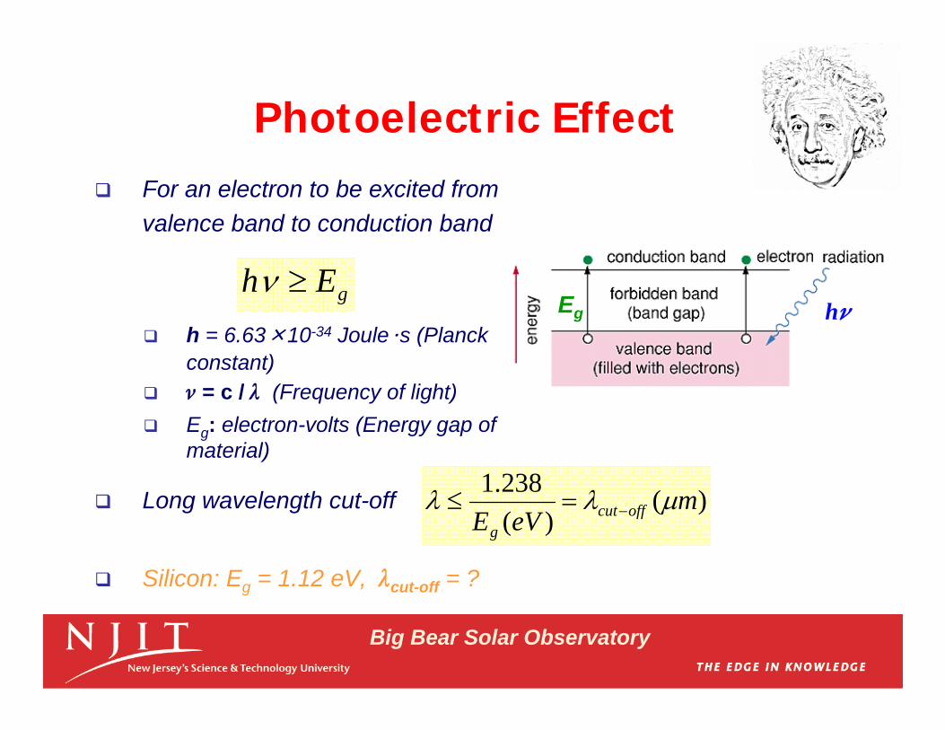
Photoelectric Effect For an electron to be excited from
valence band to conduction band
h = 6.63×10⁻³⁴ Joules (Planck constant)
= c / (Frequency of light) Eg: electron-volts (Energy gap of
material)
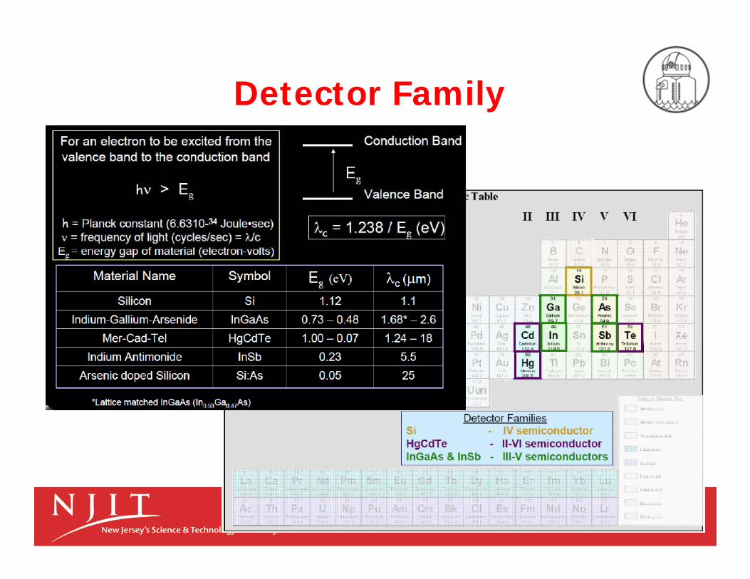
Long wavelength cut-off
Silicon: Eg = 1.12 eV, cut-off = ?
gEh hEg
)()(
238.1 meVE offcut
g
Big Bear Solar Observatory
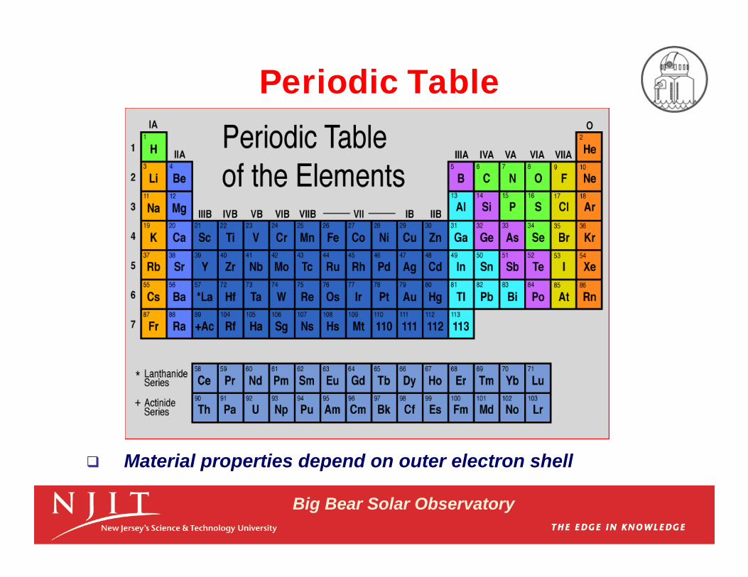
Periodic Table
Material properties depend on outer electron shell
Big Bear Solar Observatory
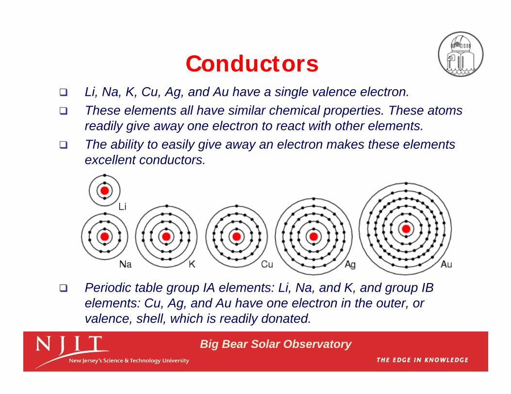
Li, Na, K, Cu, Ag, and Au have a single valence electron. These elements all have similar chemical properties. These atoms
readily give away one electron to react with other elements. The ability to easily give away an electron makes these elements
excellent conductors.
Periodic table group IA elements: Li, Na, and K, and group IB elements: Cu, Ag, and Au have one electron in the outer, or valence, shell, which is readily donated.
Conductors
Big Bear Solar Observatory
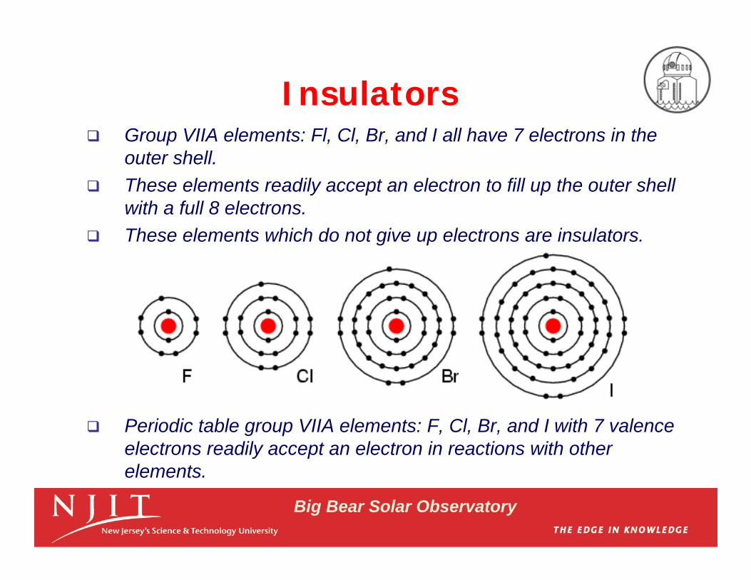
Group VIIA elements: Fl, Cl, Br, and I all have 7 electrons in the outer shell.
These elements readily accept an electron to fill up the outer shell with a full 8 electrons.
These elements which do not give up electrons are insulators.
Periodic table group VIIA elements: F, Cl, Br, and I with 7 valence electrons readily accept an electron in reactions with other elements.
Insulators
Big Bear Solar Observatory
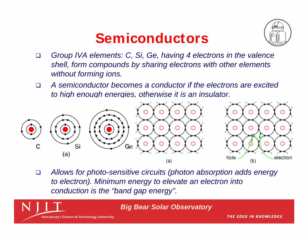
Group IVA elements: C, Si, Ge, having 4 electrons in the valence shell, form compounds by sharing electrons with other elements without forming ions.
A semiconductor becomes a conductor if the electrons are excitedto high enough energies, otherwise it is an insulator.
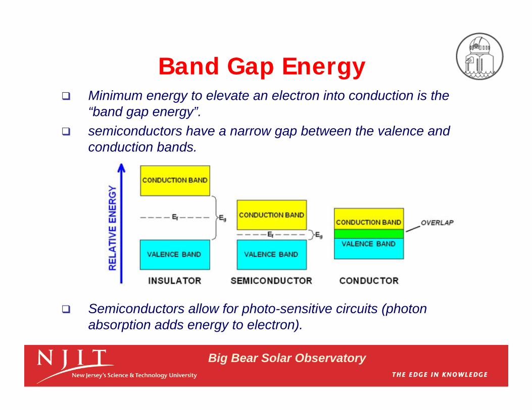
Allows for photo-sensitive circuits (photon absorption adds energy to electron). Minimum energy to elevate an electron into conduction is the “band gap energy”.
Semiconductors
Big Bear Solar Observatory
Minimum energy to elevate an electron into conduction is the “band gap energy”.
semiconductors have a narrow gap between the valence and conduction bands.
Semiconductors allow for photo-sensitive circuits (photon absorption adds energy to electron).
Band Gap Energy
Big Bear Solar Observatory
Detector Family
Big Bear Solar Observatory
2.2 Charge Collection
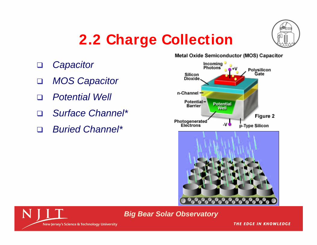
Capacitor
MOS Capacitor
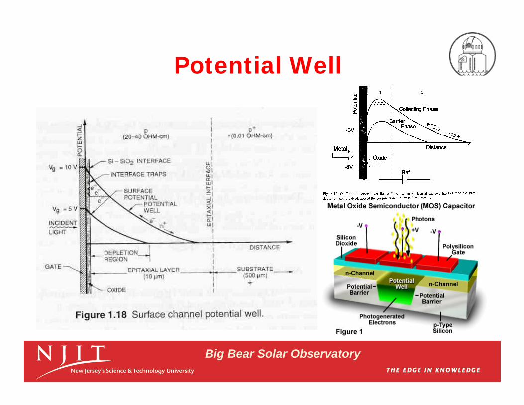
Potential Well
Surface Channel*
Buried Channel*
Big Bear Solar Observatory
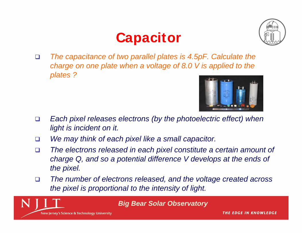
Capacitor The capacitance of two parallel plates is 4.5pF. Calculate the
charge on one plate when a voltage of 8.0 V is applied to the plates ?
Each pixel releases electrons (by the photoelectric effect) whenlight is incident on it.
We may think of each pixel like a small capacitor. The electrons released in each pixel constitute a certain amount of
charge Q, and so a potential difference V develops at the ends of the pixel.
The number of electrons released, and the voltage created acrossthe pixel is proportional to the intensity of light.
Big Bear Solar Observatory
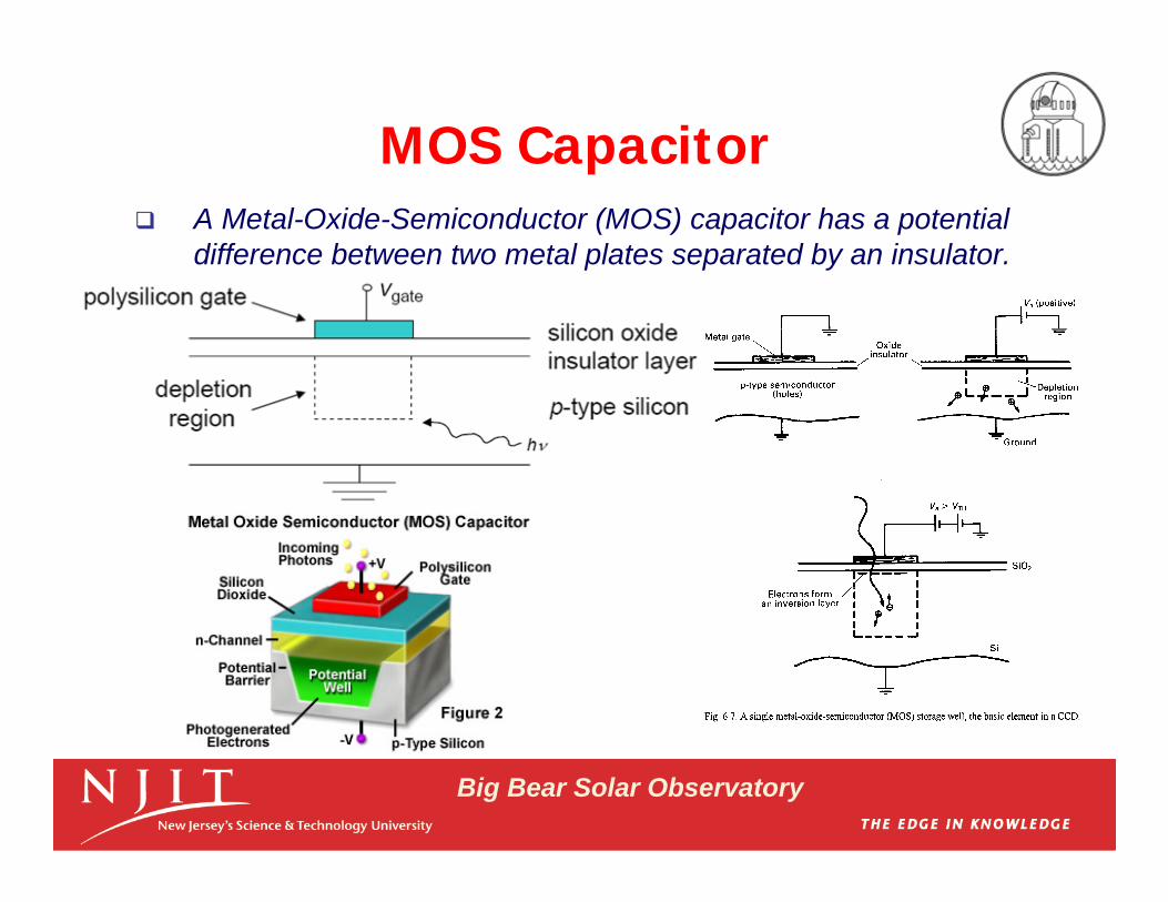
MOS Capacitor A Metal-Oxide-Semiconductor (MOS) capacitor has a potential
difference between two metal plates separated by an insulator.
Big Bear Solar Observatory
Potential Well
Big Bear Solar Observatory
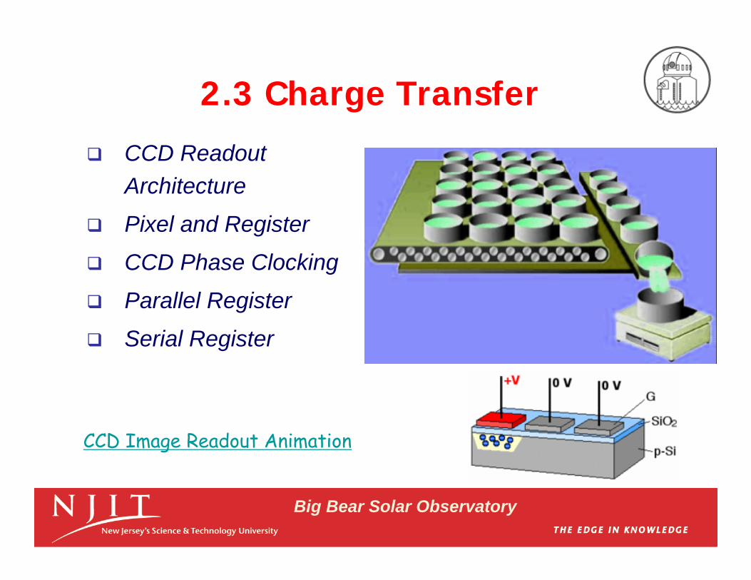
2.3 Charge Transfer
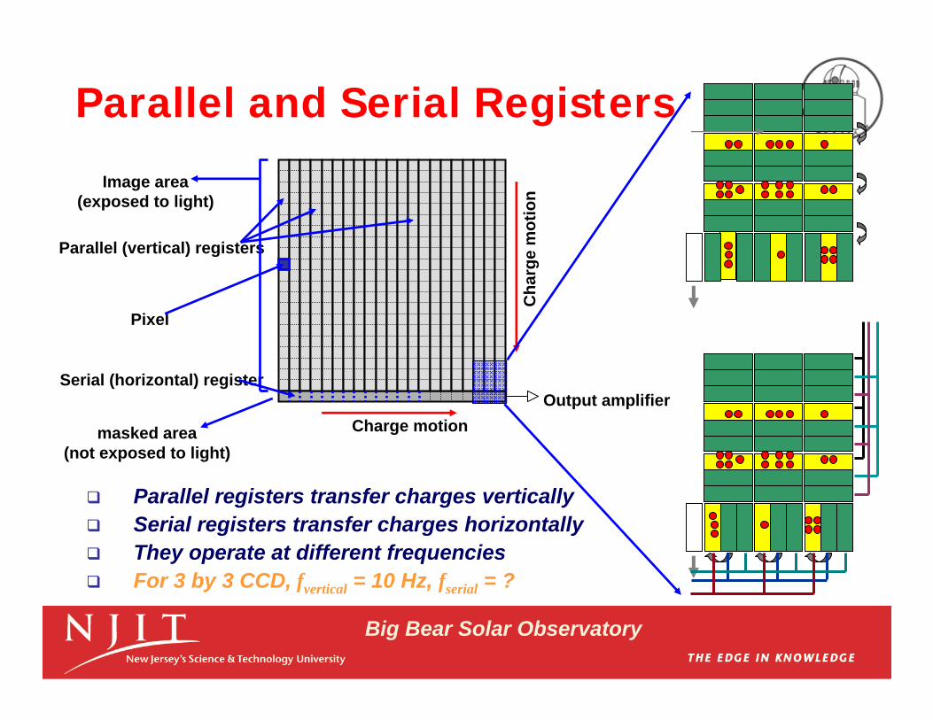
CCD Readout Architecture
Pixel and Register
CCD Phase Clocking
Parallel Register
Serial Register
CCD Image Readout Animation
Big Bear Solar Observatory
Big Bear Solar Observatory
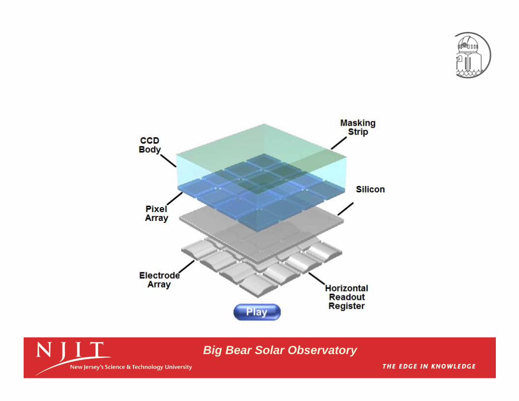
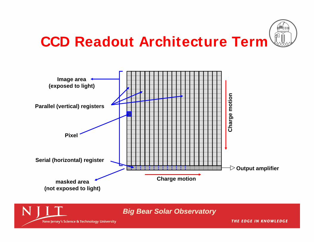
CCD Readout Architecture Term
Charge motion
Cha
rge
mot
ion
Serial (horizontal) register
Parallel (vertical) registers
Pixel
Image area(exposed to light)
Output amplifier
masked area(not exposed to light)
Big Bear Solar Observatory
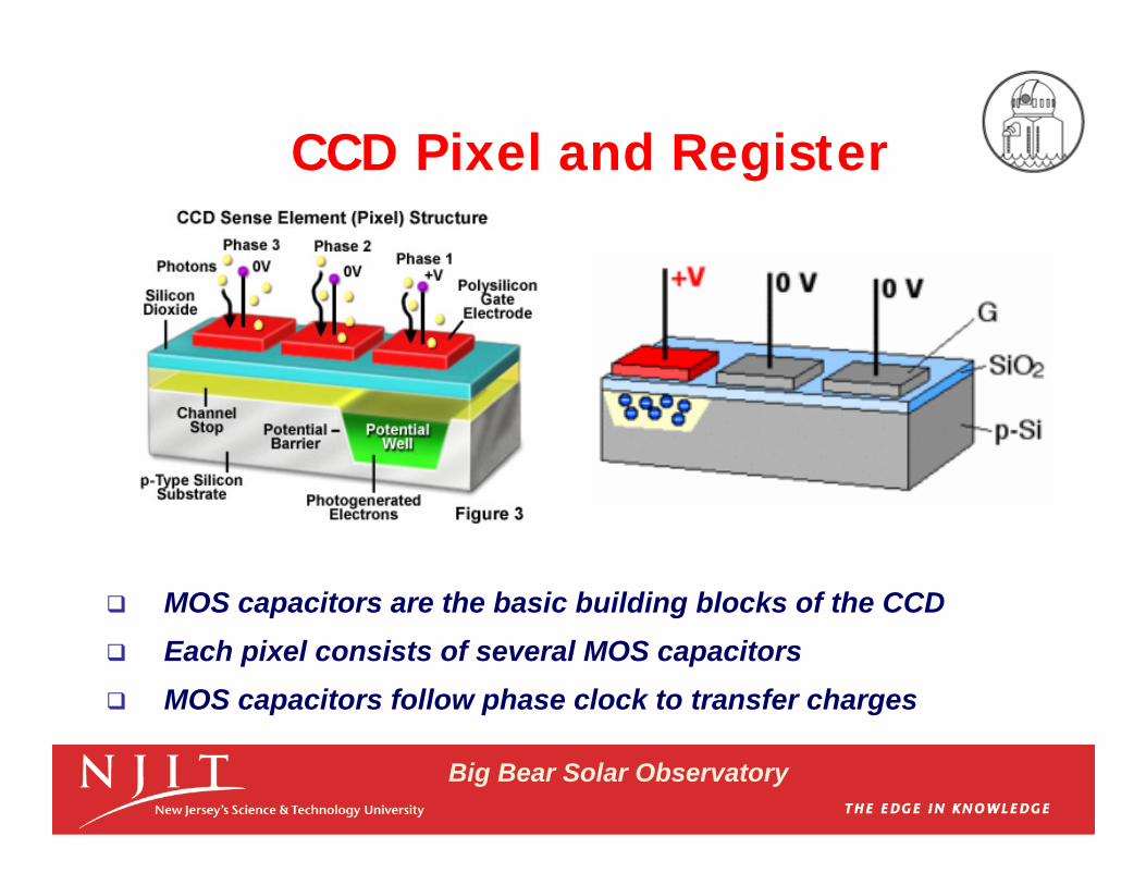
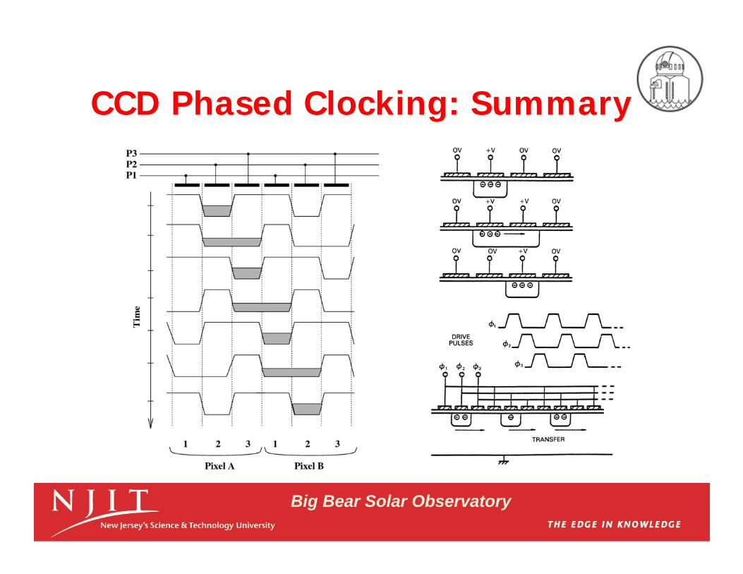
CCD Pixel and Register
MOS capacitors are the basic building blocks of the CCD Each pixel consists of several MOS capacitors MOS capacitors follow phase clock to transfer charges
Big Bear Solar Observatory pi
xel
boun
dary
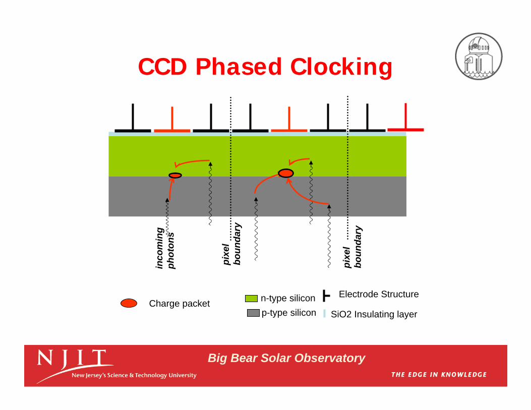
Charge packetp-type siliconn-type silicon
SiO2 Insulating layer
Electrode Structure
pixe
l bo
unda
ry
inco
min
gph
oton
s
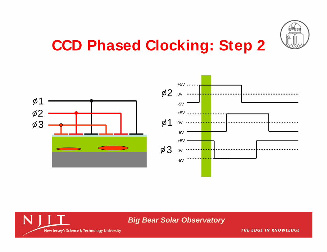
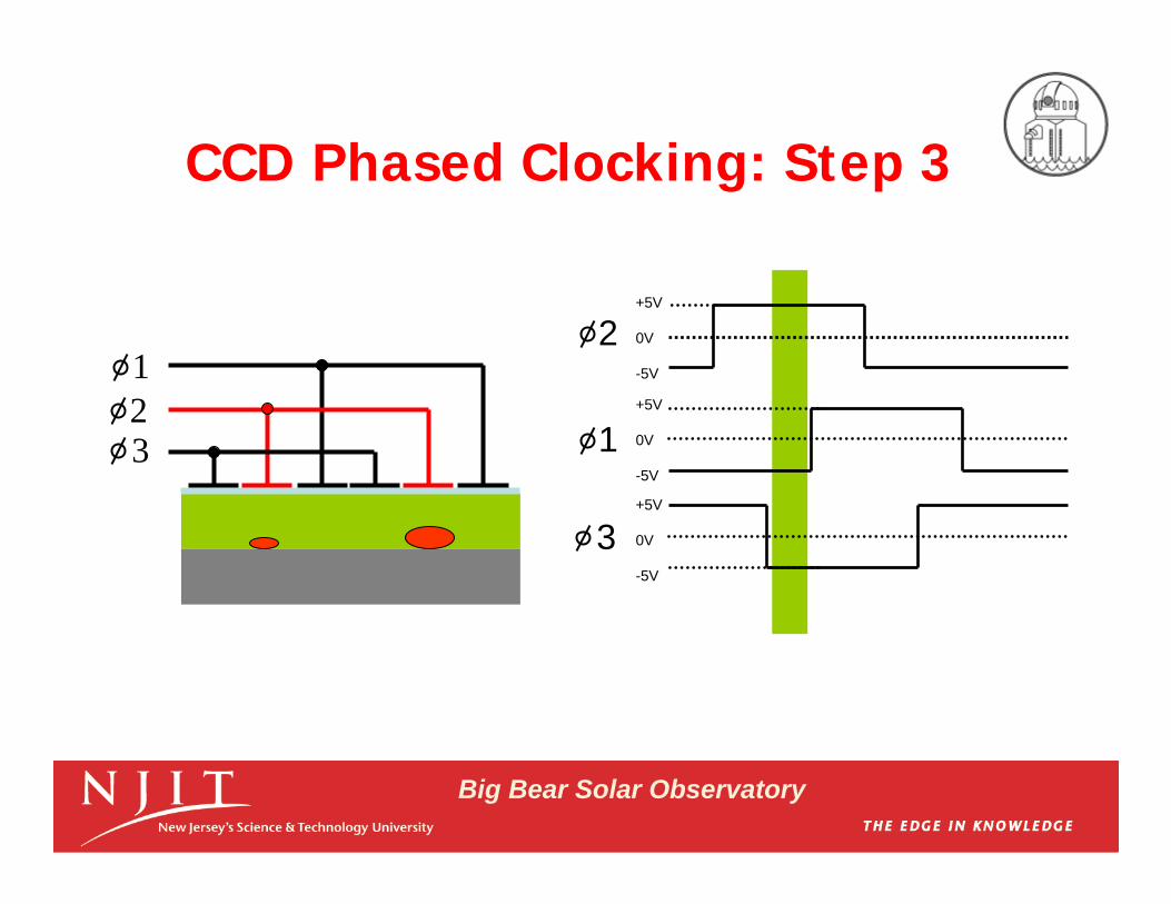
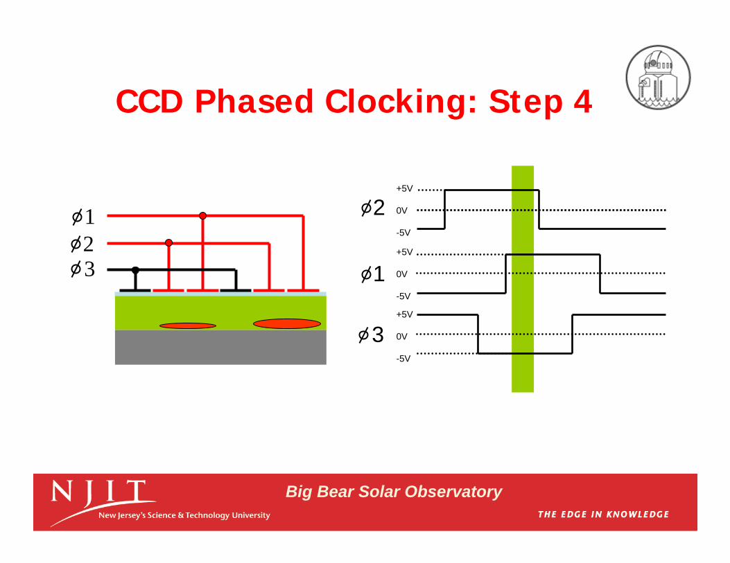
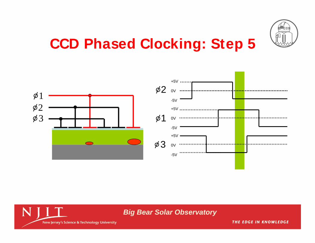
CCD Phased Clocking
Big Bear Solar Observatory
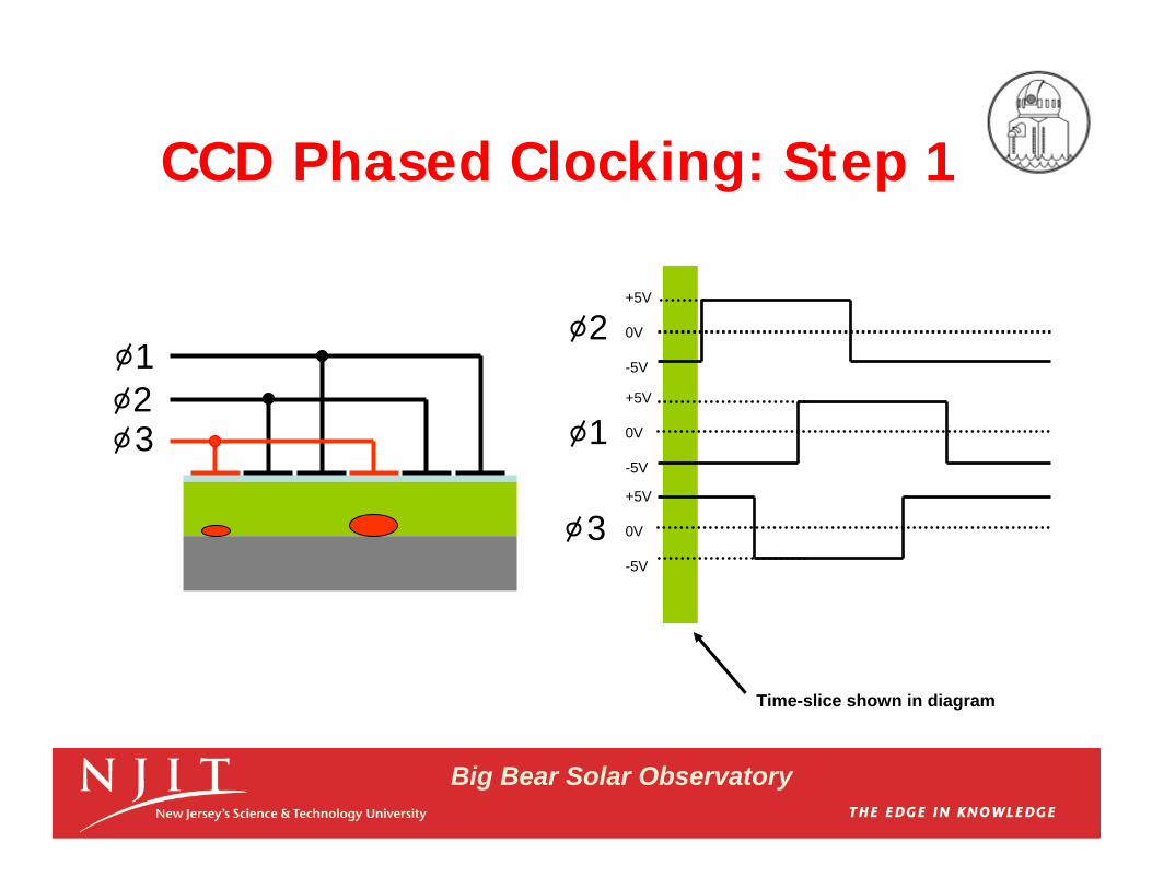
123
Time-slice shown in diagram
+5V
0V
-5V
+5V
0V
-5V
+5V
0V
-5V
1
2
3
CCD Phased Clocking: Step 1
Big Bear Solar Observatory
123
CCD Phased Clocking: Step 2
+5V
0V
-5V
+5V
0V
-5V
+5V
0V
-5V
1
2
3
Big Bear Solar Observatory
123
CCD Phased Clocking: Step 3
+5V
0V
-5V
+5V
0V
-5V
+5V
0V
-5V
1
2
3
Big Bear Solar Observatory
123
CCD Phased Clocking: Step 4
+5V
0V
-5V
+5V
0V
-5V
+5V
0V
-5V
1
2
3
Big Bear Solar Observatory
123
CCD Phased Clocking: Step 5
+5V
0V
-5V
+5V
0V
-5V
+5V
0V
-5V
1
2
3
Big Bear Solar Observatory
CCD Phased Clocking: Summary
Big Bear Solar Observatory
Parallel and Serial Registers
Charge motion
Cha
rge
mot
ion
Serial (horizontal) register
Parallel (vertical) registers
Pixel
Image area(exposed to light)
Output amplifier
masked area(not exposed to light)
Parallel registers transfer charges vertically Serial registers transfer charges horizontally They operate at different frequencies For 3 by 3 CCD, fvertical = 10 Hz, fserial = ?
Big Bear Solar Observatory
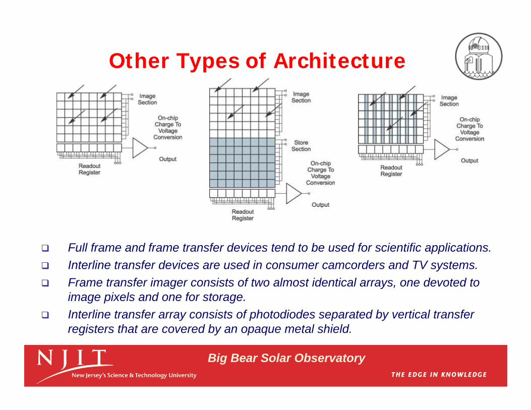
Other Types of Architecture
Full frame and frame transfer devices tend to be used for scientific applications. Interline transfer devices are used in consumer camcorders and TV systems. Frame transfer imager consists of two almost identical arrays, one devoted to
image pixels and one for storage. Interline transfer array consists of photodiodes separated by vertical transfer
registers that are covered by an opaque metal shield.
Big Bear Solar Observatory
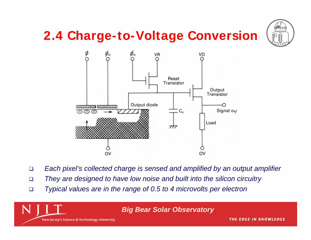
2.4 Charge-to-Voltage Conversion
Each pixel’s collected charge is sensed and amplified by an output amplifier They are designed to have low noise and built into the silicon circuitry Typical values are in the range of 0.5 to 4 microvolts per electron
Big Bear Solar Observatory
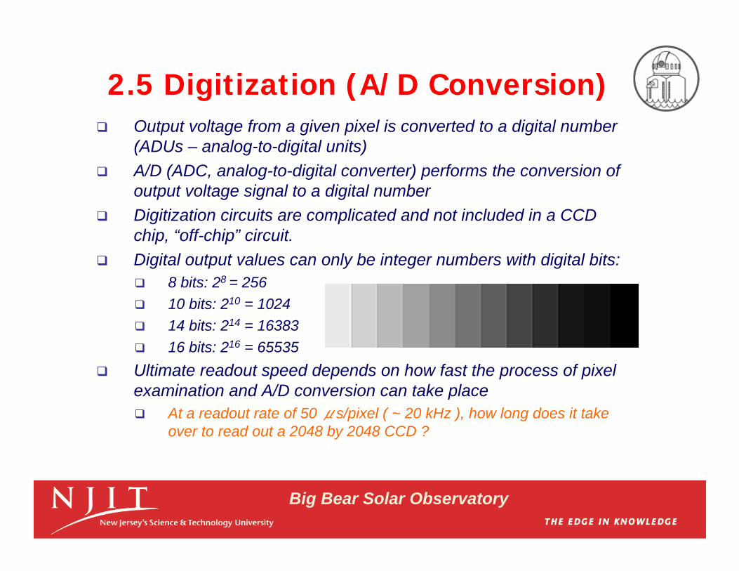
2.5 Digitization (A/D Conversion) Output voltage from a given pixel is converted to a digital number
(ADUs – analog-to-digital units) A/D (ADC, analog-to-digital converter) performs the conversion of
output voltage signal to a digital number Digitization circuits are complicated and not included in a CCD
chip, “off-chip” circuit. Digital output values can only be integer numbers with digital bits:
8 bits: 28 = 256 10 bits: 210 = 1024 14 bits: 214 = 16383 16 bits: 216 = 65535
Ultimate readout speed depends on how fast the process of pixel examination and A/D conversion can take place At a readout rate of 50 μs/pixel ( ~ 20 kHz ), how long does it take
over to read out a 2048 by 2048 CCD ?
Big Bear Solar Observatory
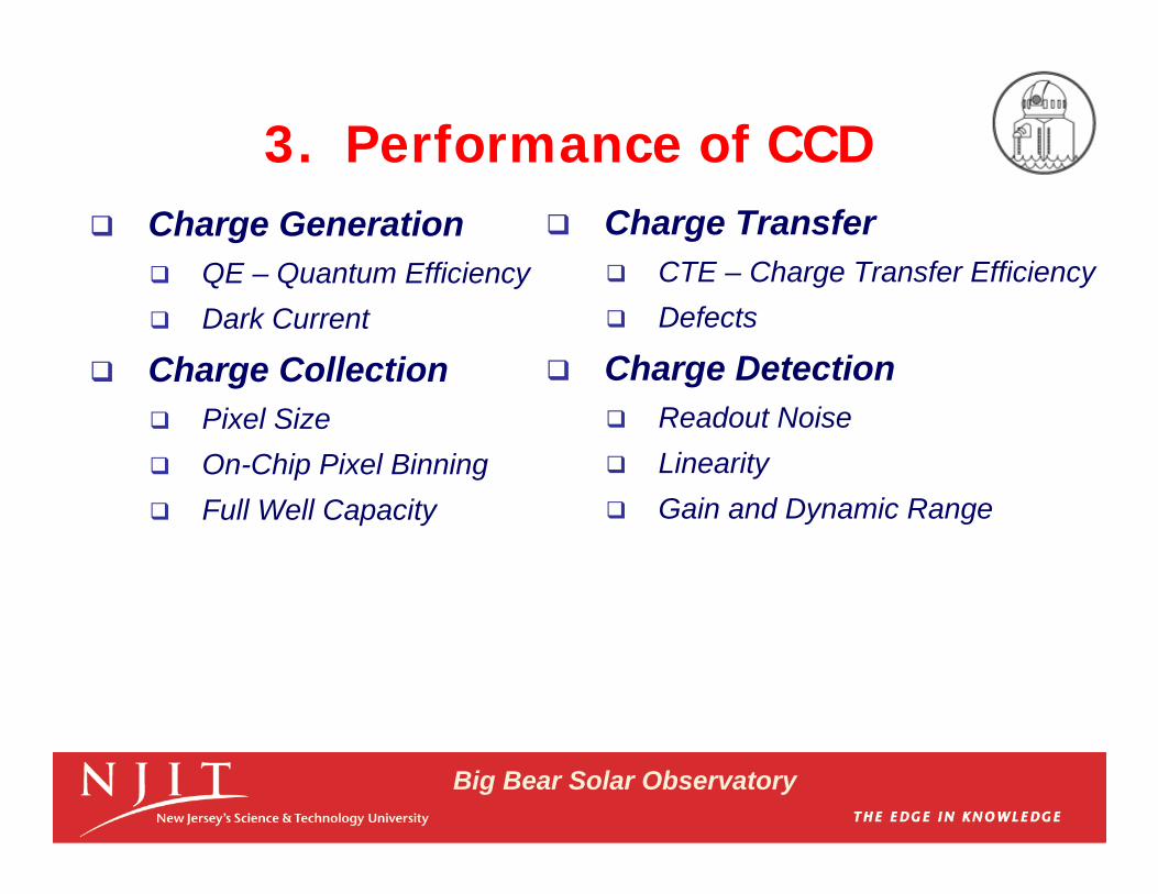
3. Performance of CCD Charge Generation
QE – Quantum Efficiency Dark Current
Charge Collection Pixel Size On-Chip Pixel Binning Full Well Capacity
Charge Transfer CTE – Charge Transfer Efficiency Defects
Charge Detection Readout Noise Linearity Gain and Dynamic Range
Big Bear Solar Observatory
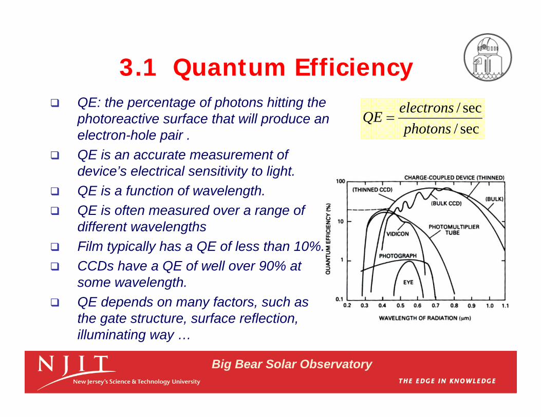
QE: the percentage of photons hitting the photoreactive surface that will produce an electron-hole pair .
QE is an accurate measurement of device’s electrical sensitivity to light.
QE is a function of wavelength. QE is often measured over a range of
different wavelengths Film typically has a QE of less than 10%. CCDs have a QE of well over 90% at
some wavelength. QE depends on many factors, such as
the gate structure, surface reflection, illuminating way …
3.1 Quantum Efficiency
sec/sec/
photonselectronsQE
Big Bear Solar Observatory
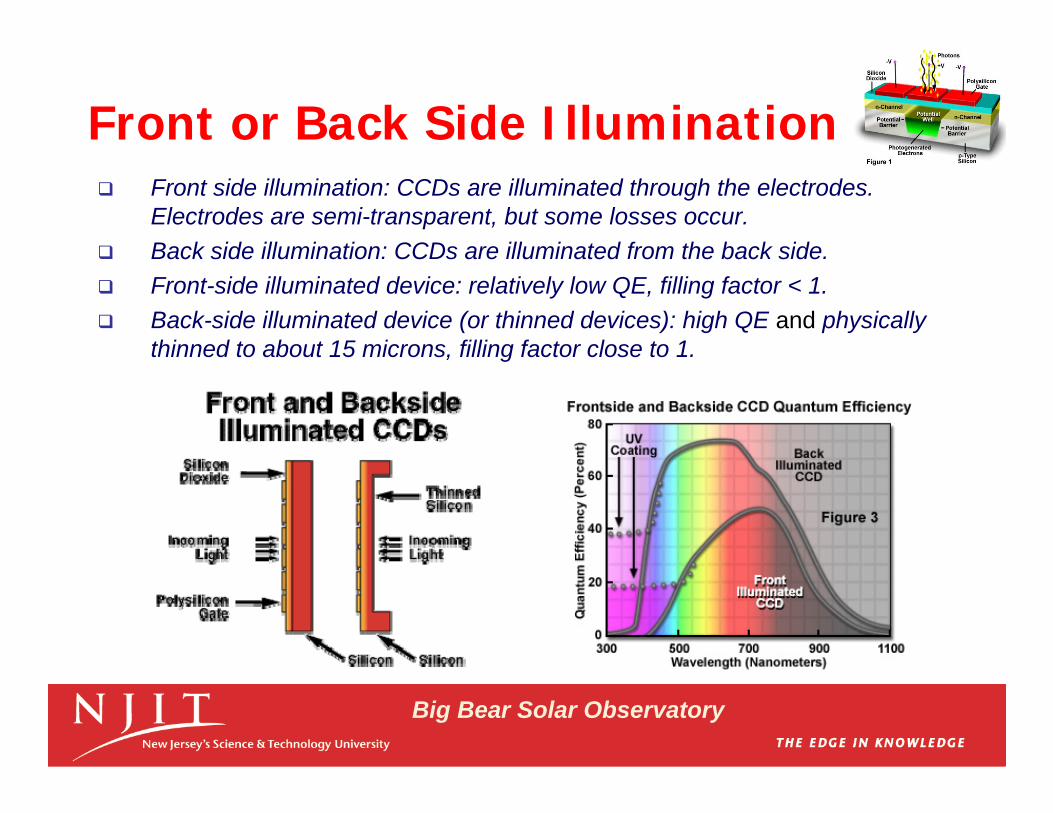
Front side illumination: CCDs are illuminated through the electrodes. Electrodes are semi-transparent, but some losses occur.
Back side illumination: CCDs are illuminated from the back side. Front-side illuminated device: relatively low QE, filling factor < 1. Back-side illuminated device (or thinned devices): high QE and physically
thinned to about 15 microns, filling factor close to 1.
Front or Back Side Illumination
Big Bear Solar Observatory
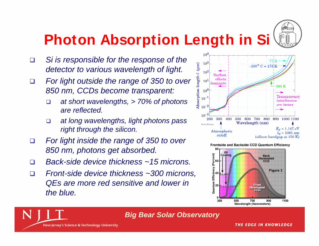
Photon Absorption Length in Si Si is responsible for the response of the
detector to various wavelength of light. For light outside the range of 350 to over
850 nm, CCDs become transparent: at short wavelengths, > 70% of photons
are reflected. at long wavelengths, light photons pass
right through the silicon. For light inside the range of 350 to over
850 nm, photons get absorbed. Back-side device thickness ~15 microns. Front-side device thickness ~300 microns,
QEs are more red sensitive and lower in the blue.
Big Bear Solar Observatory
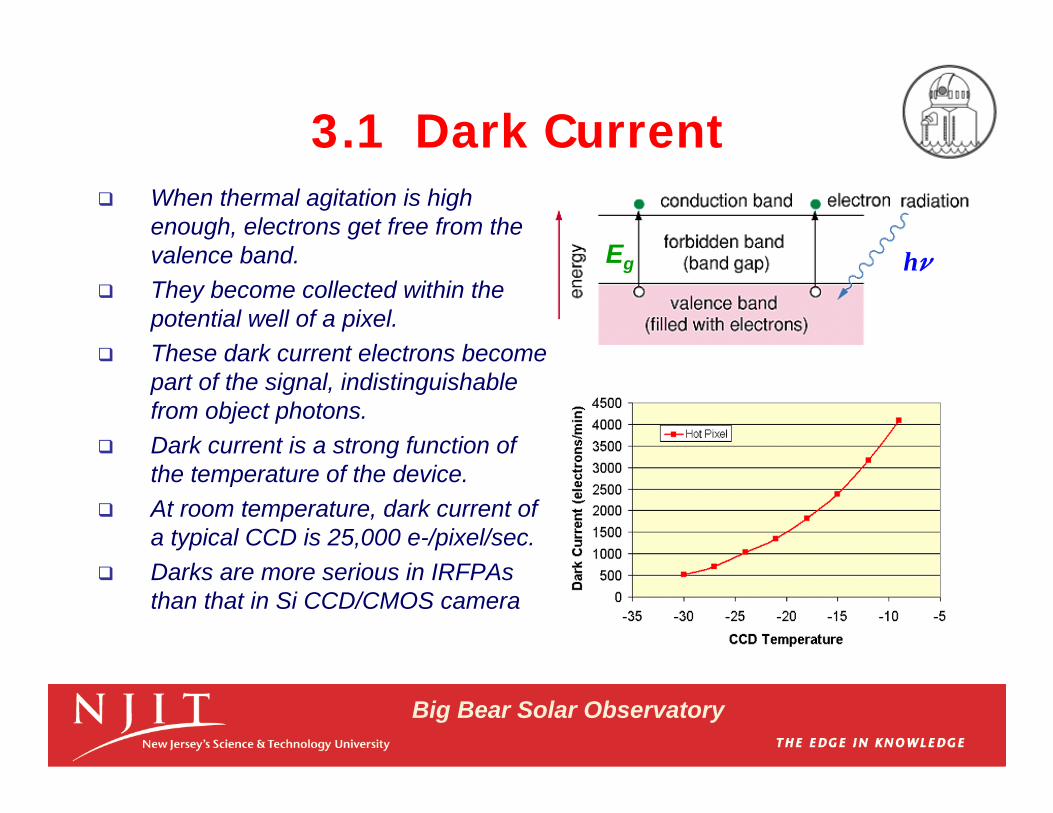
When thermal agitation is high enough, electrons get free from the valence band.
They become collected within the potential well of a pixel.
These dark current electrons become part of the signal, indistinguishable from object photons.
Dark current is a strong function of the temperature of the device.
At room temperature, dark current of a typical CCD is 25,000 e-/pixel/sec.
Darks are more serious in IRFPAsthan that in Si CCD/CMOS camera
3.1 Dark Current
hEg
Big Bear Solar Observatory
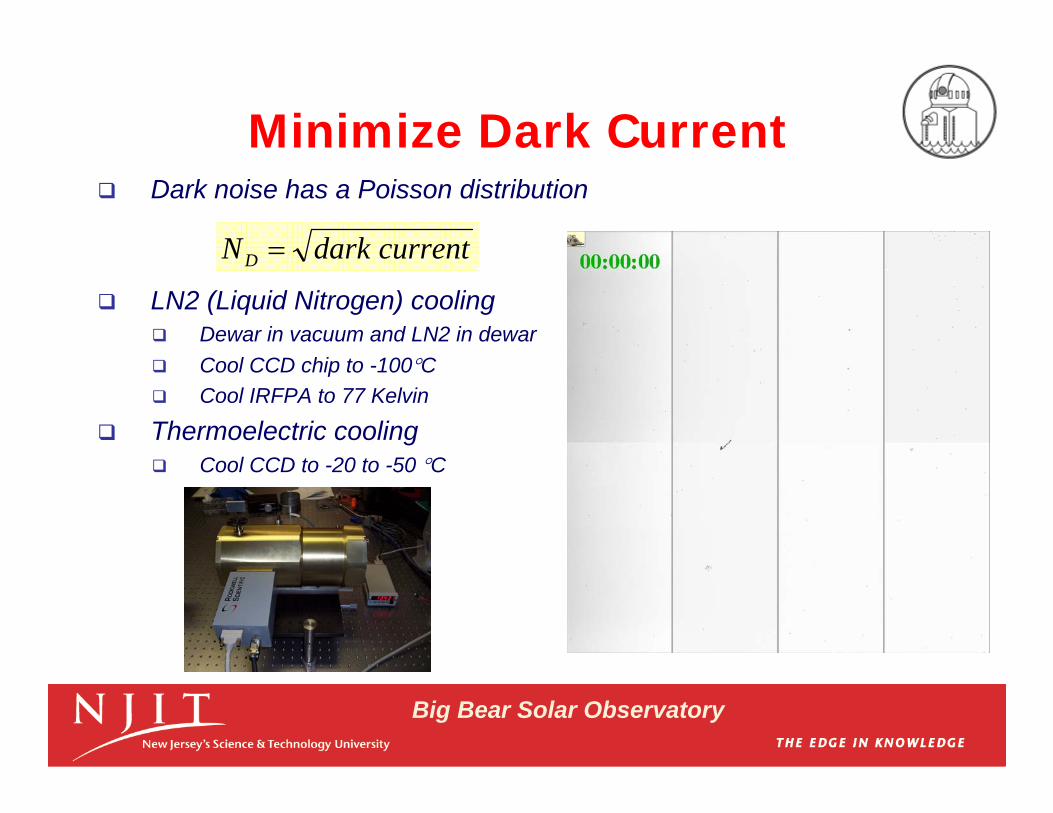
Dark noise has a Poisson distribution
LN2 (Liquid Nitrogen) cooling Dewar in vacuum and LN2 in dewar Cool CCD chip to -100C Cool IRFPA to 77 Kelvin
Thermoelectric cooling Cool CCD to -20 to -50 C
Minimize Dark Current
currentdarkND
Big Bear Solar Observatory
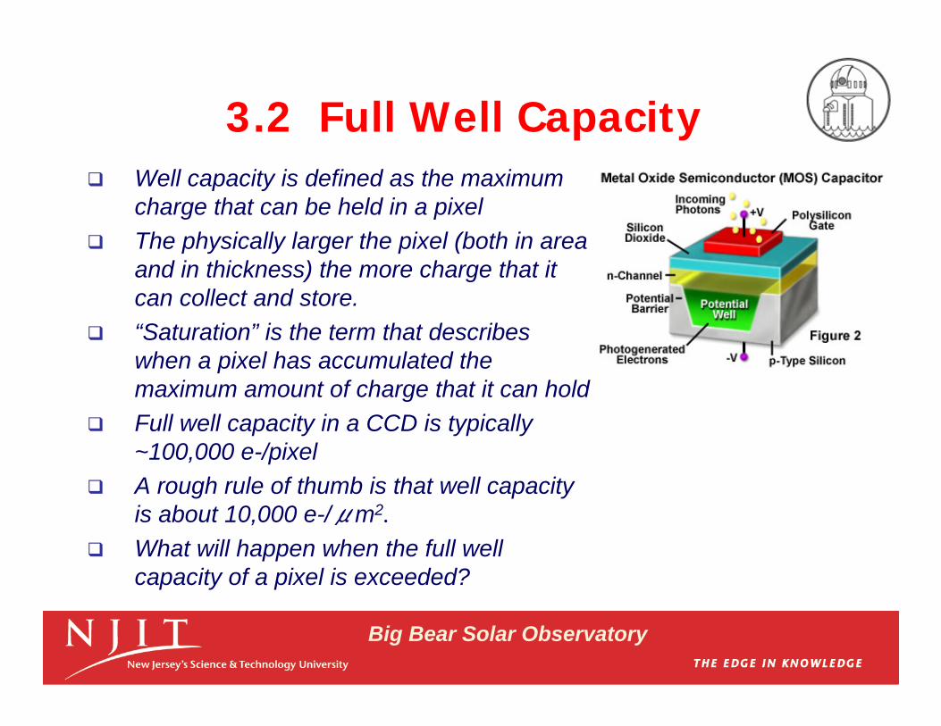
Well capacity is defined as the maximum charge that can be held in a pixel
The physically larger the pixel (both in area and in thickness) the more charge that it can collect and store.
“Saturation” is the term that describes when a pixel has accumulated the maximum amount of charge that it can hold
Full well capacity in a CCD is typically ~100,000 e-/pixel
A rough rule of thumb is that well capacity is about 10,000 e-/μm2.
What will happen when the full well capacity of a pixel is exceeded?
3.2 Full Well Capacity
Big Bear Solar Observatory
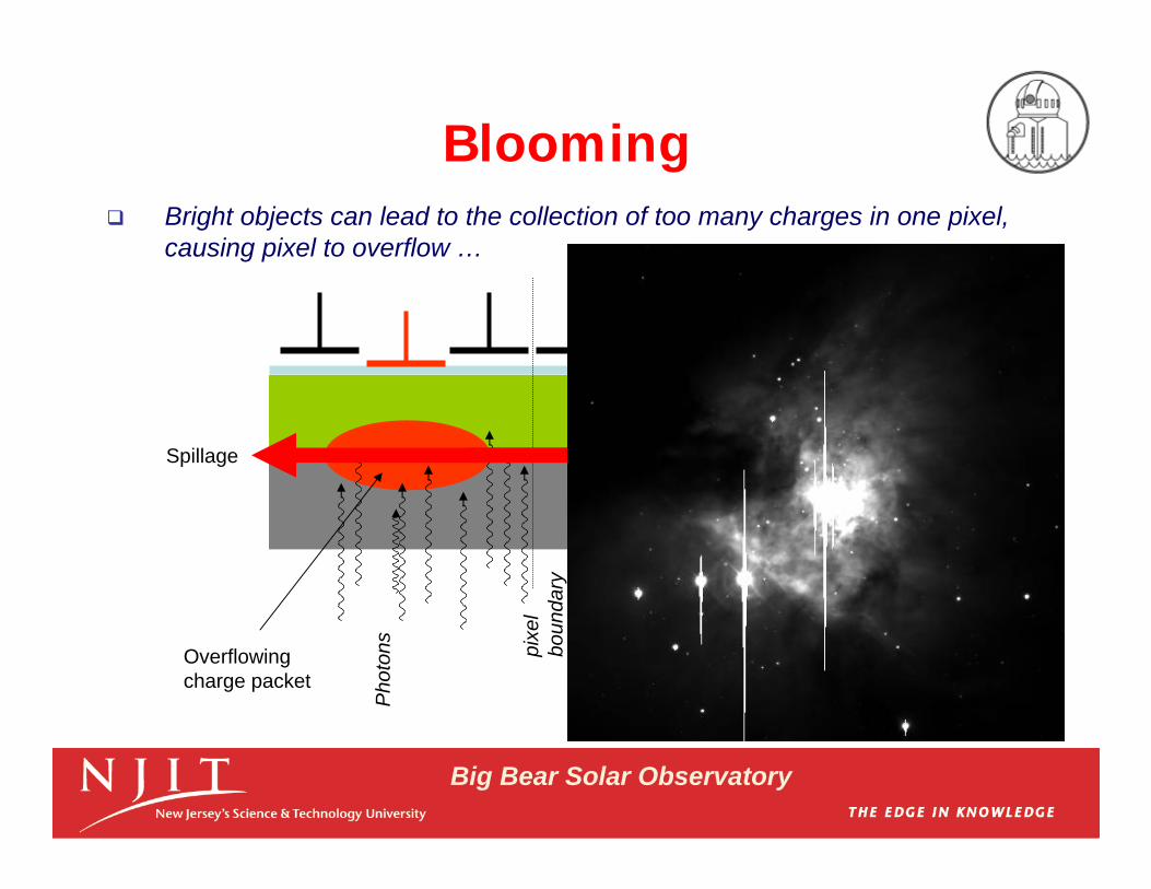
Blooming
pixe
l bo
unda
ry
Pho
tons
Pho
tonsOverflowing
charge packet
Spillage Spillage
pixe
l bo
unda
ry
Bright objects can lead to the collection of too many charges in one pixel, causing pixel to overflow …
Big Bear Solar Observatory
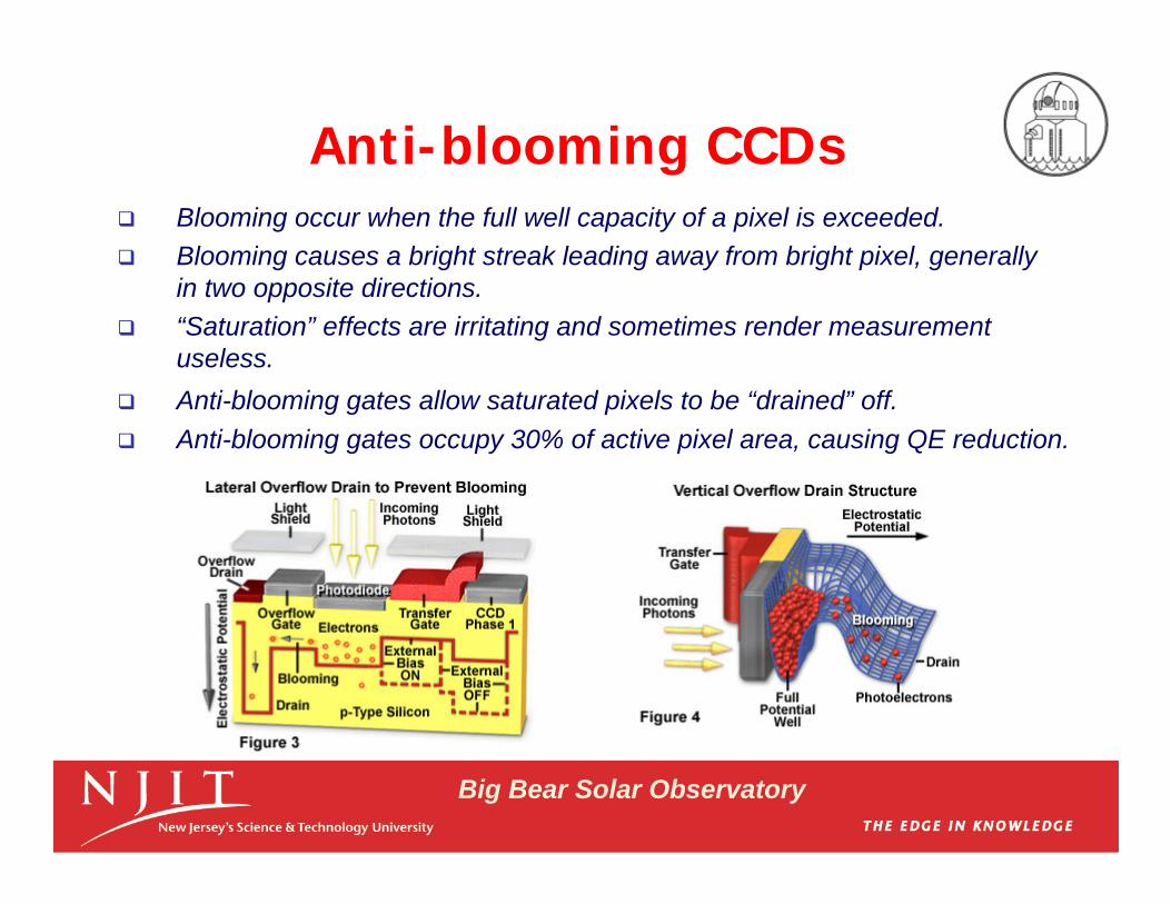
Blooming occur when the full well capacity of a pixel is exceeded. Blooming causes a bright streak leading away from bright pixel, generally
in two opposite directions. “Saturation” effects are irritating and sometimes render measurement
useless. Anti-blooming gates allow saturated pixels to be “drained” off. Anti-blooming gates occupy 30% of active pixel area, causing QE reduction.
Anti-blooming CCDs
Big Bear Solar Observatory
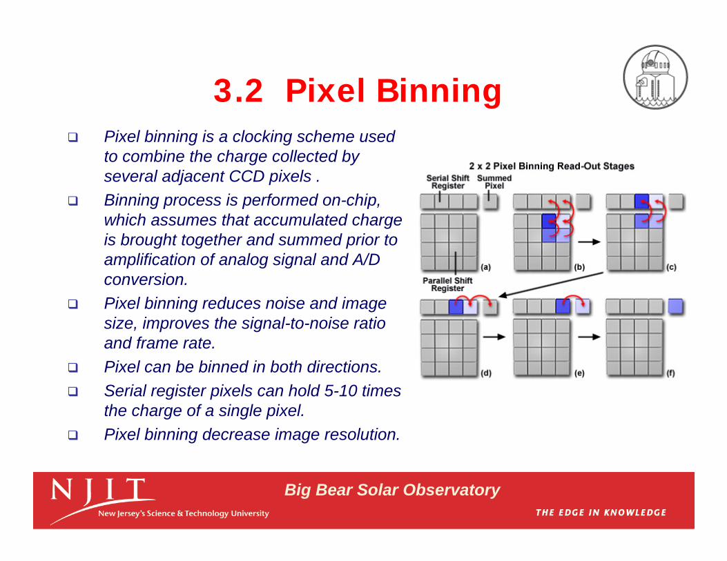
Pixel binning is a clocking scheme used to combine the charge collected by several adjacent CCD pixels .
Binning process is performed on-chip, which assumes that accumulated charge is brought together and summed prior to amplification of analog signal and A/D conversion.
Pixel binning reduces noise and image size, improves the signal-to-noise ratio and frame rate.
Pixel can be binned in both directions. Serial register pixels can hold 5-10 times
the charge of a single pixel. Pixel binning decrease image resolution.
3.2 Pixel Binning
Big Bear Solar Observatory
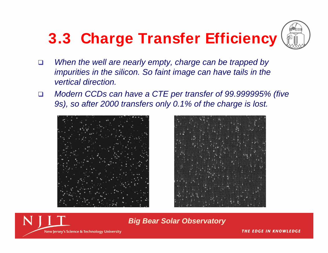
When the well are nearly empty, charge can be trapped by impurities in the silicon. So faint image can have tails in the vertical direction.
Modern CCDs can have a CTE per transfer of 99.999995% (five 9s), so after 2000 transfers only 0.1% of the charge is lost.
3.3 Charge Transfer Efficiency
Big Bear Solar Observatory
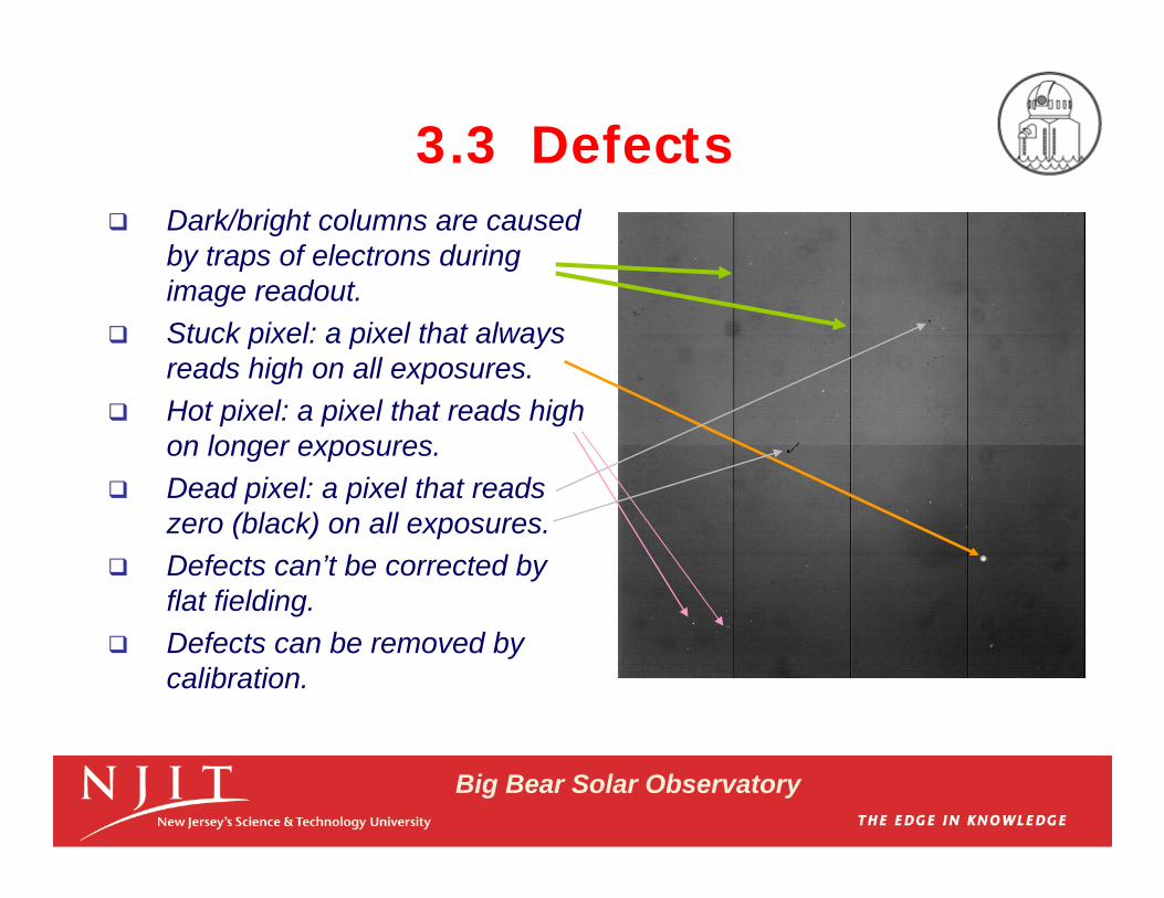
Dark/bright columns are caused by traps of electrons during image readout.
Stuck pixel: a pixel that always reads high on all exposures.
Hot pixel: a pixel that reads high on longer exposures.
Dead pixel: a pixel that reads zero (black) on all exposures.
Defects can’t be corrected by flat fielding.
Defects can be removed by calibration.
3.3 Defects
Big Bear Solar Observatory
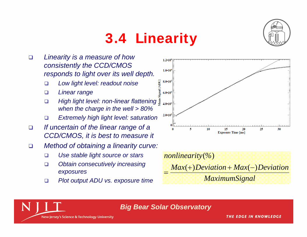
3.4 Linearity Linearity is a measure of how
consistently the CCD/CMOS responds to light over its well depth. Low light level: readout noise Linear range High light level: non-linear flattening
when the charge in the well > 80% Extremely high light level: saturation
If uncertain of the linear range of a CCD/CMOS, it is best to measure it
Method of obtaining a linearity curve: Use stable light source or stars Obtain consecutively increasing
exposures Plot output ADU vs. exposure time nalMaximumSig
DeviationMaxDeviationMax%tynonlineari
)()()(
Big Bear Solar Observatory
3.4 Gain Output voltage (electrons) from a given pixel is converted
to a digital number (ADUs – analog-to-digital units) Gain: amount of charge collected in each pixel will be
assigned to produce 1 ADU Gain = 10 e-/ADU: for 1509 e- coming, how many ADUs ?
Gain value: given in terms of the number of electrons needed to produce one ADU (e-/ADU)
Gain is set by the electronics that read out the CCD chip. Gain value is an average conversion ratio, based on
changing large numbers of electrons into large numbers of ADUs.
What does a gain of 1.8e-/ADU stand for?
Big Bear Solar Observatory
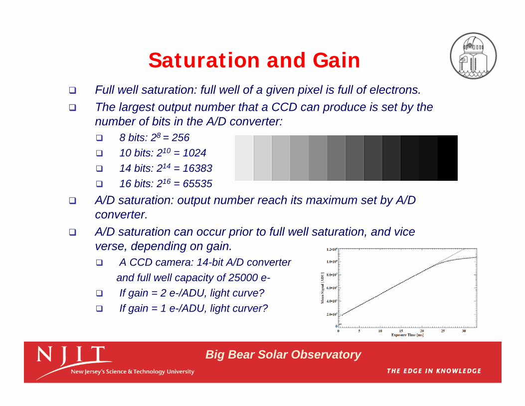
Saturation and Gain Full well saturation: full well of a given pixel is full of electrons. The largest output number that a CCD can produce is set by the
number of bits in the A/D converter: 8 bits: 28 = 256 10 bits: 210 = 1024 14 bits: 214 = 16383 16 bits: 216 = 65535
A/D saturation: output number reach its maximum set by A/D converter.
A/D saturation can occur prior to full well saturation, and viceverse, depending on gain. A CCD camera: 14-bit A/D converter
and full well capacity of 25000 e- If gain = 2 e-/ADU, light curve? If gain = 1 e-/ADU, light curver?
Big Bear Solar Observatory
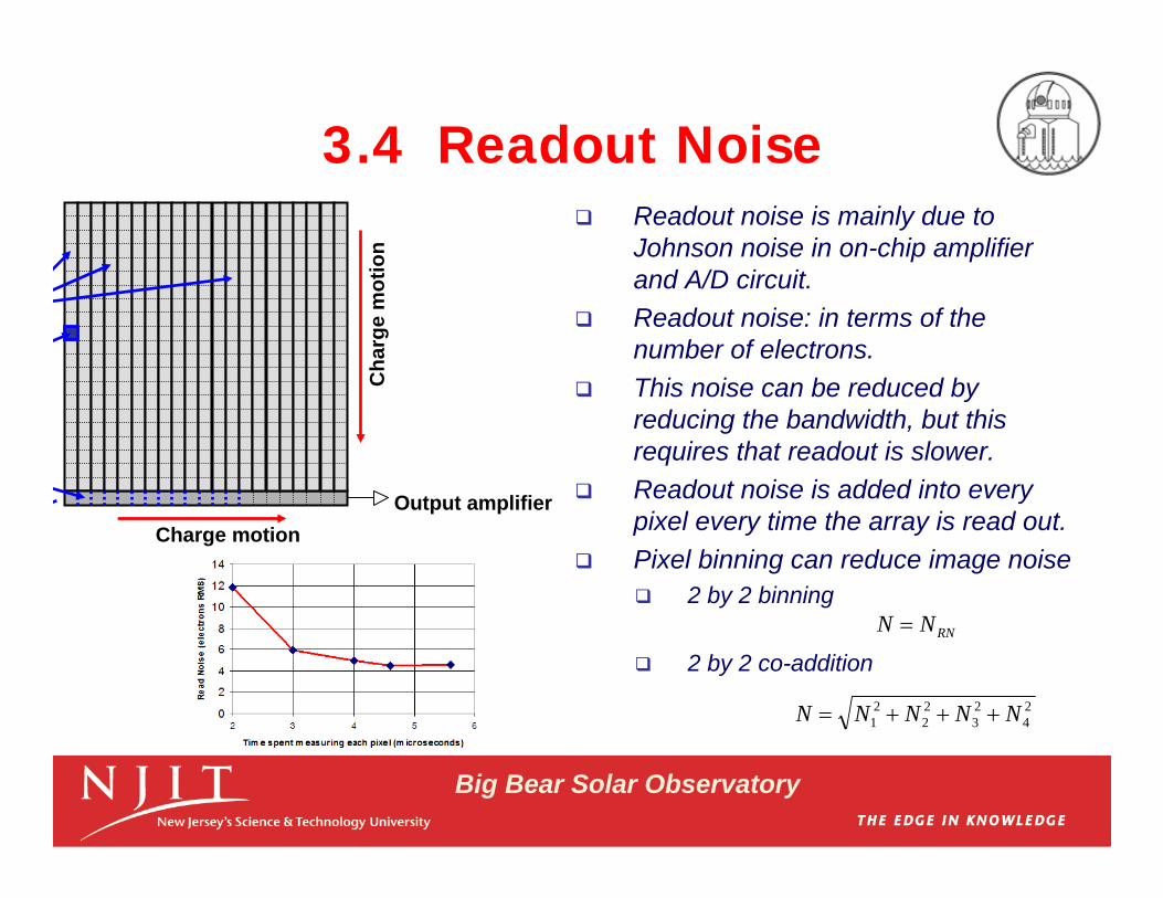
3.4 Readout Noise Readout noise is mainly due to
Johnson noise in on-chip amplifier and A/D circuit.
Readout noise: in terms of the number of electrons.
This noise can be reduced by reducing the bandwidth, but this requires that readout is slower.
Readout noise is added into every pixel every time the array is read out.
Pixel binning can reduce image noise 2 by 2 binning
2 by 2 co-addition
Charge motion
Cha
rge
mot
ion
Output amplifier
24
23
22
21 NNNNN
RNNN
Big Bear Solar Observatory
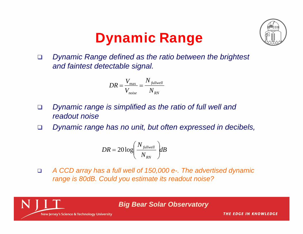
Dynamic Range Dynamic Range defined as the ratio between the brightest
and faintest detectable signal.
Dynamic range is simplified as the ratio of full well and readout noise
Dynamic range has no unit, but often expressed in decibels,
A CCD array has a full well of 150,000 e-. The advertised dynamic range is 80dB. Could you estimate its readout noise?
RN
fullwell
noise NN
VVDR max
dBN
NDR
RN
fullwell
log20
Big Bear Solar Observatory
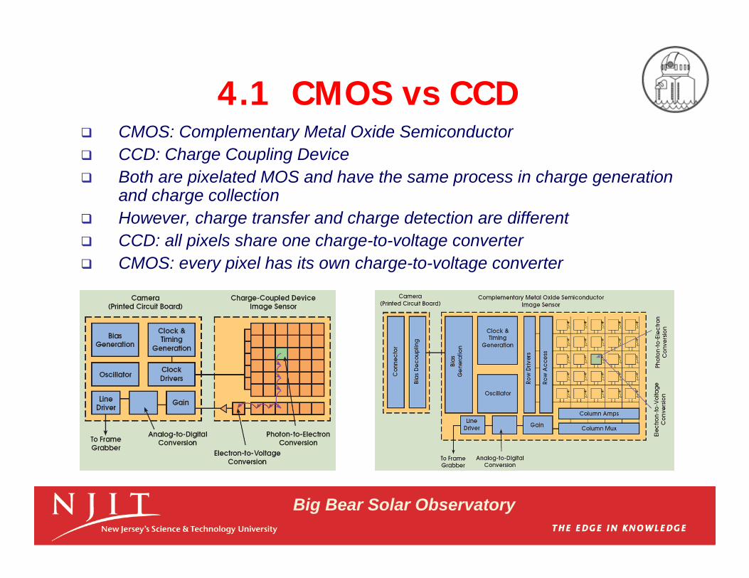
4.1 CMOS vs CCD CMOS: Complementary Metal Oxide Semiconductor CCD: Charge Coupling Device Both are pixelated MOS and have the same process in charge generation
and charge collection However, charge transfer and charge detection are different CCD: all pixels share one charge-to-voltage converter CMOS: every pixel has its own charge-to-voltage converter

Big Bear Solar Observatory
C:\Phys780_2011 Fall\Week4\CCDMovieMOD.tif
Big Bear Solar Observatory
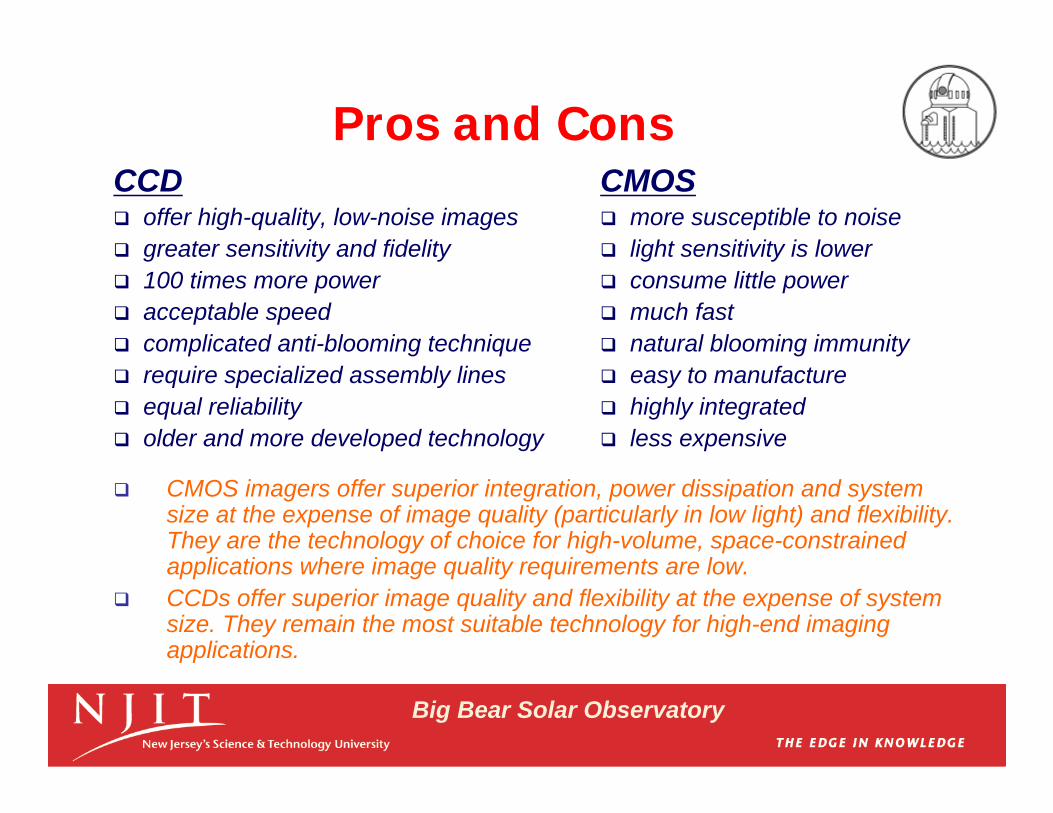
Pros and ConsCCD offer high-quality, low-noise images greater sensitivity and fidelity 100 times more power acceptable speed complicated anti-blooming technique require specialized assembly lines equal reliability older and more developed technology
CMOS more susceptible to noise light sensitivity is lower consume little power much fast natural blooming immunity easy to manufacture highly integrated less expensive
CMOS imagers offer superior integration, power dissipation and system size at the expense of image quality (particularly in low light) and flexibility. They are the technology of choice for high-volume, space-constrained applications where image quality requirements are low.
CCDs offer superior image quality and flexibility at the expense of system size. They remain the most suitable technology for high-end imaging applications.
Big Bear Solar Observatory
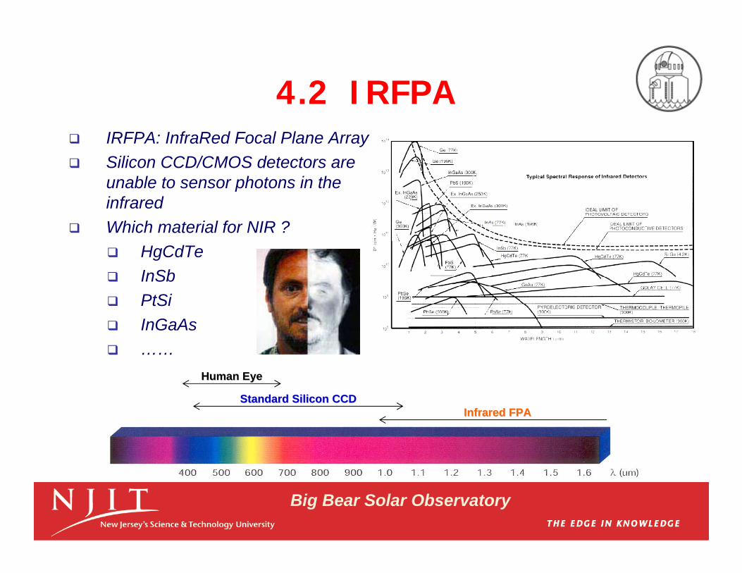
4.2 IRFPA IRFPA: InfraRed Focal Plane Array Silicon CCD/CMOS detectors are
unable to sensor photons in the infrared
Which material for NIR ? HgCdTe InSb PtSi InGaAs ……
Human EyeHuman Eye
Standard Silicon CCDStandard Silicon CCDInfrared FPAInfrared FPA
Big Bear Solar Observatory
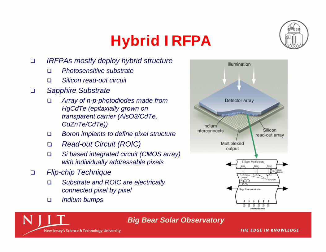
Hybrid IRFPA IRFPAs mostly deploy hybrid structure
Photosensitive substrate Silicon read-out circuit
Sapphire Substrate Array of n-p-photodiodes made from
HgCdTe (epitaxially grown on transparent carrier (AlsO3/CdTe, CdZnTe/CdTe))
Boron implants to define pixel structure Read-out Circuit (ROIC) Si based integrated circuit (CMOS array)
with individually addressable pixels Flip-chip Technique
Substrate and ROIC are electrically connected pixel by pixel
Indium bumps
Big Bear Solar Observatory
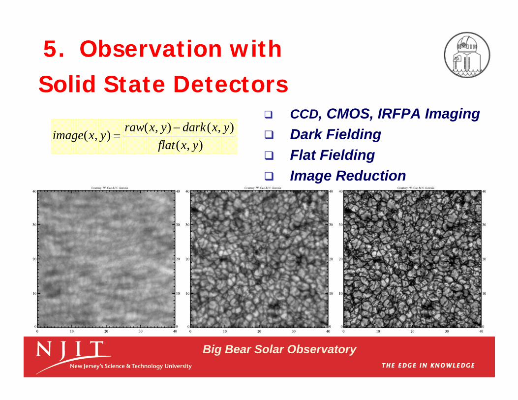
5. Observation with Solid State Detectors
CCD, CMOS, IRFPA Imaging Dark Fielding Flat Fielding Image Reduction
),(),(),(),(
yxflatyxdarkyxrawyximage