Embed Size (px)
Citation preview
Lecture 11.0Lecture 11.0
Etching
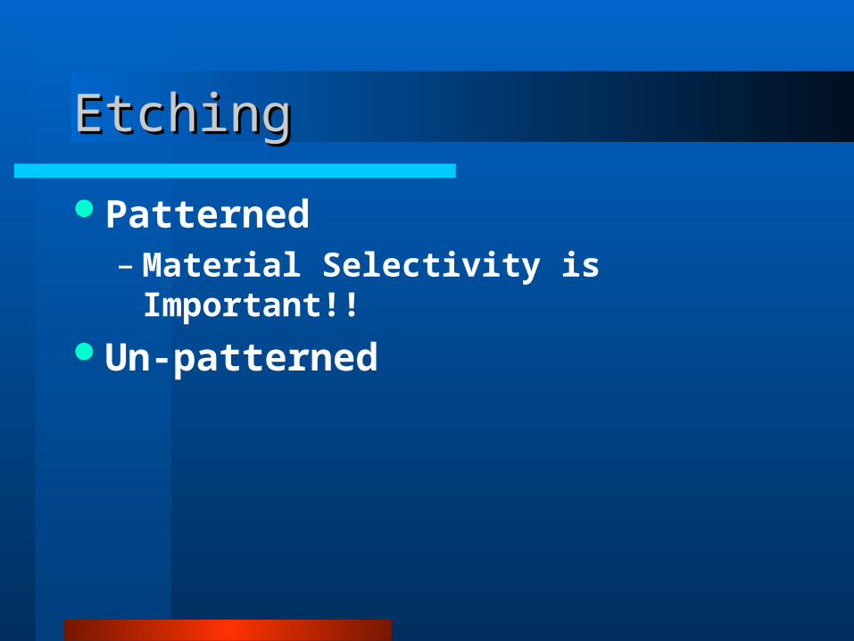
EtchingEtching
Patterned– Material Selectivity is Important!!
Un-patterned
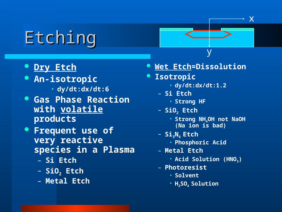
EtchingEtching
Dry Etch An-isotropic
• dy/dt:dx/dt:6
Gas Phase Reaction with volatile products
Frequent use of very reactive species in a Plasma – Si Etch– SiO2 Etch– Metal Etch
Wet Etch=Dissolution Isotropic
• dy/dt:dx/dt:1.2
– Si Etch • Strong HF
– SiO2 Etch• Strong NH4OH not NaOH (Na
ion is bad)
– Si3N4 Etch• Phosphoric Acid
– Metal Etch• Acid Solution (HNO3)
– Photoresist• Solvent• H2SO4 Solution
x
y
EtchingEtching
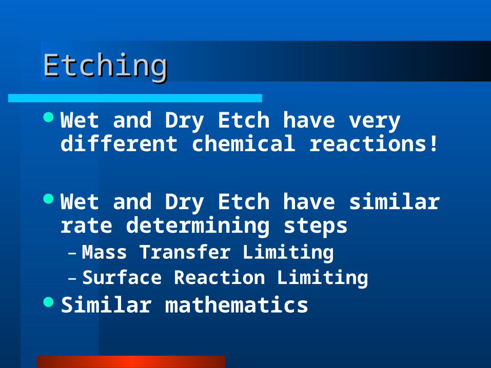
Wet and Dry Etch have very different chemical reactions!
Wet and Dry Etch have similar rate determining steps– Mass Transfer Limiting– Surface Reaction Limiting
Similar mathematics
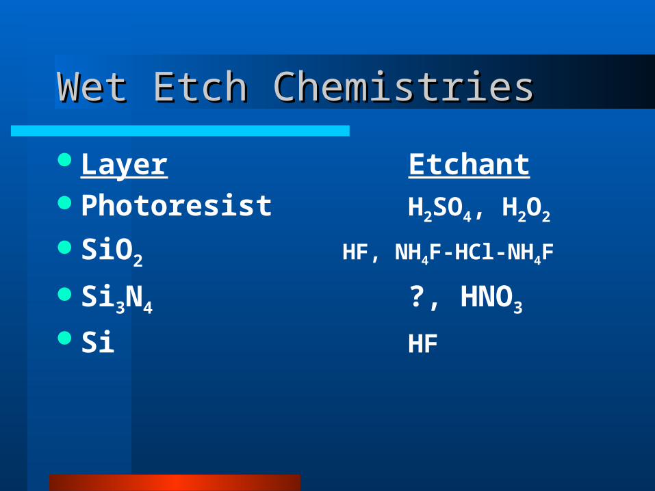
Wet Etch ChemistriesWet Etch Chemistries
Layer EtchantPhotoresist H2SO4, H2O2
SiO2 HF, NH4F-HCl-NH4F
Si3N4 ?, HNO3
Si HF
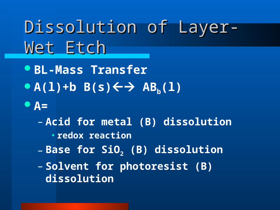
Dissolution of Layer-Wet EtchDissolution of Layer-Wet Etch
BL-Mass TransferA(l)+b B(s) ABb(l)
A=– Acid for metal (B) dissolution
• redox reaction
– Base for SiO2 (B) dissolution
– Solvent for photoresist (B) dissolution
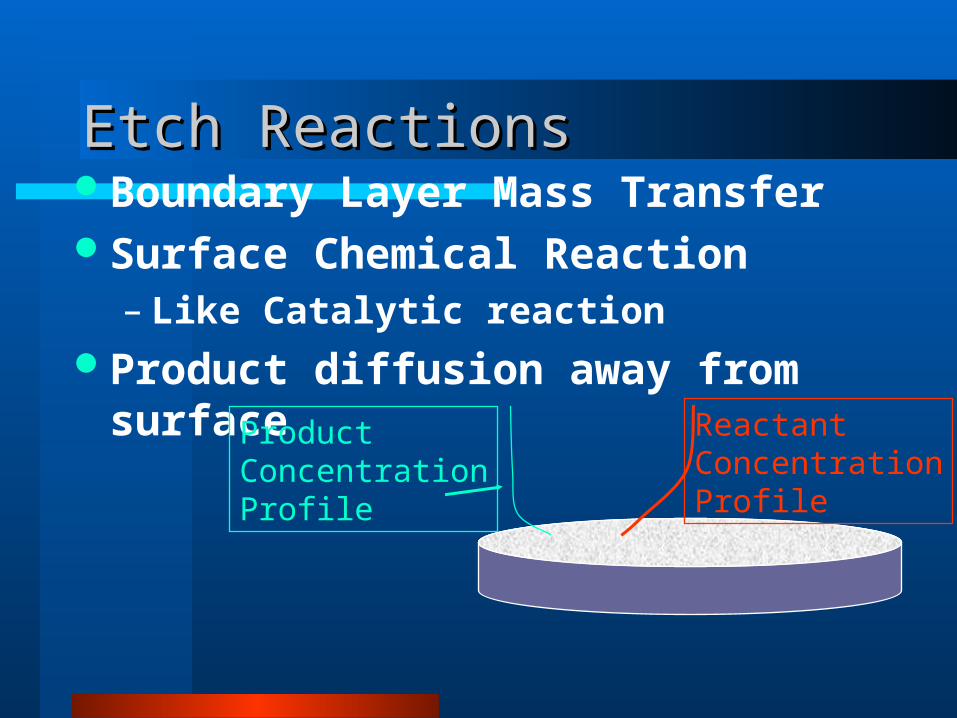
Etch ReactionsEtch ReactionsBoundary Layer Mass TransferSurface Chemical Reaction
– Like Catalytic reactionProduct diffusion away from surface
Reactant ConcentrationProfile
ProductConcentrationProfile
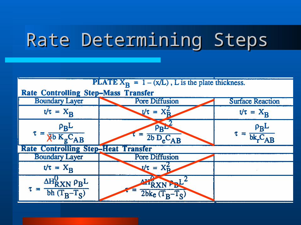
Rate Determining StepsRate Determining Steps
X
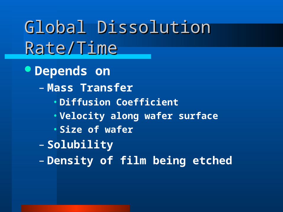
Global Dissolution Rate/TimeGlobal Dissolution Rate/Time
Depends on– Mass Transfer
• Diffusion Coefficient• Velocity along wafer surface• Size of wafer
– Solubility– Density of film being etched
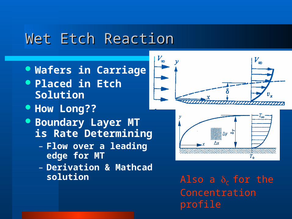
Wet Etch ReactionWet Etch Reaction
Wafers in Carriage Placed in Etch
Solution How Long?? Boundary Layer MT
is Rate Determining– Flow over a leading
edge for MT– Derivation & Mathcad
solutionAlso a C for theConcentration profile
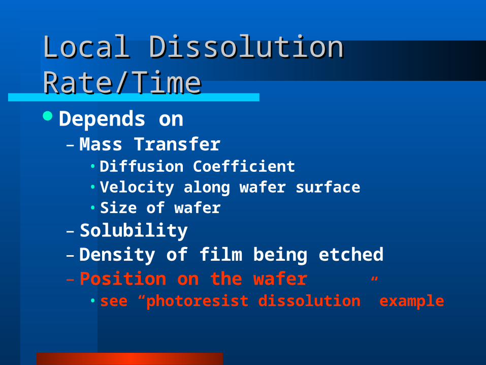
Local Dissolution Rate/TimeLocal Dissolution Rate/Time
Depends on– Mass Transfer
• Diffusion Coefficient• Velocity along wafer surface• Size of wafer
– Solubility– Density of film being etched– Position on the wafer
• see “photoresist dissolution” example
Dry EtchDry Etch
Physical Evaporation– Not typically used
• Heating chip diffuses dopants out of position
Sputtering from a targetPlasma reactor with volatile reaction
product
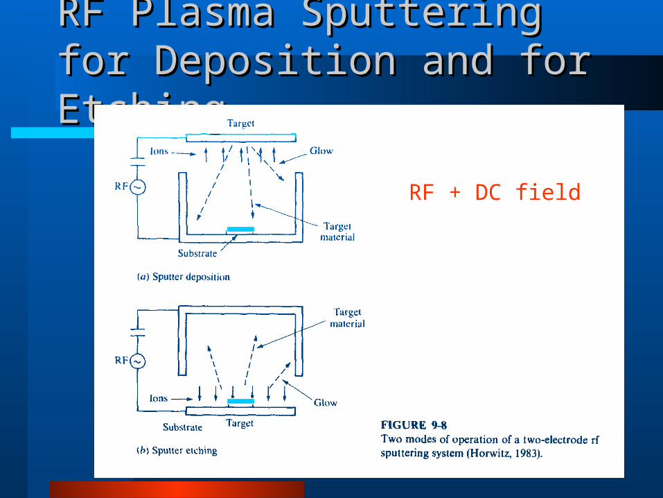
RF Plasma Sputtering for RF Plasma Sputtering for Deposition and for EtchingDeposition and for Etching
RF + DC field
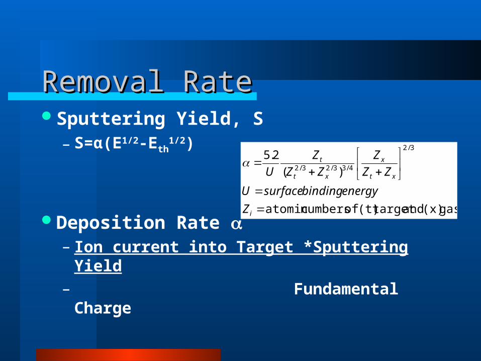
Removal RateRemoval RateSputtering Yield, S
– S=α(E1/2-Eth1/2)
Deposition Rate – Ion current into Target *Sputtering Yield– Fundamental Charge
gas(x) andtarget(t) ofnumbersatomic
)(
2.53/2
4/33/23/2
i
xt
x
xt
t
Z
energybindingsurfaceU
ZZ
Z
ZZ
Z
U
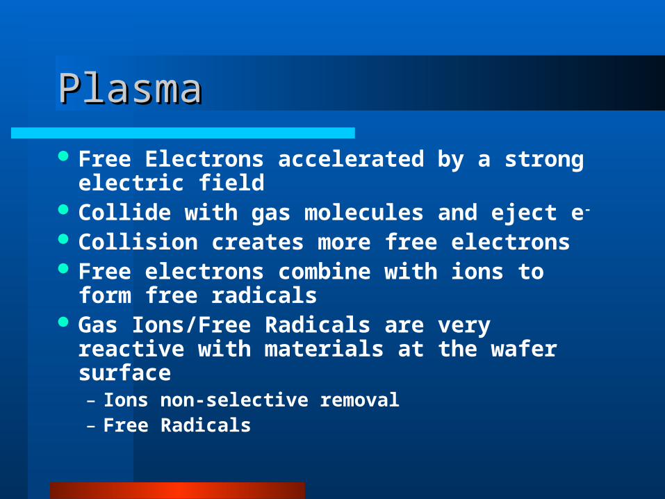
PlasmaPlasma
Free Electrons accelerated by a strong electric field
Collide with gas molecules and eject e-
Collision creates more free electrons Free electrons combine with ions to form
free radicals Gas Ions/Free Radicals are very reactive
with materials at the wafer surface– Ions non-selective removal– Free Radicals
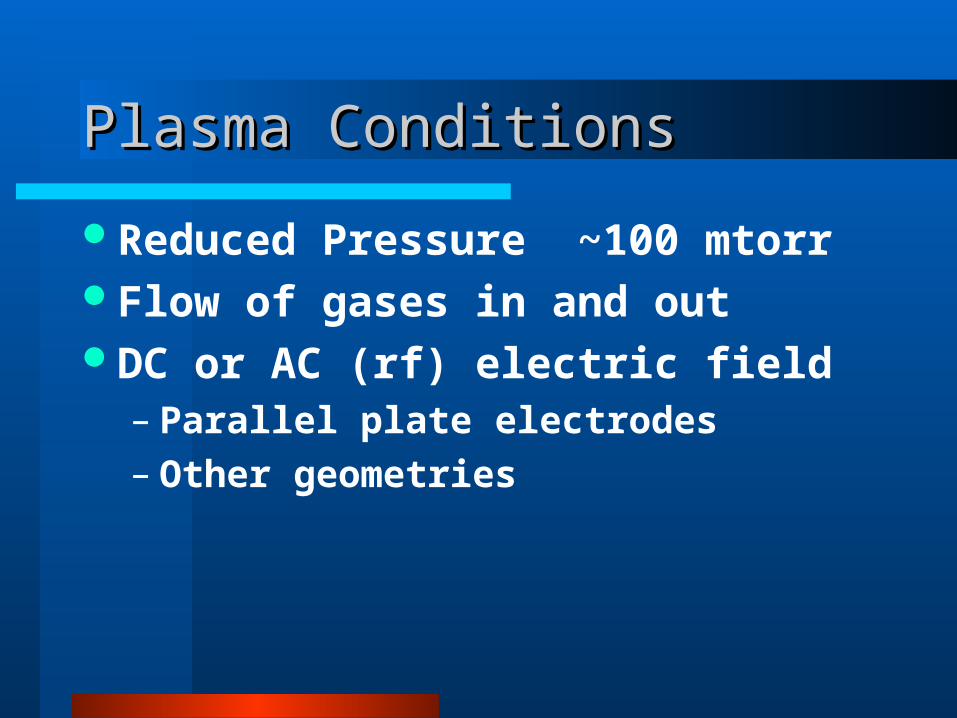
Plasma ConditionsPlasma Conditions
Reduced Pressure ~100 mtorrFlow of gases in and outDC or AC (rf) electric field
– Parallel plate electrodes– Other geometries
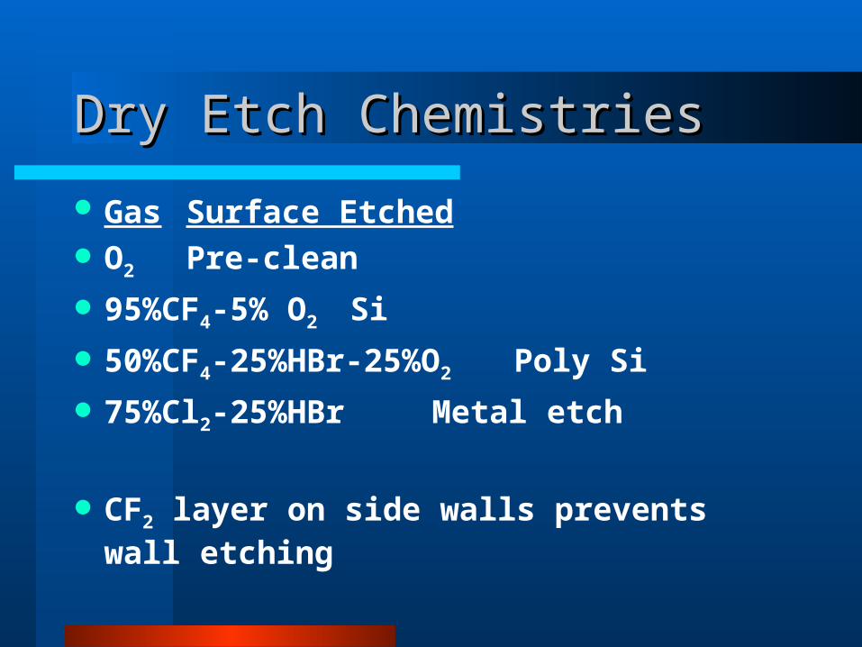
Dry Etch ChemistriesDry Etch Chemistries
Gas Surface Etched O2 Pre-clean
95%CF4-5% O2 Si
50%CF4-25%HBr-25%O2 Poly Si
75%Cl2-25%HBr Metal etch
CF2 layer on side walls prevents wall etching
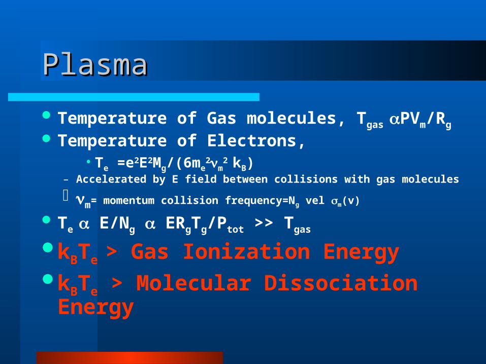
PlasmaPlasma
Temperature of Gas molecules, Tgas PVm/Rg
Temperature of Electrons, • Te =e2E2Mg/(6me
2m2 kB)
– Accelerated by E field between collisions with gas molecules
m= momentum collision frequency=Ng vel m(v)
Te E/Ng ERgTg/Ptot >> Tgas
kBTe > Gas Ionization EnergykBTe > Molecular Dissociation Energy
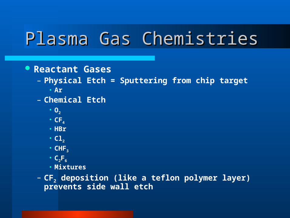
Plasma Gas ChemistriesPlasma Gas Chemistries
Reactant Gases– Physical Etch = Sputtering from chip target
• Ar
– Chemical Etch• O2
• CF4
• HBr• Cl2
• CHF3
• C2F6
• Mixtures
– CF2 deposition (like a teflon polymer layer) prevents side wall etch
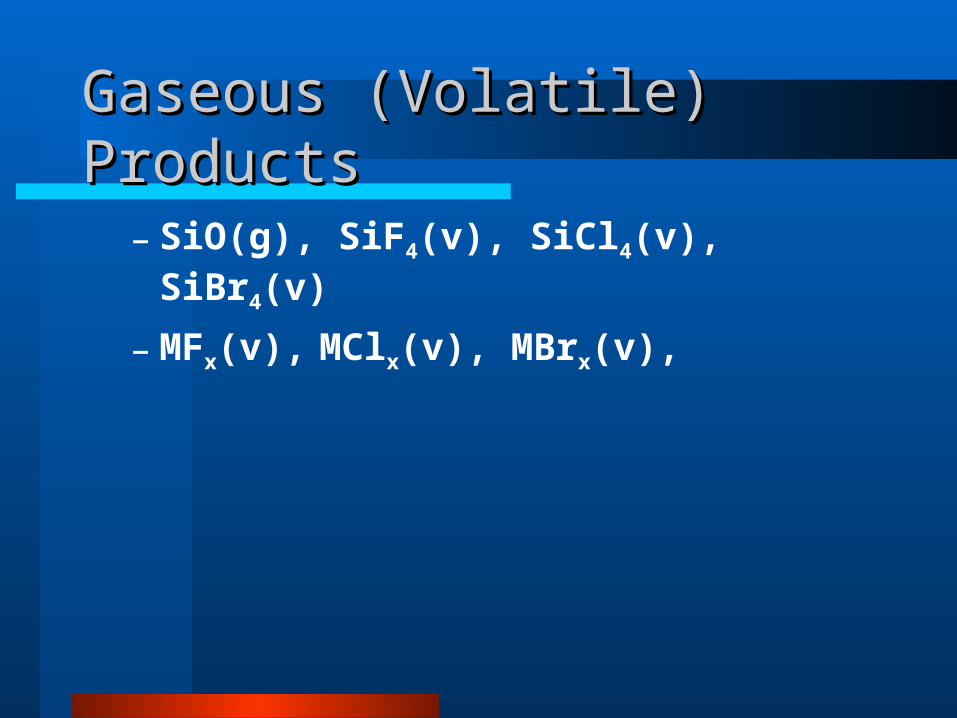
Gaseous (Volatile) ProductsGaseous (Volatile) Products
– SiO(g), SiF4(v), SiCl4(v), SiBr4(v)
– MFx(v), MClx(v), MBrx(v),
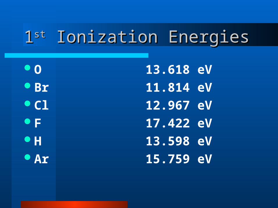
11stst Ionization Energies Ionization Energies
O 13.618 eVBr 11.814 eVCl 12.967 eVF 17.422 eVH 13.598 eVAr 15.759 eV
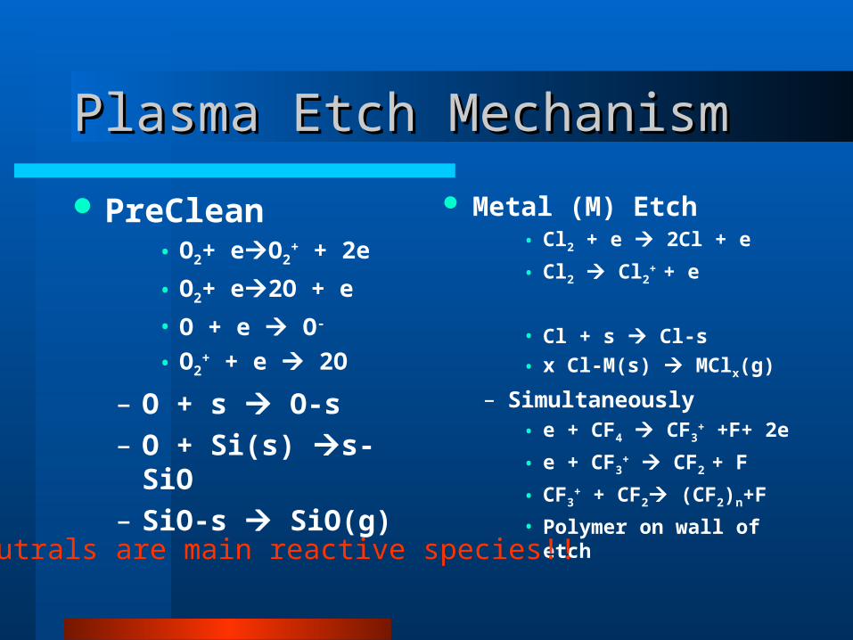
Plasma Etch MechanismPlasma Etch Mechanism
PreClean• O2+ eO2
+ + 2e
• O2+ e2O + e
• O + e O-
• O2+ + e 2O
– O + s O-s– O + Si(s) s-SiO– SiO-s SiO(g)
Metal (M) Etch• Cl2 + e 2Cl + e
• Cl2 Cl2+ + e
• Cl + s Cl-s
• x Cl-M(s) MClx(g)
– Simultaneously• e + CF4 CF3
+ +F+ 2e
• e + CF3+ CF2 + F
• CF3+ + CF2 (CF2)n+F
• Polymer on wall of etchNeutrals are main reactive species!!
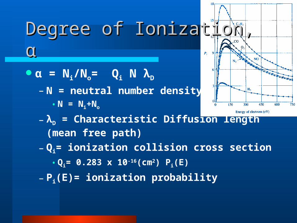
Degree of Ionization, Degree of Ionization, α α
α = Ni/No= Qi N λD
– N = neutral number density • N = Ni+No
– λD = Characteristic Diffusion length (mean free path)
– Qi= ionization collision cross section
• Qi= 0.283 x 10⁻¹⁶(cm2) Pi(E)
– Pi(E)= ionization probability
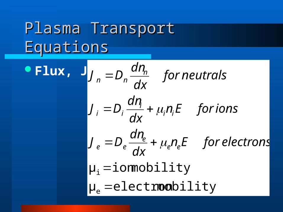
Plasma Transport EquationsPlasma Transport Equations
Flux, J
mobilityelectronμ
mobilityionμ
e
i
electronsforEndx
dnDJ
ionsforEndx
dnDJ
neutralsfordx
dnDJ
eee
ee
iii
ii
nnn

Etch ReactionsEtch ReactionsBoundary Layer Mass TransferSurface Chemical Reaction
– Like Catalytic reactionProduct diffusion away from surface
Reactant ConcentrationProfile
ProductConcentrationProfile
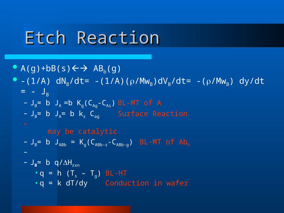
Etch ReactionEtch Reaction
A(g)+bB(s) ABb(g) -(1/A) dNB/dt= -(1/A)(/MwB)dVB/dt= -(/MwB) dy/dt = - JB
– JB= b JA =b Kg(CAg-CAs) BL-MT of A– JB= b JA= b ks Cag Surface Reaction– may be catalytic– JB= b JABb = Kg(CABb-s-CABb-g)BL-MT of Abb
–
– JB= b q/Hrxn
• q = h (Ts – Tg) BL-HT• q = k dT/dy Conduction in wafer
Rate Determining StepsRate Determining Steps
X
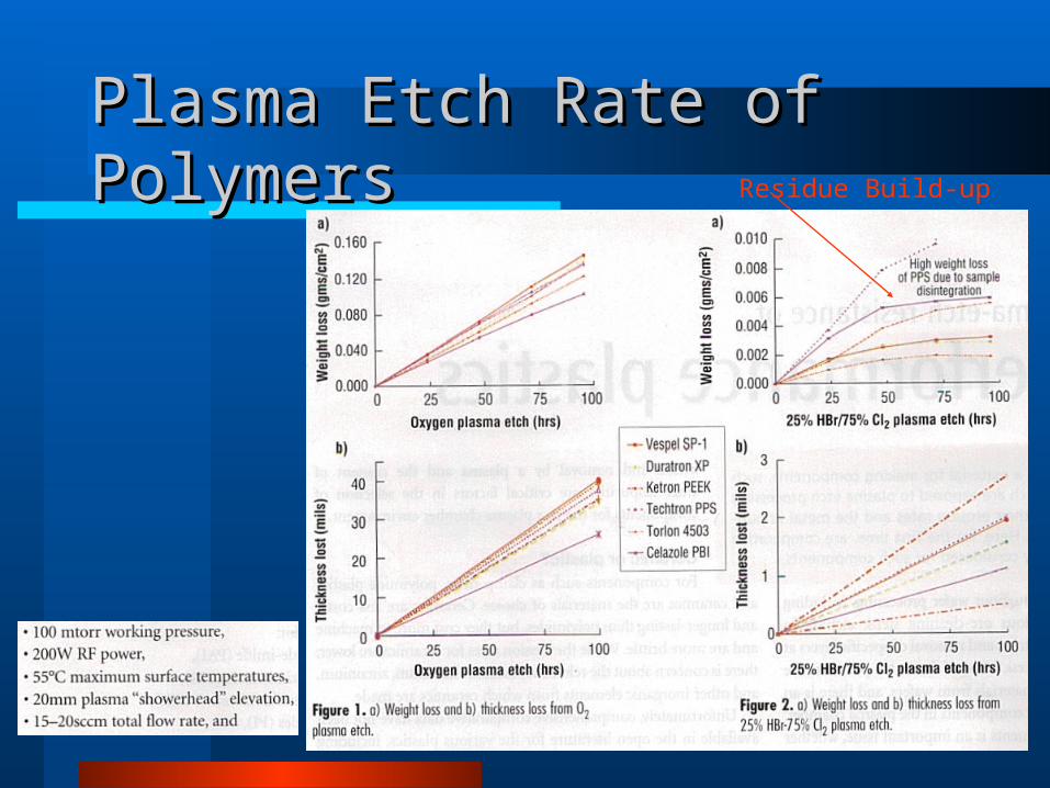
Plasma Etch Rate of PolymersPlasma Etch Rate of PolymersResidue Build-up
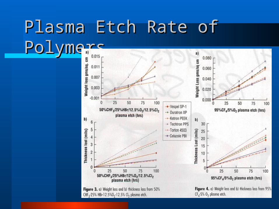
Plasma Etch Rate of PolymersPlasma Etch Rate of Polymers
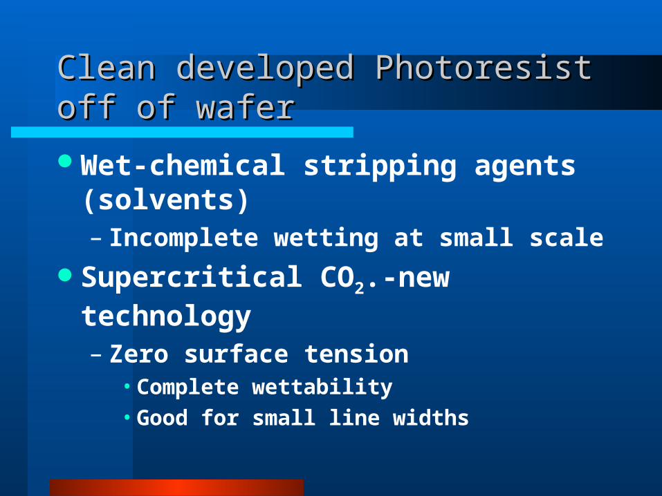
Clean developed Photoresist off of waferClean developed Photoresist off of wafer
Wet-chemical stripping agents (solvents)– Incomplete wetting at small scale
Supercritical CO2.-new technology
– Zero surface tension• Complete wettability• Good for small line widths
![Reactive ion etching. Material selectivity Ion Beam milling @INESC Nordiko 3000 IBD system Etch rates [Å/min] @ 70ºpan 65 W130 W * junctions, spin valves](https://img.pdfslide.net/doc/110x75/56649d575503460f94a3545a/reactive-ion-etching-material-selectivity-ion-beam-milling-inesc-nordiko.jpg)


![FIB Secondary Etching Method for Fabrication of Fine CNT ... · laser etching method was utilized to obtain microstructures of CNT brushes [21]. Moreover, the patterned growth of](https://img.pdfslide.net/doc/110x75/5e7104f042569253791c508c/fib-secondary-etching-method-for-fabrication-of-fine-cnt-laser-etching-method.jpg)


![Etching of 42 nm and 32 nm Half-Pitch Features Patterned ...cnt.canon.com/wp-content/uploads/2014/07/SPIE-2008-etch-study.pdf · [Figure 1]. The authors demonstrate control of CDs,](https://img.pdfslide.net/doc/110x75/5eba3308912d953f6d5f60de/etching-of-42-nm-and-32-nm-half-pitch-features-patterned-cntcanoncomwp-contentuploads201407spie-2008-etch-studypdf.jpg)