Embed Size (px)
Citation preview
Lecture 16 –Introduction to Optical Lithography
EECS 598-002 Winter 2006Nanophotonics and Nano-scale Fabrication
P.C.Ku
2EECS 598-002 Nanophotonics and Nanoscale Fabrication by P.C.Ku
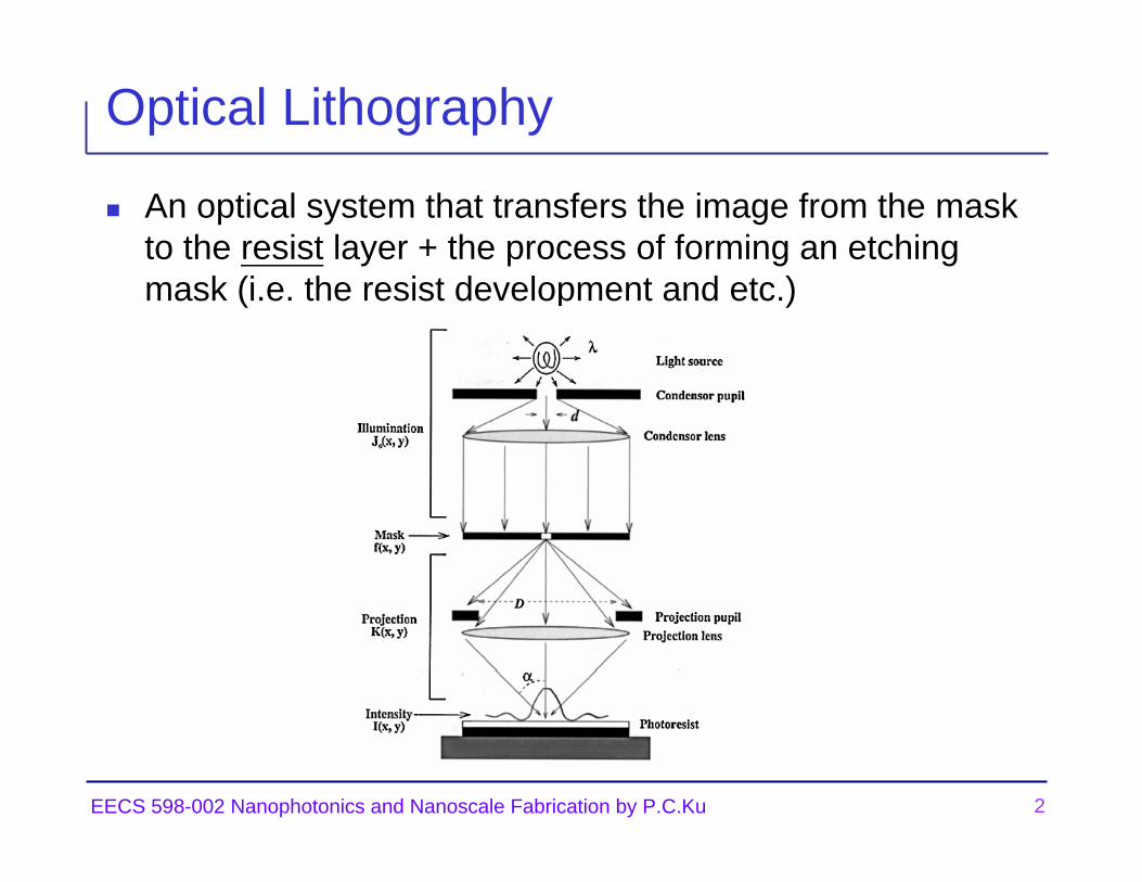
Optical Lithography
An optical system that transfers the image from the mask to the resist layer + the process of forming an etching mask (i.e. the resist development and etc.)
3EECS 598-002 Nanophotonics and Nanoscale Fabrication by P.C.Ku
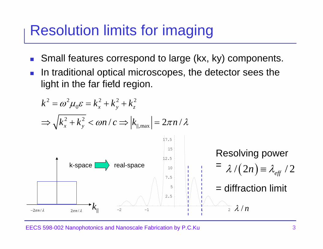
Resolution limits for imaging
Small features correspond to large (kx, ky) components.In traditional optical microscopes, the detector sees the light in the far field region.
2 2 2 2 20
2 2,max/ 2 /
x y z
x y
k k k k
k k n c k n
ω µ ε
ω π λ
= = + +
⇒ + < ⇒ =
-2 -1 1 2
2.5
5
7.5
10
12.5
15
17.5
k
2 /nπ λ2 /nπ λ− k
Resolving power=
= diffraction limit
/ nλ
( )/ 2 / 2effnλ λ≡real-spacek-space
4EECS 598-002 Nanophotonics and Nanoscale Fabrication by P.C.Ku
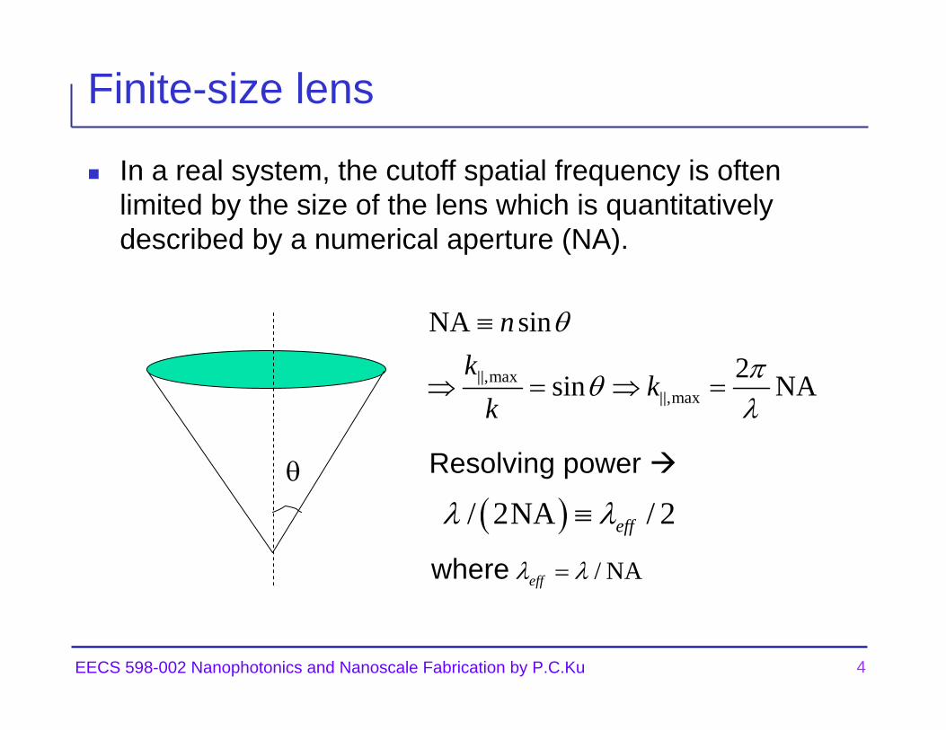
Finite-size lens
In a real system, the cutoff spatial frequency is often limited by the size of the lens which is quantitatively described by a numerical aperture (NA).
θ
,max,max
NA sin2sin NA
nk
kk
θπθλ
≡
⇒ = ⇒ =
Resolving power
( )/ 2NA / 2effλ λ≡
where / NAeffλ λ=
5EECS 598-002 Nanophotonics and Nanoscale Fabrication by P.C.Ku
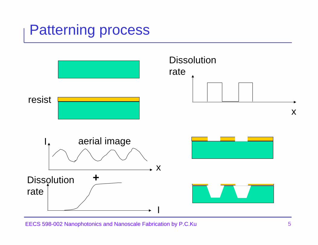
Patterning process
resist
x
I aerial image
+
I
Dissolutionrate
Dissolutionrate
x
6EECS 598-002 Nanophotonics and Nanoscale Fabrication by P.C.Ku
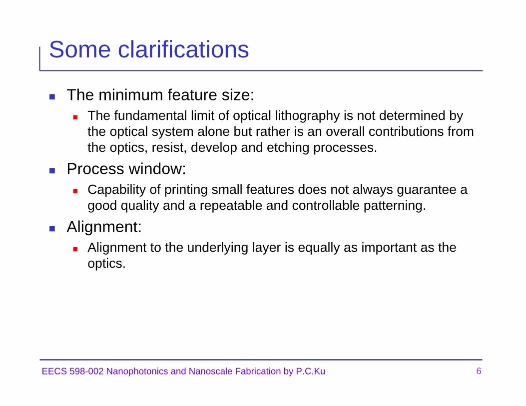
Some clarifications
The minimum feature size:The fundamental limit of optical lithography is not determined by the optical system alone but rather is an overall contributions from the optics, resist, develop and etching processes.
Process window:Capability of printing small features does not always guarantee a good quality and a repeatable and controllable patterning.
Alignment:Alignment to the underlying layer is equally as important as theoptics.
7EECS 598-002 Nanophotonics and Nanoscale Fabrication by P.C.Ku
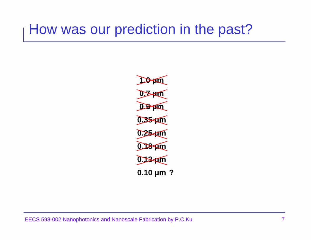
How was our prediction in the past?
1.0 µm0.7 µm0.5 µm0.35 µm0.25 µm0.18 µm0.13 µm0.10 µm ?
8EECS 598-002 Nanophotonics and Nanoscale Fabrication by P.C.Ku
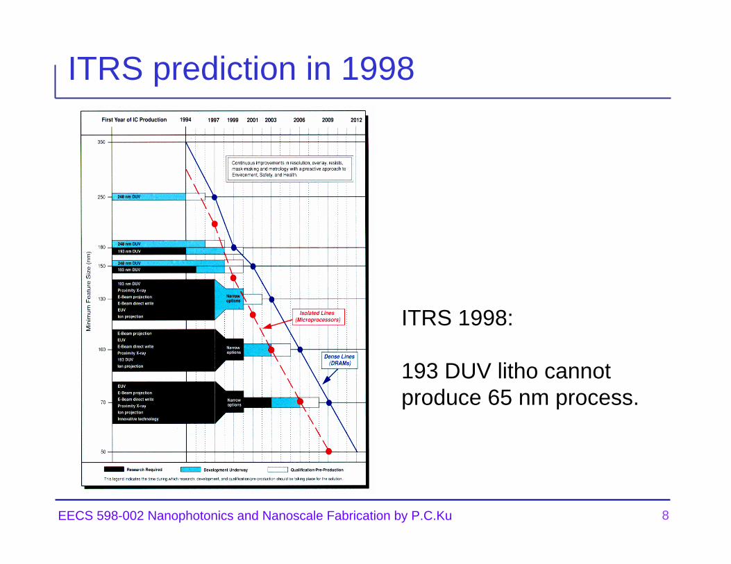
ITRS prediction in 1998
ITRS 1998:
193 DUV litho cannotproduce 65 nm process.
9EECS 598-002 Nanophotonics and Nanoscale Fabrication by P.C.Ku
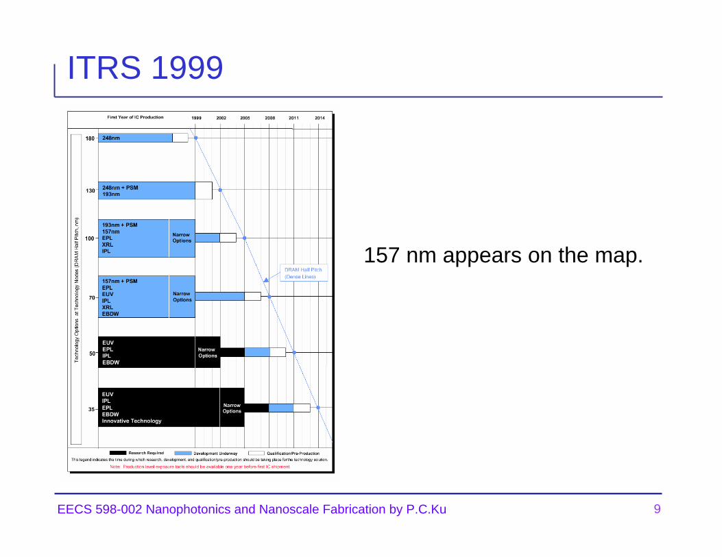
ITRS 1999
157 nm appears on the map.
10EECS 598-002 Nanophotonics and Nanoscale Fabrication by P.C.Ku
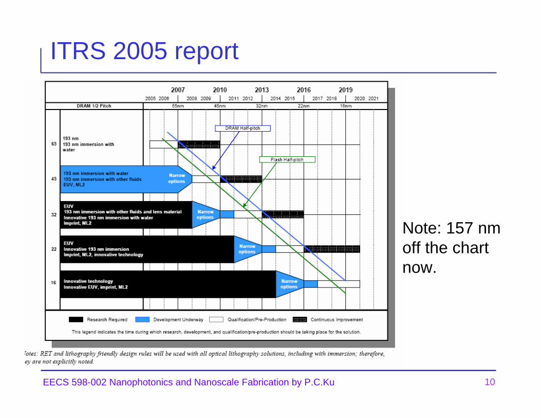
ITRS 2005 report
Note: 157 nmoff the chartnow.
11EECS 598-002 Nanophotonics and Nanoscale Fabrication by P.C.Ku
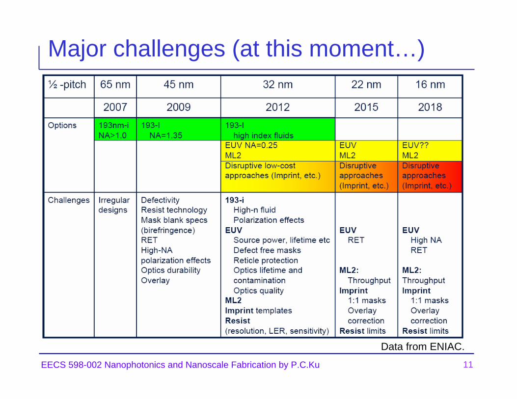
Major challenges (at this moment…)
Data from ENIAC.
12EECS 598-002 Nanophotonics and Nanoscale Fabrication by P.C.Ku
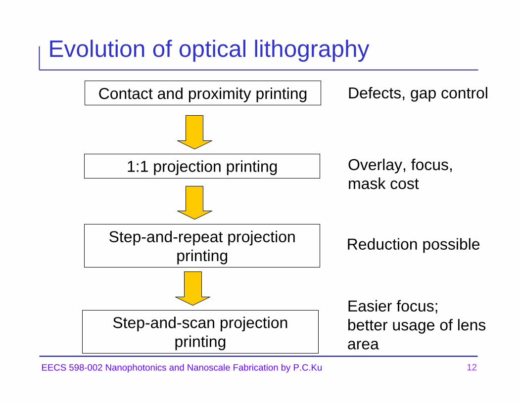
Evolution of optical lithography
Contact and proximity printing
1:1 projection printing
Step-and-repeat projection printing
Step-and-scan projection printing
Defects, gap control
Overlay, focus,mask cost
Reduction possible
Easier focus;better usage of lensarea
13EECS 598-002 Nanophotonics and Nanoscale Fabrication by P.C.Ku
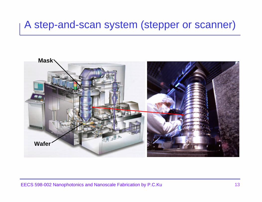
A step-and-scan system (stepper or scanner)
Wafer
Mask
14EECS 598-002 Nanophotonics and Nanoscale Fabrication by P.C.Ku
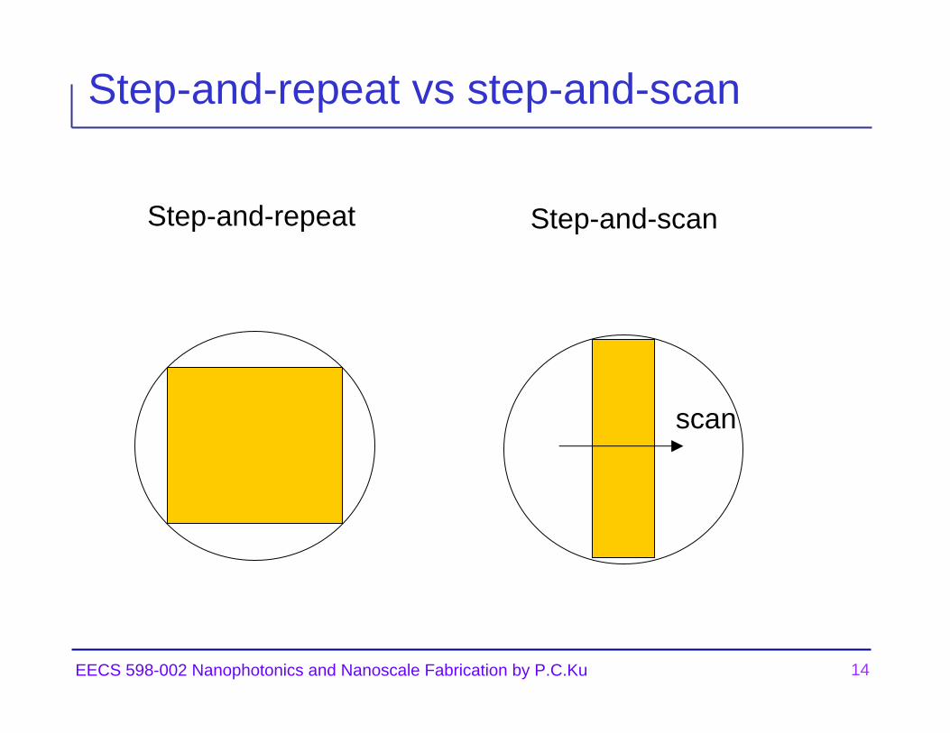
Step-and-repeat vs step-and-scan
Step-and-repeat Step-and-scan
scan
15EECS 598-002 Nanophotonics and Nanoscale Fabrication by P.C.Ku
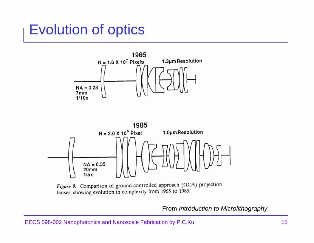
Evolution of optics
From Introduction to Microlithography
16EECS 598-002 Nanophotonics and Nanoscale Fabrication by P.C.Ku
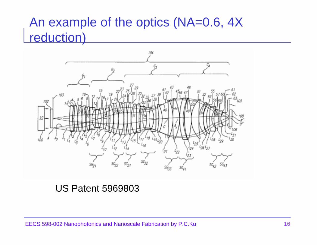
An example of the optics (NA=0.6, 4X reduction)
US Patent 5969803
17EECS 598-002 Nanophotonics and Nanoscale Fabrication by P.C.Ku
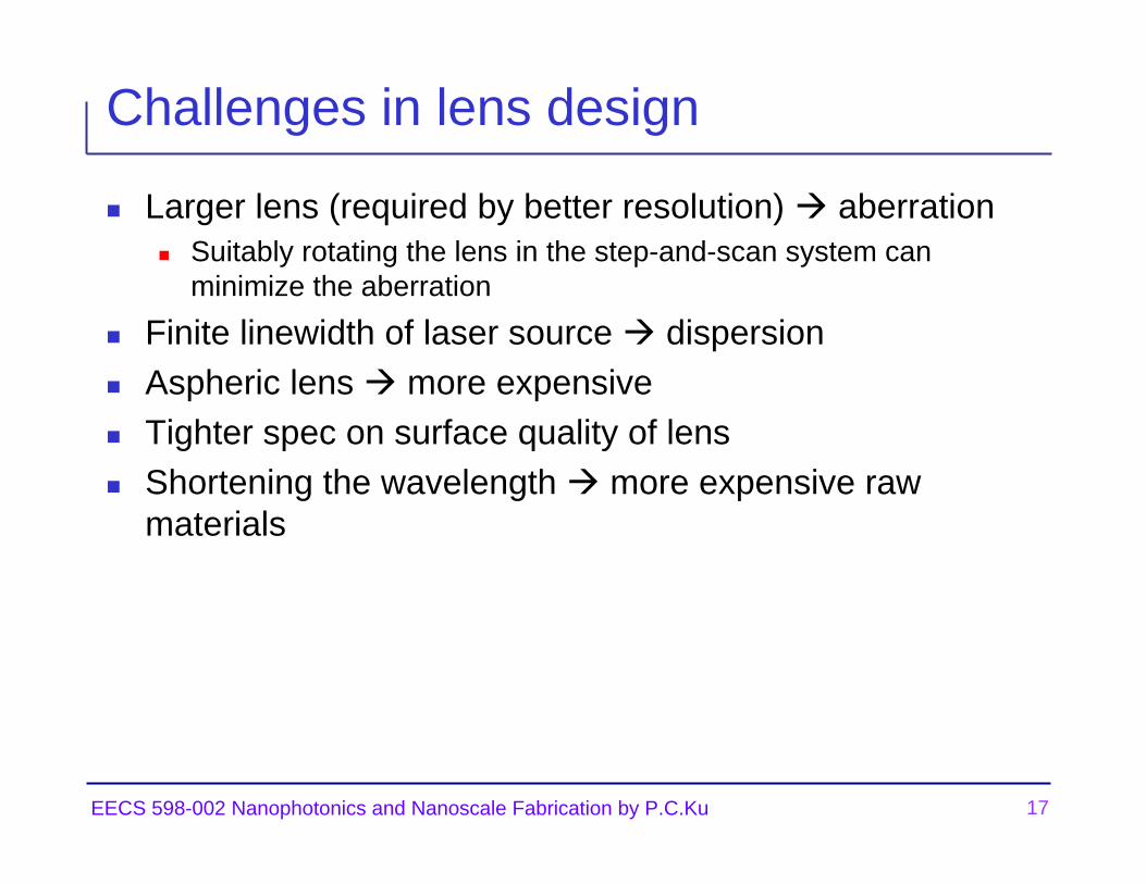
Challenges in lens design
Larger lens (required by better resolution) aberrationSuitably rotating the lens in the step-and-scan system can minimize the aberration
Finite linewidth of laser source dispersionAspheric lens more expensiveTighter spec on surface quality of lensShortening the wavelength more expensive raw materials
18EECS 598-002 Nanophotonics and Nanoscale Fabrication by P.C.Ku
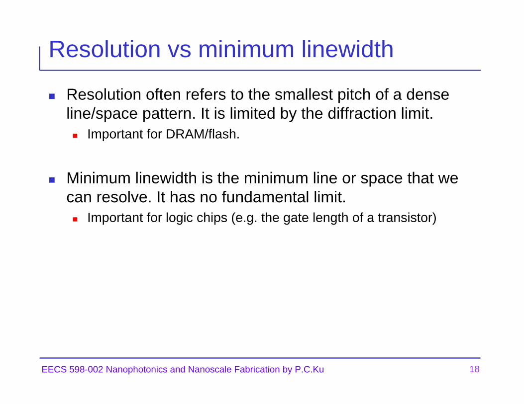
Resolution vs minimum linewidth
Resolution often refers to the smallest pitch of a dense line/space pattern. It is limited by the diffraction limit.
Important for DRAM/flash.
Minimum linewidth is the minimum line or space that we can resolve. It has no fundamental limit.
Important for logic chips (e.g. the gate length of a transistor)
19EECS 598-002 Nanophotonics and Nanoscale Fabrication by P.C.Ku
There’s no fundamental limit to optical lithography!
20EECS 598-002 Nanophotonics and Nanoscale Fabrication by P.C.Ku
Fundamentals of lithographic optics
DiffractionPartial coherenceDepth of focusReflection and interferencePolarization dependence
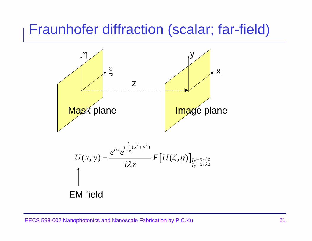
21EECS 598-002 Nanophotonics and Nanoscale Fabrication by P.C.Ku
Fraunhofer diffraction (scalar; far-field)
[ ]2 2( )
2
//
( , ) ( , ) xy
ki x yikz z
f x zf x z
e eU x y F Ui z
λλ
ξ ηλ
+
==
=
ξ
η
Mask plane
x
y
Image plane
EM field
z
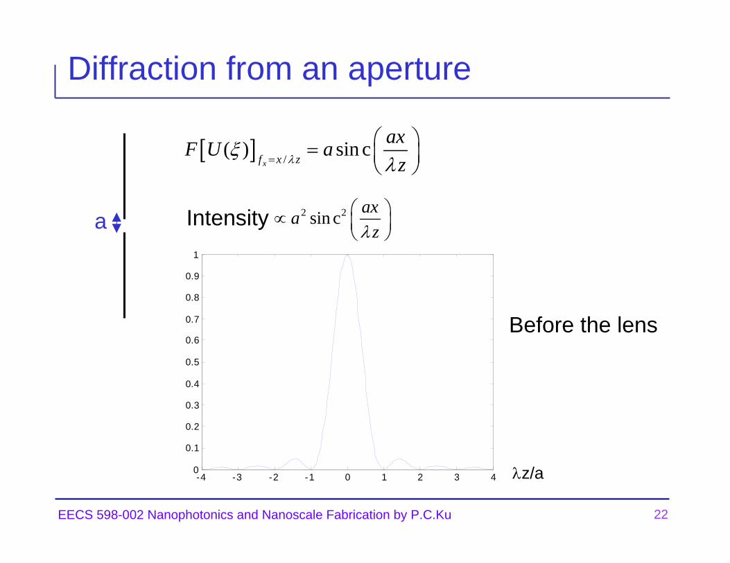
22EECS 598-002 Nanophotonics and Nanoscale Fabrication by P.C.Ku
Diffraction from an aperture
[ ] /( ) sin cxf x z
axF U azλ
ξλ=
⎛ ⎞= ⎜ ⎟⎝ ⎠
a Intensity 2 2sin c axazλ
⎛ ⎞∝ ⎜ ⎟⎝ ⎠
-4 -3 -2 -1 0 1 2 3 40
0.1
0.2
0.3
0.4
0.5
0.6
0.7
0.8
0.9
1
λz/a
Before the lens
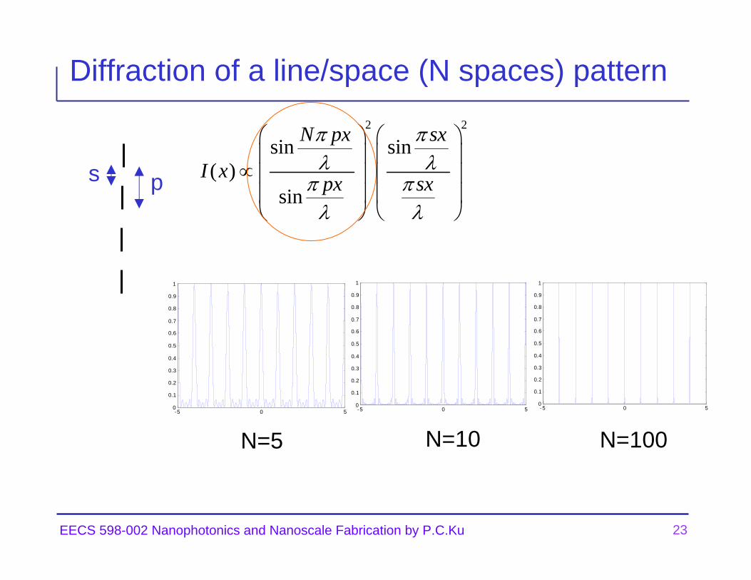
23EECS 598-002 Nanophotonics and Nanoscale Fabrication by P.C.Ku
Diffraction of a line/space (N spaces) pattern
ps
2 2
sin sin( )
sin
N px sx
I x px sx
π πλ λ
π πλ λ
⎛ ⎞ ⎛ ⎞⎜ ⎟ ⎜ ⎟
∝ ⎜ ⎟ ⎜ ⎟⎜ ⎟ ⎜ ⎟⎝ ⎠ ⎝ ⎠
-5 0 50
0.1
0.2
0.3
0.4
0.5
0.6
0.7
0.8
0.9
1
-5 0 50
0.1
0.2
0.3
0.4
0.5
0.6
0.7
0.8
0.9
1
-5 0 50
0.1
0.2
0.3
0.4
0.5
0.6
0.7
0.8
0.9
1
N=5 N=10 N=100
24EECS 598-002 Nanophotonics and Nanoscale Fabrication by P.C.Ku
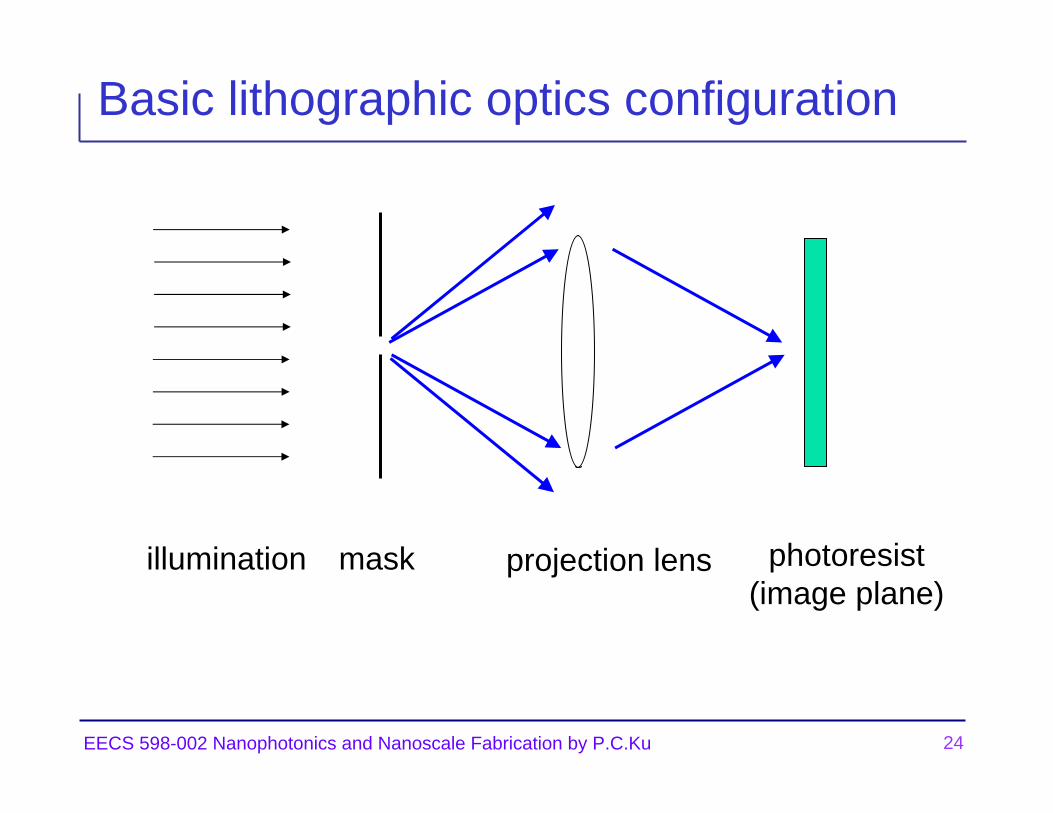
Basic lithographic optics configuration
maskillumination projection lens photoresist(image plane)
25EECS 598-002 Nanophotonics and Nanoscale Fabrication by P.C.Ku
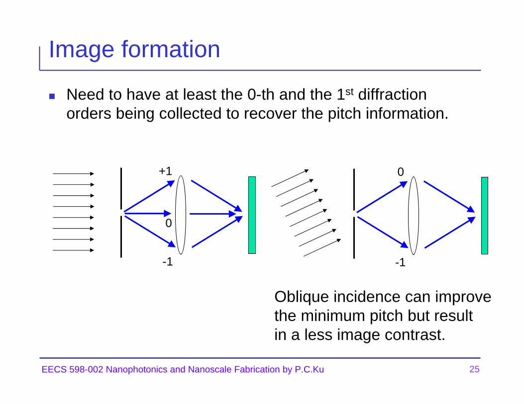
Image formation
Need to have at least the 0-th and the 1st diffraction orders being collected to recover the pitch information.
+1
-1
0
0
-1
Oblique incidence can improvethe minimum pitch but resultin a less image contrast.