Embed Size (px)
DESCRIPTION
LG FLATRON Monitor W1752T Service Manual
Citation preview
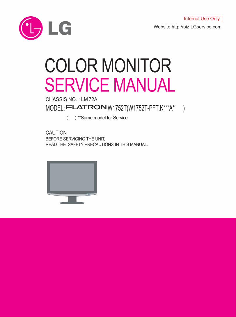
COLOR MONITORSERVICE MANUAL
Website:http://biz.LGservice.com
CAUTIONBEFORE SERVICING THE UNIT, READ THE SAFETY PRECAUTIONS IN THIS MANUAL.
CHASSIS NO. : LM 72A
MODEL: W1752T(W1752T-PFT.K***A** )( ) **Same model for Service
Internal Use Only
- 2 -Copyright 2007 LG Electronics. Inc. All right reserved.Only for training and service purposes
LGE Internal Use Only
CONTENTS
SPECIFICATIONS ................................................... 2
PRECAUTIONS ....................................................... 4
TIMING CHART ....................................................... 8
DISASSEMBLY ........................................................ 9
BLOCK DIAGRAM ................................................. 10
DESCRIPTION OF BLOCK DIAGRAM...................11
ADJUSTMENT ...................................................... 13
TROUBLESHOOTING GUIDE .............................. 15
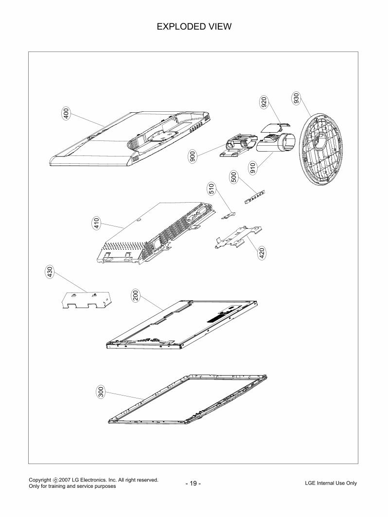
EXPLODED VIEW...................................................19
REPLACEMENT PARTS LIST ...............................21
SCHEMATIC DIAGRAM......................................... 23
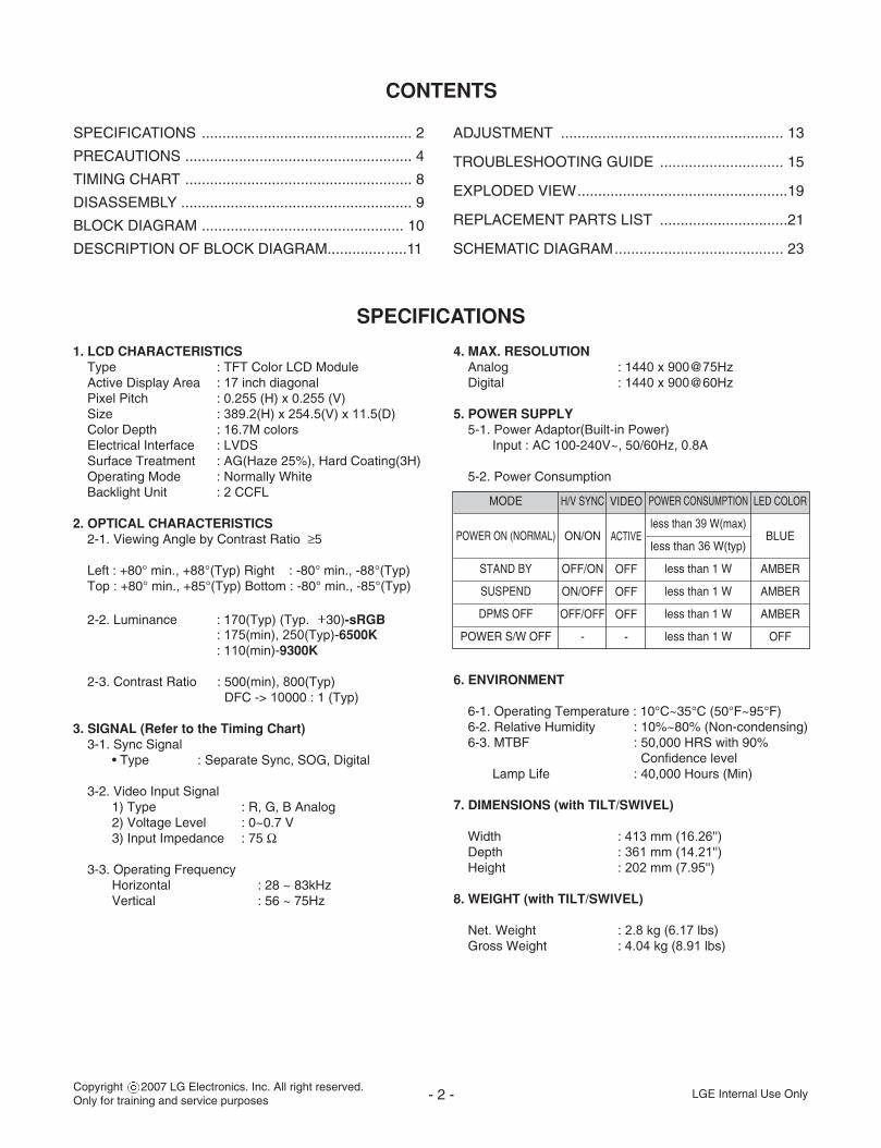
1. LCD CHARACTERISTICSType : TFT Color LCD ModuleActive Display Area : 17 inch diagonalPixel Pitch : 0.255 (H) x 0.255 (V)Size : 389.2(H) x 254.5(V) x 11.5(D)Color Depth : 16.7M colorsElectrical Interface : LVDSSurface Treatment : AG(Haze 25%), Hard Coating(3H) Operating Mode : Normally WhiteBacklight Unit : 2 CCFL
2. OPTICAL CHARACTERISTICS2-1. Viewing Angle by Contrast Ratio ≥5
Left : +80° min., +88°(Typ) Right : -80° min., -88°(Typ)Top : +80° min., +85°(Typ) Bottom : -80° min., -85°(Typ)
2-2. Luminance : 170(Typ) (Typ. 30)-sRGB: 175(min), 250(Typ)-6500K: 110(min)-9300K
2-3. Contrast Ratio : 500(min), 800(Typ)DFC -> 10000 : 1 (Typ)
3. SIGNAL (Refer to the Timing Chart)3-1. Sync Signal
• Type : Separate Sync, SOG, Digital
3-2. Video Input Signal1) Type : R, G, B Analog2) Voltage Level : 0~0.7 V3) Input Impedance : 75 Ω
3-3. Operating FrequencyHorizontal : 28 ~ 83kHzVertical : 56 ~ 75Hz
4. MAX. RESOLUTIONAnalog : 1440 x 900@75HzDigital : 1440 x 900@60Hz
5. POWER SUPPLY5-1. Power Adaptor(Built-in Power)
Input : AC 100-240V~, 50/60Hz, 0.8A
5-2. Power Consumption
6. ENVIRONMENT
6-1. Operating Temperature : 10°C~35°C (50°F~95°F)6-2. Relative Humidity : 10%~80% (Non-condensing)6-3. MTBF : 50,000 HRS with 90%
Confidence levelLamp Life : 40,000 Hours (Min)
7. DIMENSIONS (with TILT/SWIVEL)
Width : 413 mm (16.26'')Depth : 361 mm (14.21'')Height : 202 mm (7.95'')
8. WEIGHT (with TILT/SWIVEL)
Net. Weight : 2.8 kg (6.17 lbs)Gross Weight : 4.04 kg (8.91 lbs)
SPECIFICATIONS
MODE
POWER ON (NORMAL)
STAND BY
SUSPEND
DPMS OFF
POWER S/W OFF
H/V SYNC
ON/ON
OFF/ON
ON/OFF
OFF/OFF
-
POWER CONSUMPTION
less than 39 W(max)
less than 36 W(typ)
less than 1 W
less than 1 W
less than 1 W
less than 1 W
LED COLOR
BLUE
AMBER
AMBER
AMBER
OFF
VIDEO
ACTIVE
OFF
OFF
OFF
-
- 3 -Copyright 2007 LG Electronics. Inc. All right reserved.Only for training and service purposes
LGE Internal Use Only
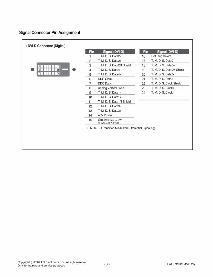
Signal Connector Pin Assignment
Pin Signal (DVI-D)123456789101112131415
T. M. D. S. Data2-T. M. D. S. Data2+T. M. D. S. Data2/4 ShieldT. M. D. S. Data4-T. M. D. S. Data4+DDC ClockDDC DataAnalog Vertical Sync.T. M. D. S. Data1-T. M. D. S. Data1+T. M. D. S. Data1/3 ShieldT. M. D. S. Data3-T. M. D. S. Data3++5V PowerGround (return for +5V, H. Sync. and V. Sync.)
Pin Signal (DVI-D)
1 89
17 2416
161718192021222324
Hot Plug DetectT. M. D. S. Data0-T. M. D. S. Data0+T. M. D. S. Data0/5 ShieldT. M. D. S. Data5-T. M. D. S. Data5+T. M. D. S. Clock ShieldT. M. D. S. Clock+T. M. D. S. Clock-
T. M. D. S. (Transition Minimized Differential Signaling)
• DVI-D Connector (Digital)
- 4 -Copyright 2007 LG Electronics. Inc. All right reserved.Only for training and service purposes
LGE Internal Use Only
WARNING FOR THE SAFETY-RELATED COMPONENT.
• There are some special components used in LCDmonitor that are important for safety. These parts aremarked on the schematic diagram and thereplacement parts list. It is essential that these criticalparts should be replaced with the manufacturer’sspecified parts to prevent electric shock, fire or otherhazard.
• Do not modify original design without obtaining writtenpermission from manufacturer or you will void theoriginal parts and labor guarantee.
TAKE CARE DURING HANDLING THE LCD MODULEWITH BACKLIGHT UNIT.
• Must mount the module using mounting holes arrangedin four corners.
• Do not press on the panel, edge of the frame stronglyor electric shock as this will result in damage to thescreen.
• Do not scratch or press on the panel with any sharpobjects, such as pencil or pen as this may result indamage to the panel.
• Protect the module from the ESD as it may damage theelectronic circuit (C-MOS).
• Make certain that treatment person ’s body aregrounded through wrist band.
• Do not leave the module in high temperature and inareas of high humidity for a long time.
• The module not be exposed to the direct sunlight.
• Avoid contact with water as it may a short circuit withinthe module.
• If the surface of panel become dirty, please wipe it offwith a softmaterial. (Cleaning with a dirty or rough clothmay damage the panel.)
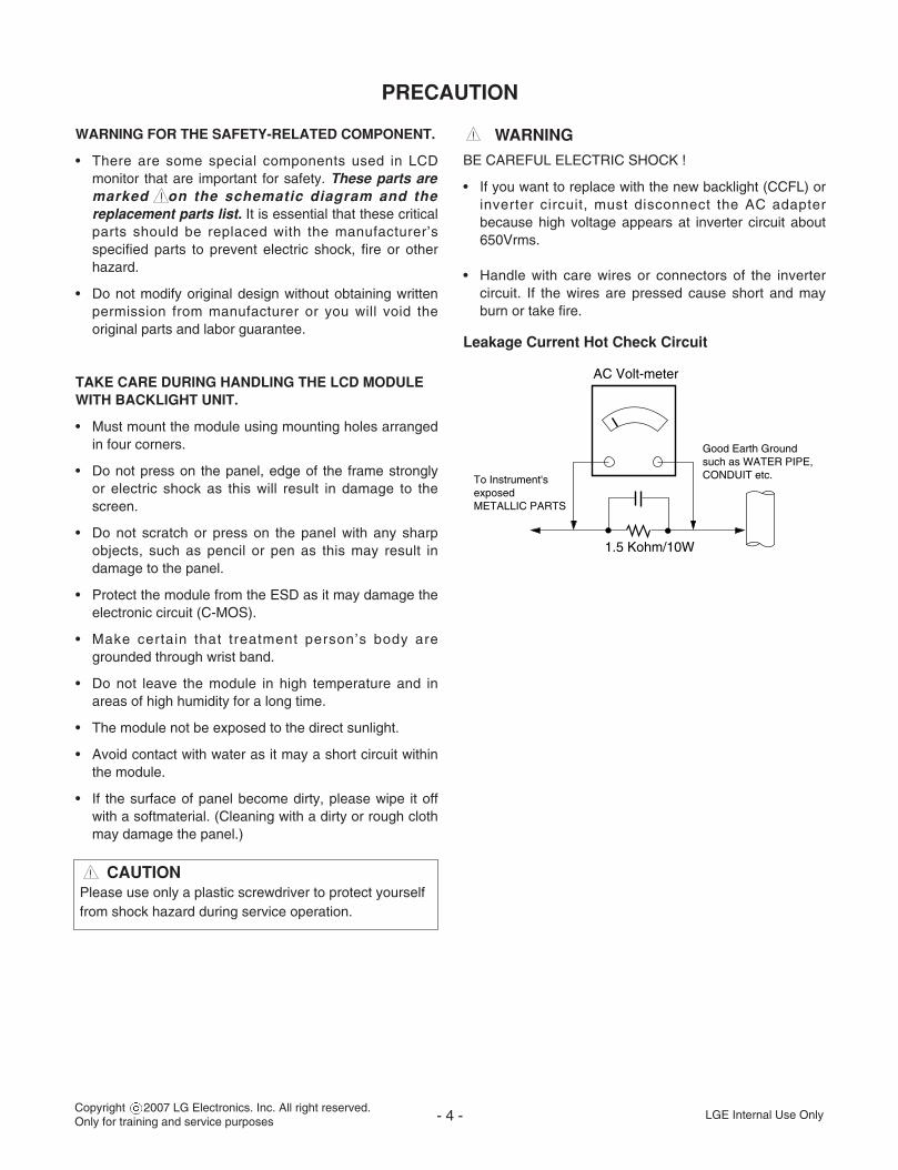
WARNING
BE CAREFUL ELECTRIC SHOCK !
• If you want to replace with the new backlight (CCFL) orinverter circuit, must disconnect the AC adapterbecause high voltage appears at inverter circuit about650Vrms.
• Handle with care wires or connectors of the invertercircuit. If the wires are pressed cause short and mayburn or take fire.
Leakage Current Hot Check Circuit
PRECAUTION
CAUTIONPlease use only a plastic screwdriver to protect yourselffrom shock hazard during service operation.
1.5 Kohm/10W
To Instrument'sexposed METALLIC PARTS
Good Earth Groundsuch as WATER PIPE,CONDUIT etc.
AC Volt-meter
- 5 -Copyright 2007 LG Electronics. Inc. All right reserved.Only for training and service purposes
LGE Internal Use Only
SERVICING PRECAUTIONSCAUTION: Before servicing receivers covered by thisservice manual and its supplements and addenda, readand follow the SAFETY PRECAUTIONS on page 3 of thispublication.NOTE: If unforeseen circumstances create conflictbetween the following servicing precautions and any of thesafety precautions on page 3 of this publication, alwaysfollow the safety precautions. Remember: Safety First.
General Servicing Precautions1. Always unplug the receiver AC power cord from the AC
power source before;a. Removing or reinstalling any component, circuit
board module or any other receiver assembly.b. Disconnecting or reconnecting any receiver electrical
plug or other electrical connection.c. Connecting a test substitute in parallel with an
electrolytic capacitor in the receiver.CAUTION: A wrong part substitution or incorrectpolarity installation of electrolytic capacitors mayresult in an explosion hazard.
d. Discharging the picture tube anode.2. Test high voltage only by measuring it with an
appropriate high voltage meter or other voltagemeasuring device (DVM, FETVOM, etc) equipped witha suitable high voltage probe.Do not test high voltage by "drawing an arc".
3. Discharge the picture tube anode only by (a) firstconnecting one end of an insulated clip lead to thedegaussing or kine aquadag grounding system shieldat the point where the picture tube socket ground leadis connected, and then (b) touch the other end of theinsulated clip lead to the picture tube anode button,using an insulating handle to avoid personal contactwith high voltage.
4. Do not spray chemicals on or near this receiver or anyof its assemblies.
5. Unless specified otherwise in this service manual,clean electrical contacts only by applying the followingmixture to the contacts with a pipe cleaner, cotton-tipped stick or comparable non-abrasive applicator;10% (by volume) Acetone and 90% (by volume)isopropyl alcohol (90%-99% strength)CAUTION: This is a flammable mixture.Unless specified otherwise in this service manual,lubrication of contacts in not required.
6. Do not defeat any plug/socket B+ voltage interlockswith which receivers covered by this service manualmight be equipped.
7. Do not apply AC power to this instrument and/or any ofits electrical assemblies unless all solid-state deviceheat sinks are correctly installed.
8. Always connect the test receiver ground lead to thereceiver chassis ground before connecting the testreceiver positive lead.Always remove the test receiver ground lead last.
9. Use with this receiver only the test fixtures specified inthis service manual.CAUTION: Do not connect the test fixture ground strapto any heat sink in this receiver.
Electrostatically Sensitive (ES) DevicesSome semiconductor (solid-state) devices can bedamaged easily by static electricity. Such componentscommonly are called Electrostatically Sensitive (ES)Devices. Examples of typical ES devices are integratedcircuits and some field-effect transistors andsemiconductor "chip" components. The followingtechniques should be used to help reduce the incidence ofcomponent damage caused by static by static electricity.1. Immediately before handling any semiconductor
component or semiconductor-equipped assembly, drainoff any electrostatic charge on your body by touching aknown earth ground. Alternatively, obtain and wear acommercially available discharging wrist strap device,which should be removed to prevent potential shockreasons prior to applying power to the unit under test.
2. After removing an electrical assembly equipped withES devices, place the assembly on a conductivesurface such as aluminum foil, to prevent electrostaticcharge buildup or exposure of the assembly.
3. Use only a grounded-tip soldering iron to solder orunsolder ES devices.
4. Use only an anti-static type solder removal device.Some solder removal devices not classified as "anti-static" can generate electrical charges sufficient todamage ES devices.
5. Do not use freon-propelled chemicals. These cangenerate electrical charges sufficient to damage ESdevices.
6. Do not remove a replacement ES device from itsprotective package until immediately before you areready to install it. (Most replacement ES devices arepackaged with leads electrically shorted together byconductive foam, aluminum foil or comparableconductive material).
7. Immediately before removing the protective materialfrom the leads of a replacement ES device, touch theprotective material to the chassis or circuit assemblyinto which the device will be installed.CAUTION: Be sure no power is applied to the chassisor circuit, and observe all other safety precautions.
8. Minimize bodily motions when handling unpackagedreplacement ES devices. (Otherwise harmless motionsuch as the brushing together of your clothes fabric orthe lifting of your foot from a carpeted floor cangenerate static electricity sufficient to damage an ESdevice.)
- 6 -Copyright 2007 LG Electronics. Inc. All right reserved.Only for training and service purposes
LGE Internal Use Only
General Soldering Guidelines1. Use a grounded-tip, low-wattage soldering iron and
appropriate tip size and shape that will maintain tiptemperature within the range or 500 F to 600 F.
2. Use an appropriate gauge of RMA resin-core soldercomposed of 60 parts tin/40 parts lead.
3. Keep the soldering iron tip clean and well tinned.4. Thoroughly clean the surfaces to be soldered. Use a
mall wire-bristle (0.5 inch, or 1.25cm) brush with ametal handle.Do not use freon-propelled spray-on cleaners.
5. Use the following unsoldering techniquea. Allow the soldering iron t ip to reach normal
temperature.(500 F to 600 F)
b. Heat the component lead until the solder melts.c. Quickly draw the melted solder with an anti-static,
suction-type solder removal device or with solderbraid.CAUTION: Work quickly to avoid overheating thecircuitboard printed foil.
6. Use the following soldering technique.a. Allow the soldering iron tip to reach a normal
temperature (500 F to 600 F)b. First, hold the soldering iron tip and solder the strand
against the component lead until the solder melts.
c. Quickly move the soldering iron tip to the junction ofthe component lead and the printed circuit foil, andhold it there only until the solder flows onto andaround both the component lead and the foil.CAUTION: Work quickly to avoid overheating thecircuit board printed foil.
d. Closely inspect the solder area and remove anyexcess or splashed solder with a small wire-bristlebrush.
IC Remove/ReplacementSome chassis circuit boards have slotted holes (oblong)through which the IC leads are inserted and then bent flatagainst the circuit foil. When holes are the slotted type,the following technique should be used to remove andreplace the IC. When working with boards using thefamiliar round hole, use the standard technique asoutlined in paragraphs 5 and 6 above.
Removal1. Desolder and straighten each IC lead in one operation
by gently prying up on the lead with the soldering irontip as the solder melts.
2. Draw away the melted solder with an anti-staticsuction-type solder removal device (or with solderbraid) before removing the IC.
Replacement1. Carefully insert the replacement IC in the circuit board.2. Carefully bend each IC lead against the circuit foil pad
and solder it.3. Clean the soldered areas with a small wire-bristle
brush. (It is not necessary to reapply acrylic coating tothe areas).
"Small-Signal" Discrete TransistorRemoval/Replacement1. Remove the defective transistor by clipping its leads as
close as possible to the component body.2. Bend into a "U" shape the end of each of three leads
remaining on the circuit board.3. Bend into a "U" shape the replacement transistor leads.4. Connect the replacement transistor leads to the
corresponding leads extending from the circuit boardand crimp the "U" with long nose pliers to insure metalto metal contact then solder each connection.
Power Output, Transistor DeviceRemoval/Replacement1. Heat and remove all solder from around the transistor
leads.2. Remove the heat sink mounting screw (if so equipped).3. Carefully remove the transistor from the heat sink of the
circuit board.4. Insert new transistor in the circuit board.5. Solder each transistor lead, and clip off excess lead.6. Replace heat sink.
Diode Removal/Replacement1. Remove defective diode by clipping its leads as close
as possible to diode body.2. Bend the two remaining leads perpendicular y to the
circuit board.3. Observing diode polarity, wrap each lead of the new
diode around the corresponding lead on the circuitboard.
4. Securely crimp each connection and solder it.5. Inspect (on the circuit board copper side) the solder
joints of the two "original" leads. If they are not shiny,reheat them and if necessary, apply additional solder.
Fuse and Conventional ResistorRemoval/Replacement1. Clip each fuse or resistor lead at top of the circuit board
hollow stake.2. Securely crimp the leads of replacement component
around notch at stake top.3. Solder the connections.
CAUTION: Maintain original spacing between thereplaced component and adjacent components and thecircuit board to prevent excessive componenttemperatures.
- 7 -Copyright 2007 LG Electronics. Inc. All right reserved.Only for training and service purposes
LGE Internal Use Only
Circuit Board Foil RepairExcessive heat applied to the copper foil of any printedcircuit board will weaken the adhesive that bonds the foilto the circuit board causing the foil to separate from or"l i f t-off" the board. The following guidelines andprocedures should be followed whenever this condition isencountered.
At IC ConnectionsTo repair a defective copper pattern at IC connections usethe following procedure to install a jumper wire on thecopper pattern side of the circuit board. (Use thistechnique only on IC connections).
1. Carefully remove the damaged copper pattern with asharp knife. (Remove only as much copper asabsolutely necessary).
2. carefully scratch away the solder resist and acryliccoating (if used) from the end of the remaining copperpattern.
3. Bend a small "U" in one end of a small gauge jumperwire and carefully crimp it around the IC pin. Solder theIC connection.
4. Route the jumper wire along the path of the out-awaycopper pattern and let it overlap the previously scrapedend of the good copper pattern. Solder the overlappedarea and clip off any excess jumper wire.
At Other ConnectionsUse the following technique to repair the defective copperpattern at connections other than IC Pins. This techniqueinvolves the installation of a jumper wire on thecomponent side of the circuit board.1. Remove the defective copper pattern with a sharp
knife.Remove at least 1/4 inch of copper, to ensure that ahazardous condition will not exist if the jumper wireopens.
2. Trace along the copper pattern from both sides of thepattern break and locate the nearest component that isdirectly connected to the affected copper pattern.
3. Connect insulated 20-gauge jumper wire from the leadof the nearest component on one side of the patternbreak to the lead of the nearest component on theother side.Carefully crimp and solder the connections.CAUTION: Be sure the insulated jumper wire isdressed so the it does not touch components or sharpedges.
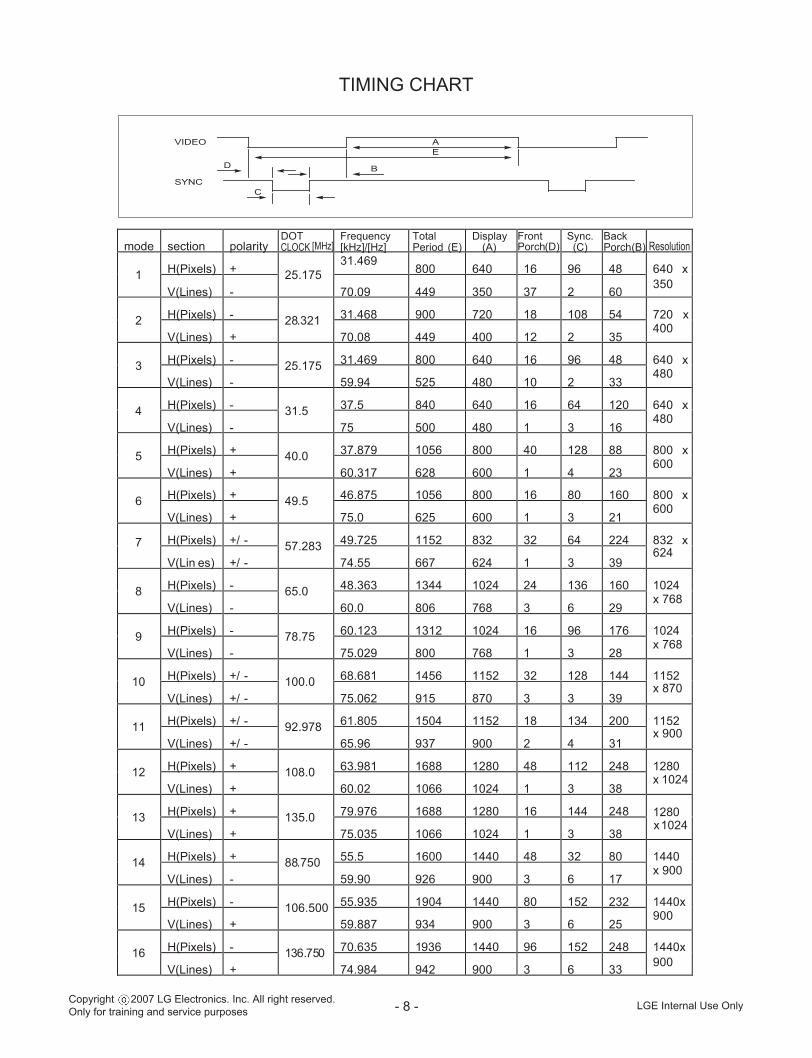
TIMING CHART
- 8 -Copyright 2007 LG Electronics. Inc. All right reserved.Only for training and service purposes LGE Internal Use Only
mode section polarity DOT
CLOCK
[MHz]
Frequency [kHz]/[Hz]
Total Period (E)
Display (A)
FrontPorch
(D)
Sync. (C)
Back Porch
(B) Resolution
H(Pixels) + 31.469
800 640 16 96 48 1V(Lines) -
25.175 70.09 449 350 37 2 60
640 x 350
H(Pixels) - 31.468 900 720 18 108 54 2 V(Lines) +
28.321 70.08 449 400 12 2 35
720 x 400
H(Pixels) - 31.469 800 640 16 96 48 3 V(Lines) -
25.175 59.94 525 480 10 2 33
640 x 480
H(Pixels) - 37.5 840 640 16 64 120 4 V(Lines) -
31.5 75 500 480 1 3 16
640 x 480
H(Pixels) + 37.879 1056 800 40 128 88 5 V(Lines) +
40.0 60.317 628 600 1 4 23
800 x 600
H(Pixels) + 46.875 1056 800 16 80 160 6 V(Lines) +
49.5 75.0 625 600 1 3 21
800 x 600
H(Pixels) +/ - 49.725 1152 832 32 64 224 7
V(Lin es) +/ - 57.283
74.55 667 624 1 3 39
832 x 624
H(Pixels) - 48.363 1344 1024 24 136 160 8 V(Lines) -
65.0 60.0 806 768 3 6 29
1024 x 768
H(Pixels) - 60.123 1312 1024 16 96 176 9V(Lines) -
78.75 75.029 800 768 1 3 28
1024 x 768
H(Pixels) +/ - 68.681 1456 1152 32 128 144 10V(Lines) +/ -
100.0 75.062 915 870 3 3 39
1152 x 870
H(Pixels) +/ - 61.805 1504 1152 18 134 200 11 V(Lines) +/ -
92.978 65.96 937 900 2 4 31
1152 x 900
H(Pixels) + 63.981 1688 1280 48 112 248 12 V(Lines) +
108.0 60.02 1066 1024 1 3 38
1280 x
1024H(Pixels) + 79.976 1688 1280 16 144 248 13 V(Lines) +
135.0 75.035 1066 1024 1 3 38
1280 x
1024
H(Pixels) + 55.5 1600 1440 48 32 80 14 V(Lines) -
88.750 59.90 926 900 3 6 17
1440 x 900
H(Pixels) - 55.935 1904 1440 80 152 232 15 V(Lines) +
106.500 59.887 934 900 3 6 25
1440x 900
H(Pixels) - 70.635 1936 1440 96 152 248 16 V(Lines) +
136.750 74.984 942 900 3 6 33
1440x 900
VIDEO
SYNC
AE
D B
C
-9 -
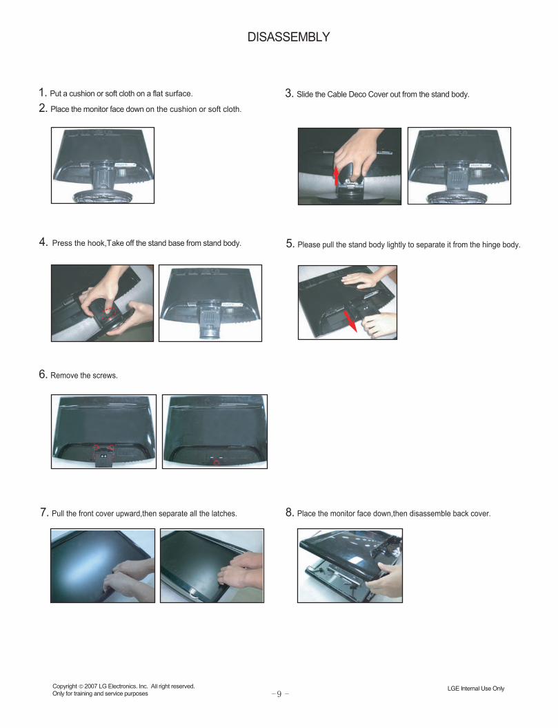
DISASSEMBLY
1. Put a cushion or soft cloth on a flat surface.
4. Press the hook,Take off the stand base from stand body. 5. Please pull the stand body lightly to separate it from the hinge body.
6. Remove the screws.
7. Pull the front cover upward,then separate all the latches. 8. Place the monitor face down,then disassemble back cover.
2. Place the monitor face down on the cushion or soft cloth.
3. Slide the Cable Deco Cover out from the stand body.
- 10 -Copyright 2007 LG Electronics. Inc. All right reserved.Only for training and service purposes LGE Internal Use Only
S D
V L)B/G/R(I golanA
D-Sub
SPIL
retliF
V5 V5 1V 5
rot al ugeR
V3.3
c cV V5
V3.3
)s pma L2 (retrev nI
V51
DVI-D
)SDMT(IVD
KEY
V8.1
V8.1
Module
ADSLCS/
MORPEE)DIDE(
MORPEE)m etsy S(
V3.3
MORPEE)DIDE (
1440
x900
@60
Hz
z hM10
6.5
lau Deca fret nI
en ig nE
ya lpsiDcorP
gn issee nign E
es nopse Re miT
t nemecnah nE
SDVLlenaP
ec afretnI
DSOkco lC
rota reneGUCM
MAR D
TSU
MU
58B
MOR hsal F
V3.3
l ats yr C
zHM8 13.4 1
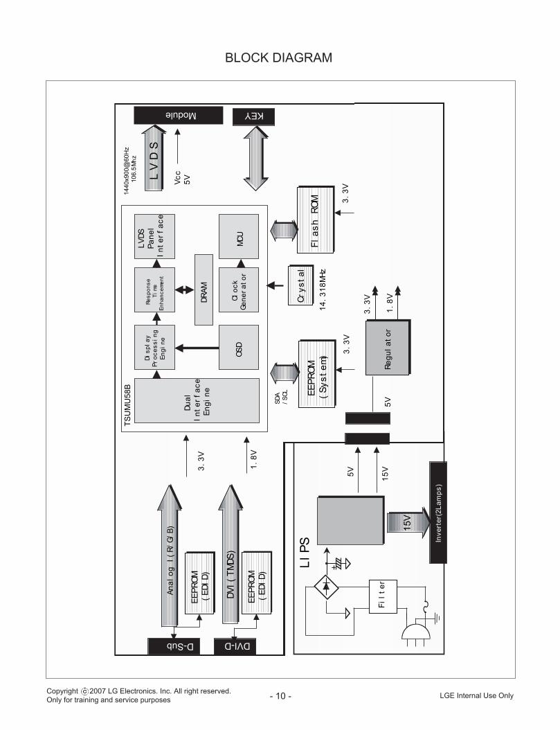
BLOCK DIAGRAM
- 11 -Copyright 2007 LG Electronics. Inc. All right reserved.Only for training and service purposes
LGE Internal Use Only
DESCRIPTION OF BLOCK DIAGRAM
1. Video Controller Part.This part amplifies the level of video signal for the digital conversion and converts from the analog video signal to thedigital video signal using a pixel clock.The pixel clock for each mode is generated by the PLL.The range of the pixel clock is 136MHz In W1752T.This part consists of the Scaler, ADC convertor, TMDS receiver and LVDS transmitter.The Scaler gets the video signal converted analog to digital, interpolates input to 1440X900(W1752T)resolution signal and outputs 8-bit R, G, B signal to transmitter.
2. Power Part.This part consists of the one 3.3V, and one 1.8V regulators to convert power which is provided 5V in Power board.15V is provided for inverter in W1752T.Also, 5V is converted 3.3V and 1.8V by regulator. Converted power is provided for IC in the main board.The inverter converts from DC 15V to AC 700Vrms and operates back-light lamps of module in W1752T.
3. MICOM Part.This part is include video controller part. And this part consists of EEPROM IC , control data, Reset IC and the Micom.The Micom distinguishes polarity and frequency of the H/V sync are supplied from signal cable.The controlled data of each modes is stored in EEPROM.
- 12 -
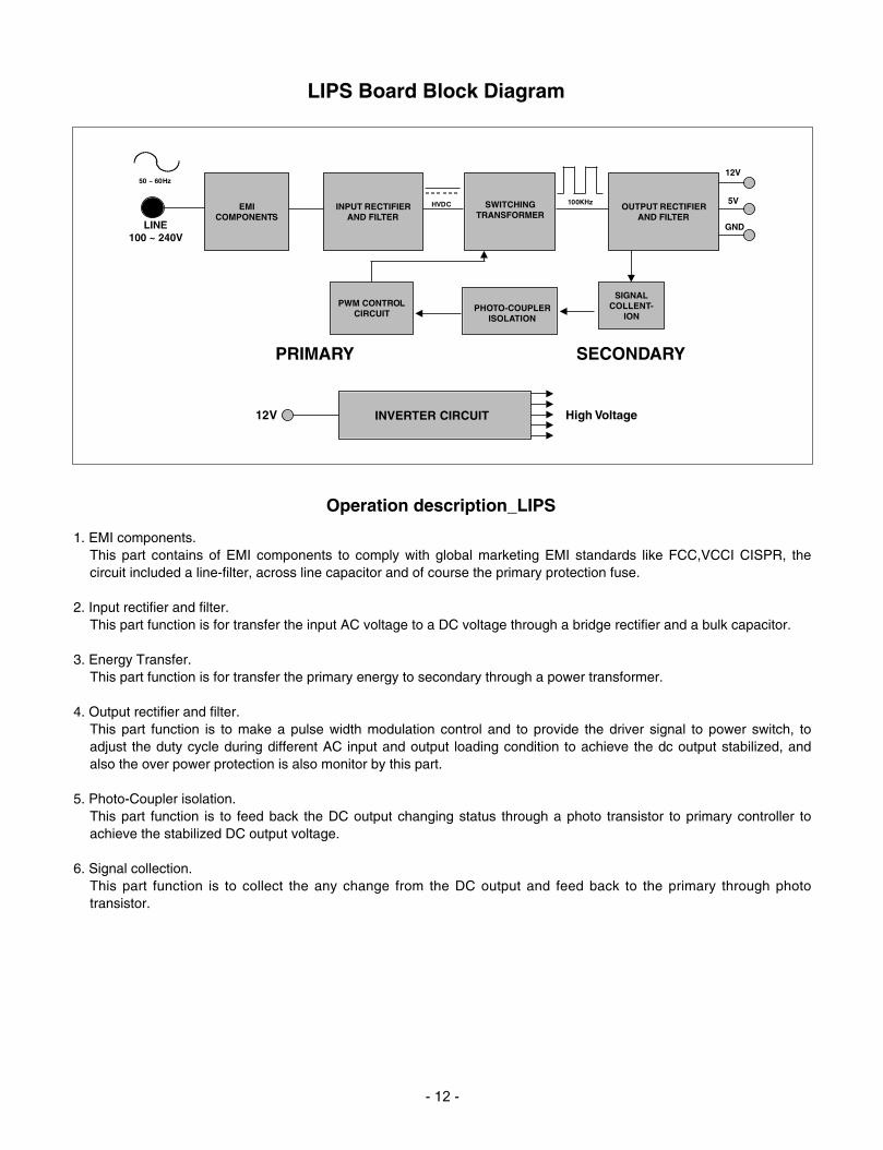
LIPS Board Block Diagram
EMICOMPONENTS
LINE100 ~ 240V
INPUT RECTIFIERAND FILTER
SWITCHINGTRANSFORMER
OUTPUT RECTIFIERAND FILTER
12V
5V
GND
SIGNALCOLLENT-
IONPHOTO-COUPLER
ISOLATION
PWM CONTROLCIRCUIT
HVDC 100KHz
PRIMARY SECONDARY
50 ~ 60Hz
INVERTER CIRCUIT High Voltage12V
Operation description_LIPS
1. EMI components.This part contains of EMI components to comply with global marketing EMI standards like FCC,VCCI CISPR, thecircuit included a line-filter, across line capacitor and of course the primary protection fuse.
2. Input rectifier and filter.This part function is for transfer the input AC voltage to a DC voltage through a bridge rectifier and a bulk capacitor.
3. Energy Transfer.This part function is for transfer the primary energy to secondary through a power transformer.
4. Output rectifier and filter.This part function is to make a pulse width modulation control and to provide the driver signal to power switch, toadjust the duty cycle during different AC input and output loading condition to achieve the dc output stabilized, andalso the over power protection is also monitor by this part.
5. Photo-Coupler isolation.This part function is to feed back the DC output changing status through a photo transistor to primary controller toachieve the stabilized DC output voltage.
6. Signal collection.This part function is to collect the any change from the DC output and feed back to the primary through phototransistor.
- 13 -Copyright 2007 LG Electronics. Inc. All right reserved.Only for training and service purposes
LGE Internal Use Only
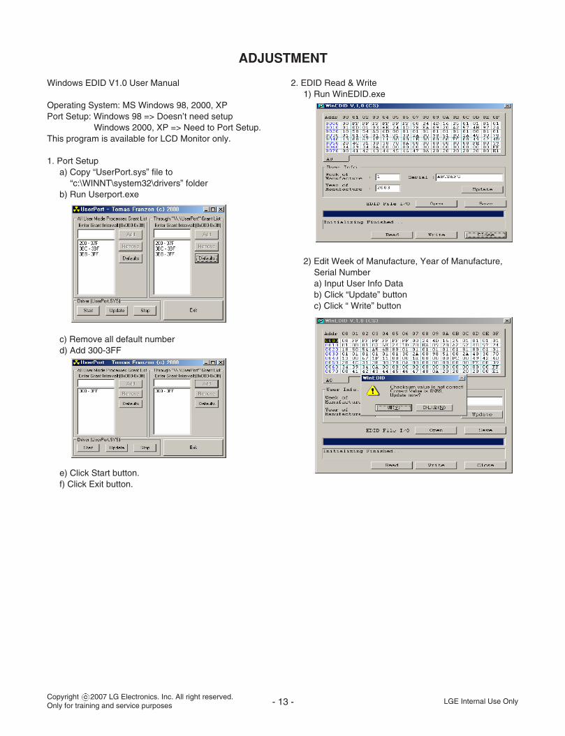
ADJUSTMENT
Windows EDID V1.0 User Manual
Operating System: MS Windows 98, 2000, XPPort Setup: Windows 98 => Doesn’t need setup
Windows 2000, XP => Need to Port Setup.This program is available for LCD Monitor only.
1. Port Setupa) Copy “UserPort.sys” file to
“c:\WINNT\system32\drivers” folderb) Run Userport.exe
c) Remove all default numberd) Add 300-3FF
e) Click Start button.f) Click Exit button.
2. EDID Read & Write1) Run WinEDID.exe
2) Edit Week of Manufacture, Year of Manufacture, Serial Numbera) Input User Info Datab) Click “Update” buttonc) Click “ Write” button
- 14 -Copyright 2007 LG Electronics. Inc. All right reserved.Only for training and service purposes LGE Internal Use Only
220
IBMCompatible PC
PARALLEL PORT
Power inlet (required)
Power LED
ST Switch
Power Select Switch(110V/220V)
eniL lortnoC
desu toN
C232SR
LELLARAP
CNYS-V
OPW
RE
TS
SGV
ROTINOM
E
E
V-Sync On/Off Switch(Switch must be ON.)
F
F
A
A
BB
C
C
15105
569
1
1
114
1325
6
5V
5V
5V
4.7K4.7K
4.7K
74LS06
74LS06
OFF ON
OFF
ON
11Video SignalGenerator
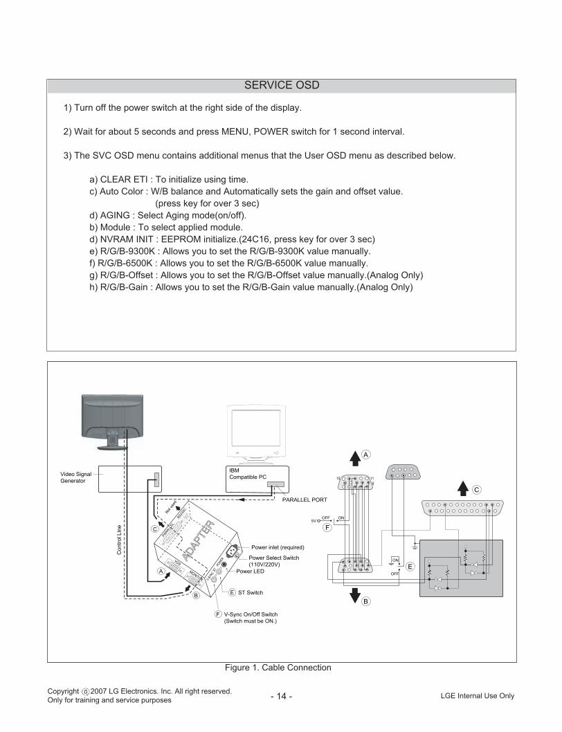
Figure 1. Cable Connection
SERVICE OSD
1) Turn off the power switch at the right side of the display.
2) Wait for about 5 seconds and press MENU, POWER switch for 1 second interval.
3) The SVC OSD menu contains additional menus that the User OSD menu as described below.
a) CLEAR ETI : To initialize using time.c) Auto Color : W/B balance and Automatically sets the gain and offset value.
(press key for over 3 sec)d) AGING : Select Aging mode(on/off).b) Module : To select applied module.d) NVRAM INIT : EEPROM initialize.(24C16, press key for over 3 sec)e) R/G/B-9300K : Allows you to set the R/G/B-9300K value manually.f) R/G/B-6500K : Allows you to set the R/G/B-6500K value manually.g) R/G/B-Offset : Allows you to set the R/G/B-Offset value manually.(Analog Only)h) R/G/B-Gain : Allows you to set the R/G/B-Gain value manually.(Analog Only)
- 15 -Copyright 2007 LG Electronics. Inc. All right reserved.Only for training and service purposes
LGE Internal Use Only
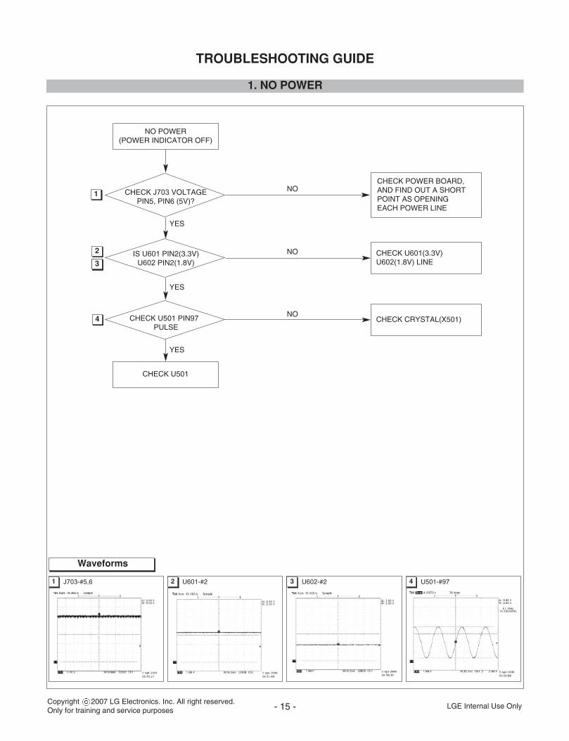
TROUBLESHOOTING GUIDE
1. NO POWER
NO POWER(POWER INDICATOR OFF)
CHECK U501
NO
NO
CHECK POWER BOARD,AND FIND OUT A SHORTPOINT AS OPENING EACH POWER LINE
CHECK U601(3.3V)U602(1.8V) LINE
NOCHECK CRYSTAL(X501)
YES
YES
YES
CHECK J703 VOLTAGE PIN5, PIN6 (5V)?
IS U601 PIN2(3.3V)U602 PIN2(1.8V)
CHECK U501 PIN97 PULSE
1
2
13
14
Waveforms
1 J703-#5,6 2 U601-#2 3 U602-#2 4 U501-#97
- 16 -Copyright 2007 LG Electronics. Inc. All right reserved.Only for training and service purposes
LGE Internal Use Only
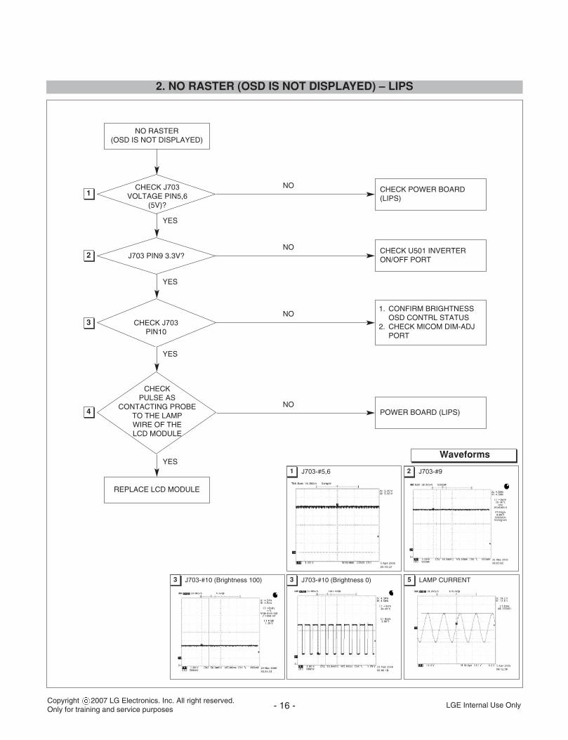
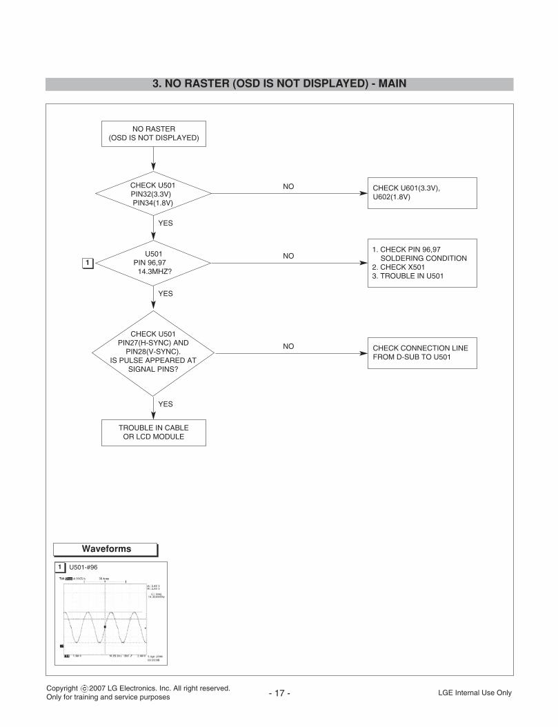
2. NO RASTER (OSD IS NOT DISPLAYED) – LIPS
CHECK U501 INVERTERON/OFF PORTJ703 PIN9 3.3V?
NO RASTER(OSD IS NOT DISPLAYED)
CHECK POWER BOARD(LIPS)
CHECK J703VOLTAGE PIN5,6
(5V)?
NO
NO
NO
NO
1. CONFIRM BRIGHTNESSOSD CONTRL STATUS
2. CHECK MICOM DIM-ADJ PORT
CHECK J703 PIN10
POWER BOARD (LIPS)
CHECK PULSE AS
CONTACTING PROBE TO THE LAMP WIRE OF THE LCD MODULE
REPLACE LCD MODULE
YES
1
2
3
4
YES
YES
YESWaveforms
1 J703-#5,6 2 J703-#9
3 J703-#10 (Brightness 100) 5 LAMP CURRENT3 J703-#10 (Brightness 0)
- 17 -Copyright 2007 LG Electronics. Inc. All right reserved.Only for training and service purposes
LGE Internal Use Only
3. NO RASTER (OSD IS NOT DISPLAYED) - MAIN
1. CHECK PIN 96,97SOLDERING CONDITION
2. CHECK X5013. TROUBLE IN U501
CHECK U501PIN32(3.3V)PIN34(1.8V)
NO
NO
NO
CHECK U601(3.3V),U602(1.8V)
U501PIN 96,97
14.3MHZ?
CHECK CONNECTION LINE FROM D-SUB TO U501
TROUBLE IN CABLE OR LCD MODULE
YES
YES
NO RASTER(OSD IS NOT DISPLAYED)
CHECK U501 PIN27(H-SYNC) AND
PIN28(V-SYNC). IS PULSE APPEARED AT
SIGNAL PINS?
YES
1
Waveforms
1 U501-#96
- 18 -Copyright 2007 LG Electronics. Inc. All right reserved.Only for training and service purposes
LGE Internal Use Only
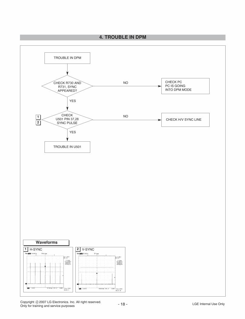
4. TROUBLE IN DPM
TROUBLE IN DPM
TROUBLE IN U501
CHECK PC PC IS GOINGINTO DPM MODE
NO
CHECK H/V SYNC LINENO
YES
CHECK R730 ANDR731, SYNCAPPEARED?
CHECKU501 PIN 37,28SYNC PULSE
YES
1 H-SYNC 2 V-SYNC
Waveforms
1
2
300
Copyright 2007 LG Electronics. Inc. All right reserved.Only for training and service purposes LGE Internal Use Only
400
900
910
920 93
0
200
410
420
500
510
430
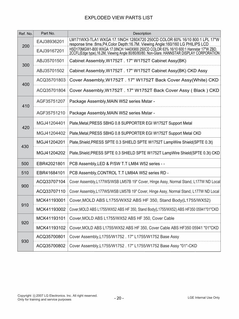
EXPLODED VIEW PARTS LIST
- 20 -
DescriptionPart No.Ref. No.
300
430MGJ41204201 Plate,Shield,PRESS SPTE 0.3 SHIELD SPTE W1752T LampWire Shield(SPTE 0.3t)
MGJ41204202 Plate,Shield,PRESS SPTE 0.3 SHIELD SPTE W1752T LampWire Shield(SPTE 0.3t) CKD
EBR42021801 PCB Assembly,LED & P/SW T.T LM84 W52 series - -
EBR41684101 PCB Assembly,CONTROL T.T LM84A W52 series RD -
Cabinet Assembly,W1752T . 17" W1752T Cabinet Assy(BK)
500
510
900
910
920
ACQ33707104 Cover Assembly,L177WS/WSB LM57B 19" Cover, Hinge Assy, Normal Stand, L177W ND Local
ACQ33707110 Cover Assembly,L177WS/WSB LM57B 19" Cover, Hinge Assy, Normal Stand, L177W ND Local
MCK41193001 Cover,MOLD ABS L1755/WX52 ABS HF 350, Stand Body(L1755/WX52)
MCK41193002 Cover,MOLD ABS L1755/WX52 ABS HF 350, Stand Body(L1755/WX52) ABS HF350 05941"01"CKD
MCK41193101 Cover,MOLD ABS L1755/WX52 ABS HF 350, Cover Cable
MCK41193102 Cover,MOLD ABS L1755/WX52 ABS HF 350, Cover Cable ABS HF350 05941 "01"CKD
930ACQ35700801 Cover Assembly,L1755/W1752 . 17" L1755/W1752 Base Assy
ACQ35700802 Cover Assembly,L1755/W1752 . 17" L1755/W1752 Base Assy "01"-CKD
ABJ35701501
Cabinet Assembly,W1752T . 17" W1752T Cabinet Assy(BK) CKD AssyABJ35701502
LM171WX3-TLA1 WXGA 17.1INCH 1280X720 250CD COLOR 60% 16/10 800:1 LPL 17"W response time :8ms,P4,Color Depth:16.7M. Viewing Angle:160/160 LG PHILIPS LCD EAJ38936201
HSD170MGW1-B00 WXGA 17.0INCH 1440X900 250CD COLOR 63% 16/10 600:1 Hannstar 17"W ZBD, 2CCFL(Edge type),16.2M, Viewing Angle 80/80/80/80. Non-Glare. HANNSTAR DISPLAY CORPORATION EAJ39167201
200
410Package Assembly,MAIN W52 series Mstar - AGF35751207
Package Assembly,MAIN W52 series Mstar - AGF35751210
420Plate,Metal,PRESS SBHG 0.8 SUPPORTER EGI W1752T Support Metal MGJ41204401
Plate,Metal,PRESS SBHG 0.8 SUPPORTER EGI W1752T Support Metal CKD
MGJ41204402
400Cover Assembly,W1752T . 17" W1752T Back Cover Assy(White) CKDACQ35701803
Cover Assembly,W1752T . 17" W1752T Back Cover Assy ( Black ) CKD ACQ35701804
Copyright 2007 LG Electronics. Inc. All right reserved.Only for training and service purposes LGE Internal Use Only
LOC NO. PART NO. DESCRIPTION/SPECIFICATON
C501 0CK104CK56A “Capacitor,Ceramic,Chip,0603B104K500CT 100nF”C502 0CK473CK56A “Capacitor,Ceramic,Chip,C1608X7R1H473KT 47nF”C503 0CK473CK56A “Capacitor,Ceramic,Chip,C1608X7R1H473KT 47nF”C504 0CK473CK56A “Capacitor,Ceramic,Chip,C1608X7R1H473KT 47nF”C505 0CK473CK56A “Capacitor,Ceramic,Chip,C1608X7R1H473KT 47nF”C506 0CC102CK41A “Capacitor,Ceramic,Chip,C1608C0G1H102JT 1nF”C507 0CK473CK56A “Capacitor,Ceramic,Chip,C1608X7R1H473KT 47nF”C508 0CK473CK56A “Capacitor,Ceramic,Chip,C1608X7R1H473KT 47nF”C509 0CC270CK41A “Capacitor,Ceramic,Chip,C1608C0G1H270JT 27pF”C510 0CC270CK41A “Capacitor,Ceramic,Chip,C1608C0G1H270JT 27pF”C511 0CK104CK56A “Capacitor,Ceramic,Chip,0603B104K500CT 100nF”C512 0CE106CF638 “Capacitor,AL,Radial,SHL5.0TP16VB10M 10uF”C513 0CK104CK56A “Capacitor,Ceramic,Chip,0603B104K500CT 100nF”C514 0CK104CK56A “Capacitor,Ceramic,Chip,0603B104K500CT 100nF”C515 0CK104CK56A “Capacitor,Ceramic,Chip,0603B104K500CT 100nF”C516 0CK104CK56A “Capacitor,Ceramic,Chip,0603B104K500CT 100nF”C517 0CK104CK56A “Capacitor,Ceramic,Chip,0603B104K500CT 100nF”C518 0CK104CK56A “Capacitor,Ceramic,Chip,0603B104K500CT 100nF”C519 0CK104CK56A “Capacitor,Ceramic,Chip,0603B104K500CT 100nF”C520 0CK104CK56A “Capacitor,Ceramic,Chip,0603B104K500CT 100nF”C521 0CK104CK56A “Capacitor,Ceramic,Chip,0603B104K500CT 100nF”C522 0CK104CK56A “Capacitor,Ceramic,Chip,0603B104K500CT 100nF”C523 0CK104CK56A “Capacitor,Ceramic,Chip,0603B104K500CT 100nF”C524 0CK104CK56A “Capacitor,Ceramic,Chip,0603B104K500CT 100nF”C525 0CK104CK56A “Capacitor,Ceramic,Chip,0603B104K500CT 100nF”C526 0CK104CK56A “Capacitor,Ceramic,Chip,0603B104K500CT 100nF”C527 0CK104CK56A “Capacitor,Ceramic,Chip,0603B104K500CT 100nF”C601 0CE107EF610 “Capacitor,AL,Radial,KMG16VB100M 100uF 20”C602 0CK103CK51A “Capacitor,Ceramic,Chip,0603B103K500CT 10nF”C603 0CK475CC94A “Capacitor,Ceramic,Chip,C1608Y5V0J475ZT 4.7u”C604 0CE107EF610 “Capacitor,AL,Radial,KMG16VB100M 100uF 20”C605 0CE227EF638 “Capacitor,AL,Radial,KMG5.0TP16VB220M 220”C702 0CK103CK51A “Capacitor,Ceramic,Chip,0603B103K500CT 10nF”C703 0CK103CK51A “Capacitor,Ceramic,Chip,0603B103K500CT 10nF”C704 0CK104CK56A “Capacitor,Ceramic,Chip,0603B104K500CT 100nF”C705 0CK105CD56A “Capacitor,Ceramic,Chip,C1608X7R1A105KT 1uF”C706 0CC101CK41A “Capacitor,Ceramic,Chip,C1608C0G1H101JT 100p”C707 0CC101CK41A “Capacitor,Ceramic,Chip,C1608C0G1H101JT 100p”C708 0CC101CK41A “Capacitor,Ceramic,Chip,C1608C0G1H101JT 100p”C709 0CK104CK56A “Capacitor,Ceramic,Chip,0603B104K500CT 100nF”C710 0CK104CK56A “Capacitor,Ceramic,Chip,0603B104K500CT 100nF”C711 0CK104CK56A “Capacitor,Ceramic,Chip,0603B104K500CT 100nF”C712 0CK104CK56A “Capacitor,Ceramic,Chip,0603B104K500CT 100nF”C713 0CK104CK56A “Capacitor,Ceramic,Chip,0603B104K500CT 100nF”C714 0CK104CK56A “Capacitor,Ceramic,Chip,0603B104K500CT 100nF”C715 0CK104CK56A “Capacitor,Ceramic,Chip,0603B104K500CT 100nF”C716 0CK104CK56A “Capacitor,Ceramic,Chip,0603B104K500CT 100nF”C718 0CK104CK56A “Capacitor,Ceramic,Chip,0603B104K500CT 100nF”C719 0CK104CK56A “Capacitor,Ceramic,Chip,0603B104K500CT 100nF”C720 0CC680CK41A “Capacitor,Ceramic,Chip,C1608C0G1H680JT 68pF”C721 0CC680CK41A “Capacitor,Ceramic,Chip,C1608C0G1H680JT 68pF”C722 0CC680CK41A “Capacitor,Ceramic,Chip,C1608C0G1H680JT 68pF”C723 0CC680CK41A “Capacitor,Ceramic,Chip,C1608C0G1H680JT 68pF”
D702 0DSIH00018A “Diode,Switching,ENKMC2837-T112 1.2V”D703 0DSIH00018A “Diode,Switching,ENKMC2837-T112 1.2V”D704 0DSIH00018A “Diode,Switching,ENKMC2837-T112 1.2V”D705 0DSIH00018A “Diode,Switching,ENKMC2837-T112 1.2V”D706 0DSIH00018A “Diode,Switching,ENKMC2837-T112 1.2V”D707 0DSIH00018A “Diode,Switching,ENKMC2837-T112 1.2V”D708 0DSIH00018A “Diode,Switching,ENKMC2837-T112 1.2V”D709 0DSIH00018A “Diode,Switching,ENKMC2837-T112 1.2V”D710 0DD184009AA “Diode Assembly,KDS184 KDS184 TP KEC”D711 0DSIH00018A “Diode,Switching,ENKMC2837-T112 1.2V”
D712 0DSIH00018A “Diode,Switching,ENKMC2837-T112 1.2V”D713 0DSIH00018A “Diode,Switching,ENKMC2837-T112 1.2V”D715 0DSON00138A “Diode,Schottky,MMBD301LT1G 600MV 30”ZD10 0DZ560009GB “Diode,Zener,BZT52C5V6S-(F) 5.6V”ZD701 0DZ560009GB “Diode,Zener,BZT52C5V6S-(F) 5.6V”ZD702 0DZ560009GB “Diode,Zener,BZT52C5V6S-(F) 5.6V”ZD704 0DZ560009GB “Diode,Zener,BZT52C5V6S-(F) 5.6V”ZD705 0DZ560009GB “Diode,Zener,BZT52C5V6S-(F) 5.6V”ZD706 0DZ560009GB “Diode,Zener,BZT52C5V6S-(F) 5.6V”ZD707 0DZ560009GB “Diode,Zener,BZT52C5V6S-(F) 5.6V”ZD709 0DZ560009GB “Diode,Zener,BZT52C5V6S-(F) 5.6V”ZD710 0DZ560009GB “Diode,Zener,BZT52C5V6S-(F) 5.6V”ZD9 0DZ560009GB “Diode,Zener,BZT52C5V6S-(F) 5.6V”
U501 EAN39545901 “IC,Protocol Controller,TSUMU58BWHL-LF -0.3T”U502 EAN37157001 “IC,Serial Flash Memory,W25X20VSNIG 2MBIT 25”U503 0IMMR00203A “IC,EEPROM,FM24C08 8KBIT 1KX8BI”U601 0IPMGA0010A “IC,LDO Voltage Regulator,AZ1117H-3.3 4.75TO10”U602 0IPMG00049A “IC,LDO Voltage Regulator,AZ1117H-1.8TR/E1[H13”U603 0IMMR00014A “IC,EEPROM,M24C02-RMN6TP 2KBIT”
Q501 0TRKE80046A “TR,Bipolar,2N3904S NPN 6V 60V 4”Q601 0TRKE80046A “TR,Bipolar,2N3904S NPN 6V 60V 4”Q602 EBK39150701 “TR,Bipolar,KTA1241 PNP -8V -35V”Q701 0TR390609DC “TR,Bipolar,2N3906S-RTK PNP -5V”Q702 0TR390609DC “TR,Bipolar,2N3906S-RTK PNP -5V”
R1 0RJ1602D677 “Resistor,Chip,MCR03EZPJ163 16KOHM”R2 0RJ1602D677 “Resistor,Chip,MCR03EZPJ163 16KOHM”R3 0RJ1801D677 “Resistor,Chip,MCR03EZPJ182 1.8KOHM”R4 0RJ1801D677 “Resistor,Chip,MCR03EZPJ182 1.8KOHM”R5 0RJ2201D677 “Resistor,Chip,MCR03EZPJ222 2.2KOHM”R501 0RJ0562D677 “Resistor,Chip,MCR03EZPJ560 56OHM 5”R502 0RJ0562D677 “Resistor,Chip,MCR03EZPJ560 56OHM 5”R503 0RJ0562D677 “Resistor,Chip,MCR03EZPJ560 56OHM 5”R504 0RJ0562D677 “Resistor,Chip,MCR03EZPJ560 56OHM 5”R505 0RJ1001D677 “Resistor,Chip,MCR03EZPJ102 1KOHM 5”R506 0RJ0562D677 “Resistor,Chip,MCR03EZPJ560 56OHM 5”R507 0RJ0562D677 “Resistor,Chip,MCR03EZPJ560 56OHM 5”R508 0RJ1002D677 “Resistor,Chip,MCR03EZPJ103 10KOHM”R509 0RJ3900D677 “Resistor,Chip,MCR03EZPJ391 390OHM”R510 0RJ4700D677 “Resistor,Chip,MCR03EZPJ471 470OHM”R511 0RJ2002D677 “Resistor,Chip,MCR03EZPJ203. 20KOHM”R512 0RJ1002D677 “Resistor,Chip,MCR03EZPJ103 10KOHM”R513 0RJ1002D677 “Resistor,Chip,MCR03EZPJ103 10KOHM”R514 0RJ1002D677 “Resistor,Chip,MCR03EZPJ103 10KOHM”R515 0RJ1002D677 “Resistor,Chip,MCR03EZPJ103 10KOHM”R516 0RJ4701D677 “Resistor,Chip,MCR03EZPJ472 4.7KOHM”R517 0RJ4701D677 “Resistor,Chip,MCR03EZPJ472 4.7KOHM”R518 0RJ1000D677 “Resistor,Chip,MCR03EZPJ101 100OHM”R519 0RJ4701D677 “Resistor,Chip,MCR03EZPJ472 4.7KOHM”R520 0RJ0332D677 “Resistor,Chip,MCR03EZPJ330 33OHM 5”R521 0RJ0332D677 “Resistor,Chip,MCR03EZPJ330 33OHM 5”R522 0RJ4701D677 “Resistor,Chip,MCR03EZPJ472 4.7KOHM”R524 0RJ0000D677 “Resistor,Chip,MCR03EZPJ000 0OHM 5%”R525 0RJ0000D677 “Resistor,Chip,MCR03EZPJ000 0OHM 5%”R527 0RJ4700D677 “Resistor,Chip,MCR03EZPJ471 470OHM”R528 0RJ4701D677 “Resistor,Chip,MCR03EZPJ472 4.7KOHM”R6 0RJ2201D677 “Resistor,Chip,MCR03EZPJ222 2.2KOHM”R601 0RJ3601D677 “Resistor,Chip,MCR03EZPJ362 3.6KOHM”R602 0RJ3900D677 “Resistor,Chip,MCR03EZPJ391 390OHM”R603 0RJ3900D677 “Resistor,Chip,MCR03EZPJ391 390OHM”R604 0RJ1002D677 “Resistor,Chip,MCR03EZPJ103 10KOHM”
REPLACEMENT PARTS LIST
DATE:2007.12.10LOC NO. PART NO. DESCRIPTION/SPECIFICATON
- 21 -
CAPACITORs
DIODEs
ICs
TRANSISTORs
RESISTORs
Copyright 2007 LG Electronics. Inc. All right reserved.Only for training and service purposes LGE Internal Use Only
R605 0RX0681K668 “Resistor,Metal Oxide Film,RSD02F36R80J 6.8OHM”R606 0RJ0000D677 “Resistor,Chip,MCR03EZPJ000 0OHM 5%”R607 0RH1002D622 “Resistor,Chip,MCR10EZHJ103 10KOHM”R608 0RJ1002D677 “Resistor,Chip,MCR03EZPJ103 10KOHM”R701 0RJ0000D677 “Resistor,Chip,MCR03EZPJ000 0OHM 5%”R702 0RJ4701D677 “Resistor,Chip,MCR03EZPJ472 4.7KOHM”R703 0RJ4701D677 “Resistor,Chip,MCR03EZPJ472 4.7KOHM”R704 0RJ0472D677 “Resistor,Chip,MCR03EZPJ470 47OHM 5”R705 0RJ0752D677 “Resistor,Chip,MCR03EZPJ750 75OHM 5”R706 0RJ1000D677 “Resistor,Chip,MCR03EZPJ101 100OHM”R707 0RJ1000D677 “Resistor,Chip,MCR03EZPJ101 100OHM”R708 0RJ1000D677 “Resistor,Chip,MCR03EZPJ101 100OHM”R709 0RJ2001D677 “Resistor,Chip,MCR03EZPJ202 2KOHM 5”R710 0RJ4701D677 “Resistor,Chip,MCR03EZPJ472 4.7KOHM”R711 0RJ4701D677 “Resistor,Chip,MCR03EZPJ472 4.7KOHM”R712 0RJ0000D677 “Resistor,Chip,MCR03EZPJ000 0OHM 5%”R713 0RJ0122D677 “Resistor,Chip,MCR03EZPJ120 12OHM 5”R714 0RJ0122D677 “Resistor,Chip,MCR03EZPJ120 12OHM 5”R715 0RJ0122D677 “Resistor,Chip,MCR03EZPJ120 12OHM 5”R716 0RJ0122D677 “Resistor,Chip,MCR03EZPJ120 12OHM 5”R717 0RJ0122D677 “Resistor,Chip,MCR03EZPJ120 12OHM 5”R718 0RJ0122D677 “Resistor,Chip,MCR03EZPJ120 12OHM 5”R719 0RJ0222D677 “Resistor,Chip,MCR03EZPJ220 22OHM 5”R720 0RJ0222D677 “Resistor,Chip,MCR03EZPJ220 22OHM 5”R721 0RJ4700D677 “Resistor,Chip,MCR03EZPJ471 470OHM”R722 0RJ4701D677 “Resistor,Chip,MCR03EZPJ472 4.7KOHM”R723 0RJ4701D677 “Resistor,Chip,MCR03EZPJ472 4.7KOHM”R724 0RJ0332D677 “Resistor,Chip,MCR03EZPJ330 33OHM 5”R725 0RJ0332D677 “Resistor,Chip,MCR03EZPJ330 33OHM 5”R726 0RJ4701D677 “Resistor,Chip,MCR03EZPJ472 4.7KOHM”R727 0RJ4701D677 “Resistor,Chip,MCR03EZPJ472 4.7KOHM”R728 0RJ0332D677 “Resistor,Chip,MCR03EZPJ330 33OHM 5”R729 0RJ0000D677 “Resistor,Chip,MCR03EZPJ000 0OHM 5%”R730 0RJ0682D677 “Resistor,Chip,MCR03EZPJ680 68OHM 5”R731 0RJ0682D677 “Resistor,Chip,MCR03EZPJ680 68OHM 5”R732 0RJ0332D677 “Resistor,Chip,MCR03EZPJ330 33OHM 5”R733 0RJ0752D677 “Resistor,Chip,MCR03EZPJ750 75OHM 5”R734 0RJ0752D677 “Resistor,Chip,MCR03EZPJ750 75OHM 5”R736 0RJ0752D677 “Resistor,Chip,MCR03EZPJ750 75OHM 5”R738 0RJ4701D677 “Resistor,Chip,MCR03EZPJ472 4.7KOHM”R8 0RJ2701D677 “Resistor,Chip,MCR03EZPJ272 2.7KOHM”
J701 6630G100316 “Connector,DSUB,DZ11AA1-HVG-PF D-SUB”J703 6630V90220K “Connector,Wafer,TJC2004-11A 11P 2.0M”J704 6630V90220E “Connector,Wafer,TJC2004-6A 6P 2.0MM”J706 6630TGA005B “Connector,DSUB,QH11121-DN0-D DVI 24”J707 EAG37060101 “Connector,FFC/FPC/PIC,10031HR-30 30P 1.00M”P1 6602T12005E “Connector,Wafer,12505WR-06A00 6P 1.2”P2 6602T12005C “Connector,Wafer,12505WR-04A00 4P 1.2”P3 6602T12005C “Connector,Wafer,12505WR-04A00 4P 1.2”
SW1 EBF37991701 “Switch,Tact,KMB-903/TMB-901 1C1P”SW2 EBF37991701 “Switch,Tact,KMB-903/TMB-901 1C1P”SW3 EBF37991701 “Switch,Tact,KMB-903/TMB-901 1C1P”SW4 EBF37991701 “Switch,Tact,KMB-903/TMB-901 1C1P”SW5 EBF37991701 “Switch,Tact,KMB-903/TMB-901 1C1P”SW6 EBF37991701 “Switch,Tact,KMB-903/TMB-901 1C1P”SW7 6600R000133 “Switch,Tact,JTP1280A6 1C1P 12VDC”
LD2 0DLGP0128AA “LED,Chip,GPTD1210YBC BLUE/YEL”X501 6212AA2001G “Crystal,HLX-U-F-14.31818M-18”
LOC NO. PART NO. DESCRIPTION/SPECIFICATON LOC NO. PART NO. DESCRIPTION/SPECIFICATON
- 22 -
CONNECTORs
SWTICHs
OTHERs
Copyright 2007 LG Electronics. Inc. All right reserved.Only for training and service purposes LGE Internal Use Only
SCHEMATIC DIAGRAM
- 23 -
1. SCALER
Copyright 2007 LG Electronics. Inc. All right reserved.Only for training and service purposes LGE Internal Use Only
- 24 -
2. POWER & WAFER
Copyright 2007 LG Electronics. Inc. All right reserved.Only for training and service purposes LGE Internal Use Only
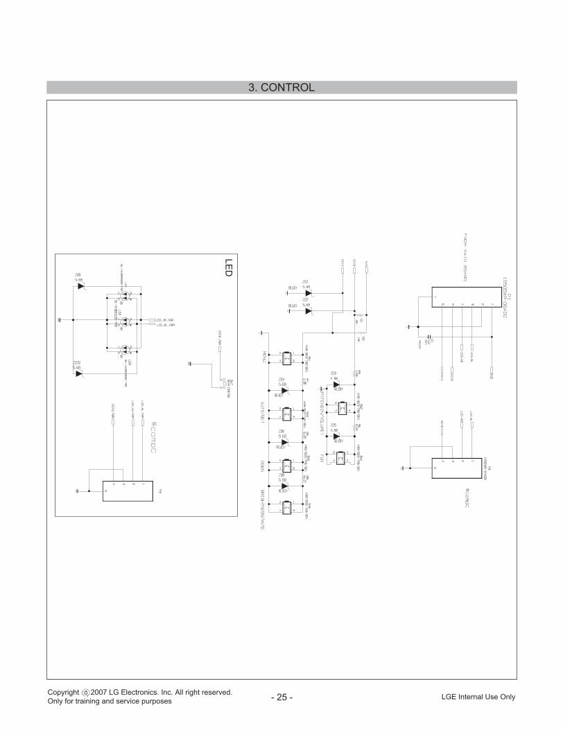
- 25 -
3. CONTROL
Copyright 2007 LG Electronics. Inc. All right reserved.Only for training and service purposes LGE Internal Use Only
LED
Nov. 2007P/NO : MFL30290861 Printed in China
![Prefeitura Municipal de Carlos Barbosa · 002.016.007 00007290.000 monitor 17' lcd marca lg, modelo flatron w1752t na cor preta. 413,10 bom [ ] 002.016.007 00011778.000 monitor marca](https://img.pdfslide.net/doc/110x75/5eb29f4c47d8df2c6f71b263/prefeitura-municipal-de-carlos-002016007-00007290000-monitor-17-lcd-marca-lg.jpg)


![LG Flatron LCD Monitor L1512S Service Manual[1]](https://img.pdfslide.net/doc/110x75/553ede60550346096e8b463b/lg-flatron-lcd-monitor-l1512s-service-manual1.jpg)