Embed Size (px)
Citation preview
IEEE TRANSACTIONS ON ELECTRON DEVICES, VOL. ED-21, NO. 9, SEPTEMBER 1980 1733
Limitations of Multilevel Storage in Charge- Coupled Devices
HODA S . ABDEL-ATY ZOHDY, MEMBER, IEEE, SAWAS G. CHAMBERLAIN, SENIOR MEMBER, IEEE, AND LYNN A. K. WATT, SENIOR MEMBER, IEEE
Abstract-The feasibility of applying multilevel storage (MLS) in charge-coupled devices (CCD’s) is demonstrated in this paper. The effect on the allowable number of levels of the different noise sources in the CCD, the input-signal power, the charge-handling capacity, and the effective bandwidth have been considered. Accurate noise measure- ments, by means of statistical correlation are presented. With eight levels of charge, three bits of data have been achieved in one storage cell with two-phase stepped-oxide double-polysilicon CCD’s, and detected with an average error probability of 2 X 10-lo. Four bits of data in one storage cell could be achieved in similar devices with a charge-transfer inefficiency of E < 1 X with an average error probability of less than 9 X IO-*.
L 2. INTRODUCTION
ARGE-SCALE MEMORIES are among the significant applications of charge-coupled devices (CCD’s). In terms
of cost performance, CCD memories are comparable to the magnetic bubble memories (MBM), and offer an edge of pro- viding better yield and less access time than MBM’s [ 11 -[3] .
Lin and Mattson [4] have shown that multilevel storage in shift registers improves the access time as well as the cost per bit over a two-level storage system. Multilevel storage in CCD’s is a way of achieving smaller areas per bit in memory applica- tions while leaving the basic technology and device organiza- tion as well as the latency time unchanged [ 11 . The feasibility of storing more than two levels in a CCD shift-register cell is limited by the charge-handling capacity, which depends on the storage gate physical dimensions, clocking and biasing condi- tions, the necessary voltage separation between adjacent levels, the parameter tolerance and variations in the circuits used to supply the references, and the allowable transmission capacity, which is a function of the transfer inefficiency (e) and the total number of transfers (p).
This paper reports the results of an investigation of the limit- ations on multilevel storage in surface-channel CCD’s. Using a two-phase stepped-oxide CCD, analytical methods are em- ployed along with experimental measurements to determine the feasible number of levels for a predetermined detection error probability. Thle effect of each of the noise sources in the CCD on the feasible number of levels is examined both analytically and experimentally.
Manuscript received August 20, 1979; revised February 12, 1980. This work was supported by a research grant from the Natural Sciences and Engineering Research Council of Canada, under Grants A7383 and A3669.
The authors are with the Department of Electrical Engineering, Uni- versity of Waterloo, Waterloo, Ont., Canada, N2L 3G1.
A theoretical analysis of the dependence of the charge-han- dling capability on the allowable gate voltage swing, the tech- nology used, and the gate area is presented in Section 11. Ex- pressions for the allowable voltage step size for a predetermined number of levels as a function of the different noise sources in the CCD, the allowable peak-to-peak signal voltage, the possible detection error, and the signal-to-noise power ratio are given in Section 11. The transmission capacity of the CCD as a func- tion of the effective bandwidth, assuming that the time interval required to allow the transmitted levels to be recognized indi- vidually at the output is similar to that of an ideal filter, is also given in Section 11.
The method used for noise measurements is discussed in Section 111. This includes a theoretical analysis of the correla- tion method, a description of the circuit along with the re- quired calibration steps and measurements of the experimental system transfer function G ( f ) , and the CCD shift register input-to-output transfer function H ( f ) .
Experimental results are reported in Section IV for n-chan- ne1 two-phase double-polysilicon stepped- oxide CCD shift registers with 36 transfer gates. Noise measurements for dif- ferent charge packet sizes and different sources in the CCD are presented and investigated. Also, an improved technique for signal-charge insertion using the surface-potential equilibra- tion method, which was used for the experimental measure- ments, is presented.
Combining the experimental results with the theoretical ex- pressions, the predicted limitations for multilevel-storage (MLS) applications have been calculated in Section IV.
11. THEORY FOR MULTILEVEL STORAGE The MLS structure in a CCD consists of three basic sections
[5], [6] : the input insertion section, the CCD shift register with MLS, and the output sensing section. Each of these sec- tions must be considered separately in examining the feasibility of MLS in CCD’s. For a CCD memory block with MLS, there should also be a digital-to-analog (D/A) converter unit at the input and an analog-to-digital (A/D) converter unit at the out- put. The feasibility of storing more than two-levels in a CCD cell is determined by the charge-handling capability in the device, the allowable voltage step size between adjacent levels, and the allowable transmission capacity, which is limited by pe as well as the tolerances and variations in the circuit param- eters. In this section, an expression for the charge-handling capacity in the device is given in terms of the maximum allow- able storage-gate voltage-swing and the storage-unit parameters.
0018-9383/80/0900-1733$00.75 0 1980 IEEE
The allowable range for the voltage separation be.tNreen adjzl- cent levels is given as a function of the clock operating fre- qu~:mcy, the maximum allowable gate-voltage ,swing, the dif- ferent noise sources in the CCD, the average signal power, the required number of storage levels, and the possible detection error. An expression is also given in this section for the possible number of bits per bucket.
A. Charge-Handling Capacity The allowable number of storage levels in a CCD shift register
is strongly dependent on the charge-handling capacity oif the indlividual storage units. In dynamic Operation, the storage- un:it capacitance is effectively the parallel combination olf the indlividual gate-oxide capacitance and the 'depletion capaci- tance; usually the gate-oxide capacitance per unit area is much greater than the depletion capacitance per unit area. Thus the capacity for charge storage may be significantly enhanced by inaeasing the depletion capacitance in the storage-gate region [7] or by increasing the storage-gate area.
The charge-handling capacity of the storage unit is also pro- portional to the gate-voltage swing, which is ultimately limited by either the surface avalanche breakdown 0.1 the oxide break- down [8]. In lightly doped junctions, the avalanche break- down voltage imposes an upper limit on the reverse gate volt- age since the multiplication effects dominate the breakdown mechanism. The avalanche multiplication region is consi'dered when the multiplication factor is 2 6 [9] . 'Thus a maximum voltage of [(0.833)'/n VBD - lV&l] can be used without avalanche breakdown where V& is the substrate bias, ViBD is the breakdown voltage, and n is 2 when the avalanche is d.ue to electrons.
For the Si-SiOz interface, the field in the silicon at avalanche breakdown is 5 X lo5 V/cm, while the corresponding field in the insulator is approximately three times larger [ lo] . Thus the maximum allowable potential difference across the oxide is 1.5 X lo6 to, and therefore
(V, - &) < 1.5 x lo6 to, (1)
where to, is the oxide thickness in centimeters and V, is the gate applied voltage. The surface potential GS is given by [ 111
r& = v;: -I- v, - ( 2 v;: v- -I- v ; p (2)
where V& = V, t IV& I - VFB - V,, ViB = qNA es/CLz, V, is the effective signal voltage, V,, is the flat-band voltage, and CA is the oxide capacitance per unit area, es is the permittivity of the substrate, and NA is its doping. Equations (1) and ( 2 ) will give an upper limit for the effective signal voltage. For a two-phase stepped-oxide device in the complete charge-transfer mode of operation there is another limit on the allowable signal-voltage swing which is determined by the built-in barrier height. This limit can be approximated as the difference be- tween Vh and V , the threshold voltages of the thick and thin oxide gates. The smallest of these limits will be the maximum allowable signal-voltage swing Vpp. The maximum charge which can be handled with the device is Vpp (C, + C D ) where C, and C, are the oxide and depletion-layer capacitances. Thus the maximum charge-handling capacity is linearly propor- tional to the area of the storage gate.
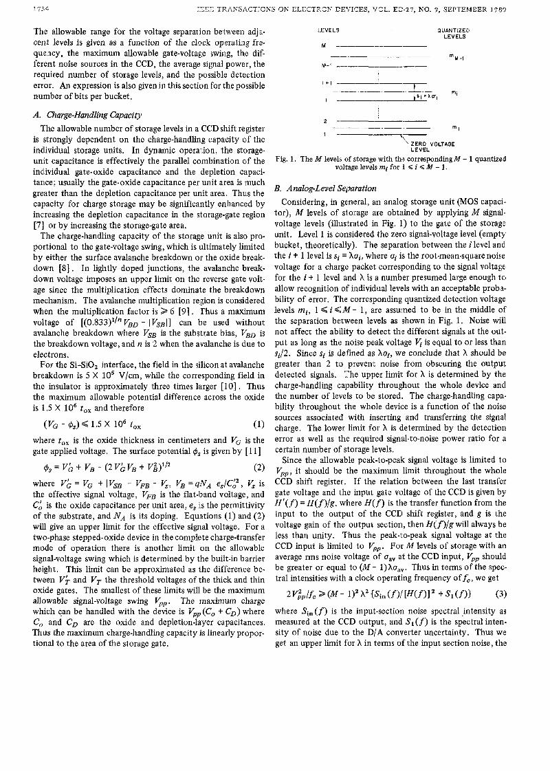
L.E\/E LS QUANTIZED LEVELS
M
-- ~ m M - l M - I ________-___ j + 1 ----L-
i x;ri mi
2
1 ----- m l 7-
'ZERO VOLTAGE LEVEL
Fig. 1. The M level;, alf storage with the corresponding M - 1 quantizedl voltage levels mi for 1 < i 4 M -- 1.
B. Analog-Level 2ieparation Considering, in general, an analog storage unit (MOS capad..,
tor), M levels of storage are obtained by applying M signal.., voltage levels (illwtrated in Fig. 1) to the gate of the storage unit. Level 1 is considered the zero signal-voltage level (empty bucket, theoreticd1y)l. The separation between the i level and. the i + 1 level is si = h q , where ai is the root-mean-square noise voltage for a charge packet corresponding to the signal voltage; for the i t 1 level and X is a number presumed large enough to allow recognition of individual levels with an acceptable probrsr bility of error. The! corresponding quantized detection voltage levels mi, 1 < i S l M - 1, axe assumed to be in the middle of the separation between levels as shown in Fig. 1. Noise will not affect the ability to detect the different signals at the oub put as long as the noise peak voltage 6 is equal to or less tham s i /2 . Since si is deihed as hat, we conclude that h should be greater than 2 tmo prevent noise from obscuring the output detected signals. The upper limit for h is determined by the: charge-handling capability throughout the whole device and the number of levels to be stored. The charge-handling capa- bility throughout the whole device is a function of the noise: sources associated with inserting and transferring the signal charge. The lower limit for h is determined by the detection error as well as thle required signal-to-noise power ratio for a certain number of storage levels.
Since the allowable peak-to-pealk signal voltage is limited to Vpp, it should be the maximum limit throughout the whole CCD shift register. If the relation between the last transfer gate voltage and the input gate voltage of the CCD is given by H ' ( f ) = H ( f ) / g , where H ( f ) is the transfer function from the input to the output of the CCD shift register, and g is the voltage gain of the output section, then H ( f ) / g will always be less than unity. Thus the peak-to-peak signal voltage at the CCD input is limited to Vpp. For M levels of storage with an average rms noise voltage of u, a d the CCD input, Vpp should be greater or equal to (M - l)ho,,. Thus in terms of the spec- tral intensities with a clock operating frequency off,, we get
2V&/fc 2 (M - 1)' h2 {Sin (fX [H(f)I + S1 (f)) (3)
where Si,(f) is the input-section noise spectral jntensity as measured at the CCD output, and Sl(f) is the spectral inten- sity of noise due to the D/A converter uncertainty. Thus we get an upper limit for h in terms of the input section noise, thle
ZOHDY et al.: MULTILEVEL STORAGE IN CCD’s 1735
charge-handling capacity, and the required number of storage levels. Characterization of the input-section noise is essential t o improve h as given by (3) and thus reduce the possible de- tection error and error probability, as will be shown later.
Also, since the maximum allowable signal voltage at the last transfer electrode is limited by V p p H r ( f ) , then if the CCD is to be used with M levels of storage an upper limit for h is set by the relation
2 v . p [ ~ ‘ ( f ) 1 2 / f c > ( M - V h 2 {Sl(f)[H’(f)l2 ’. [S3(f) - s o ” , ( f ) l / g 2 ) . (4)
In (4), S 3 ( f ) is the overall noise spectral intensity in the CCD, which is a function of the charge-packet size as well as the wave-analyzer frequency, and SOut(f) is the output-section noise spectral intensity measured at the CCD output. Compar- ing (3) and (4), it is clear that (4) gives the upper limit for h if the charge packets are to be within the handling capability for Mlevels of storage throughout the entire device.
For the M - 1 quantized levels given in Fig. 1 as mi for 1 < i < M - 1, the detection error will be m(t ) - mi if the signal level is m(t) . If F(m)dm is the probability that m(t ) lies in the voltage range m k dm/2, then the mean-square detection error will be
Assuming that the probability density function is constant within each quantization range [ 1 2 ] , i.e., F(m) = Fi, a con- stant, for 1 < i < M - 1 , we get
- M-1 e’ = Fi(h0i)3/12.
i=l
Since Fi(hai) is the probability that the signal voltage m(t ) lies in the i quantization range, then
M - 1 F i ( h ~ i ) = 1 .
i = l
For simplicity, we assume equal spacing between thelevels,i.e., sl = s2 = SM-1 = huM-l = s, where aM-l is the noise rms voltage for the charge packet associated with the M level. The rms noise voltage in CCD’s increases with increasing the charge- packet size, as will be shown in the results. Thus we can say that
OM-1 > 0M-2 ’ ‘ ’> (71 (6 )
and we get a relation between the required spacing and the mean-square detection error as - e2 < s2/12. (7)
For a CCD memory block with M U , the overall detection- noise voltage-spectral intensity S,(f) at the output of the CCD is given as
S,(f) = Sl(f) [Wf)l + &(f> + S3(f) (8)
where S 2 ( f ) is the noise spectral intensity due to the output A/D converter uncertainty. From (7), (8), and the fact that
the noise rms voltage is given as 112
(9)
we get a lower limit for the required separation between adja- cent levels
( 1 0)
where S‘ = h a ~ - ~ H ( f ) . The separation between adjacent levels is also a function of
the signal-to-noise power ratio for a given number of storage levels. Suppose that the M levels are represented by M fixed voltages and that the levels at the input have been separated by the intervals ha l , Xuz, , huM-l where ui is the noise rms voltage at the input of the CCD for the it 1 charge packet. If we assume that the M levels occur with equal likelihood, then the average signal power will be
(1 1 ) From (6) and ( 1 1) we get P, < h2 u&-,(M - 1) (2M - 1 ) / 6 which gives a lower limit for h for a given signal-to-noise input power ratio and M levels of storage. In practice, the lower limit for X is determined by the signal-to-noise power ratio as long as the number of storage levels is less than a number we denote by M1, which is a solution of (13) below. If the num- ber of levels exceeds M1, then the lower limit for X is deter- mined by the mean-square detection error. Thus we have
and M1 is obtained by solving the equation
P,/[(Ml - 1 ) OM1 - 111 = 2 [lfci2 {Sl ( f> [Wf)12
t S2 (f) t S3 (f)) d f / [H(f)l *
(13)
I From the previous equations, it can be seen that for a given
signal-to-noise power ratio the number of storage levels per
I736 iEEE TRANSACTIONS ON ELECTRON DEVICES, VOL. ED-27, NO. 9, SEPTEMBER 1980
TABLE I - __ VARIABLE RANGE OF
LEVEL M ALLOWABLE NUMBER OF
MEAN SQJARE UPPER L I M I T DETECTI'IN FOR E=(M-l)A
- LEVELS ERROR
average signal unlimited Increasing the
increased unaffected power
increased
Decreasing the input section unlimited increased decreased increased noise
Decreasing the transfer section M < Mi noise
unaffected decreased increased
M 1 M1 increased decreased increased Decreasing the output section < M1 noise
unaffected decreased unaffected
M 2 MI increased decreased unaffected
bucket (M,) is
M,= 1 4 [3 t (l t-YZ].
Defining a quality parameter 0 as the ratio of the allowable number of levels to the probability of detection error, then 0 will be proportional to (M - 1)h. From (12) we can deduce that p will not be changed by reducing the output-section noise, but it will be increased by reducing the input-section noise and/ or the transfer-process noise. The effects of the different noise sources and the average signal power on the number of levels and the possible detection error are summarized in Table I along with their effects on 0.
C. The Transmission Capacity To find the information rate of the signals, we have to esti-
mate the interval T which should be assigned to each bucket in order to allow the transmitted levels to be recognized in- dividually at the output. In practice, when the input signals are in the form of abrupt steps, T can be approximated by 0.44/B [12] where B is the effective bandwidth. According to Shannon's sampling theorem, the maximum bandwidth a charge-transfer device can have is fJ2. However, as given in [13] , incomplete charge transfer reduces the effective band- width of a CCD to B = (fc/2) exp {-2pe) 10(2pe), where 10(2pe) is a Bessel function of the first kind, E is the charge- transfer inefficiency of the device, and p is the total number of transfers. Taking T = 0.44/B, there will be 2.278 bucketsls, and the transmission capacity in bits per second will be
c ~ = 2 . 2 7 B { - 2 t l o g ~ [ 3 t (1 t-r']}. (15)
Since the time required for transferring the charge from one stage of the shift register to the next is l/fc, then the number of transferring bits per bucket will be
111. EXPERIMENTAL MEASURING CIRCUIT The correlation method was chosen for noise measurements
throughout this work. This method has the following proper- ties: 1) it is well suited for measuring low levels of electrical noise [14], 2) the output signal pulses and the accompanying
- SWEEP -
Y I t
0.5. l o M H z WAVE ANALYZER
..
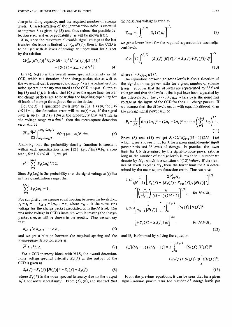
Fig. 2. (a) The experimental measuring circuit for noise measurements by the correlation method. A multiplier, type MC1595, is used with a scale factor of 0.15. An RC averaging circuit is used with a timecon- stant of 0.12 ms such that the thermal noise of 52-sl resistance can be detected with this measuring circuit. An RC integrator is used for smoothing the wave analyzer output with R = 1.5 ksl and C = 2 mF. (b) A detailed circuit of the amplifier and low-pass filter (AMP &LPF), which gives a midband voltage gain of 1.55 and a bandwidth of 100 kHz.
small clock pulses from the CCD under test can be separated from the noise by adjustment of the circuit parameters, and 3) a long-time averaging circuit can be used to attenuate the noise generated within the measuring circuit as well as to improve the measuring sensitivity [14] .
One of the first circuits developed to study the correlation between two signals was that of Brown and Twiss [ 151. Anal- ysis of this circuit has been presented [14] for small-signal measurements where the desired noise signal was considered to be the only output from the device. Throughout our anal- ysis, the output from the CCD terminal is considered to be the sum of three components p ( t ) t u(t) + c(t) , where p ( t ) is the output signal, u(t) is the noise (to be measured), and c( t ) represents small output pulses at the clock-operating frequency.
A. Theory The circuit configuration for our noise measurements by the
correlation method is given in Fig. 2. The output of the CCD is connected to two separate channels consisting of amplifiers with gains al and az . The corresponding noise signals of the amplifiers are u1 (t) and uz (t). Each of the channels has a low- pass filter to minimize the amplitude of the clock pulse com- ponents, and also to restrict the noise power actually passed to the wave analyzer. The outputs from the two channels are fed into the cross correlator which consists of a delay element in channel number 2, a multiplier for the outputs of the two channels, and an averaging circuit. The output from the filters of the two channels is given byX1 (i) = a l p (t) t al u(t) + ul (t), and X z ( t - td ) =azp ( t - td) t azu(t - td) t uz(t) , where td is the time delay in the delay element. The output from the multiplier is given by X l ( t ) X 2 ( t - td), and the output after the averaging circuit is
X1 (t)Xz (t - td) = average of [ala2p ( t ) p (t - t d )
alazu(t)u(t - t d ) l (1 7)
ZOHDY et al.: MULTILEVEL STORAGE IN CCD's 1737
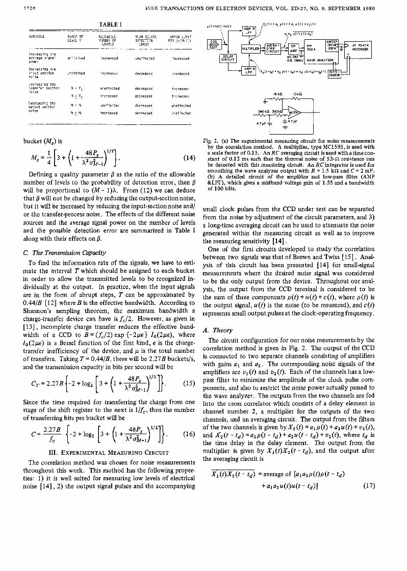
- p ( 1 p ( t - t d ) -
td 120- 3b 5 t d d -Tdk z E z 100-
Fig. 3. The CCD output signal p ( t ) , as well as the part p ( t ) p ( t - t d ) of 80 -
the multiplier output, versus the delay time td for a signal frequency of 1/T1 and a signal pulsewidth of T z . 5 60-
2
LOW FREOUENCY MEASURING CIRCUIT GAIN
B
since ul(t), u,(t), u(t), and p(t) are not correlated with each other.
From (17), p(t)p(t -y) has to be eliminated from the noise measurements. This can be achieved if the time delay ( t d ) of the cross correlator lies in the range Tz < td < T1 - T z , as shown in Fig. 3, where T1 is the signal pulse period, and Tz is the signal pulsewidth. ~ In this case, the output from the cross correlator will be alaz u(t)u(t - td).
B. Calibration To measure the noise spectral intensity by the above correla-
tion circuit, the output from the cross correlator was connected to a 302A HP wave analyzer with a 6-Hz noise bandwidth. The wave analyzer measured the spectral voltage levels through a long time-constant integrator by means of the Hp 7047 x-y recorder, which gave the measurements in volts per Hz1I2. In our measuring circuit, a 16-bit CCD shift register at 1.2-MHz clock rate provided the necessary delay of 15 ps. A signal fre- quency of 30 kHz with a signal pulsewidth of 3.3 ps was used. In general, 16-bit CCD's can be used as delay elements for delay times td > 11 ps.
All the noise measurements in this work are referred to the output of the CCD, i.e., the noise measurements are given as the x-y recorder reading divided by the transfer function of the measuring circuit G ( f ) . The transfer function G ( f ) was measured by using carbon resistors and a noise generator. With a carbon resistor as the noise source, G ( f ) was determined by dividing the measured output by the theoretically expected spectral voltage level for a 1-Hz bandwidth ((4KTR)'/'). The output measurements agree with the theoretically expected results in the frequency range f = 5-8 kHz. Experimental re- sults for the measuringcircuit transfer function are given in Fig. 4. The circuit calibration shows that the possible error in noise measurements is less than 7.7 percent.
F 401 20
O--O MEASURED USING A RANDOM NOISE GENERATOR
W MEASURED USING A 1 0 0 Mn CARBON RESISTOR
I I + I I I I I I I I I * 0 5 10 15 20 25 30 35 40 45 50
WAVE ANALYZER FREQUENCY ( k H z )
Fig. 4. The transfer function G ( f ) of the noise-measuring circuit.
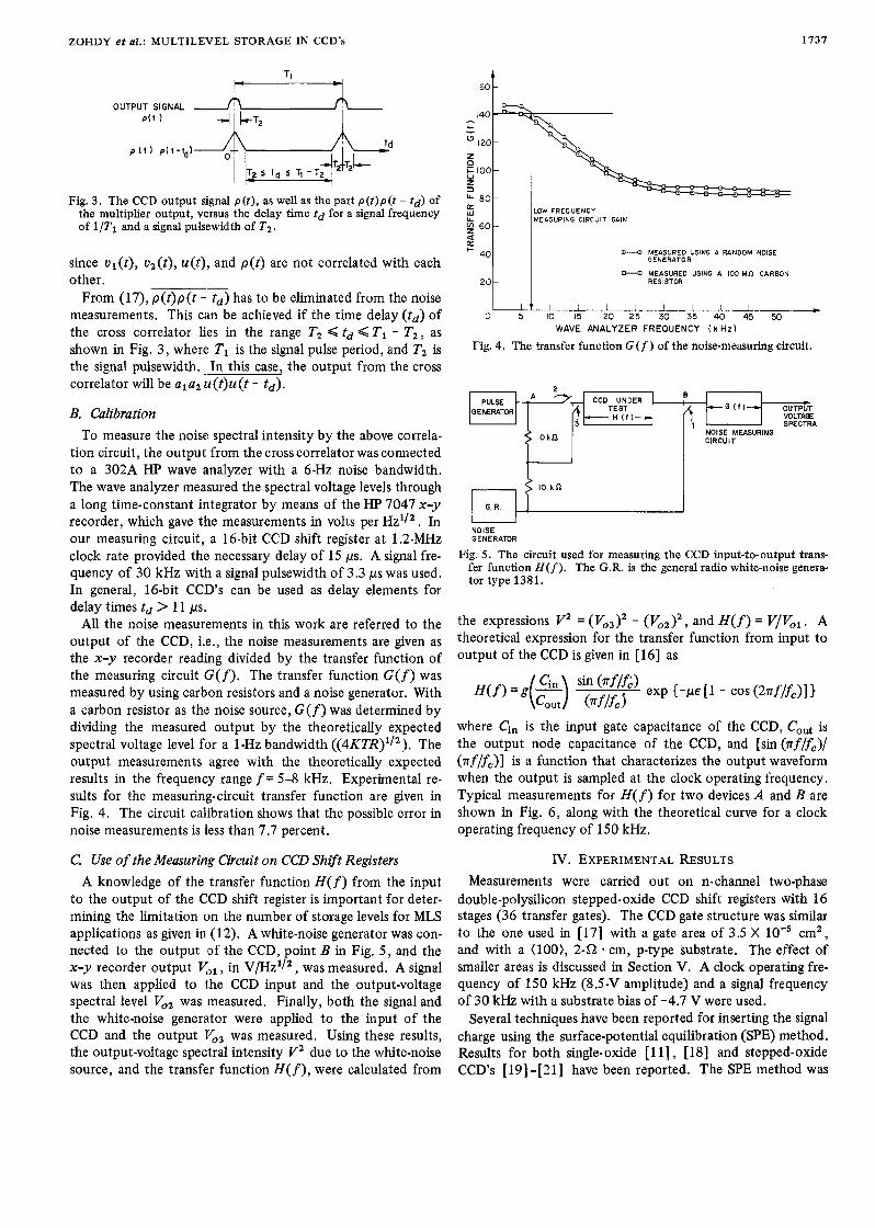
I ' NOISE MEASURING CIRCUIT
t---l I
NOISE GENERATOR
Fig. 5. The circuit used for measuring the CCD input-to-output trans- fer function H ( f ) . The G.R. is the general radio white-noise genera- tor type 1381.
the expressions V z = (V,,)' - (V,,)', and H ( f ) = V/Vo,. A theoretical expression for the transfer function from input to output of the CCD is given in [ 161 as
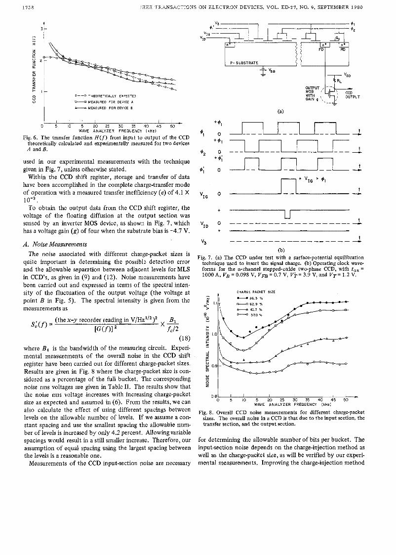
where Ci, is the input gate capacitance of the CCD, Gout is the output node capacitance of the CCD, and [sin (nf/fc)/ (nf/fc)] is ;L function that characterizes the output waveform when the output is sampled at the clock operating frequency. Typical measurements for H(f) for two devices A and B are shown in Fig. 6, along with the theoretical curve for a clock operating frequency of 150 kHz.
C. Use of the Measuring Circuit on CCD Shift Registers IV. EXPERIMENTAL RESULTS A knowledge of the transfer function H ( f ) from the input
to the output of the CCD shift register is important for deter- mining the limitation on the number of storage levels for MLS applications as given in (12). A white-noise generator was con- nected to the output of the CCD, point B in Fig. 5, and the x-y recorder output Vol , in V/Hz1I2, was measured. A signal was then applied to the CCD input and the output-voltage spectral level Voz was measured. Finally, both the signal and the white-noise generator were applied to the input of the CCD and the output Vo3 was measured. Using these results, the output-voltage spectral intensity V z due to the white-noise source, and the transfer function H ( f ) , were calculated from
Measurements were carried out on n-channel two-phase double-polysilicon stepped-oxide CCD shift registers with 16 stages (36 transfer gates). The CCD gate structure was similar to the one used in [I71 with a gate area of 3.5 X lo-' cm', and with a (loo), 242 * cm, p-type substrate. The effect of smaller areas is discussed in Section V. A clock operating fre- quency of 150 kHz (8.5-V amplitude) and a signal frequency of 30 kHz with a substrate bias of -4.7 V were used.
Several techniques have been reported for inserting the signal charge using the surface-potential equilibration (SPE) method. Results for both single-oxide [ll] , [I81 and stepped-oxide CCD's [19] -[21] have been reported. The SPE method was
17?8 : Z Z E TRANSACTTONS ON ELECTRON DEVICES, VOL. ED-27, NO. 9, SEPTEMBER 1.980
i P- SUBSTRATE
n u u
O--O THEORETICALLY EXPECTED
M MEASURED F O R DEVICE A - MEASURED FOR D N l C E B
I i i I i 1 : 0 5 IO 15 20 25 30 35 40 45 50
1 1 i _i
WAVE ANALYZER FREQUENCY ( k H z )
Fig. 6 . The transfer function H ( f ) from input to output of the CCD theoretically calculated and experimentally measured for two devices A and B .
used in our experimental measurements with the technique given in Fig. 7 , unless otherwise stated.
Within the CCD shift register, storage and transfer of data have been accomplished in the complete charge-transfer mode of operation with a measured transfer inefficiency ( E ) of 4.1 X
To obtain the output data from the CCD shift register, the voltage of the floating diffusion at the output section was sensed by an inverter MOS device, as shown in Fig. 7, which has a voltage gain (g) of four when the substrilte bias is -4.7 V.
10-3.
A. Noise Measurements The noise associated with different charge-packet sizes is
quite important in determining the possiblle detection error and the allowable separation between adjacent levels for MLS in CCD's, as given in (9) and (12). Noise measurements have been carried out and expressed in terms of the spectral inten- sity of the fluctuation of the output voltage (the voltage at point B in Fig. 5). The spectral intensity .is given from the measurements as
(the x-y recorder reading in V/Hzl/')' B1 SXf) =
[G(f 11 X -
f C l 2 (1 8)
where B 1 is the bandwidth of the measuring circuit. Experi- mental measurements of the overall noise in the CCD shift register have been carried out for different charge-packet sizes. Results are given in Fig. 8 where the charge-packet size is con- sidered as a percentage of the full bucket. 'The corresponding noise rms voltages are given in Table 11. The results show that the noise rms voltage increases with increasing charge-packet size as expected and assumed in (6). From the results, we can also calculate the effect of using different spacings between levels on the allowable number of levels. If we assume a con- stant spacing and use the smallest spacing the allowable num- ber of levels is increased by only 4.2 percent. Allowing variable spacings would result in a still smaller increase. Therefore, our assumption of equal spacing using the largest spacing between the levels is a reasonable one.
Measurements of the CCD input-section noise are necessary
4; 0 t
--c
VID 0 + U t .-c
+
v3 t ------------------- -
(b) Fig. 7. (a) The CCD under test with a surface-potential equilibration
technique used to insert the signal charge. (b) Operating clock wave- forms for the n-channel stepped-oxide two-phase CCD, with tOx = ~ O O O A , V B = ~ . O ~ ~ V , V ~ , = O . ~ V , V + = ~ . ~ V , ~ ~ ~ V T = ~ . ~ V .
A CHARGE PACKET SIZE
- 9 6 . 3 %
E--a 62.9 % - 40.7 % - 37.0%
0.8 I I I I I I I I I C 0 5 IO 15 20 25 30 35 40 45 50
WAVE ANALYZER FREQUENCY (kHz)
Fig. 8. Overall CCD noise measurements for different charge-packet sizes. The overall noise in a CCD is that due to the input section, the transfer section, and the output section.
for determining the allowable number of bits per bucket. The input-section noise depends on the charge-injection method as well as the charge-packet size, as will be verified by our experi- mental measurements. Improving the charge-injection method
ZOHDY et al.: MULTILEVEL STORAGE IN CCD's
- o,6 I DYNAMICALLYINTRODUCED 1 U OPTICALLY INTRODUCED , ll USING THE SURFACE PDTrmTlAL EQUILIBRATION TECHNIQUE
0 0 5 OF FIG. 7 TO
05 1
1739
WAVE ANALYZER FREQUENCY ( k H z )
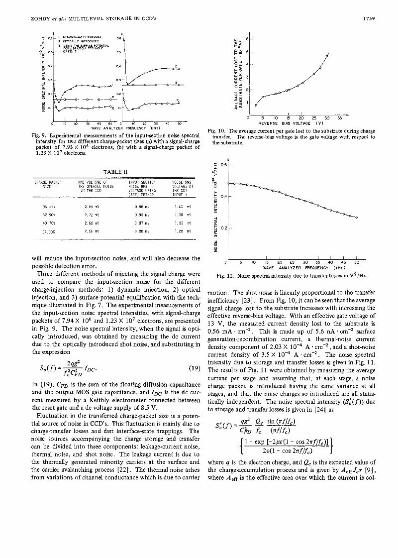
Fig. 9. Experimental measurements of the input-section noise spectral intensity for two different charge-packet sizes (a) with a signal-charge packet of 7.93 X lo6 electrons, (b) with a signal-charge packet of 1.23 X lo7 electrons.
TABLE I1
CHARGE PACKET RMS VOLTAGE OF INPUT SECTION NOISE RMS THE OVERALL NOISE NOISE RMS
VOLTAGE USING VOLTAGE AT
I?PF\ MFTunn THE CCD INPI IT n
S I Z E I N THE CCD
1 , I I I I ) 0 5 IO 15 20 25 30 35
REVERSE BIAS VOLTAGE L V )
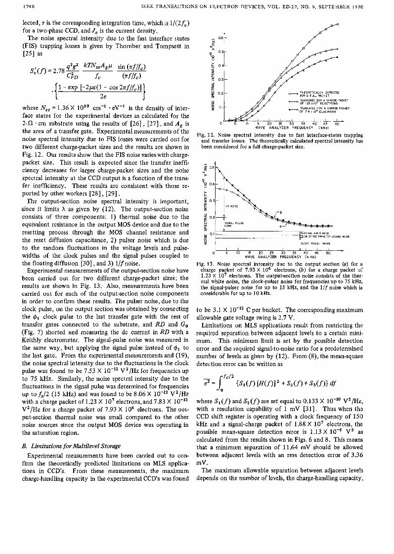
Fig. 10. The average current per gate lost to the substrate during charge transfer. The reverse-bias voltage is the gate voltage with respect to the substrate.
3 0.6
N' >
9 6 . 2 9 % 2 . 8 0 mV 0.98 mV 1.40 mV
6 2 . 9 0 % 2 . 7 2 mV 0.95 mV 1.38 mV
40.70% 2 . 6 8 mV 0.87 mV 1.33 mV
37.00% 2 . 5 8 mV 0.80 mV 1.28 mV
will reduce the input-section noise, and will also decrease the possible detection error.
used to compare the input-section noise for the different
0
Three different methods of injecting the signal charge were pig. 11.
5 IO 15 20 25 30 35 40 45 50 WAVE ANALYZER FREQUENCY ( k H z )
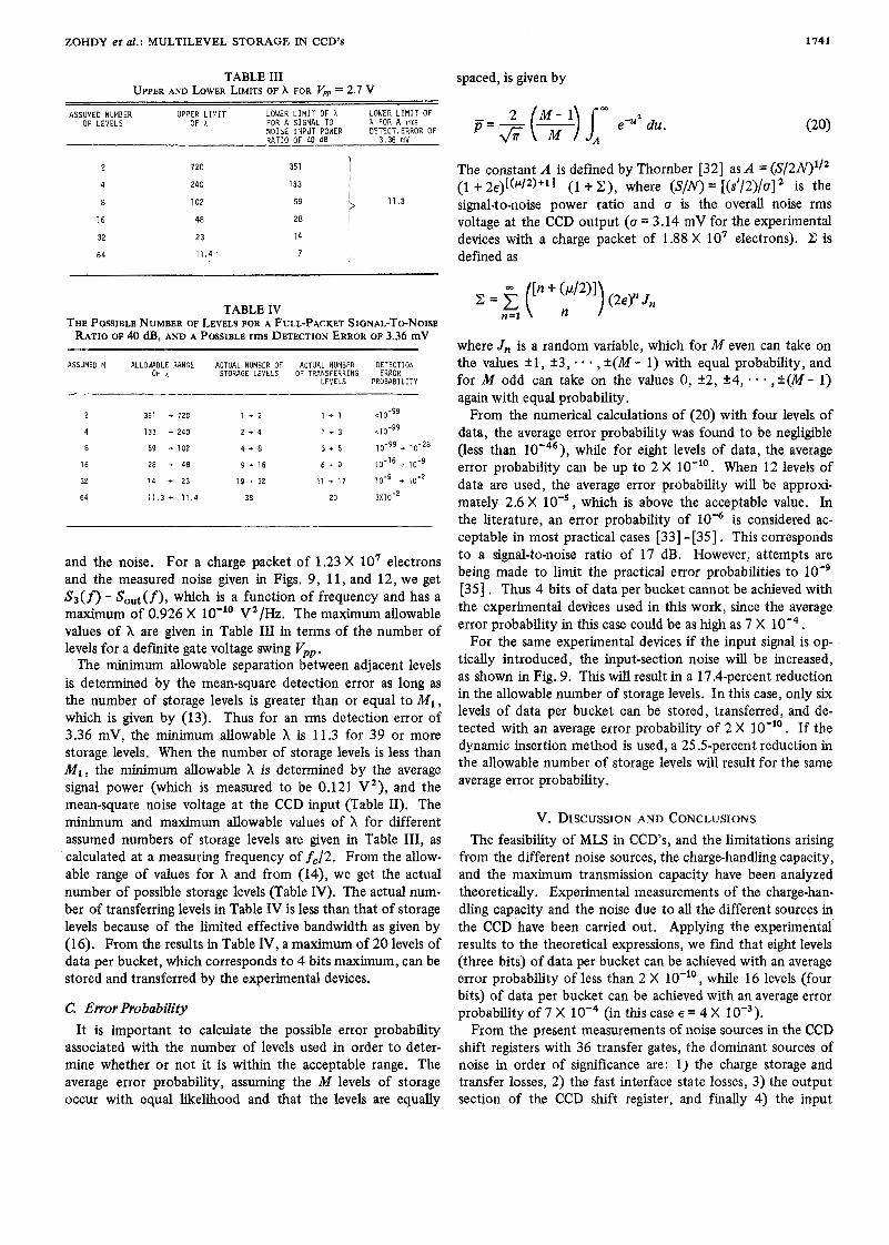
Noise spectral intensity due to transfer losses in V2/Hz.
charge-injection methods: 1) dynamic injection, 2) optical injection, and 3) surface-potential equilibration with the tech- nique illustrated in Fig. 7 . The experimental measurements of the input-section noise spectral intensities, with signal-charge packets of 7.94 X IO6 and 1.23 X lo' electrons, are presented in Fig. 9. The noise spectral intensity, when the signal is opti- cally introduced, was obtained by measuring the dc current due to the optically introduced shot noise, and substituting in the expression
In (19), CFD is the sum of the floating diffusion capacitance and the output MOS gate capacitance, and IDc is the dc cur- rent measured by a Keithly electrometer connected between the reset gate and a dc voltage supply of 8.5 V.
Fluctuation in the transferred charge-packet size is a poten- tial source of noise in CCD's. This fluctuation is mainly due to charge-transfer losses and fast interface-state trappings. The noise sources accompanying the charge storage and transfer can be divided into three components: leakage-current noise, thermal noise, and shot noise. The leakage current is due to the thermally generated minority carriers at the surface and the carrier avalanching process [22] . The thermal noise arises from variations of channel conductance which is due to carrier
motion. The shot noise is linearly proportional to the transfer inefficiency [23] . From Fig. 10, it can be seen that the average signal charge lost to the substrate increases with increasing the effective reverse-bias voltage. With an effective gate voltage of 13 V, the measured current density lost to the substrate is 0.56 mA * cm-' . This is made up of 5.6 nA cm-' surface generation-recombination current, a thermal-noise current density component of 2.03 X A * cm-' , and a shot-noise current density of 3.5 X A * cm-' . The noise spectral intensity due to storage and transfer losses is given in Fig. 1 1 . The results of Fig. 1 1 were obtained by measuring the average current per stage and assuming that, at each stage, a noise charge packet is introduced having the same variance at all stages, and that the noise charges so introduced are all statis- tically independent. The noise spectral intensity (S:( f)) due to storage and transfer losses is given in [24] as
1 - exp [-2pe(l - cos 2nf/fc)] .I 2 4 1 - cos 2.f/fc)
where 4 is the electron charge, and Q, is the expected value of the charge-accumulation process and is given by A e ~ J e 7 [ 9 ] , where A,ff is the effective area over which the current is col-
1740 IEEE TRANSACTIONS ON ELECTRON DEVICES, VOL. ED-27, NO. 9, SEPTEMBER 1 9 8 ~
lected, 7 is the corresponding integration time, whichis l / j2 f,) for a two-phase CCD, and Je is the current density.
The noise spectral intensity due to the fast interface states (FIS) trapping losses is given by Thornber and Tompse:tt in [25] as
1 2E J where N,, = 1.36 X 10" cm-2 * eV-' is the density of inter- face states for the experimental devices as calculated for the 24'2 * cm substrate using the results of [26] , [27], and A, is the area of a transfer gate. Experimental measurements of the noise spectral intensity due to FIS losses were carried out for two different charge-packet sizes and the results are shown in Fig. 12. Our results show that the FIS noise varies with charge- packet size. This result is expected since the transfer ineffi- ciency decreases for larger charge-packet sizes and the noise spectral intensity at the CCD output is a function of the trans- fer inefficiency. These results are consistent with those re- ported by other workers [28], [29].
The output-section noise spectral intensity is important, since it limits h as given by (12). The output-section noise consists of three components: 1) thermal noise due to the equivalent resistance in the output MOS device and due to the resetting process through the MOS channel resistance and the reset diffusion capacitance, 2) pulser noise which is due to the random fluctuations in the voltage levels and pulse- widths of the clock pulses and the signal pulses coupled to the floating diffusion [30] , and 3) l/f noise.
Experimental measurements of the output-section noise have been carried out for two different charge-packet sizes; the results are shown in Fig. 13. Also, measurements have been carried out for each of the output-section noise components in order to confirm these results. The pulser noise, due to the clock pulse, on the output section was obtained by connecting the G1 clock pulse to the last transfer gate with the rest of transfer gates connected to the substrate, and RD and Go (Fig. 7) shorted and measuring the dc current in RD with a Keithly electrometer. The signal-pulse noise was measured in the same way, but applying the signal pulse instead of @1 to the last gate. From the experimental measurements and (19), the noise spectral intensity due to the fluctuations in the clock pulse was found to be 7.53 X lo-'' V2 /Hz for frequencies up to 75 kHz. Similarly, the noise spectral intensity due to the fluctuations in the signal pulse was determined for frequencies up to f,/2 (1 5 kHz) and was found to be 8.06 X lo-'' V'/Hz with a charge packet of 1.23 X lo' electrons, and 7.83 X lo-'' V'/Hz for a charge packet of 7.93 X lo6 electrons. The out- put-section thermal noise was small compared to the other noise sources since the output MOS device was operating in the saturation region.
B. Limitations for Multilevel Storage Experimental measurements have been carried out to con-
firm the theoretically predicted limitations on MLS applica- tions in CCD's. From these measurements, the maximum charge-handling capacity in the experimental CCD's was found
P
- THEORETICALLY EXPECTED FW A FULL PACKET
w k?
MEASURED FOR A CKARGE PACKET OF 123Xl0 ELECTRONS
g 01
0 5 10 15 20 25 30 35 40 45 50 W A V E A N A L Y Z E R F R E Q U E N C Y I k H z )
Fig. 12. Noise spectral intensity due to fast interface-states trapping and transfer losses. The theoretically calculated spectral intensity has been considered for a full charge-packet size.
O.;i., 0 A
0.1 - {THERMAL WHITE NOlOE I 3/36 O F ~ E T R A ~ F E R LOSSES N O ~ J E
CLOCK PULSE NOISE
l l l l l I l I 1 / - 0 5 10 15 20 25 30 35 40 45 50
WAVE ANALYZER FREQUENCY I k Hz1
Fig. 13. Noise spectral intensity due to the output section (u) for 21
charge packet of 7.93 X lo6 electrons, ( b ) for a charge packet of 1.23 X lo7 electrons. The output-section noise consists of the ther- mal white noise, the clock-pulser noise for frequencies up to 75 kHz, the signal-pulser noise for up t o 15 kHz, and the l/f noise which is considerable for up to 10 kHz.
t o be 3.1 X C per bucket. The corresponding maximum allowable gate voltage swing is 2.7 V.
Limitations on M U applications result from restricting the required separation between adjacent levels to a certain mini- mum. This minimum limit is set by the possible detection error and the required signal-to-noise ratio for a predetermined number of levels as given by (12). From (8), the mean-square detection error can be written as
2=Jfc'2 {Sl(f> [H(f>12 +S2(f)+S,(f)I&
where Sl(f) and S2(f) are set equal to 0.133 X lo-'' V2/Hz, with a resolution capability of 1 mV [31] . Thus when th'e CCD shift register is operating with a clock frequency of 150 kHz and a signal-charge packet of 1.88 X lo7 electrons, th'e possible mean-square detection error is 1.13 X V2 as calculated from the results shown in Figs. 6 and 8. This means that a minimum separation of 11.64 mV should be alloweld between adjacent levels with an rms detection error of 3.316 mV.
The maximum allowable separation between adjacent levels depends on the number of levels, the charge-handling capacity,
ZOHDY et al.: MULTILEVEL STORAGE IN CCD's 1741
TABLE I11 UPPER AND LOWER LIMITS OF A FOR GP = 2.7 V
spaced, is given by
ASSUMED NUMBER UPPER L I M I T LOWER L I M I T OF A LOWER L I M I T OF
NOISE INPUT POWER DETECT.ERROR OF RATIO OF 40 dB 3.36 mV
OF LEVELS OF A FOR A SIGNAL TO A FOR A rrns
2 720 3 5 1
4 2 4 0 1 3 3
8 1 0 2 59
1 6 48 2 8
32 23 1 4
64 11.4 7
I
J
> 11.3
TABLE IV
RATIO OF 40 dB, AND A POSSIBLE rms DETECTION ERROR OF 3.36 mV THE POSSIBLE NUMBER OF LEVELS FOR A FULL-PACKET SIGNAL-T~NOISE
ASSUMED I1 ALLOWABLE RANGE ACTUAL NUMBER OF ACTUAL NUMBER DETECTION OF h STORAGE LEVELS OF TRANSFERRING ERROR
LEVELS PROBABILITY
2 351 + 720 1 + 2 1 + 1 <10-99
4 1 3 3 + 240 2 - 4 1 + 3 <10-99
8 59 + 1 0 2 4 * 8 3 + 5 1 r g 9 + 1 o-28 1 6 2 8 + 4 8 9 + 1 6 6 - 9 10-16 + 10-9
32 14 * 23 1 9 + 32 11 + 1 7 1 0 - ~ +
6 4 1 1 . 3 * 1 1 . 4 3 8 20 3X10⁻²
and the noise. For a charge packet of 1.23 X lo7 electrons and the measured noise given in Figs. 9, 11, and 12, we get S 3 ( f ) - Sout(f), which is a function of frequency and has a maximum of 0.926 X lo-'' V2/Hz. The maximum allowable values of X are given in Table I11 in terms of the number of levels for a definite gate voltage swing Vpp.
The minimum allowable separation between adjacent levels is determined by the mean-square detection error as long as the number of storage levels is greater than or equal to M1, which is given by (13). Thus for an rms detection error of 3.36 mV, the minimum allowable X is 11.3 for 39 or more storage levels. When the number of storage levels is less than M I , the minimum allowable X is determined by the average signal power (which is measured to be 0.121 V2), and the mean-square noise voltage at the CCD input (Table 11). The minimum and maximum allowable values of X for different assumed numbers of storage levels are given in Table 111, as calculated at a measuring frequency of fJ2. From the allow- able range of values for A and from (14), we get the actual number of possible storage levels (Table IV). The actual num- ber of transferring levels in Table IV is less than that of storage levels because of the limited effective bandwidth as given by (1 6). From the results in Table IV, a maximum of 20 levels of data per bucket, which corresponds to 4 bits maximum, can be stored and transferred by the experimental devices.
C Error Probability It is important to calculate the possible error probability
associated with the number of levels used in order to deter- mine whether or not it is within the acceptable range. The average error probability, assuming the M levels of storage occur with equal likelihood and that the levels are equally
The constant A is defined by Thornber [32] as A = (S/~IV)'/~ (1 t 2e)[(p12)+1 I (1 t E), where (S /N) = [(s'/2)/cr] is the signal-to-noise power ratio and cr is the overall noise rms voltage at the CCD output (cr = 3.14 mV for the experimental devices with a charge packet of 1.88 X lo7 electrons). E is defined as
where Jn is a random variable, which for M even can take on the values +1, +3, , k(M - 1) with equal probability, and for M odd can take on the values 0, +2, +4, * , +(M - 1) again with equal probability.
From the numerical calculations of (20) with four levels of data, the average error probability was found to be negligible (less than while for eight levels of data, the average error probability can be up to 2 X lo-". When 12 levels of data are used, the average error probability will be approxi- mately 2.6 X which is above the acceptable value. In the literature, an error probability of is considered ac- ceptable in most practical cases [33] -[35]. This corresponds to a signal-to-noise ratio of 17 dB. However, attempts are being made to limit the practical error probabilities to lo-' [35] . Thus 4 bits of data per bucket cannot be achieved with the experimental devices used in this work, since the average error probability in this case could be as high as 7 X
For the same experimental devices if the input signal is op- tically introduced, the input-section noise will be increased, as shown in Fig. 9. This will result in a 17.4-percent reduction in the allowable number of storage levels. In this case, only six levels of data per bucket can be stored, transferred, and de- tected with an average error probability of 2 X 10-l'. If the dynamic insertion method is used, a 25.5-percent reduction in the allowable number of storage levels will result for the same average error probability.
V. DISCUSSION AND CONCLUSIONS The feasibility of MLS in CCD's, and the limitations arising
from the different noise sources, the charge-handling capacity, and the maximum transmission capacity have been analyzed theoretically. Experimental measurements of the charge-han- dling capacity and the noise due to all the different sources in the CCD have been carried out. Applying the experimental results to the theoretical expressions, we find that eight levels (three bits) of data per bucket can be achieved with an average error probability of less than 2 X lo-", while 16 levels (four bits) of data per bucket can be achieved with an average error probability of 7 X (in this case E = 4 X
From the present measurements of noise sources in the CCD shift registers with 36 transfer gates, the dominant sources of noise in order of significance are: 1) the charge storage and transfer losses, 2) the fast interface state losses, 3) the output section of the CCD shift register, and finally 4) the input
1742 IEZS TRANSACTIONS ON ELECTRON DEVICES, VOL. ED-27, NO. 9, SEPTEMBER 1980
> 500-
> W 400- I
5 0 300-
B 200- 5
3
z
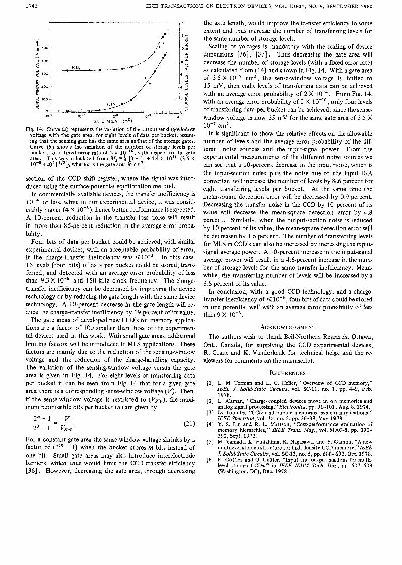
GATE AREA (cm‘)
Fig. 14. Curve (a) represents the variation of the output sensingwindow voltage with the gate area, for eight levels of data per bucket, assurn- ing that the sensing gate has the same area as that of the storage gates. Curve ( b ) shows the variation of the number of‘ !storage levels pe:r bucket, for a fixed error rate of 2 X lO-“ , with respect t o the gate area. This was calculated from M,= $ {3 + 1 +4.4 X lo1’ (3.5 X
+a)’ ] ‘ I 2 } , where a is the gate area in cm h . section of the CCD shift register, where the signal was intro- duced using the surface-potential equilibration method.
In commercially available devices, the transfer inefficiency is or less, while in our experimental device, it was consid-
erably higher (4 X hence better performance is expected. A 10-percent reduction in the transfer loss noise will result in more than 85-percent reduction in the average error proba- bility.
Four bits of data per bucket could be achieved, with similar experimental devices, with an acceptable probability of error, if the charge-transfer inefficiency was <IO’-” In this case, 16 levels (four bits) of data per bucket could be stored, trans- ferred, and detected with an average error probability of less than 9.3 X and 150-kHz clock frequency. The charge- transfer inefficiency can be decreased by improving the device technology or by reducing the gate length with the same device technology. A 10-percent decrease in the gate length will re- duce the charge-transfer inefficiency by 19 percent of itsvalue.
The gate areas of developed new CCD’s for memory applica- tions are a factor of 100 smaller than those of the experimen- tal devices used in this work. With small gate areas, additional limiting factors will be introduced in MLS applications. These factors are mainly due to the reduction of the sensingwindow voltage and the reduction of the charge-handling capacity. The variation of the sensing-window voltage versus the gate area is given in Fig. 14. For eight levels of transferring data per bucket it can be seen from Fig. 14 that for a given gate area there is a corresponding sense-window voltage ( V ) . Then, if the sense-window voltage is restricted to (Vsw), the maxi- mum permissible bits per bucket (n) are given by
For a constant gate area the sense-window voltage shrinks by a factor of ( 2 m - 1) when the bucket stores m bits instead of one bit. Small gate areas may also introduce interelectrode barriers, which thus would limit the CCD transfer efficiency
the gate length, would improve the transfer efficiency to some extent and thus increase the number of transferring levels for the same number of’storage levels.
Scaling of voltagcs is mandatory with the scaling of device dimensions [36], [37]. Thus decreasing the gate area will decrease the number of storage levels (with a fixed error rate) as calculated from (14) and shown in Fig. 14. With a gate area of 3.5 X 1 0-7 cm2 , the sense-window voltage is limited to 15 mV, then eight levels of transferring data can be achieved with an average error probability of 2 X From Fig. 14, with an average error probability of 2 X only four levels of transferring data per bucket can be achieved, since the sense- window voltage is ]now 35 mV for the same gate area of 3.5 X
It is significant to show the relative effects on the allowable number of levels and the average error probability of the dif- ferent noise sources and the input-signal power. From the experimental measurements of the different noise sources we can see that a 10-percent decrease in the input noise, which is the input-section noise plus the noise due to the input D/A converter, will increase the number of levels by 8.6 percent for eight transferring levels per bucket. At the same time the mean-square detection error will be decreased by 0.9 percent. Decreasing the transfer noise in the CCD by 10 percent of its value will decrease the mean-square detection error by 4.8 percent. Similarly, when the output-section noise is reduced by 10 percent of its value, the mean-square detection error will be decreased by I .6 percent. The number of transferring levels for MLS in CCD’s can also be increased by increasing the input- signal average power. A 10-percent increase in the input-signal average power will result in a 4.6-percent increase in the num- ber of storage levels for the same transfer inefficiency. Mean- while, the transferring number of levels will be increased by a 3.8 percent of its value.
In conclusion, with a good CCD technology, and a charge- transfer inefficiency of , four bits of data could be stored in one potential well with an average error probability of less than 9 X
cm2.
ACKNOWLEDGMENT The authors wish to thank Bell-Northern Research, Ottawa,
Ont., Canada, for supplying the CCD experimental devices, R. Grant and K. Vanderkruk for technical help, and the re- viewers for comments on the manuscript.
REFERENCES [ l ] L. M. Terman and L. G. Heller, “Overview of CCD memory,”
IEEE J. Solid-state Circuits, vol. SC-11, no. 1, pp. 4-9, Feb. 1976.
[2] L. Altman, “Charge-coupled devices move in on memories and analog signal processing,” Electronics, pp. 91-101, Aug. 8, 1974.
[3] D. Toombs, “CCD and bubble memories: system implications,” IEEE Spectrum, vol. 15, no. 5, pp. 36-39, May 1978.
[4] Y. S. Lin and R. L. Mattson, “Cost-performance evaluation of memory hierarchies,” IEEE Trans. Mag., vol. MAG-8, pp. 390- 392, Sept. 1972.
[5] M. Yamada, K. Fujishima, K . Nagasawa, and Y. Gamou, “A new multilevel storage structure for high density CCD memory,”IEEE J. Solid-State Circuits, vol. SC-13, no. 5, pp. 688-692, Oct. 1978.
[6] E. Gottler and 0. Griiter, “Input and output stations for multi- level storage CCDs,’’ in IEEE IEDM Tech. Dig., pp. 607-609
[36]. However, decreasing the gate area, through decreasing (Washington, DC), Dec. 1978.
ZOHDY et al.: MULTILEVEL STORAGE IN CCD’s 1743
[7] P. K. Chatterjee, A. F. Tasch, Jr., H. S. Fu, and T. C. Holloway, “Enhanced capacity CCD,” ZEEE Trans. Electron Devices, vol. ED-25, no. 12,pp. 1374-1382, Dec. 1978.
[8] J. S. T. Huang, “Charge handling capacity in charge coupled devices,” ZEEE Trans. Electron Devices, vol. ED-24, no. 10, pp.
[9] W. Penney and L. Lau, MOS Zntegrated Circuits. New York: Van Nostrand, 1972, p. 47.
[ 101 S. M. Sze, Physics of Semiconductor Devices. New York: Wiley, 1969, p. 492.
[ 111 C. H. SBquin and A. M. Mohsen, “Linearity of electrical charge injection into charge-coupled devices,” ZEEE J. Solid-State Cir- cuits, vol. SC-10, no. 2, pp. 81-91, Apr. 1975.
[ 121 H. Taub and D. L. Schilling, Principles of Communication Sys- tems. New York: McGraw-Hill, 1971.
[13] K. K. Thornber, “Operational limitations of charge transfer de- vices,’’ Bell Syst. Tech. J . , vol. 52, no. 9, pp. 1453-1473, Nov. 1973.
[14] T. M. Chen and A. Van Der Ziel, “Hanbury Brown-Twiss type circuit for measuring small noise signals,” Proc. ZEEE, vol. 53, p. 395, 1965.
[15] R. H. Brown and R. Q. Twiss, “Correlation between photons in two coherent beams of light,” Nature (London), vol. 177, pp. 27-29, Jan. 1956.
[16] D. D. Buss, W. H. Bailey, and W. L. Eversole, “Noise in bucket- brigade devices,” ZEEE Trans. Electron Devices, vol. ED-22, no.
[ 171 S. G. Chamberlain and D. H. Harper, “MTF simulation including transmittance effects and experimental results of charge-coupled imagers,” ZEEE Trans. Electron Devices, vol. ED-25, no. 2, pp. 145-153, Feb. 1978.
[ 181 M. F. Tompsett, “Using charge coupled devices for analog delay,” in Proc. CCD Appl. Conf. (San Diego, CA), pp. 147-150, Sept. 1973.
[ 191 S. G. Chamberlain and B. Y. Woo, “Transient analysis of electri- cal charge injection into charge-coupled devices,”Znt. J. Electron., vol. 40, no. 6,pp. 569-586,1976.
[20] R. D. Baertsch, W. E. Engeler, H. S. Goldberg, C. M. Puckette, and J. J. Tiemann, “The design and operation of practical charge transfer transversal filters,” ZEEE J. Solid-State Circuits, vol. SC-11, no. 1, pp. 65-73, Feb. 1976.
[21] R. A. Haken, “Supply charge isolation-A simple surface poten- tial equilibration charge injection technique for charge-coupled devices,” ZEEE J. Solid-State Circuits, vol. SC-11, no. 1, pp. 189- 196, Feb. 1976.
[22] R. W. Brown and S . G. Chamberlain, “Quantum efficiency of a
1234-1238, Oct. 1977.
11, pp. 977-981, NOV. 1975.
silicon gate charge coupled optical imaging array,” Phys. Status Solidi, (a), vol. 20, pp. 675-685, 1973.
[23] J . E. Carnes and W. F. Kosonocky, “Noise sources in charge- coupled devices,” RCA Rev., vol. 33, pp. 327-343, June 1972.
[24] S. P. Emmons and D. D. Buss, “The performance of charge- coupled devi.ces in signal processing at low signal levels,” in Proc. CCD Appl. Conf. (San Diego, CA), pp. 189-205, Sept. 1973.
[25] K. K. Thornber and M. F. Tompsett, “Spectral density of noise generated in charge transfer devices,” ZEEE Trans. Electron De- vices, vol. ED-20, no. 4, pp. 456, Apr. 1973.
[26] M. F. Tompsett, “The quantitative effects of interface states on the performance of charge-coupled devices,” ZEEE Trans. Elec- tron Devices, vol. ED-20, no. 1, pp. 45-55, Jan. 1973.
[27] D. B. Scott and S. G. Chamberlain, “Experimental confirmation of an analytical model for charge transfer in charge-coupled devices,” ZEEE J. Solid-State Circuits, vol. SC-12, no. 1, pp. 45- 50, Feb. 1977.
[ 281 J. E. Carnes, W. F. Kosonocky, and P. A. Levine, “Measurements
564, Dec. 1973. of noise in charge-coupled devices,” RCA Rev., vol. 34, pp. 553-
[29] R. W. Brodersen and S. P. Emmons, “Noise in buried channel charge-coupled devices,” ZEEE J. Solid-state Circuits, vol. SC-11, no. 1, pp. 147-155, Feb. 1976.
[30] A. M. Mohsen, M. F. Tompsett, and C. H. Shquin, “Noise mea- surements in chargecoupled devices,” ZEEE Trans. Electron Devices, vol. ED-22, no. 5, pp. 209-218, May 1975.
[31] C. W. Eichelberger and W. J. Butler, “An analog-to-digital conver- ter using charge-transfer technology,” in IEEE ZSSCC Dig. Tech. Papers, pp. 94-95, Feb. 1977.
[ 3 21 K. K. Thornber, “Error rates of digital signals in charge transfer devices,” BellSyst. Tech. J., vol. 52, no. 11, pp. 1795-1809, Dec. 1973.
[33] B. P. Lathi, Communication Systems. New York: Wiley, 1968, pp. 408.
[ 341 G. L. Schnable, H. J. Ewald, and E. S. Schlegel, “MOS integrated circuit reliability,” ZEEE Trans. Rel., vol. R-21, pp. 12-19, Feb. 1972.
[35] M. Horiuchi and H. Katto, “FCAT-A low-voltage high-speed alterable n-channel nonvolatile memory device,” ZEEE Trans. Electron Devices, vol. ED-26, no. 6, pp. 914-918, June 1979.
[36] P. K. Chatterjee, G. W. Taylor, and A. F. Tasch, Jr., “Charge- coupled device structures for VLSI memories,” ZEEE Trans. Electron Devices,vol. ED-26, no. 6, pp. 871-881, June 1979.
[37] R. H. Dennard et al., “Design of ion-implanted MOSFET’s with very small physical dimensions,” ZEEE J. Solid-state Circuits, V O ~ . SC-9, p. 256,1974.


![Performance and Stability Limitations of Admittance-Based ......electromechanical haptic interface dynamics, a coupled human impedance model [17], and the rendered virtual admittance](https://img.pdfslide.net/doc/110x75/60e2c1820229ae2f2a082f23/performance-and-stability-limitations-of-admittance-based-electromechanical.jpg)