Embed Size (px)
Citation preview
LM2682
www.ti.com SNVS044B –NOVEMBER 1999–REVISED MAY 2013
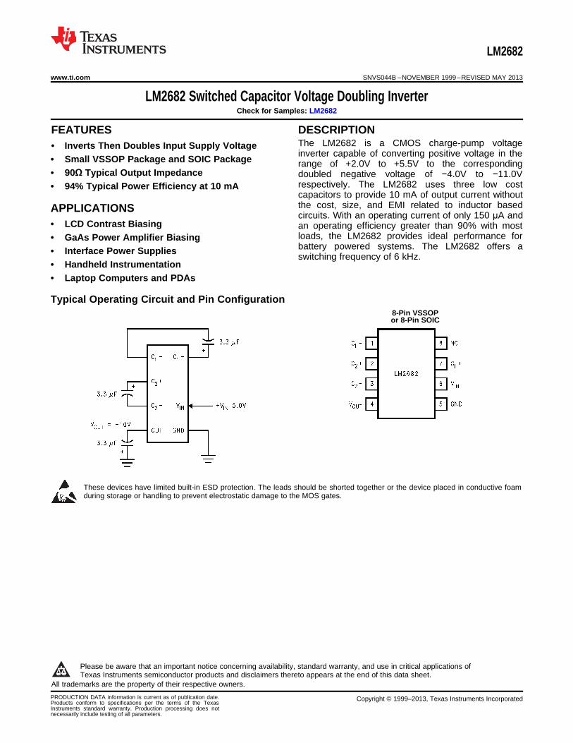
LM2682 Switched Capacitor Voltage Doubling InverterCheck for Samples: LM2682
1FEATURES DESCRIPTIONThe LM2682 is a CMOS charge-pump voltage
2• Inverts Then Doubles Input Supply Voltageinverter capable of converting positive voltage in the
• Small VSSOP Package and SOIC Package range of +2.0V to +5.5V to the corresponding• 90Ω Typical Output Impedance doubled negative voltage of −4.0V to −11.0V
respectively. The LM2682 uses three low cost• 94% Typical Power Efficiency at 10 mAcapacitors to provide 10 mA of output current withoutthe cost, size, and EMI related to inductor basedAPPLICATIONScircuits. With an operating current of only 150 μA and
• LCD Contrast Biasing an operating efficiency greater than 90% with mostloads, the LM2682 provides ideal performance for• GaAs Power Amplifier Biasingbattery powered systems. The LM2682 offers a• Interface Power Suppliesswitching frequency of 6 kHz.
• Handheld Instrumentation• Laptop Computers and PDAs
Typical Operating Circuit and Pin Configuration8-Pin VSSOPor 8-Pin SOIC
These devices have limited built-in ESD protection. The leads should be shorted together or the device placed in conductive foamduring storage or handling to prevent electrostatic damage to the MOS gates.
1
Please be aware that an important notice concerning availability, standard warranty, and use in critical applications ofTexas Instruments semiconductor products and disclaimers thereto appears at the end of this data sheet.
2All trademarks are the property of their respective owners.
PRODUCTION DATA information is current as of publication date. Copyright © 1999–2013, Texas Instruments IncorporatedProducts conform to specifications per the terms of the TexasInstruments standard warranty. Production processing does notnecessarily include testing of all parameters.
LM2682
SNVS044B –NOVEMBER 1999–REVISED MAY 2013 www.ti.com
Absolute Maximum Ratings (1)
Input Voltage (VIN) +5.8V
VIN dV/dT 1V/μsec
VOUT −11.6V
VOUT Short-Circuit Duration Continuous
Storage Temperature −65°C to +150°C
Lead Temperature Soldering +300°C
VSSOP 300 mWPower Dissipation (2)
SOIC 470 mW
TJMAX +150°C
(1) Absolute Maximum Ratings are those values beyond which damage to the device may occur. Operating Ratings indicate conditions forwhich the device is intended to be functional, but do not ensure specific performance limits. For ensured specifications and testconditions, see the Electrical Characteristics.
(2) The maximum power dissipation must be de-rated at elevated temperatures (only needed for TA>85°C) and is limited by TJMAX(maximum junction temperature), θJ-A (junction to ambient thermal resistance) and TA (ambient temperature). θJ-A is 140°C/W for theSOIC-8 package and 220°C/W for the VSSOP-8 package. The maximum power dissipation at any temperature is:PDissMAX = (TJMAX −TA)/θJ-A up to the value listed in the Absolute Maximum Ratings.
Operating RatingsHuman Body Model 2 kV
ESD Susceptibility (1)
Machine Model 200V
Ambient Temp. Range −40°C to +85°C
Junction Temp. Range −40°C to +125°C
(1) The human body model is a 100 pF capacitor discharged through a 1.5 kΩ resistor into each pin. The machine model is a 200pFcapacitor discharged directly into each pin.
LM2682Electrical CharacteristicsVIN = 5V and C1 = C2 = C3 = 3.3μF unless otherwise specified. Limits with bold typeface apply over the full operating ambienttemperature range, −40°C to +85°C, limits with standard typeface apply for TA = 25°C.
Symbol Parameter Conditions Min Typical (1) Max Units
VIN Supply Voltage Range RL = 2 kΩ 2.0 5.5 V
IIN Supply Current Open Circuit, No Load 150 300 μA400
ROUT VOUT Source Resistance IL = 10 mA 90 150 Ω200
IL=5 mA, VIN=2 V 110 250 ΩfOSC Oscillator Frequency See (2) 12 30 kHz
fSW Switching Frequency See (2) 6 15 kHz
ηPOWER Power Efficiency RL = 2k (3) 90 93 %
ηVOLTAGE Voltage Conversion Efficiency 99.9 %
(1) Typical numbers are at 25°C and represent the most likely norm.(2) The output switches operate at one half of the oscillator frequency, fOSC = 2fSW.(3) The minimum specification is specified by design and is not tested.
2 Submit Documentation Feedback Copyright © 1999–2013, Texas Instruments Incorporated
Product Folder Links: LM2682
LM2682
www.ti.com SNVS044B –NOVEMBER 1999–REVISED MAY 2013
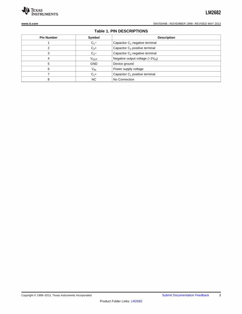
Table 1. PIN DESCRIPTIONS
Pin Number Symbol Description
1 C1− Capacitor C1 negative terminal
2 C2+ Capacitor C2 positive terminal
3 C2− Capacitor C2 negative terminal
4 VOUT Negative output voltage (−2VIN)
5 GND Device ground
6 VIN Power supply voltage
7 C1+ Capacitor C1 positive terminal
8 NC No Connection
Copyright © 1999–2013, Texas Instruments Incorporated Submit Documentation Feedback 3
Product Folder Links: LM2682
LM2682
SNVS044B –NOVEMBER 1999–REVISED MAY 2013 www.ti.com
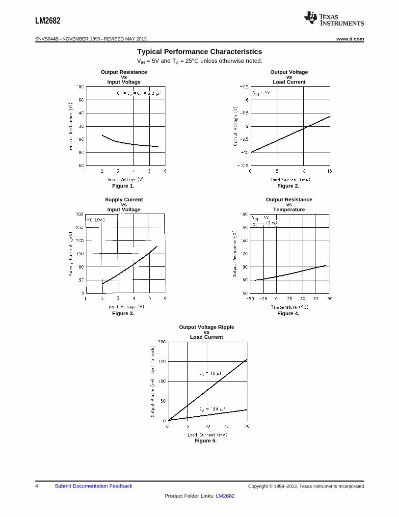
Typical Performance CharacteristicsVIN = 5V and TA = 25°C unless otherwise noted.
Output Resistance Output Voltagevs vs
Input Voltage Load Current
Figure 1. Figure 2.
Supply Current Output Resistancevs vs
Input Voltage Temperature
Figure 3. Figure 4.
Output Voltage Ripplevs
Load Current
Figure 5.
4 Submit Documentation Feedback Copyright © 1999–2013, Texas Instruments Incorporated
Product Folder Links: LM2682
LM2682
www.ti.com SNVS044B –NOVEMBER 1999–REVISED MAY 2013
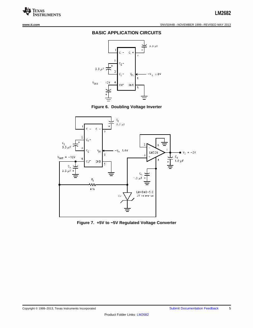
BASIC APPLICATION CIRCUITS
Figure 6. Doubling Voltage Inverter
Figure 7. +5V to −5V Regulated Voltage Converter
Copyright © 1999–2013, Texas Instruments Incorporated Submit Documentation Feedback 5
Product Folder Links: LM2682
LM2682
SNVS044B –NOVEMBER 1999–REVISED MAY 2013 www.ti.com
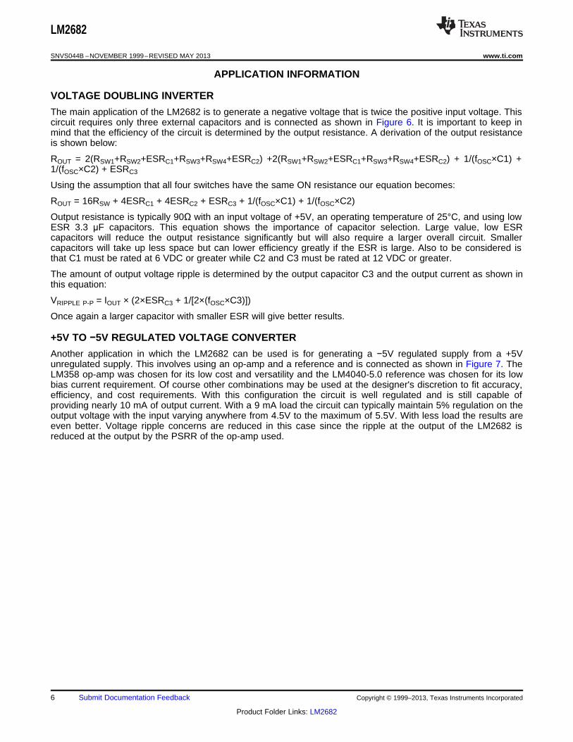
APPLICATION INFORMATION
VOLTAGE DOUBLING INVERTER
The main application of the LM2682 is to generate a negative voltage that is twice the positive input voltage. Thiscircuit requires only three external capacitors and is connected as shown in Figure 6. It is important to keep inmind that the efficiency of the circuit is determined by the output resistance. A derivation of the output resistanceis shown below:
ROUT = 2(RSW1+RSW2+ESRC1+RSW3+RSW4+ESRC2) +2(RSW1+RSW2+ESRC1+RSW3+RSW4+ESRC2) + 1/(fOSC×C1) +1/(fOSC×C2) + ESRC3
Using the assumption that all four switches have the same ON resistance our equation becomes:
ROUT = 16RSW + 4ESRC1 + 4ESRC2 + ESRC3 + 1/(fOSC×C1) + 1/(fOSC×C2)
Output resistance is typically 90Ω with an input voltage of +5V, an operating temperature of 25°C, and using lowESR 3.3 μF capacitors. This equation shows the importance of capacitor selection. Large value, low ESRcapacitors will reduce the output resistance significantly but will also require a larger overall circuit. Smallercapacitors will take up less space but can lower efficiency greatly if the ESR is large. Also to be considered isthat C1 must be rated at 6 VDC or greater while C2 and C3 must be rated at 12 VDC or greater.
The amount of output voltage ripple is determined by the output capacitor C3 and the output current as shown inthis equation:
VRIPPLE P-P = IOUT × (2×ESRC3 + 1/[2×(fOSC×C3)])
Once again a larger capacitor with smaller ESR will give better results.
+5V TO −5V REGULATED VOLTAGE CONVERTER
Another application in which the LM2682 can be used is for generating a −5V regulated supply from a +5Vunregulated supply. This involves using an op-amp and a reference and is connected as shown in Figure 7. TheLM358 op-amp was chosen for its low cost and versatility and the LM4040-5.0 reference was chosen for its lowbias current requirement. Of course other combinations may be used at the designer's discretion to fit accuracy,efficiency, and cost requirements. With this configuration the circuit is well regulated and is still capable ofproviding nearly 10 mA of output current. With a 9 mA load the circuit can typically maintain 5% regulation on theoutput voltage with the input varying anywhere from 4.5V to the maximum of 5.5V. With less load the results areeven better. Voltage ripple concerns are reduced in this case since the ripple at the output of the LM2682 isreduced at the output by the PSRR of the op-amp used.
6 Submit Documentation Feedback Copyright © 1999–2013, Texas Instruments Incorporated
Product Folder Links: LM2682
LM2682
www.ti.com SNVS044B –NOVEMBER 1999–REVISED MAY 2013
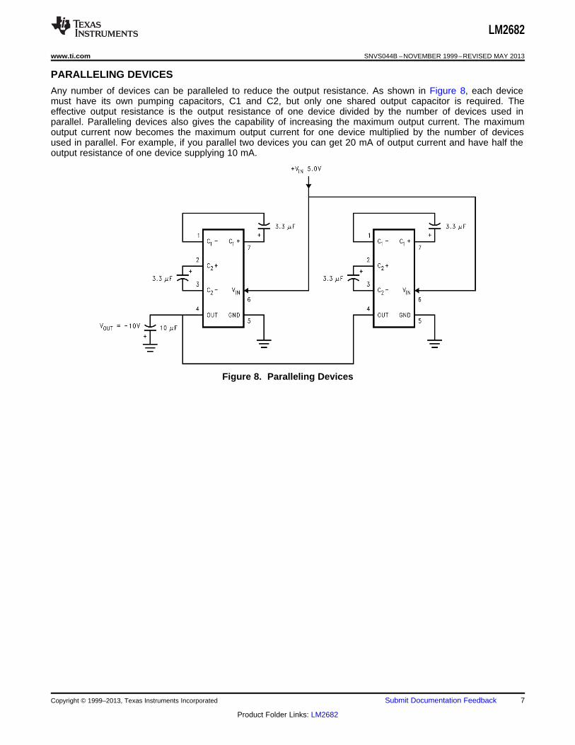
PARALLELING DEVICES
Any number of devices can be paralleled to reduce the output resistance. As shown in Figure 8, each devicemust have its own pumping capacitors, C1 and C2, but only one shared output capacitor is required. Theeffective output resistance is the output resistance of one device divided by the number of devices used inparallel. Paralleling devices also gives the capability of increasing the maximum output current. The maximumoutput current now becomes the maximum output current for one device multiplied by the number of devicesused in parallel. For example, if you parallel two devices you can get 20 mA of output current and have half theoutput resistance of one device supplying 10 mA.
Figure 8. Paralleling Devices
Copyright © 1999–2013, Texas Instruments Incorporated Submit Documentation Feedback 7
Product Folder Links: LM2682
LM2682
SNVS044B –NOVEMBER 1999–REVISED MAY 2013 www.ti.com
REVISION HISTORY
Changes from Revision A (May 2013) to Revision B Page
• Changed layout of National Data Sheet to TI format ............................................................................................................ 7
8 Submit Documentation Feedback Copyright © 1999–2013, Texas Instruments Incorporated
Product Folder Links: LM2682
PACKAGE OPTION ADDENDUM
www.ti.com 21-Oct-2014
Addendum-Page 1
PACKAGING INFORMATION
Orderable Device Status(1)
Package Type PackageDrawing
Pins PackageQty
Eco Plan(2)
Lead/Ball Finish(6)
MSL Peak Temp(3)
Op Temp (°C) Device Marking(4/5)
Samples
LM2682MM/NOPB ACTIVE VSSOP DGK 8 1000 Green (RoHS& no Sb/Br)
CU SN Level-1-260C-UNLIM -40 to 85 S11A
LM2682MMX/NOPB ACTIVE VSSOP DGK 8 3500 Green (RoHS& no Sb/Br)
CU SN Level-1-260C-UNLIM -40 to 85 S11A
(1) The marketing status values are defined as follows:ACTIVE: Product device recommended for new designs.LIFEBUY: TI has announced that the device will be discontinued, and a lifetime-buy period is in effect.NRND: Not recommended for new designs. Device is in production to support existing customers, but TI does not recommend using this part in a new design.PREVIEW: Device has been announced but is not in production. Samples may or may not be available.OBSOLETE: TI has discontinued the production of the device.
(2) Eco Plan - The planned eco-friendly classification: Pb-Free (RoHS), Pb-Free (RoHS Exempt), or Green (RoHS & no Sb/Br) - please check http://www.ti.com/productcontent for the latest availabilityinformation and additional product content details.TBD: The Pb-Free/Green conversion plan has not been defined.Pb-Free (RoHS): TI's terms "Lead-Free" or "Pb-Free" mean semiconductor products that are compatible with the current RoHS requirements for all 6 substances, including the requirement thatlead not exceed 0.1% by weight in homogeneous materials. Where designed to be soldered at high temperatures, TI Pb-Free products are suitable for use in specified lead-free processes.Pb-Free (RoHS Exempt): This component has a RoHS exemption for either 1) lead-based flip-chip solder bumps used between the die and package, or 2) lead-based die adhesive used betweenthe die and leadframe. The component is otherwise considered Pb-Free (RoHS compatible) as defined above.Green (RoHS & no Sb/Br): TI defines "Green" to mean Pb-Free (RoHS compatible), and free of Bromine (Br) and Antimony (Sb) based flame retardants (Br or Sb do not exceed 0.1% by weightin homogeneous material)
(3) MSL, Peak Temp. - The Moisture Sensitivity Level rating according to the JEDEC industry standard classifications, and peak solder temperature.
(4) There may be additional marking, which relates to the logo, the lot trace code information, or the environmental category on the device.
(5) Multiple Device Markings will be inside parentheses. Only one Device Marking contained in parentheses and separated by a "~" will appear on a device. If a line is indented then it is a continuationof the previous line and the two combined represent the entire Device Marking for that device.
(6) Lead/Ball Finish - Orderable Devices may have multiple material finish options. Finish options are separated by a vertical ruled line. Lead/Ball Finish values may wrap to two lines if the finishvalue exceeds the maximum column width.
Important Information and Disclaimer:The information provided on this page represents TI's knowledge and belief as of the date that it is provided. TI bases its knowledge and belief on informationprovided by third parties, and makes no representation or warranty as to the accuracy of such information. Efforts are underway to better integrate information from third parties. TI has taken andcontinues to take reasonable steps to provide representative and accurate information but may not have conducted destructive testing or chemical analysis on incoming materials and chemicals.TI and TI suppliers consider certain information to be proprietary, and thus CAS numbers and other limited information may not be available for release.
PACKAGE OPTION ADDENDUM
www.ti.com 21-Oct-2014
Addendum-Page 2
In no event shall TI's liability arising out of such information exceed the total purchase price of the TI part(s) at issue in this document sold by TI to Customer on an annual basis.
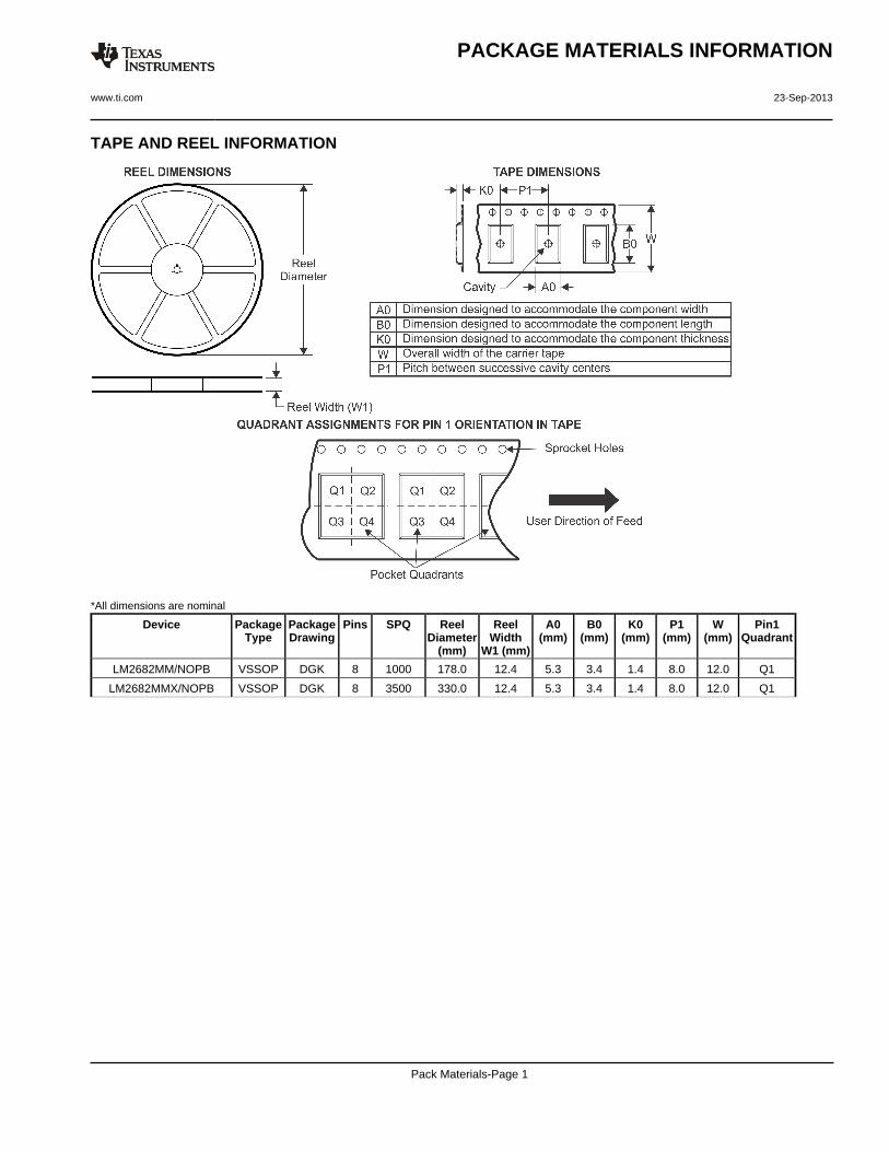
TAPE AND REEL INFORMATION
*All dimensions are nominal
Device PackageType
PackageDrawing
Pins SPQ ReelDiameter
(mm)
ReelWidth
W1 (mm)
A0(mm)
B0(mm)
K0(mm)
P1(mm)
W(mm)
Pin1Quadrant
LM2682MM/NOPB VSSOP DGK 8 1000 178.0 12.4 5.3 3.4 1.4 8.0 12.0 Q1
LM2682MMX/NOPB VSSOP DGK 8 3500 330.0 12.4 5.3 3.4 1.4 8.0 12.0 Q1
PACKAGE MATERIALS INFORMATION
www.ti.com 23-Sep-2013
Pack Materials-Page 1
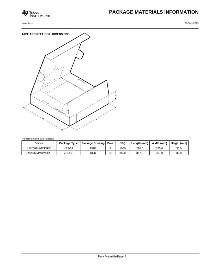
*All dimensions are nominal
Device Package Type Package Drawing Pins SPQ Length (mm) Width (mm) Height (mm)
LM2682MM/NOPB VSSOP DGK 8 1000 210.0 185.0 35.0
LM2682MMX/NOPB VSSOP DGK 8 3500 367.0 367.0 35.0
PACKAGE MATERIALS INFORMATION
www.ti.com 23-Sep-2013
Pack Materials-Page 2
IMPORTANT NOTICE
Texas Instruments Incorporated and its subsidiaries (TI) reserve the right to make corrections, enhancements, improvements and otherchanges to its semiconductor products and services per JESD46, latest issue, and to discontinue any product or service per JESD48, latestissue. Buyers should obtain the latest relevant information before placing orders and should verify that such information is current andcomplete. All semiconductor products (also referred to herein as “components”) are sold subject to TI’s terms and conditions of salesupplied at the time of order acknowledgment.TI warrants performance of its components to the specifications applicable at the time of sale, in accordance with the warranty in TI’s termsand conditions of sale of semiconductor products. Testing and other quality control techniques are used to the extent TI deems necessaryto support this warranty. Except where mandated by applicable law, testing of all parameters of each component is not necessarilyperformed.TI assumes no liability for applications assistance or the design of Buyers’ products. Buyers are responsible for their products andapplications using TI components. To minimize the risks associated with Buyers’ products and applications, Buyers should provideadequate design and operating safeguards.TI does not warrant or represent that any license, either express or implied, is granted under any patent right, copyright, mask work right, orother intellectual property right relating to any combination, machine, or process in which TI components or services are used. Informationpublished by TI regarding third-party products or services does not constitute a license to use such products or services or a warranty orendorsement thereof. Use of such information may require a license from a third party under the patents or other intellectual property of thethird party, or a license from TI under the patents or other intellectual property of TI.Reproduction of significant portions of TI information in TI data books or data sheets is permissible only if reproduction is without alterationand is accompanied by all associated warranties, conditions, limitations, and notices. TI is not responsible or liable for such altereddocumentation. Information of third parties may be subject to additional restrictions.Resale of TI components or services with statements different from or beyond the parameters stated by TI for that component or servicevoids all express and any implied warranties for the associated TI component or service and is an unfair and deceptive business practice.TI is not responsible or liable for any such statements.Buyer acknowledges and agrees that it is solely responsible for compliance with all legal, regulatory and safety-related requirementsconcerning its products, and any use of TI components in its applications, notwithstanding any applications-related information or supportthat may be provided by TI. Buyer represents and agrees that it has all the necessary expertise to create and implement safeguards whichanticipate dangerous consequences of failures, monitor failures and their consequences, lessen the likelihood of failures that might causeharm and take appropriate remedial actions. Buyer will fully indemnify TI and its representatives against any damages arising out of the useof any TI components in safety-critical applications.In some cases, TI components may be promoted specifically to facilitate safety-related applications. With such components, TI’s goal is tohelp enable customers to design and create their own end-product solutions that meet applicable functional safety standards andrequirements. Nonetheless, such components are subject to these terms.No TI components are authorized for use in FDA Class III (or similar life-critical medical equipment) unless authorized officers of the partieshave executed a special agreement specifically governing such use.Only those TI components which TI has specifically designated as military grade or “enhanced plastic” are designed and intended for use inmilitary/aerospace applications or environments. Buyer acknowledges and agrees that any military or aerospace use of TI componentswhich have not been so designated is solely at the Buyer's risk, and that Buyer is solely responsible for compliance with all legal andregulatory requirements in connection with such use.TI has specifically designated certain components as meeting ISO/TS16949 requirements, mainly for automotive use. In any case of use ofnon-designated products, TI will not be responsible for any failure to meet ISO/TS16949.
Products ApplicationsAudio www.ti.com/audio Automotive and Transportation www.ti.com/automotiveAmplifiers amplifier.ti.com Communications and Telecom www.ti.com/communicationsData Converters dataconverter.ti.com Computers and Peripherals www.ti.com/computersDLP® Products www.dlp.com Consumer Electronics www.ti.com/consumer-appsDSP dsp.ti.com Energy and Lighting www.ti.com/energyClocks and Timers www.ti.com/clocks Industrial www.ti.com/industrialInterface interface.ti.com Medical www.ti.com/medicalLogic logic.ti.com Security www.ti.com/securityPower Mgmt power.ti.com Space, Avionics and Defense www.ti.com/space-avionics-defenseMicrocontrollers microcontroller.ti.com Video and Imaging www.ti.com/videoRFID www.ti-rfid.comOMAP Applications Processors www.ti.com/omap TI E2E Community e2e.ti.comWireless Connectivity www.ti.com/wirelessconnectivity
Mailing Address: Texas Instruments, Post Office Box 655303, Dallas, Texas 75265Copyright © 2016, Texas Instruments Incorporated