Embed Size (px)
Citation preview
C1 = 0.1 µF
VI
470 W
R1
R2
C2 = 1 µF
VO
Adjustment
OutputInput
LM317L
Product
Folder
Sample &Buy
Technical
Documents
Tools &
Software
Support &Community
LM317LSLCS144E –JULY 2004–REVISED OCTOBER 2014
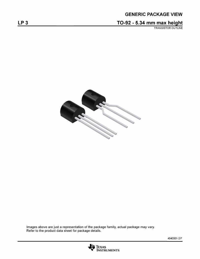
LM317L 3-Terminal Adjustable Regulator1 Features 3 Description
The LM317L device is an adjustable, 3-terminal,1• Output Voltage Range Adjustable 1.25 V to 32 V
positive-voltage regulator capable of supplyingWhen Used With External Resistor Divider100 mA over an output-voltage range of 1.25 V to
• Output Current Capability of 100 mA 32 V. It is exceptionally easy to use and requires only• Input Regulation Typically 0.01% Per Input- two external resistors to set the output voltage.
Voltage ChangeDevice Information• Output Regulation Typically 0.5%
PART NUMBER PACKAGE BODY SIZE (NOM)• Ripple Rejection Typically 80 dBSOIC (8) 4.90 mm × 3.91 mm• For Higher Output Current Requirements,TO-92 (3) 4.30 mm × 4.30 mmSee LM317M (500 mA) and LM317 (1.5 A) LM317LSOT-89 (3) 4.50 mm × 2.50 mmTSSOP (8) 3.00 mm × 4.40 mm2 Applications
• Electronic Points of Sale• Medical, Health, and Fitness Applications• Printers• Appliances and White Goods• TV Set-Top Boxes
4 Simplified Schematic
1
An IMPORTANT NOTICE at the end of this data sheet addresses availability, warranty, changes, use in safety-critical applications,intellectual property matters and other important disclaimers. PRODUCTION DATA.
LM317LSLCS144E –JULY 2004–REVISED OCTOBER 2014 www.ti.com
Table of Contents8.3 Feature Description................................................... 71 Features .................................................................. 18.4 Device Functional Modes.......................................... 72 Applications ........................................................... 1
9 Application and Implementation .......................... 83 Description ............................................................. 19.1 Application Information.............................................. 84 Simplified Schematic............................................. 19.2 Typical Application ................................................... 85 Revision History..................................................... 29.3 General Configurations ........................................... 106 Pin Configuration and Functions ......................... 3
10 Power Supply Recommendations ..................... 147 Specifications......................................................... 411 Layout................................................................... 147.1 Absolute Maximum Ratings ..................................... 4
11.1 Layout Guidelines ................................................. 147.2 Handling Ratings....................................................... 411.2 Layout Example .................................................... 147.3 Recommended Operating Conditions....................... 4
12 Device and Documentation Support ................. 157.4 Thermal Information .................................................. 412.1 Trademarks ........................................................... 157.5 Electrical Characteristics........................................... 512.2 Electrostatic Discharge Caution............................ 157.6 Typical Characteristics .............................................. 512.3 Glossary ................................................................ 158 Detailed Description .............................................. 6
13 Mechanical, Packaging, and Orderable8.1 Overview ................................................................... 6Information ........................................................... 158.2 Functional Block Diagram ......................................... 6
5 Revision History
Changes from Revision D (October 2011) to Revision E Page
• Added Device Information table, Pin Functions table, Handling Ratings table, Thermal Information table, TypicalCharacteristics, Detailed Description, Application and Implementation, Power Supply Recommendations, Layout,Device and Documentation Support, and Mechanical, Packaging, and Orderable Information sections .............................. 1
• Deleted Ordering Information table. ....................................................................................................................................... 1
2 Submit Documentation Feedback Copyright © 2004–2014, Texas Instruments Incorporated
Product Folder Links: LM317L
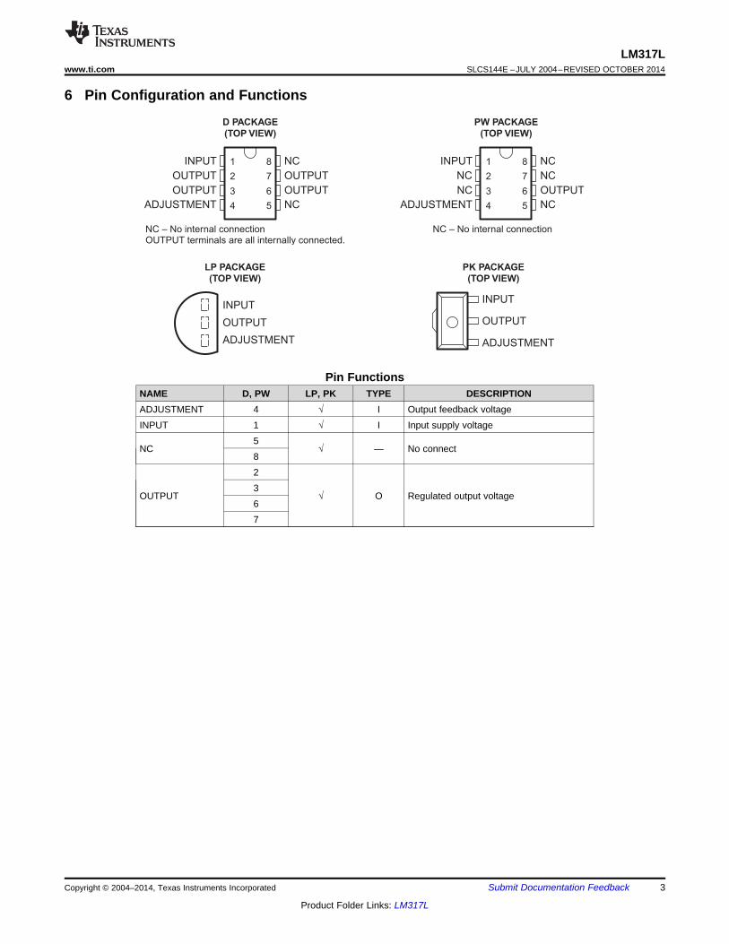
INPUT
OUTPUT
ADJUSTMENT
LP PACKAGE
(TOP VIEW)
INPUT
OUTPUT
ADJUSTMENT
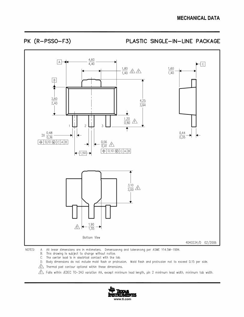
PK PACKAGE
(TOP VIEW)
1
2
3
4
8
7
6
5
INPUT
OUTPUT
OUTPUT
ADJUSTMENT
NC
OUTPUT
OUTPUT
NC
D PACKAGE
(TOP VIEW)
NC – No internal connectionOUTPUT terminals are all internally connected.
1
2
3
4
8
7
6
5
INPUT
NC
NC
ADJUSTMENT
NC
NC
OUTPUT
NC
PW PACKAGE
(TOP VIEW)
NC – No internal connection
LM317Lwww.ti.com SLCS144E –JULY 2004–REVISED OCTOBER 2014
6 Pin Configuration and Functions
Pin FunctionsNAME D, PW LP, PK TYPE DESCRIPTIONADJUSTMENT 4 √ I Output feedback voltageINPUT 1 √ I Input supply voltage
5NC √ — No connect
823
OUTPUT √ O Regulated output voltage67
Copyright © 2004–2014, Texas Instruments Incorporated Submit Documentation Feedback 3
Product Folder Links: LM317L
LM317LSLCS144E –JULY 2004–REVISED OCTOBER 2014 www.ti.com
7 Specifications
7.1 Absolute Maximum Ratings (1)
over operating temperature range (unless otherwise noted)MIN MAX UNIT
Vl – VO Input-to-output differential voltage 35 VTJ Operating virtual-junction temperature 150 °C
(1) Stresses beyond those listed under Absolute Maximum Ratings may cause permanent damage to the device. These are stress ratingsonly, and functional operation of the device at these or any other conditions beyond those indicated under Recommended OperatingConditions is not implied. Exposure to absolute-maximum-rated conditions for extended periods may affect device reliability.
7.2 Handling RatingsMIN MAX UNIT
Tstg Storage temperature range –65 150 °CHuman body model (HBM), per ANSI/ESDA/JEDEC JS-001, all 0 3000pins (1)
V(ESD) Electrostatic discharge VCharged device model (CDM), per JEDEC specification 0 2000JESD22-C101, all pins (2)
(1) JEDEC document JEP155 states that 500-V HBM allows safe manufacturing with a standard ESD control process.(2) JEDEC document JEP157 states that 250-V CDM allows safe manufacturing with a standard ESD control process.
7.3 Recommended Operating ConditionsMIN MAX UNIT
VO Output voltage 1.25 32 VVI – VO Input-to-output voltage differential 2.5 32 VIO Output current 2.5 100 mA
LM317LC 0 125TJ Operating virtual-junction temperature °C
LM317LI –40 125
7.4 Thermal InformationLM317L
THERMAL METRIC (1) UNITD LP PK PW8 PINS 3 PINS 3 PINS 8 PINS
RθJA Junction-to-ambient thermal resistance 97.1 139.5 51.5 149.4 °C/W
(1) For more information about traditional and new thermal metrics, see the IC Package Thermal Metrics application report (SPRA953).
4 Submit Documentation Feedback Copyright © 2004–2014, Texas Instruments Incorporated
Product Folder Links: LM317L
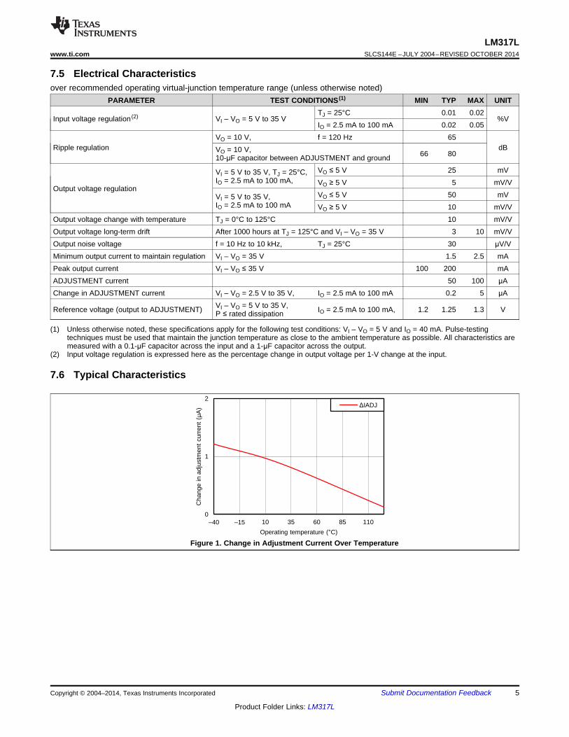
0
1
2
±40 ±15 10 35 60 85 110
Cha
nge
in a
djus
tmen
t cu
rren
t (
A)
Operating temperature (C)
ûIADJ
C001
LM317Lwww.ti.com SLCS144E –JULY 2004–REVISED OCTOBER 2014
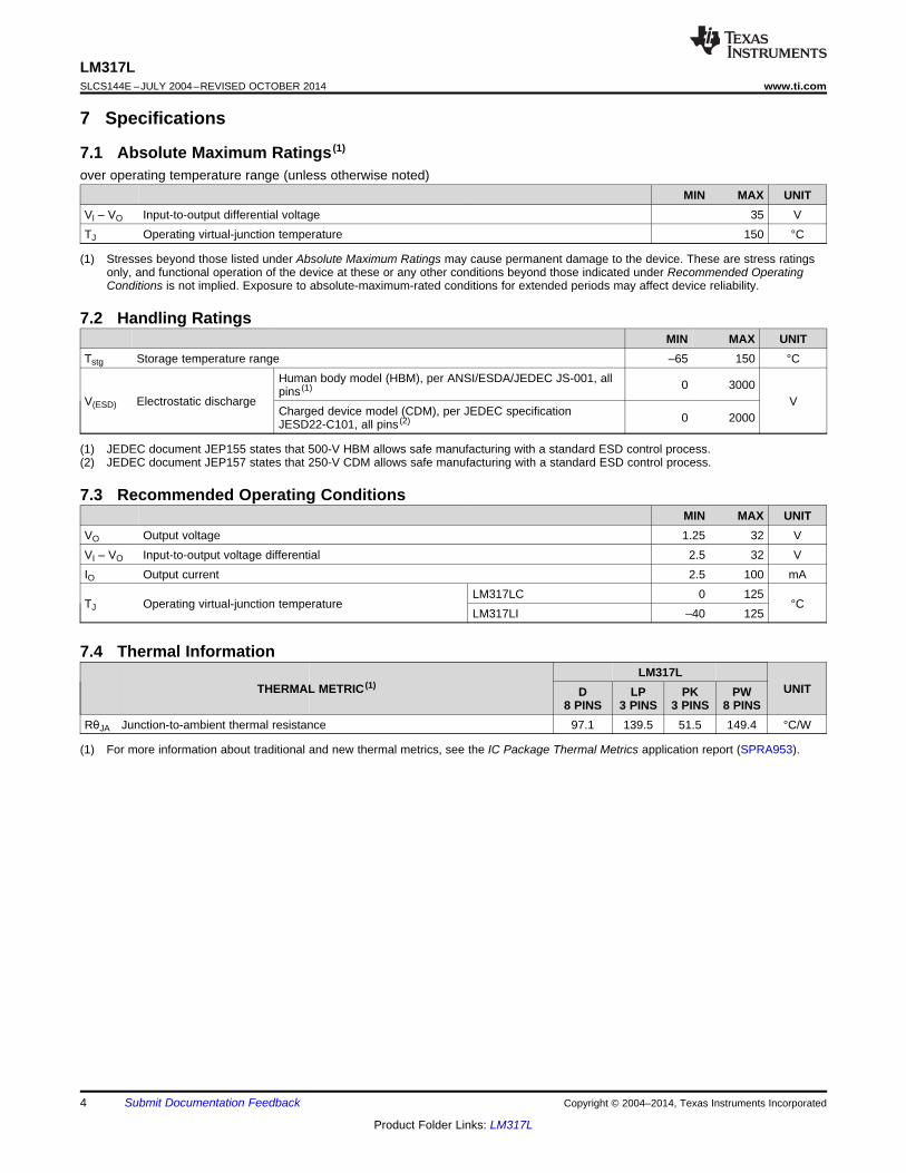
7.5 Electrical Characteristicsover recommended operating virtual-junction temperature range (unless otherwise noted)
PARAMETER TEST CONDITIONS (1) MIN TYP MAX UNITTJ = 25°C 0.01 0.02
Input voltage regulation (2) VI – VO = 5 V to 35 V %VIO = 2.5 mA to 100 mA 0.02 0.05
VO = 10 V, f = 120 Hz 65Ripple regulation dBVO = 10 V, 66 8010-μF capacitor between ADJUSTMENT and ground
VO ≤ 5 V 25 mVVI = 5 V to 35 V, TJ = 25°C,IO = 2.5 mA to 100 mA, VO ≥ 5 V 5 mV/V
Output voltage regulationVO ≤ 5 V 50 mVVI = 5 V to 35 V,
IO = 2.5 mA to 100 mA VO ≥ 5 V 10 mV/VOutput voltage change with temperature TJ = 0°C to 125°C 10 mV/VOutput voltage long-term drift After 1000 hours at TJ = 125°C and VI – VO = 35 V 3 10 mV/VOutput noise voltage f = 10 Hz to 10 kHz, TJ = 25°C 30 μV/VMinimum output current to maintain regulation VI – VO = 35 V 1.5 2.5 mAPeak output current VI – VO ≤ 35 V 100 200 mAADJUSTMENT current 50 100 μAChange in ADJUSTMENT current VI – VO = 2.5 V to 35 V, IO = 2.5 mA to 100 mA 0.2 5 μA
VI – VO = 5 V to 35 V,Reference voltage (output to ADJUSTMENT) IO = 2.5 mA to 100 mA, 1.2 1.25 1.3 VP ≤ rated dissipation
(1) Unless otherwise noted, these specifications apply for the following test conditions: VI – VO = 5 V and IO = 40 mA. Pulse-testingtechniques must be used that maintain the junction temperature as close to the ambient temperature as possible. All characteristics aremeasured with a 0.1-μF capacitor across the input and a 1-μF capacitor across the output.
(2) Input voltage regulation is expressed here as the percentage change in output voltage per 1-V change at the input.
7.6 Typical Characteristics
Figure 1. Change in Adjustment Current Over Temperature
Copyright © 2004–2014, Texas Instruments Incorporated Submit Documentation Feedback 5
Product Folder Links: LM317L
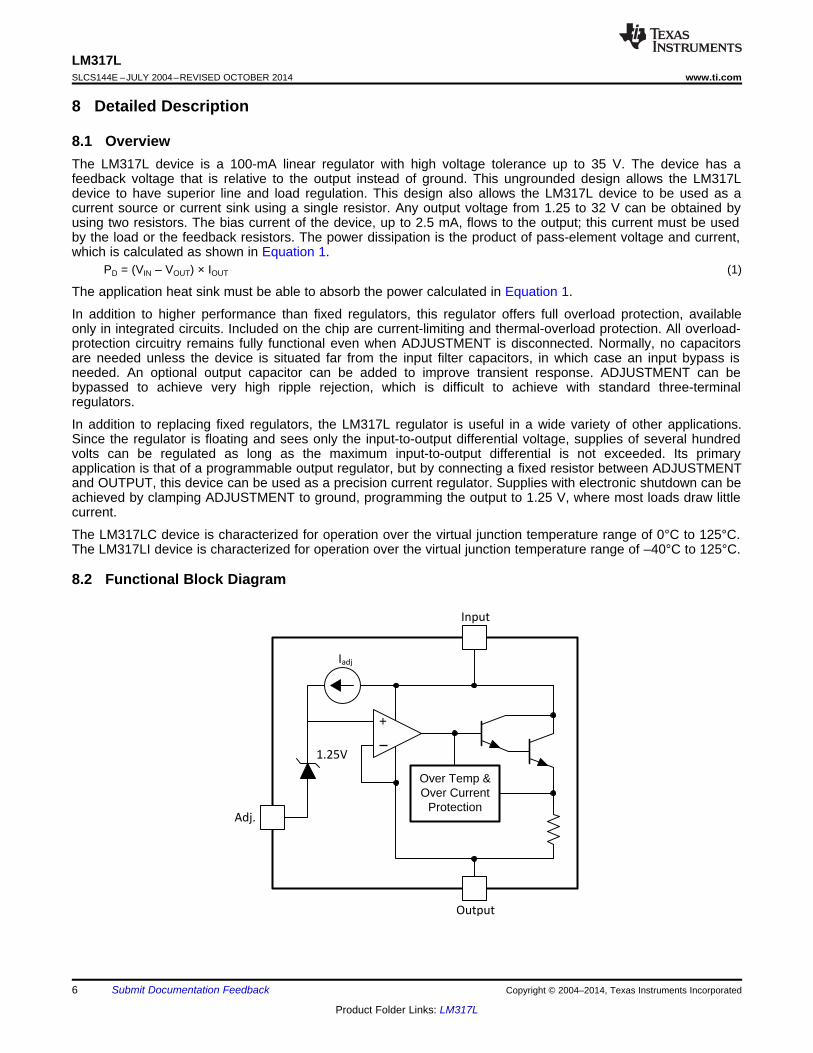
+
Over Temp & Over Current
Protection
Input
Adj.
Output
1.25V
Iadj
LM317LSLCS144E –JULY 2004–REVISED OCTOBER 2014 www.ti.com
8 Detailed Description
8.1 OverviewThe LM317L device is a 100-mA linear regulator with high voltage tolerance up to 35 V. The device has afeedback voltage that is relative to the output instead of ground. This ungrounded design allows the LM317Ldevice to have superior line and load regulation. This design also allows the LM317L device to be used as acurrent source or current sink using a single resistor. Any output voltage from 1.25 to 32 V can be obtained byusing two resistors. The bias current of the device, up to 2.5 mA, flows to the output; this current must be usedby the load or the feedback resistors. The power dissipation is the product of pass-element voltage and current,which is calculated as shown in Equation 1.
PD = (VIN – VOUT) × IOUT (1)
The application heat sink must be able to absorb the power calculated in Equation 1.
In addition to higher performance than fixed regulators, this regulator offers full overload protection, availableonly in integrated circuits. Included on the chip are current-limiting and thermal-overload protection. All overload-protection circuitry remains fully functional even when ADJUSTMENT is disconnected. Normally, no capacitorsare needed unless the device is situated far from the input filter capacitors, in which case an input bypass isneeded. An optional output capacitor can be added to improve transient response. ADJUSTMENT can bebypassed to achieve very high ripple rejection, which is difficult to achieve with standard three-terminalregulators.
In addition to replacing fixed regulators, the LM317L regulator is useful in a wide variety of other applications.Since the regulator is floating and sees only the input-to-output differential voltage, supplies of several hundredvolts can be regulated as long as the maximum input-to-output differential is not exceeded. Its primaryapplication is that of a programmable output regulator, but by connecting a fixed resistor between ADJUSTMENTand OUTPUT, this device can be used as a precision current regulator. Supplies with electronic shutdown can beachieved by clamping ADJUSTMENT to ground, programming the output to 1.25 V, where most loads draw littlecurrent.
The LM317LC device is characterized for operation over the virtual junction temperature range of 0°C to 125°C.The LM317LI device is characterized for operation over the virtual junction temperature range of –40°C to 125°C.
8.2 Functional Block Diagram
6 Submit Documentation Feedback Copyright © 2004–2014, Texas Instruments Incorporated
Product Folder Links: LM317L
LM317Lwww.ti.com SLCS144E –JULY 2004–REVISED OCTOBER 2014
8.3 Feature Description
8.3.1 NPN Darlington Output DriveNPN Darlington output topology provides naturally low output impedance and an output capacitor is optional. Tosupport maximum current and lowest temperature, 2.5-V headroom is recommended (VI – VO).
8.3.2 Overload BlockOver-current and over-temperature shutdown protects the device against overload or damage from operating inexcessive heat.
8.3.3 Programmable FeedbackOp amp with 1.25-V offset input at the ADJUST pin provides easy output voltage or current (not both)programming. For current regulation applications, a single resistor whose resistance value is 1.25 V / IOUT andpower rating is greater than (1.25 V)2 / R should be used. For voltage regulation applications, two resistors setthe output voltage. See Typical Application for a schematic and the resistor formula.
8.4 Device Functional Modes
8.4.1 Normal operationThe device OUTPUT pin will source current necessary to make OUTPUT pin 1.25 V greater than ADJUSTterminal to provide output regulation.
8.4.2 Operation With Low Input VoltageThe device requires up to 2.5-V headroom (VI – VO) to operate in regulation. With less headroom, the devicemay drop out and OUTPUT voltage will be INPUT voltage minus drop out voltage.
8.4.3 Operation at Light LoadsThe device passes its bias current to the OUTPUT pin. The load or feedback must consume this minimumcurrent for regulation or the output may be too high.
8.4.4 Operation In Self ProtectionWhen an overload occurs the device will shut down Darlington NPN output stage or reduce the output current toprevent device damage. The device will automatically reset from the overload. The output may be reduced oralternate between on and off until the overload is removed.
Copyright © 2004–2014, Texas Instruments Incorporated Submit Documentation Feedback 7
Product Folder Links: LM317L
C1 = 0.1 µF
VI
470 W
R1
R2
C2 = 1 µF
VO
Adjustment
OutputInput
LM317L
LM317LSLCS144E –JULY 2004–REVISED OCTOBER 2014 www.ti.com
9 Application and Implementation
NOTEInformation in the following applications sections is not part of the TI componentspecification, and TI does not warrant its accuracy or completeness. TI’s customers areresponsible for determining suitability of components for their purposes. Customers shouldvalidate and test their design implementation to confirm system functionality.
9.1 Application InformationThe two output resistors are the only components required to adjust VOUT.
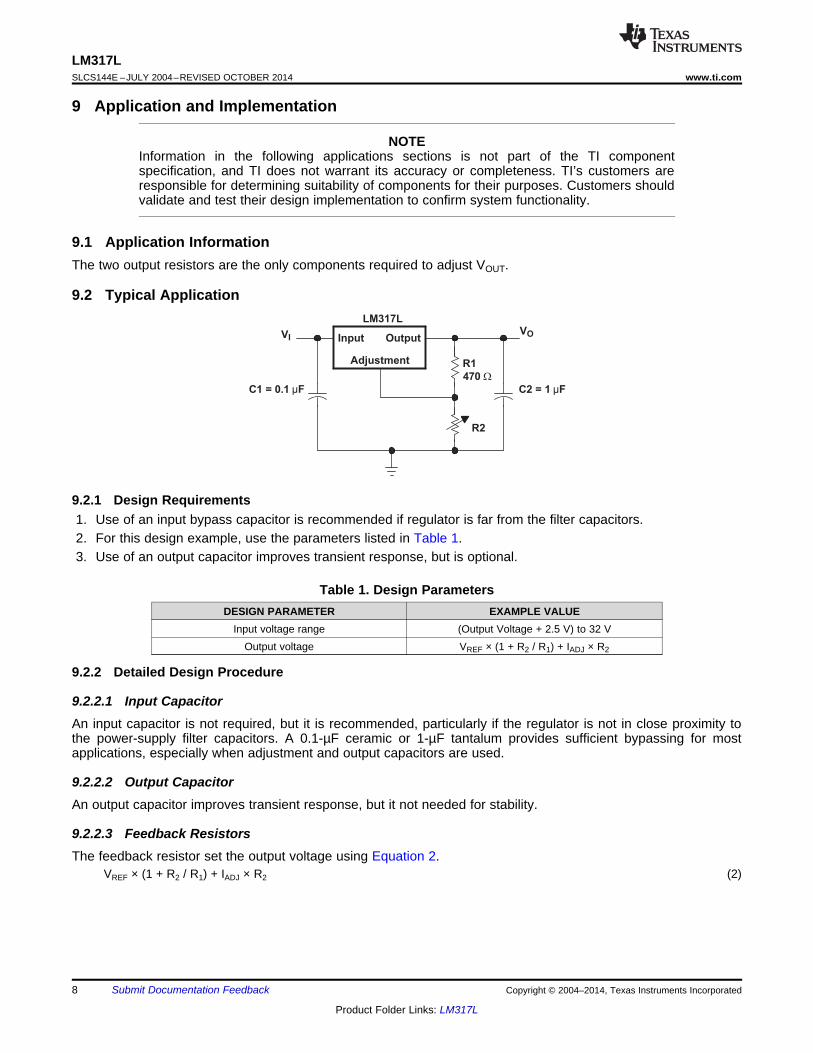
9.2 Typical Application
9.2.1 Design Requirements1. Use of an input bypass capacitor is recommended if regulator is far from the filter capacitors.2. For this design example, use the parameters listed in Table 1.3. Use of an output capacitor improves transient response, but is optional.
Table 1. Design ParametersDESIGN PARAMETER EXAMPLE VALUE
Input voltage range (Output Voltage + 2.5 V) to 32 VOutput voltage VREF × (1 + R2 / R1) + IADJ × R2
9.2.2 Detailed Design Procedure
9.2.2.1 Input CapacitorAn input capacitor is not required, but it is recommended, particularly if the regulator is not in close proximity tothe power-supply filter capacitors. A 0.1-µF ceramic or 1-µF tantalum provides sufficient bypassing for mostapplications, especially when adjustment and output capacitors are used.
9.2.2.2 Output CapacitorAn output capacitor improves transient response, but it not needed for stability.
9.2.2.3 Feedback ResistorsThe feedback resistor set the output voltage using Equation 2.
VREF × (1 + R2 / R1) + IADJ × R2 (2)
8 Submit Documentation Feedback Copyright © 2004–2014, Texas Instruments Incorporated
Product Folder Links: LM317L
VI VO (V)
VA
DJU
ST
ME
NT (
V)
0 6.25 12.5 18.75 25 31.25 37.5 42.51.2
1.22
1.24
1.26
1.28
1.3
D001
40qC0qC25qC125qC
2OUT REF ADJ 2
1
RV V 1 (I R )
R
æ ö= ´ + + ´ç ÷
è ø
LM317Lwww.ti.com SLCS144E –JULY 2004–REVISED OCTOBER 2014
9.2.2.4 Adjustment Terminal CapacitorThe optional adjustment pin capacitor will improve ripple rejection by preventing the amplification of the ripple.When capacitor is used and VOUT > 6 V, a protection diode from adjust to output is recommended.
9.2.2.5 Design Options and ParametersCommon Linear Regulator designs are concerned with the following parameters:• Input voltage range• Input capacitor range• Output voltage• Output current rating• Output capacitor range• Input short protection• Stability• Ripple rejection
9.2.2.6 Output VoltageVO is calculated as shown in Equation 3.
(3)
Because IADJ typically is 50 µA, it is negligible in most applications.
9.2.2.7 Ripple RejectionCADJ is used to improve ripple rejection; it prevents amplification of the ripple as the output voltage is adjustedhigher. If CADJ is used, it is best to include protection diodes.
9.2.2.8 Input Short ProtectionIf the input is shorted to ground during a fault condition, protection diodes provide measures to prevent thepossibility of external capacitors discharging through low-impedance paths in the IC. By providing low-impedancedischarge paths for CO and CADJ, respectively, D1 and D2 prevent the capacitors from discharging into the outputof the regulator.
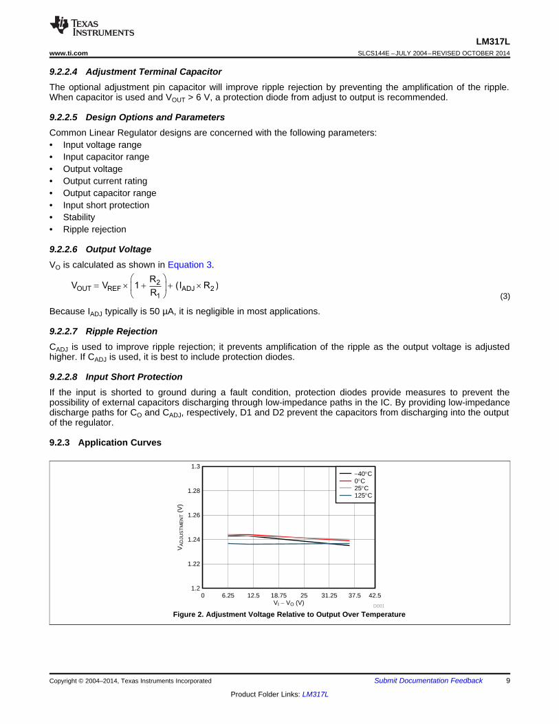
9.2.3 Application Curves
Figure 2. Adjustment Voltage Relative to Output Over Temperature
Copyright © 2004–2014, Texas Instruments Incorporated Submit Documentation Feedback 9
Product Folder Links: LM317L
VI
R1Adjustment
OutputInput
LM317L
Ilimit1.25R1
=
VO
R2 = 3 kW
1N4002
R3 =
820 W
−10 VC1 = 0.1 µF
35 V
Adjustment
OutputInput
LM317L
R1 = 120 W
2 3OUT REF
1
R RV V 1 10 V
R
æ ö+= + -ç ÷
è ø
R1 =
470 W
D1†
1N4002
C3 = 1 µFC2 = 10 µF
R2 =
10 kW
VI
+
+
−−
Adjustment
OutputInput
LM317L
VO
C1 =
0.1 µF
LM317LSLCS144E –JULY 2004–REVISED OCTOBER 2014 www.ti.com
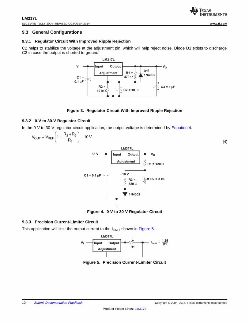
9.3 General Configurations
9.3.1 Regulator Circuit With Improved Ripple RejectionC2 helps to stabilize the voltage at the adjustment pin, which will help reject noise. Diode D1 exists to dischargeC2 in case the output is shorted to ground.
Figure 3. Regulator Circuit With Improved Ripple Rejection
9.3.2 0-V to 30-V Regulator CircuitIn the 0-V to 30-V regulator circuit application, the output voltage is determined by Equation 4.
(4)
Figure 4. 0-V to 30-V Regulator Circuit
9.3.3 Precision Current-Limiter CircuitThis application will limit the output current to the ILIMIT shown in Figure 5.
Figure 5. Precision Current-Limiter Circuit
10 Submit Documentation Feedback Copyright © 2004–2014, Texas Instruments Incorporated
Product Folder Links: LM317L
R1 =
470 Ω
R2 = 5.1 kΩ
C1 = 25 µF2N2905
R3 = 50 kΩ
1N4002
VO = 15 VVI
LM317L
Adjustment
OutputInput
R3 = 240 Ω
VI
C1 = 0.1 µF
C2 = 1 µF
Output
Adjust
VO
R2 = 1.5 kΩ
R1 = 470 Ω
LM317L
R4 = 2 kΩ
Adjustment
OutputInputLM317L
Adjustment
OutputInput
LM317Lwww.ti.com SLCS144E –JULY 2004–REVISED OCTOBER 2014
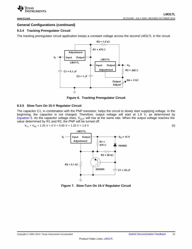
General Configurations (continued)9.3.4 Tracking Preregulator CircuitThe tracking preregulator circuit application keeps a constant voltage across the second LM317L in the circuit.
Figure 6. Tracking Preregulator Circuit
9.3.5 Slow-Turn On 15-V Regulator CircuitThe capacitor C1, in combination with the PNP transistor, helps the circuit to slowly start supplying voltage. In thebeginning, the capacitor is not charged. Therefore, output voltage will start at 1.9 V, as determined byEquation 5. As the capacitor voltage rises, VOUT will rise at the same rate. When the output voltage reaches thevalue determined by R1 and R2, the PNP will be turned off.
VC1 + VBE + 1.25 V = 0 V + 0.65 V + 1.25 V = 1.9 V (5)
Figure 7. Slow-Turn On 15-V Regulator Circuit
Copyright © 2004–2014, Texas Instruments Incorporated Submit Documentation Feedback 11
Product Folder Links: LM317L
1.1 kΩ
240 Ω
V−
VI
LM317L
Adjustment
OutputInput
ICHG
RVBE
ICHG
VBE =
VI
24 ΩLM317L
Adjustment
OutputInput
LM317LSLCS144E –JULY 2004–REVISED OCTOBER 2014 www.ti.com
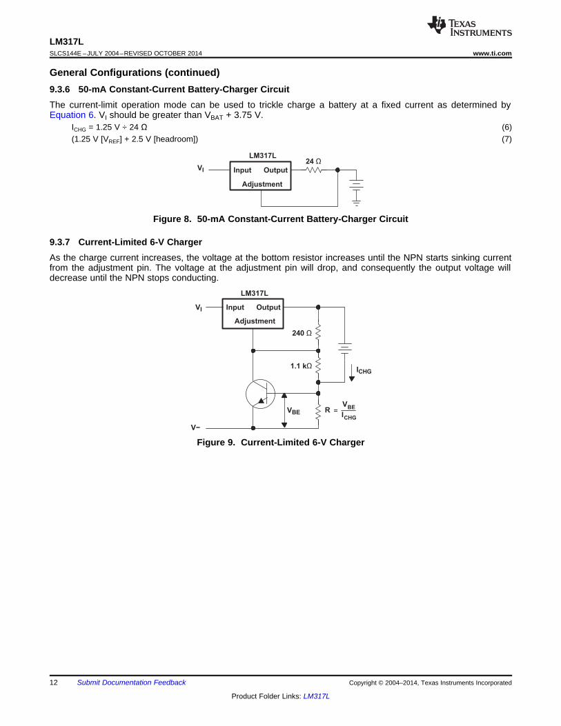
General Configurations (continued)9.3.6 50-mA Constant-Current Battery-Charger CircuitThe current-limit operation mode can be used to trickle charge a battery at a fixed current as determined byEquation 6. VI should be greater than VBAT + 3.75 V.
ICHG = 1.25 V ÷ 24 Ω (6)(1.25 V [VREF] + 2.5 V [headroom]) (7)
Figure 8. 50-mA Constant-Current Battery-Charger Circuit
9.3.7 Current-Limited 6-V ChargerAs the charge current increases, the voltage at the bottom resistor increases until the NPN starts sinking currentfrom the adjustment pin. The voltage at the adjustment pin will drop, and consequently the output voltage willdecrease until the NPN stops conducting.
Figure 9. Current-Limited 6-V Charger
12 Submit Documentation Feedback Copyright © 2004–2014, Texas Instruments Incorporated
Product Folder Links: LM317L
500 W
VO
47 µF
1N4002120 W
10 µF
10 µF
5 kW
22 W
5 kW
2N2905
TIP73
VI
RL
LM317L
Adjustment
OutputInput
LM317Lwww.ti.com SLCS144E –JULY 2004–REVISED OCTOBER 2014
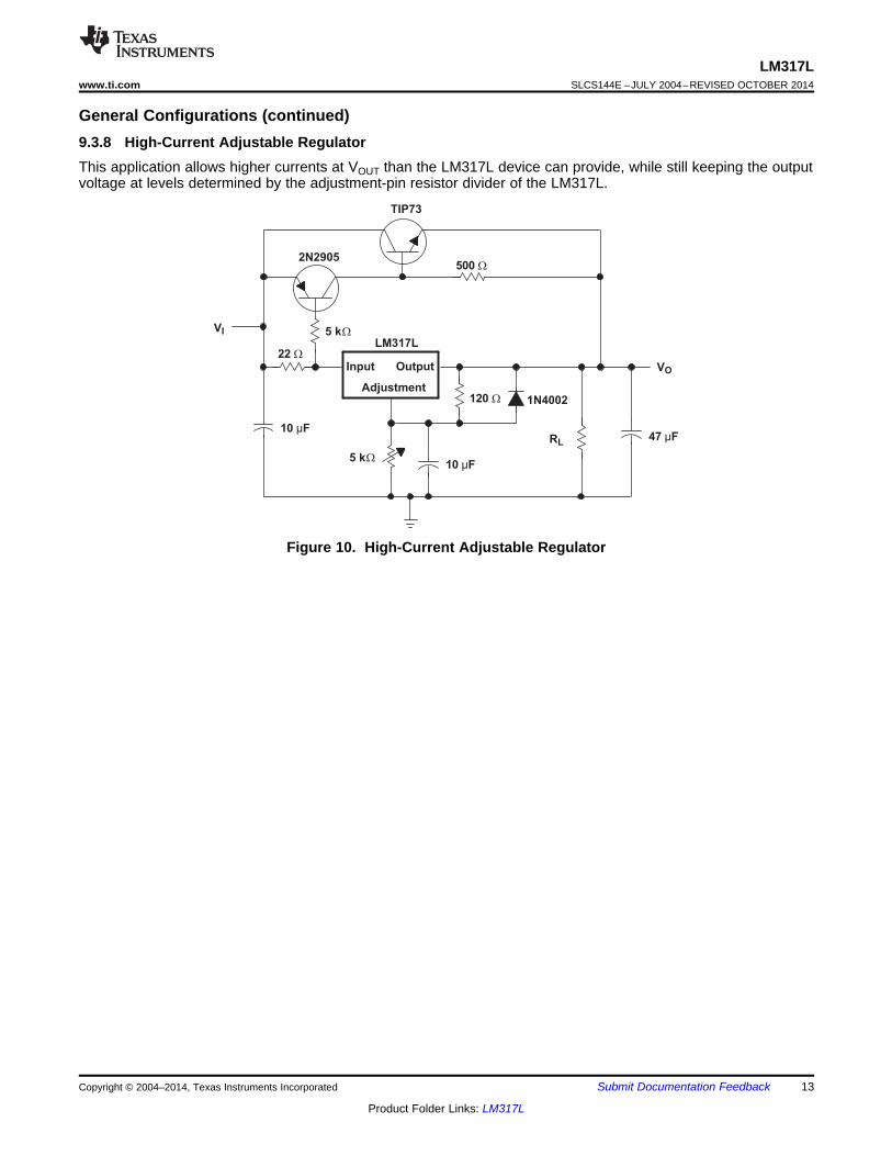
General Configurations (continued)9.3.8 High-Current Adjustable RegulatorThis application allows higher currents at VOUT than the LM317L device can provide, while still keeping the outputvoltage at levels determined by the adjustment-pin resistor divider of the LM317L.
Figure 10. High-Current Adjustable Regulator
Copyright © 2004–2014, Texas Instruments Incorporated Submit Documentation Feedback 13
Product Folder Links: LM317L
R1
OUTPUT
INP
UT
OU
TP
UT
AD
J/G
ND
R2
Cadj
COUT
0.1 Fμ 10 Fμ
Gro
und
Ground
High
Frequency
Bypass
Capacitor
High Input
Bypass
Capacitor
Power
LM317LSLCS144E –JULY 2004–REVISED OCTOBER 2014 www.ti.com
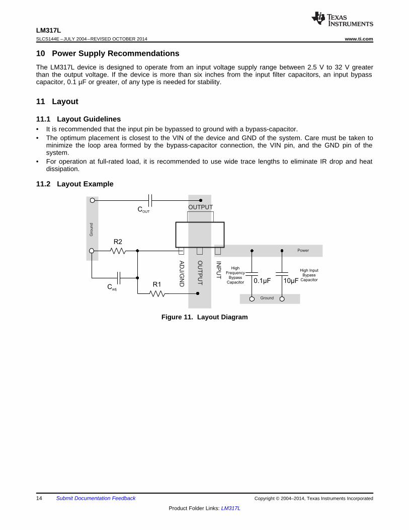
10 Power Supply RecommendationsThe LM317L device is designed to operate from an input voltage supply range between 2.5 V to 32 V greaterthan the output voltage. If the device is more than six inches from the input filter capacitors, an input bypasscapacitor, 0.1 µF or greater, of any type is needed for stability.
11 Layout
11.1 Layout Guidelines• It is recommended that the input pin be bypassed to ground with a bypass-capacitor.• The optimum placement is closest to the VIN of the device and GND of the system. Care must be taken to
minimize the loop area formed by the bypass-capacitor connection, the VIN pin, and the GND pin of thesystem.
• For operation at full-rated load, it is recommended to use wide trace lengths to eliminate IR drop and heatdissipation.
11.2 Layout Example
Figure 11. Layout Diagram
14 Submit Documentation Feedback Copyright © 2004–2014, Texas Instruments Incorporated
Product Folder Links: LM317L
LM317Lwww.ti.com SLCS144E –JULY 2004–REVISED OCTOBER 2014
12 Device and Documentation Support
12.1 TrademarksAll trademarks are the property of their respective owners.
12.2 Electrostatic Discharge CautionThese devices have limited built-in ESD protection. The leads should be shorted together or the device placed in conductive foamduring storage or handling to prevent electrostatic damage to the MOS gates.
12.3 GlossarySLYZ022 — TI Glossary.
This glossary lists and explains terms, acronyms, and definitions.
13 Mechanical, Packaging, and Orderable InformationThe following pages include mechanical, packaging, and orderable information. This information is the mostcurrent data available for the designated devices. This data is subject to change without notice and revision ofthis document. For browser-based versions of this data sheet, refer to the left-hand navigation.
Copyright © 2004–2014, Texas Instruments Incorporated Submit Documentation Feedback 15
Product Folder Links: LM317L
PACKAGE OPTION ADDENDUM
www.ti.com 25-Sep-2021
Addendum-Page 1
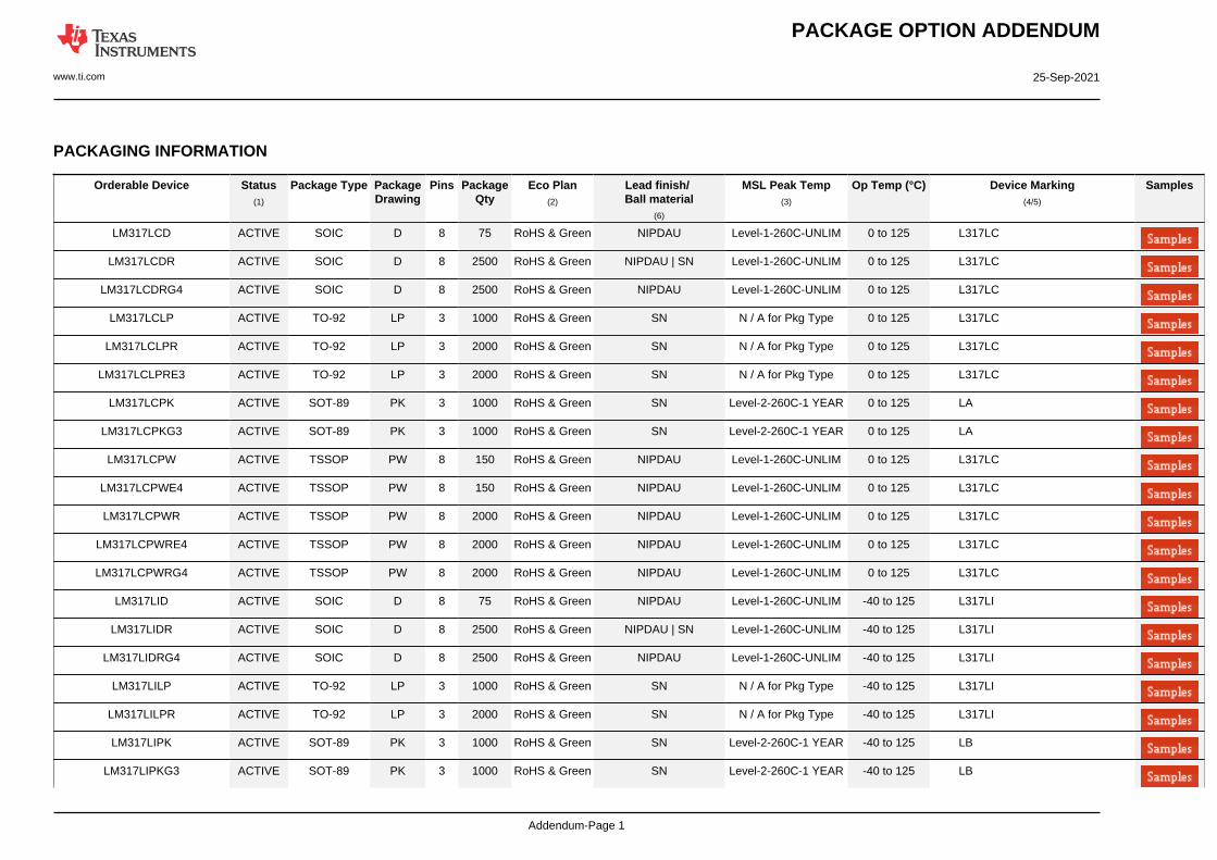
PACKAGING INFORMATION
Orderable Device Status(1)
Package Type PackageDrawing
Pins PackageQty
Eco Plan(2)
Lead finish/Ball material
(6)
MSL Peak Temp(3)
Op Temp (°C) Device Marking(4/5)
Samples
LM317LCD ACTIVE SOIC D 8 75 RoHS & Green NIPDAU Level-1-260C-UNLIM 0 to 125 L317LC
LM317LCDR ACTIVE SOIC D 8 2500 RoHS & Green NIPDAU | SN Level-1-260C-UNLIM 0 to 125 L317LC
LM317LCDRG4 ACTIVE SOIC D 8 2500 RoHS & Green NIPDAU Level-1-260C-UNLIM 0 to 125 L317LC
LM317LCLP ACTIVE TO-92 LP 3 1000 RoHS & Green SN N / A for Pkg Type 0 to 125 L317LC
LM317LCLPR ACTIVE TO-92 LP 3 2000 RoHS & Green SN N / A for Pkg Type 0 to 125 L317LC
LM317LCLPRE3 ACTIVE TO-92 LP 3 2000 RoHS & Green SN N / A for Pkg Type 0 to 125 L317LC
LM317LCPK ACTIVE SOT-89 PK 3 1000 RoHS & Green SN Level-2-260C-1 YEAR 0 to 125 LA
LM317LCPKG3 ACTIVE SOT-89 PK 3 1000 RoHS & Green SN Level-2-260C-1 YEAR 0 to 125 LA
LM317LCPW ACTIVE TSSOP PW 8 150 RoHS & Green NIPDAU Level-1-260C-UNLIM 0 to 125 L317LC
LM317LCPWE4 ACTIVE TSSOP PW 8 150 RoHS & Green NIPDAU Level-1-260C-UNLIM 0 to 125 L317LC
LM317LCPWR ACTIVE TSSOP PW 8 2000 RoHS & Green NIPDAU Level-1-260C-UNLIM 0 to 125 L317LC
LM317LCPWRE4 ACTIVE TSSOP PW 8 2000 RoHS & Green NIPDAU Level-1-260C-UNLIM 0 to 125 L317LC
LM317LCPWRG4 ACTIVE TSSOP PW 8 2000 RoHS & Green NIPDAU Level-1-260C-UNLIM 0 to 125 L317LC
LM317LID ACTIVE SOIC D 8 75 RoHS & Green NIPDAU Level-1-260C-UNLIM -40 to 125 L317LI
LM317LIDR ACTIVE SOIC D 8 2500 RoHS & Green NIPDAU | SN Level-1-260C-UNLIM -40 to 125 L317LI
LM317LIDRG4 ACTIVE SOIC D 8 2500 RoHS & Green NIPDAU Level-1-260C-UNLIM -40 to 125 L317LI
LM317LILP ACTIVE TO-92 LP 3 1000 RoHS & Green SN N / A for Pkg Type -40 to 125 L317LI
LM317LILPR ACTIVE TO-92 LP 3 2000 RoHS & Green SN N / A for Pkg Type -40 to 125 L317LI
LM317LIPK ACTIVE SOT-89 PK 3 1000 RoHS & Green SN Level-2-260C-1 YEAR -40 to 125 LB
LM317LIPKG3 ACTIVE SOT-89 PK 3 1000 RoHS & Green SN Level-2-260C-1 YEAR -40 to 125 LB
PACKAGE OPTION ADDENDUM
www.ti.com 25-Sep-2021
Addendum-Page 2
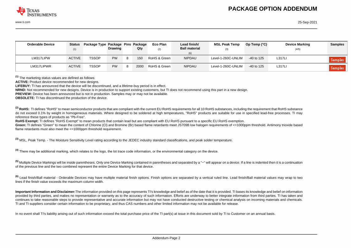
Orderable Device Status(1)
Package Type PackageDrawing
Pins PackageQty
Eco Plan(2)
Lead finish/Ball material
(6)
MSL Peak Temp(3)
Op Temp (°C) Device Marking(4/5)
Samples
LM317LIPW ACTIVE TSSOP PW 8 150 RoHS & Green NIPDAU Level-1-260C-UNLIM -40 to 125 L317LI
LM317LIPWR ACTIVE TSSOP PW 8 2000 RoHS & Green NIPDAU Level-1-260C-UNLIM -40 to 125 L317LI
(1) The marketing status values are defined as follows:ACTIVE: Product device recommended for new designs.LIFEBUY: TI has announced that the device will be discontinued, and a lifetime-buy period is in effect.NRND: Not recommended for new designs. Device is in production to support existing customers, but TI does not recommend using this part in a new design.PREVIEW: Device has been announced but is not in production. Samples may or may not be available.OBSOLETE: TI has discontinued the production of the device.
(2) RoHS: TI defines "RoHS" to mean semiconductor products that are compliant with the current EU RoHS requirements for all 10 RoHS substances, including the requirement that RoHS substancedo not exceed 0.1% by weight in homogeneous materials. Where designed to be soldered at high temperatures, "RoHS" products are suitable for use in specified lead-free processes. TI mayreference these types of products as "Pb-Free".RoHS Exempt: TI defines "RoHS Exempt" to mean products that contain lead but are compliant with EU RoHS pursuant to a specific EU RoHS exemption.Green: TI defines "Green" to mean the content of Chlorine (Cl) and Bromine (Br) based flame retardants meet JS709B low halogen requirements of <=1000ppm threshold. Antimony trioxide basedflame retardants must also meet the <=1000ppm threshold requirement.
(3) MSL, Peak Temp. - The Moisture Sensitivity Level rating according to the JEDEC industry standard classifications, and peak solder temperature.
(4) There may be additional marking, which relates to the logo, the lot trace code information, or the environmental category on the device.
(5) Multiple Device Markings will be inside parentheses. Only one Device Marking contained in parentheses and separated by a "~" will appear on a device. If a line is indented then it is a continuationof the previous line and the two combined represent the entire Device Marking for that device.
(6) Lead finish/Ball material - Orderable Devices may have multiple material finish options. Finish options are separated by a vertical ruled line. Lead finish/Ball material values may wrap to twolines if the finish value exceeds the maximum column width.
Important Information and Disclaimer:The information provided on this page represents TI's knowledge and belief as of the date that it is provided. TI bases its knowledge and belief on informationprovided by third parties, and makes no representation or warranty as to the accuracy of such information. Efforts are underway to better integrate information from third parties. TI has taken andcontinues to take reasonable steps to provide representative and accurate information but may not have conducted destructive testing or chemical analysis on incoming materials and chemicals.TI and TI suppliers consider certain information to be proprietary, and thus CAS numbers and other limited information may not be available for release.
In no event shall TI's liability arising out of such information exceed the total purchase price of the TI part(s) at issue in this document sold by TI to Customer on an annual basis.
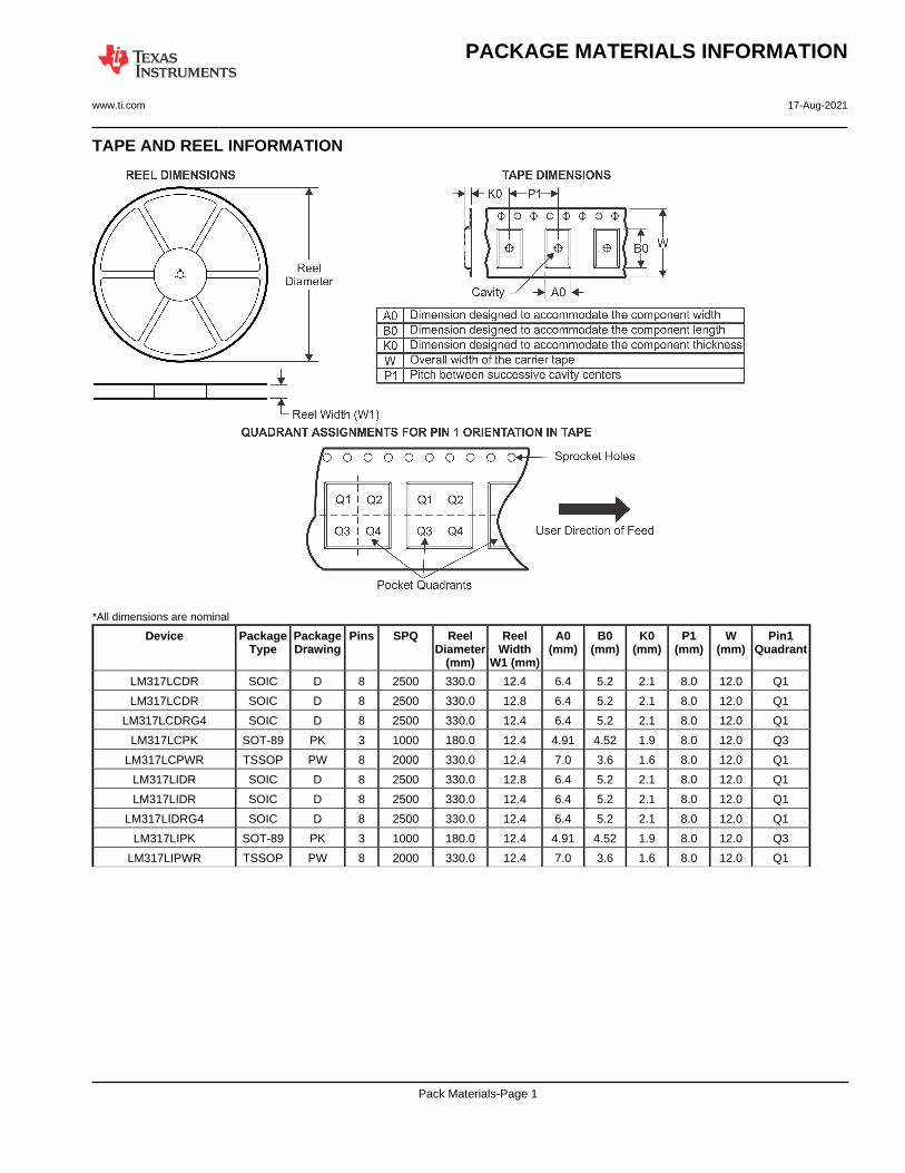
TAPE AND REEL INFORMATION
*All dimensions are nominal
Device PackageType
PackageDrawing
Pins SPQ ReelDiameter
(mm)
ReelWidth
W1 (mm)
A0(mm)
B0(mm)
K0(mm)
P1(mm)
W(mm)
Pin1Quadrant
LM317LCDR SOIC D 8 2500 330.0 12.4 6.4 5.2 2.1 8.0 12.0 Q1
LM317LCDR SOIC D 8 2500 330.0 12.8 6.4 5.2 2.1 8.0 12.0 Q1
LM317LCDRG4 SOIC D 8 2500 330.0 12.4 6.4 5.2 2.1 8.0 12.0 Q1
LM317LCPK SOT-89 PK 3 1000 180.0 12.4 4.91 4.52 1.9 8.0 12.0 Q3
LM317LCPWR TSSOP PW 8 2000 330.0 12.4 7.0 3.6 1.6 8.0 12.0 Q1
LM317LIDR SOIC D 8 2500 330.0 12.8 6.4 5.2 2.1 8.0 12.0 Q1
LM317LIDR SOIC D 8 2500 330.0 12.4 6.4 5.2 2.1 8.0 12.0 Q1
LM317LIDRG4 SOIC D 8 2500 330.0 12.4 6.4 5.2 2.1 8.0 12.0 Q1
LM317LIPK SOT-89 PK 3 1000 180.0 12.4 4.91 4.52 1.9 8.0 12.0 Q3
LM317LIPWR TSSOP PW 8 2000 330.0 12.4 7.0 3.6 1.6 8.0 12.0 Q1
PACKAGE MATERIALS INFORMATION
www.ti.com 17-Aug-2021
Pack Materials-Page 1
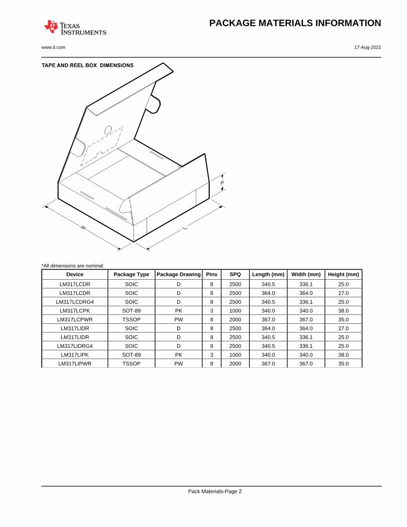
*All dimensions are nominal
Device Package Type Package Drawing Pins SPQ Length (mm) Width (mm) Height (mm)
LM317LCDR SOIC D 8 2500 340.5 336.1 25.0
LM317LCDR SOIC D 8 2500 364.0 364.0 27.0
LM317LCDRG4 SOIC D 8 2500 340.5 336.1 25.0
LM317LCPK SOT-89 PK 3 1000 340.0 340.0 38.0
LM317LCPWR TSSOP PW 8 2000 367.0 367.0 35.0
LM317LIDR SOIC D 8 2500 364.0 364.0 27.0
LM317LIDR SOIC D 8 2500 340.5 336.1 25.0
LM317LIDRG4 SOIC D 8 2500 340.5 336.1 25.0
LM317LIPK SOT-89 PK 3 1000 340.0 340.0 38.0
LM317LIPWR TSSOP PW 8 2000 367.0 367.0 35.0
PACKAGE MATERIALS INFORMATION
www.ti.com 17-Aug-2021
Pack Materials-Page 2
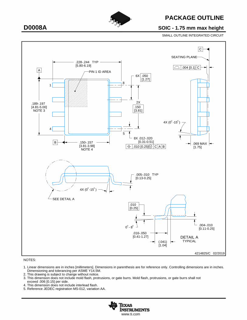
www.ti.com
PACKAGE OUTLINE
C
.228-.244 TYP[5.80-6.19]
.069 MAX[1.75]
6X .050[1.27]
8X .012-.020 [0.31-0.51]
2X.150[3.81]
.005-.010 TYP[0.13-0.25]
0 - 8 .004-.010[0.11-0.25]
.010[0.25]
.016-.050[0.41-1.27]
4X (0 -15 )
A
.189-.197[4.81-5.00]
NOTE 3
B .150-.157[3.81-3.98]
NOTE 4
4X (0 -15 )
(.041)[1.04]
SOIC - 1.75 mm max heightD0008ASMALL OUTLINE INTEGRATED CIRCUIT
4214825/C 02/2019
NOTES: 1. Linear dimensions are in inches [millimeters]. Dimensions in parenthesis are for reference only. Controlling dimensions are in inches. Dimensioning and tolerancing per ASME Y14.5M. 2. This drawing is subject to change without notice. 3. This dimension does not include mold flash, protrusions, or gate burrs. Mold flash, protrusions, or gate burrs shall not exceed .006 [0.15] per side. 4. This dimension does not include interlead flash.5. Reference JEDEC registration MS-012, variation AA.
18
.010 [0.25] C A B
54
PIN 1 ID AREA
SEATING PLANE
.004 [0.1] C
SEE DETAIL A
DETAIL ATYPICAL
SCALE 2.800
www.ti.com
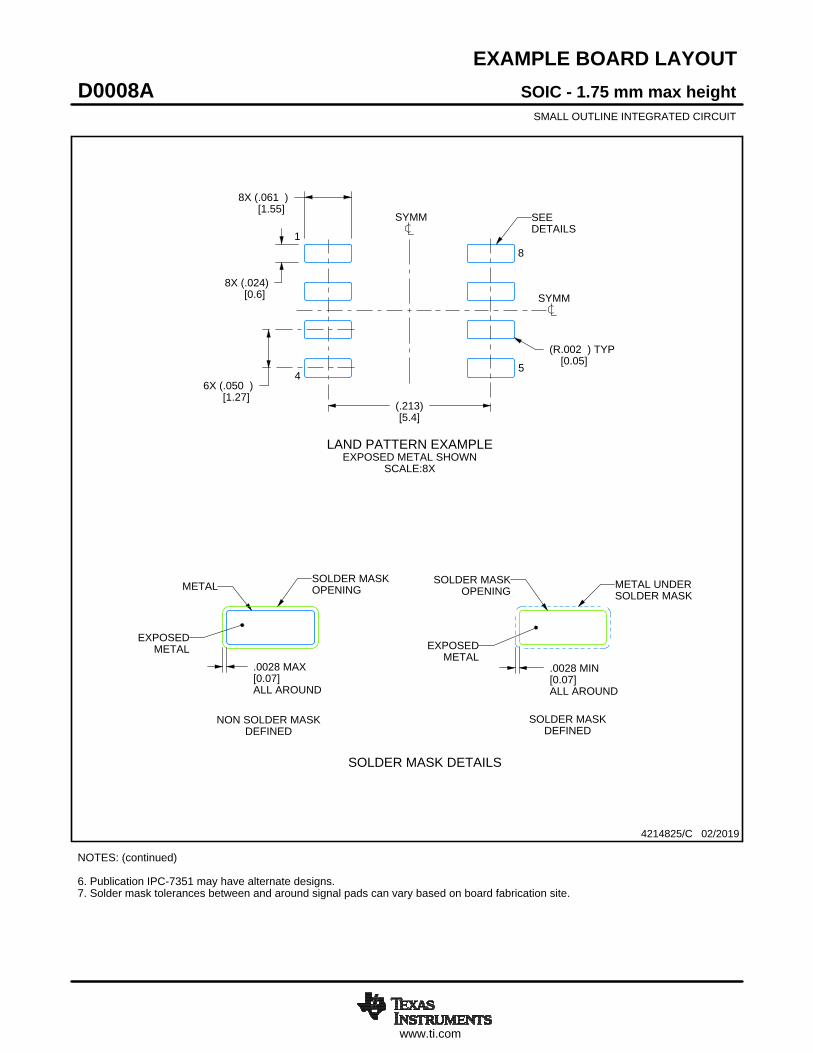
EXAMPLE BOARD LAYOUT
.0028 MAX[0.07]ALL AROUND
.0028 MIN[0.07]ALL AROUND
(.213)[5.4]
6X (.050 )[1.27]
8X (.061 )[1.55]
8X (.024)[0.6]
(R.002 ) TYP[0.05]
SOIC - 1.75 mm max heightD0008ASMALL OUTLINE INTEGRATED CIRCUIT
4214825/C 02/2019
NOTES: (continued) 6. Publication IPC-7351 may have alternate designs. 7. Solder mask tolerances between and around signal pads can vary based on board fabrication site.
METALSOLDER MASKOPENING
NON SOLDER MASKDEFINED
SOLDER MASK DETAILS
EXPOSEDMETAL
OPENINGSOLDER MASK METAL UNDER
SOLDER MASK
SOLDER MASKDEFINED
EXPOSEDMETAL
LAND PATTERN EXAMPLEEXPOSED METAL SHOWN
SCALE:8X
SYMM
1
45
8
SEEDETAILS
SYMM
www.ti.com
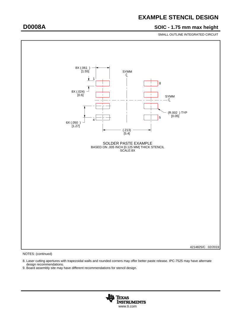
EXAMPLE STENCIL DESIGN
8X (.061 )[1.55]
8X (.024)[0.6]
6X (.050 )[1.27]
(.213)[5.4]
(R.002 ) TYP[0.05]
SOIC - 1.75 mm max heightD0008ASMALL OUTLINE INTEGRATED CIRCUIT
4214825/C 02/2019
NOTES: (continued) 8. Laser cutting apertures with trapezoidal walls and rounded corners may offer better paste release. IPC-7525 may have alternate design recommendations. 9. Board assembly site may have different recommendations for stencil design.
SOLDER PASTE EXAMPLEBASED ON .005 INCH [0.125 MM] THICK STENCIL
SCALE:8X
SYMM
SYMM
1
45
8
www.ti.com
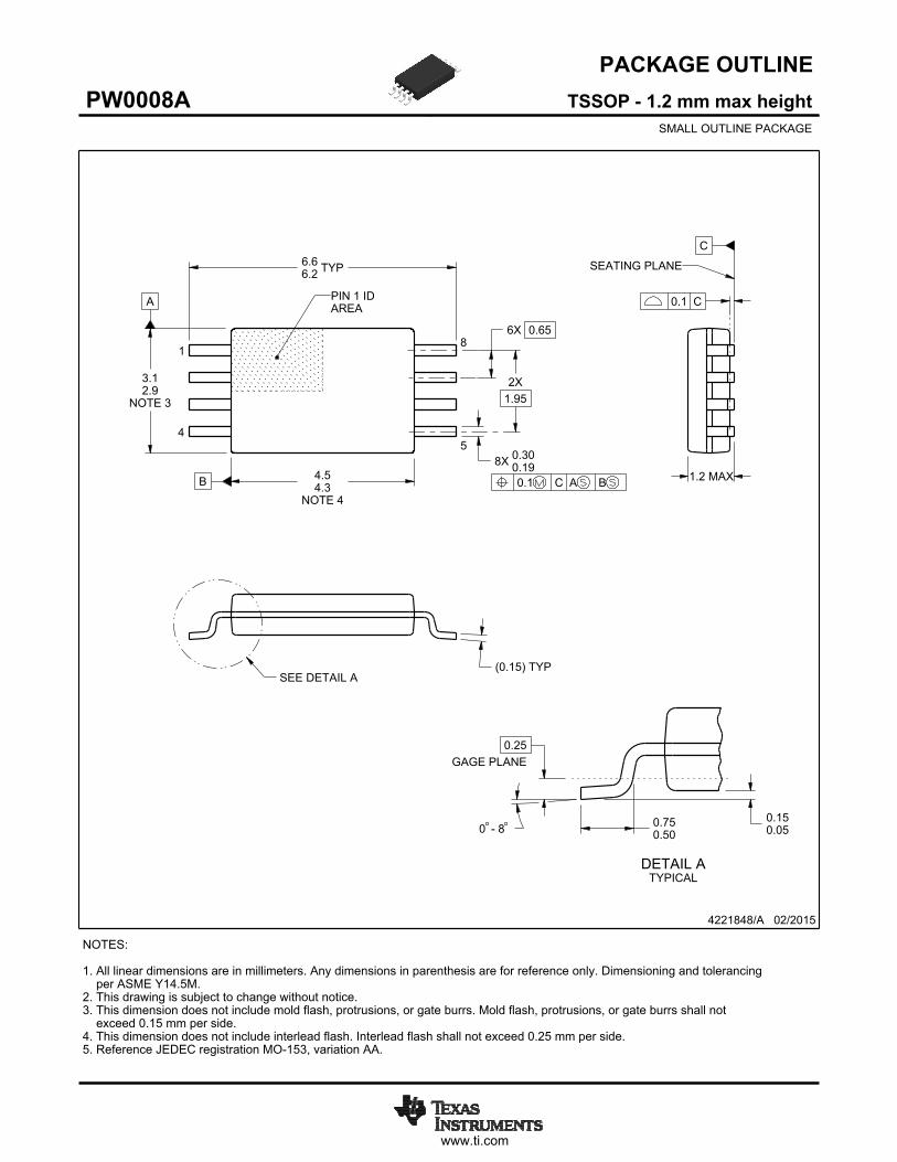
PACKAGE OUTLINE
C
TYP6.66.2
1.2 MAX
6X 0.65
8X 0.300.19
2X1.95
0.150.05
(0.15) TYP
0 - 8
0.25GAGE PLANE
0.750.50
A
NOTE 3
3.12.9
BNOTE 4
4.54.3
4221848/A 02/2015
TSSOP - 1.2 mm max heightPW0008ASMALL OUTLINE PACKAGE
NOTES: 1. All linear dimensions are in millimeters. Any dimensions in parenthesis are for reference only. Dimensioning and tolerancing per ASME Y14.5M. 2. This drawing is subject to change without notice. 3. This dimension does not include mold flash, protrusions, or gate burrs. Mold flash, protrusions, or gate burrs shall not exceed 0.15 mm per side. 4. This dimension does not include interlead flash. Interlead flash shall not exceed 0.25 mm per side.5. Reference JEDEC registration MO-153, variation AA.
18
0.1 C A B
54
PIN 1 IDAREA
SEATING PLANE
0.1 C
SEE DETAIL A
DETAIL ATYPICAL
SCALE 2.800
www.ti.com
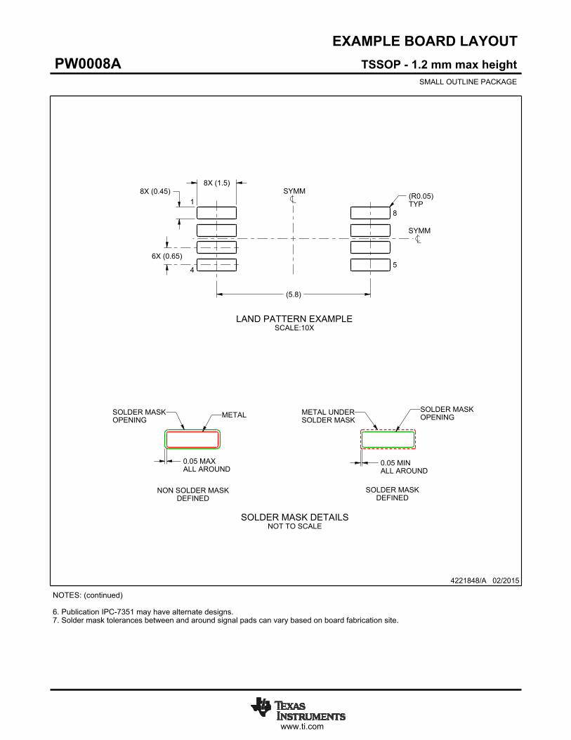
EXAMPLE BOARD LAYOUT
(5.8)
0.05 MAXALL AROUND
0.05 MINALL AROUND
8X (1.5)8X (0.45)
6X (0.65)
(R )TYP
0.05
4221848/A 02/2015
TSSOP - 1.2 mm max heightPW0008ASMALL OUTLINE PACKAGE
SYMM
SYMM
LAND PATTERN EXAMPLESCALE:10X
1
45
8
NOTES: (continued) 6. Publication IPC-7351 may have alternate designs. 7. Solder mask tolerances between and around signal pads can vary based on board fabrication site.
METALSOLDER MASKOPENING
NON SOLDER MASKDEFINED
SOLDER MASK DETAILSNOT TO SCALE
SOLDER MASKOPENING
METAL UNDERSOLDER MASK
SOLDER MASKDEFINED
www.ti.com
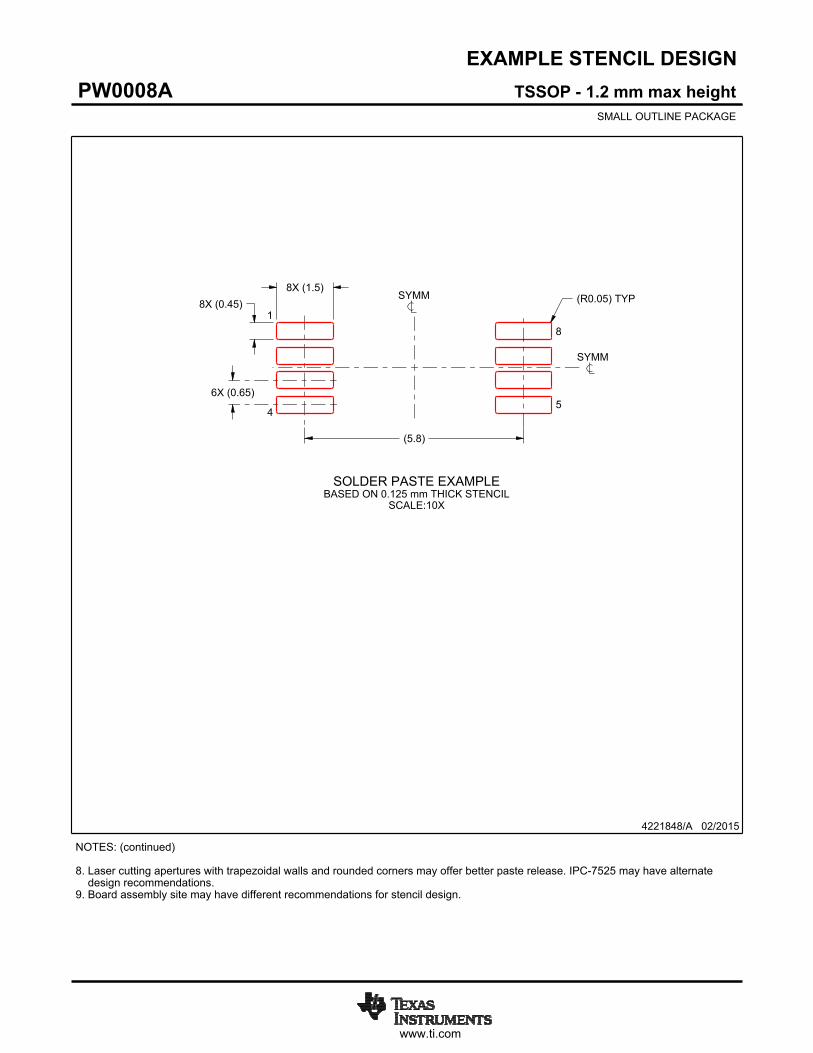
EXAMPLE STENCIL DESIGN
(5.8)
6X (0.65)
8X (0.45)8X (1.5)
(R ) TYP0.05
4221848/A 02/2015
TSSOP - 1.2 mm max heightPW0008ASMALL OUTLINE PACKAGE
NOTES: (continued) 8. Laser cutting apertures with trapezoidal walls and rounded corners may offer better paste release. IPC-7525 may have alternate design recommendations. 9. Board assembly site may have different recommendations for stencil design.
SYMM
SYMM
1
45
8
SOLDER PASTE EXAMPLEBASED ON 0.125 mm THICK STENCIL
SCALE:10X
www.ti.com
PACKAGE OUTLINE
3X 2.672.03
5.214.44
5.344.32
3X12.7 MIN
2X 1.27 0.13
3X 0.550.38
4.193.17
3.43 MIN
3X 0.430.35
(2.54)NOTE 3
2X2.6 0.2
2X4 MAX
SEATINGPLANE
6X0.076 MAX
(0.51) TYP
(1.5) TYP
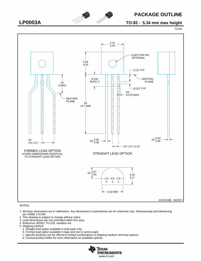
TO-92 - 5.34 mm max heightLP0003ATO-92
4215214/B 04/2017
NOTES: 1. All linear dimensions are in millimeters. Any dimensions in parenthesis are for reference only. Dimensioning and tolerancing per ASME Y14.5M.2. This drawing is subject to change without notice.3. Lead dimensions are not controlled within this area.4. Reference JEDEC TO-226, variation AA.5. Shipping method: a. Straight lead option available in bulk pack only. b. Formed lead option available in tape and reel or ammo pack. c. Specific products can be offered in limited combinations of shipping medium and lead options. d. Consult product folder for more information on available options.
EJECTOR PINOPTIONAL
PLANESEATING
STRAIGHT LEAD OPTION
3 2 1
SCALE 1.200
FORMED LEAD OPTIONOTHER DIMENSIONS IDENTICAL
TO STRAIGHT LEAD OPTION
SCALE 1.200
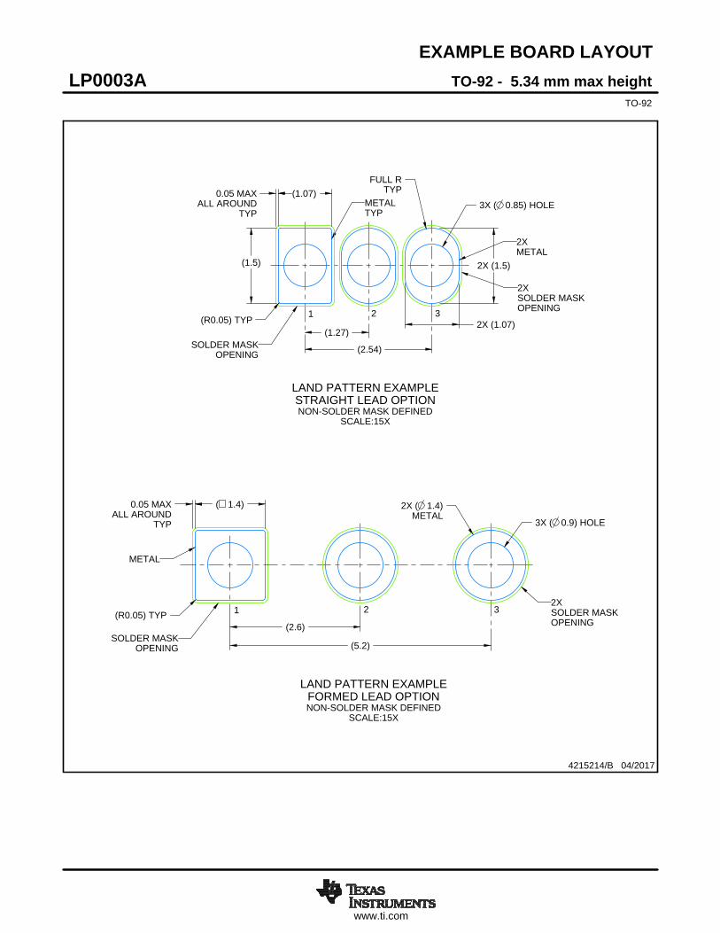
www.ti.com
EXAMPLE BOARD LAYOUT
0.05 MAXALL AROUND
TYP
(1.07)
(1.5) 2X (1.5)
2X (1.07)(1.27)
(2.54)
FULL RTYP
( 1.4)0.05 MAXALL AROUND
TYP
(2.6)
(5.2)
(R0.05) TYP
3X ( 0.9) HOLE
2X ( 1.4)METAL
3X ( 0.85) HOLE
(R0.05) TYP
4215214/B 04/2017
TO-92 - 5.34 mm max heightLP0003ATO-92
LAND PATTERN EXAMPLEFORMED LEAD OPTIONNON-SOLDER MASK DEFINED
SCALE:15X
SOLDER MASKOPENING
METAL
2XSOLDER MASKOPENING
1 2 3
LAND PATTERN EXAMPLESTRAIGHT LEAD OPTIONNON-SOLDER MASK DEFINED
SCALE:15X
METALTYP
SOLDER MASKOPENING
2XSOLDER MASKOPENING
2XMETAL
1 2 3
www.ti.com
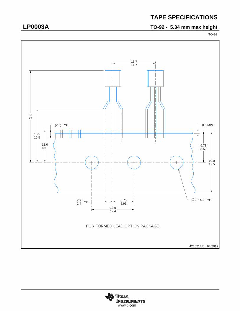
TAPE SPECIFICATIONS
19.017.5
13.711.7
11.08.5
0.5 MIN
TYP-4.33.7
9.758.50
TYP2.92.4
6.755.95
13.012.4
(2.5) TYP
16.515.5
3223
4215214/B 04/2017
TO-92 - 5.34 mm max heightLP0003ATO-92
FOR FORMED LEAD OPTION PACKAGE

IMPORTANT NOTICE AND DISCLAIMERTI PROVIDES TECHNICAL AND RELIABILITY DATA (INCLUDING DATASHEETS), DESIGN RESOURCES (INCLUDING REFERENCEDESIGNS), APPLICATION OR OTHER DESIGN ADVICE, WEB TOOLS, SAFETY INFORMATION, AND OTHER RESOURCES “AS IS”AND WITH ALL FAULTS, AND DISCLAIMS ALL WARRANTIES, EXPRESS AND IMPLIED, INCLUDING WITHOUT LIMITATION ANYIMPLIED WARRANTIES OF MERCHANTABILITY, FITNESS FOR A PARTICULAR PURPOSE OR NON-INFRINGEMENT OF THIRDPARTY INTELLECTUAL PROPERTY RIGHTS.These resources are intended for skilled developers designing with TI products. You are solely responsible for (1) selecting the appropriateTI products for your application, (2) designing, validating and testing your application, and (3) ensuring your application meets applicablestandards, and any other safety, security, or other requirements. These resources are subject to change without notice. TI grants youpermission to use these resources only for development of an application that uses the TI products described in the resource. Otherreproduction and display of these resources is prohibited. No license is granted to any other TI intellectual property right or to any third partyintellectual property right. TI disclaims responsibility for, and you will fully indemnify TI and its representatives against, any claims, damages,costs, losses, and liabilities arising out of your use of these resources.TI’s products are provided subject to TI’s Terms of Sale (https:www.ti.com/legal/termsofsale.html) or other applicable terms available eitheron ti.com or provided in conjunction with such TI products. TI’s provision of these resources does not expand or otherwise alter TI’sapplicable warranties or warranty disclaimers for TI products.IMPORTANT NOTICE
Mailing Address: Texas Instruments, Post Office Box 655303, Dallas, Texas 75265Copyright © 2021, Texas Instruments Incorporated