Embed Size (px)
Citation preview
Product
Folder
Order
Now
Technical
Documents
Tools &
Software
Support &Community
An IMPORTANT NOTICE at the end of this data sheet addresses availability, warranty, changes, use in safety-critical applications,intellectual property matters and other important disclaimers. PRODUCTION DATA.
LM317L-NSNVS775L –MARCH 2000–REVISED JANUARY 2018
LM317L-N Wide VIN 100-mA Adjustable Voltage Regulator
1
1 Features1• Adjustable Output Down to 1.2 V• 100-mA Output Current• Capable of Handling up to 40V VIN
• Line Regulation Typically 0.01% /V• Load Regulation Typically 0.1% /A• No Output Capacitor Required (†)• Current Limit Constant With Temperature• Eliminates the Need to Stock Many Voltages• Standard 3-Lead Transistor Package• 80-dB Ripple Rejection• Available in 3-Pin TO-92, 8-Pin SOIC, or 6-pin
DSBGA Packages• Output is Short-Circuit Protected• See AN-1112 (SNVA009) for DSBGA
Considerations
2 Applications• Automotive LED Lighting• Battery Chargers• Post Regulation for Switching Supplies• Constant-Current Regulators• Microprocessor Supplies
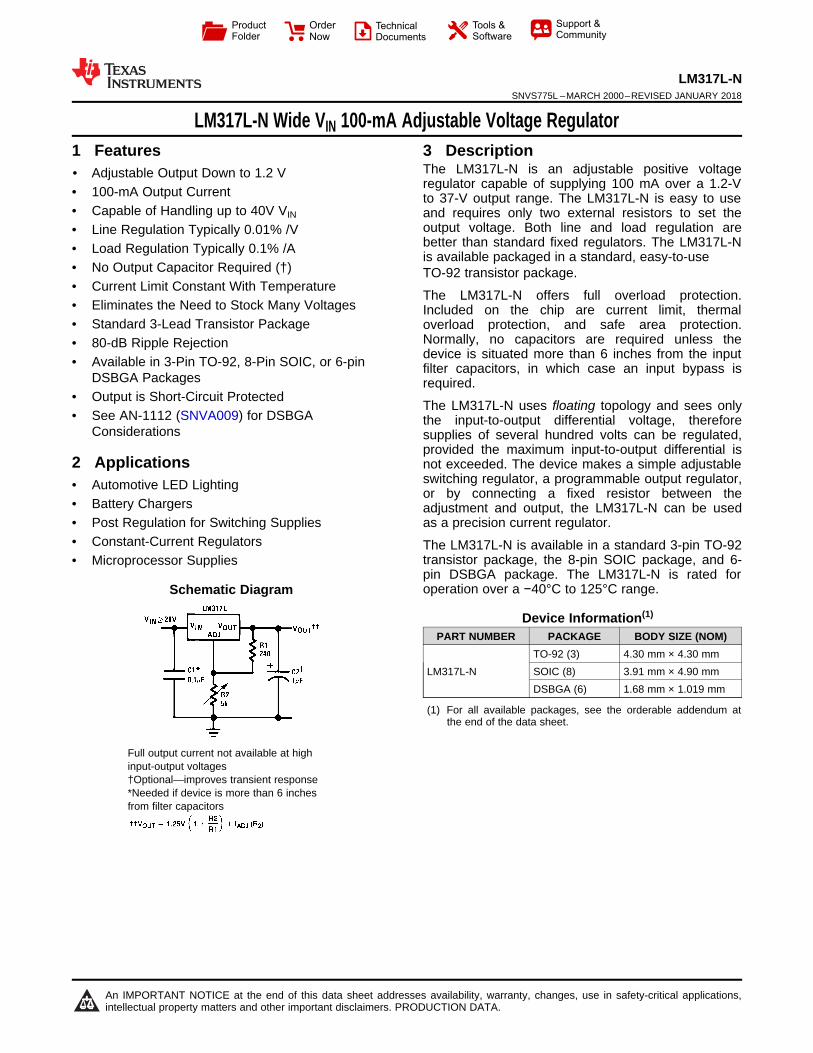
Schematic Diagram
Full output current not available at highinput-output voltages†Optional—improves transient response*Needed if device is more than 6 inchesfrom filter capacitors
3 DescriptionThe LM317L-N is an adjustable positive voltageregulator capable of supplying 100 mA over a 1.2-Vto 37-V output range. The LM317L-N is easy to useand requires only two external resistors to set theoutput voltage. Both line and load regulation arebetter than standard fixed regulators. The LM317L-Nis available packaged in a standard, easy-to-useTO-92 transistor package.
The LM317L-N offers full overload protection.Included on the chip are current limit, thermaloverload protection, and safe area protection.Normally, no capacitors are required unless thedevice is situated more than 6 inches from the inputfilter capacitors, in which case an input bypass isrequired.
The LM317L-N uses floating topology and sees onlythe input-to-output differential voltage, thereforesupplies of several hundred volts can be regulated,provided the maximum input-to-output differential isnot exceeded. The device makes a simple adjustableswitching regulator, a programmable output regulator,or by connecting a fixed resistor between theadjustment and output, the LM317L-N can be usedas a precision current regulator.
The LM317L-N is available in a standard 3-pin TO-92transistor package, the 8-pin SOIC package, and 6-pin DSBGA package. The LM317L-N is rated foroperation over a −40°C to 125°C range.
Device Information(1)
PART NUMBER PACKAGE BODY SIZE (NOM)
LM317L-NTO-92 (3) 4.30 mm × 4.30 mmSOIC (8) 3.91 mm × 4.90 mmDSBGA (6) 1.68 mm × 1.019 mm
(1) For all available packages, see the orderable addendum atthe end of the data sheet.
2
LM317L-NSNVS775L –MARCH 2000–REVISED JANUARY 2018 www.ti.com
Product Folder Links: LM317L-N
Submit Documentation Feedback Copyright © 2000–2018, Texas Instruments Incorporated
Table of Contents1 Features .................................................................. 12 Applications ........................................................... 13 Description ............................................................. 14 Revision History..................................................... 25 Pin Configuration and Functions ......................... 36 Specifications......................................................... 4
6.1 Absolute Maximum Rating ....................................... 46.2 ESD Ratings.............................................................. 46.3 Recommended Operating Conditions....................... 46.4 Thermal Information .................................................. 46.5 Electrical Characteristics .......................................... 56.6 Typical Characteristics .............................................. 6
7 Detailed Description .............................................. 87.1 Overview ................................................................... 87.2 Functional Block Diagram ......................................... 97.3 Feature Description................................................. 10
7.4 Device Functional Modes........................................ 108 Application and Implementation ........................ 12
8.1 Application Information............................................ 128.2 Typical Applications ............................................... 12
9 Power Supply Recommendations ...................... 2510 Layout................................................................... 25
10.1 Layout Guidelines ................................................. 2510.2 Layout Examples................................................... 2510.3 Thermal Considerations ........................................ 26
11 Device and Documentation Support ................. 2711.1 Documentation Support ........................................ 2711.2 Community Resources.......................................... 2711.3 Trademarks ........................................................... 2711.4 Electrostatic Discharge Caution............................ 2711.5 Glossary ................................................................ 27
12 Mechanical, Packaging, and OrderableInformation ........................................................... 27
4 Revision HistoryNOTE: Page numbers for previous revisions may differ from page numbers in the current version.
Changes from Revision K (September 2015) to Revision L Page
• Changed TO-92 package view from top to bottom view ........................................................................................................ 3• Changed DSBGA package view from bump side down to top view ...................................................................................... 3• Removed duplicate Protection Diodes section and Regulator With Protection Diodes image from the Device
Functional Modes section..................................................................................................................................................... 10
Changes from Revision J (March 2013) to Revision K Page
• Added ESD Ratings table, Feature Description section, Device Functional Modes, Application and Implementationsection, Power Supply Recommendations section, Layout section, Device and Documentation Support section, andMechanical, Packaging, and Orderable Information section. ................................................................................................ 1
Changes from Revision I (March 2013) to Revision J Page
• Changed layout of National Data Sheet to TI format ........................................................................................................... 25
3
LM317L-Nwww.ti.com SNVS775L –MARCH 2000–REVISED JANUARY 2018
Product Folder Links: LM317L-N
Submit Documentation FeedbackCopyright © 2000–2018, Texas Instruments Incorporated
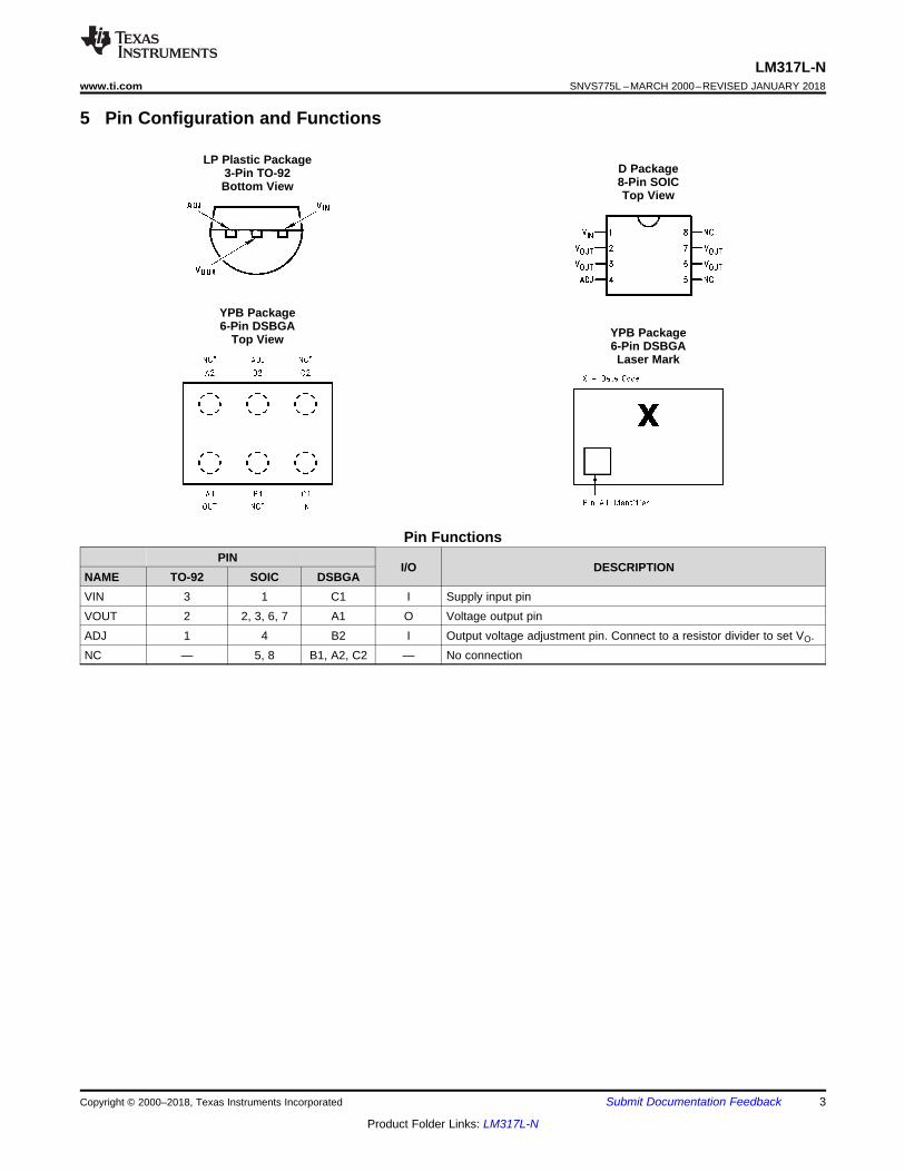
5 Pin Configuration and Functions
LP Plastic Package3-Pin TO-92Bottom View
YPB Package6-Pin DSBGA
Top View
D Package8-Pin SOICTop View
YPB Package6-Pin DSBGALaser Mark
Pin FunctionsPIN
I/O DESCRIPTIONNAME TO-92 SOIC DSBGAVIN 3 1 C1 I Supply input pinVOUT 2 2, 3, 6, 7 A1 O Voltage output pinADJ 1 4 B2 I Output voltage adjustment pin. Connect to a resistor divider to set VO.NC — 5, 8 B1, A2, C2 — No connection
4
LM317L-NSNVS775L –MARCH 2000–REVISED JANUARY 2018 www.ti.com
Product Folder Links: LM317L-N
Submit Documentation Feedback Copyright © 2000–2018, Texas Instruments Incorporated
(1) Stresses beyond those listed under Absolute Maximum Ratings may cause permanent damage to the device. These are stress ratingsonly, which do not imply functional operation of the device at these or any other conditions beyond those indicated under RecommendedOperating Conditions. Exposure to absolute-maximum-rated conditions for extended periods may affect device reliability.
(2) If Military/Aerospace specified devices are required, contact the Texas Instruments Sales Office/Distributors for availability andspecifications.
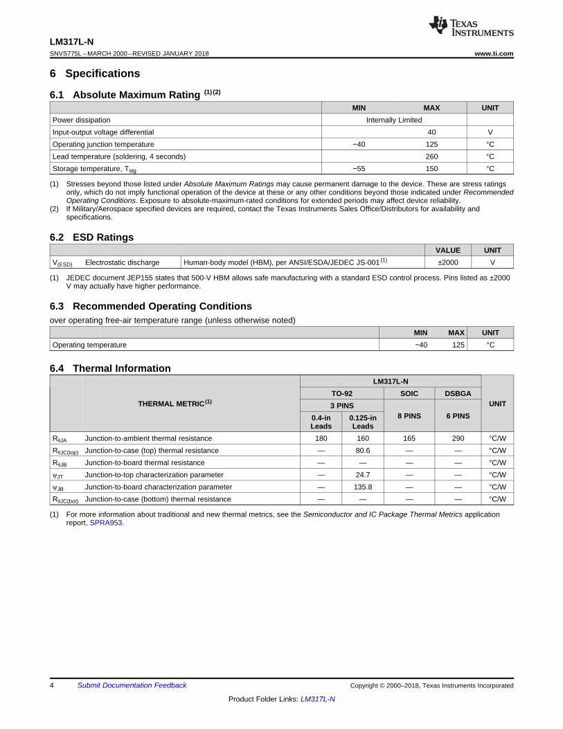
6 Specifications
6.1 Absolute Maximum Rating (1) (2)
MIN MAX UNITPower dissipation Internally LimitedInput-output voltage differential 40 VOperating junction temperature −40 125 °CLead temperature (soldering, 4 seconds) 260 °CStorage temperature, Tstg −55 150 °C
(1) JEDEC document JEP155 states that 500-V HBM allows safe manufacturing with a standard ESD control process. Pins listed as ±2000V may actually have higher performance.
6.2 ESD RatingsVALUE UNIT
V(ESD) Electrostatic discharge Human-body model (HBM), per ANSI/ESDA/JEDEC JS-001 (1) ±2000 V
6.3 Recommended Operating Conditionsover operating free-air temperature range (unless otherwise noted)
MIN MAX UNITOperating temperature −40 125 °C
(1) For more information about traditional and new thermal metrics, see the Semiconductor and IC Package Thermal Metrics applicationreport, SPRA953.
6.4 Thermal Information
THERMAL METRIC (1)
LM317L-N
UNITTO-92 SOIC DSBGA3 PINS
8 PINS 6 PINS0.4-inLeads
0.125-inLeads
RθJA Junction-to-ambient thermal resistance 180 160 165 290 °C/WRθJC(top) Junction-to-case (top) thermal resistance — 80.6 — — °C/WRθJB Junction-to-board thermal resistance — — — — °C/WψJT Junction-to-top characterization parameter — 24.7 — — °C/WψJB Junction-to-board characterization parameter — 135.8 — — °C/WRθJC(bot) Junction-to-case (bottom) thermal resistance — — — — °C/W
5
LM317L-Nwww.ti.com SNVS775L –MARCH 2000–REVISED JANUARY 2018
Product Folder Links: LM317L-N
Submit Documentation FeedbackCopyright © 2000–2018, Texas Instruments Incorporated
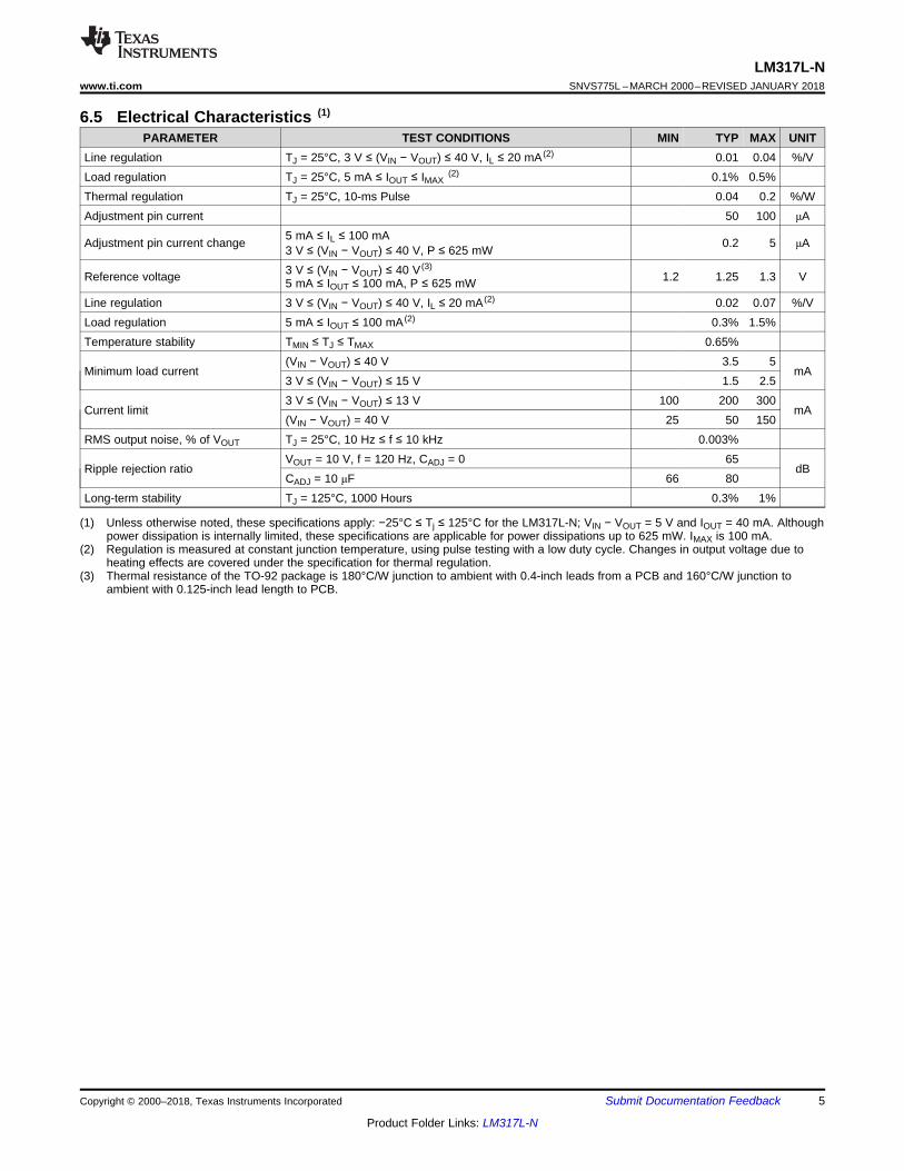
(1) Unless otherwise noted, these specifications apply: −25°C ≤ Tj ≤ 125°C for the LM317L-N; VIN − VOUT = 5 V and IOUT = 40 mA. Althoughpower dissipation is internally limited, these specifications are applicable for power dissipations up to 625 mW. IMAX is 100 mA.
(2) Regulation is measured at constant junction temperature, using pulse testing with a low duty cycle. Changes in output voltage due toheating effects are covered under the specification for thermal regulation.
(3) Thermal resistance of the TO-92 package is 180°C/W junction to ambient with 0.4-inch leads from a PCB and 160°C/W junction toambient with 0.125-inch lead length to PCB.
6.5 Electrical Characteristics (1)
PARAMETER TEST CONDITIONS MIN TYP MAX UNITLine regulation TJ = 25°C, 3 V ≤ (VIN − VOUT) ≤ 40 V, IL ≤ 20 mA (2) 0.01 0.04 %/VLoad regulation TJ = 25°C, 5 mA ≤ IOUT ≤ IMAX
(2) 0.1% 0.5%Thermal regulation TJ = 25°C, 10-ms Pulse 0.04 0.2 %/WAdjustment pin current 50 100 μA
Adjustment pin current change 5 mA ≤ IL ≤ 100 mA3 V ≤ (VIN − VOUT) ≤ 40 V, P ≤ 625 mW 0.2 5 μA
Reference voltage 3 V ≤ (VIN − VOUT) ≤ 40 V (3)
5 mA ≤ IOUT ≤ 100 mA, P ≤ 625 mW 1.2 1.25 1.3 V
Line regulation 3 V ≤ (VIN − VOUT) ≤ 40 V, IL ≤ 20 mA (2) 0.02 0.07 %/VLoad regulation 5 mA ≤ IOUT ≤ 100 mA (2) 0.3% 1.5%Temperature stability TMIN ≤ TJ ≤ TMAX 0.65%
Minimum load current(VIN − VOUT) ≤ 40 V 3.5 5
mA3 V ≤ (VIN − VOUT) ≤ 15 V 1.5 2.5
Current limit3 V ≤ (VIN − VOUT) ≤ 13 V 100 200 300
mA(VIN − VOUT) = 40 V 25 50 150
RMS output noise, % of VOUT TJ = 25°C, 10 Hz ≤ f ≤ 10 kHz 0.003%
Ripple rejection ratioVOUT = 10 V, f = 120 Hz, CADJ = 0 65
dBCADJ = 10 μF 66 80
Long-term stability TJ = 125°C, 1000 Hours 0.3% 1%
6
LM317L-NSNVS775L –MARCH 2000–REVISED JANUARY 2018 www.ti.com
Product Folder Links: LM317L-N
Submit Documentation Feedback Copyright © 2000–2018, Texas Instruments Incorporated
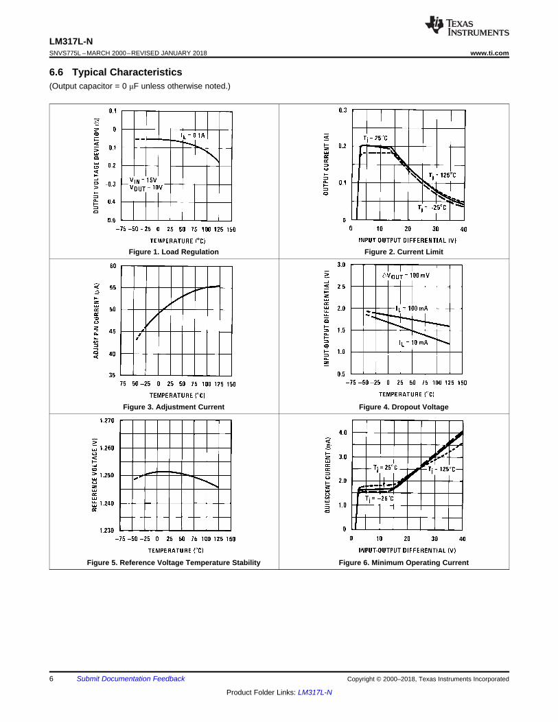
6.6 Typical Characteristics(Output capacitor = 0 μF unless otherwise noted.)
Figure 1. Load Regulation Figure 2. Current Limit
Figure 3. Adjustment Current Figure 4. Dropout Voltage
Figure 5. Reference Voltage Temperature Stability Figure 6. Minimum Operating Current
7
LM317L-Nwww.ti.com SNVS775L –MARCH 2000–REVISED JANUARY 2018
Product Folder Links: LM317L-N
Submit Documentation FeedbackCopyright © 2000–2018, Texas Instruments Incorporated
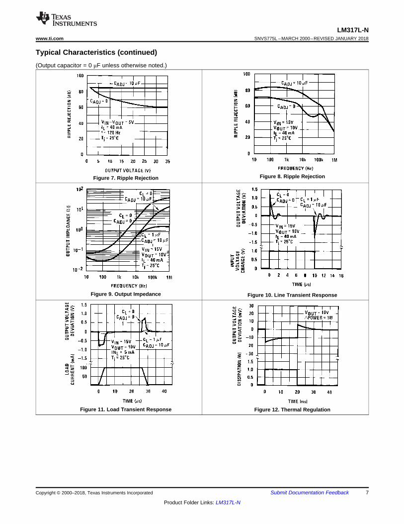
Typical Characteristics (continued)(Output capacitor = 0 μF unless otherwise noted.)
Figure 7. Ripple Rejection Figure 8. Ripple Rejection
Figure 9. Output Impedance Figure 10. Line Transient Response
Figure 11. Load Transient Response Figure 12. Thermal Regulation
8
LM317L-NSNVS775L –MARCH 2000–REVISED JANUARY 2018 www.ti.com
Product Folder Links: LM317L-N
Submit Documentation Feedback Copyright © 2000–2018, Texas Instruments Incorporated
7 Detailed Description
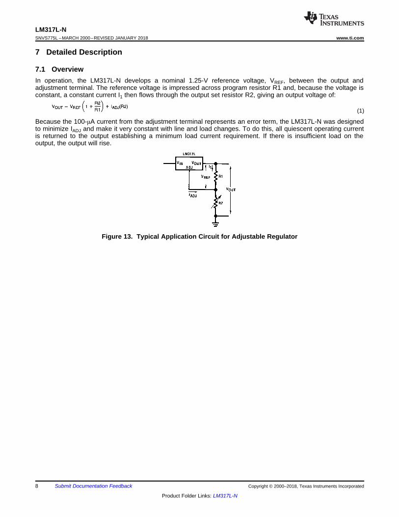
7.1 OverviewIn operation, the LM317L-N develops a nominal 1.25-V reference voltage, VREF, between the output andadjustment terminal. The reference voltage is impressed across program resistor R1 and, because the voltage isconstant, a constant current I1 then flows through the output set resistor R2, giving an output voltage of:
(1)
Because the 100-μA current from the adjustment terminal represents an error term, the LM317L-N was designedto minimize IADJ and make it very constant with line and load changes. To do this, all quiescent operating currentis returned to the output establishing a minimum load current requirement. If there is insufficient load on theoutput, the output will rise.
Figure 13. Typical Application Circuit for Adjustable Regulator
LM317L-Nwww.ti.com SNVS775L –MARCH 2000–REVISED JANUARY 2018
9
Product Folder Links: LM317L-N
Submit Documentation FeedbackCopyright © 2000–2018, Texas Instruments Incorporated
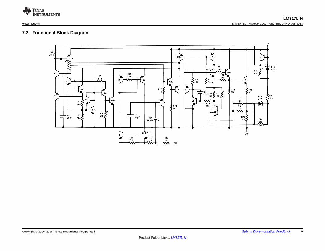
7.2 Functional Block Diagram
10
LM317L-NSNVS775L –MARCH 2000–REVISED JANUARY 2018 www.ti.com
Product Folder Links: LM317L-N
Submit Documentation Feedback Copyright © 2000–2018, Texas Instruments Incorporated
7.3 Feature Description
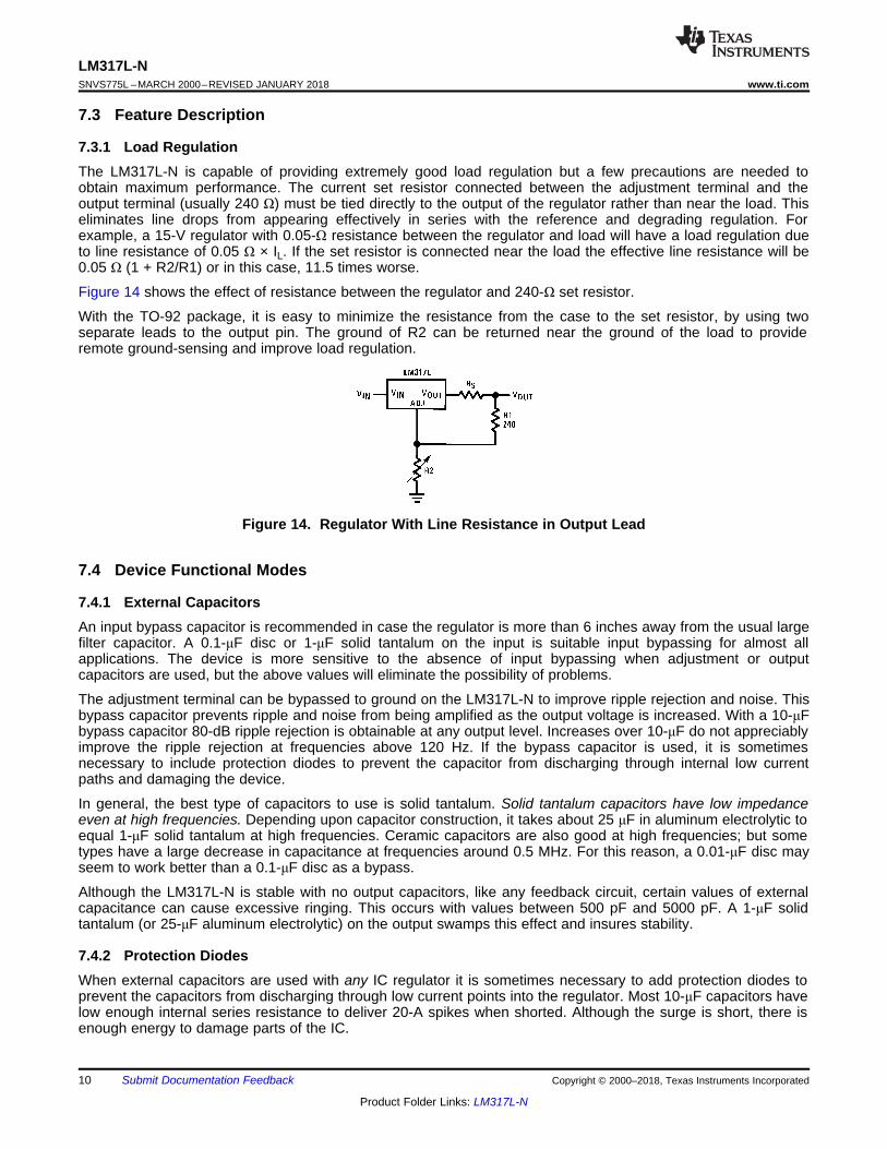
7.3.1 Load RegulationThe LM317L-N is capable of providing extremely good load regulation but a few precautions are needed toobtain maximum performance. The current set resistor connected between the adjustment terminal and theoutput terminal (usually 240 Ω) must be tied directly to the output of the regulator rather than near the load. Thiseliminates line drops from appearing effectively in series with the reference and degrading regulation. Forexample, a 15-V regulator with 0.05-Ω resistance between the regulator and load will have a load regulation dueto line resistance of 0.05 Ω × IL. If the set resistor is connected near the load the effective line resistance will be0.05 Ω (1 + R2/R1) or in this case, 11.5 times worse.
Figure 14 shows the effect of resistance between the regulator and 240-Ω set resistor.
With the TO-92 package, it is easy to minimize the resistance from the case to the set resistor, by using twoseparate leads to the output pin. The ground of R2 can be returned near the ground of the load to provideremote ground-sensing and improve load regulation.
Figure 14. Regulator With Line Resistance in Output Lead
7.4 Device Functional Modes
7.4.1 External CapacitorsAn input bypass capacitor is recommended in case the regulator is more than 6 inches away from the usual largefilter capacitor. A 0.1-μF disc or 1-μF solid tantalum on the input is suitable input bypassing for almost allapplications. The device is more sensitive to the absence of input bypassing when adjustment or outputcapacitors are used, but the above values will eliminate the possibility of problems.
The adjustment terminal can be bypassed to ground on the LM317L-N to improve ripple rejection and noise. Thisbypass capacitor prevents ripple and noise from being amplified as the output voltage is increased. With a 10-μFbypass capacitor 80-dB ripple rejection is obtainable at any output level. Increases over 10-μF do not appreciablyimprove the ripple rejection at frequencies above 120 Hz. If the bypass capacitor is used, it is sometimesnecessary to include protection diodes to prevent the capacitor from discharging through internal low currentpaths and damaging the device.
In general, the best type of capacitors to use is solid tantalum. Solid tantalum capacitors have low impedanceeven at high frequencies. Depending upon capacitor construction, it takes about 25 μF in aluminum electrolytic toequal 1-μF solid tantalum at high frequencies. Ceramic capacitors are also good at high frequencies; but sometypes have a large decrease in capacitance at frequencies around 0.5 MHz. For this reason, a 0.01-μF disc mayseem to work better than a 0.1-μF disc as a bypass.
Although the LM317L-N is stable with no output capacitors, like any feedback circuit, certain values of externalcapacitance can cause excessive ringing. This occurs with values between 500 pF and 5000 pF. A 1-μF solidtantalum (or 25-μF aluminum electrolytic) on the output swamps this effect and insures stability.
7.4.2 Protection DiodesWhen external capacitors are used with any IC regulator it is sometimes necessary to add protection diodes toprevent the capacitors from discharging through low current points into the regulator. Most 10-μF capacitors havelow enough internal series resistance to deliver 20-A spikes when shorted. Although the surge is short, there isenough energy to damage parts of the IC.
11
LM317L-Nwww.ti.com SNVS775L –MARCH 2000–REVISED JANUARY 2018
Product Folder Links: LM317L-N
Submit Documentation FeedbackCopyright © 2000–2018, Texas Instruments Incorporated
Device Functional Modes (continued)When an output capacitor is connected to a regulator and the input is shorted, the output capacitor will dischargeinto the output of the regulator. The discharge current depends on the value of the capacitor, the output voltageof the regulator, and the rate of decrease of VIN. In the LM317L-N, this discharge path is through a large junctionthat is able to sustain a 2-A surge with no problem. This is not true of other types of positive regulators. Foroutput capacitors of 25 μF or less, the ballast resistors and output structure of the LM317L-N limit the peakcurrent to a low enough level so that there is no need to use a protection diode.
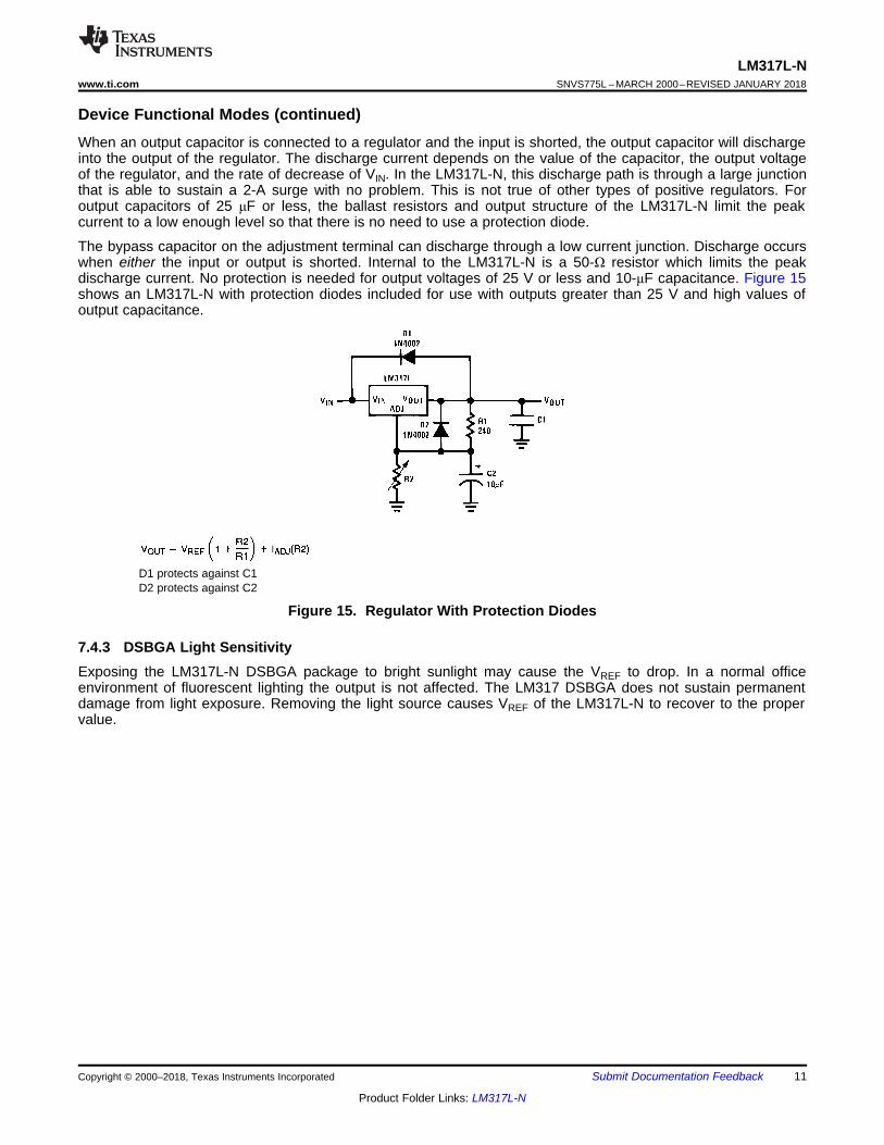
The bypass capacitor on the adjustment terminal can discharge through a low current junction. Discharge occurswhen either the input or output is shorted. Internal to the LM317L-N is a 50-Ω resistor which limits the peakdischarge current. No protection is needed for output voltages of 25 V or less and 10-μF capacitance. Figure 15shows an LM317L-N with protection diodes included for use with outputs greater than 25 V and high values ofoutput capacitance.
D1 protects against C1D2 protects against C2
Figure 15. Regulator With Protection Diodes
7.4.3 DSBGA Light SensitivityExposing the LM317L-N DSBGA package to bright sunlight may cause the VREF to drop. In a normal officeenvironment of fluorescent lighting the output is not affected. The LM317 DSBGA does not sustain permanentdamage from light exposure. Removing the light source causes VREF of the LM317L-N to recover to the propervalue.
12
LM317L-NSNVS775L –MARCH 2000–REVISED JANUARY 2018 www.ti.com
Product Folder Links: LM317L-N
Submit Documentation Feedback Copyright © 2000–2018, Texas Instruments Incorporated
8 Application and Implementation
NOTEInformation in the following applications sections is not part of the TI componentspecification, and TI does not warrant its accuracy or completeness. TI’s customers areresponsible for determining suitability of components for their purposes. Customers shouldvalidate and test their design implementation to confirm system functionality.
8.1 Application InformationThe LM317L-N is a versatile, high-performance, linear regulator with 1% output-voltage accuracy. An outputcapacitor can be added to further improve transient response, and the ADJ pin can be bypassed to achieve veryhigh ripple-rejection ratios. Its functionality can be used in many different applications that require highperformance regulation, such as battery chargers, constant-current regulators, and microprocessor supplies.
8.2 Typical Applications
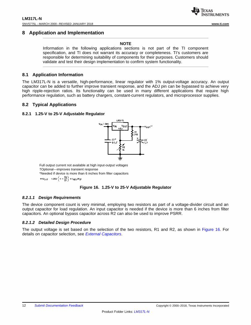
8.2.1 1.25-V to 25-V Adjustable Regulator
Full output current not available at high input-output voltages†Optional—improves transient response*Needed if device is more than 6 inches from filter capacitors
Figure 16. 1.25-V to 25-V Adjustable Regulator
8.2.1.1 Design RequirementsThe device component count is very minimal, employing two resistors as part of a voltage-divider circuit and anoutput capacitor for load regulation. An input capacitor is needed if the device is more than 6 inches from filtercapacitors. An optional bypass capacitor across R2 can also be used to improve PSRR.
8.2.1.2 Detailed Design ProcedureThe output voltage is set based on the selection of the two resistors, R1 and R2, as shown in Figure 16. Fordetails on capacitor selection, see External Capacitors.
13
LM317L-Nwww.ti.com SNVS775L –MARCH 2000–REVISED JANUARY 2018
Product Folder Links: LM317L-N
Submit Documentation FeedbackCopyright © 2000–2018, Texas Instruments Incorporated
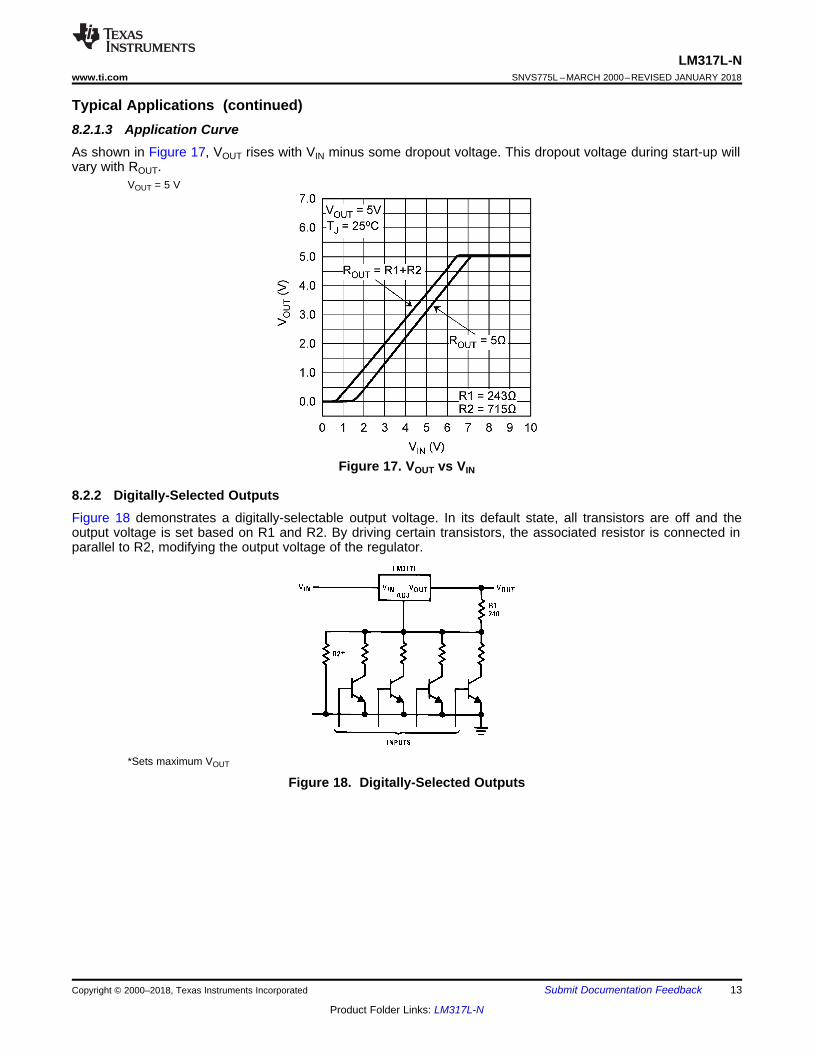
Typical Applications (continued)8.2.1.3 Application CurveAs shown in Figure 17, VOUT rises with VIN minus some dropout voltage. This dropout voltage during start-up willvary with ROUT.
VOUT = 5 V
Figure 17. VOUT vs VIN
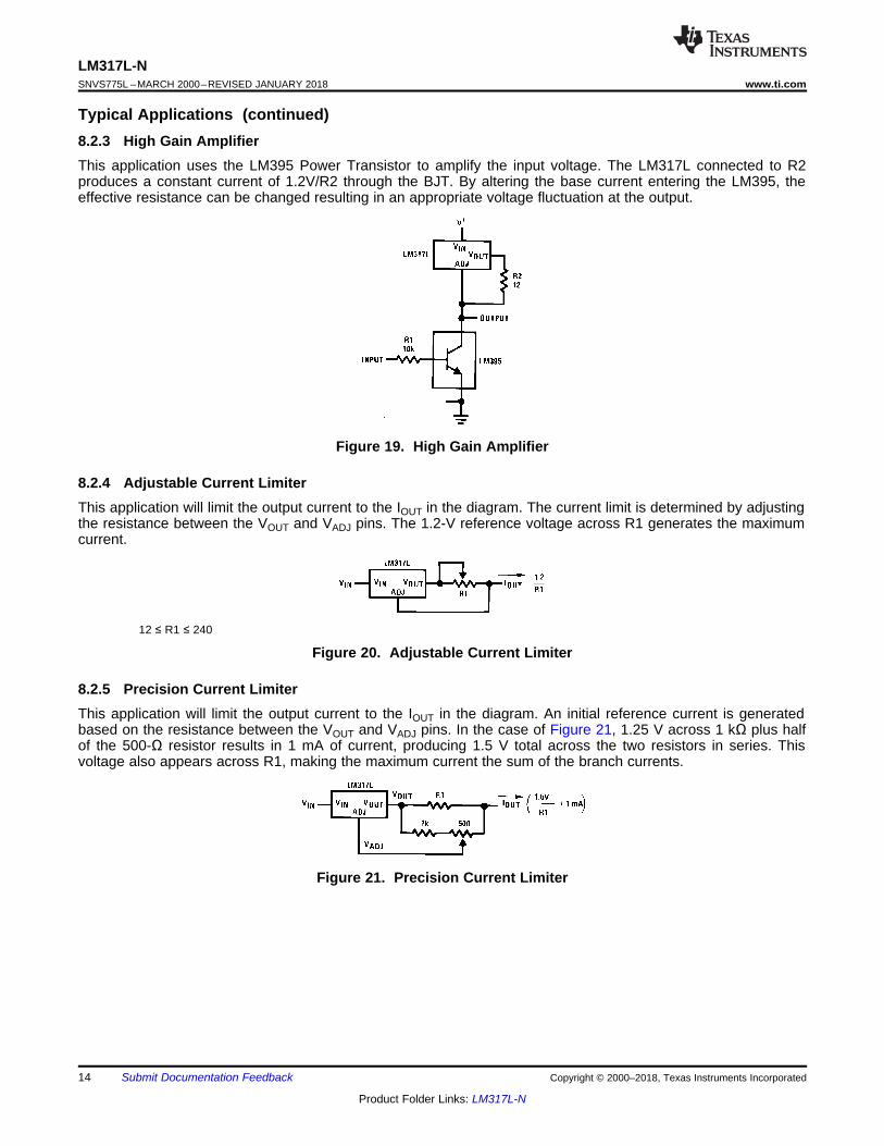
8.2.2 Digitally-Selected OutputsFigure 18 demonstrates a digitally-selectable output voltage. In its default state, all transistors are off and theoutput voltage is set based on R1 and R2. By driving certain transistors, the associated resistor is connected inparallel to R2, modifying the output voltage of the regulator.
*Sets maximum VOUT
Figure 18. Digitally-Selected Outputs
14
LM317L-NSNVS775L –MARCH 2000–REVISED JANUARY 2018 www.ti.com
Product Folder Links: LM317L-N
Submit Documentation Feedback Copyright © 2000–2018, Texas Instruments Incorporated
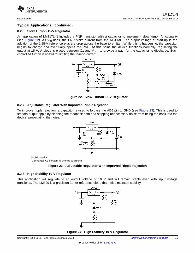
Typical Applications (continued)8.2.3 High Gain AmplifierThis application uses the LM395 Power Transistor to amplify the input voltage. The LM317L connected to R2produces a constant current of 1.2V/R2 through the BJT. By altering the base current entering the LM395, theeffective resistance can be changed resulting in an appropriate voltage fluctuation at the output.
Figure 19. High Gain Amplifier
8.2.4 Adjustable Current LimiterThis application will limit the output current to the IOUT in the diagram. The current limit is determined by adjustingthe resistance between the VOUT and VADJ pins. The 1.2-V reference voltage across R1 generates the maximumcurrent.
12 ≤ R1 ≤ 240
Figure 20. Adjustable Current Limiter
8.2.5 Precision Current LimiterThis application will limit the output current to the IOUT in the diagram. An initial reference current is generatedbased on the resistance between the VOUT and VADJ pins. In the case of Figure 21, 1.25 V across 1 kΩ plus halfof the 500-Ω resistor results in 1 mA of current, producing 1.5 V total across the two resistors in series. Thisvoltage also appears across R1, making the maximum current the sum of the branch currents.
Figure 21. Precision Current Limiter
15
LM317L-Nwww.ti.com SNVS775L –MARCH 2000–REVISED JANUARY 2018
Product Folder Links: LM317L-N
Submit Documentation FeedbackCopyright © 2000–2018, Texas Instruments Incorporated
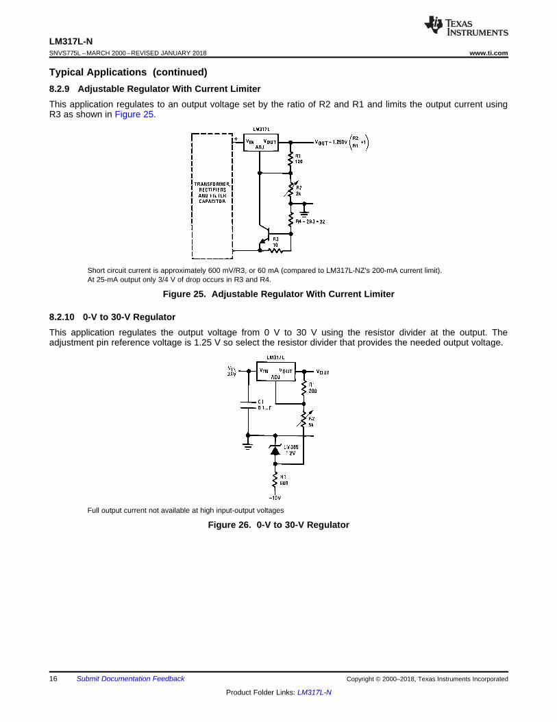
Typical Applications (continued)8.2.6 Slow Turnon 15-V RegulatorAn application of LM317L-N includes a PNP transistor with a capacitor to implement slow turnon functionality(see Figure 22). As VIN rises, the PNP sinks current from the ADJ rail. The output voltage at start-up is theaddition of the 1.25-V reference plus the drop across the base to emitter. While this is happening, the capacitorbegins to charge and eventually opens the PNP. At this point, the device functions normally, regulating theoutput at 15 V. A diode is placed between C1 and VOUT to provide a path for the capacitor to discharge. Suchcontrolled turnon is useful for limiting the in-rush current.
Figure 22. Slow Turnon 15-V Regulator
8.2.7 Adjustable Regulator With Improved Ripple RejectionTo improve ripple rejection, a capacitor is used to bypass the ADJ pin to GND (see Figure 23). This is used tosmooth output ripple by cleaning the feedback path and stopping unnecessary noise from being fed back into thedevice, propagating the noise.
†Solid tantalum*Discharges C1 if output is shorted to ground
Figure 23. Adjustable Regulator With Improved Ripple Rejection
8.2.8 High Stability 10-V RegulatorThis application will regulate to an output voltage of 10 V and will remain stable even with input voltagetransients. The LM329 is a precision Zener reference diode that helps maintain stability.
Figure 24. High Stability 10-V Regulator
16
LM317L-NSNVS775L –MARCH 2000–REVISED JANUARY 2018 www.ti.com
Product Folder Links: LM317L-N
Submit Documentation Feedback Copyright © 2000–2018, Texas Instruments Incorporated
Typical Applications (continued)8.2.9 Adjustable Regulator With Current LimiterThis application regulates to an output voltage set by the ratio of R2 and R1 and limits the output current usingR3 as shown in Figure 25.
Short circuit current is approximately 600 mV/R3, or 60 mA (compared to LM317L-NZ's 200-mA current limit).At 25-mA output only 3/4 V of drop occurs in R3 and R4.
Figure 25. Adjustable Regulator With Current Limiter
8.2.10 0-V to 30-V RegulatorThis application regulates the output voltage from 0 V to 30 V using the resistor divider at the output. Theadjustment pin reference voltage is 1.25 V so select the resistor divider that provides the needed output voltage.
Full output current not available at high input-output voltages
Figure 26. 0-V to 30-V Regulator
17
LM317L-Nwww.ti.com SNVS775L –MARCH 2000–REVISED JANUARY 2018
Product Folder Links: LM317L-N
Submit Documentation FeedbackCopyright © 2000–2018, Texas Instruments Incorporated
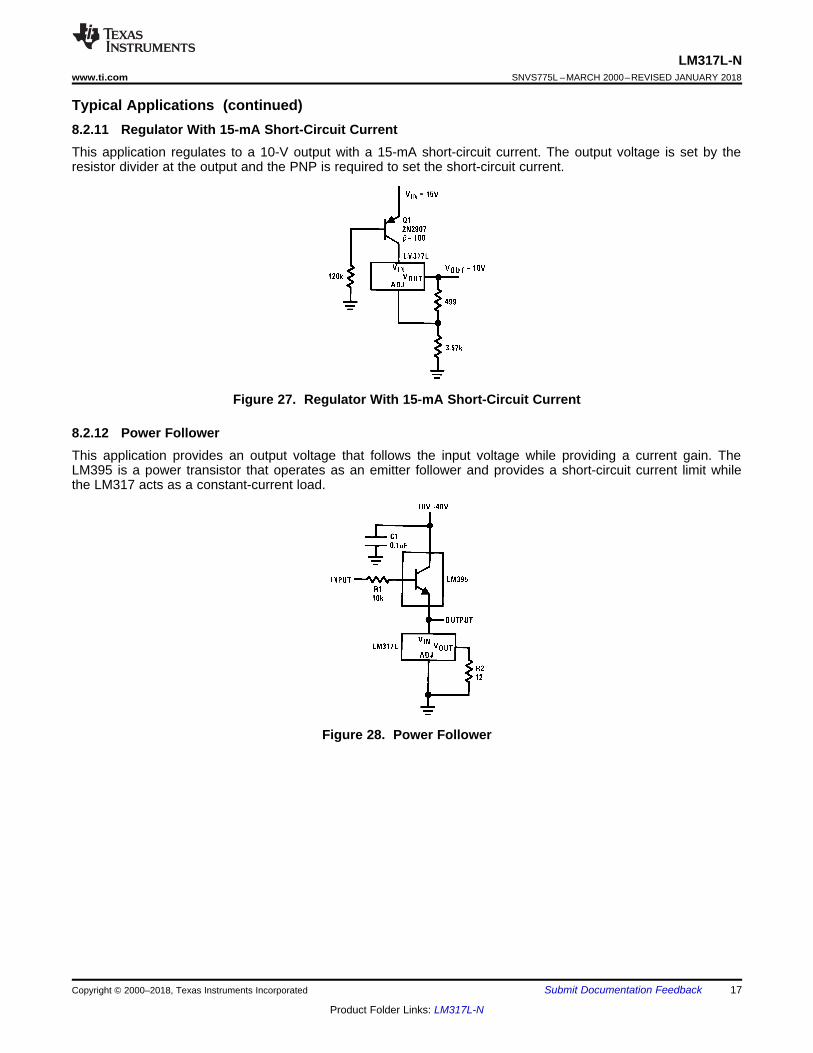
Typical Applications (continued)8.2.11 Regulator With 15-mA Short-Circuit CurrentThis application regulates to a 10-V output with a 15-mA short-circuit current. The output voltage is set by theresistor divider at the output and the PNP is required to set the short-circuit current.
Figure 27. Regulator With 15-mA Short-Circuit Current
8.2.12 Power FollowerThis application provides an output voltage that follows the input voltage while providing a current gain. TheLM395 is a power transistor that operates as an emitter follower and provides a short-circuit current limit whilethe LM317 acts as a constant-current load.
Figure 28. Power Follower
18
LM317L-NSNVS775L –MARCH 2000–REVISED JANUARY 2018 www.ti.com
Product Folder Links: LM317L-N
Submit Documentation Feedback Copyright © 2000–2018, Texas Instruments Incorporated
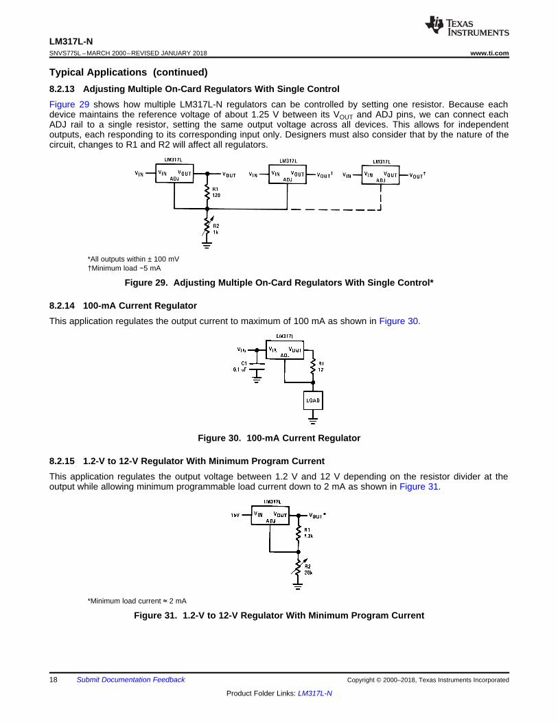
Typical Applications (continued)8.2.13 Adjusting Multiple On-Card Regulators With Single ControlFigure 29 shows how multiple LM317L-N regulators can be controlled by setting one resistor. Because eachdevice maintains the reference voltage of about 1.25 V between its VOUT and ADJ pins, we can connect eachADJ rail to a single resistor, setting the same output voltage across all devices. This allows for independentoutputs, each responding to its corresponding input only. Designers must also consider that by the nature of thecircuit, changes to R1 and R2 will affect all regulators.
*All outputs within ± 100 mV†Minimum load −5 mA
Figure 29. Adjusting Multiple On-Card Regulators With Single Control*
8.2.14 100-mA Current RegulatorThis application regulates the output current to maximum of 100 mA as shown in Figure 30.
Figure 30. 100-mA Current Regulator
8.2.15 1.2-V to 12-V Regulator With Minimum Program CurrentThis application regulates the output voltage between 1.2 V and 12 V depending on the resistor divider at theoutput while allowing minimum programmable load current down to 2 mA as shown in Figure 31.
*Minimum load current ≈ 2 mA
Figure 31. 1.2-V to 12-V Regulator With Minimum Program Current
19
LM317L-Nwww.ti.com SNVS775L –MARCH 2000–REVISED JANUARY 2018
Product Folder Links: LM317L-N
Submit Documentation FeedbackCopyright © 2000–2018, Texas Instruments Incorporated
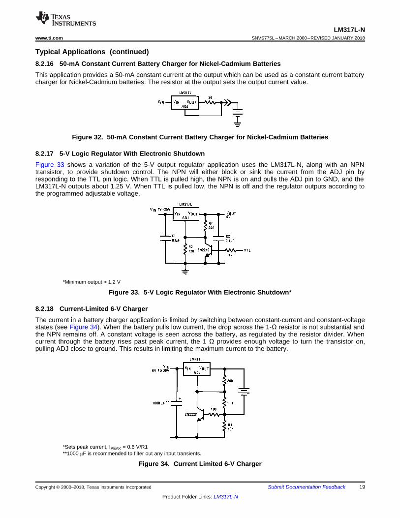
Typical Applications (continued)8.2.16 50-mA Constant Current Battery Charger for Nickel-Cadmium BatteriesThis application provides a 50-mA constant current at the output which can be used as a constant current batterycharger for Nickel-Cadmium batteries. The resistor at the output sets the output current value.
Figure 32. 50-mA Constant Current Battery Charger for Nickel-Cadmium Batteries
8.2.17 5-V Logic Regulator With Electronic ShutdownFigure 33 shows a variation of the 5-V output regulator application uses the LM317L-N, along with an NPNtransistor, to provide shutdown control. The NPN will either block or sink the current from the ADJ pin byresponding to the TTL pin logic. When TTL is pulled high, the NPN is on and pulls the ADJ pin to GND, and theLM317L-N outputs about 1.25 V. When TTL is pulled low, the NPN is off and the regulator outputs according tothe programmed adjustable voltage.
*Minimum output ≈ 1.2 V
Figure 33. 5-V Logic Regulator With Electronic Shutdown*
8.2.18 Current-Limited 6-V ChargerThe current in a battery charger application is limited by switching between constant-current and constant-voltagestates (see Figure 34). When the battery pulls low current, the drop across the 1-Ω resistor is not substantial andthe NPN remains off. A constant voltage is seen across the battery, as regulated by the resistor divider. Whencurrent through the battery rises past peak current, the 1 Ω provides enough voltage to turn the transistor on,pulling ADJ close to ground. This results in limiting the maximum current to the battery.
*Sets peak current, IPEAK = 0.6 V/R1**1000 μF is recommended to filter out any input transients.
Figure 34. Current Limited 6-V Charger
20
LM317L-NSNVS775L –MARCH 2000–REVISED JANUARY 2018 www.ti.com
Product Folder Links: LM317L-N
Submit Documentation Feedback Copyright © 2000–2018, Texas Instruments Incorporated
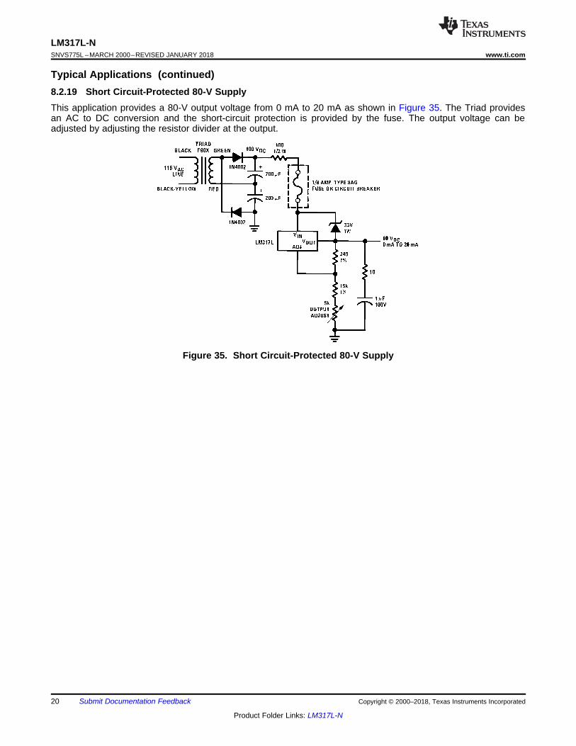
Typical Applications (continued)8.2.19 Short Circuit-Protected 80-V SupplyThis application provides a 80-V output voltage from 0 mA to 20 mA as shown in Figure 35. The Triad providesan AC to DC conversion and the short-circuit protection is provided by the fuse. The output voltage can beadjusted by adjusting the resistor divider at the output.
Figure 35. Short Circuit-Protected 80-V Supply
21
LM317L-Nwww.ti.com SNVS775L –MARCH 2000–REVISED JANUARY 2018
Product Folder Links: LM317L-N
Submit Documentation FeedbackCopyright © 2000–2018, Texas Instruments Incorporated
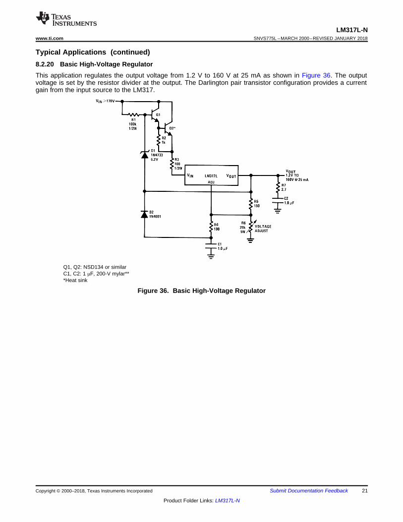
Typical Applications (continued)8.2.20 Basic High-Voltage RegulatorThis application regulates the output voltage from 1.2 V to 160 V at 25 mA as shown in Figure 36. The outputvoltage is set by the resistor divider at the output. The Darlington pair transistor configuration provides a currentgain from the input source to the LM317.
Q1, Q2: NSD134 or similarC1, C2: 1 μF, 200-V mylar***Heat sink
Figure 36. Basic High-Voltage Regulator
22
LM317L-NSNVS775L –MARCH 2000–REVISED JANUARY 2018 www.ti.com
Product Folder Links: LM317L-N
Submit Documentation Feedback Copyright © 2000–2018, Texas Instruments Incorporated
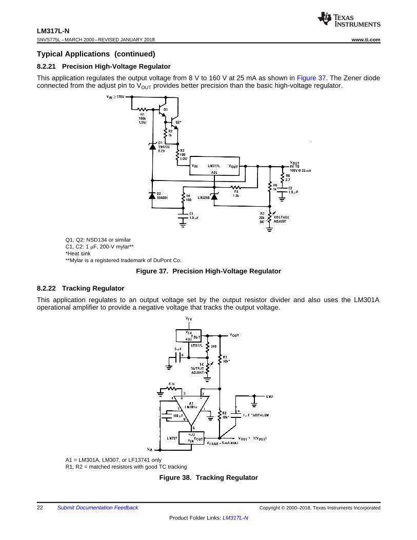
Typical Applications (continued)8.2.21 Precision High-Voltage RegulatorThis application regulates the output voltage from 8 V to 160 V at 25 mA as shown in Figure 37. The Zener diodeconnected from the adjust pin to VOUT provides better precision than the basic high-voltage regulator.
Q1, Q2: NSD134 or similarC1, C2: 1 μF, 200-V mylar***Heat sink**Mylar is a registered trademark of DuPont Co.
Figure 37. Precision High-Voltage Regulator
8.2.22 Tracking RegulatorThis application regulates to an output voltage set by the output resistor divider and also uses the LM301Aoperational amplifier to provide a negative voltage that tracks the output voltage.
A1 = LM301A, LM307, or LF13741 onlyR1, R2 = matched resistors with good TC tracking
Figure 38. Tracking Regulator
23
LM317L-Nwww.ti.com SNVS775L –MARCH 2000–REVISED JANUARY 2018
Product Folder Links: LM317L-N
Submit Documentation FeedbackCopyright © 2000–2018, Texas Instruments Incorporated
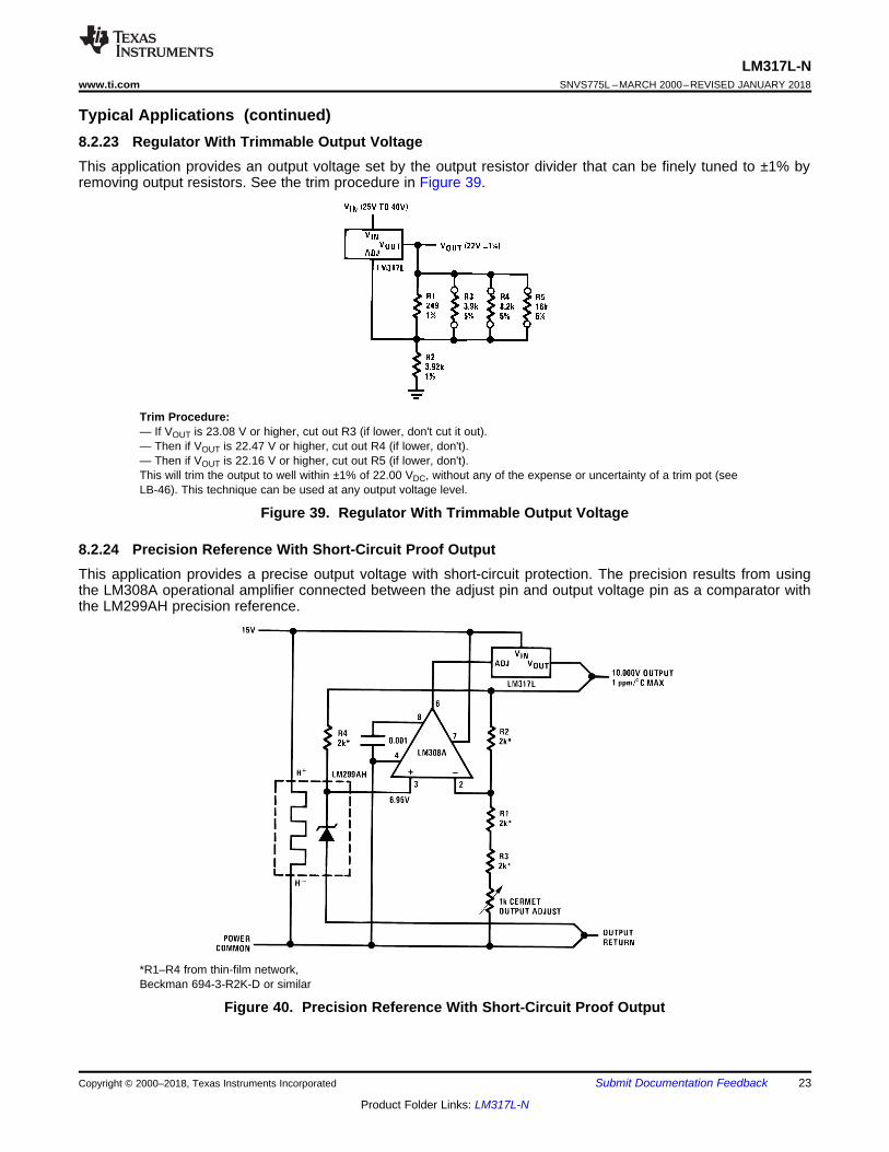
Typical Applications (continued)8.2.23 Regulator With Trimmable Output VoltageThis application provides an output voltage set by the output resistor divider that can be finely tuned to ±1% byremoving output resistors. See the trim procedure in Figure 39.
Trim Procedure:— If VOUT is 23.08 V or higher, cut out R3 (if lower, don't cut it out).— Then if VOUT is 22.47 V or higher, cut out R4 (if lower, don't).— Then if VOUT is 22.16 V or higher, cut out R5 (if lower, don't).This will trim the output to well within ±1% of 22.00 VDC, without any of the expense or uncertainty of a trim pot (seeLB-46). This technique can be used at any output voltage level.
Figure 39. Regulator With Trimmable Output Voltage
8.2.24 Precision Reference With Short-Circuit Proof OutputThis application provides a precise output voltage with short-circuit protection. The precision results from usingthe LM308A operational amplifier connected between the adjust pin and output voltage pin as a comparator withthe LM299AH precision reference.
*R1–R4 from thin-film network,Beckman 694-3-R2K-D or similar
Figure 40. Precision Reference With Short-Circuit Proof Output
24
LM317L-NSNVS775L –MARCH 2000–REVISED JANUARY 2018 www.ti.com
Product Folder Links: LM317L-N
Submit Documentation Feedback Copyright © 2000–2018, Texas Instruments Incorporated
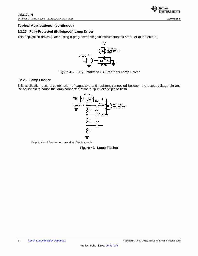
Typical Applications (continued)8.2.25 Fully-Protected (Bulletproof) Lamp DriverThis application drives a lamp using a programmable gain instrumentation amplifier at the output.
Figure 41. Fully-Protected (Bulletproof) Lamp Driver
8.2.26 Lamp FlasherThis application uses a combination of capacitors and resistors connected between the output voltage pin andthe adjust pin to cause the lamp connected at the output voltage pin to flash.
Output rate—4 flashes per second at 10% duty cycle
Figure 42. Lamp Flasher
25
LM317L-Nwww.ti.com SNVS775L –MARCH 2000–REVISED JANUARY 2018
Product Folder Links: LM317L-N
Submit Documentation FeedbackCopyright © 2000–2018, Texas Instruments Incorporated
9 Power Supply RecommendationsThe input supply to the LM317L-N must be kept at a voltage level lower than the maximum input-to-outputdifferential voltage of 40 V. When possible, the minimum dropout voltage must also be met with extra headroomto keep the LM317L-N in regulation. TI recommends using an input capacitor, especially when the input pin islocated more than 6 inches away from the power supply source. For more information regarding capacitorselection, see External Capacitors.
10 Layout
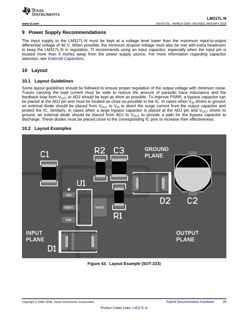
10.1 Layout GuidelinesSome layout guidelines should be followed to ensure proper regulation of the output voltage with minimum noise.Traces carrying the load current must be wide to reduce the amount of parasitic trace inductance and thefeedback loop from VOUT to ADJ should be kept as short as possible. To improve PSRR, a bypass capacitor canbe placed at the ADJ pin and must be located as close as possible to the IC. In cases when VIN shorts to ground,an external diode should be placed from VOUT to VIN to divert the surge current from the output capacitor andprotect the IC. Similarly, in cases when a large bypass capacitor is placed at the ADJ pin and VOUT shorts toground, an external diode should be placed from ADJ to VOUT to provide a path for the bypass capacitor todischarge. These diodes must be placed close to the corresponding IC pins to increase their effectiveness.
10.2 Layout Examples
Figure 43. Layout Example (SOT-223)
26
LM317L-NSNVS775L –MARCH 2000–REVISED JANUARY 2018 www.ti.com
Product Folder Links: LM317L-N
Submit Documentation Feedback Copyright © 2000–2018, Texas Instruments Incorporated
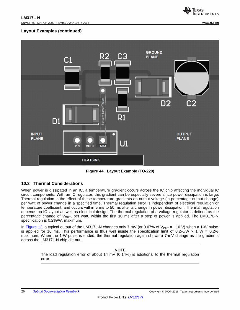
Layout Examples (continued)
Figure 44. Layout Example (TO-220)
10.3 Thermal ConsiderationsWhen power is dissipated in an IC, a temperature gradient occurs across the IC chip affecting the individual ICcircuit components. With an IC regulator, this gradient can be especially severe since power dissipation is large.Thermal regulation is the effect of these temperature gradients on output voltage (in percentage output change)per watt of power change in a specified time. Thermal regulation error is independent of electrical regulation ortemperature coefficient, and occurs within 5 ms to 50 ms after a change in power dissipation. Thermal regulationdepends on IC layout as well as electrical design. The thermal regulation of a voltage regulator is defined as thepercentage change of VOUT, per watt, within the first 10 ms after a step of power is applied. The LM317L-Nspecification is 0.2%/W, maximum.
In Figure 12, a typical output of the LM317L-N changes only 7 mV (or 0.07% of VOUT = −10 V) when a 1-W pulseis applied for 10 ms. This performance is thus well inside the specification limit of 0.2%/W × 1 W = 0.2%maximum. When the 1-W pulse is ended, the thermal regulation again shows a 7-mV change as the gradientsacross the LM317L-N chip die out.
NOTEThe load regulation error of about 14 mV (0.14%) is additional to the thermal regulationerror.
27
LM317L-Nwww.ti.com SNVS775L –MARCH 2000–REVISED JANUARY 2018
Product Folder Links: LM317L-N
Submit Documentation FeedbackCopyright © 2000–2018, Texas Instruments Incorporated
11 Device and Documentation Support
11.1 Documentation Support
11.1.1 Related DocumentationFor related documentation, see the following:
AN-1112 DSBGA Wafer Level Chip Scale Package (SNVA009)
11.2 Community ResourcesThe following links connect to TI community resources. Linked contents are provided "AS IS" by the respectivecontributors. They do not constitute TI specifications and do not necessarily reflect TI's views; see TI's Terms ofUse.
TI E2E™ Online Community TI's Engineer-to-Engineer (E2E) Community. Created to foster collaborationamong engineers. At e2e.ti.com, you can ask questions, share knowledge, explore ideas and helpsolve problems with fellow engineers.
Design Support TI's Design Support Quickly find helpful E2E forums along with design support tools andcontact information for technical support.
11.3 TrademarksE2E is a trademark of Texas Instruments.All other trademarks are the property of their respective owners.
11.4 Electrostatic Discharge CautionThese devices have limited built-in ESD protection. The leads should be shorted together or the device placed in conductive foamduring storage or handling to prevent electrostatic damage to the MOS gates.
11.5 GlossarySLYZ022 — TI Glossary.
This glossary lists and explains terms, acronyms, and definitions.
12 Mechanical, Packaging, and Orderable InformationThe following pages include mechanical, packaging, and orderable information. This information is the mostcurrent data available for the designated devices. This data is subject to change without notice and revision ofthis document. For browser-based versions of this data sheet, refer to the left-hand navigation.
PACKAGE OPTION ADDENDUM
www.ti.com 31-Jan-2017
Addendum-Page 1
PACKAGING INFORMATION
Orderable Device Status(1)
Package Type PackageDrawing
Pins PackageQty
Eco Plan(2)
Lead/Ball Finish(6)
MSL Peak Temp(3)
Op Temp (°C) Device Marking(4/5)
Samples
LM317LITP/NOPB ACTIVE DSBGA YPB 6 250 Green (RoHS& no Sb/Br)
SNAGCU Level-1-260C-UNLIM -40 to 125 P1
LM317LITPX/NOPB ACTIVE DSBGA YPB 6 3000 Green (RoHS& no Sb/Br)
SNAGCU Level-1-260C-UNLIM -40 to 125 P1
LM317LM/NOPB ACTIVE SOIC D 8 95 Green (RoHS& no Sb/Br)
CU SN Level-1-260C-UNLIM -40 to 125 LM317LM
LM317LMX NRND SOIC D 8 2500 TBD Call TI Call TI -40 to 125 LM317LM
LM317LMX/NOPB ACTIVE SOIC D 8 2500 Green (RoHS& no Sb/Br)
CU SN Level-1-260C-UNLIM -40 to 125 LM317LM
LM317LZ/LFT1 ACTIVE TO-92 LP 3 2000 Green (RoHS& no Sb/Br)
CU SN N / A for Pkg Type LM317LZ
LM317LZ/LFT2 ACTIVE TO-92 LP 3 2000 Green (RoHS& no Sb/Br)
CU SN N / A for Pkg Type LM317LZ
LM317LZ/LFT3 ACTIVE TO-92 LP 3 2000 Green (RoHS& no Sb/Br)
CU SN N / A for Pkg Type LM317LZ
LM317LZ/LFT4 ACTIVE TO-92 LP 3 2000 Green (RoHS& no Sb/Br)
CU SN N / A for Pkg Type LM317LZ
LM317LZ/LFT7 ACTIVE TO-92 LP 3 2000 Green (RoHS& no Sb/Br)
CU SN N / A for Pkg Type LM317LZ
LM317LZ/NOPB ACTIVE TO-92 LP 3 1800 Green (RoHS& no Sb/Br)
CU SN N / A for Pkg Type -40 to 125 LM317LZ
(1) The marketing status values are defined as follows:ACTIVE: Product device recommended for new designs.LIFEBUY: TI has announced that the device will be discontinued, and a lifetime-buy period is in effect.NRND: Not recommended for new designs. Device is in production to support existing customers, but TI does not recommend using this part in a new design.PREVIEW: Device has been announced but is not in production. Samples may or may not be available.OBSOLETE: TI has discontinued the production of the device.
(2) Eco Plan - The planned eco-friendly classification: Pb-Free (RoHS), Pb-Free (RoHS Exempt), or Green (RoHS & no Sb/Br) - please check http://www.ti.com/productcontent for the latest availabilityinformation and additional product content details.TBD: The Pb-Free/Green conversion plan has not been defined.Pb-Free (RoHS): TI's terms "Lead-Free" or "Pb-Free" mean semiconductor products that are compatible with the current RoHS requirements for all 6 substances, including the requirement thatlead not exceed 0.1% by weight in homogeneous materials. Where designed to be soldered at high temperatures, TI Pb-Free products are suitable for use in specified lead-free processes.
PACKAGE OPTION ADDENDUM
www.ti.com 31-Jan-2017
Addendum-Page 2
Pb-Free (RoHS Exempt): This component has a RoHS exemption for either 1) lead-based flip-chip solder bumps used between the die and package, or 2) lead-based die adhesive used betweenthe die and leadframe. The component is otherwise considered Pb-Free (RoHS compatible) as defined above.Green (RoHS & no Sb/Br): TI defines "Green" to mean Pb-Free (RoHS compatible), and free of Bromine (Br) and Antimony (Sb) based flame retardants (Br or Sb do not exceed 0.1% by weightin homogeneous material)
(3) MSL, Peak Temp. - The Moisture Sensitivity Level rating according to the JEDEC industry standard classifications, and peak solder temperature.
(4) There may be additional marking, which relates to the logo, the lot trace code information, or the environmental category on the device.
(5) Multiple Device Markings will be inside parentheses. Only one Device Marking contained in parentheses and separated by a "~" will appear on a device. If a line is indented then it is a continuationof the previous line and the two combined represent the entire Device Marking for that device.
(6) Lead/Ball Finish - Orderable Devices may have multiple material finish options. Finish options are separated by a vertical ruled line. Lead/Ball Finish values may wrap to two lines if the finishvalue exceeds the maximum column width.
Important Information and Disclaimer:The information provided on this page represents TI's knowledge and belief as of the date that it is provided. TI bases its knowledge and belief on informationprovided by third parties, and makes no representation or warranty as to the accuracy of such information. Efforts are underway to better integrate information from third parties. TI has taken andcontinues to take reasonable steps to provide representative and accurate information but may not have conducted destructive testing or chemical analysis on incoming materials and chemicals.TI and TI suppliers consider certain information to be proprietary, and thus CAS numbers and other limited information may not be available for release.
In no event shall TI's liability arising out of such information exceed the total purchase price of the TI part(s) at issue in this document sold by TI to Customer on an annual basis.
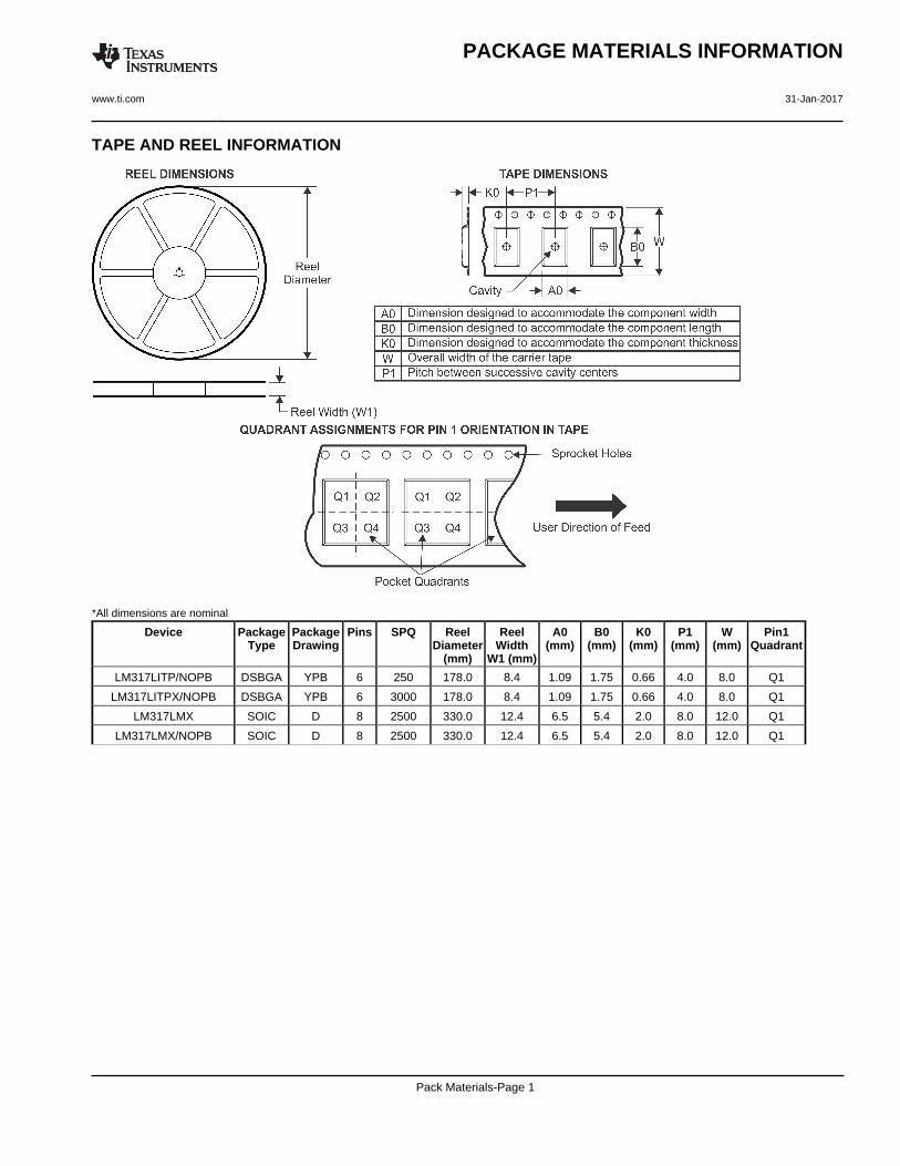
TAPE AND REEL INFORMATION
*All dimensions are nominal
Device PackageType
PackageDrawing
Pins SPQ ReelDiameter
(mm)
ReelWidth
W1 (mm)
A0(mm)
B0(mm)
K0(mm)
P1(mm)
W(mm)
Pin1Quadrant
LM317LITP/NOPB DSBGA YPB 6 250 178.0 8.4 1.09 1.75 0.66 4.0 8.0 Q1
LM317LITPX/NOPB DSBGA YPB 6 3000 178.0 8.4 1.09 1.75 0.66 4.0 8.0 Q1
LM317LMX SOIC D 8 2500 330.0 12.4 6.5 5.4 2.0 8.0 12.0 Q1
LM317LMX/NOPB SOIC D 8 2500 330.0 12.4 6.5 5.4 2.0 8.0 12.0 Q1
PACKAGE MATERIALS INFORMATION
www.ti.com 31-Jan-2017
Pack Materials-Page 1
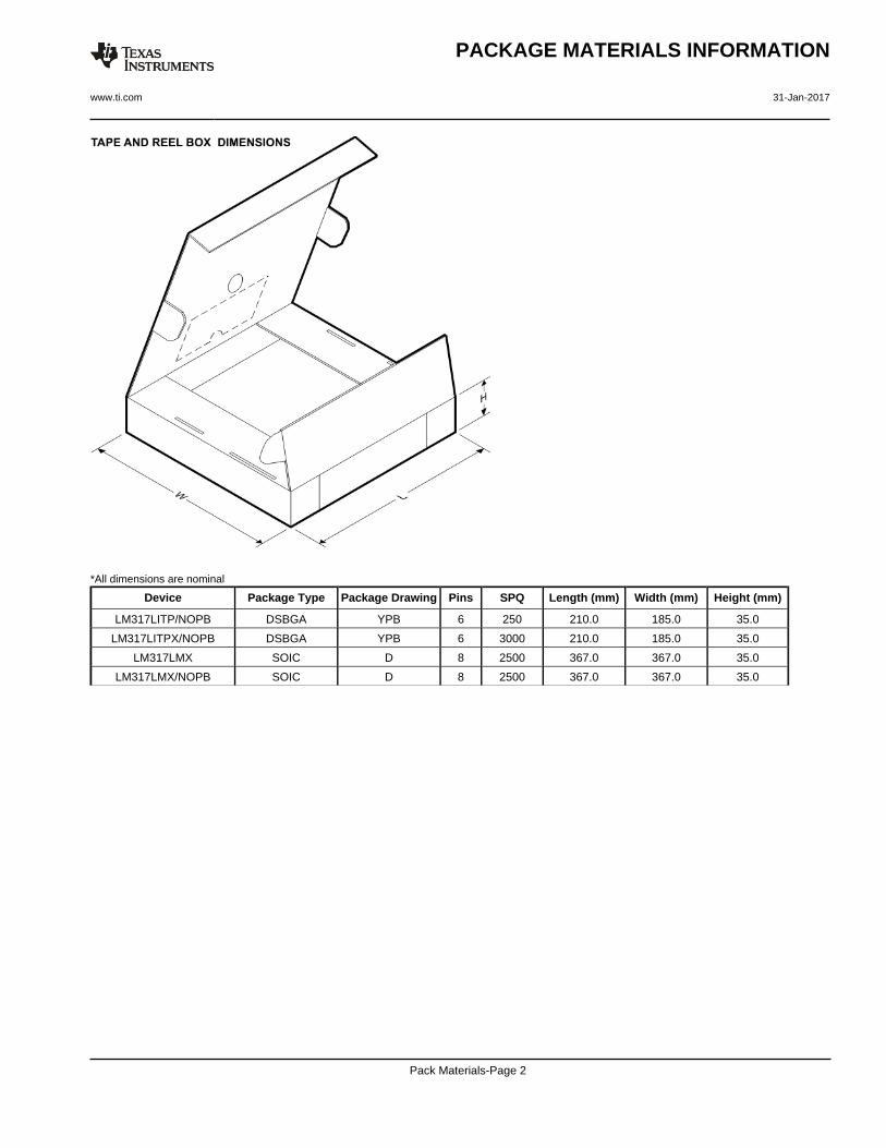
*All dimensions are nominal
Device Package Type Package Drawing Pins SPQ Length (mm) Width (mm) Height (mm)
LM317LITP/NOPB DSBGA YPB 6 250 210.0 185.0 35.0
LM317LITPX/NOPB DSBGA YPB 6 3000 210.0 185.0 35.0
LM317LMX SOIC D 8 2500 367.0 367.0 35.0
LM317LMX/NOPB SOIC D 8 2500 367.0 367.0 35.0
PACKAGE MATERIALS INFORMATION
www.ti.com 31-Jan-2017
Pack Materials-Page 2
IMPORTANT NOTICE
Texas Instruments Incorporated (TI) reserves the right to make corrections, enhancements, improvements and other changes to itssemiconductor products and services per JESD46, latest issue, and to discontinue any product or service per JESD48, latest issue. Buyersshould obtain the latest relevant information before placing orders and should verify that such information is current and complete.TI’s published terms of sale for semiconductor products (http://www.ti.com/sc/docs/stdterms.htm) apply to the sale of packaged integratedcircuit products that TI has qualified and released to market. Additional terms may apply to the use or sale of other types of TI products andservices.Reproduction of significant portions of TI information in TI data sheets is permissible only if reproduction is without alteration and isaccompanied by all associated warranties, conditions, limitations, and notices. TI is not responsible or liable for such reproduceddocumentation. Information of third parties may be subject to additional restrictions. Resale of TI products or services with statementsdifferent from or beyond the parameters stated by TI for that product or service voids all express and any implied warranties for theassociated TI product or service and is an unfair and deceptive business practice. TI is not responsible or liable for any such statements.Buyers and others who are developing systems that incorporate TI products (collectively, “Designers”) understand and agree that Designersremain responsible for using their independent analysis, evaluation and judgment in designing their applications and that Designers havefull and exclusive responsibility to assure the safety of Designers' applications and compliance of their applications (and of all TI productsused in or for Designers’ applications) with all applicable regulations, laws and other applicable requirements. Designer represents that, withrespect to their applications, Designer has all the necessary expertise to create and implement safeguards that (1) anticipate dangerousconsequences of failures, (2) monitor failures and their consequences, and (3) lessen the likelihood of failures that might cause harm andtake appropriate actions. Designer agrees that prior to using or distributing any applications that include TI products, Designer willthoroughly test such applications and the functionality of such TI products as used in such applications.TI’s provision of technical, application or other design advice, quality characterization, reliability data or other services or information,including, but not limited to, reference designs and materials relating to evaluation modules, (collectively, “TI Resources”) are intended toassist designers who are developing applications that incorporate TI products; by downloading, accessing or using TI Resources in anyway, Designer (individually or, if Designer is acting on behalf of a company, Designer’s company) agrees to use any particular TI Resourcesolely for this purpose and subject to the terms of this Notice.TI’s provision of TI Resources does not expand or otherwise alter TI’s applicable published warranties or warranty disclaimers for TIproducts, and no additional obligations or liabilities arise from TI providing such TI Resources. TI reserves the right to make corrections,enhancements, improvements and other changes to its TI Resources. TI has not conducted any testing other than that specificallydescribed in the published documentation for a particular TI Resource.Designer is authorized to use, copy and modify any individual TI Resource only in connection with the development of applications thatinclude the TI product(s) identified in such TI Resource. NO OTHER LICENSE, EXPRESS OR IMPLIED, BY ESTOPPEL OR OTHERWISETO ANY OTHER TI INTELLECTUAL PROPERTY RIGHT, AND NO LICENSE TO ANY TECHNOLOGY OR INTELLECTUAL PROPERTYRIGHT OF TI OR ANY THIRD PARTY IS GRANTED HEREIN, including but not limited to any patent right, copyright, mask work right, orother intellectual property right relating to any combination, machine, or process in which TI products or services are used. Informationregarding or referencing third-party products or services does not constitute a license to use such products or services, or a warranty orendorsement thereof. Use of TI Resources may require a license from a third party under the patents or other intellectual property of thethird party, or a license from TI under the patents or other intellectual property of TI.TI RESOURCES ARE PROVIDED “AS IS” AND WITH ALL FAULTS. TI DISCLAIMS ALL OTHER WARRANTIES ORREPRESENTATIONS, EXPRESS OR IMPLIED, REGARDING RESOURCES OR USE THEREOF, INCLUDING BUT NOT LIMITED TOACCURACY OR COMPLETENESS, TITLE, ANY EPIDEMIC FAILURE WARRANTY AND ANY IMPLIED WARRANTIES OFMERCHANTABILITY, FITNESS FOR A PARTICULAR PURPOSE, AND NON-INFRINGEMENT OF ANY THIRD PARTY INTELLECTUALPROPERTY RIGHTS. TI SHALL NOT BE LIABLE FOR AND SHALL NOT DEFEND OR INDEMNIFY DESIGNER AGAINST ANY CLAIM,INCLUDING BUT NOT LIMITED TO ANY INFRINGEMENT CLAIM THAT RELATES TO OR IS BASED ON ANY COMBINATION OFPRODUCTS EVEN IF DESCRIBED IN TI RESOURCES OR OTHERWISE. IN NO EVENT SHALL TI BE LIABLE FOR ANY ACTUAL,DIRECT, SPECIAL, COLLATERAL, INDIRECT, PUNITIVE, INCIDENTAL, CONSEQUENTIAL OR EXEMPLARY DAMAGES INCONNECTION WITH OR ARISING OUT OF TI RESOURCES OR USE THEREOF, AND REGARDLESS OF WHETHER TI HAS BEENADVISED OF THE POSSIBILITY OF SUCH DAMAGES.Unless TI has explicitly designated an individual product as meeting the requirements of a particular industry standard (e.g., ISO/TS 16949and ISO 26262), TI is not responsible for any failure to meet such industry standard requirements.Where TI specifically promotes products as facilitating functional safety or as compliant with industry functional safety standards, suchproducts are intended to help enable customers to design and create their own applications that meet applicable functional safety standardsand requirements. Using products in an application does not by itself establish any safety features in the application. Designers mustensure compliance with safety-related requirements and standards applicable to their applications. Designer may not use any TI products inlife-critical medical equipment unless authorized officers of the parties have executed a special contract specifically governing such use.Life-critical medical equipment is medical equipment where failure of such equipment would cause serious bodily injury or death (e.g., lifesupport, pacemakers, defibrillators, heart pumps, neurostimulators, and implantables). Such equipment includes, without limitation, allmedical devices identified by the U.S. Food and Drug Administration as Class III devices and equivalent classifications outside the U.S.TI may expressly designate certain products as completing a particular qualification (e.g., Q100, Military Grade, or Enhanced Product).Designers agree that it has the necessary expertise to select the product with the appropriate qualification designation for their applicationsand that proper product selection is at Designers’ own risk. Designers are solely responsible for compliance with all legal and regulatoryrequirements in connection with such selection.Designer will fully indemnify TI and its representatives against any damages, costs, losses, and/or liabilities arising out of Designer’s non-compliance with the terms and provisions of this Notice.
Mailing Address: Texas Instruments, Post Office Box 655303, Dallas, Texas 75265Copyright © 2018, Texas Instruments Incorporated