Embed Size (px)
Citation preview
LM723, LM723C
www.ti.com SNVS765C –JUNE 1999–REVISED APRIL 2013
LM723/LM723C Voltage RegulatorCheck for Samples: LM723, LM723C
1FEATURES DESCRIPTIONThe LM723/LM723C is a voltage regulator designed
2• 150 mA Output Current Without External Passprimarily for series regulator applications. By itself, itTransistorwill supply output currents up to 150 mA; but external
• Output Currents in Excess of 10A Possible by transistors can be added to provide any desired loadAdding External Transistors current. The circuit features extremely low standby
current drain, and provision is made for either linear• Input Voltage 40V Maxor foldback current limiting.• Output Voltage Adjustable from 2V to 37VThe LM723/LM723C is also useful in a wide range of• Can be Used as Either a Linear or a Switchingother applications such as a shunt regulator, aRegulatorcurrent regulator or a temperature controller.
The LM723C is identical to the LM723 except that theLM723C has its performance ensured over a 0°C to+70°C temperature range, instead of −55°C to+125°C.
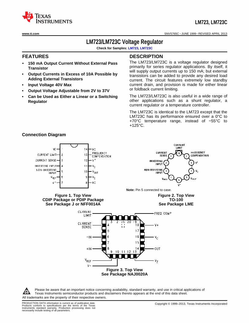
Connection Diagram
Note: Pin 5 connected to case.
Figure 1. Top View Figure 2. Top ViewCDIP Package or PDIP Package TO-100
See Package J or NFF0014A See Package LME
Figure 3. Top ViewSee Package NAJ0020A
1
Please be aware that an important notice concerning availability, standard warranty, and use in critical applications ofTexas Instruments semiconductor products and disclaimers thereto appears at the end of this data sheet.
2All trademarks are the property of their respective owners.
PRODUCTION DATA information is current as of publication date. Copyright © 1999–2013, Texas Instruments IncorporatedProducts conform to specifications per the terms of the TexasInstruments standard warranty. Production processing does notnecessarily include testing of all parameters.
LM723, LM723C
SNVS765C –JUNE 1999–REVISED APRIL 2013 www.ti.com
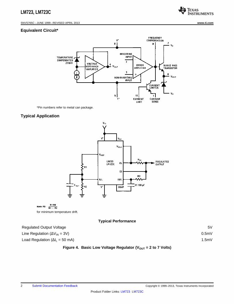
Equivalent Circuit*
*Pin numbers refer to metal can package.
Typical Application
for minimum temperature drift.
Typical Performance
Regulated Output Voltage 5V
Line Regulation (ΔVIN = 3V) 0.5mV
Load Regulation (ΔIL = 50 mA) 1.5mV
Figure 4. Basic Low Voltage Regulator (VOUT = 2 to 7 Volts)
2 Submit Documentation Feedback Copyright © 1999–2013, Texas Instruments Incorporated
Product Folder Links: LM723 LM723C
LM723, LM723C
www.ti.com SNVS765C –JUNE 1999–REVISED APRIL 2013
These devices have limited built-in ESD protection. The leads should be shorted together or the device placed in conductive foamduring storage or handling to prevent electrostatic damage to the MOS gates.
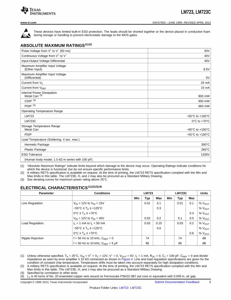
ABSOLUTE MAXIMUM RATINGS (1) (2)
Pulse Voltage from V+ to V− (50 ms) 50V
Continuous Voltage from V+ to V− 40V
Input-Output Voltage Differential 40V
Maximum Amplifier Input Voltage(Either Input) 8.5V
Maximum Amplifier Input Voltage(Differential) 5V
Current from VZ 25 mA
Current from VREF 15 mA
Internal Power DissipationMetal Can (3) 800 mW
CDIP (3) 900 mW
PDIP (3) 660 mW
Operating Temperature Range
LM723 −55°C to +150°C
LM723C 0°C to +70°C
Storage Temperature RangeMetal Can −65°C to +150°C
PDIP −55°C to +150°C
Lead Temperature (Soldering, 4 sec. max.)
Hermetic Package 300°C
Plastic Package 260°C
ESD Tolerance 1200V
(Human body model, 1.5 kΩ in series with 100 pF)
(1) “Absolute Maximum Ratings” indicate limits beyond which damage to the device may occur. Operating Ratings indicate conditions forwhich the device is functional, but do not ensure specific performance limits.
(2) A military RETS specification is available on request. At the time of printing, the LM723 RETS specification complied with the Min andMax limits in this table. The LM723E, H, and J may also be procured as a Standard Military Drawing.
(3) See derating curves for maximum power rating above 25°C.
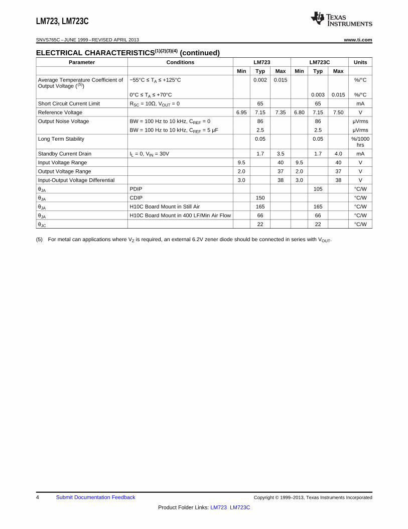
ELECTRICAL CHARACTERISTICS (1) (2) (3) (4)
Parameter Conditions LM723 LM723C Units
Min Typ Max Min Typ Max
Line Regulation VIN = 12V to VIN = 15V 0.01 0.1 0.01 0.1 % VOUT
−55°C ≤ TA ≤ +125°C 0.3 % VOUT
0°C ≤ TA ≤ +70°C 0.3 % VOUT
VIN = 12V to VIN = 40V 0.02 0.2 0.1 0.5 % VOUT
Load Regulation IL = 1 mA to IL = 50 mA 0.03 0.15 0.03 0.2 % VOUT
−55°C ≤ TA ≤ +125°C 0.6 % VOUT
0°C ≤ TA ≤ +70°C 0.6 % VOUT
Ripple Rejection f = 50 Hz to 10 kHz, CREF = 0 74 74 dB
f = 50 Hz to 10 kHz, CREF = 5 μF 86 86 dB
(1) Unless otherwise specified, TA = 25°C, VIN = V+ = VC = 12V, V− = 0, VOUT = 5V, IL = 1 mA, RSC = 0, C1 = 100 pF, CREF = 0 and dividerimpedance as seen by error amplifier ≤ 10 kΩ connected as shown in Figure 4. Line and load regulation specifications are given for thecondition of constant chip temperature. Temperature drifts must be taken into account separately for high dissipation conditions.
(2) A military RETS specification is available on request. At the time of printing, the LM723 RETS specification complied with the Min andMax limits in this table. The LM723E, H, and J may also be procured as a Standard Military Drawing.
(3) Specified by correlation to other tests.(4) L1 is 40 turns of No. 20 enameled copper wire wound on Ferroxcube P36/22-3B7 pot core or equivalent with 0.009 in. air gap.
Copyright © 1999–2013, Texas Instruments Incorporated Submit Documentation Feedback 3
Product Folder Links: LM723 LM723C
LM723, LM723C
SNVS765C –JUNE 1999–REVISED APRIL 2013 www.ti.com
ELECTRICAL CHARACTERISTICS(1)(2)(3)(4) (continued)Parameter Conditions LM723 LM723C Units
Min Typ Max Min Typ Max
Average Temperature Coefficient of −55°C ≤ TA ≤ +125°C 0.002 0.015 %/°COutput Voltage ( (5))
0°C ≤ TA ≤ +70°C 0.003 0.015 %/°C
Short Circuit Current Limit RSC = 10Ω, VOUT = 0 65 65 mA
Reference Voltage 6.95 7.15 7.35 6.80 7.15 7.50 V
Output Noise Voltage BW = 100 Hz to 10 kHz, CREF = 0 86 86 μVrms
BW = 100 Hz to 10 kHz, CREF = 5 μF 2.5 2.5 μVrms
Long Term Stability 0.05 0.05 %/1000hrs
Standby Current Drain IL = 0, VIN = 30V 1.7 3.5 1.7 4.0 mA
Input Voltage Range 9.5 40 9.5 40 V
Output Voltage Range 2.0 37 2.0 37 V
Input-Output Voltage Differential 3.0 38 3.0 38 V
θJA PDIP 105 °C/W
θJA CDIP 150 °C/W
θJA H10C Board Mount in Still Air 165 165 °C/W
θJA H10C Board Mount in 400 LF/Min Air Flow 66 66 °C/W
θJC 22 22 °C/W
(5) For metal can applications where VZ is required, an external 6.2V zener diode should be connected in series with VOUT.
4 Submit Documentation Feedback Copyright © 1999–2013, Texas Instruments Incorporated
Product Folder Links: LM723 LM723C
LM723, LM723C
www.ti.com SNVS765C –JUNE 1999–REVISED APRIL 2013
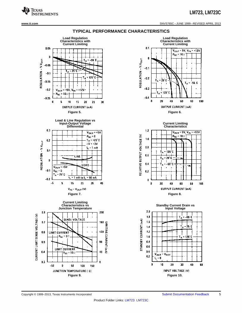
TYPICAL PERFORMANCE CHARACTERISTICS
Load Regulation Load RegulationCharacteristics with Characteristics with
Current Limiting Current Limiting
Figure 5. Figure 6.
Load & Line Regulation vsInput-Output Voltage Current Limiting
Differential Characteristics
Figure 7. Figure 8.
Current LimitingCharacteristics vs Standby Current Drain vs
Junction Temperature Input Voltage
Figure 9. Figure 10.
Copyright © 1999–2013, Texas Instruments Incorporated Submit Documentation Feedback 5
Product Folder Links: LM723 LM723C
LM723, LM723C
SNVS765C –JUNE 1999–REVISED APRIL 2013 www.ti.com
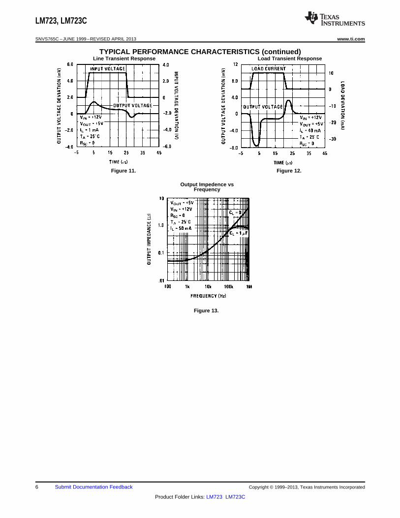
TYPICAL PERFORMANCE CHARACTERISTICS (continued)Line Transient Response Load Transient Response
Figure 11. Figure 12.
Output Impedence vsFrequency
Figure 13.
6 Submit Documentation Feedback Copyright © 1999–2013, Texas Instruments Incorporated
Product Folder Links: LM723 LM723C
LM723, LM723C
www.ti.com SNVS765C –JUNE 1999–REVISED APRIL 2013
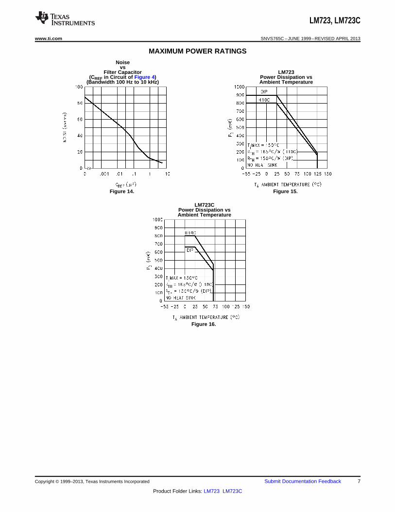
MAXIMUM POWER RATINGS
Noisevs
Filter Capacitor LM723(CREF in Circuit of Figure 4) Power Dissipation vs
(Bandwidth 100 Hz to 10 kHz) Ambient Temperature
Figure 14. Figure 15.
LM723CPower Dissipation vsAmbient Temperature
Figure 16.
Copyright © 1999–2013, Texas Instruments Incorporated Submit Documentation Feedback 7
Product Folder Links: LM723 LM723C
LM723, LM723C
SNVS765C –JUNE 1999–REVISED APRIL 2013 www.ti.com
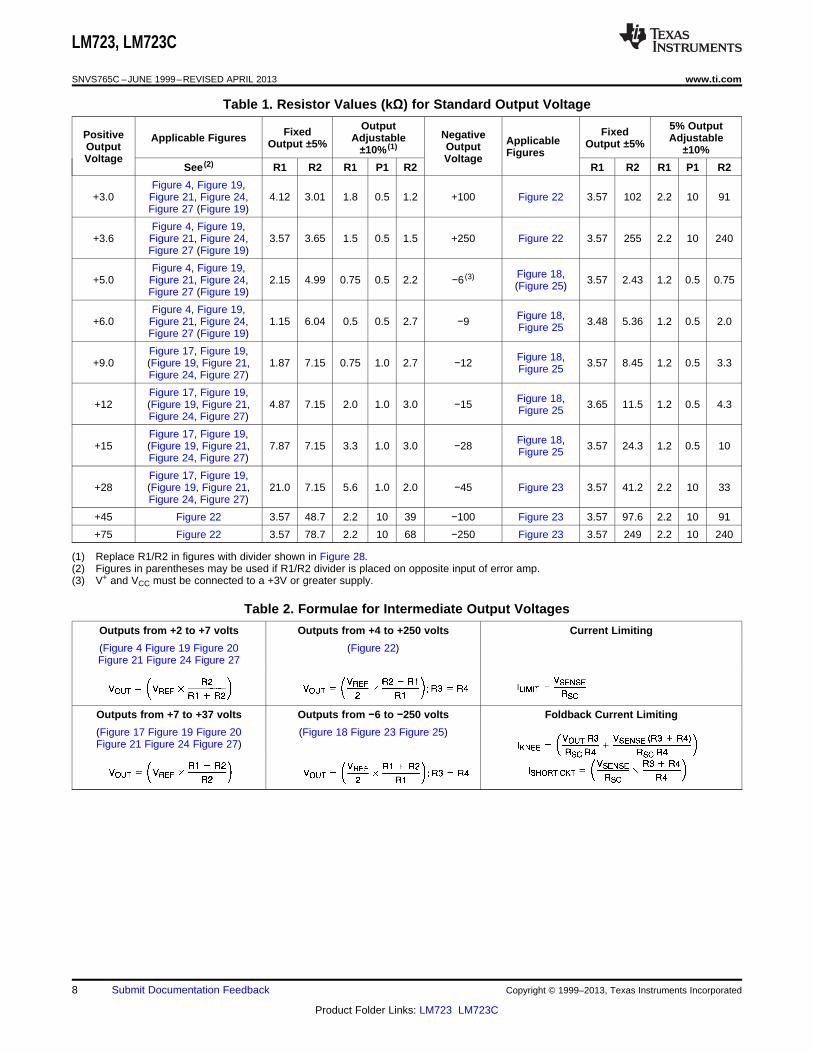
Table 1. Resistor Values (kΩ) for Standard Output Voltage
Output 5% OutputFixed FixedPositive NegativeApplicable Figures Adjustable AdjustableApplicableOutput ±5% Output ±5%Output Output±10% (1) ±10%FiguresVoltage VoltageSee (2) R1 R2 R1 P1 R2 R1 R2 R1 P1 R2
Figure 4, Figure 19,+3.0 Figure 21, Figure 24, 4.12 3.01 1.8 0.5 1.2 +100 Figure 22 3.57 102 2.2 10 91
Figure 27 (Figure 19)
Figure 4, Figure 19,+3.6 Figure 21, Figure 24, 3.57 3.65 1.5 0.5 1.5 +250 Figure 22 3.57 255 2.2 10 240
Figure 27 (Figure 19)
Figure 4, Figure 19, Figure 18,+5.0 Figure 21, Figure 24, 2.15 4.99 0.75 0.5 2.2 −6 (3) 3.57 2.43 1.2 0.5 0.75(Figure 25)Figure 27 (Figure 19)
Figure 4, Figure 19, Figure 18,+6.0 Figure 21, Figure 24, 1.15 6.04 0.5 0.5 2.7 −9 3.48 5.36 1.2 0.5 2.0Figure 25Figure 27 (Figure 19)
Figure 17, Figure 19, Figure 18,+9.0 (Figure 19, Figure 21, 1.87 7.15 0.75 1.0 2.7 −12 3.57 8.45 1.2 0.5 3.3Figure 25Figure 24, Figure 27)
Figure 17, Figure 19, Figure 18,+12 (Figure 19, Figure 21, 4.87 7.15 2.0 1.0 3.0 −15 3.65 11.5 1.2 0.5 4.3Figure 25Figure 24, Figure 27)
Figure 17, Figure 19, Figure 18,+15 (Figure 19, Figure 21, 7.87 7.15 3.3 1.0 3.0 −28 3.57 24.3 1.2 0.5 10Figure 25Figure 24, Figure 27)
Figure 17, Figure 19,+28 (Figure 19, Figure 21, 21.0 7.15 5.6 1.0 2.0 −45 Figure 23 3.57 41.2 2.2 10 33
Figure 24, Figure 27)
+45 Figure 22 3.57 48.7 2.2 10 39 −100 Figure 23 3.57 97.6 2.2 10 91
+75 Figure 22 3.57 78.7 2.2 10 68 −250 Figure 23 3.57 249 2.2 10 240
(1) Replace R1/R2 in figures with divider shown in Figure 28.(2) Figures in parentheses may be used if R1/R2 divider is placed on opposite input of error amp.(3) V+ and VCC must be connected to a +3V or greater supply.
Table 2. Formulae for Intermediate Output Voltages
Outputs from +2 to +7 volts Outputs from +4 to +250 volts Current Limiting
(Figure 4 Figure 19 Figure 20 (Figure 22)Figure 21 Figure 24 Figure 27
Outputs from +7 to +37 volts Outputs from −6 to −250 volts Foldback Current Limiting
(Figure 17 Figure 19 Figure 20 (Figure 18 Figure 23 Figure 25)Figure 21 Figure 24 Figure 27)
8 Submit Documentation Feedback Copyright © 1999–2013, Texas Instruments Incorporated
Product Folder Links: LM723 LM723C
LM723, LM723C
www.ti.com SNVS765C –JUNE 1999–REVISED APRIL 2013
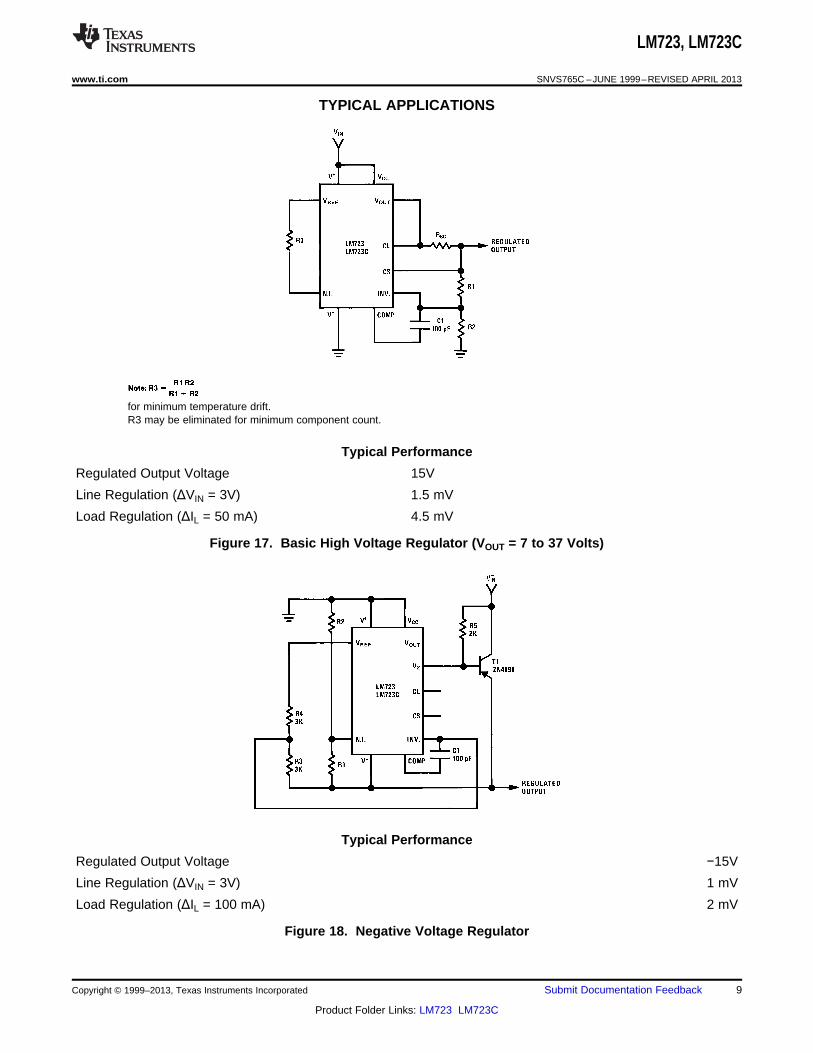
TYPICAL APPLICATIONS
for minimum temperature drift.R3 may be eliminated for minimum component count.
Typical Performance
Regulated Output Voltage 15V
Line Regulation (ΔVIN = 3V) 1.5 mV
Load Regulation (ΔIL = 50 mA) 4.5 mV
Figure 17. Basic High Voltage Regulator (VOUT = 7 to 37 Volts)
Typical Performance
Regulated Output Voltage −15V
Line Regulation (ΔVIN = 3V) 1 mV
Load Regulation (ΔIL = 100 mA) 2 mV
Figure 18. Negative Voltage Regulator
Copyright © 1999–2013, Texas Instruments Incorporated Submit Documentation Feedback 9
Product Folder Links: LM723 LM723C
LM723, LM723C
SNVS765C –JUNE 1999–REVISED APRIL 2013 www.ti.com
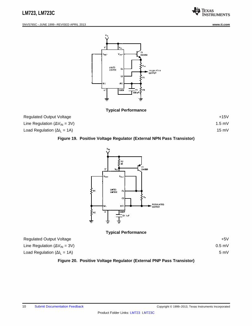
Typical Performance
Regulated Output Voltage +15V
Line Regulation (ΔVIN = 3V) 1.5 mV
Load Regulation (ΔIL = 1A) 15 mV
Figure 19. Positive Voltage Regulator (External NPN Pass Transistor)
Typical Performance
Regulated Output Voltage +5V
Line Regulation (ΔVIN = 3V) 0.5 mV
Load Regulation (ΔIL = 1A) 5 mV
Figure 20. Positive Voltage Regulator (External PNP Pass Transistor)
10 Submit Documentation Feedback Copyright © 1999–2013, Texas Instruments Incorporated
Product Folder Links: LM723 LM723C
LM723, LM723C
www.ti.com SNVS765C –JUNE 1999–REVISED APRIL 2013
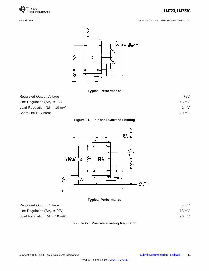
Typical Performance
Regulated Output Voltage +5V
Line Regulation (ΔVIN = 3V) 0.5 mV
Load Regulation (ΔIL = 10 mA) 1 mV
Short Circuit Current 20 mA
Figure 21. Foldback Current Limiting
Typical Performance
Regulated Output Voltage +50V
Line Regulation (ΔVIN = 20V) 15 mV
Load Regulation (ΔIL = 50 mA) 20 mV
Figure 22. Positive Floating Regulator
Copyright © 1999–2013, Texas Instruments Incorporated Submit Documentation Feedback 11
Product Folder Links: LM723 LM723C
LM723, LM723C
SNVS765C –JUNE 1999–REVISED APRIL 2013 www.ti.com
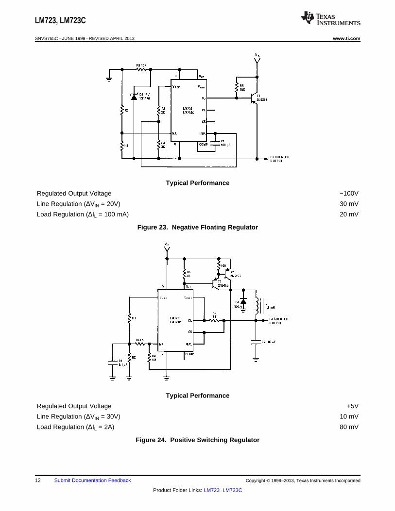
Typical Performance
Regulated Output Voltage −100V
Line Regulation (ΔVIN = 20V) 30 mV
Load Regulation (ΔIL = 100 mA) 20 mV
Figure 23. Negative Floating Regulator
Typical Performance
Regulated Output Voltage +5V
Line Regulation (ΔVIN = 30V) 10 mV
Load Regulation (ΔIL = 2A) 80 mV
Figure 24. Positive Switching Regulator
12 Submit Documentation Feedback Copyright © 1999–2013, Texas Instruments Incorporated
Product Folder Links: LM723 LM723C
LM723, LM723C
www.ti.com SNVS765C –JUNE 1999–REVISED APRIL 2013
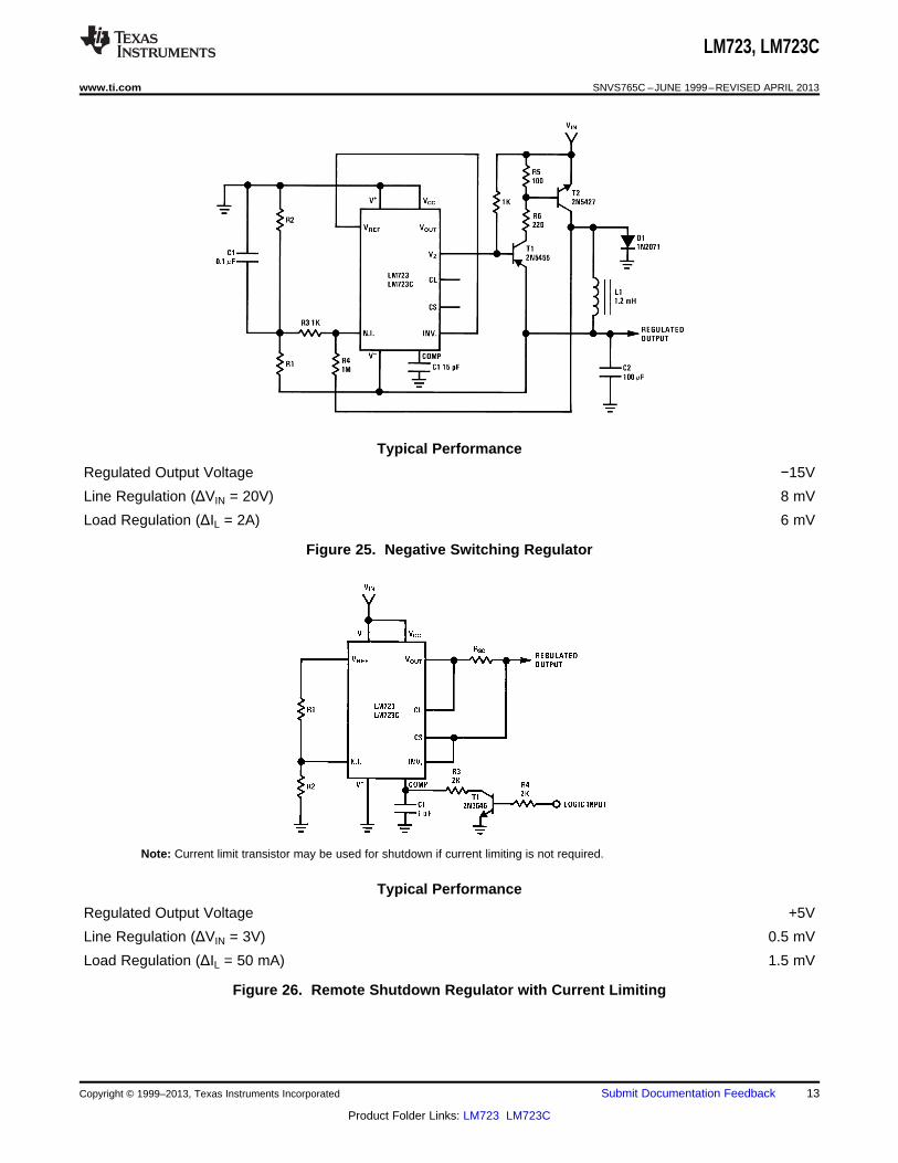
Typical Performance
Regulated Output Voltage −15V
Line Regulation (ΔVIN = 20V) 8 mV
Load Regulation (ΔIL = 2A) 6 mV
Figure 25. Negative Switching Regulator
Note: Current limit transistor may be used for shutdown if current limiting is not required.
Typical Performance
Regulated Output Voltage +5V
Line Regulation (ΔVIN = 3V) 0.5 mV
Load Regulation (ΔIL = 50 mA) 1.5 mV
Figure 26. Remote Shutdown Regulator with Current Limiting
Copyright © 1999–2013, Texas Instruments Incorporated Submit Documentation Feedback 13
Product Folder Links: LM723 LM723C
LM723, LM723C
SNVS765C –JUNE 1999–REVISED APRIL 2013 www.ti.com
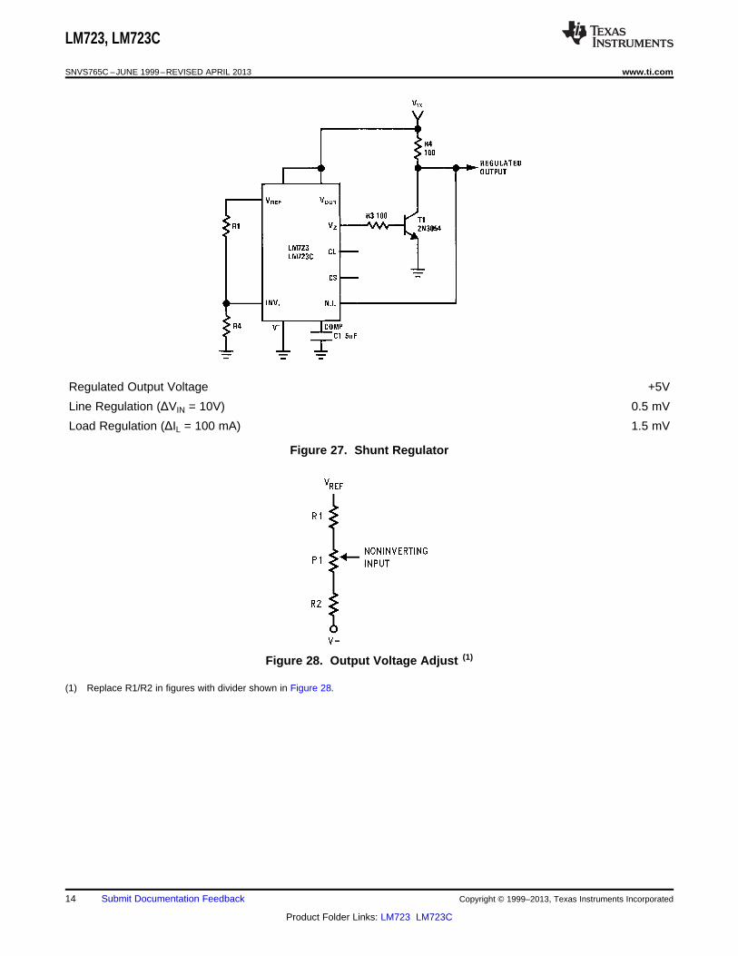
Regulated Output Voltage +5V
Line Regulation (ΔVIN = 10V) 0.5 mV
Load Regulation (ΔIL = 100 mA) 1.5 mV
Figure 27. Shunt Regulator
Figure 28. Output Voltage Adjust (1)
(1) Replace R1/R2 in figures with divider shown in Figure 28.
14 Submit Documentation Feedback Copyright © 1999–2013, Texas Instruments Incorporated
Product Folder Links: LM723 LM723C
LM723, LM723C
www.ti.com SNVS765C –JUNE 1999–REVISED APRIL 2013
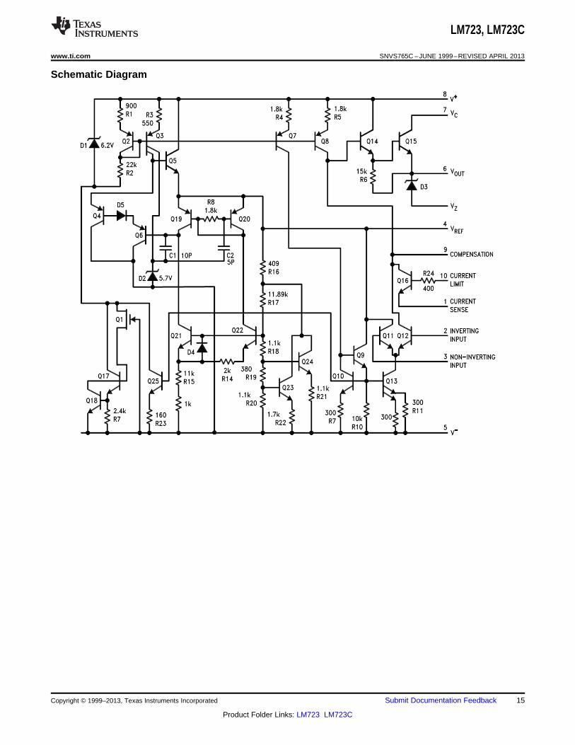
Schematic Diagram
Copyright © 1999–2013, Texas Instruments Incorporated Submit Documentation Feedback 15
Product Folder Links: LM723 LM723C
LM723, LM723C
SNVS765C –JUNE 1999–REVISED APRIL 2013 www.ti.com
REVISION HISTORY
Changes from Revision B (April 2013) to Revision C Page
• Changed layout of National Data Sheet to TI format .......................................................................................................... 15
16 Submit Documentation Feedback Copyright © 1999–2013, Texas Instruments Incorporated
Product Folder Links: LM723 LM723C
PACKAGE OPTION ADDENDUM
www.ti.com 17-Feb-2015
Addendum-Page 1
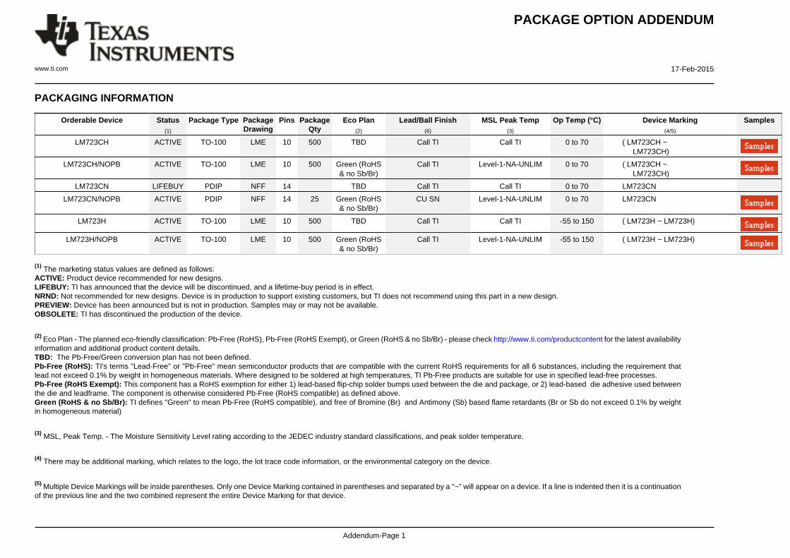
PACKAGING INFORMATION
Orderable Device Status(1)
Package Type PackageDrawing
Pins PackageQty
Eco Plan(2)
Lead/Ball Finish(6)
MSL Peak Temp(3)
Op Temp (°C) Device Marking(4/5)
Samples
LM723CH ACTIVE TO-100 LME 10 500 TBD Call TI Call TI 0 to 70 ( LM723CH ~ LM723CH)
LM723CH/NOPB ACTIVE TO-100 LME 10 500 Green (RoHS& no Sb/Br)
Call TI Level-1-NA-UNLIM 0 to 70 ( LM723CH ~ LM723CH)
LM723CN LIFEBUY PDIP NFF 14 TBD Call TI Call TI 0 to 70 LM723CN
LM723CN/NOPB ACTIVE PDIP NFF 14 25 Green (RoHS& no Sb/Br)
CU SN Level-1-NA-UNLIM 0 to 70 LM723CN
LM723H ACTIVE TO-100 LME 10 500 TBD Call TI Call TI -55 to 150 ( LM723H ~ LM723H)
LM723H/NOPB ACTIVE TO-100 LME 10 500 Green (RoHS& no Sb/Br)
Call TI Level-1-NA-UNLIM -55 to 150 ( LM723H ~ LM723H)
(1) The marketing status values are defined as follows:ACTIVE: Product device recommended for new designs.LIFEBUY: TI has announced that the device will be discontinued, and a lifetime-buy period is in effect.NRND: Not recommended for new designs. Device is in production to support existing customers, but TI does not recommend using this part in a new design.PREVIEW: Device has been announced but is not in production. Samples may or may not be available.OBSOLETE: TI has discontinued the production of the device.
(2) Eco Plan - The planned eco-friendly classification: Pb-Free (RoHS), Pb-Free (RoHS Exempt), or Green (RoHS & no Sb/Br) - please check http://www.ti.com/productcontent for the latest availabilityinformation and additional product content details.TBD: The Pb-Free/Green conversion plan has not been defined.Pb-Free (RoHS): TI's terms "Lead-Free" or "Pb-Free" mean semiconductor products that are compatible with the current RoHS requirements for all 6 substances, including the requirement thatlead not exceed 0.1% by weight in homogeneous materials. Where designed to be soldered at high temperatures, TI Pb-Free products are suitable for use in specified lead-free processes.Pb-Free (RoHS Exempt): This component has a RoHS exemption for either 1) lead-based flip-chip solder bumps used between the die and package, or 2) lead-based die adhesive used betweenthe die and leadframe. The component is otherwise considered Pb-Free (RoHS compatible) as defined above.Green (RoHS & no Sb/Br): TI defines "Green" to mean Pb-Free (RoHS compatible), and free of Bromine (Br) and Antimony (Sb) based flame retardants (Br or Sb do not exceed 0.1% by weightin homogeneous material)
(3) MSL, Peak Temp. - The Moisture Sensitivity Level rating according to the JEDEC industry standard classifications, and peak solder temperature.
(4) There may be additional marking, which relates to the logo, the lot trace code information, or the environmental category on the device.
(5) Multiple Device Markings will be inside parentheses. Only one Device Marking contained in parentheses and separated by a "~" will appear on a device. If a line is indented then it is a continuationof the previous line and the two combined represent the entire Device Marking for that device.
PACKAGE OPTION ADDENDUM
www.ti.com 17-Feb-2015
Addendum-Page 2
(6) Lead/Ball Finish - Orderable Devices may have multiple material finish options. Finish options are separated by a vertical ruled line. Lead/Ball Finish values may wrap to two lines if the finishvalue exceeds the maximum column width.
Important Information and Disclaimer:The information provided on this page represents TI's knowledge and belief as of the date that it is provided. TI bases its knowledge and belief on informationprovided by third parties, and makes no representation or warranty as to the accuracy of such information. Efforts are underway to better integrate information from third parties. TI has taken andcontinues to take reasonable steps to provide representative and accurate information but may not have conducted destructive testing or chemical analysis on incoming materials and chemicals.TI and TI suppliers consider certain information to be proprietary, and thus CAS numbers and other limited information may not be available for release.
In no event shall TI's liability arising out of such information exceed the total purchase price of the TI part(s) at issue in this document sold by TI to Customer on an annual basis.
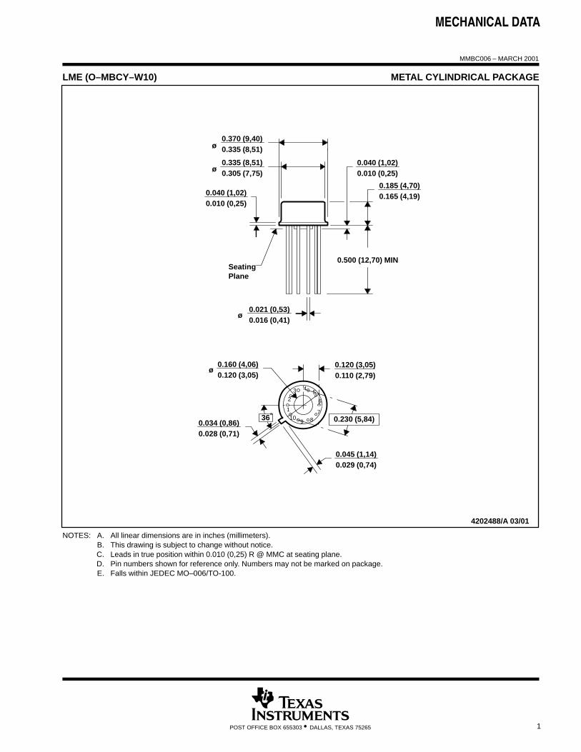
MECHANICAL DATA
MMBC006 – MARCH 2001
1POST OFFICE BOX 655303 • DALLAS, TEXAS 75265
LME (O–MBCY–W10) METAL CYLINDRICAL PACKAGE
78
4202488/A 03/01
0.335 (8,51)0.370 (9,40)
0.335 (8,51)0.305 (7,75)
0.185 (4,70)0.165 (4,19)
0.500 (12,70) MIN
0.010 (0,25)0.040 (1,02)
0.040 (1,02)0.010 (0,25)
0.016 (0,41)0.021 (0,53)
0.045 (1,14)0.029 (0,74)
0.028 (0,71)0.034 (0,86)
0.120 (3,05)0.160 (4,06) 0.120 (3,05)
0.110 (2,79)
ø
ø
ø
ø
SeatingPlane
36°
3
1
109
45
62
0.230 (5,84)
NOTES: A. All linear dimensions are in inches (millimeters).B. This drawing is subject to change without notice.C. Leads in true position within 0.010 (0,25) R @ MMC at seating plane.D. Pin numbers shown for reference only. Numbers may not be marked on package.E. Falls within JEDEC MO–006/TO-100.
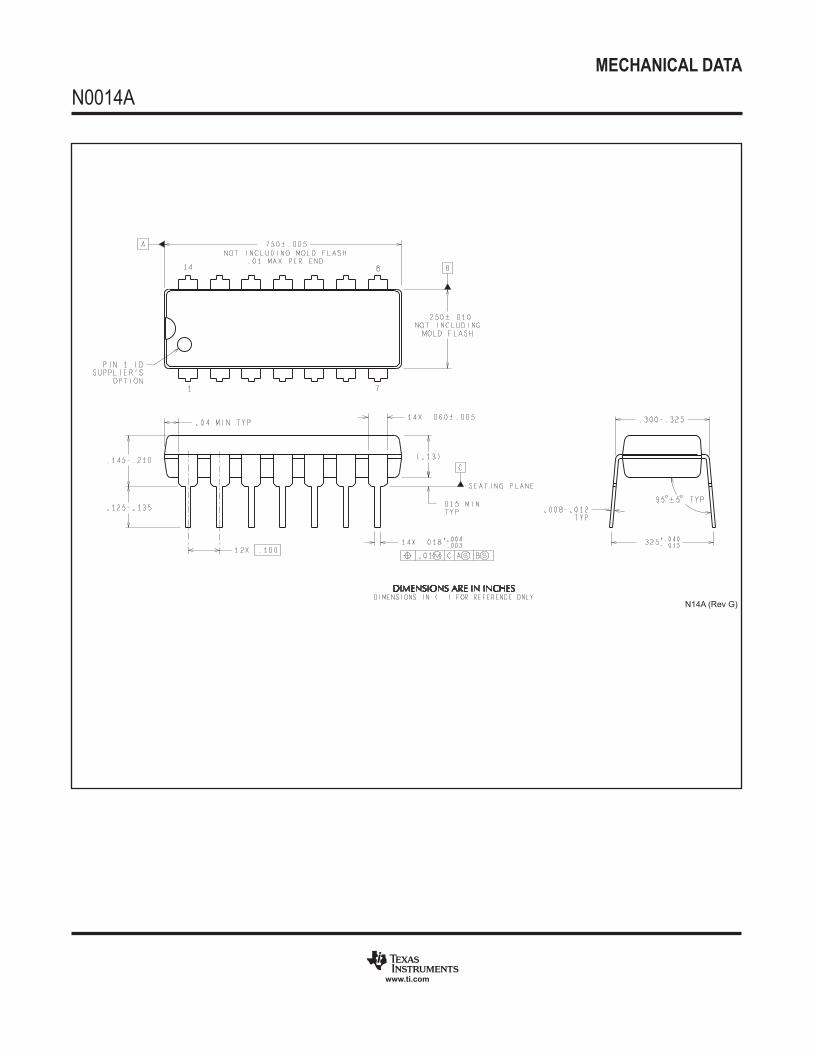
MECHANICAL DATA
N0014A
www.ti.com
N14A (Rev G)
IMPORTANT NOTICE
Texas Instruments Incorporated and its subsidiaries (TI) reserve the right to make corrections, enhancements, improvements and otherchanges to its semiconductor products and services per JESD46, latest issue, and to discontinue any product or service per JESD48, latestissue. Buyers should obtain the latest relevant information before placing orders and should verify that such information is current andcomplete. All semiconductor products (also referred to herein as “components”) are sold subject to TI’s terms and conditions of salesupplied at the time of order acknowledgment.TI warrants performance of its components to the specifications applicable at the time of sale, in accordance with the warranty in TI’s termsand conditions of sale of semiconductor products. Testing and other quality control techniques are used to the extent TI deems necessaryto support this warranty. Except where mandated by applicable law, testing of all parameters of each component is not necessarilyperformed.TI assumes no liability for applications assistance or the design of Buyers’ products. Buyers are responsible for their products andapplications using TI components. To minimize the risks associated with Buyers’ products and applications, Buyers should provideadequate design and operating safeguards.TI does not warrant or represent that any license, either express or implied, is granted under any patent right, copyright, mask work right, orother intellectual property right relating to any combination, machine, or process in which TI components or services are used. Informationpublished by TI regarding third-party products or services does not constitute a license to use such products or services or a warranty orendorsement thereof. Use of such information may require a license from a third party under the patents or other intellectual property of thethird party, or a license from TI under the patents or other intellectual property of TI.Reproduction of significant portions of TI information in TI data books or data sheets is permissible only if reproduction is without alterationand is accompanied by all associated warranties, conditions, limitations, and notices. TI is not responsible or liable for such altereddocumentation. Information of third parties may be subject to additional restrictions.Resale of TI components or services with statements different from or beyond the parameters stated by TI for that component or servicevoids all express and any implied warranties for the associated TI component or service and is an unfair and deceptive business practice.TI is not responsible or liable for any such statements.Buyer acknowledges and agrees that it is solely responsible for compliance with all legal, regulatory and safety-related requirementsconcerning its products, and any use of TI components in its applications, notwithstanding any applications-related information or supportthat may be provided by TI. Buyer represents and agrees that it has all the necessary expertise to create and implement safeguards whichanticipate dangerous consequences of failures, monitor failures and their consequences, lessen the likelihood of failures that might causeharm and take appropriate remedial actions. Buyer will fully indemnify TI and its representatives against any damages arising out of the useof any TI components in safety-critical applications.In some cases, TI components may be promoted specifically to facilitate safety-related applications. With such components, TI’s goal is tohelp enable customers to design and create their own end-product solutions that meet applicable functional safety standards andrequirements. Nonetheless, such components are subject to these terms.No TI components are authorized for use in FDA Class III (or similar life-critical medical equipment) unless authorized officers of the partieshave executed a special agreement specifically governing such use.Only those TI components which TI has specifically designated as military grade or “enhanced plastic” are designed and intended for use inmilitary/aerospace applications or environments. Buyer acknowledges and agrees that any military or aerospace use of TI componentswhich have not been so designated is solely at the Buyer's risk, and that Buyer is solely responsible for compliance with all legal andregulatory requirements in connection with such use.TI has specifically designated certain components as meeting ISO/TS16949 requirements, mainly for automotive use. In any case of use ofnon-designated products, TI will not be responsible for any failure to meet ISO/TS16949.
Products ApplicationsAudio www.ti.com/audio Automotive and Transportation www.ti.com/automotiveAmplifiers amplifier.ti.com Communications and Telecom www.ti.com/communicationsData Converters dataconverter.ti.com Computers and Peripherals www.ti.com/computersDLP® Products www.dlp.com Consumer Electronics www.ti.com/consumer-appsDSP dsp.ti.com Energy and Lighting www.ti.com/energyClocks and Timers www.ti.com/clocks Industrial www.ti.com/industrialInterface interface.ti.com Medical www.ti.com/medicalLogic logic.ti.com Security www.ti.com/securityPower Mgmt power.ti.com Space, Avionics and Defense www.ti.com/space-avionics-defenseMicrocontrollers microcontroller.ti.com Video and Imaging www.ti.com/videoRFID www.ti-rfid.comOMAP Applications Processors www.ti.com/omap TI E2E Community e2e.ti.comWireless Connectivity www.ti.com/wirelessconnectivity
Mailing Address: Texas Instruments, Post Office Box 655303, Dallas, Texas 75265Copyright © 2015, Texas Instruments Incorporated


![Atmel 8-bit AVR Microcontroller with 2/4/8K Bytes In ...files.microjpm.webnode.com/200001398-94b6996aae... · ATtiny25/45/85 [DATASHEET] 2 2586Q–AVR–08/2013 1. Pin Configurations](https://img.pdfslide.net/doc/110x75/5aef7d037f8b9ad0618cdefe/atmel-8-bit-avr-microcontroller-with-248k-bytes-in-files-datasheet-2-2586qavr082013.jpg)