Embed Size (px)
Citation preview
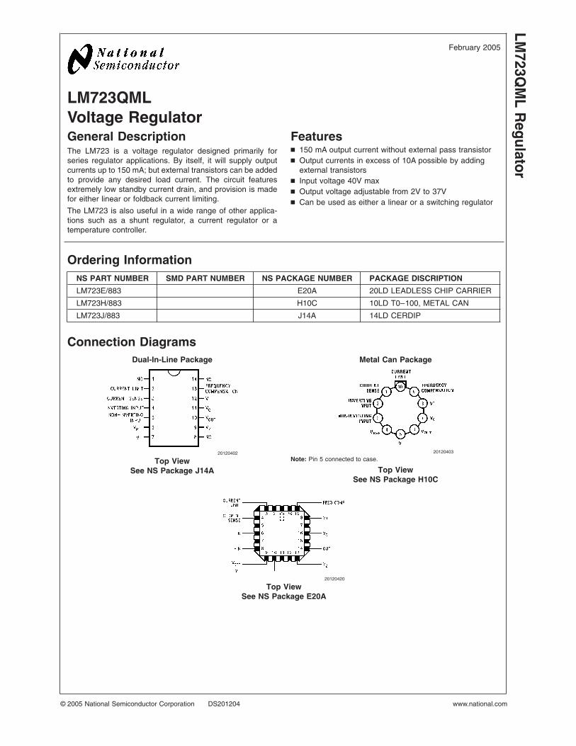
LM723QMLVoltage RegulatorGeneral DescriptionThe LM723 is a voltage regulator designed primarily forseries regulator applications. By itself, it will supply outputcurrents up to 150 mA; but external transistors can be addedto provide any desired load current. The circuit featuresextremely low standby current drain, and provision is madefor either linear or foldback current limiting.
The LM723 is also useful in a wide range of other applica-tions such as a shunt regulator, a current regulator or atemperature controller.
Featuresn 150 mA output current without external pass transistorn Output currents in excess of 10A possible by adding
external transistorsn Input voltage 40V maxn Output voltage adjustable from 2V to 37Vn Can be used as either a linear or a switching regulator
Ordering InformationNS PART NUMBER SMD PART NUMBER NS PACKAGE NUMBER PACKAGE DISCRIPTION
LM723E/883 E20A 20LD LEADLESS CHIP CARRIER
LM723H/883 H10C 10LD T0–100, METAL CAN
LM723J/883 J14A 14LD CERDIP
Connection DiagramsDual-In-Line Package Metal Can Package
20120402
Top ViewSee NS Package J14A
20120403
Note: Pin 5 connected to case.
Top ViewSee NS Package H10C
20120420
Top ViewSee NS Package E20A
February 2005LM
723QM
LR
egulator
© 2005 National Semiconductor Corporation DS201204 www.national.com
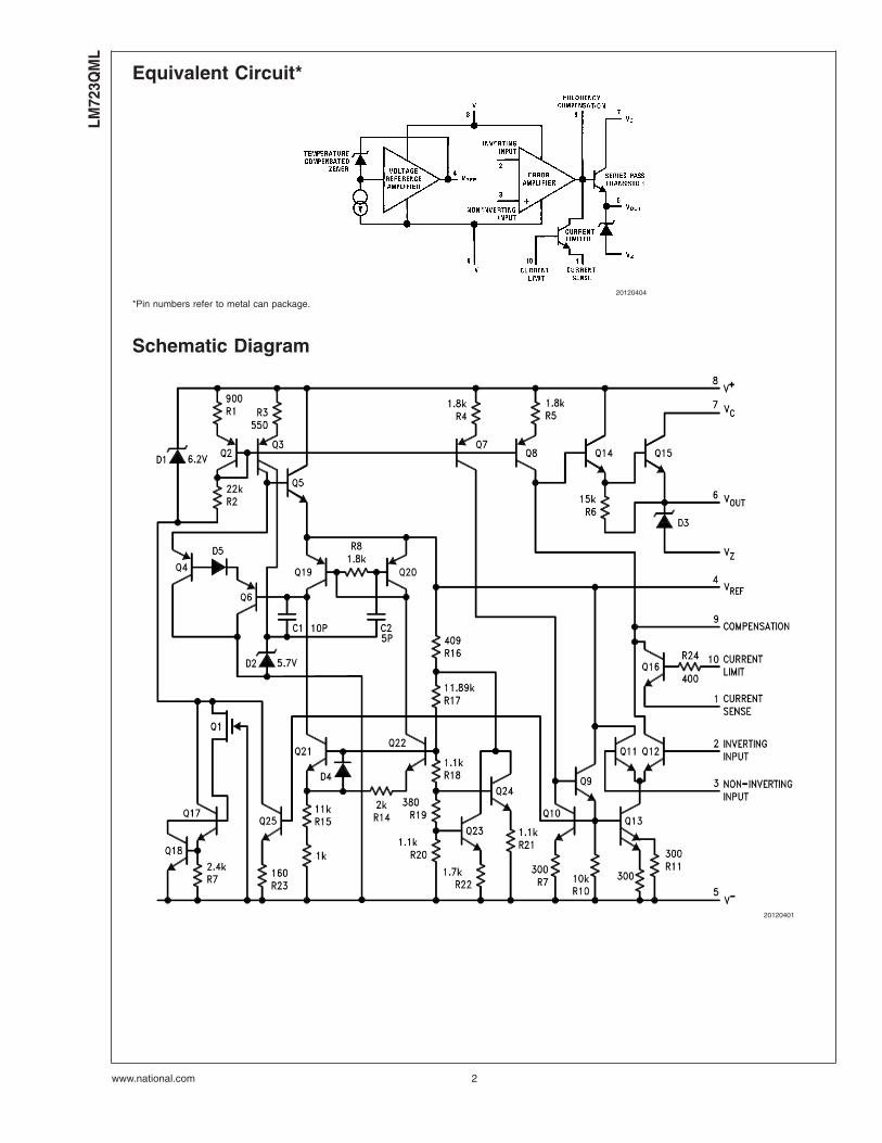
Equivalent Circuit*
20120404
*Pin numbers refer to metal can package.
Schematic Diagram
20120401
LM72
3QM
L
www.national.com 2
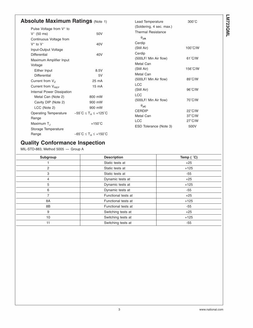
Absolute Maximum Ratings (Note 1)
Pulse Voltage from V+ toV− (50 ms) 50V
Continuous Voltage fromV+ to V− 40V
Input-Output VoltageDifferential 40V
Maximum Amplifier InputVoltage
Either InputDifferential
8.5V5V
Current from VZ 25 mA
Current from VREF 15 mA
Internal Power DissipationMetal Can (Note 2) 800 mW
Cavity DIP (Note 2) 900 mW
LCC (Note 2) 900 mW
Operating TemperatureRange
−55˚C ≤ TA ≤ +125˚C
Maximum TJ +150˚C
Storage TemperatureRange −65˚C ≤ TA ≤ +150˚C
Lead Temperature(Soldering, 4 sec. max.)
300˚C
Thermal Resistance
θJA
Cerdip(Still Air) 100˚C/W
Cerdip(500LF/ Min Air flow) 61˚C/W
Metal Can(Still Air) 156˚C/W
Metal Can(500LF/ Min Air flow) 89˚C/W
LCC(Still Air) 96˚C/W
LCC(500LF/ Min Air flow) 70˚C/W
θJC
CERDIPMetal CanLCC
22˚C/W37˚C/W27˚C/W
ESD Tolerance (Note 3) 500V
Quality Conformance InspectionMIL-STD-883, Method 5005 — Group A
Subgroup Description Temp ( ˚C)
1 Static tests at +25
2 Static tests at +125
3 Static tests at -55
4 Dynamic tests at +25
5 Dynamic tests at +125
6 Dynamic tests at -55
7 Functional tests at +25
8A Functional tests at +125
8B Functional tests at -55
9 Switching tests at +25
10 Switching tests at +125
11 Switching tests at -55
LM723Q
ML
www.national.com3
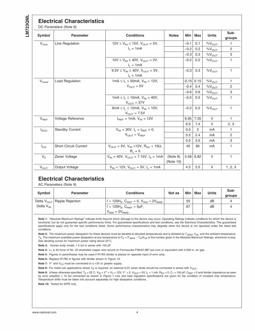
Electrical CharacteristicsDC Parameters (Note 9)
Symbol Parameter Conditions Notes Min Max UnitsSub-
groups
Vrline Line Regulation 12V ≤ VIN ≤ 15V, VOUT = 5V,IL = 1mA
−0.1 0.1 %VOUT 1
−0.2 0.2 %VOUT 2
−0.3 0.3 %VOUT 3
12V ≤ VIN ≤ 40V, VOUT = 2V,IL = 1mA
−0.2 0.2 %VOUT 1
9.5V ≤ VIN ≤ 40V, VOUT = 5V,IL = 1mA
−0.3 0.3 %VOUT 1
Vrload Load Regulation 1mA ≤ IL ≤ 50mA, VIN = 12V,VOUT = 5V
−0.15 0.15 %VOUT 1
−0.4 0.4 %VOUT 2
−0.6 0.6 %VOUT 3
1mA ≤ IL ≤ 10mA, VIN = 40V,VOUT = 37V
−0.5 0.5 %VOUT 1
6mA ≤ IL ≤ 12mA, VIN = 10V,VOUT = 7.5V
−0.2 0.2 %VOUT 1
VREF Voltage Reference IREF = 1mA, VIN = 12V 6.95 7.35 V 1
6.9 7.4 V 2, 3
ISCD Standby Current VIN = 30V, IL = IREF = 0,VOUT = VREF
0.5 3 mA 1
0.5 2.4 mA 2
0.5 3.5 mA 3
IOS Short Circuit Current VOUT = 5V, VIN =12V, RSC = 10Ω,RL = 0
45 85 mA 1
VZ Zener Voltage VIN = 40V, VOUT = 7.15V, IZ = 1mA (Note 8)(Note 10)
5.58 6.82 V 1
VOUT Output Voltage VIN = 12V, VOUT = 5V, IL = 1mA 4.5 5.5 V 1, 2, 3
Electrical CharacteristicsAC Parameters (Note 9)
Symbol Parameter Conditions Not es Min Max UnitsSub-
groups
Delta VOUT
Delta VIN
Ripple Rejection f = 120HZ, CREF = 0, VINS = 2VRMS 55 dB 4
f = 120HZ, CREF = 5µF,VINS = 2VRMS
67 dB 4
Note 1: “Absolute Maximum Ratings” indicate limits beyond which damage to the device may occur. Operating Ratings indicate conditions for which the device isfunctional, but do not guarantee specific performance limits. For guaranteed specifications and test conditions, see the Electrical Characteristics. The guaranteedspecifications apply only for the test conditions listed. Some performance characteristics may degrade when the device is not operated under the listed testconditions.
Note 2: The maximum power dissipation for these devices must be derated at elevated temperatures and is dictated by TJMAX, θJA, and the ambient temperature,TA. The maximum available power dissipation at any temperature is Pd = (TJMAX − TA)/θJA or the number given in the Absolute Maximum Ratings, whichever is less.See derating curves for maximum power rating above 25˚C.
Note 3: Human body model, 1.5 kΩ in series with 100 pF.
Note 4: L1 is 40 turns of No. 20 enameled copper wire wound on Ferroxcube P36/22-3B7 pot core or equivalent with 0.009 in. air gap.
Note 5: Figures in parentheses may be used if R1/R2 divider is placed on opposite input of error amp.
Note 6: Replace R1/R2 in figures with divider shown in Figure 13.
Note 7: V+ and VCC must be connected to a +3V or greater supply.
Note 8: For metal can applications where VZ is required, an external 6.2V zener diode should be connected in series with VOUT.
Note 9: Unless otherwise specified, TA = 25˚C, VIN = V+ = VC = 12V, V− = 0, VOUT = 5V, IL = 1 mA, RSC = 0, C1 = 100 pF, CREF = 0 and divider impedance as seenby error amplifier ≤ 10 kΩ connected as shown in Figure 1 Line and load regulation specifications are given for the condition of constant chip temperature.Temperature drifts must be taken into account separately for high dissipation conditions.
Note 10: Tested for DIPS only.
LM72
3QM
L
www.national.com 4
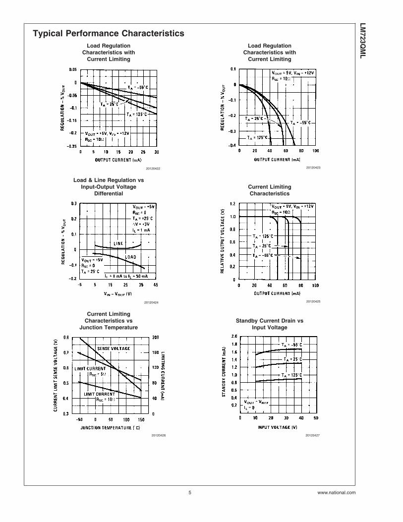
Typical Performance CharacteristicsLoad Regulation
Characteristics withCurrent Limiting
Load RegulationCharacteristics with
Current Limiting
20120422 20120423
Load & Line Regulation vsInput-Output Voltage
DifferentialCurrent LimitingCharacteristics
20120424 20120425
Current LimitingCharacteristics vs
Junction TemperatureStandby Current Drain vs
Input Voltage
20120426 20120427
LM723Q
ML
www.national.com5
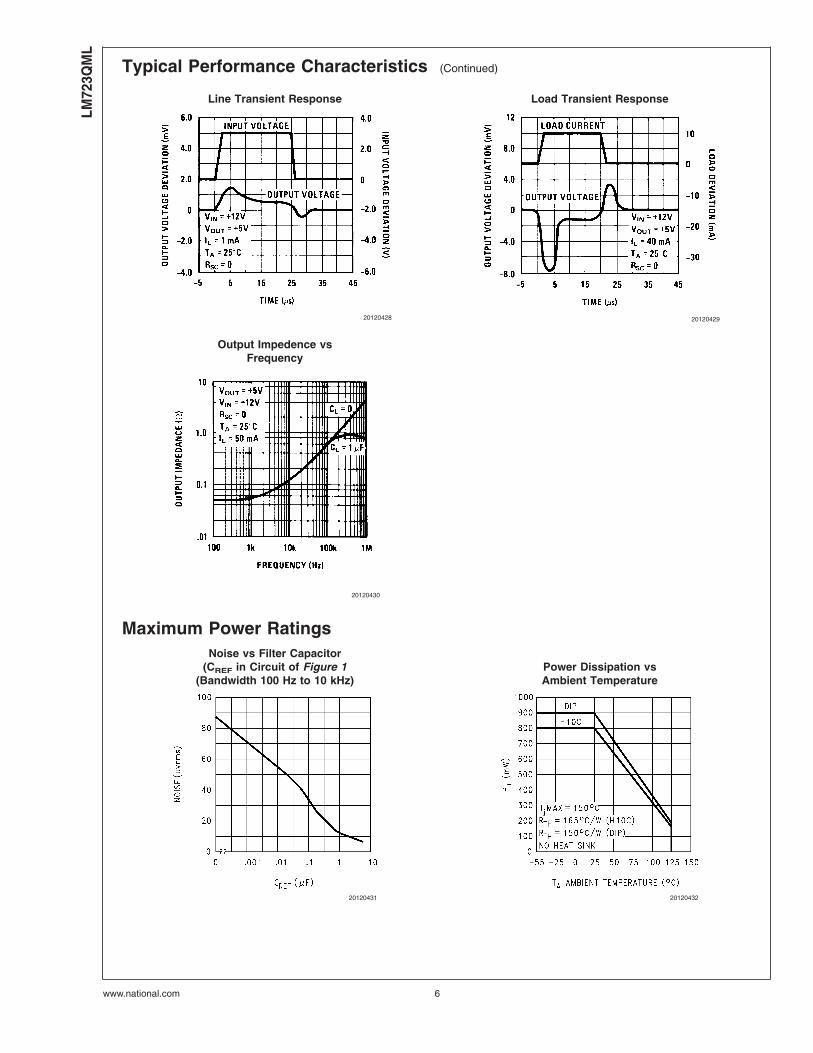
Typical Performance Characteristics (Continued)
Line Transient Response Load Transient Response
20120428 20120429
Output Impedence vsFrequency
20120430
Maximum Power RatingsNoise vs Filter Capacitor
(CREF in Circuit of Figure 1(Bandwidth 100 Hz to 10 kHz)
Power Dissipation vsAmbient Temperature
20120431 20120432
LM72
3QM
L
www.national.com 6
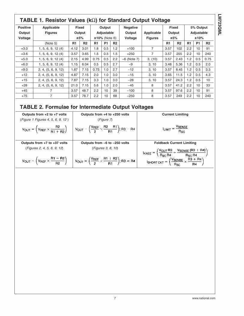
TABLE 1. Resistor Values (kΩ) for Standard Output VoltagePositive Applicable Fixed Output Negative Fixed 5% Output
Output Figures Output Adjustable Output Applicable Output Adjustable
Voltage ±5% ±10% (Note 6) Voltage Figures ±5% ±10%
(Note 5) R1 R2 R1 P1 R2 R1 R2 R1 P1 R2
+3.0 1, 5, 6, 9, 12 (4) 4.12 3.01 1.8 0.5 1.2 +100 7 3.57 102 2.2 10 91
+3.6 1, 5, 6, 9, 12 (4) 3.57 3.65 1.5 0.5 1.5 +250 7 3.57 255 2.2 10 240
+5.0 1, 5, 6, 9, 12 (4) 2.15 4.99 0.75 0.5 2.2 −6 (Note 7) 3, (10) 3.57 2.43 1.2 0.5 0.75
+6.0 1, 5, 6, 9, 12 (4) 1.15 6.04 0.5 0.5 2.7 −9 3, 10 3.48 5.36 1.2 0.5 2.0
+9.0 2, 4, (5, 6, 9, 12) 1.87 7.15 0.75 1.0 2.7 −12 3, 10 3.57 8.45 1.2 0.5 3.3
+12 2, 4, (5, 6, 9, 12) 4.87 7.15 2.0 1.0 3.0 −15 3, 10 3.65 11.5 1.2 0.5 4.3
+15 2, 4, (5, 6, 9, 12) 7.87 7.15 3.3 1.0 3.0 −28 3, 10 3.57 24.3 1.2 0.5 10
+28 2, 4, (5, 6, 9, 12) 21.0 7.15 5.6 1.0 2.0 −45 8 3.57 41.2 2.2 10 33
+45 7 3.57 48.7 2.2 10 39 −100 8 3.57 97.6 2.2 10 91
+75 7 3.57 78.7 2.2 10 68 −250 8 3.57 249 2.2 10 240
TABLE 2. Formulae for Intermediate Output VoltagesOutputs from +2 to +7 volts Outputs from +4 to +250 volts Current Limiting
(Figure 1 Figures 4, 5, 6, 9, 12 ) (Figure 7)
Outputs from +7 to +37 volts Outputs from −6 to −250 volts Foldback Current Limiting
(Figures 2, 4, 5, 6, 9, 12) (Figures 3, 8, 10)
LM723Q
ML
www.national.com7
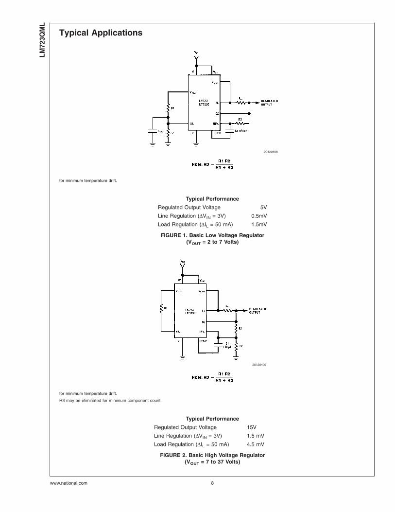
Typical Applications
20120408
for minimum temperature drift.
Typical Performance
Regulated Output Voltage 5V
Line Regulation (∆VIN = 3V) 0.5mV
Load Regulation (∆IL = 50 mA) 1.5mV
FIGURE 1. Basic Low Voltage Regulator(VOUT = 2 to 7 Volts)
20120409
for minimum temperature drift.
R3 may be eliminated for minimum component count.
Typical Performance
Regulated Output Voltage 15V
Line Regulation (∆VIN = 3V) 1.5 mV
Load Regulation (∆IL = 50 mA) 4.5 mV
FIGURE 2. Basic High Voltage Regulator(VOUT = 7 to 37 Volts)
LM72
3QM
L
www.national.com 8
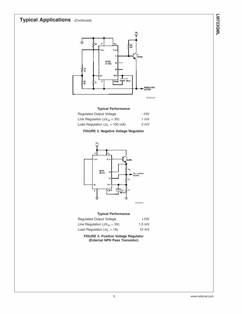
Typical Applications (Continued)
20120410
Typical Performance
Regulated Output Voltage −15V
Line Regulation (∆VIN = 3V) 1 mV
Load Regulation (∆IL = 100 mA) 2 mV
FIGURE 3. Negative Voltage Regulator
20120411
Typical Performance
Regulated Output Voltage +15V
Line Regulation (∆VIN = 3V) 1.5 mV
Load Regulation (∆IL = 1A) 15 mV
FIGURE 4. Positive Voltage Regulator(External NPN Pass Transistor)
LM723Q
ML
www.national.com9
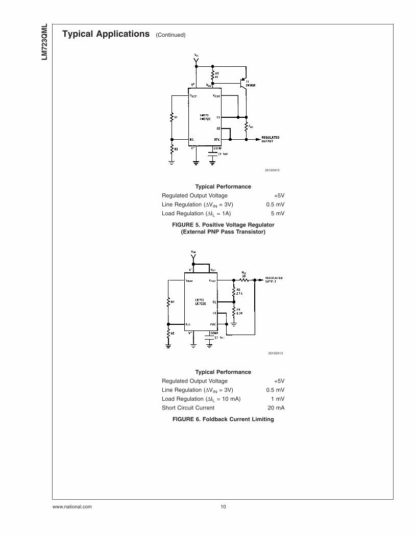
Typical Applications (Continued)
20120412
Typical Performance
Regulated Output Voltage +5V
Line Regulation (∆VIN = 3V) 0.5 mV
Load Regulation (∆IL = 1A) 5 mV
FIGURE 5. Positive Voltage Regulator(External PNP Pass Transistor)
20120413
Typical Performance
Regulated Output Voltage +5V
Line Regulation (∆VIN = 3V) 0.5 mV
Load Regulation (∆IL = 10 mA) 1 mV
Short Circuit Current 20 mA
FIGURE 6. Foldback Current Limiting
LM72
3QM
L
www.national.com 10
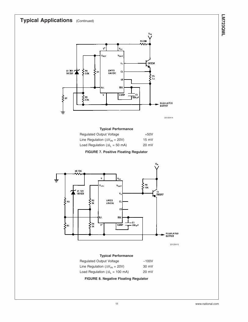
Typical Applications (Continued)
20120414
Typical Performance
Regulated Output Voltage +50V
Line Regulation (∆VIN = 20V) 15 mV
Load Regulation (∆IL = 50 mA) 20 mV
FIGURE 7. Positive Floating Regulator
20120415
Typical Performance
Regulated Output Voltage −100V
Line Regulation (∆VIN = 20V) 30 mV
Load Regulation (∆IL = 100 mA) 20 mV
FIGURE 8. Negative Floating Regulator
LM723Q
ML
www.national.com11
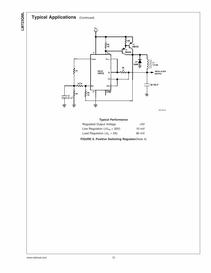
Typical Applications (Continued)
20120416
Typical Performance
Regulated Output Voltage +5V
Line Regulation (∆VIN = 30V) 10 mV
Load Regulation (∆IL = 2A) 80 mV
FIGURE 9. Positive Switching Regulator(Note 4)
LM72
3QM
L
www.national.com 12
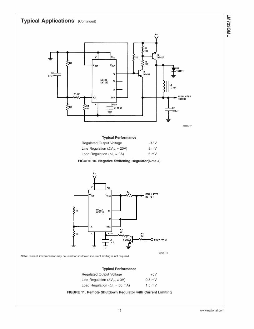
Typical Applications (Continued)
20120417
Typical Performance
Regulated Output Voltage −15V
Line Regulation (∆VIN = 20V) 8 mV
Load Regulation (∆IL = 2A) 6 mV
FIGURE 10. Negative Switching Regulator(Note 4)
20120418
Note: Current limit transistor may be used for shutdown if current limiting is not required.
Typical Performance
Regulated Output Voltage +5V
Line Regulation (∆VIN = 3V) 0.5 mV
Load Regulation (∆IL = 50 mA) 1.5 mV
FIGURE 11. Remote Shutdown Regulator with Current Limiting
LM723Q
ML
www.national.com13
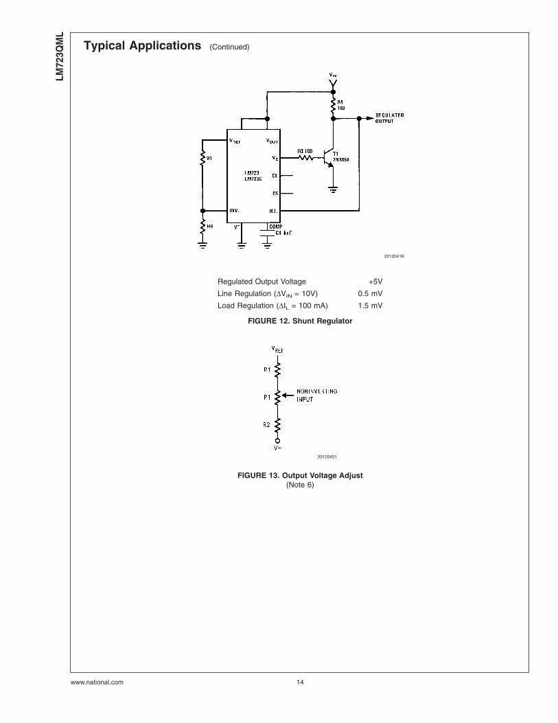
Typical Applications (Continued)
20120419
Regulated Output Voltage +5V
Line Regulation (∆VIN = 10V) 0.5 mV
Load Regulation (∆IL = 100 mA) 1.5 mV
FIGURE 12. Shunt Regulator
20120421
FIGURE 13. Output Voltage Adjust(Note 6)
LM72
3QM
L
www.national.com 14
Revision History SectionDateReleased Revision Section Originator Changes
02/15/05 A New Release, Corporate format L. Lytle 1 MDS data sheet converted into oneCorp. data sheet format. MNLM723-X,Rev. 1A0. MDS data sheet will bearchived. AC and Drift parametersremoved from specifcation because theyonly applied to the JAN B/S devices,covered in a separate datasheet.
LM723Q
ML
www.national.com15
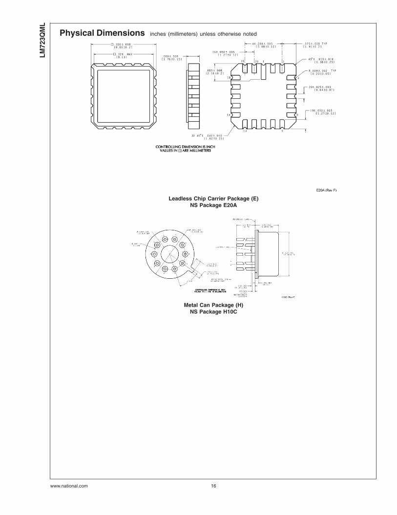
Physical Dimensions inches (millimeters) unless otherwise noted
Leadless Chip Carrier Package (E)NS Package E20A
Metal Can Package (H)NS Package H10C
LM72
3QM
L
www.national.com 16
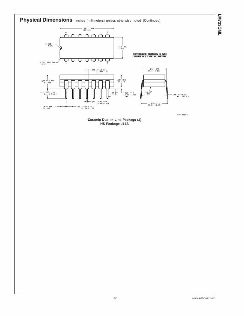
Physical Dimensions inches (millimeters) unless otherwise noted (Continued)
Ceramic Dual-In-Line Package (J)NS Package J14A
LM723Q
ML
www.national.com17
National does not assume any responsibility for use of any circuitry described, no circuit patent licenses are implied and National reservesthe right at any time without notice to change said circuitry and specifications.
For the most current product information visit us at www.national.com.
LIFE SUPPORT POLICY
NATIONAL’S PRODUCTS ARE NOT AUTHORIZED FOR USE AS CRITICAL COMPONENTS IN LIFE SUPPORT DEVICES OR SYSTEMSWITHOUT THE EXPRESS WRITTEN APPROVAL OF THE PRESIDENT AND GENERAL COUNSEL OF NATIONAL SEMICONDUCTORCORPORATION. As used herein:
1. Life support devices or systems are devices or systemswhich, (a) are intended for surgical implant into the body, or(b) support or sustain life, and whose failure to perform whenproperly used in accordance with instructions for useprovided in the labeling, can be reasonably expected to resultin a significant injury to the user.
2. A critical component is any component of a life supportdevice or system whose failure to perform can be reasonablyexpected to cause the failure of the life support device orsystem, or to affect its safety or effectiveness.
BANNED SUBSTANCE COMPLIANCE
National Semiconductor manufactures products and uses packing materials that meet the provisions of the Customer ProductsStewardship Specification (CSP-9-111C2) and the Banned Substances and Materials of Interest Specification (CSP-9-111S2) and containno ‘‘Banned Substances’’ as defined in CSP-9-111S2.
National SemiconductorAmericas CustomerSupport CenterEmail: [email protected]: 1-800-272-9959
National SemiconductorEurope Customer Support Center
Fax: +49 (0) 180-530 85 86Email: [email protected]
Deutsch Tel: +49 (0) 69 9508 6208English Tel: +44 (0) 870 24 0 2171Français Tel: +33 (0) 1 41 91 8790
National SemiconductorAsia Pacific CustomerSupport CenterEmail: [email protected]
National SemiconductorJapan Customer Support CenterFax: 81-3-5639-7507Email: [email protected]: 81-3-5639-7560
www.national.com
LM72
3QM
LR
egul
ator

This datasheet has been download from:
www.datasheetcatalog.com
Datasheets for electronics components.