Embed Size (px)
Citation preview
Lime Microsystems Limited
Surrey Tech Centre
Occam Road
The Surrey Research Park
Guildford, Surrey GU2 7YG
United Kingdom
Tel: +44 (0) 1483 685 063
Fax: +44 (0) 1428 656 662
e-mail: [email protected]
LMS7002M Field Programmable RF MIMO
Transceiver Integrated Circuit
- RF and Analog Measurement Results -
Chip version: LMS7002M
Chip revision: 01
Document version: 01
Document revision: 04
Last modified: 24/08/2015 10:50:00

1
Contents
1. Introduction ....................................................................................................................... 6
2. PLL Synthesizer Measurements ...................................................................................... 7 2.1 Frequency Coverage ..................................................................................................... 8 2.2 Phase Noise Measurements ........................................................................................ 10
2.3 PLL Spur Measurements ............................................................................................ 14
3. TX Measurements ........................................................................................................... 17 3.1 TX LPF Measurements .............................................................................................. 18 3.2 TX RF Gain Measurements........................................................................................ 21 3.3 TX OIP3 Measurements ............................................................................................. 22
3.4 Optimum TX ACPR Measurements .......................................................................... 24
3.5 Using the TSP NCO for Quick Linearity test ............................................................ 26
3.6 TX Output Harmonics ................................................................................................ 28 3.7 TX Noise Measurements ............................................................................................ 29 3.8 TX EVM Measurements ............................................................................................ 32 3.9 TX Output Power vs Frequency ................................................................................. 35 3.10 TX Noise Leakage into RX Band .............................................................................. 36 3.11 TX Peak Detector Measurements ............................................................................... 38 3.12 TX-TX TX-RX Isolation at RF Port .......................................................................... 40
4. RX Measurements ........................................................................................................... 41 4.1 RX Low Pass Filters ................................................................................................... 42
4.2 RX Noise Figure and Inband IIP3 Measurement ....................................................... 45 4.3 RX Out of band IIP2 and IIP3 Measurement ............................................................. 48
4.4 Variation of RX Gain and Noise Figure with Temperature ....................................... 52 4.5 RX LTE EVM Measurement ..................................................................................... 54
4.6 RX GSM Blocker EVM Measurements ..................................................................... 57 4.7 RX W-CDMA Blocker Test ....................................................................................... 60 4.8 Out of Band P1dB ...................................................................................................... 63
4.9 Comparison of LNA gains ......................................................................................... 64 4.10 RSSI ........................................................................................................................... 65
4.11 RX Gain step accuracy ............................................................................................... 67 4.12 RX LO Leakage at RF Port ........................................................................................ 69
5. Loop Back Measurements .............................................................................................. 70 5.1 Baseband Loopback ................................................................................................... 70 5.2 RF Loopback .............................................................................................................. 73
6. Miscellaneous Measurements ......................................................................................... 76 6.1 Power dissipation ....................................................................................................... 76
6.2 ‘On Chip’ LDO Measurments .................................................................................... 81 6.3 LMS7002M Internal LDO Noise Measurement ........................................................ 82
2
List of Figures
Figure 1. Simplified block diagram of the LMS7002M MIMO Software defined radio
transceiver chip. ........................................................................................................................... 6 Figure 2. Block diagram of PLL .................................................................................................. 7 Figure 3. Test bench for temperature measurements on the TX PLL .......................................... 8 Figure 4. Phase noise regions of a PLL synthesizer. .................................................................. 10 Figure 5. Test configuration for plateau region phase noise measurements .............................. 11
Figure 6. Plateau phase noise measurements for various LO frequencies with a 30.72MHz
TXCO crystal reference. ............................................................................................................ 12 Figure 7. Plateau phase noise measurements for various LO frequencies with a 52.00MHz
discrete crystal reference. ........................................................................................................... 12
Figure 8. Test configuration for measuring far out phase of the LMS7002M. .......................... 13 Figure 9. shows the amplitude of typical charge pump spurs 900MHz, RefFreq 30.72MHz. ... 14 Figure 10. shows the amplitude of typical charge pump spurs 900MHz, RefFreq 52.00MHz.. 14
Figure 11. shows the amplitude of typical charge pump spurs 2650MHz, RefFreq 30.72MHz.15 Figure 12. shows the amplitude of typical charge pump spurs 2650MHz, RefFreq 52.00MHz.15 Figure 13. shows the amplitude of DSM boundary spurs .......................................................... 15 Figure 14. shows the amplitude of TX and RX VCO coupling spurs at the TX output (relative
to the TX output) with varying RX frequency when TX LO=2649.6MHz ............................... 16 Figure 15. Block diagram of the Transmitter. ............................................................................ 18
Figure 16. Test bench used to test TX LPF Low Band .............................................................. 19 Figure 17. Filter responses of the TX LPF Low Band including de-emphasis pole. ................. 19 Figure 18. 10MHz Filter responses of the TX LPF Low Band with de-emphasis de-embedded
.................................................................................................................................................... 19
Figure 19. Test bench used to test TX LPF High Band ............................................................. 20 Figure 20. Filter responses of the TX LPF High Band .............................................................. 20 Figure 21. Test bench used to measure TX RF Gain Control .................................................... 21
Figure 22. Variation of output power and gain step accuracy with TX RF Gain Control. ........ 21 Figure 23. Test bench for measuring two tone OIP3. ................................................................ 22 Figure 24. Variation of OIP3 with output power at 900MHz as input level is varied for 3
different bias/gain settings in GUI ............................................................................................. 23 Figure 25. Test bench used for ACPR measurements with output power. ................................ 25
Figure 26. Measured ACPR vs output power with optimum gain controls. .............................. 25 Figure 27 Test bench for ‘quick linearity’ test. .......................................................................... 27 Figure 28 Testbench for measuring TX output harmonics ........................................................ 29
Figure 29 Test bench for transmitter noise measurement. ......................................................... 30 Figure 30. Test Bench used for TX EVM measurements with output power ............................ 32
Figure 31. LTE EVM Measurement at 860MHz ....................................................................... 33 Figure 32. LTE EVM Measurement at 2140MHz ..................................................................... 33
Figure 33. LTE EVM Measurement at 2610MHz ..................................................................... 34 Figure 34. Test bench for broadband software defined radio output power measurements. ..... 35 Figure 35. TX power output vs frequency for an unmatched evaluation board in broadband
operation with W-CDMA signal with -50dBc ACPR. ............................................................... 35 Figure 36. Test bench for measuring TX Noise in the RX band. ............................................... 36
Figure 37. Test bench used to measure peak detector performance. ......................................... 38 Figure 38. Typical output of peak detector with TX output power while varying the peak
detector preamplifier gain. ......................................................................................................... 39
3
Figure 39. Typical output of peak detector with TX output power while varying the peak
detector load. .............................................................................................................................. 39 Figure 40. Test bench for TX-TX and TX-RX coupling using the LMS7002M evaluation
board. .......................................................................................................................................... 40
Figure 41. Simplified block diagram of a single receiver channel. ............................................ 42 Figure 42. Test bench for testing low pass filters. ..................................................................... 42 Figure 43. Variable bandwith of low frequency low pass filter (LPFL) .................................... 43 Figure 44. 600kHz Low pass filter (LPFH) ............................................................................... 43 Figure 45. 2.5MHz Lowpass filter (LPFL) ................................................................................ 44
Figure 46. Variable bandwidth of the high frequency low pass filter (LPFH) .......................... 44 Figure 47. Test Bench for Noise Figure and Inband Linearity .................................................. 45 Figure 48. DSB Noise figure and inband IIP3 measurements vs gain at 800MHz .................... 45 Figure 49. DSB Noise figure and inband IIP3 measurements vs gain at 1850MHz .................. 46 Figure 50. DSB Noise figure and inband IIP3 measurements vs gain at 2600MHz .................. 46
Figure 51. Noise figure and S11 vs frequency for best match at 850MHz. ................................ 47 Figure 52. Noise figure and S11 vs frequency for minimum noise at 850MHz.......................... 47
Figure 53. Test bench for the out of band two tone receiver measurements .............................. 48 Figure 54. Comparsion of out of band IIP3 with gain of LMS7002M with a competing part at
850MHz with 600kHz LPF. ....................................................................................................... 50 Figure 55. Comparsion of out of band IIP3 with gain of LMS7002M with a competing part at
915MHz with 600kHz LPF ........................................................................................................ 50 Figure 56. Comparsion of out of band IIP3 with gain of LMS7002M with a competing part at
1980MHz with 2.5MHz LPF ..................................................................................................... 51
Figure 57. Comparsion of out of band IIP3 with gain of LMS7002M with a competing part at
2400MHz with 2.5MHz LPF ..................................................................................................... 51
Figure 58 Test bench for gain over temperature measurements ................................................ 52 Figure 59 Test Bench for noise figure over temperature measurements .................................... 52
Figure 60 Gain vs Frequency for different temperatres ............................................................. 53 Figure 61 Noise Figure vs Frequency for different temperatures .............................................. 53
Figure 62. Test bench for RX EVM measurements ................................................................... 54 Figure 63. Low IF EVM performance at 860MHz .................................................................... 55 Figure 64. Low IF LTE EVM at 2140MHz ............................................................................... 55
Figure 65. Low IF LTE EVM at 2600MHz ............................................................................... 56 Figure 66. Test bench used to measure RX EVM with CW blocker. ........................................ 57
Figure 67. RX GSM 900 EVM with CW blocker ...................................................................... 58 Figure 68. RX GSM 900 EVM with CW blocker ...................................................................... 58 Figure 69. RX GSM 1850 EVM with CW blocker .................................................................... 59 Figure 70. RX GSM 1850 EVM with CW blocker .................................................................... 59 Figure 71. Test bench configuration for W-CDMA blocker case. ............................................. 61
Figure 72. Spectrum of IF output without blocker present (signal -94dBm). ............................ 61
Figure 73. Spectrum of IF output with blocker present (signal -94dBm, blocker -15.6dBm). .. 62
Figure 74. W-CDMA Code Domain View (signal -94dB, blocker -15.6dBm) ......................... 62 Figure 75. Out of band P1dB compression point vs LNA gain control code. Measured with
2.5MHz LPF and blocker at 20MHz offset for different PGA gains. ........................................ 63 Figure 76. Variation of gain vs frequency of LNAH, LNAW and LNAL on LMS7002M
evaluation board with each input matched at each frequency. ................................................... 64
Figure 77. RSSI measurement test setup .................................................................................... 65 Figure 78. RSSI output value vs input power @ 2.14GHz ........................................................ 66 Figure 79. Test bench for measuring RX gain step accuracy ..................................................... 67
Figure 80. LNA Gain step accuracy for different RF frequencies ............................................. 68
4
Figure 81. Gain step accuracy for PGA at 1MHz and 10MHz. ................................................. 68
Figure 82. Test bench for measuring RX LO leakage. ............................................................... 69 Figure 83 Test bench for baseband loop back testing. ............................................................... 71 Figure 84 Frequency response of baseband loopback. ............................................................... 71
Figure 85. Test bench used to measure RF loopback. ................................................................ 73 Figure 86. Variation of RF loopback gain for two different frequencies. .................................. 74 Figure 87 Typical RX LPF response measured with RF loop back. .......................................... 74 Figure 88. Test bench used to measure power dissipation ......................................................... 78 Figure 89 Test configuration used to measure noise. ................................................................. 83
Figure 90 AC coupling circuit used for LDO noise measurement. ............................................ 83 Figure 91 Measured LDO noise of the LDO with LNA for different LDO modes. .................. 83

5
Revision History
Version 01r00
Started: 1 Nov, 2014
Finished: 11 Nov, 2014
Initial version.
Version 01r01
Started: 11 Nov, 2014
Finished: 19 Nov, 2014
Added: Sections 3.11, 3.12, 4.7, 4.11, 4.12, 6.2.
6
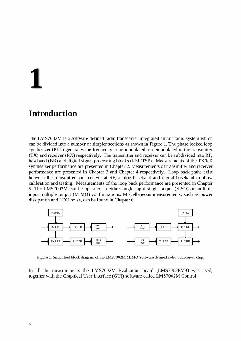
1 Introduction
The LMS7002M is a software defined radio transceiver integrated circuit radio system which
can be divided into a number of simpler sections as shown in Figure 1. The phase locked loop
synthesizer (PLL) generates the frequency to be modulated or demodulated in the transmitter
(TX) and receiver (RX) respectively. The transmitter and receiver can be subdivided into RF,
baseband (BB) and digital signal processing blocks (RSP/TSP). Measurements of the TX/RX
synthesizer performance are presented in Chapter 2. Measurements of transmitter and receiver
performance are presented in Chapter 3 and Chapter 4 respectively. Loop back paths exist
between the transmitter and receiver at RF, analog baseband and digital baseband to allow
calibration and testing. Measurements of the loop back performance are presented in Chapter
5. The LMS7002M can be operated in either single input single output (SISO) or multiple
input multiple output (MIMO) configurations. Miscellaneous measurements, such as power
dissipation and LDO noise, can be found in Chapter 6.
Rx PLL
Rx 1 RF Rx 1 BBRx 1
RSP
Rx 2 RF Rx 2 BBRx 2
RSP
Tx PLL
Tx 1
RSPTx 1 BB Tx 1 RF
Tx 2
RSPTx 2 BB Tx 2 RF
Figure 1. Simplified block diagram of the LMS7002M MIMO Software defined radio transceiver chip.
In all the measurements the LMS7002M Evaluation board (LMS7002EVB) was used,
together with the Graphical User Interface (GUI) software called LMS7002M Control.
7
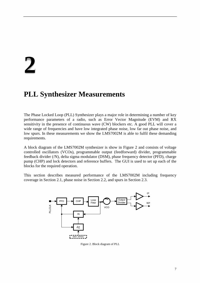
2 PLL Synthesizer Measurements
The Phase Locked Loop (PLL) Synthesizer plays a major role in determining a number of key
performance parameters of a radio, such as Error Vector Magnitude (EVM) and RX
sensitivity in the presence of continuous wave (CW) blockers etc. A good PLL will cover a
wide range of frequencies and have low integrated phase noise, low far out phase noise, and
low spurs. In these measurements we show the LMS7002M is able to fulfil these demanding
requirements.
A block diagram of the LMS7002M synthesizer is show in Figure 2 and consists of voltage
controlled oscillators (VCOs), programmable output (feedforward) divider, programmable
feedback divider (/N), delta sigma modulator (DSM), phase frequency detector (PFD), charge
pump (CHP) and lock detectors and reference buffers. The GUI is used to set up each of the
blocks for the required operation.
This section describes measured performance of the LMS7002M including frequency
coverage in Section 2.1, phase noise in Section 2.2, and spurs in Section 2.3.
PFD CHPLoop
Filter
/N
∆∑
~ Output
Divider
NINT, NFRAC
PL
LC
LK
0º
90º
VCO
Figure 2. Block diagram of PLL
8
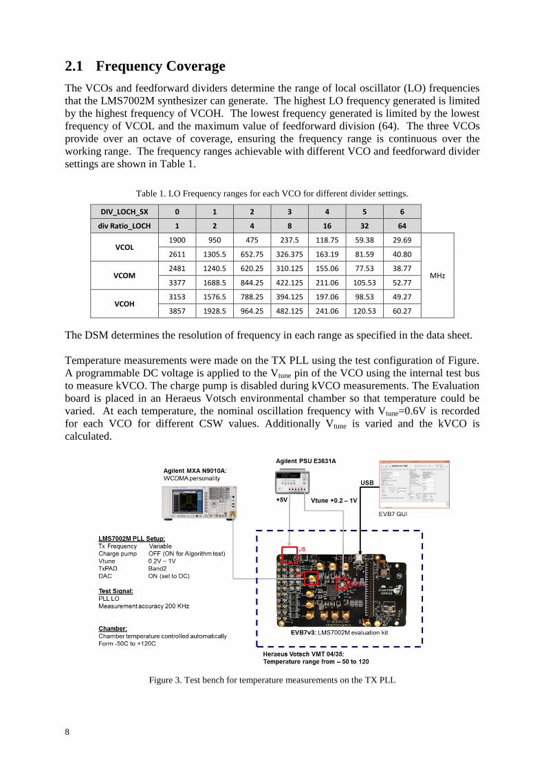
2.1 Frequency Coverage
The VCOs and feedforward dividers determine the range of local oscillator (LO) frequencies
that the LMS7002M synthesizer can generate. The highest LO frequency generated is limited
by the highest frequency of VCOH. The lowest frequency generated is limited by the lowest
frequency of VCOL and the maximum value of feedforward division (64). The three VCOs
provide over an octave of coverage, ensuring the frequency range is continuous over the
working range. The frequency ranges achievable with different VCO and feedforward divider
settings are shown in Table 1.
Table 1. LO Frequency ranges for each VCO for different divider settings.
DIV_LOCH_SX 0 1 2 3 4 5 6
div Ratio_LOCH 1 2 4 8 16 32 64
VCOL 1900 950 475 237.5 118.75 59.38 29.69
MHz
2611 1305.5 652.75 326.375 163.19 81.59 40.80
VCOM 2481 1240.5 620.25 310.125 155.06 77.53 38.77
3377 1688.5 844.25 422.125 211.06 105.53 52.77
VCOH 3153 1576.5 788.25 394.125 197.06 98.53 49.27
3857 1928.5 964.25 482.125 241.06 120.53 60.27
The DSM determines the resolution of frequency in each range as specified in the data sheet.
Temperature measurements were made on the TX PLL using the test configuration of Figure.
A programmable DC voltage is applied to the Vtune pin of the VCO using the internal test bus
to measure kVCO. The charge pump is disabled during kVCO measurements. The Evaluation
board is placed in an Heraeus Votsch environmental chamber so that temperature could be
varied. At each temperature, the nominal oscillation frequency with Vtune=0.6V is recorded
for each VCO for different CSW values. Additionally Vtune is varied and the kVCO is
calculated.
Figure 3. Test bench for temperature measurements on the TX PLL
9
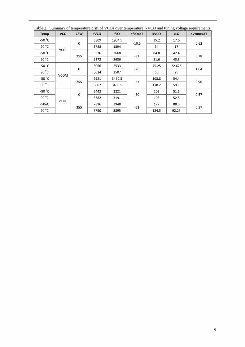
Table 2. Summary of temperature drift of VCOs over temperature, kVCO and tuning voltage requirements.
Temp VCO CSW fVCO fLO dfLO/dT kVCO kLO dVtune/dT
-50 oC
VCOL
0 3809 1904.5
-10.5 35.2 17.6
0.62 90
oC 3788 1894 34 17
-50 oC
255 5336 2668
-32 84.8 42.4
0.78 90
oC 5272 2636 81.6 40.8
-50 oC
VCOM
0 5066 2533
-26 45.25 22.625
1.04 90
oC 5014 2507 50 25
-50 oC
255 6921 3460.5
-57 108.8 54.4
0.96 90
oC 6807 3403.5 118.2 59.1
-50 oC
VCOH
0 6442 3221
-30 103 51.5
0.57 90
oC 6382 3191 105 52.5
-50oC 255
7896 3948 -53
177 88.5 0.57
90 oC 7790 3895 184.5 92.25
10
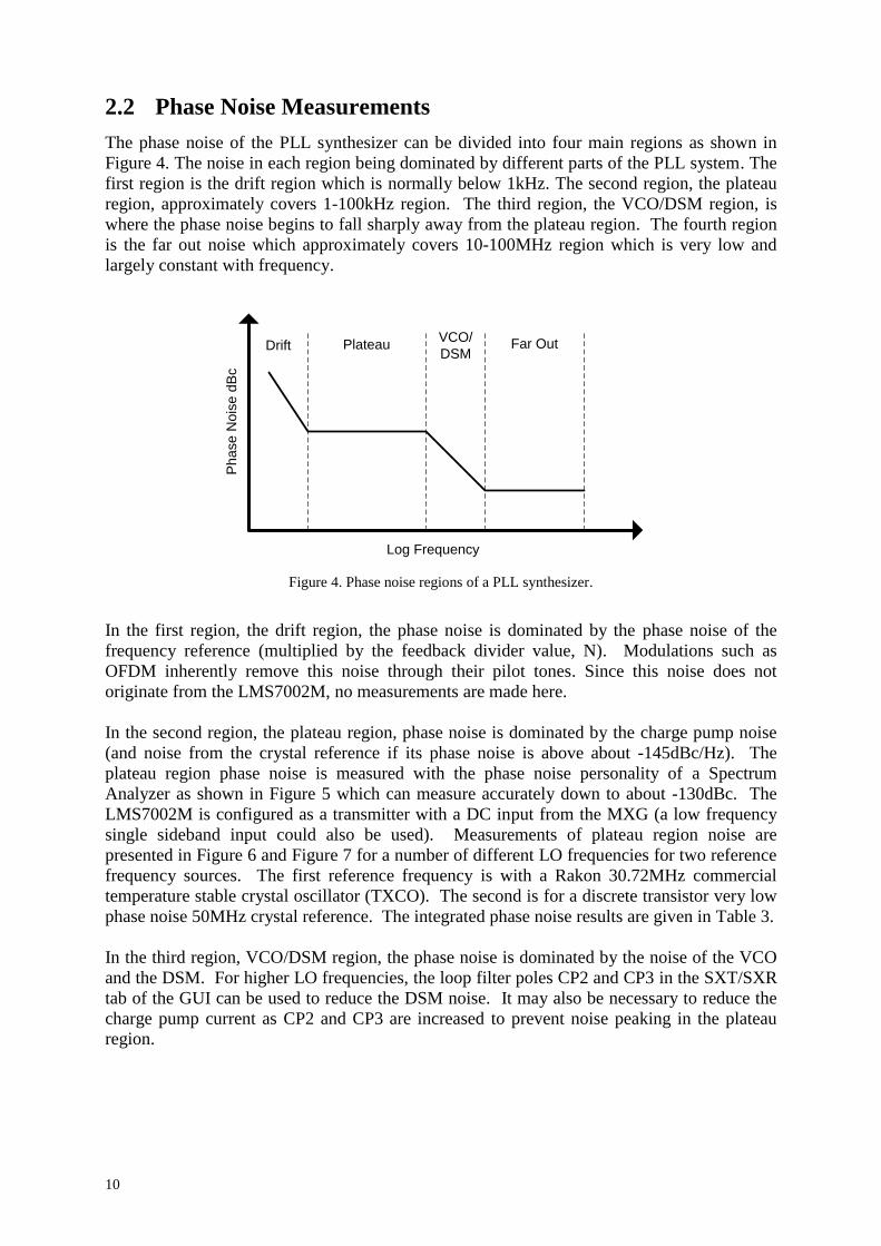
2.2 Phase Noise Measurements
The phase noise of the PLL synthesizer can be divided into four main regions as shown in
Figure 4. The noise in each region being dominated by different parts of the PLL system. The
first region is the drift region which is normally below 1kHz. The second region, the plateau
region, approximately covers 1-100kHz region. The third region, the VCO/DSM region, is
where the phase noise begins to fall sharply away from the plateau region. The fourth region
is the far out noise which approximately covers 10-100MHz region which is very low and
largely constant with frequency.
Ph
ase
No
ise
dB
c
Log Frequency
Drift PlateauVCO/
DSMFar Out
Figure 4. Phase noise regions of a PLL synthesizer.
In the first region, the drift region, the phase noise is dominated by the phase noise of the
frequency reference (multiplied by the feedback divider value, N). Modulations such as
OFDM inherently remove this noise through their pilot tones. Since this noise does not
originate from the LMS7002M, no measurements are made here.
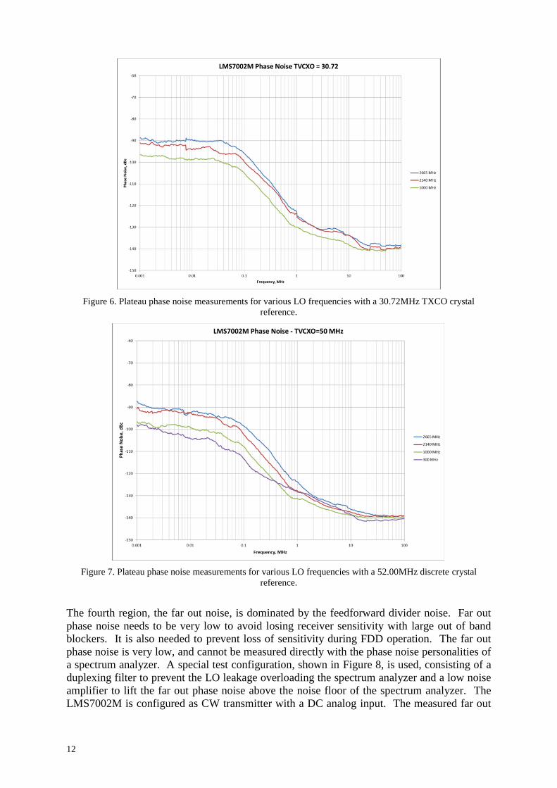
In the second region, the plateau region, phase noise is dominated by the charge pump noise
(and noise from the crystal reference if its phase noise is above about -145dBc/Hz). The
plateau region phase noise is measured with the phase noise personality of a Spectrum
Analyzer as shown in Figure 5 which can measure accurately down to about -130dBc. The
LMS7002M is configured as a transmitter with a DC input from the MXG (a low frequency
single sideband input could also be used). Measurements of plateau region noise are
presented in Figure 6 and Figure 7 for a number of different LO frequencies for two reference
frequency sources. The first reference frequency is with a Rakon 30.72MHz commercial
temperature stable crystal oscillator (TXCO). The second is for a discrete transistor very low
phase noise 50MHz crystal reference. The integrated phase noise results are given in Table 3.
In the third region, VCO/DSM region, the phase noise is dominated by the noise of the VCO
and the DSM. For higher LO frequencies, the loop filter poles CP2 and CP3 in the SXT/SXR
tab of the GUI can be used to reduce the DSM noise. It may also be necessary to reduce the
charge pump current as CP2 and CP3 are increased to prevent noise peaking in the plateau
region.

11
Figure 5. Test configuration for plateau region phase noise measurements
Table 3. Integrated phase noise for different Synthesizer frequencies (TXCO=50MHz)
Tx LO, MHz
PN@ 1kHz, dBc
PN@ 10kHz, dBc
PN@ 100kHz, dBc
PN@ 1MHz, dBc
PN@ 10MHz, dBc
Integrated PN, deg*
2665 -87.23 -92.54 -98.28 -123.63 -136.15 0.5
2140 90.71 -92.57 -102.45 -127.67 -137.46 0.4
1000 -96.46 -99.24 -107.78 -131.17 -138.8 0.2
300 -97.88 -104.08 -113.42 -128.14 -138.57 0.13
Table 4 Typical required integrated phase noise performance for OFDM
Modulation Required Integrated Phase
Noise
Application
OFDM QAM64 1o LTE, WiMAX
OFDM QAM256 0.5o CATV, DVB
OFDM QAM1024 0.25o DVB-C2
12
Figure 6. Plateau phase noise measurements for various LO frequencies with a 30.72MHz TXCO crystal
reference.
Figure 7. Plateau phase noise measurements for various LO frequencies with a 52.00MHz discrete crystal
reference.
The fourth region, the far out noise, is dominated by the feedforward divider noise. Far out
phase noise needs to be very low to avoid losing receiver sensitivity with large out of band
blockers. It is also needed to prevent loss of sensitivity during FDD operation. The far out
phase noise is very low, and cannot be measured directly with the phase noise personalities of
a spectrum analyzer. A special test configuration, shown in Figure 8, is used, consisting of a
duplexing filter to prevent the LO leakage overloading the spectrum analyzer and a low noise
amplifier to lift the far out phase noise above the noise floor of the spectrum analyzer. The
LMS7002M is configured as CW transmitter with a DC analog input. The measured far out
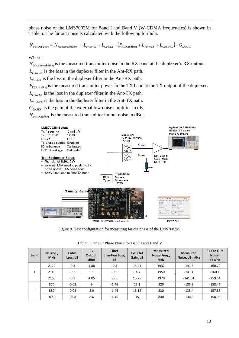
13
phase noise of the LMS7002M for Band I and Band V (W-CDMA frequencies) is shown in
Table 5. The far out noise is calculated with the following formula.
LNARXCableTXFilterTXdBmTXOutCableXFilterRXdBmMeasuredRdBcFarOut GLLPLLNN )()()(
Where:
)(dBmMeasuredRN is the measured transmitter noise in the RX band at the duplexer’s RX output.
FilterRXL is the loss in the duplexer filter in the Ant-RX path.
CableXL is the loss in the duplexer filter in the Ant-RX path.
)(dBmTXOutP is the measured transmitter power in the TX band at the TX output of the duplexer.
FilterTXL is the loss in the duplexer filter in the Ant-TX path.
CableTXL is the loss in the duplexer filter in the Ant-TX path.
LNARXG is the gain of the external low noise amplifier in dB.
)(dBcFarOutN is the measured transmitter far out noise in dBc.
Figure 8. Test configuration for measuring far out phase of the LMS7002M.
Table 5. Far Out Phase Noise for Band I and Band V
Band Tx Freq.,
MHz Cable
Loss, dB
Tx Output,
dBm
Filter Insertion Loss,
dB
Ext. LNA Gain, dB
Measured Noise Freq.,
MHz
Measured Noise, dBm/Hz
Tx Far-Out Noise, dBc/Hz
I
2122 -0.3 4.88 -0.5 15.41 1932 -141.3 -160.79
2140 -0.3 5.1 -0.5 14.7 1950 -141.1 -160.1
2160 -0.3 4.05 -0.5 15.25 1970 -141.01 -159.51
II
870 -0.08 9 -1.46 15.1 820 -135.9 -158.46
880 -0.08 8.9 -1.46 15.12 830 -135.4 -157.88
890 -0.08 8.6 -1.46 15 840 -136.9 -158.96
14
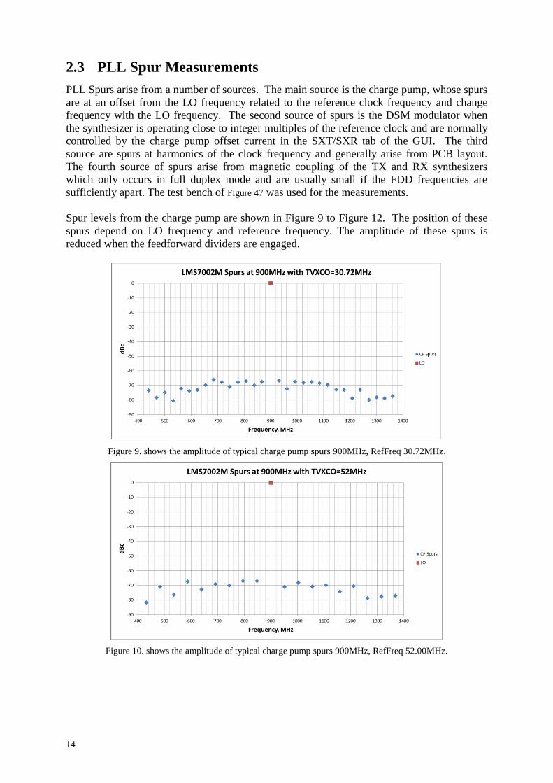
2.3 PLL Spur Measurements
PLL Spurs arise from a number of sources. The main source is the charge pump, whose spurs
are at an offset from the LO frequency related to the reference clock frequency and change
frequency with the LO frequency. The second source of spurs is the DSM modulator when
the synthesizer is operating close to integer multiples of the reference clock and are normally
controlled by the charge pump offset current in the SXT/SXR tab of the GUI. The third
source are spurs at harmonics of the clock frequency and generally arise from PCB layout.
The fourth source of spurs arise from magnetic coupling of the TX and RX synthesizers
which only occurs in full duplex mode and are usually small if the FDD frequencies are
sufficiently apart. The test bench of Figure 47 was used for the measurements.
Spur levels from the charge pump are shown in Figure 9 to Figure 12. The position of these
spurs depend on LO frequency and reference frequency. The amplitude of these spurs is
reduced when the feedforward dividers are engaged.
Figure 9. shows the amplitude of typical charge pump spurs 900MHz, RefFreq 30.72MHz.
Figure 10. shows the amplitude of typical charge pump spurs 900MHz, RefFreq 52.00MHz.
15
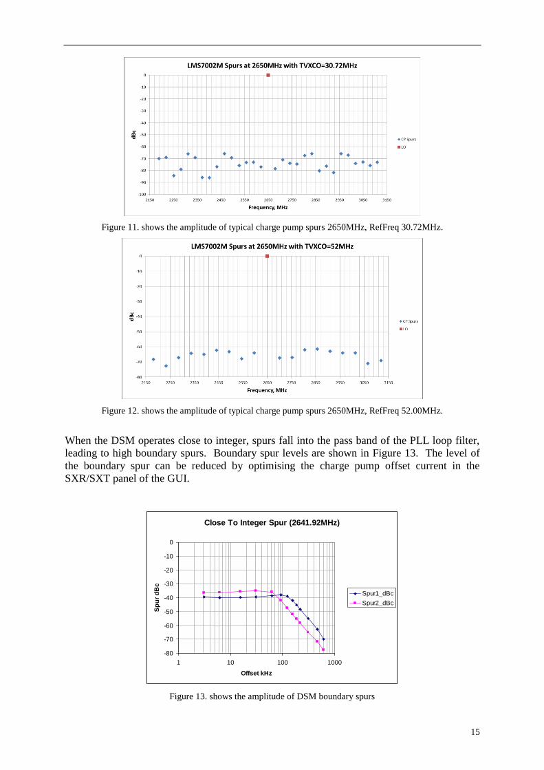
Figure 11. shows the amplitude of typical charge pump spurs 2650MHz, RefFreq 30.72MHz.
Figure 12. shows the amplitude of typical charge pump spurs 2650MHz, RefFreq 52.00MHz.
When the DSM operates close to integer, spurs fall into the pass band of the PLL loop filter,
leading to high boundary spurs. Boundary spur levels are shown in Figure 13. The level of
the boundary spur can be reduced by optimising the charge pump offset current in the
SXR/SXT panel of the GUI.
Figure 13. shows the amplitude of DSM boundary spurs
Close To Integer Spur (2641.92MHz)
-80
-70
-60
-50
-40
-30
-20
-10
0
1 10 100 1000
Offset kHz
Sp
ur
dB
c
Spur1_dBc
Spur2_dBc
16
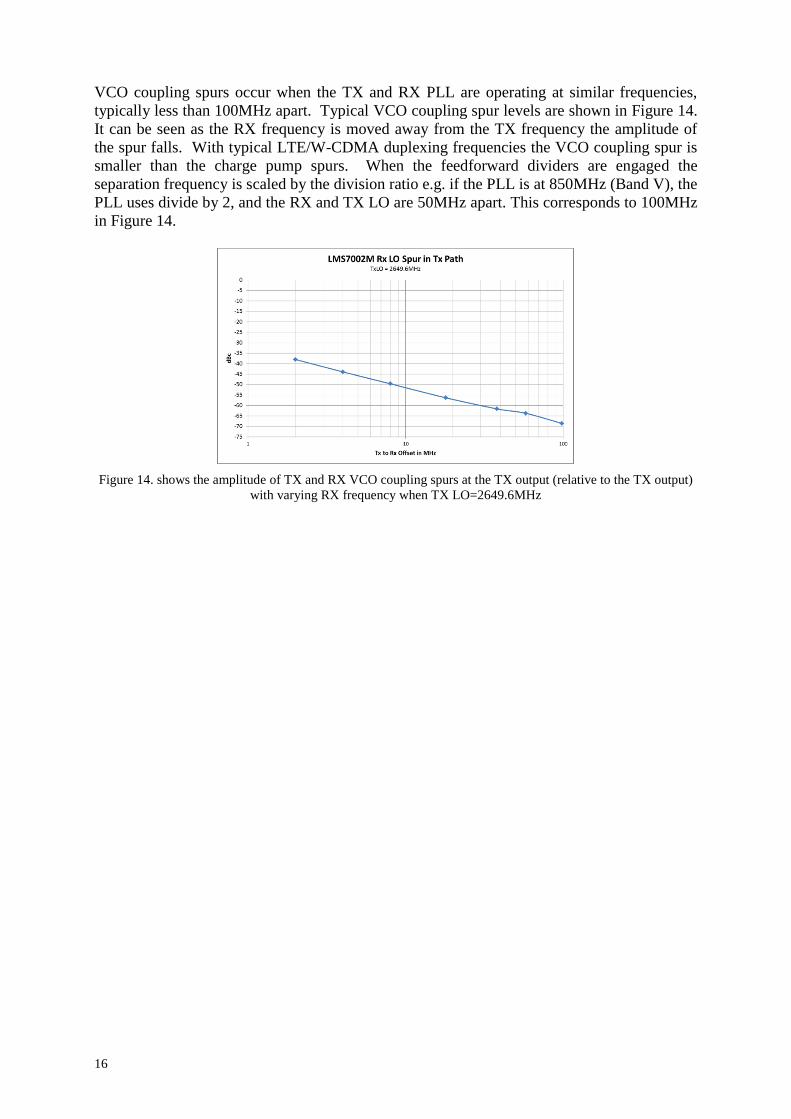
VCO coupling spurs occur when the TX and RX PLL are operating at similar frequencies,
typically less than 100MHz apart. Typical VCO coupling spur levels are shown in Figure 14.
It can be seen as the RX frequency is moved away from the TX frequency the amplitude of
the spur falls. With typical LTE/W-CDMA duplexing frequencies the VCO coupling spur is
smaller than the charge pump spurs. When the feedforward dividers are engaged the
separation frequency is scaled by the division ratio e.g. if the PLL is at 850MHz (Band V), the
PLL uses divide by 2, and the RX and TX LO are 50MHz apart. This corresponds to 100MHz
in Figure 14.
Figure 14. shows the amplitude of TX and RX VCO coupling spurs at the TX output (relative to the TX output)
with varying RX frequency when TX LO=2649.6MHz
17
3 TX Measurements
The transmitter (TX) must modulate the information to be transmitted onto the TX
synthesizer output with almost no degradation of the information quality and with no
interference to users of other frequency bands, especially at nearby frequencies. The quality
of the information being transmitted is usually described by the error vector magnitude
(EVM). EVM includes the effect of phase noise from the synthesizer plateau region as well
as signal to noise ratio, IQ mismatch, group delay mismatch and nonlinearity of the
transmitter and any external power amplifier. The level of interference to users of other
frequency bands is usually described by the adjacent channel power ratio (ACPR) which gives
a measure of the signal to noise ratio available in the next channel. ACPR is degraded by
nonlinearity and noise from the transmitter and external power amplifier and the far out phase
noise from the synthesiser. Additionally the transmitter must maintain performance over a
range of output powers, depending on its application (e.g. amplitude matching of multiple
users in up-links, and maximum output power control in down-links).
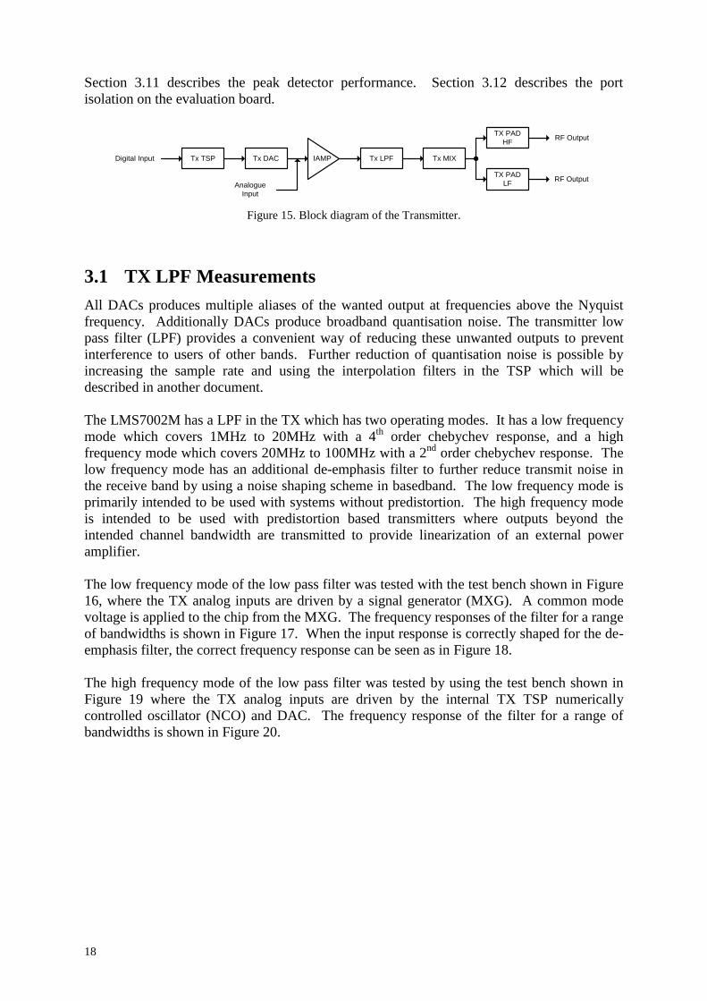
A simplified block diagram of one of the transmitter (TX) channels is shown in Figure 15.
The analog part of the TX consists of a programmable current amplifier (IAMP) to optimally
match the input with the analog IF stage. A programmable analog IF filter (LPF), an RF
mixer, a pair of programmable RF amplifier (PAD) to vary the RF output level. The TX
digital signal processing block (TSP) includes inverse sync correction, digital filtering, dc
offset adjustment for LO leakage cancellation, interpolation for improved signal to noise ratio,
amplitude and phase correction for image rejection and digital upconversion. The
performance of the TSP will be described in another test document.
The following sections describe the measured performance of the transmitter blocks. Section
3.1 describes the frequency response of the transmitter lowpass filters. Section 3.2 describes
the power control of the TX. Sections 3.3 and 3.4 describes optimisation of the TX linearity
for optimum OIP3 and ACPR with W-CDMA respectively. Section 3.5 describes how to use
the internal numerically controlled oscillator (NCO) to optimise linearity. Section 3.6 and 3.7
measure output harmonics and noise respectively. Section 3.8 describes the EVM
performance of the TX with LTE modulation. Section 3.9 describes output power vs
frequency on the evaluation board. Section 3.10 describes the TX noise leakage into the RX.
18
Section 3.11 describes the peak detector performance. Section 3.12 describes the port
isolation on the evaluation board.
Tx TSP Tx DAC IAMP Tx LPF Tx MIX
TX PAD
HF
TX PAD
LF
Digital Input
Analogue
Input
RF Output
RF Output
Figure 15. Block diagram of the Transmitter.
3.1 TX LPF Measurements
All DACs produces multiple aliases of the wanted output at frequencies above the Nyquist
frequency. Additionally DACs produce broadband quantisation noise. The transmitter low
pass filter (LPF) provides a convenient way of reducing these unwanted outputs to prevent
interference to users of other bands. Further reduction of quantisation noise is possible by
increasing the sample rate and using the interpolation filters in the TSP which will be
described in another document.
The LMS7002M has a LPF in the TX which has two operating modes. It has a low frequency
mode which covers 1MHz to 20MHz with a 4th
order chebychev response, and a high
frequency mode which covers 20MHz to 100MHz with a 2nd
order chebychev response. The
low frequency mode has an additional de-emphasis filter to further reduce transmit noise in
the receive band by using a noise shaping scheme in basedband. The low frequency mode is
primarily intended to be used with systems without predistortion. The high frequency mode
is intended to be used with predistortion based transmitters where outputs beyond the
intended channel bandwidth are transmitted to provide linearization of an external power
amplifier.
The low frequency mode of the low pass filter was tested with the test bench shown in Figure
16, where the TX analog inputs are driven by a signal generator (MXG). A common mode
voltage is applied to the chip from the MXG. The frequency responses of the filter for a range
of bandwidths is shown in Figure 17. When the input response is correctly shaped for the de-
emphasis filter, the correct frequency response can be seen as in Figure 18.
The high frequency mode of the low pass filter was tested by using the test bench shown in
Figure 19 where the TX analog inputs are driven by the internal TX TSP numerically
controlled oscillator (NCO) and DAC. The frequency response of the filter for a range of
bandwidths is shown in Figure 20.
19
Figure 16. Test bench used to test TX LPF Low Band
Figure 17. Filter responses of the TX LPF Low Band including de-emphasis pole.
Figure 18. 10MHz Filter responses of the TX LPF Low Band with de-emphasis de-embedded
-35
-30
-25
-20
-15
-10
-5
0
5
0.1 1 10 100
Frequency, MHz
LPF With Pre-Emphasis
20
Figure 19. Test bench used to test TX LPF High Band
Figure 20. Filter responses of the TX LPF High Band
21
3.2 TX RF Gain Measurements
The transmitter TX PAD includes gain control function. This can be found in the TXRF tab of
the GUI. This consists of two parts, the main gain control, and the lineariser gain control.
These are intended to be adjusted together. This is demonstrated using the test bench shown in
Figure 21. The variation of output power and gain step accuracy is shown in Figure 22. The
first 10 steps are 1dB steps, subsequent steps are 2dB steps.
Figure 21. Test bench used to measure TX RF Gain Control
Figure 22. Variation of output power and gain step accuracy with TX RF Gain Control.
22
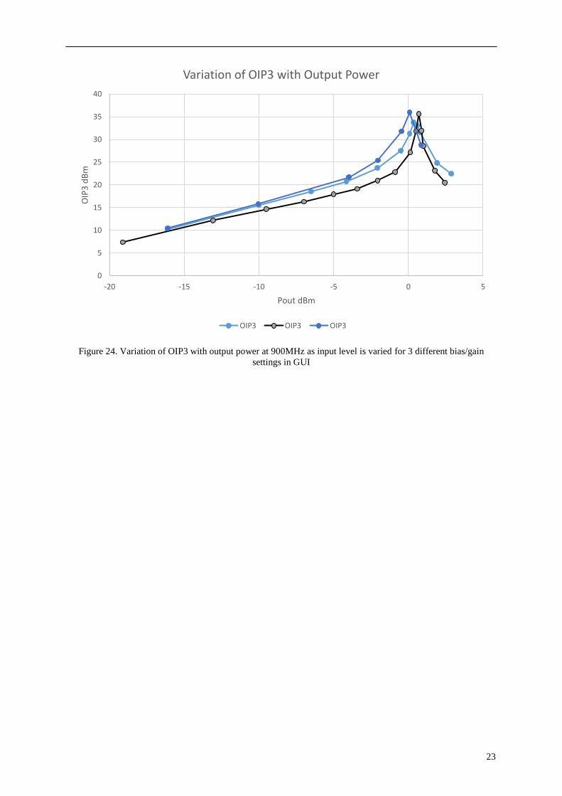
3.3 TX OIP3 Measurements
The TX RF output stage has a linearizer which can be used to optimize OIP3 over a range of
output amplitudes. Using the test set of Figure 23 with a two tone output from the MXG
differential IQ generator. A common mode voltage (0.3V) is applied to the chip from the
MXG. For optimum OIP3 both the TXBB and TXRF have to be carefully aligned to avoid
overloading critical blocks.
First the TXLPF resistors and TXIAMP are set to the required bandwidth (TXBB tab of the
GUI).
Next, the MXG output level and current amplifier IAMP gain (TXBB tab of GUI) are
carefully adjusted to give the lowest IM3 when TXPAD and linearizer gain are both 10dB
backed off from max gain. (This removes the output nonlinearity of the TXPAD, allowing
the TXBB to be optimized for lowest distortion.)
Next, the TXPAD gain is increased to max gain. The RF output power is tuned with the stub
tuner first to achieve maximum output power, and then returned to allow the output power to
fall by 2-3 dB from maximum output power and the tuner carefully adjusted for the position
with lowest distortion at this output power. The distortion is further minimized using the
TXRF tab in the GUI control software using the TXPAD bias currents and gain settings.
The variation of OIP3 at 900MHz is shown in Figure 24 for different gain and bias of the
transmitter.
Table 6. Gain and Bias Settings used to adjust OIP3 maximum.
Pout at OIP3 Peak 0.6 0.7 0
IAMP_GAIN 31 31 31
IAMP_ICT2 3 3 3
TXPAD_GAIN 0 3 3
TXPAD_LINGAIN 3 6 6
TXPAD_ICT 14 15 19
TXPAD_LIN_ICT 31 28 31
Figure 23. Test bench for measuring two tone OIP3.
23
Figure 24. Variation of OIP3 with output power at 900MHz as input level is varied for 3 different bias/gain
settings in GUI
0
5
10
15
20
25
30
35
40
-20 -15 -10 -5 0 5
OIP
3 d
Bm
Pout dBm
Variation of OIP3 with Output Power
OIP3 OIP3 OIP3
24
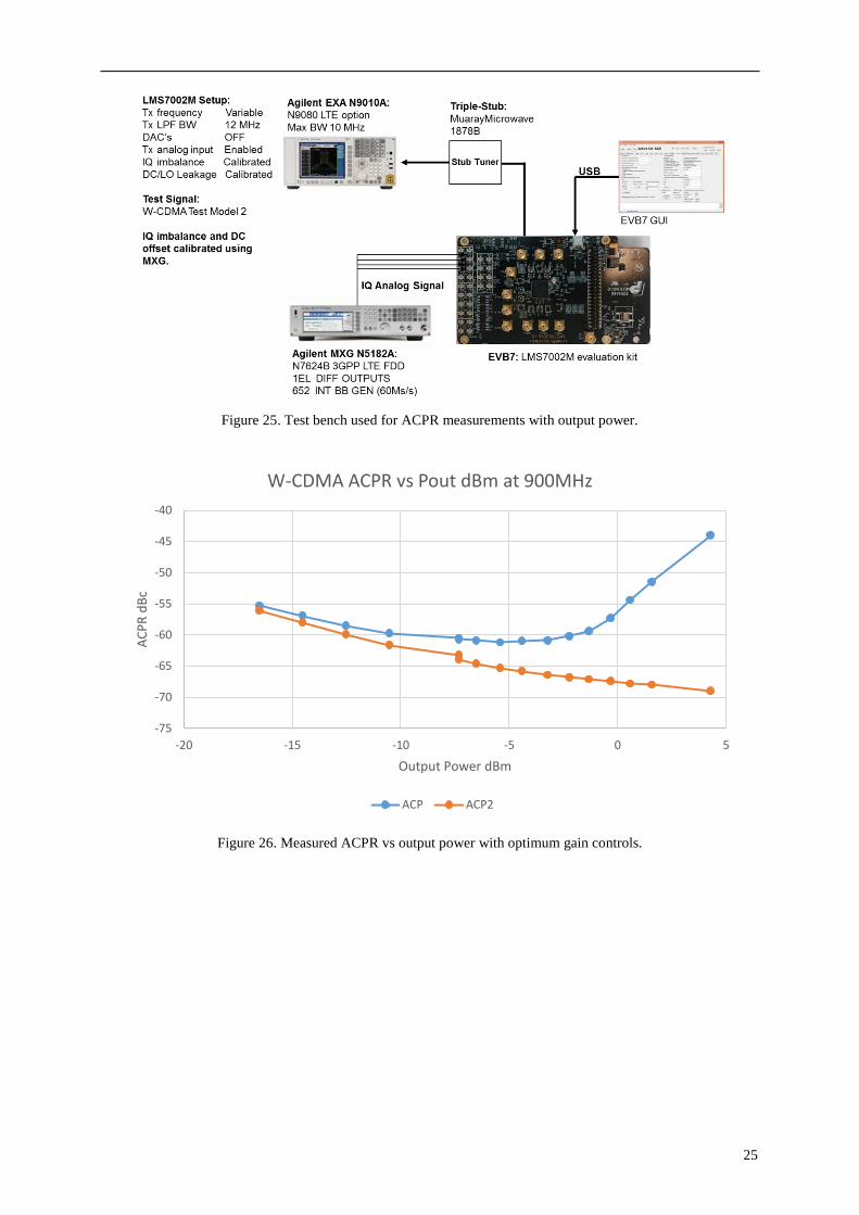
3.4 Optimum TX ACPR Measurements
The TX RF output stage has a linearizer which can be used to optimize ACPR over a range of
output amplitudes using the test set of Figure 25. A W-CDMA signal loaded into the MXG
differential IQ generator. A common mode voltage (0.3V) is applied to the chip from the
MXG. For optimum ACPR both the TXBB and TXRF have to be carefully aligned to avoid
overloading critical blocks.
First the TXLPF resistors and TXIAMP are set to the required bandwidth (TXBB tab of the
GUI).
Next, the MXG output level and current amplifier IAMP gain (TXBB tab of GUI) are
carefully adjusted to give the best ACPR when TXPAD and linearizer gain are both 10dB
backed off from max gain. (this removes the output nonlinearity of the TXPAD, allowing the
TXBB to be optimized for lowest distortion).
Next, the TXPAD gain is increased to max gain. The RF output power is tuned with the stub
tuner first to achieve maximum output power, and then returned to allow the output power to
fall by 2-3 dB and the tuner carefully adjusted for the position with lowest ACPR at this
output power (alternatively the tuner settings from the OIP3 can also be used). The ACPR is
further minimized using the TXRF tab in the GUI control software using the TXPAD bias
currents and gain settings. For most gain steps, the lineariser gain is simply a fixed offset
from the TXPAD gain, the bias currents are held in a constant ratio. For highest output
powers some further adjustment may be needed. The values used here are given in Table 7.
The measured variation of ACPR with RF output power at 900MHz is shown in Figure 26.
Best ACPR is achieved at -5dBm output power.
Further improvements in ACPR measurements could be achieved by using a LNA in front of
the spectrum analyser for low power outputs to reduce the effect of spectrum analyser noise
floor. Same ACPR measurements were done with DAC enabled witch results correspond to
the shown below.
Table 7. Gain and bias settings used for optimum ACPR with output power.
TPAD_Lin 0 0 0 0 3 4 7 8 10 9 11 12 13
TPAD_Main 0 1 2 3 4 5 6 7 8 9 10 11 12
TPAD_casc 3 3 3 3 3 3 3 3 3 3 3 3 3
ICT_LIN 28 28 28 28 28 28 28 28 28 28 28 28 28
ICT_PA 12 12 12 12 12 12 12 12 12 12 12 12 12
NMOS 18 18 18 18 18 18 18 18 18 18 18 18 18
PMOS 24 24 24 24 24 24 24 24 24 24 24 24 24
MXG_VCM 0.31 0.31 0.31 0.31 0.31 0.31 0.31 0.31 0.31 0.31 0.31 0.31 0.31
MXG Scale 6.5 6.5 6.5 6.5 6.5 6.5 6.5 6.5 6.5 6.5 6.5 6.5 6.5
TBB_IAMP_Gain 32 32 32 32 32 32 32 32 32 32 32 32 32
TBB_IAMP_RefBias 3 3 3 3 3 3 3 3 3 3 3 3 3
TBB_IAMP_CalBias 12 12 12 12 12 12 12 12 12 12 12 12 12
TBB_LPF_C 12 12 12 12 12 12 12 12 12 12 12 12 12
TBB_LPF_RLAD 171 171 171 171 171 171 171 171 171 171 171 171 171
TBB_LPF_RRP 135 135 135 135 135 135 135 135 135 135 135 135 135
25
Figure 25. Test bench used for ACPR measurements with output power.
Figure 26. Measured ACPR vs output power with optimum gain controls.
-75
-70
-65
-60
-55
-50
-45
-40
-20 -15 -10 -5 0 5
AC
PR
dB
c
Output Power dBm
W-CDMA ACPR vs Pout dBm at 900MHz
ACP ACP2
26
3.5 Using the TSP NCO for Quick Linearity test
For the best performance from the TX, it is necessary to ensure the TX baseband is not
overloading. The most effective way to set up the TX gains is with a 2 tone signal.
The LMS7002 contains a digital signal processing block (TSP) with a numerically controlled
oscillator (NCO). Normally this digital test signal generates a SSB signal for calibration of
LO leakage and image rejection. But by setting either the I or Q gain in the TSP to 0, it is
possible to use this to generate DSB signal in the mixer, giving a two tone signal at the TX RF
amplifier. This digital test signal can be used to generate test signals to correctly set up the
gain in the TX IF chain.
Depending on the matching and gain set ups, the LMS7002M linearity can either be limited
by the TX baseband blocks (TXBB) or the the TX RF blocks. By setting the TX RF gain to
be approx. 12dB below max gain (or if the TX RF matching is unmatched), the TX RF
nonlinearity can be made very small. This allows the TXBB to be correctly set up. The DAC
has a programmable current output, normally 625uA is selected. By setting the TSP I Q
registers to 7FFF, a full scale waveform can be generated from the DAC. The TX LPF is a
transimpedance stage, converting the DAC output current into a voltage. If the output voltage
is too large, clipping will occur leading to distortion. If this output voltage is too low, the
signal to noise ratio (SNR) will be degraded. The TX current amplifier (IAMP) provides a
means of scaling the DAC output for optimum dynamic range.
Once the TX LPF frequcency response has been set, the IAMP gain can be adjusted for the
inband IM3 to be approximately 60dBc. If the TXRF gain is then changed, the IM3 in dBc
should remain unaltered. Once the TXBB is set up, the TX RF gain can be increased to
measure OIP3. The optional stub tuner could then also be used to match TX RF output for
best compromise of output power and OIP3.
The test bench used for the quick linearity test is shown in Figure 27. In Table 8 we show
typical settings and measured results from setting up the TX IF. The first set of
measurements show how IAMP gain changes IM3. The second set of measurements shows
how changing RF gain does not change IM3 in dBc. The final measurements show how
IAMP gain has to be changed if the TX LPF frequency or band is changed.
Note that the optimum settings shown here are meant for signals with low peak to average
ratio (PAR), such as two tone test signals. OFDM modulation signals, which have a high
PAR, are tolerant to a small amount of clipping of the peaks. One approach is to provide
peak clipping in digital signal processing external to the LMS7002M. Some advance DSP
tools can also give PAR optimized OFDM waveforms. Another approach is to operate the
LMS7002M with a higher IAMP gain than used for the measurements here, and peak clipping
will occur in the analog environment. Error Vector Magnitude (EVM) gives a sensitive
measure of waveform quality and will indicate if digital or analog clipping is too severe
compared to the unclipped waveform.
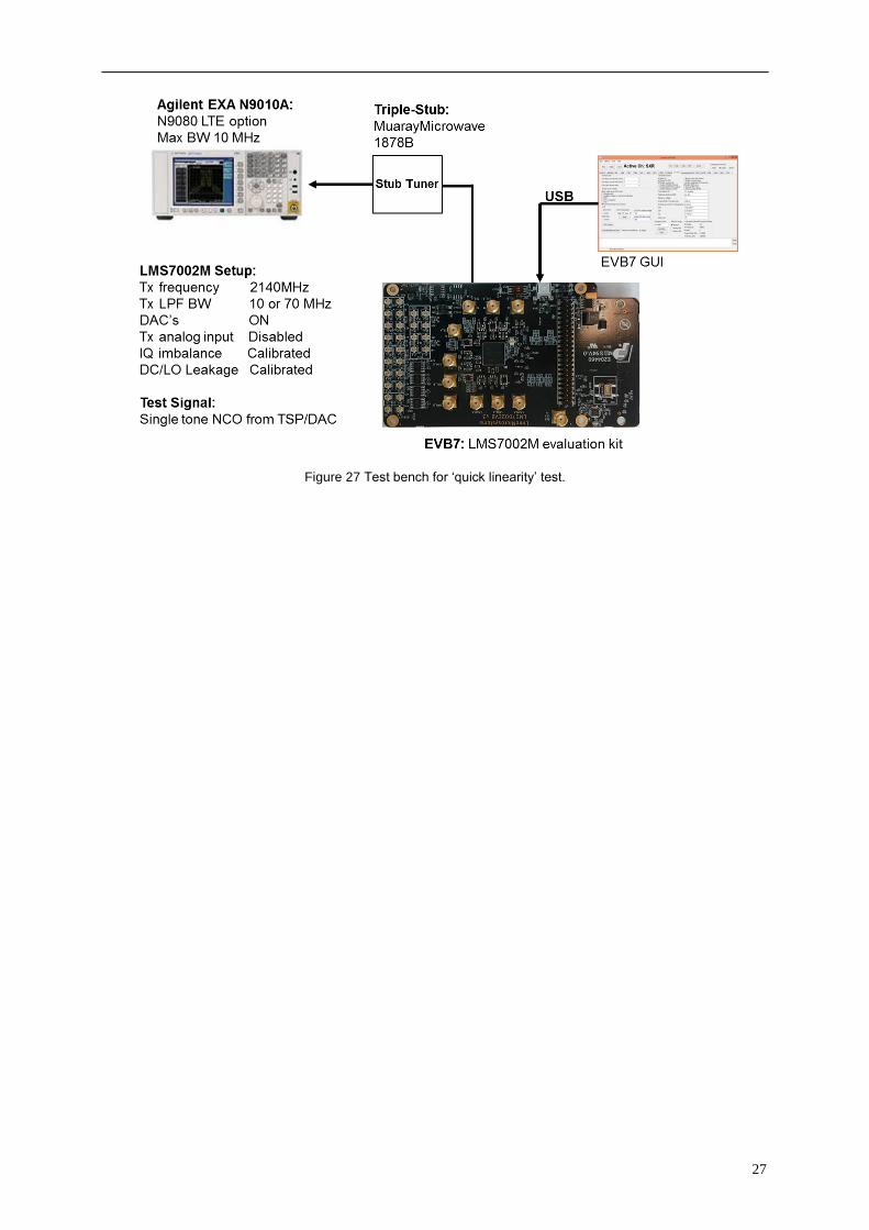
27
Figure 27 Test bench for ‘quick linearity’ test.
28
Table 8 Settings and measured IM3 for ‘quick linearity’ test.
TSP FCW 1 1 1 1 1 1 1 1
TSP Gain Q 2047 2047 2047 2047 2047 2047 2047 2047
TSP Gain I 0 0 0 0 0 0 0 0
TSP DC I -99 -99 -99 -99 -99 -99 -87 -84
TSP DC Q -106 -106 -106 -106 -106 -106 -101 -84
TSP DC_REG I, Q 7FFF 7FFF 7FFF 7FFF 7FFF 7FFF 7FFF 7FFF
TBB IAMP Gain 7 11 15 11 11 11 8 25
TBB IAMP Ref 3 3 3 3 3 3 3 3
TBB IAMP Cascode 12 12 12 12 12 12 12 12
TBB PD_LPFH_biquad y y y y y y y
TBB PD_LPFIAMP
TBB PD__LPFLAD y
TBB PD_LPFS5 y
TBB LPFH 97 97 97 97 97 97 97 97
TBB LPFLAD 171 171 171 171 171 171 85 171
TBB LPFS5 135 135 135 135 135 135 67 135
TBB Cap 12 12 12 12 12 12 12 12
TRF TXPAD lin 0 0 0 0 2 4 0 0
TRF TXPAD gain 2 2 2 2 4 6 2 2
TRF TXPAD Cascode 3 3 3 3 3 3 3 3
TRF Bias gm section 48.3 48.3 48.3 48.3 48.3 48.3 48.3 48.3
TRF Bias lin section 12 12 12 12 12 12 12 12
SXT LO 2140 2140 2140 2140 2140 2140 2140 2140
IM3 2143MHz -78.1 -69.2 -64.0 -69.2 -70.9 -73.6 -69.2 -70.0
USB 2141MHz -16.6 -12.9 -11.3 -12.9 -14.6 -16.6 -12.3 -10.0
LSB 2139MHz -16.4 -12.7 -11.1 -12.7 -14.4 -16.4 -12.0 -9.9
IM3 2137MHz -78.1 -68.5 -62.7 -68.5 -70.0 -72.8 -68.2 -68.7
IM3 dBc -61.5 -56.3 -52.7 -56.3 -56.3 -57.0 -56.9 -60.0
IM3 dBc -61.7 -55.8 -51.6 -55.8 -55.6 -56.4 -56.2 -58.8
3.6 TX Output Harmonics
The transmitter produces harmonics of the wanted output. The even harmonic levels are low
due to the use of differential outputs, which reduces filtering requirements.
The transmitter harmonic responses are measured with the test set shown in Figure 28. The
NCO is used to produce a 1-tone test signal. The stub tuner is used to ensure the output
power is the maximum value possible at the wanted frequency. The largest spur at each
harmonic frequency is measured. Measuured harmonic outputs at maximum TX RF gain are
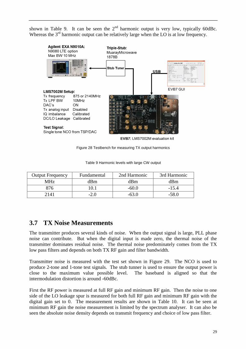
29
shown in Table 9. It can be seen the 2nd
harmonic output is very low, typically 60dBc.
Whereas the 3rd
harmonic output can be relatively large when the LO is at low frequency.
Figure 28 Testbench for measuring TX output harmonics
Table 9 Harmonic levels with large CW output
Output Frequency Fundamental 2nd Harmonic 3rd Harmonic
MHz dBm dBm dBm
876 10.1 -60.0 -15.4
2141 -2.0 -63.0 -58.0
3.7 TX Noise Measurements
The transmitter produces several kinds of noise. When the output signal is large, PLL phase
noise can contribute. But when the digital input is made zero, the thermal noise of the
transmitter dominates residual noise. The thermal noise predominately comes from the TX
low pass filters and depends on both TX RF gain and filter bandwidth.
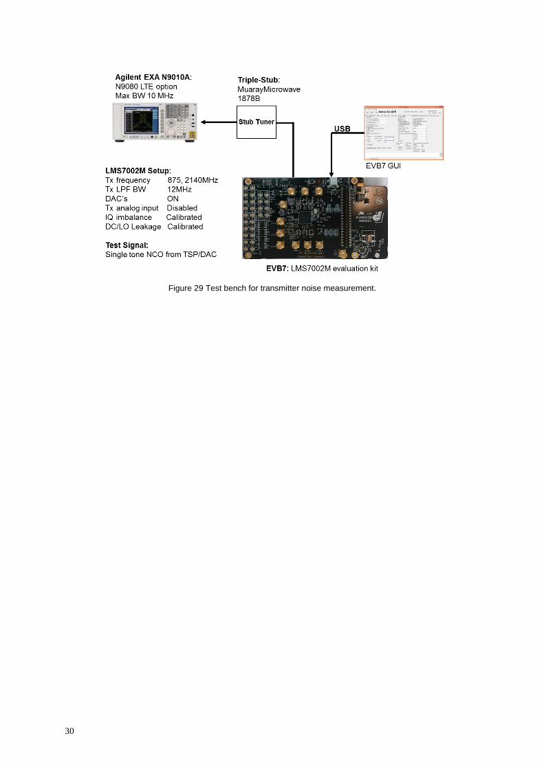
Transmitter noise is measured with the test set shown in Figure 29. The NCO is used to
produce 2-tone and 1-tone test signals. The stub tunner is used to ensure the output power is
close to the maximum value possible level. The baseband is aligned so that the
intermodulation distortion is around -60dBc.
First the RF power is measured at full RF gain and minimum RF gain. Then the noise to one
side of the LO leakage spur is measured for both full RF gain and minimum RF gain with the
digital gain set to 0. The measurement results are shown in Table 10. It can be seen at
minimum RF gain the noise measurement is limited by the spectrum analyser. It can also be
seen the absolute noise density depends on transmit frequency and choice of low pass filter.
30
Figure 29 Test bench for transmitter noise measurement.
31
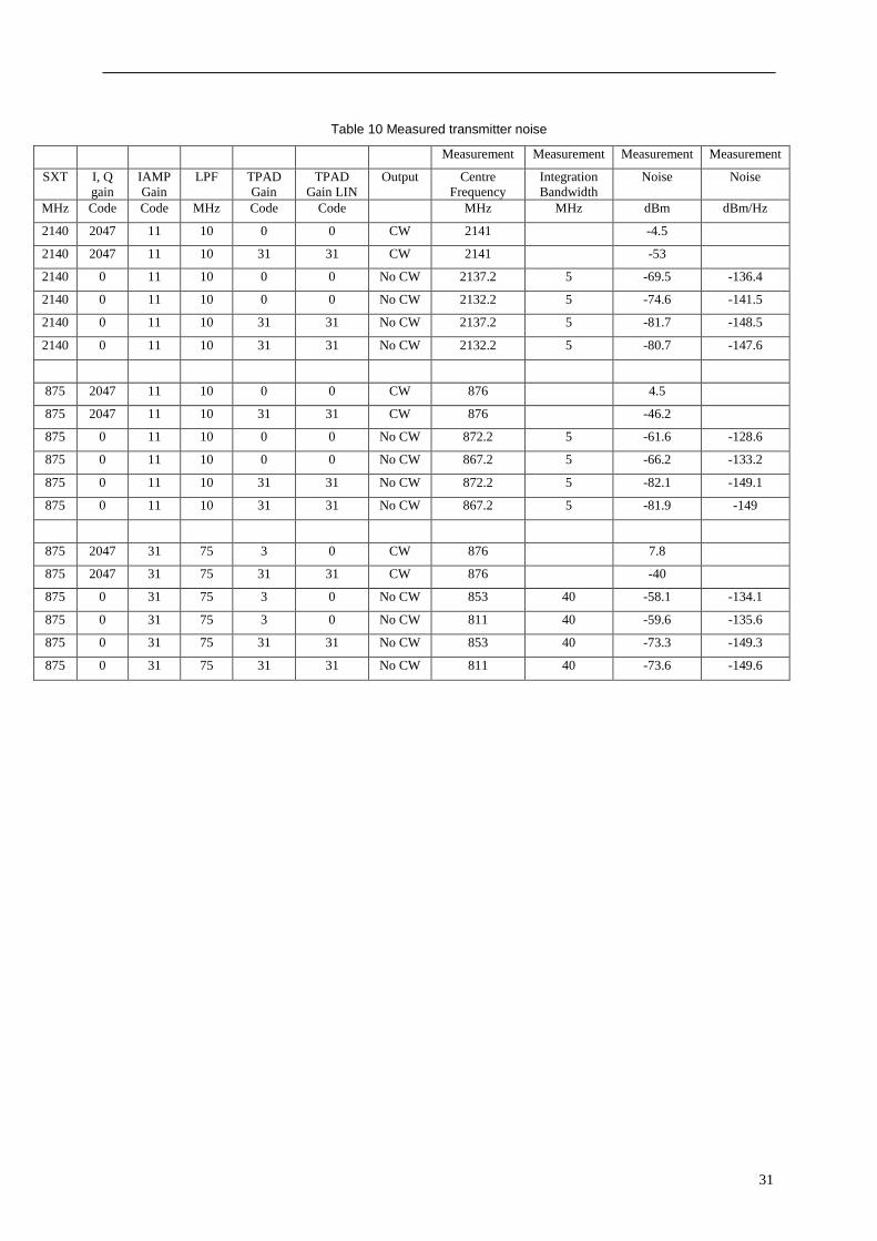
Table 10 Measured transmitter noise
Measurement Measurement Measurement Measurement
SXT I, Q
gain
IAMP
Gain
LPF TPAD
Gain
TPAD
Gain LIN
Output Centre
Frequency
Integration
Bandwidth
Noise Noise
MHz Code Code MHz Code Code MHz MHz dBm dBm/Hz
2140 2047 11 10 0 0 CW 2141 -4.5
2140 2047 11 10 31 31 CW 2141 -53
2140 0 11 10 0 0 No CW 2137.2 5 -69.5 -136.4
2140 0 11 10 0 0 No CW 2132.2 5 -74.6 -141.5
2140 0 11 10 31 31 No CW 2137.2 5 -81.7 -148.5
2140 0 11 10 31 31 No CW 2132.2 5 -80.7 -147.6
875 2047 11 10 0 0 CW 876 4.5
875 2047 11 10 31 31 CW 876 -46.2
875 0 11 10 0 0 No CW 872.2 5 -61.6 -128.6
875 0 11 10 0 0 No CW 867.2 5 -66.2 -133.2
875 0 11 10 31 31 No CW 872.2 5 -82.1 -149.1
875 0 11 10 31 31 No CW 867.2 5 -81.9 -149
875 2047 31 75 3 0 CW 876 7.8
875 2047 31 75 31 31 CW 876 -40
875 0 31 75 3 0 No CW 853 40 -58.1 -134.1
875 0 31 75 3 0 No CW 811 40 -59.6 -135.6
875 0 31 75 31 31 No CW 853 40 -73.3 -149.3
875 0 31 75 31 31 No CW 811 40 -73.6 -149.6
32
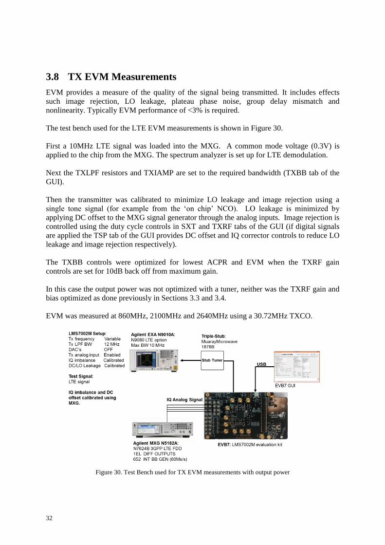
3.8 TX EVM Measurements
EVM provides a measure of the quality of the signal being transmitted. It includes effects
such image rejection, LO leakage, plateau phase noise, group delay mismatch and
nonlinearity. Typically EVM performance of <3% is required.
The test bench used for the LTE EVM measurements is shown in Figure 30.
First a 10MHz LTE signal was loaded into the MXG. A common mode voltage (0.3V) is
applied to the chip from the MXG. The spectrum analyzer is set up for LTE demodulation.
Next the TXLPF resistors and TXIAMP are set to the required bandwidth (TXBB tab of the
GUI).
Then the transmitter was calibrated to minimize LO leakage and image rejection using a
single tone signal (for example from the ‘on chip’ NCO). LO leakage is minimized by
applying DC offset to the MXG signal generator through the analog inputs. Image rejection is
controlled using the duty cycle controls in SXT and TXRF tabs of the GUI (if digital signals
are applied the TSP tab of the GUI provides DC offset and IQ corrector controls to reduce LO
leakage and image rejection respectively).
The TXBB controls were optimized for lowest ACPR and EVM when the TXRF gain
controls are set for 10dB back off from maximum gain.
In this case the output power was not optimized with a tuner, neither was the TXRF gain and
bias optimized as done previously in Sections 3.3 and 3.4.
EVM was measured at 860MHz, 2100MHz and 2640MHz using a 30.72MHz TXCO.
Figure 30. Test Bench used for TX EVM measurements with output power
33
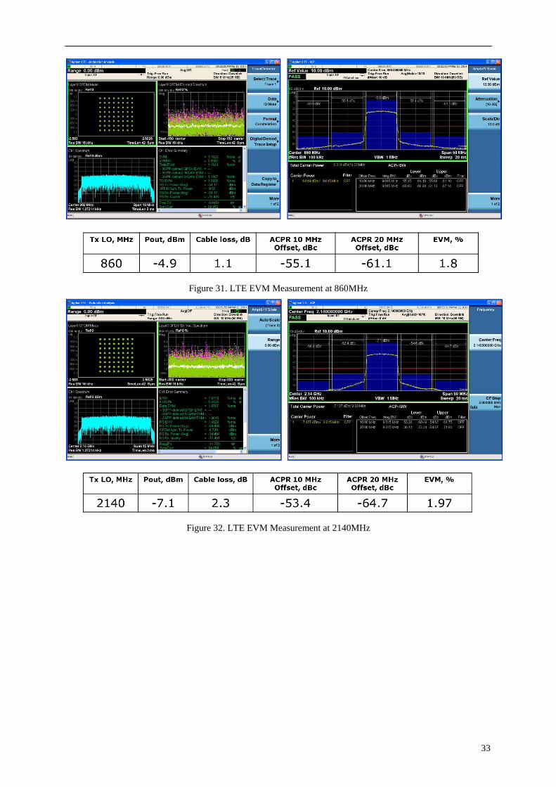
Figure 31. LTE EVM Measurement at 860MHz
Figure 32. LTE EVM Measurement at 2140MHz
34
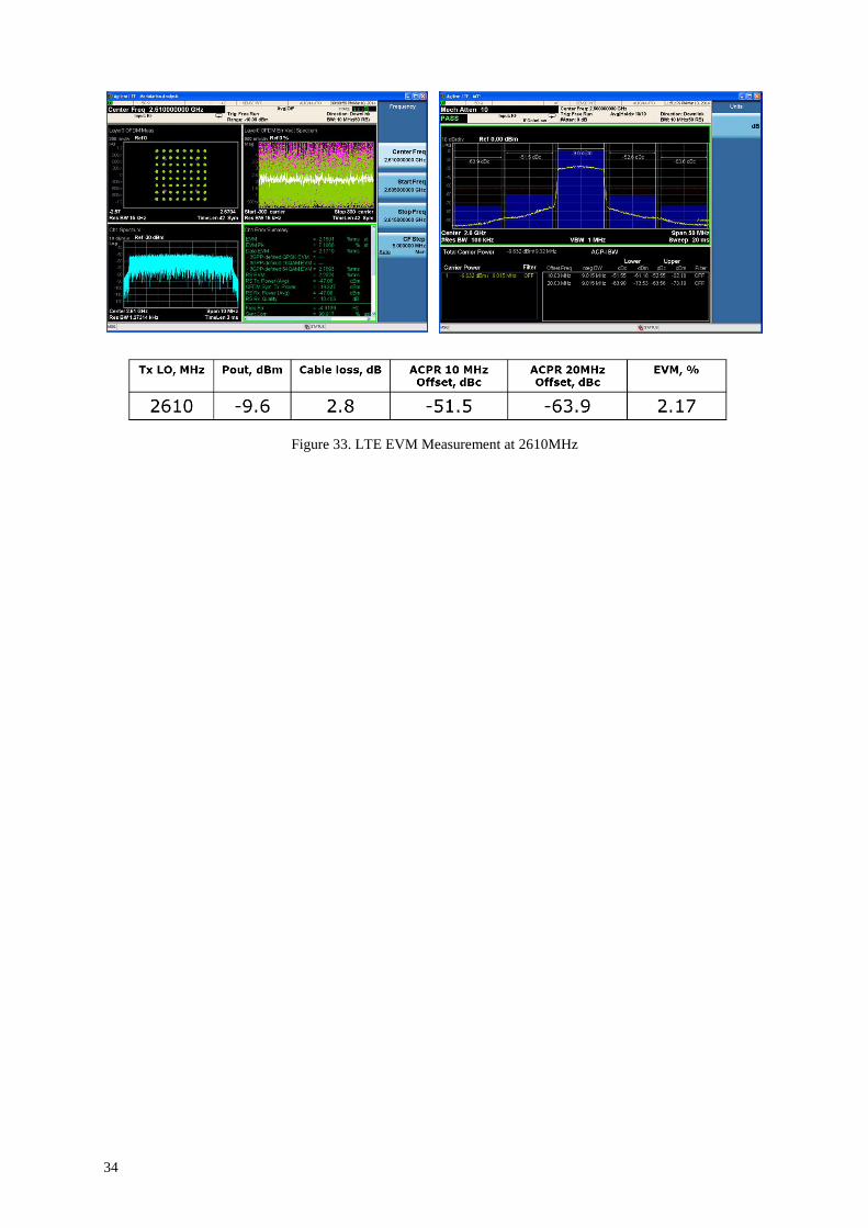
Figure 33. LTE EVM Measurement at 2610MHz
35
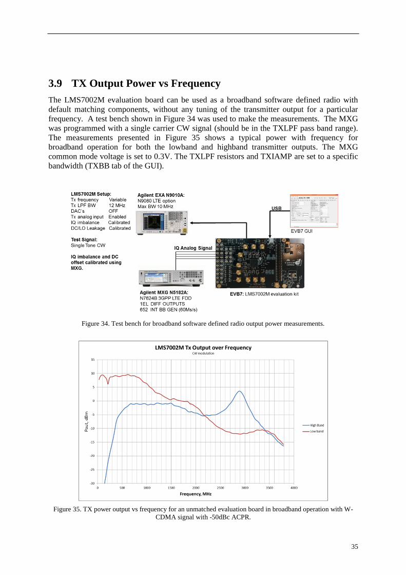
3.9 TX Output Power vs Frequency
The LMS7002M evaluation board can be used as a broadband software defined radio with
default matching components, without any tuning of the transmitter output for a particular
frequency. A test bench shown in Figure 34 was used to make the measurements. The MXG
was programmed with a single carrier CW signal (should be in the TXLPF pass band range).
The measurements presented in Figure 35 shows a typical power with frequency for
broadband operation for both the lowband and highband transmitter outputs. The MXG
common mode voltage is set to 0.3V. The TXLPF resistors and TXIAMP are set to a specific
bandwidth (TXBB tab of the GUI).
Figure 34. Test bench for broadband software defined radio output power measurements.
Figure 35. TX power output vs frequency for an unmatched evaluation board in broadband operation with W-
CDMA signal with -50dBc ACPR.
36
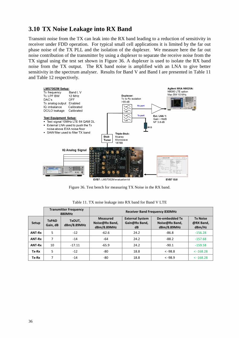
3.10 TX Noise Leakage into RX Band
Transmit noise from the TX can leak into the RX band leading to a reduction of sensitivity in
receiver under FDD operation. For typical small cell applications it is limited by the far out
phase noise of the TX PLL and the isolation of the duplexer. We measure here the far out
noise contribution of the transmitter by using a duplexer to separate the receive noise from the
TX signal using the test set shown in Figure 36. A duplexer is used to isolate the RX band
noise from the TX output. The RX band noise is amplified with an LNA to give better
sensitivity in the spectrum analyser. Results for Band V and Band I are presented in Table 11
and Table 12 respectively.
Figure 36. Test bench for measuring TX Noise in the RX band.
Table 11. TX noise leakage into RX band for Band V LTE
Transmitter Frequency 880MHz
Receiver Band Frequency 830MHz
Setup TxPAD
Gain, dB TxOUT,
dBm/8.89MHz
Measured Noise@Rx Band, dBm/8.89MHz
External System Gain@Rx Band,
dB
De-embedded Tx Noise@Rx Band, dBm/8.89MHz
Tx Noise @RX Band,
dBm/Hz
ANT-Rx 5 -12 -62.6 24.2 -86.8 -156.28
ANT-Rx 7 -14 -64 24.2 -88.2 -157.68
ANT-Rx 10 -17.11 -65.9 24.2 -90.1 -159.58
Tx-Rx 5 -12 -80 18.8 < -98.8 < -168.28
Tx-Rx 7 -14 -80 18.8 < -98.9 < -168.28
37
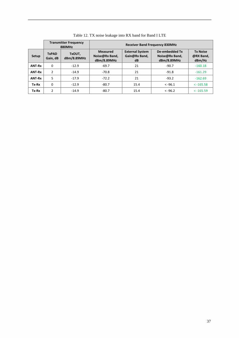
Table 12. TX noise leakage into RX band for Band I LTE
Transmitter Frequency 880MHz
Receiver Band Frequency 830MHz
Setup TxPAD
Gain, dB TxOUT,
dBm/8.89MHz
Measured Noise@Rx Band, dBm/8.89MHz
External System Gain@Rx Band,
dB
De-embedded Tx Noise@Rx Band, dBm/8.89MHz
Tx Noise @RX Band,
dBm/Hz
ANT-Rx 0 -12.9 -69.7 21 -90.7 -160.18
ANT-Rx 2 -14.9 -70.8 21 -91.8 -161.29
ANT-Rx 5 -17.9 -72.2 21 -93.2 -162.69
Tx-Rx 0 -12.9 -80.7 15.4 < -96.1 < -165.58
Tx-Rx 2 -14.9 -80.7 15.4 < -96.2 < -165.59
38
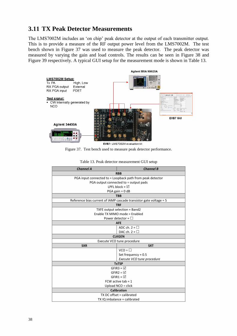
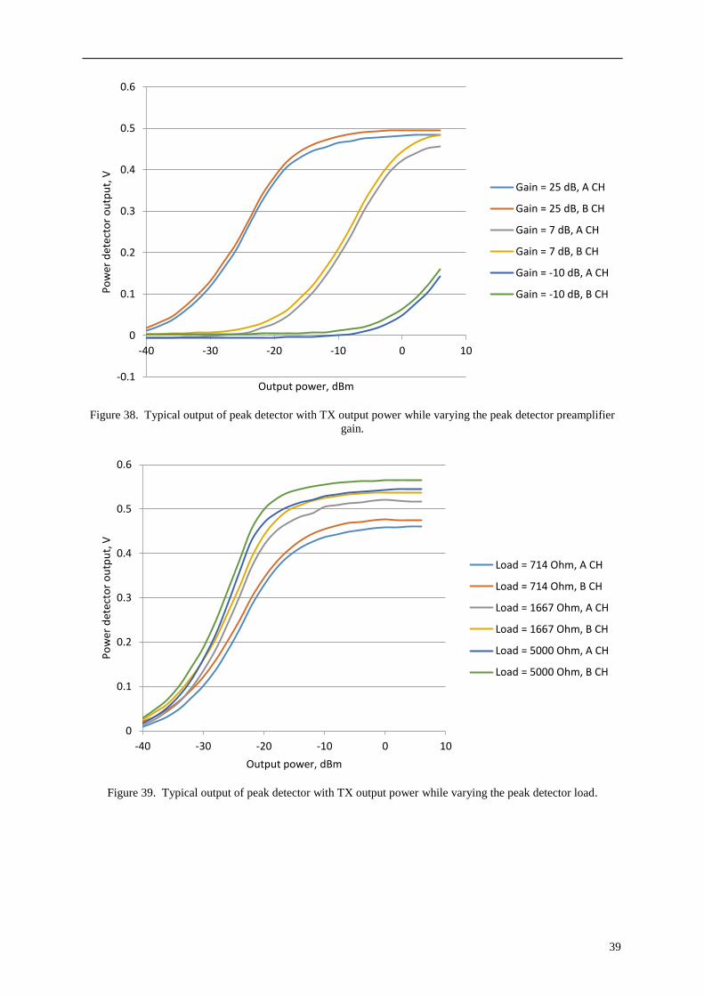
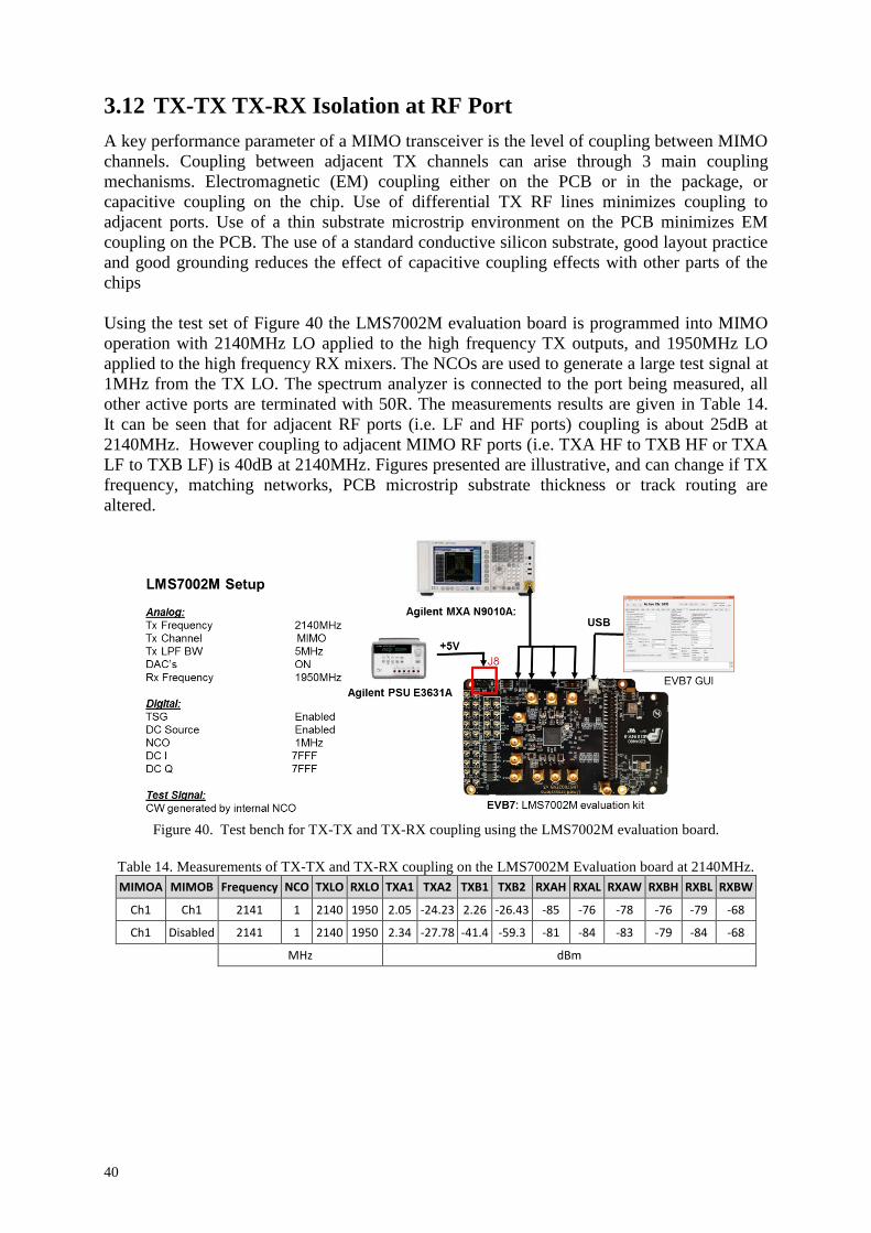
3.11 TX Peak Detector Measurements
The LMS7002M includes an ‘on chip’ peak detector at the output of each transmitter output.
This is to provide a measure of the RF output power level from the LMS7002M. The test
bench shown in Figure 37 was used to measure the peak detector. The peak detector was
measured by varying the gain and load controls. The results can be seen in Figure 38 and
Figure 39 respectively. A typical GUI setup for the measurement mode is shown in Table 13.
Figure 37. Test bench used to measure peak detector performance.
Table 13. Peak detector measurement GUI setup
Channel A Channel B
RBB
PGA input connected to = Loopback path from peak detector PGA output connected to = output pads
LPFL block = PGA gain = 0 dB
TBB
Reference bias current of IAMP cascade transistor gate voltage = 5
TRF
TXFE output selection = Band2 Enable TX MIMO mode = Enabled
Power detector =
AFE
ADC ch. 2 = DAC ch. 2 =
CLKGEN
Execute VCO tune procedure
SXR SXT
VCO = Set frequency = 0.5 Execute VCO tune procedure
TxTSP
GFIR3 = GFIR2 = GFIR1 =
FCW active tab = 1 Upload NCO = click
Calibration
TX DC offset = calibrated TX IQ imbalance = calibrated
39
Figure 38. Typical output of peak detector with TX output power while varying the peak detector preamplifier
gain.
Figure 39. Typical output of peak detector with TX output power while varying the peak detector load.
-0.1
0
0.1
0.2
0.3
0.4
0.5
0.6
-40 -30 -20 -10 0 10
Po
wer
det
ecto
r o
utp
ut,
V
Output power, dBm
Gain = 25 dB, A CH
Gain = 25 dB, B CH
Gain = 7 dB, A CH
Gain = 7 dB, B CH
Gain = -10 dB, A CH
Gain = -10 dB, B CH
0
0.1
0.2
0.3
0.4
0.5
0.6
-40 -30 -20 -10 0 10
Po
wer
det
ecto
r o
utp
ut,
V
Output power, dBm
Load = 714 Ohm, A CH
Load = 714 Ohm, B CH
Load = 1667 Ohm, A CH
Load = 1667 Ohm, B CH
Load = 5000 Ohm, A CH
Load = 5000 Ohm, B CH
40
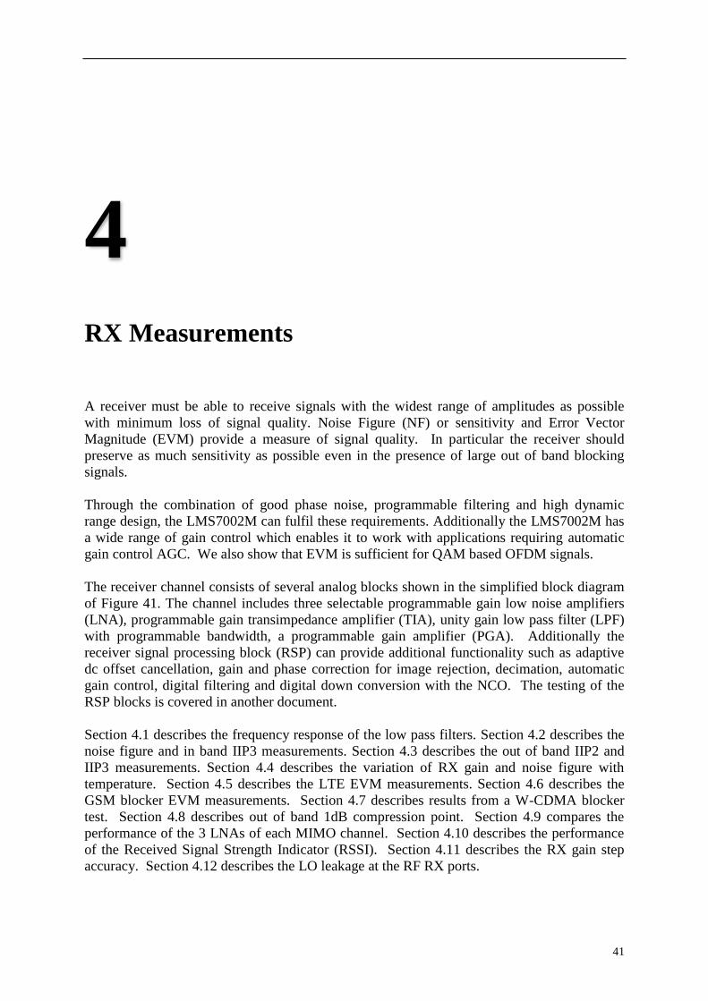
3.12 TX-TX TX-RX Isolation at RF Port
A key performance parameter of a MIMO transceiver is the level of coupling between MIMO
channels. Coupling between adjacent TX channels can arise through 3 main coupling
mechanisms. Electromagnetic (EM) coupling either on the PCB or in the package, or
capacitive coupling on the chip. Use of differential TX RF lines minimizes coupling to
adjacent ports. Use of a thin substrate microstrip environment on the PCB minimizes EM
coupling on the PCB. The use of a standard conductive silicon substrate, good layout practice
and good grounding reduces the effect of capacitive coupling effects with other parts of the
chips
Using the test set of Figure 40 the LMS7002M evaluation board is programmed into MIMO
operation with 2140MHz LO applied to the high frequency TX outputs, and 1950MHz LO
applied to the high frequency RX mixers. The NCOs are used to generate a large test signal at
1MHz from the TX LO. The spectrum analyzer is connected to the port being measured, all
other active ports are terminated with 50R. The measurements results are given in Table 14.
It can be seen that for adjacent RF ports (i.e. LF and HF ports) coupling is about 25dB at
2140MHz. However coupling to adjacent MIMO RF ports (i.e. TXA HF to TXB HF or TXA
LF to TXB LF) is 40dB at 2140MHz. Figures presented are illustrative, and can change if TX
frequency, matching networks, PCB microstrip substrate thickness or track routing are
altered.
Figure 40. Test bench for TX-TX and TX-RX coupling using the LMS7002M evaluation board.
Table 14. Measurements of TX-TX and TX-RX coupling on the LMS7002M Evaluation board at 2140MHz.
MIMOA MIMOB Frequency NCO TXLO RXLO TXA1 TXA2 TXB1 TXB2 RXAH RXAL RXAW RXBH RXBL RXBW
Ch1 Ch1 2141 1 2140 1950 2.05 -24.23 2.26 -26.43 -85 -76 -78 -76 -79 -68
Ch1 Disabled 2141 1 2140 1950 2.34 -27.78 -41.4 -59.3 -81 -84 -83 -79 -84 -68
MHz dBm
41
4 RX Measurements
A receiver must be able to receive signals with the widest range of amplitudes as possible
with minimum loss of signal quality. Noise Figure (NF) or sensitivity and Error Vector
Magnitude (EVM) provide a measure of signal quality. In particular the receiver should
preserve as much sensitivity as possible even in the presence of large out of band blocking
signals.
Through the combination of good phase noise, programmable filtering and high dynamic
range design, the LMS7002M can fulfil these requirements. Additionally the LMS7002M has
a wide range of gain control which enables it to work with applications requiring automatic
gain control AGC. We also show that EVM is sufficient for QAM based OFDM signals.
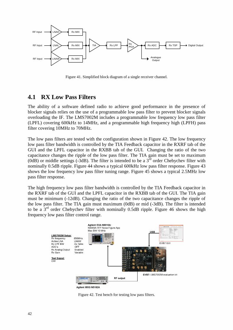
The receiver channel consists of several analog blocks shown in the simplified block diagram
of Figure 41. The channel includes three selectable programmable gain low noise amplifiers
(LNA), programmable gain transimpedance amplifier (TIA), unity gain low pass filter (LPF)
with programmable bandwidth, a programmable gain amplifier (PGA). Additionally the
receiver signal processing block (RSP) can provide additional functionality such as adaptive
dc offset cancellation, gain and phase correction for image rejection, decimation, automatic
gain control, digital filtering and digital down conversion with the NCO. The testing of the
RSP blocks is covered in another document.
Section 4.1 describes the frequency response of the low pass filters. Section 4.2 describes the
noise figure and in band IIP3 measurements. Section 4.3 describes the out of band IIP2 and
IIP3 measurements. Section 4.4 describes the variation of RX gain and noise figure with
temperature. Section 4.5 describes the LTE EVM measurements. Section 4.6 describes the
GSM blocker EVM measurements. Section 4.7 describes results from a W-CDMA blocker
test. Section 4.8 describes out of band 1dB compression point. Section 4.9 compares the
performance of the 3 LNAs of each MIMO channel. Section 4.10 describes the performance
of the Received Signal Strength Indicator (RSSI). Section 4.11 describes the RX gain step
accuracy. Section 4.12 describes the LO leakage at the RF RX ports.
42
LNAH
LNAL
LNAW
Rx MIX
Rx MIX
Rx MIX
TIA Rx LPFRx
PGARx ADC Rx TSP
RF Input
RF Input
RF Input
Digital Output
Analogue
Output
Figure 41. Simplified block diagram of a single receiver channel.
4.1 RX Low Pass Filters
The ability of a software defined radio to achieve good performance in the presence of
blocker signals relies on the use of a programmable low pass filter to prevent blocker signals
overloading the IF. The LMS7002M includes a programmable low frequency low pass filter
(LPFL) covering 600kHz to 14MHz, and a programmable high frequency high (LPFH) pass
filter covering 10MHz to 70MHz.
The low pass filters are tested with the configuration shown in Figure 42. The low frequency
low pass filter bandwidth is controlled by the TIA Feedback capacitor in the RXRF tab of the
GUI and the LPFL capacitor in the RXBB tab of the GUI. Changing the ratio of the two
capacitance changes the ripple of the low pass filter. The TIA gain must be set to maximum
(0dB) or middle settings (-3dB). The filter is intended to be a 3rd
order Chebychev filter with
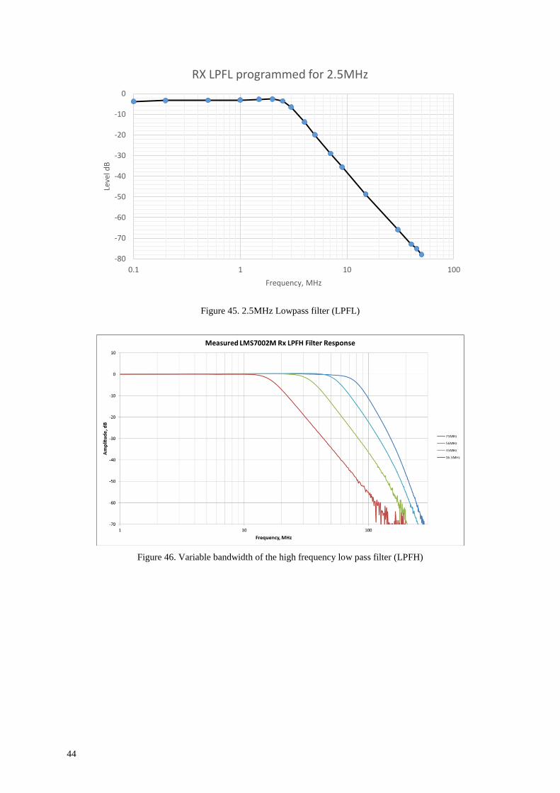
nominally 0.5dB ripple. Figure 44 shows a typical 600kHz low pass filter response. Figure 43
shows the low frequency low pass filter tuning range. Figure 45 shows a typical 2.5MHz low
pass filter response.
The high frequency low pass filter bandwidth is controlled by the TIA Feedback capacitor in
the RXRF tab of the GUI and the LPFL capacitor in the RXBB tab of the GUI. The TIA gain
must be minimum (-12dB). Changing the ratio of the two capacitance changes the ripple of
the low pass filter. The TIA gain must maximum (0dB) or mid (-3dB). The filter is intended
to be a 3rd
order Chebychev filter with nominally 0.5dB ripple. Figure 46 shows the high
frequency low pass filter control range.
Figure 42. Test bench for testing low pass filters.
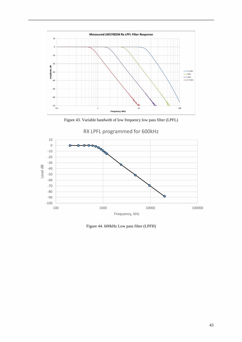
43
Figure 43. Variable bandwith of low frequency low pass filter (LPFL)
Figure 44. 600kHz Low pass filter (LPFH)
-100
-90
-80
-70
-60
-50
-40
-30
-20
-10
0
10
100 1000 10000 100000
Leve
l dB
Frequency, kHz
RX LPFL programmed for 600kHz
44
Figure 45. 2.5MHz Lowpass filter (LPFL)
Figure 46. Variable bandwidth of the high frequency low pass filter (LPFH)
-80
-70
-60
-50
-40
-30
-20
-10
0
0.1 1 10 100
Leve
l dB
Frequency, MHz
RX LPFL programmed for 2.5MHz
45
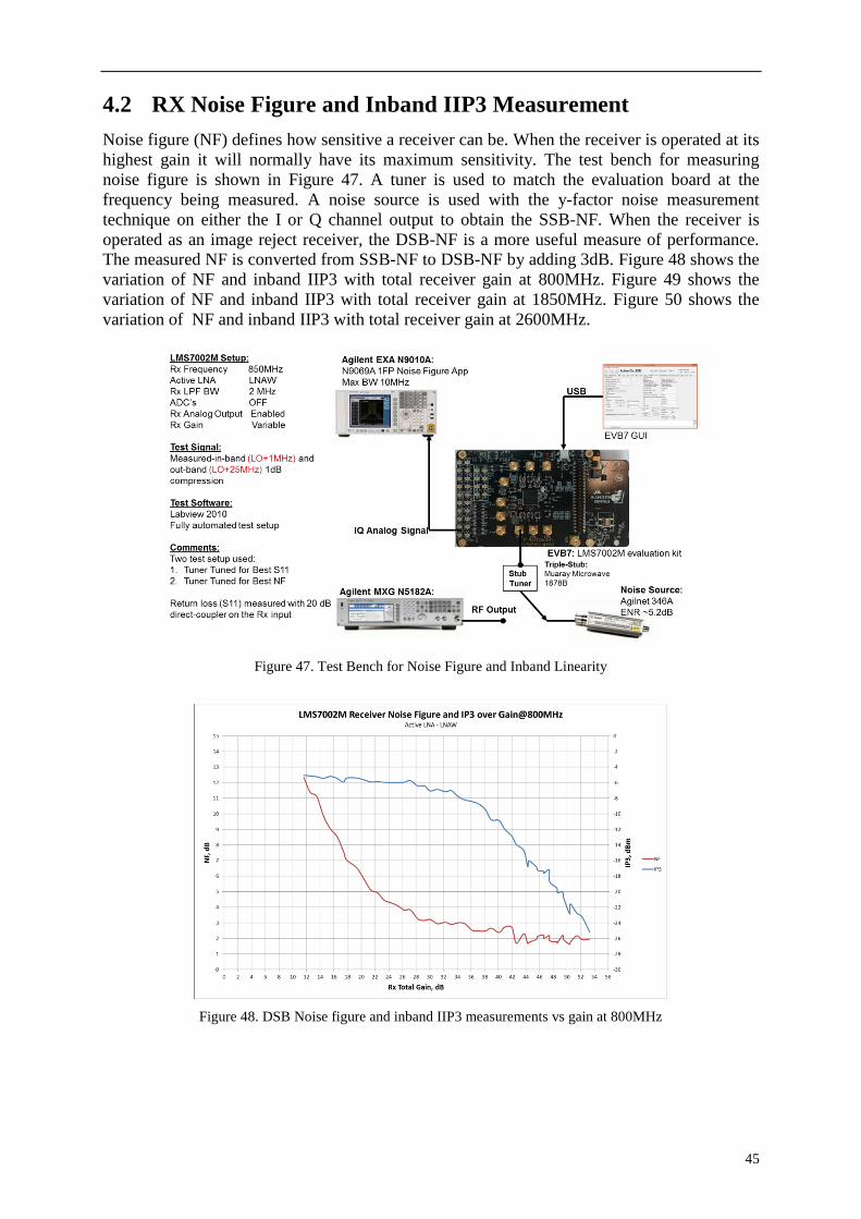
4.2 RX Noise Figure and Inband IIP3 Measurement
Noise figure (NF) defines how sensitive a receiver can be. When the receiver is operated at its
highest gain it will normally have its maximum sensitivity. The test bench for measuring
noise figure is shown in Figure 47. A tuner is used to match the evaluation board at the
frequency being measured. A noise source is used with the y-factor noise measurement
technique on either the I or Q channel output to obtain the SSB-NF. When the receiver is
operated as an image reject receiver, the DSB-NF is a more useful measure of performance.
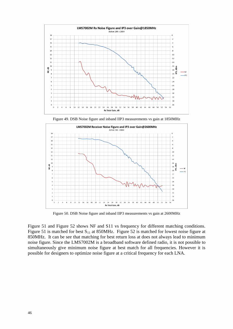
The measured NF is converted from SSB-NF to DSB-NF by adding 3dB. Figure 48 shows the
variation of NF and inband IIP3 with total receiver gain at 800MHz. Figure 49 shows the
variation of NF and inband IIP3 with total receiver gain at 1850MHz. Figure 50 shows the
variation of NF and inband IIP3 with total receiver gain at 2600MHz.
Figure 47. Test Bench for Noise Figure and Inband Linearity
Figure 48. DSB Noise figure and inband IIP3 measurements vs gain at 800MHz
46
Figure 49. DSB Noise figure and inband IIP3 measurements vs gain at 1850MHz
Figure 50. DSB Noise figure and inband IIP3 measurements vs gain at 2600MHz
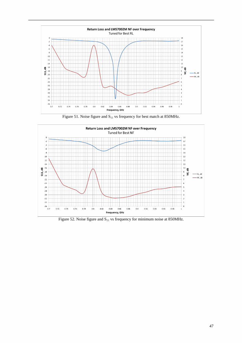
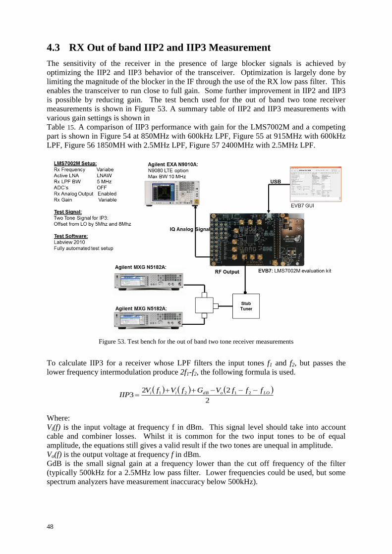
Figure 51 and Figure 52 shows NF and S11 vs frequency for different matching conditions.
Figure 51 is matched for best S11 at 850MHz. Figure 52 is matched for lowest noise figure at
850MHz. It can be see that matching for best return loss at does not always lead to minimum
noise figure. Since the LMS7002M is a broadband software defined radio, it is not possible to
simultaneously give minimum noise figure at best match for all frequencies. However it is
possible for designers to optimize noise figure at a critical frequency for each LNA.
47
Figure 51. Noise figure and S11 vs frequency for best match at 850MHz.
Figure 52. Noise figure and S11 vs frequency for minimum noise at 850MHz.
48
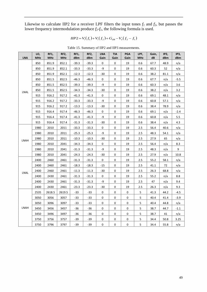
4.3 RX Out of band IIP2 and IIP3 Measurement
The sensitivity of the receiver in the presence of large blocker signals is achieved by
optimizing the IIP2 and IIP3 behavior of the transceiver. Optimization is largely done by
limiting the magnitude of the blocker in the IF through the use of the RX low pass filter. This
enables the transceiver to run close to full gain. Some further improvement in IIP2 and IIP3
is possible by reducing gain. The test bench used for the out of band two tone receiver
measurements is shown in Figure 53. A summary table of IIP2 and IIP3 measurements with
various gain settings is shown in
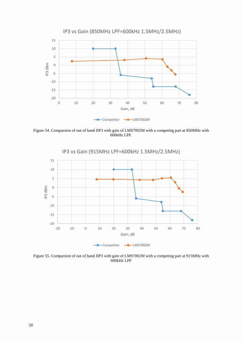
Table 15. A comparison of IIP3 performance with gain for the LMS7002M and a competing
part is shown in Figure 54 at 850MHz with 600kHz LPF, Figure 55 at 915MHz with 600kHz
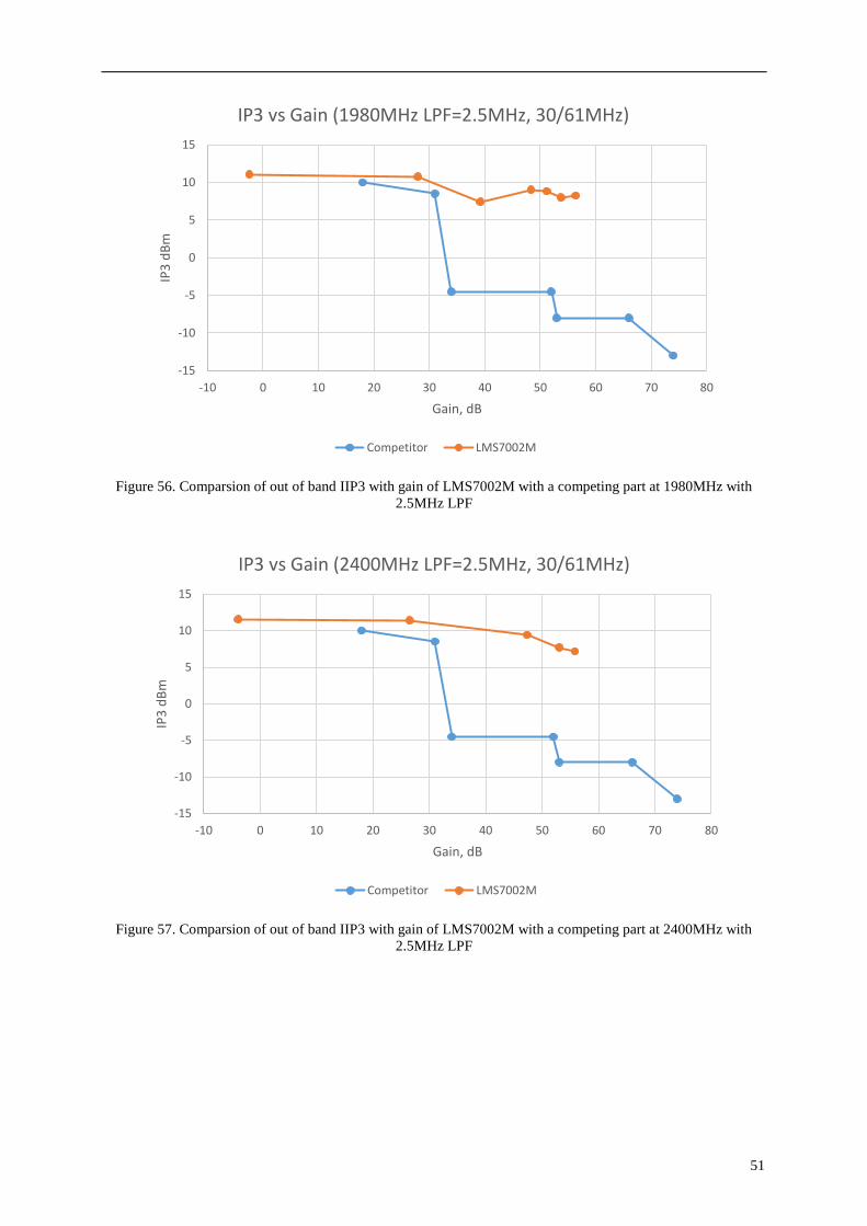
LPF, Figure 56 1850MH with 2.5MHz LPF, Figure 57 2400MHz with 2.5MHz LPF.
Figure 53. Test bench for the out of band two tone receiver measurements
To calculate IIP3 for a receiver whose LPF filters the input tones f1 and f2, but passes the
lower frequency intermodulation produce 2f1-f2, the following formula is used.
2
223 2121 LOodBii fffVGfVfV
IIP
Where:
Vi(f) is the input voltage at frequency f in dBm. This signal level should take into account
cable and combiner losses. Whilst it is common for the two input tones to be of equal
amplitude, the equations still gives a valid result if the two tones are unequal in amplitude.
Vo(f) is the output voltage at frequency f in dBm.
GdB is the small signal gain at a frequency lower than the cut off frequency of the filter
(typically 500kHz for a 2.5MHz low pass filter. Lower frequencies could be used, but some
spectrum analyzers have measurement inaccuracy below 500kHz).
49
Likewise to calculate IIP2 for a receiver LPF filters the input tones f1 and f2, but passes the
lower frequency intermodulation produce f2-f1, the following formula is used.
12212 ffVGfVfVIIP odBii
Table 15. Summary of IIP2 and IIP3 measurements.
LNA LO,
MHz RF1, MHz
RF2, MHz
RF1, dBm
RF2, dBm
LNA Gain
TIA Gain
PGA Gain
LPF, MHz
Gain, dB
IP2, dBm
IP3, dBm
LNAL
850 851.9 852.1 -39.3 -39.3 0 0 19 0.6 67.7 48.9 n/a
850 851.9 852.1 -33.3 -33.3 -9 0 19 0.6 60.3 52 n/a
850 851.9 852.1 -12.3 -12.3 -30 0 19 0.6 38.2 81.1 n/a
850 851.5 852.5 -46.3 -46.3 0 0 19 0.6 67.7 n/a -5.5
850 851.5 852.5 -39.3 -39.3 -9 0 19 0.6 60.3 n/a 3.6
850 851.5 852.5 -34.3 -34.3 -30 0 19 0.6 38.2 n/a 3.2
915 916.2 917.2 -41.3 -41.3 0 0 19 0.6 69.1 48.1 n/a
915 916.2 917.2 -33.3 -33.3 -9 0 19 0.6 60.8 57.1 n/a
915 916.2 917.2 -13.3 -13.3 -30 0 19 0.6 38.4 78.9 n/a
915 916.4 917.4 -46.3 -46.3 0 0 19 0.6 69.1 n/a -2.4
915 916.4 917.4 -41.3 -41.3 -9 0 19 0.6 60.8 n/a 5.5
915 916.4 917.4 -31.3 -31.3 -30 0 19 0.6 38.4 n/a 4.3
LNAH
1980 2010 2011 -33.3 -33.3 0 0 19 2.5 56.4 40.6 n/a
1980 2010 2011 -25.3 -25.3 -9 0 19 2.5 48.3 54.1 n/a
1980 2010 2011 -10.3 -10.3 -30 0 19 2.5 27.9 65 n/a
1980 2010 2041 -34.3 -34.3 0 0 19 2.5 56.4 n/a 8.3
1980 2010 2041 -31.3 -31.3 -9 0 19 2.5 48.3 n/a 9
1980 2010 2041 -24.3 -24.3 -30 0 19 2.5 27.9 n/a 10.8
LNAL
2400 2460 2461 -31.3 -31.3 0 0 19 2.5 55.2 58.1 n/a
2400 2460 2461 -18.3 -18.3 -15 0 19 2.5 41.1 72 n/a
2400 2460 2461 -11.3 -11.3 -30 0 19 2.5 26.3 68.8 n/a
2400 2430 2461 -31.3 -31.3 0 0 19 2.5 55.2 n/a 8.8
2400 2430 2461 -31.3 -31.3 -9 0 19 2.5 47 n/a 9.4
2400 2430 2461 -23.3 -23.3 -30 0 19 2.5 26.3 n/a 9.3
LNAH
2535 2618.5 2619.5 -33 -33 0 0 0 5 41.3 44.2 -4.5
3050 3056 3057 -33 -33 0 0 0 5 40.4 41.4 -3.9
3050 3096 3097 -33 -33 0 0 0 5 40.4 44.8 n/a
3450 3456 3457 -36 -36 0 0 0 5 38.7 44.7 -1.1
3450 3496 3497 -36 -36 0 0 0 5 38.7 41 n/a
3750 3756 3757 -39 -39 0 0 0 5 34.4 50.8 3.25
3750 3796 3797 -39 -39 0 0 0 5 34.4 55.8 n/a
50
Figure 54. Comparsion of out of band IIP3 with gain of LMS7002M with a competing part at 850MHz with
600kHz LPF.
Figure 55. Comparsion of out of band IIP3 with gain of LMS7002M with a competing part at 915MHz with
600kHz LPF
-20
-15
-10
-5
0
5
10
15
0 10 20 30 40 50 60 70 80
IP3
dB
m
Gain, dB
IP3 vs Gain (850MHz LPF=600kHz 1.5MHz/2.5MHz)
Competitor LMS7002M
-20
-15
-10
-5
0
5
10
15
-20 -10 0 10 20 30 40 50 60 70 80
IP3
dB
m
Gain, dB
IP3 vs Gain (915MHz LPF=600kHz 1.5MHz/2.5MHz)
Competitor LMS7002M
51
Figure 56. Comparsion of out of band IIP3 with gain of LMS7002M with a competing part at 1980MHz with
2.5MHz LPF
Figure 57. Comparsion of out of band IIP3 with gain of LMS7002M with a competing part at 2400MHz with
2.5MHz LPF
-15
-10
-5
0
5
10
15
-10 0 10 20 30 40 50 60 70 80
IP3
dB
m
Gain, dB
IP3 vs Gain (1980MHz LPF=2.5MHz, 30/61MHz)
Competitor LMS7002M
-15
-10
-5
0
5
10
15
-10 0 10 20 30 40 50 60 70 80
IP3
dB
m
Gain, dB
IP3 vs Gain (2400MHz LPF=2.5MHz, 30/61MHz)
Competitor LMS7002M
52
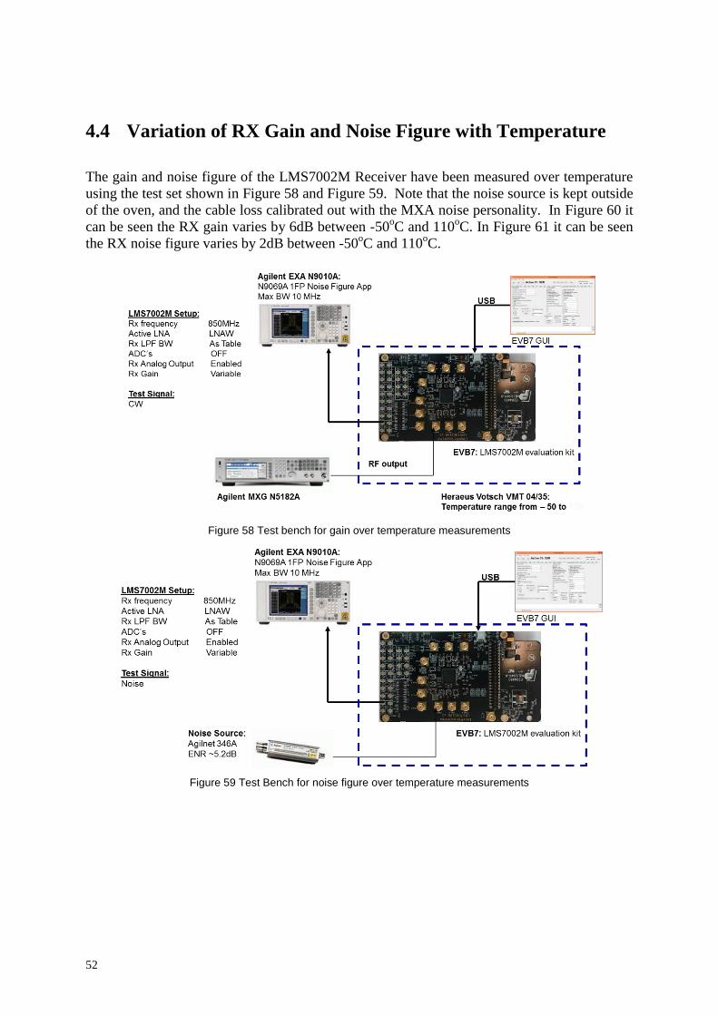
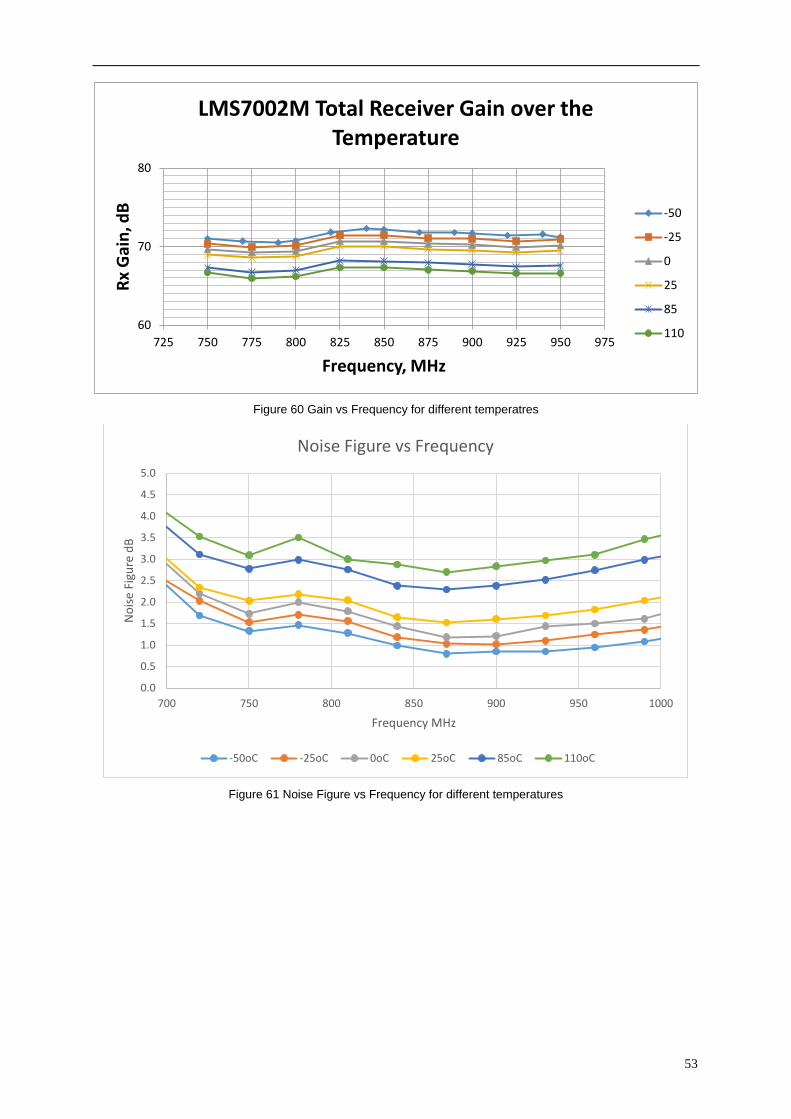
4.4 Variation of RX Gain and Noise Figure with Temperature
The gain and noise figure of the LMS7002M Receiver have been measured over temperature
using the test set shown in Figure 58 and Figure 59. Note that the noise source is kept outside
of the oven, and the cable loss calibrated out with the MXA noise personality. In Figure 60 it
can be seen the RX gain varies by 6dB between -50oC and 110
oC. In Figure 61 it can be seen
the RX noise figure varies by 2dB between -50oC and 110
oC.
Figure 58 Test bench for gain over temperature measurements
Figure 59 Test Bench for noise figure over temperature measurements
53
Figure 60 Gain vs Frequency for different temperatres
Figure 61 Noise Figure vs Frequency for different temperatures
60
70
80
725 750 775 800 825 850 875 900 925 950 975
Rx
Gai
n, d
B
Frequency, MHz
LMS7002M Total Receiver Gain over the Temperature
-50
-25
0
25
85
110
0.0
0.5
1.0
1.5
2.0
2.5
3.0
3.5
4.0
4.5
5.0
700 750 800 850 900 950 1000
No
ise
Figu
re d
B
Frequency MHz
Noise Figure vs Frequency
-50oC -25oC 0oC 25oC 85oC 110oC
54
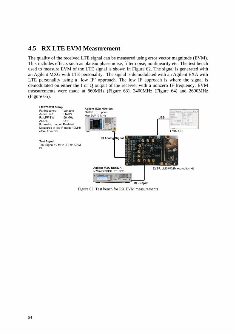
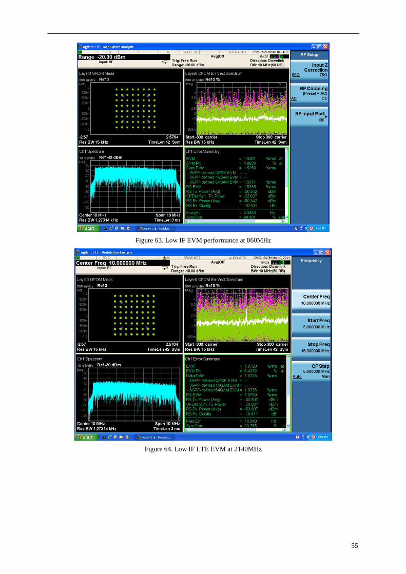
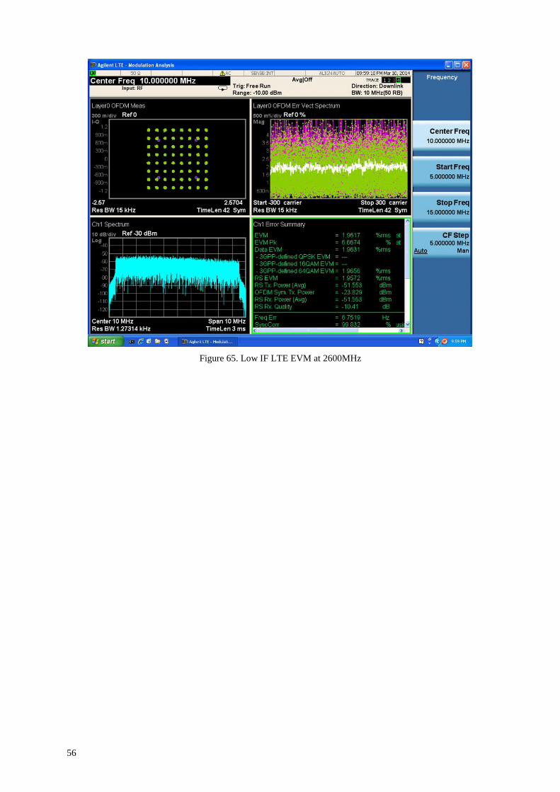
4.5 RX LTE EVM Measurement
The quality of the received LTE signal can be measured using error vector magnitude (EVM).
This includes effects such as plateau phase noise, filter noise, nonlinearity etc. The test bench
used to measure EVM of the LTE signal is shown in Figure 62. The signal is generated with
an Agilent MXG with LTE personality. The signal is demodulated with an Agilent EXA with
LTE personality using a ‘low IF’ approach. The low IF approach is where the signal is
demodulated on either the I or Q output of the receiver with a nonzero IF frequency. EVM
measurements were made at 860MHz (Figure 63), 2400MHz (Figure 64) and 2600MHz
(Figure 65).
Figure 62. Test bench for RX EVM measurements
55
Figure 63. Low IF EVM performance at 860MHz
Figure 64. Low IF LTE EVM at 2140MHz
56
Figure 65. Low IF LTE EVM at 2600MHz
57
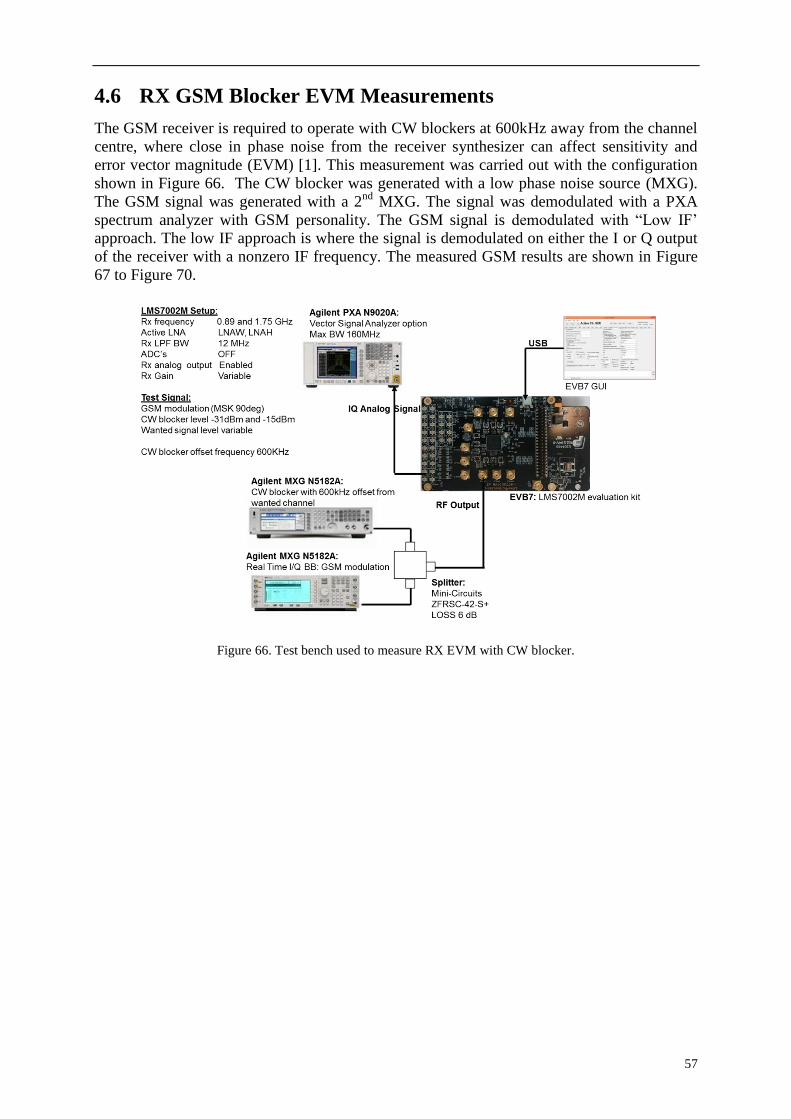
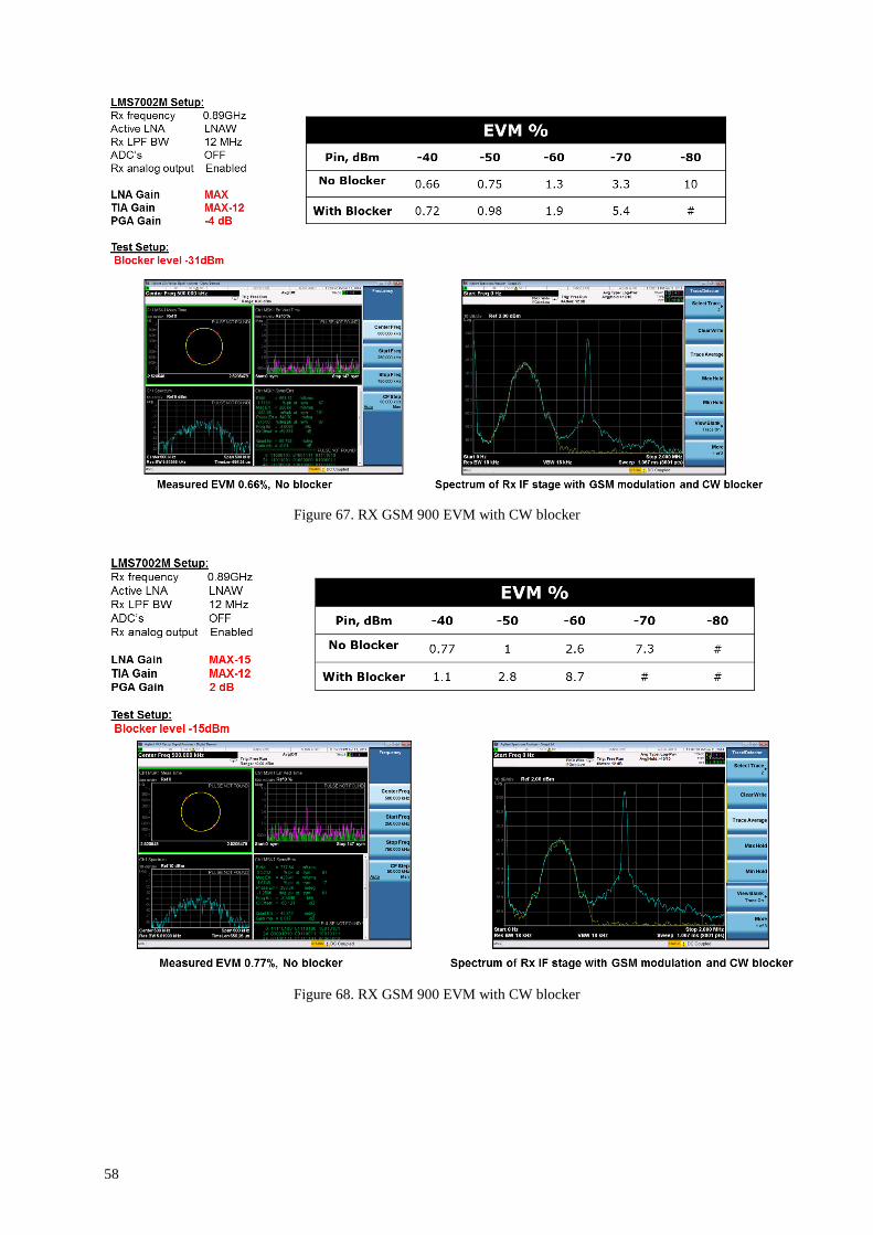
4.6 RX GSM Blocker EVM Measurements
The GSM receiver is required to operate with CW blockers at 600kHz away from the channel
centre, where close in phase noise from the receiver synthesizer can affect sensitivity and
error vector magnitude (EVM) [1]. This measurement was carried out with the configuration
shown in Figure 66. The CW blocker was generated with a low phase noise source (MXG).
The GSM signal was generated with a 2nd
MXG. The signal was demodulated with a PXA
spectrum analyzer with GSM personality. The GSM signal is demodulated with “Low IF’
approach. The low IF approach is where the signal is demodulated on either the I or Q output
of the receiver with a nonzero IF frequency. The measured GSM results are shown in Figure
67 to Figure 70.
Figure 66. Test bench used to measure RX EVM with CW blocker.
58
Figure 67. RX GSM 900 EVM with CW blocker
Figure 68. RX GSM 900 EVM with CW blocker
59
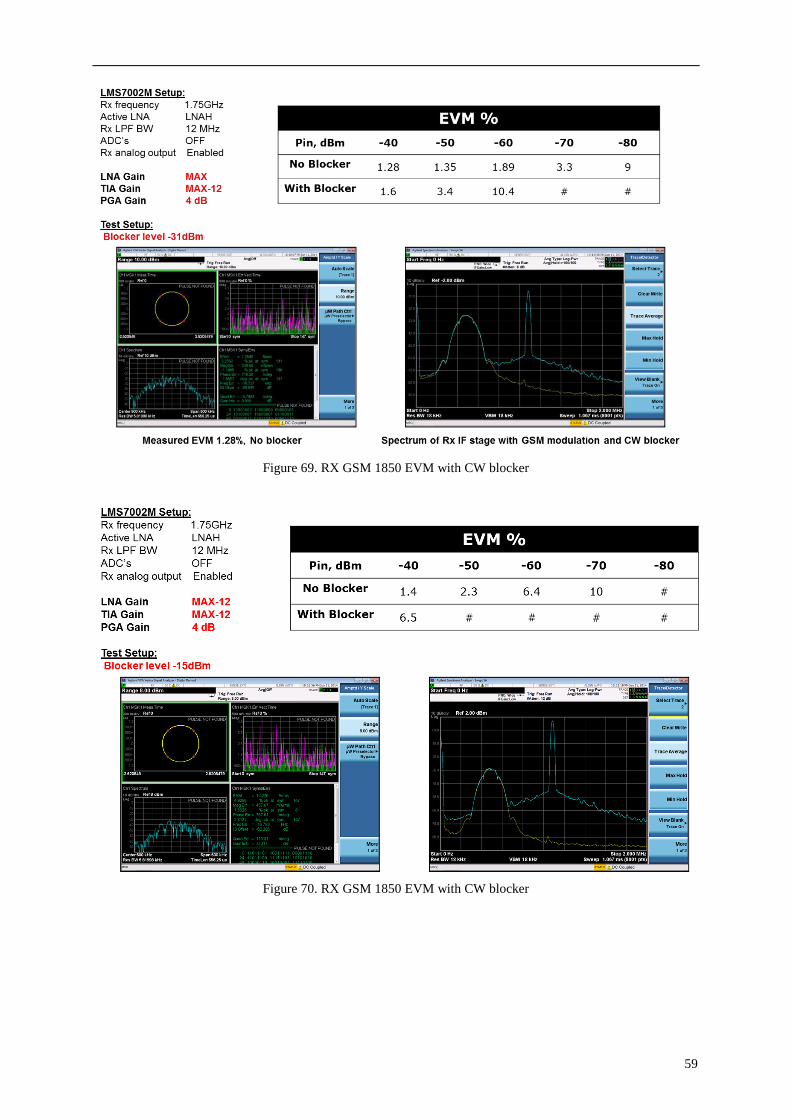
Figure 69. RX GSM 1850 EVM with CW blocker
Figure 70. RX GSM 1850 EVM with CW blocker
60
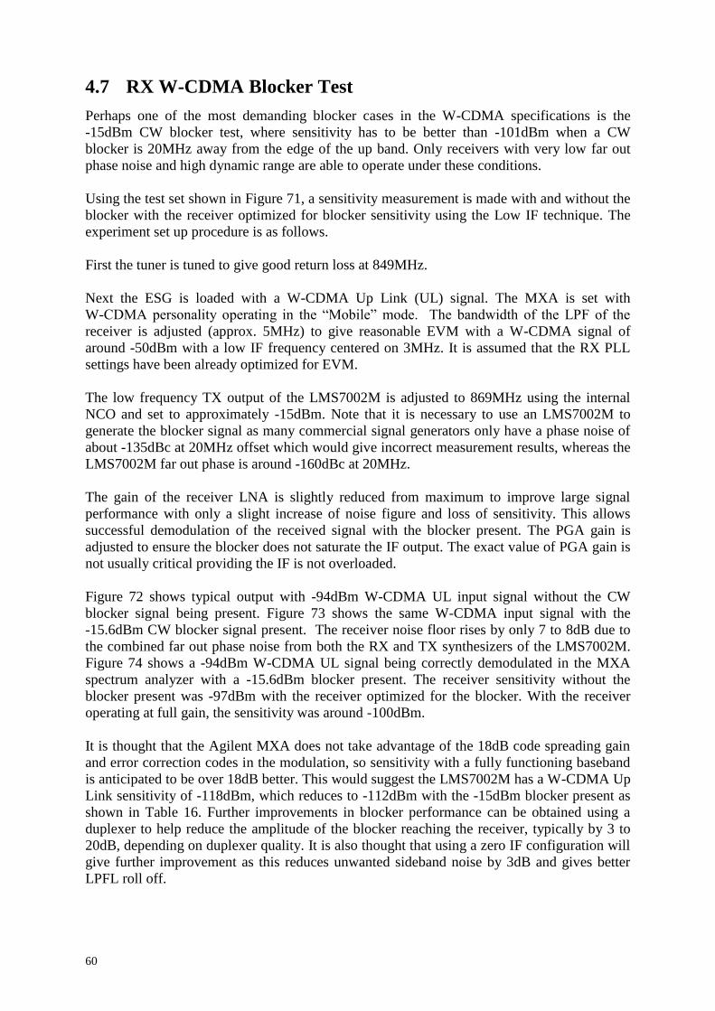
4.7 RX W-CDMA Blocker Test
Perhaps one of the most demanding blocker cases in the W-CDMA specifications is the
-15dBm CW blocker test, where sensitivity has to be better than -101dBm when a CW
blocker is 20MHz away from the edge of the up band. Only receivers with very low far out
phase noise and high dynamic range are able to operate under these conditions.
Using the test set shown in Figure 71, a sensitivity measurement is made with and without the
blocker with the receiver optimized for blocker sensitivity using the Low IF technique. The
experiment set up procedure is as follows.
First the tuner is tuned to give good return loss at 849MHz.
Next the ESG is loaded with a W-CDMA Up Link (UL) signal. The MXA is set with
W-CDMA personality operating in the “Mobile” mode. The bandwidth of the LPF of the
receiver is adjusted (approx. 5MHz) to give reasonable EVM with a W-CDMA signal of
around -50dBm with a low IF frequency centered on 3MHz. It is assumed that the RX PLL
settings have been already optimized for EVM.
The low frequency TX output of the LMS7002M is adjusted to 869MHz using the internal
NCO and set to approximately -15dBm. Note that it is necessary to use an LMS7002M to
generate the blocker signal as many commercial signal generators only have a phase noise of
about -135dBc at 20MHz offset which would give incorrect measurement results, whereas the
LMS7002M far out phase is around -160dBc at 20MHz.
The gain of the receiver LNA is slightly reduced from maximum to improve large signal
performance with only a slight increase of noise figure and loss of sensitivity. This allows
successful demodulation of the received signal with the blocker present. The PGA gain is
adjusted to ensure the blocker does not saturate the IF output. The exact value of PGA gain is
not usually critical providing the IF is not overloaded.
Figure 72 shows typical output with -94dBm W-CDMA UL input signal without the CW
blocker signal being present. Figure 73 shows the same W-CDMA input signal with the
-15.6dBm CW blocker signal present. The receiver noise floor rises by only 7 to 8dB due to
the combined far out phase noise from both the RX and TX synthesizers of the LMS7002M.
Figure 74 shows a -94dBm W-CDMA UL signal being correctly demodulated in the MXA
spectrum analyzer with a -15.6dBm blocker present. The receiver sensitivity without the
blocker present was -97dBm with the receiver optimized for the blocker. With the receiver
operating at full gain, the sensitivity was around -100dBm.
It is thought that the Agilent MXA does not take advantage of the 18dB code spreading gain
and error correction codes in the modulation, so sensitivity with a fully functioning baseband
is anticipated to be over 18dB better. This would suggest the LMS7002M has a W-CDMA Up
Link sensitivity of -118dBm, which reduces to -112dBm with the -15dBm blocker present as
shown in Table 16. Further improvements in blocker performance can be obtained using a
duplexer to help reduce the amplitude of the blocker reaching the receiver, typically by 3 to
20dB, depending on duplexer quality. It is also thought that using a zero IF configuration will
give further improvement as this reduces unwanted sideband noise by 3dB and gives better
LPFL roll off.
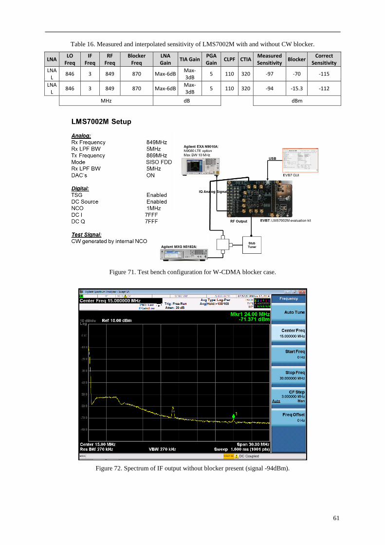
61
Table 16. Measured and interpolated sensitivity of LMS7002M with and without CW blocker.
LNA LO
Freq IF
Freq RF
Freq Blocker
Freq LNA Gain
TIA Gain PGA Gain
CLPF CTIA Measured Sensitivity
Blocker Correct
Sensitivity
LNAL
846 3 849 870 Max-6dB Max-3dB
5 110 320 -97 -70 -115
LNAL
846 3 849 870 Max-6dB Max-3dB
5 110 320 -94 -15.3 -112
MHz dB
dBm
Figure 71. Test bench configuration for W-CDMA blocker case.
Figure 72. Spectrum of IF output without blocker present (signal -94dBm).
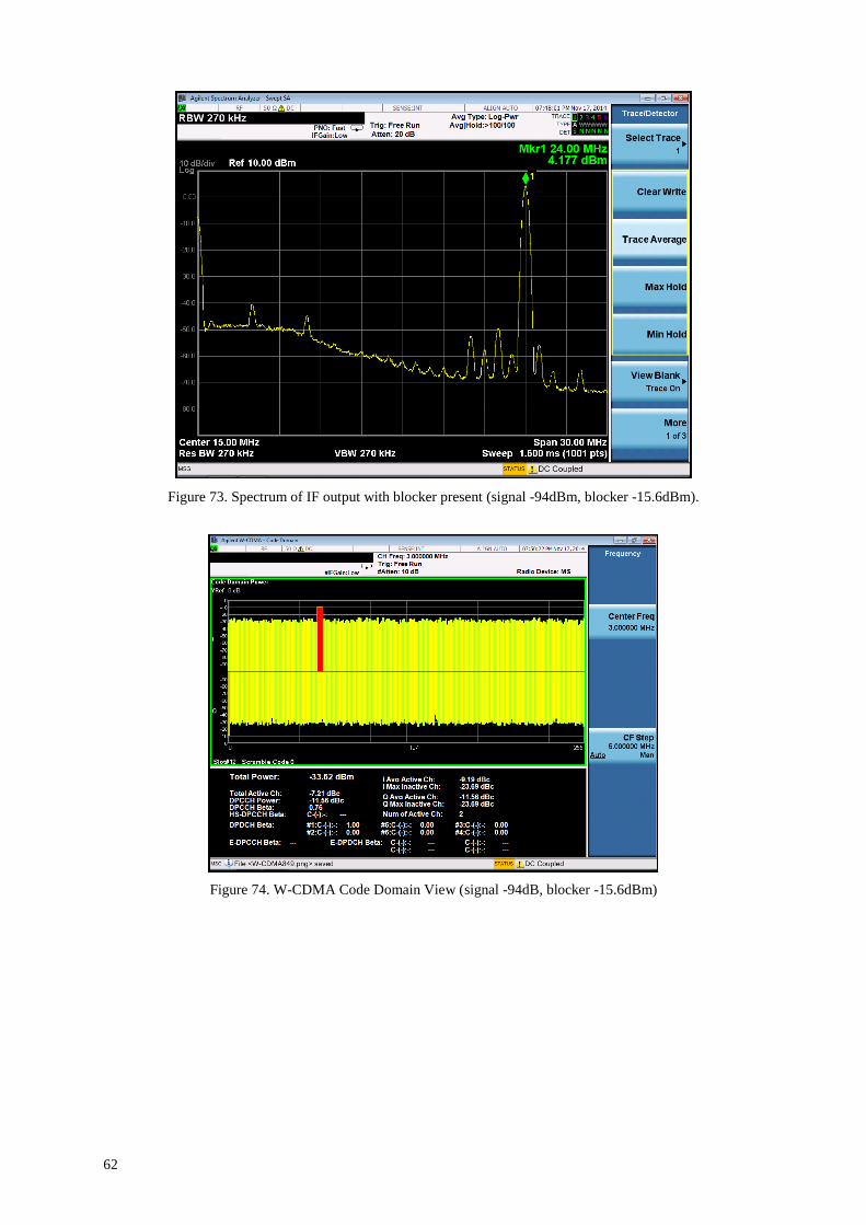
62
Figure 73. Spectrum of IF output with blocker present (signal -94dBm, blocker -15.6dBm).
Figure 74. W-CDMA Code Domain View (signal -94dB, blocker -15.6dBm)
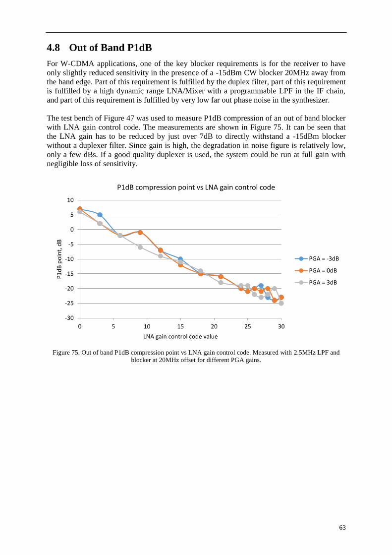
63
4.8 Out of Band P1dB
For W-CDMA applications, one of the key blocker requirements is for the receiver to have
only slightly reduced sensitivity in the presence of a -15dBm CW blocker 20MHz away from
the band edge. Part of this requirement is fulfilled by the duplex filter, part of this requirement
is fulfilled by a high dynamic range LNA/Mixer with a programmable LPF in the IF chain,
and part of this requirement is fulfilled by very low far out phase noise in the synthesizer.
The test bench of Figure 47 was used to measure P1dB compression of an out of band blocker
with LNA gain control code. The measurements are shown in Figure 75. It can be seen that
the LNA gain has to be reduced by just over 7dB to directly withstand a -15dBm blocker
without a duplexer filter. Since gain is high, the degradation in noise figure is relatively low,
only a few dBs. If a good quality duplexer is used, the system could be run at full gain with
negligible loss of sensitivity.
Figure 75. Out of band P1dB compression point vs LNA gain control code. Measured with 2.5MHz LPF and
blocker at 20MHz offset for different PGA gains.
-30
-25
-20
-15
-10
-5
0
5
10
0 5 10 15 20 25 30
P1
dB
po
int,
dB
LNA gain control code value
P1dB compression point vs LNA gain control code
PGA = -3dB
PGA = 0dB
PGA = 3dB
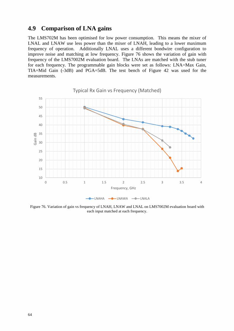
64
4.9 Comparison of LNA gains
The LMS702M has been optimised for low power consumption. This means the mixer of
LNAL and LNAW use less power than the mixer of LNAH, leading to a lower maximum
frequency of operation. Additionally LNAL uses a different bondwire configuration to
improve noise and matching at low frequency. Figure 76 shows the variation of gain with
frequency of the LMS7002M evaluation board. The LNAs are matched with the stub tuner
for each frequency. The programmable gain blocks were set as follows: LNA=Max Gain,
TIA=Mid Gain (-3dB) and PGA=5dB. The test bench of Figure 42 was used for the
measurements.
Figure 76. Variation of gain vs frequency of LNAH, LNAW and LNAL on LMS7002M evaluation board with
each input matched at each frequency.
10
15
20
25
30
35
40
45
50
55
0 0.5 1 1.5 2 2.5 3 3.5 4
Gai
n d
B
Frequency, GHz
Typical Rx Gain vs Frequency (Matched)
LNAHA LNAWA LNALA
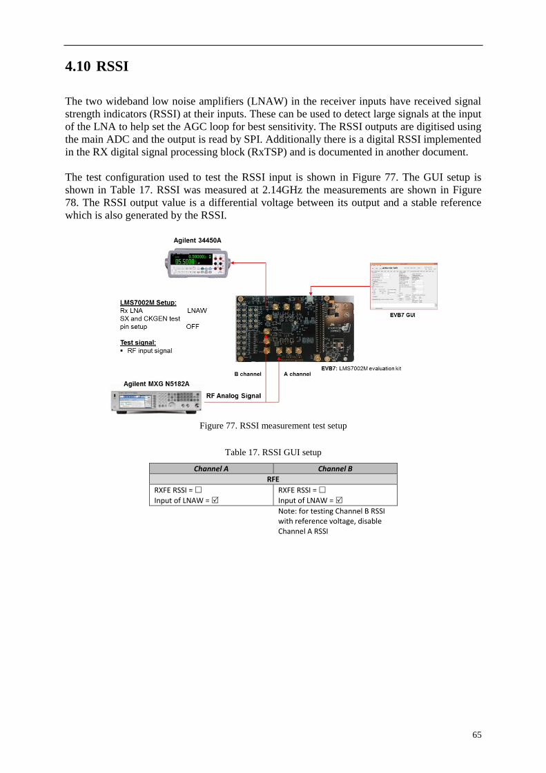
65
4.10 RSSI
The two wideband low noise amplifiers (LNAW) in the receiver inputs have received signal
strength indicators (RSSI) at their inputs. These can be used to detect large signals at the input
of the LNA to help set the AGC loop for best sensitivity. The RSSI outputs are digitised using
the main ADC and the output is read by SPI. Additionally there is a digital RSSI implemented
in the RX digital signal processing block (RxTSP) and is documented in another document.
The test configuration used to test the RSSI input is shown in Figure 77. The GUI setup is
shown in Table 17. RSSI was measured at 2.14GHz the measurements are shown in Figure
78. The RSSI output value is a differential voltage between its output and a stable reference
which is also generated by the RSSI.
Figure 77. RSSI measurement test setup
Table 17. RSSI GUI setup
Channel A Channel B
RFE
RXFE RSSI = RXFE RSSI =
Input of LNAW = Input of LNAW =
Note: for testing Channel B RSSI with reference voltage, disable Channel A RSSI
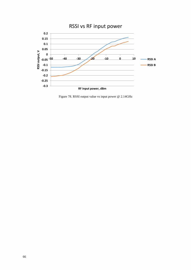
66
Figure 78. RSSI output value vs input power @ 2.14GHz
-0.3
-0.25
-0.2
-0.15
-0.1
-0.05
0
0.05
0.1
0.15
0.2
-50 -40 -30 -20 -10 0 10
RSS
I o
utp
ut,
V
RF input power, dBm
RSSI vs RF input power
RSSI A
RSSI B
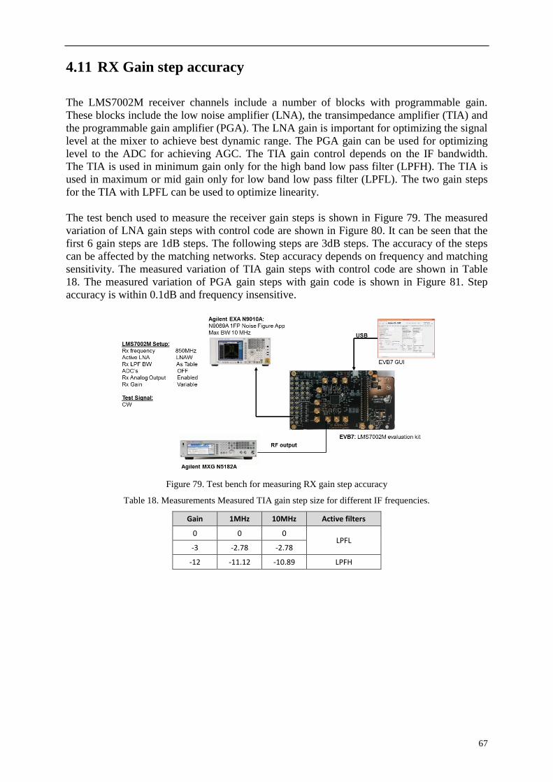
67
4.11 RX Gain step accuracy
The LMS7002M receiver channels include a number of blocks with programmable gain.
These blocks include the low noise amplifier (LNA), the transimpedance amplifier (TIA) and
the programmable gain amplifier (PGA). The LNA gain is important for optimizing the signal
level at the mixer to achieve best dynamic range. The PGA gain can be used for optimizing
level to the ADC for achieving AGC. The TIA gain control depends on the IF bandwidth.
The TIA is used in minimum gain only for the high band low pass filter (LPFH). The TIA is
used in maximum or mid gain only for low band low pass filter (LPFL). The two gain steps
for the TIA with LPFL can be used to optimize linearity.
The test bench used to measure the receiver gain steps is shown in Figure 79. The measured
variation of LNA gain steps with control code are shown in Figure 80. It can be seen that the
first 6 gain steps are 1dB steps. The following steps are 3dB steps. The accuracy of the steps
can be affected by the matching networks. Step accuracy depends on frequency and matching
sensitivity. The measured variation of TIA gain steps with control code are shown in Table
18. The measured variation of PGA gain steps with gain code is shown in Figure 81. Step
accuracy is within 0.1dB and frequency insensitive.
Figure 79. Test bench for measuring RX gain step accuracy
Table 18. Measurements Measured TIA gain step size for different IF frequencies.
Gain 1MHz 10MHz Active filters
0 0 0 LPFL
-3 -2.78 -2.78
-12 -11.12 -10.89 LPFH
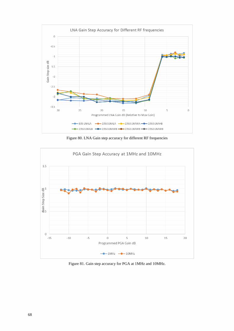
68
Figure 80. LNA Gain step accuracy for different RF frequencies
Figure 81. Gain step accuracy for PGA at 1MHz and 10MHz.
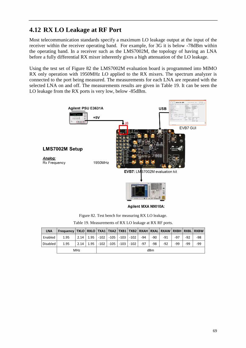
69
4.12 RX LO Leakage at RF Port
Most telecommunication standards specify a maximum LO leakage output at the input of the
receiver within the receiver operating band. For example, for 3G it is below -78dBm within
the operating band. In a receiver such as the LMS7002M, the topology of having an LNA
before a fully differential RX mixer inherently gives a high attenuation of the LO leakage.
Using the test set of Figure 82 the LMS7002M evaluation board is programmed into MIMO
RX only operation with 1950MHz LO applied to the RX mixers. The spectrum analyzer is
connected to the port being measured. The measurements for each LNA are repeated with the
selected LNA on and off. The measurements results are given in Table 19. It can be seen the
LO leakage from the RX ports is very low, below -85dBm.
Figure 82. Test bench for measuring RX LO leakage.
Table 19. Measurements of RX LO leakage at RX RF ports.
LNA Frequency TXLO RXLO TXA1 TXA2 TXB1 TXB2 RXAH RXAL RXAW RXBH RXBL RXBW
Enabled 1.95 2.14 1.95 -102 -105 -103 -102 -94 -90 -91 -97 -92 -98
Disabled 1.95 2.14 1.95 -102 -105 -103 -102 -97 -98 -92 -99 -99 -99
MHz dBm
70
5 Loop Back Measurements
The LMS7002M provides 3 types of loop back for the purpose of calibration and testing.
These are RF loopback, baseband analog loopback and digital loopback. Section 5.1 describes
the performance and set up of the baseband loopback. Section 5.2 describes the performance
and set up of the RF loopback. Digital loopback will be discussed in a separate document.
5.1 Baseband Loopback
The baseband loopback is primarily intended to be used for calibration. This includes LO
leakage, image rejection and the frequency response of the TX low band and high band low
pass filters. The filters require calibration as ‘on chip’ resistors and capacitors are vulnerable
to significant variation of absolute value (up to about +/-20%).
The baseband loopback can also be used to implement various self test functions. It provides
a flexible means to route low frequency baseband signals without using the RF outputs or RF
loopback. It allows various combinations of low pass filters to be either selected or bypassed.
The most useful combinations of the available routing are given in Table 20.
Baseband loopback requires significant set up. The TSP is configured to generated test
signals from 1MHz to 50MHz by means of the DAC, CLKGEN PLL and the TSP NCO. The
CLKGEN PLL is programmed for 240MHz clocking to allow tone generation up to 60MHz.
The DAC is generally set with a current of 625uA. For calibrating the TX low pass filters, it
is best to route the baseband loopback directly to the RX programmable gain amplifier.
The baseband test bench is shown in Figure 83. Typical frequency responses of the baseband
loopback are shown in Figure 84. In this case, the TXLPFL was programmed for 10MHz,
with the TX real pole set to 2MHz. The RXLPFL was programmed for 5MHz. The TXLPFH
and RXLPFH were programmed for a cut off frequency greater than 70MHz. The PGA is set
with 0dB gain. The IAMP is set with a gain of 32.
Although the baseband loopback allows access to the RX low pass filters, they cannot be fully
calibrated in baseband loopback as the TIA includes a pole necessary to produce the full 3rd
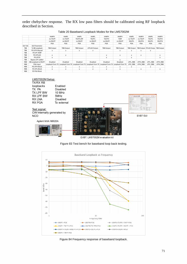
71
order chebychev response. The RX low pass filters should be calibrated using RF loopback
described in Section.
Table 20 Baseband Loopback Modes for the LMS7002M
Figure 83 Test bench for baseband loop back testing.
Figure 84 Frequency response of baseband loopback.
IAMPH IAMPL IAMPL IAMPL IAMPH IAMPH IAMPL IAMPH IAMPL IAMPH
no TXLPF no TXLPF TXLPFL+RP TXLPFL TXLPFH TXRP no TXLPF no TXLPF TXLPFL TXLPFH
no RXLPF no RXLPF no RXLPF no RXLPF no RXLPF no RXLPF RXLPFL RXLPFH RXLPFL RXLPFH
PGA PGA PGA PGA PGA PGA PGA PGA PGA PGA
GUI Tab GUI Parameter
TBB Tx BB Loopback TBB Output TBB Output TBB Output LPFLAD Output TBB Output TBB Output TBB Output TBB OutputLPFLAD OutputTBB Output
TBB PD LPFH Biquad y y y y y y y y
TBB PD LPF IAMP
TBB PD LPFLAD y y y y y y y
TBB PD LPFS5 y y y y
TBB Bypass LPF Ladder y
RBB BB Loopback to RXLPF Disabled Disabled Disabled Disabled Disabled Disabled LPFL_RBB LPFH_RBB LPFL_RBB LPFH_RBB
RBB PGA input Loopback from TX Loopback from TX Loopback from TX Loopback from TX Loopback from TX Loopback from TX LPFL_RBB LPFH_RBB LPFL_RBB LPFH_RBB
RBB PD LPFH Block y y y y y y y y
RBB PD LPFL Block y y y y y y y y
RBB PD PGA Block

72
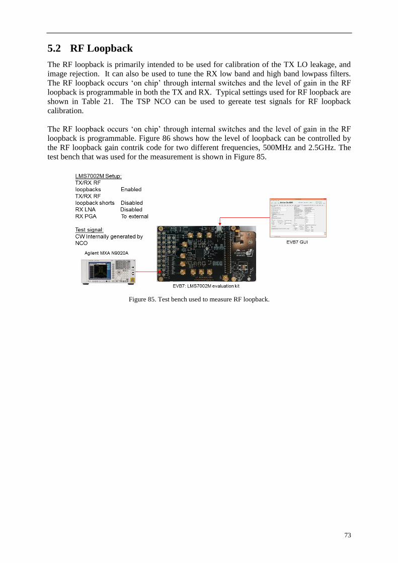
73
5.2 RF Loopback
The RF loopback is primarily intended to be used for calibration of the TX LO leakage, and
image rejection. It can also be used to tune the RX low band and high band lowpass filters.
The RF loopback occurs ‘on chip’ through internal switches and the level of gain in the RF
loopback is programmable in both the TX and RX. Typical settings used for RF loopback are
shown in Table 21. The TSP NCO can be used to gereate test signals for RF loopback
calibration.
The RF loopback occurs ‘on chip’ through internal switches and the level of gain in the RF
loopback is programmable. Figure 86 shows how the level of loopback can be controlled by
the RF loopback gain contrik code for two different frequencies, 500MHz and 2.5GHz. The
test bench that was used for the measurement is shown in Figure 85.
Figure 85. Test bench used to measure RF loopback.
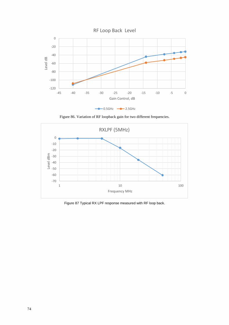
74
Figure 86. Variation of RF loopback gain for two different frequencies.
Figure 87 Typical RX LPF response measured with RF loop back.
-120
-100
-80
-60
-40
-20
0
-45 -40 -35 -30 -25 -20 -15 -10 -5 0
Leve
l dB
Gain Control, dB
RF Loop Back Level
0.5GHz 2.5GHz
-70
-60
-50
-40
-30
-20
-10
0
1 10 100
Leve
l dB
m
Frequency MHz
RXLPF (5MHz)
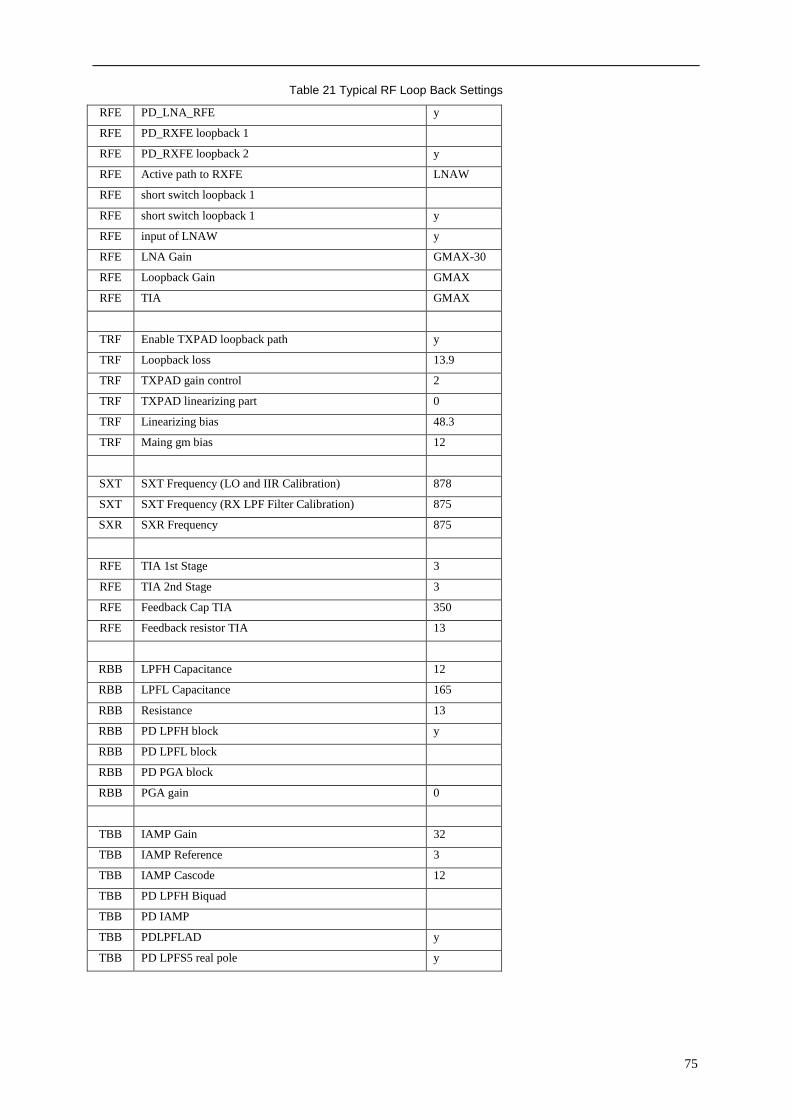
75
Table 21 Typical RF Loop Back Settings
RFE PD_LNA_RFE y
RFE PD_RXFE loopback 1
RFE PD_RXFE loopback 2 y
RFE Active path to RXFE LNAW
RFE short switch loopback 1
RFE short switch loopback 1 y
RFE input of LNAW y
RFE LNA Gain GMAX-30
RFE Loopback Gain GMAX
RFE TIA GMAX
TRF Enable TXPAD loopback path y
TRF Loopback loss 13.9
TRF TXPAD gain control 2
TRF TXPAD linearizing part 0
TRF Linearizing bias 48.3
TRF Maing gm bias 12
SXT SXT Frequency (LO and IIR Calibration) 878
SXT SXT Frequency (RX LPF Filter Calibration) 875
SXR SXR Frequency 875
RFE TIA 1st Stage 3
RFE TIA 2nd Stage 3
RFE Feedback Cap TIA 350
RFE Feedback resistor TIA 13
RBB LPFH Capacitance 12
RBB LPFL Capacitance 165
RBB Resistance 13
RBB PD LPFH block y
RBB PD LPFL block
RBB PD PGA block
RBB PGA gain 0
TBB IAMP Gain 32
TBB IAMP Reference 3
TBB IAMP Cascode 12
TBB PD LPFH Biquad
TBB PD IAMP
TBB PDLPFLAD y
TBB PD LPFS5 real pole y
76
6 Miscellaneous Measurements
This chapter presents a number of measurements. Section 6.1 describes DC power dissipation
for different modes of operation. Section 6.2 describes the variation of the internal Low Drop
Out Regulators (LDO) voltage with control code. Section 6.3 describes the measurement of
the noise of the internal LDOs.
6.1 Power dissipation
The LMS7002M uses low voltage CMOS technology which leads to low power operation.
The LMS7002M is highly reconfigurable, capable of operating in a number of modes
including RX only, TX only, Frequency Division Duplexing (FDD), Time Division Duplex
(TDD) which use both RX and TX simultaneously. Additionally there are single in single out
(SISO) or multiple in or multiple out (MIMO) modes. The MIMO mode uses two RX or TX
channels simultaneously.
Power dissipation is measured with the test bench shown in Figure 88.
Table 22 shows the power dissipation when the LMS7002M operates in SISO mode, as an
RX or TX only. Generally the RX alone in SISO mode uses 160-260mW depending on
routing and operating frequency. Generally the TX alone in SISO mode uses 240-380mW at
maximum output power, depending on routing and operating frequency. Power can be
reduced by reducing output power in TPAD. Note, although the B channel is intended for
MIMO operation, it is possible to operate the transceiver with the B channel in SISO
operation, e.g. to provide matching for additional bands.
Table 23 shows the power dissipation when the LMS7002M operates in SISO mode, in either
FDD or TDD mode. Generally FDD in SISO mode uses between 404-650mW at maximum
output power, depending on routing and operating frequency. Power can be reduced by
reducing output power in TPAD. Generally TDD in SISO mode uses between 325-650mW at
maximum output power, depending on routing and operating frequency. Power can be
77
reduced by reducing output power in TPAD. The TDD power dissipation is lower than FDD
power dissipation as only one PLL is active.
78
Table 24 shows the power dissipation when the LMS7002M operates in MIMO mode, as an
RX or TX only. Generally the RX alone in SISO mode uses 220-330mW depending on
routing and operating frequency. Generally the TX alone in SISO mode uses 380-550mW at
maximum output power, depending on routing and operating frequency. Power can be
reduced by reducing output power in TPAD.
Table 25 shows the power dissipation when the LMS7002M operates in MIMO mode, in
either FDD or TDD mode. Generally FDD in SISO mode uses between 595-870mW at
maximum output power, depending on routing and operating frequency. Power can be
reduced by reducing output power in TPAD. Generally TDD in SISO mode uses between
510-865mW at maximum output power, depending on routing and operating frequency.
Power can be reduced by reducing output power in TPAD. The TDD power dissipation is
lower than FDD power dissipation as only one PLL is active.
Note that these tests used only the analog part of the transceiver. The digital power dissipation
will be presented in a separate document and depends on both clock frequency and
functionality.
Figure 88. Test bench used to measure power dissipation
Table 22. Comparison of power dissipation of LMS7002M operating either in TX or RX SISO mode for
different frequencies.
Mode RXA RXB TXA TXB RX/TX PLL PDISS mW
Power down OFF OFF OFF OFF OFF 0
SISO-RX LNAH OFF OFF OFF 30 161.98
SISO-RX LNAH OFF OFF OFF 835 183.54
SISO-RX LNAH OFF OFF OFF 1950 166.18
SISO-RX LNAH OFF OFF OFF 3800 214.76
SISO-RX LNAL OFF OFF OFF 835 185.08
SISO-RX LNAL OFF OFF OFF 1950 172.34
SISO-RX LNAW OFF OFF OFF 1950 182.84
SISO-RX OFF LNAH OFF OFF 1950 187.74
SISO-RX OFF LNAH OFF OFF 3800 255.22
SISO-RX OFF LNAL OFF OFF 835 191.94
SISO-RX OFF LNAL OFF OFF 1950 193.76
79
Mode RXA RXB TXA TXB RX/TX PLL PDISS mW
SISO-RX OFF LNAW OFF OFF 1950 202.3
SISO-TX OFF OFF TX1 OFF 30 241.92
SISO-TX OFF OFF TX1 OFF 875 273.28
SISO-TX OFF OFF TX1 OFF 2140 271.04
SISO-TX OFF OFF TX1 OFF 3800 335.86
SISO-TX OFF OFF TX2 OFF 2140 275.52
SISO-TX OFF OFF OFF TX1 2140 318.22
SISO-TX OFF OFF OFF TX1 3800 388.92
SISO-TX OFF OFF OFF TX2 2140 312.2
Table 23. Comparison of power dissipation of LMS7002M operating either in SISO FDD and TDD mode for
different frequencies.
Mode RXA RXB TXA TXB RX/TX PLL PDISS mW
SISO-FDD LNAH OFF TX1 OFF 1950/2140 514.36
SISO-FDD LNAH OFF TX1 OFF 3450/3550 647.64
SISO-FDD LNAL OFF TX2 OFF 30/40 412.3
SISO-FDD LNAL OFF TX2 OFF 835/875 480.48
SISO-FDD LNAL OFF TX2 OFF 1950/2140 504.7
SISO-FDD LNAW OFF TX2 OFF 1950/2140 506.24
SISO-FDD OFF LNAH OFF TX1 1950/2140 504.98
SISO-FDD OFF LNAH OFF TX1 3450/3550 627.2
SISO-FDD OFF LNAL OFF TX2 30/40 404.6
SISO-FDD OFF LNAL OFF TX2 835/875 472.22
SISO-FDD OFF LNAL OFF TX2 1950/2140 505.12
SISO-FDD OFF LNAW OFF TX2 1950/2140 505.26
SISO-TDD LNAH OFF TX1 OFF 2140 499.8
SISO-TDD LNAH OFF TX1 OFF 3800 649.6
SISO-TDD LNAL OFF TX2 OFF 30 325.78
SISO-TDD LNAL OFF TX2 OFF 2140 507.64
SISO-TDD OFF LNAH OFF TX1 2140 485.94
SISO-TDD OFF LNAH OFF TX1 3800 621.18
SISO-TDD OFF LNAL OFF TX2 30 309.26
SISO-TDD OFF LNAL OFF TX2 2140 486.5
SISO-TDD OFF LNAW OFF TX2 2140 495.32
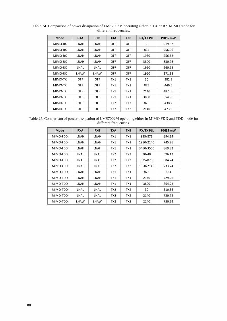
80
Table 24. Comparison of power dissipation of LMS7002M operating either in TX or RX MIMO mode for
different frequencies.
Mode RXA RXB TXA TXB RX/TX PLL PDISS mW
MIMO-RX LNAH LNAH OFF OFF 30 219.52
MIMO-RX LNAH LNAH OFF OFF 835 256.06
MIMO-RX LNAH LNAH OFF OFF 1950 256.62
MIMO-RX LNAH LNAH OFF OFF 3800 330.96
MIMO-RX LNAL LNAL OFF OFF 1950 260.68
MIMO-RX LNAW LNAW OFF OFF 1950 271.18
MIMO-TX OFF OFF TX1 TX1 30 382.9
MIMO-TX OFF OFF TX1 TX1 875 446.6
MIMO-TX OFF OFF TX1 TX1 2140 487.06
MIMO-TX OFF OFF TX1 TX1 3800 554.96
MIMO-TX OFF OFF TX2 TX2 875 438.2
MIMO-TX OFF OFF TX2 TX2 2140 473.9
Table 25. Comparison of power dissipation of LMS7002M operating either in MIMO FDD and TDD mode for
different frequencies.
Mode RXA RXB TXA TXB RX/TX PLL PDISS mW
MIMO-FDD LNAH LNAH TX1 TX1 835/875 694.54
MIMO-FDD LNAH LNAH TX1 TX1 1950/2140 745.36
MIMO-FDD LNAH LNAH TX1 TX1 3450/3550 869.82
MIMO-FDD LNAL LNAL TX2 TX2 30/40 596.12
MIMO-FDD LNAL LNAL TX2 TX2 835/875 684.74
MIMO-FDD LNAL LNAL TX2 TX2 1950/2140 733.74
MIMO-TDD LNAH LNAH TX1 TX1 875 623
MIMO-TDD LNAH LNAH TX1 TX1 2140 729.26
MIMO-TDD LNAH LNAH TX1 TX1 3800 864.22
MIMO-TDD LNAL LNAL TX2 TX2 30 510.86
MIMO-TDD LNAL LNAL TX2 TX2 2140 720.72
MIMO-TDD LNAW LNAW TX2 TX2 2140 730.24
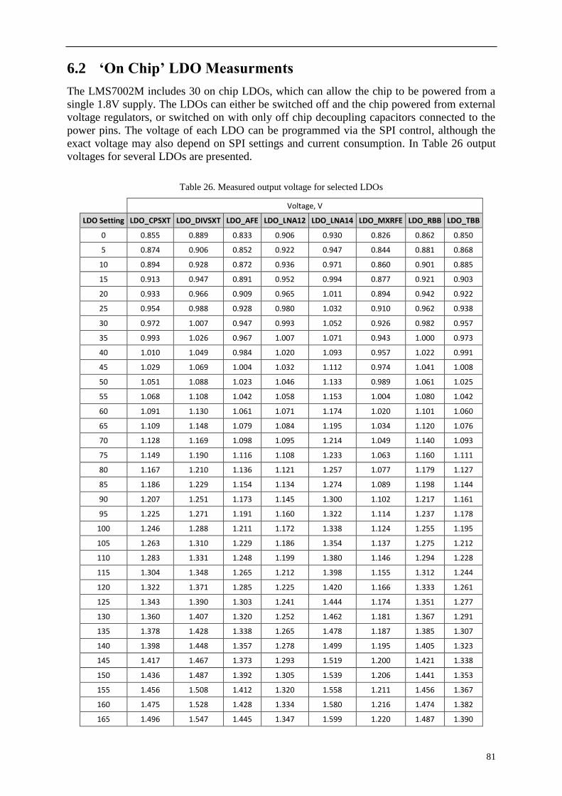
81
6.2 ‘On Chip’ LDO Measurments
The LMS7002M includes 30 on chip LDOs, which can allow the chip to be powered from a
single 1.8V supply. The LDOs can either be switched off and the chip powered from external
voltage regulators, or switched on with only off chip decoupling capacitors connected to the
power pins. The voltage of each LDO can be programmed via the SPI control, although the
exact voltage may also depend on SPI settings and current consumption. In Table 26 output
voltages for several LDOs are presented.
Table 26. Measured output voltage for selected LDOs
Voltage, V
LDO Setting LDO_CPSXT LDO_DIVSXT LDO_AFE LDO_LNA12 LDO_LNA14 LDO_MXRFE LDO_RBB LDO_TBB
0 0.855 0.889 0.833 0.906 0.930 0.826 0.862 0.850
5 0.874 0.906 0.852 0.922 0.947 0.844 0.881 0.868
10 0.894 0.928 0.872 0.936 0.971 0.860 0.901 0.885
15 0.913 0.947 0.891 0.952 0.994 0.877 0.921 0.903
20 0.933 0.966 0.909 0.965 1.011 0.894 0.942 0.922
25 0.954 0.988 0.928 0.980 1.032 0.910 0.962 0.938
30 0.972 1.007 0.947 0.993 1.052 0.926 0.982 0.957
35 0.993 1.026 0.967 1.007 1.071 0.943 1.000 0.973
40 1.010 1.049 0.984 1.020 1.093 0.957 1.022 0.991
45 1.029 1.069 1.004 1.032 1.112 0.974 1.041 1.008
50 1.051 1.088 1.023 1.046 1.133 0.989 1.061 1.025
55 1.068 1.108 1.042 1.058 1.153 1.004 1.080 1.042
60 1.091 1.130 1.061 1.071 1.174 1.020 1.101 1.060
65 1.109 1.148 1.079 1.084 1.195 1.034 1.120 1.076
70 1.128 1.169 1.098 1.095 1.214 1.049 1.140 1.093
75 1.149 1.190 1.116 1.108 1.233 1.063 1.160 1.111
80 1.167 1.210 1.136 1.121 1.257 1.077 1.179 1.127
85 1.186 1.229 1.154 1.134 1.274 1.089 1.198 1.144
90 1.207 1.251 1.173 1.145 1.300 1.102 1.217 1.161
95 1.225 1.271 1.191 1.160 1.322 1.114 1.237 1.178
100 1.246 1.288 1.211 1.172 1.338 1.124 1.255 1.195
105 1.263 1.310 1.229 1.186 1.354 1.137 1.275 1.212
110 1.283 1.331 1.248 1.199 1.380 1.146 1.294 1.228
115 1.304 1.348 1.265 1.212 1.398 1.155 1.312 1.244
120 1.322 1.371 1.285 1.225 1.420 1.166 1.333 1.261
125 1.343 1.390 1.303 1.241 1.444 1.174 1.351 1.277
130 1.360 1.407 1.320 1.252 1.462 1.181 1.367 1.291
135 1.378 1.428 1.338 1.265 1.478 1.187 1.385 1.307
140 1.398 1.448 1.357 1.278 1.499 1.195 1.405 1.323
145 1.417 1.467 1.373 1.293 1.519 1.200 1.421 1.338
150 1.436 1.487 1.392 1.305 1.539 1.206 1.441 1.353
155 1.456 1.508 1.412 1.320 1.558 1.211 1.456 1.367
160 1.475 1.528 1.428 1.334 1.580 1.216 1.474 1.382
165 1.496 1.547 1.445 1.347 1.599 1.220 1.487 1.390
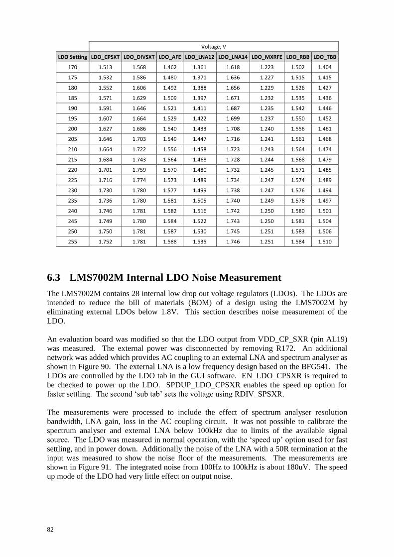
82
Voltage, V
LDO Setting LDO_CPSXT LDO_DIVSXT LDO_AFE LDO_LNA12 LDO_LNA14 LDO_MXRFE LDO_RBB LDO_TBB
170 1.513 1.568 1.462 1.361 1.618 1.223 1.502 1.404
175 1.532 1.586 1.480 1.371 1.636 1.227 1.515 1.415
180 1.552 1.606 1.492 1.388 1.656 1.229 1.526 1.427
185 1.571 1.629 1.509 1.397 1.671 1.232 1.535 1.436
190 1.591 1.646 1.521 1.411 1.687 1.235 1.542 1.446
195 1.607 1.664 1.529 1.422 1.699 1.237 1.550 1.452
200 1.627 1.686 1.540 1.433 1.708 1.240 1.556 1.461
205 1.646 1.703 1.549 1.447 1.716 1.241 1.561 1.468
210 1.664 1.722 1.556 1.458 1.723 1.243 1.564 1.474
215 1.684 1.743 1.564 1.468 1.728 1.244 1.568 1.479
220 1.701 1.759 1.570 1.480 1.732 1.245 1.571 1.485
225 1.716 1.774 1.573 1.489 1.734 1.247 1.574 1.489
230 1.730 1.780 1.577 1.499 1.738 1.247 1.576 1.494
235 1.736 1.780 1.581 1.505 1.740 1.249 1.578 1.497
240 1.746 1.781 1.582 1.516 1.742 1.250 1.580 1.501
245 1.749 1.780 1.584 1.522 1.743 1.250 1.581 1.504
250 1.750 1.781 1.587 1.530 1.745 1.251 1.583 1.506
255 1.752 1.781 1.588 1.535 1.746 1.251 1.584 1.510
6.3 LMS7002M Internal LDO Noise Measurement
The LMS7002M contains 28 internal low drop out voltage regulators (LDOs). The LDOs are
intended to reduce the bill of materials (BOM) of a design using the LMS7002M by
eliminating external LDOs below 1.8V. This section describes noise measurement of the
LDO.
An evaluation board was modified so that the LDO output from VDD_CP_SXR (pin AL19)
was measured. The external power was disconnected by removing R172. An additional
network was added which provides AC coupling to an external LNA and spectrum analyser as
shown in Figure 90. The external LNA is a low frequency design based on the BFG541. The
LDOs are controlled by the LDO tab in the GUI software. EN_LDO_CPSXR is required to
be checked to power up the LDO. SPDUP_LDO_CPSXR enables the speed up option for
faster settling. The second ‘sub tab’ sets the voltage using RDIV_SPSXR.
The measurements were processed to include the effect of spectrum analyser resolution
bandwidth, LNA gain, loss in the AC coupling circuit. It was not possible to calibrate the
spectrum analyser and external LNA below 100kHz due to limits of the available signal
source. The LDO was measured in normal operation, with the ‘speed up’ option used for fast
settling, and in power down. Additionally the noise of the LNA with a 50R termination at the
input was measured to show the noise floor of the measurements. The measurements are
shown in Figure 91. The integrated noise from 100Hz to 100kHz is about 180uV. The speed
up mode of the LDO had very little effect on output noise.
83
Figure 89 Test configuration used to measure noise.
LDO output
pin (AL19)
1uF
100Ohm
LNA
100Ohm
10uF
100Ohm Agilent spectrum analyzer
EXA N9010A
Figure 90 AC coupling circuit used for LDO noise measurement.
Figure 91 Measured LDO noise of the LDO with LNA for different LDO modes.
0.1
1
10
100
1000
10000
0.1 1 10 100 1000 10000
No
ise
nV
/RtH
z
Frequency kHz
Internal LDO Noise vs Frequency
LDO+LNA LDO_Spdup+LNA LDO_PD+LNA 50R+LNA


![Universal Radio Development Platform User Guide€¦ · Cyclone IV device family, refer to Cyclone IV Device Handbook [link] LMS7002M transceiver resources [link] LMS6002D transceiver](https://img.pdfslide.net/doc/110x75/5f4cd5dda18a3763564e8a92/universal-radio-development-platform-user-guide-cyclone-iv-device-family-refer.jpg)