Embed Size (px)
Citation preview
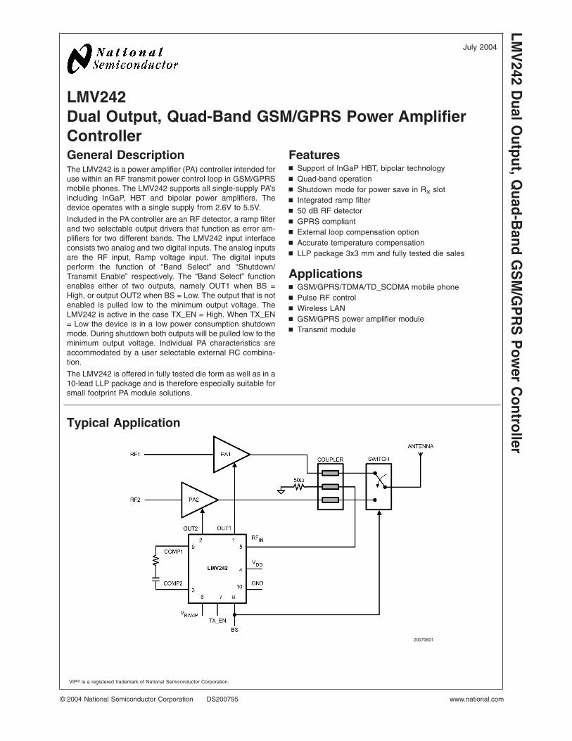
LMV242Dual Output, Quad-Band GSM/GPRS Power AmplifierControllerGeneral DescriptionThe LMV242 is a power amplifier (PA) controller intended foruse within an RF transmit power control loop in GSM/GPRSmobile phones. The LMV242 supports all single-supply PA’sincluding InGaP, HBT and bipolar power amplifiers. Thedevice operates with a single supply from 2.6V to 5.5V.
Included in the PA controller are an RF detector, a ramp filterand two selectable output drivers that function as error am-plifiers for two different bands. The LMV242 input interfaceconsists two analog and two digital inputs. The analog inputsare the RF input, Ramp voltage input. The digital inputsperform the function of “Band Select” and “Shutdown/Transmit Enable” respectively. The “Band Select” functionenables either of two outputs, namely OUT1 when BS =High, or output OUT2 when BS = Low. The output that is notenabled is pulled low to the minimum output voltage. TheLMV242 is active in the case TX_EN = High. When TX_EN= Low the device is in a low power consumption shutdownmode. During shutdown both outputs will be pulled low to theminimum output voltage. Individual PA characteristics areaccommodated by a user selectable external RC combina-tion.
The LMV242 is offered in fully tested die form as well as in a10-lead LLP package and is therefore especially suitable forsmall footprint PA module solutions.
Featuresn Support of InGaP HBT, bipolar technologyn Quad-band operationn Shutdown mode for power save in RX slotn Integrated ramp filtern 50 dB RF detectorn GPRS compliantn External loop compensation optionn Accurate temperature compensationn LLP package 3x3 mm and fully tested die sales
Applicationsn GSM/GPRS/TDMA/TD_SCDMA mobile phonen Pulse RF controln Wireless LANn GSM/GPRS power amplifier modulen Transmit module
Typical Application
20079501
VIP® is a registered trademark of National Semiconductor Corporation.
July 2004LM
V242
DualO
utput,Quad-B
andG
SM
/GP
RS
Pow
erC
ontroller
© 2004 National Semiconductor Corporation DS200795 www.national.com
Absolute Maximum Ratings (Note 1)
If Military/Aerospace specified devices are required,please contact the National Semiconductor Sales Office/Distributors for availability and specifications.
Supply Voltage
VDD - GND 6.5V Max
ESD Tolerance (Note 2)
Human Body Model 2 kV
Machine Model 200V
Storage Temperature Range −65˚C to 150˚C
Junction Temperature (Note 6) 150˚C Max
Mounting Temperature
Infrared or convection (20 sec) 235˚C
Operating Ratings (Note 1)
Supply Voltage 2.6V to 5.5V
Operating TemperatureRange −40˚C to +85˚C
VRAMP Voltage Range 0V to 2V
RF Frequency Range 450 MHz to 2 GHz
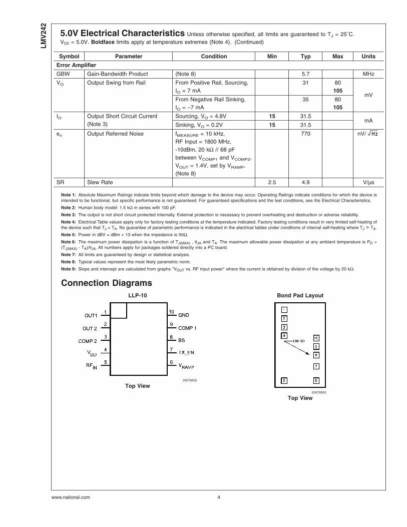
2.6V Electrical Characteristics Unless otherwise specified, all limits are guaranteed to TJ = 25˚C.VDD = 2.6V. Boldface limits apply at temperature extremes (Note 4).
Symbol Parameter Condition Min Typ Max Units
IDD Supply Current VOUT = (VDD - GND)/2 6.9 912
mA
In Shutdown (TX_EN = 0V)VOUT = (VDD - GND)/2
0.2 30 µA
VHIGH Logic Level to Enable Power (Note 7) 1.8 V
VLOW Logic Level to Disable Power (Note 7) 0.8 V
TON Turn-on-Time from Shutdown 3.6 6 µs
IEN, IBS Current into TX_EN and BS Pin 0.03 5 µA
RAMP Amplifier
VRD VRAMP Deadband 155 206 265 mV
1/RRAMP Transconductance (Note 8) 70 96 120 µA/V
IOUT RAMP Ramp Amplifier Output Current VRAMP = 2V 100 162 µA
RF Input
PIN RF Input Power Range (Note 5) 20 kΩ // 68 pF betweenVCOMP1 and VCOMP2
−500
dBm
−63−13
dBV
Logarithmic Slope (Note 9) @ 900 MHz, 20 kΩ // 68 pFbetween VCOMP1 and VCOMP2
−1.74
µA/dB
@ 1800 MHz, 20 kΩ // 68 pFbetween VCOMP1 and VCOMP2
−1.62
@ 1900 MHz, 20 kΩ // 68 pFbetween VCOMP1 and VCOMP2
−1.60
@ 2000 MHz, 20 kΩ // 68 pFbetween VCOMP1 and VCOMP2
−1.59
Logarithmic Intercept (Note 9) @ 900 MHz, 20 kΩ // 68 pFbetween VCOMP1 and VCOMP2
–50.4
dBm
@ 1800 MHz, 20 kΩ // 68 ifbetween VCOMP1 and VCOMP2
–52.3
@ 1900 MHz, 20 kΩ // 68 pFbetween VCOMP1 and VCOMP2
–51.9
@ 2000 MHz, 20 kΩ // 68 pFbetween VCOMP1 and VCOMP2
–52.3
RIN DC Resistance (Note 8) 55.7 ΩError Amplifier
GBW Gain-Bandwidth Product (Note 8) 5.1 MHz
LMV
242
www.national.com 2
2.6V Electrical Characteristics Unless otherwise specified, all limits are guaranteed to TJ = 25˚C.VDD = 2.6V. Boldface limits apply at temperature extremes (Note 4). (Continued)
Symbol Parameter Condition Min Typ Max Units
VO Output Swing from Rail From Positive Rail, Sourcing,IO = 7 mA
47 90115
mVFrom Negative Rail Sinking,IO = −7 mA
52 90115
IO Output Short Circuit Current(Note 3)
Sourcing, VO = 2.4V 10 29.5mA
Sinking, VO. = 0.2V 10 27.1
en Output Referred Noise fMEASURE = 10 KHz,RF Input = 1800 MHz, -10dBm, 20 kΩ // 68 pF betweenVCOMP1 and VCOMP2, VOUT
=1.4V, set by VRAMP, (Note 8)
700 nV/
SR Slew Rate 2.1 4.4 V/µs
5.0V Electrical Characteristics Unless otherwise specified, all limits are guaranteed to TJ = 25˚C.VDD = 5.0V. Boldface limits apply at temperature extremes (Note 4).
Symbol Parameter Condition Min Typ Max Units
IDD Supply Current VOUT = (VDD - GND)/2 7.8 1215
mA
In Shutdown (TX_EN = 0V)VOUT = (VDD - GND)/2
0.4 30 µA
VHIGH Logic Level to Enable Power (Note 7) 1.8 V
VLOW Logic Level to Disable Power (Note 7) 0.8 V
TON Turn-on-Time from Shutdown 1.5 6 µs
IEN, IBS Current into TX_EN and BS Pin 0.03 5 µA
RAMP Amplifier
VRD VRAMP Deadband 155 206 265 mV
1/RRAMP Transconductance (Note 8) 70 96 120 µA/V
IOUT RAMP Ramp Amplifier Output Current VRAMP = 2V 100 168 µA
RF Input
PIN RF Input Power Range(Note 5)
20 kΩ // 68 pF betweenVCOMP1 and VCOMP2
−500
dBm
−63−13
dBV
Logarithmic Slope(Note 9)
@ 900 MHz, 20 kΩ // 68 pFbetween VCOMP1 and VCOMP2
−1.79
µA/dB
@ 1800 MHz, 20 kΩ // 68 pFbetween VCOMP1 and VCOMP2
–1.69
@ 1900 MHz, 20 kΩ // 68 pFbetween VCOMP1 and VCOMP2
−1.67
@ 2000 MHz, 20 kΩ // 68 pFbetween VCOMP1 and VCOMP2
–1.65
Logarithmic Intercept(Note 9)
@ 900 MHz, 20 kΩ // 68 pFbetween VCOMP1 and VCOMP2
–50.2
dBm
@ 1800 MHz, 20 kΩ // 68 pFbetween VCOMP1 and VCOMP2
–52.5
@ 1900 MHz, 20 kΩ // 68 pFbetween VCOMP1 and VCOMP2
–52.5
@ 2000 MHz, 20 kΩ // 68 pFbetween VCOMP1 and VCOMP2
–52.9
RIN DC Resistance (Note 8) 55.7 Ω
LMV
242
www.national.com3
5.0V Electrical Characteristics Unless otherwise specified, all limits are guaranteed to TJ = 25˚C.VDD = 5.0V. Boldface limits apply at temperature extremes (Note 4). (Continued)
Symbol Parameter Condition Min Typ Max Units
Error Amplifier
GBW Gain-Bandwidth Product (Note 8) 5.7 MHz
VO Output Swing from Rail From Positive Rail, Sourcing,IO = 7 mA
31 80105
mVFrom Negative Rail Sinking,IO = −7 mA
35 80105
IO Output Short Circuit Current(Note 3)
Sourcing, VO = 4.8V 15 31.5mA
Sinking, VO = 0.2V 15 31.5
en Output Referred Noise fMEASURE = 10 kHz,RF Input = 1800 MHz,-10dBm, 20 kΩ // 68 pFbetween VCOMP1 and VCOMP2,VOUT = 1.4V, set by VRAMP,(Note 8)
770 nV/
SR Slew Rate 2.5 4.9 V/µs
Note 1: Absolute Maximum Ratings indicate limits beyond which damage to the device may occur. Operating Ratings indicate conditions for which the device isintended to be functional, but specific performance is not guaranteed. For guaranteed specifications and the test conditions, see the Electrical Characteristics.
Note 2: Human body model: 1.5 kΩ in series with 100 pF.
Note 3: The output is not short circuit protected internally. External protection is necessary to prevent overheating and destruction or adverse reliability.
Note 4: Electrical Table values apply only for factory testing conditions at the temperature indicated. Factory testing conditions result in very limited self-heating ofthe device such that TJ = TA. No guarantee of parametric performance is indicated in the electrical tables under conditions of internal self-heating where TJ > TA.
Note 5: Power in dBV = dBm + 13 when the impedance is 50Ω.
Note 6: The maximum power dissipation is a function of TJ(MAX) , θJA and TA. The maximum allowable power dissipation at any ambient temperature is PD =(TJ(MAX) - TA)/θJA. All numbers apply for packages soldered directly into a PC board.
Note 7: All limits are guaranteed by design or statistical analysis.
Note 8: Typical values represent the most likely parametric norm.
Note 9: Slope and intercept are calculated from graphs "VOUT vs. RF input power" where the current is obtained by division of the voltage by 20 kΩ.
Connection DiagramsLLP-10 Bond Pad Layout
20079502
Top View20079503
Top View
LMV
242
www.national.com 4
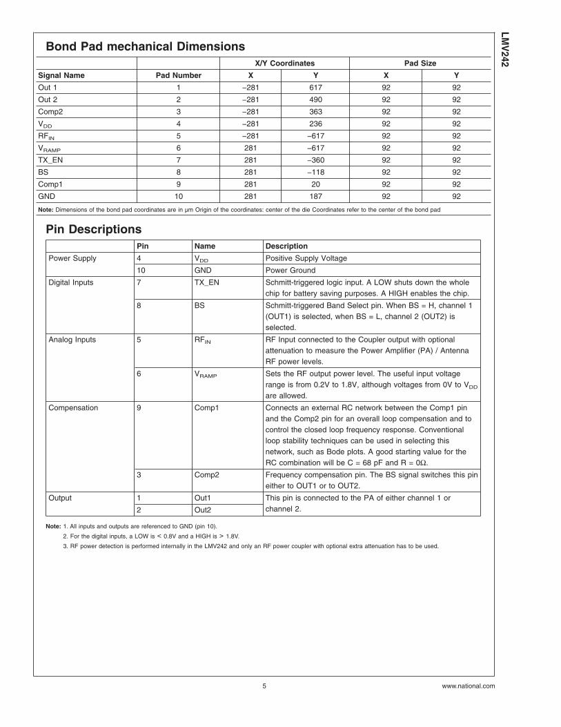
Bond Pad mechanical DimensionsX/Y Coordinates Pad Size
Signal Name Pad Number X Y X Y
Out 1 1 −281 617 92 92
Out 2 2 −281 490 92 92
Comp2 3 −281 363 92 92
VDD 4 −281 236 92 92
RFIN 5 −281 −617 92 92
VRAMP 6 281 −617 92 92
TX_EN 7 281 −360 92 92
BS 8 281 −118 92 92
Comp1 9 281 20 92 92
GND 10 281 187 92 92
Note: Dimensions of the bond pad coordinates are in µm Origin of the coordinates: center of the die Coordinates refer to the center of the bond pad
Pin DescriptionsPin Name Description
Power Supply 4 VDD Positive Supply Voltage
10 GND Power Ground
Digital Inputs 7 TX_EN Schmitt-triggered logic input. A LOW shuts down the wholechip for battery saving purposes. A HIGH enables the chip.
8 BS Schmitt-triggered Band Select pin. When BS = H, channel 1(OUT1) is selected, when BS = L, channel 2 (OUT2) isselected.
Analog Inputs 5 RFIN RF Input connected to the Coupler output with optionalattenuation to measure the Power Amplifier (PA) / AntennaRF power levels.
6 VRAMP Sets the RF output power level. The useful input voltagerange is from 0.2V to 1.8V, although voltages from 0V to VDD
are allowed.
Compensation 9 Comp1 Connects an external RC network between the Comp1 pinand the Comp2 pin for an overall loop compensation and tocontrol the closed loop frequency response. Conventionalloop stability techniques can be used in selecting thisnetwork, such as Bode plots. A good starting value for theRC combination will be C = 68 pF and R = 0Ω.
3 Comp2 Frequency compensation pin. The BS signal switches this pineither to OUT1 or to OUT2.
Output 1 Out1 This pin is connected to the PA of either channel 1 orchannel 2.2 Out2
Note: 1. All inputs and outputs are referenced to GND (pin 10).
2. For the digital inputs, a LOW is < 0.8V and a HIGH is > 1.8V.
3. RF power detection is performed internally in the LMV242 and only an RF power coupler with optional extra attenuation has to be used.
LMV
242
www.national.com5
Ordering Information
Package Part Number Package Marking Transport Media NSC Drawing
10-Pin LLPLMV242LD
242LD1k Units Tape and Reel
LDA10ALMV242LDX 4.5k Units tape and Reel
Tested and WaferForm
LMV242MDANo Mark
300 Units Waffle Pack DA0620035
LMV242MWA 25 Wafer/Vial W008
Block Diagram
20079504
LMV
242
www.national.com 6
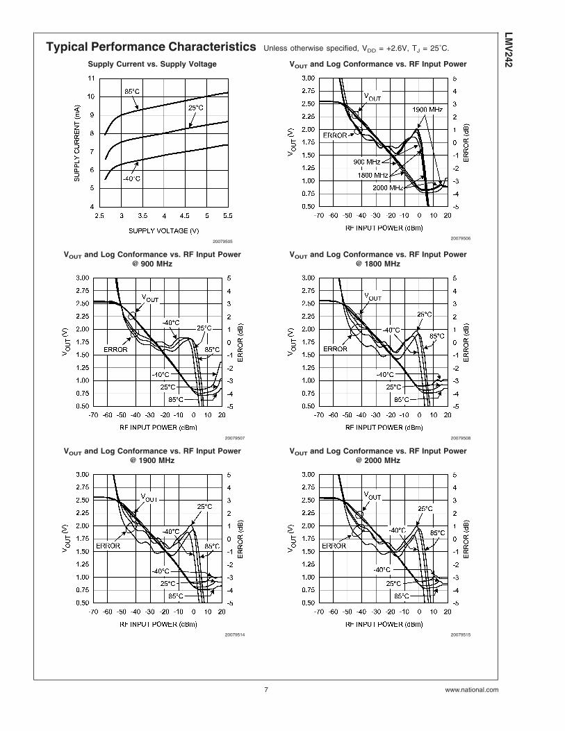
Typical Performance Characteristics Unless otherwise specified, VDD = +2.6V, TJ = 25˚C.
Supply Current vs. Supply Voltage VOUT and Log Conformance vs. RF Input Power
2007950520079506
VOUT and Log Conformance vs. RF Input Power@ 900 MHz
VOUT and Log Conformance vs. RF Input Power@ 1800 MHz
20079507 20079508
VOUT and Log Conformance vs. RF Input Power@ 1900 MHz
VOUT and Log Conformance vs. RF Input Power@ 2000 MHz
20079514 20079515
LMV
242
www.national.com7
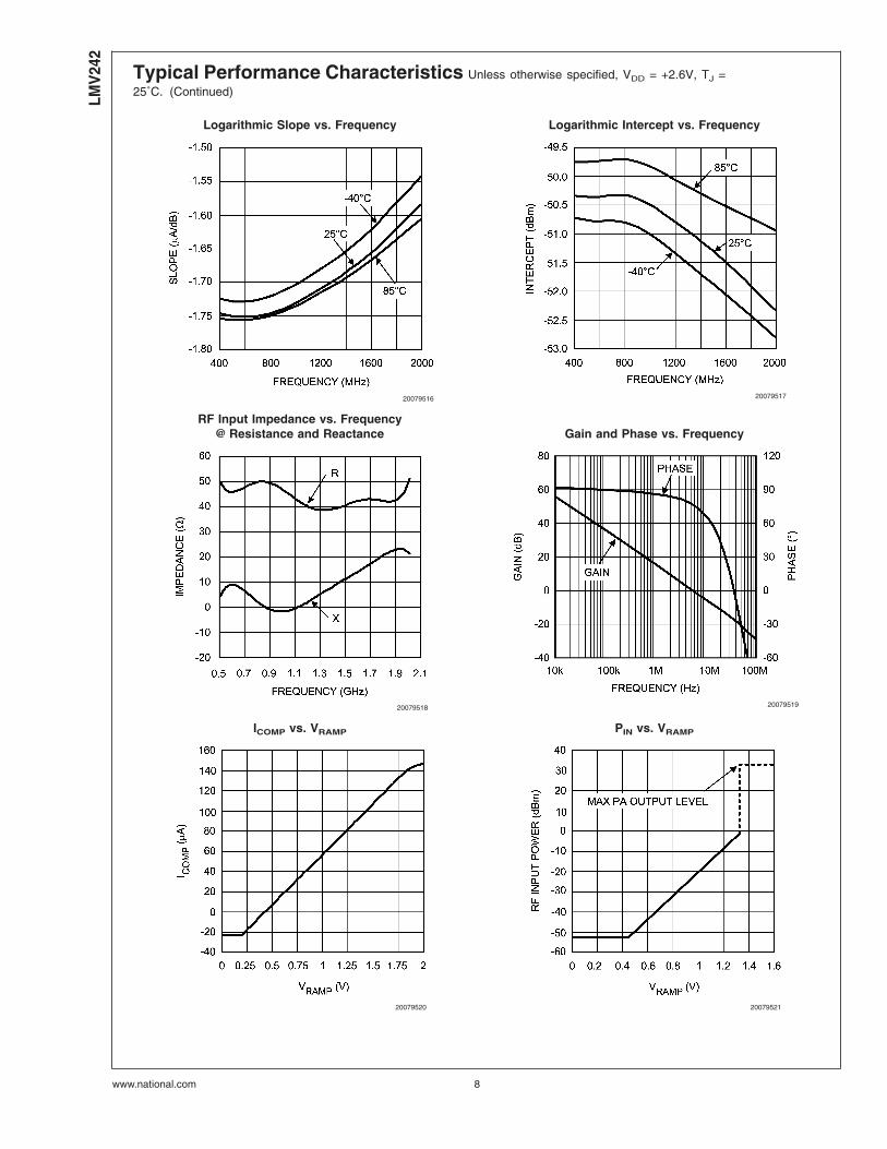
Typical Performance Characteristics Unless otherwise specified, VDD = +2.6V, TJ =25˚C. (Continued)
Logarithmic Slope vs. Frequency Logarithmic Intercept vs. Frequency
20079516 20079517
RF Input Impedance vs. Frequency@ Resistance and Reactance Gain and Phase vs. Frequency
20079518 20079519
ICOMP vs. VRAMP PIN vs. VRAMP
20079520 20079521
LMV
242
www.national.com 8
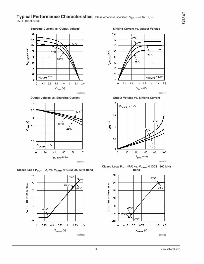
Typical Performance Characteristics Unless otherwise specified, VDD = +2.6V, TJ =25˚C. (Continued)
Sourcing Current vs. Output Voltage Sinking Current vs. Output Voltage
20079510 20079511
Output Voltage vs. Sourcing Current Output Voltage vs. Sinking Current
20079512 20079513
Closed Loop POUT (PA) vs. VRAMP @ GSM 900 MHz BandClosed Loop POUT (PA) vs. VRAMP @ DCS 1800 MHz
Band
20079522 20079523
LMV
242
www.national.com9
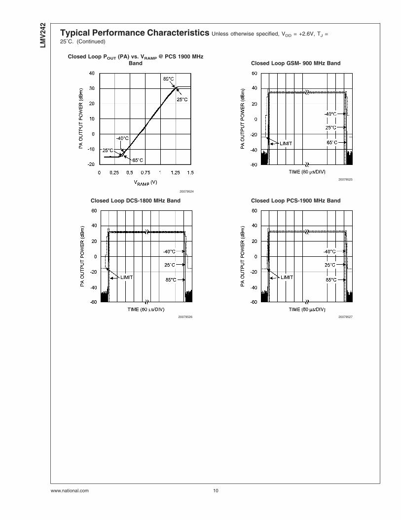
Typical Performance Characteristics Unless otherwise specified, VDD = +2.6V, TJ =25˚C. (Continued)
Closed Loop POUT (PA) vs. VRAMP @ PCS 1900 MHzBand Closed Loop GSM- 900 MHz Band
20079524
20079525
Closed Loop DCS-1800 MHz Band Closed Loop PCS-1900 MHz Band
20079526 20079527
LMV
242
www.national.com 10
Application Section
POWER CONTROL PRINCIPLES
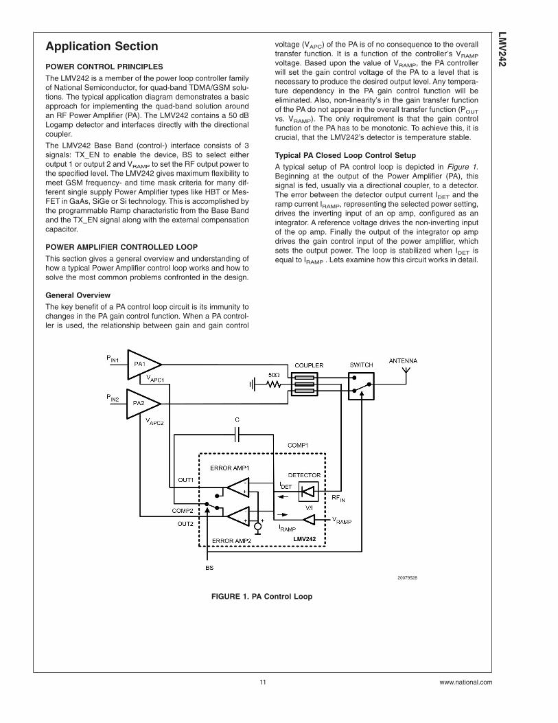
The LMV242 is a member of the power loop controller familyof National Semiconductor, for quad-band TDMA/GSM solu-tions. The typical application diagram demonstrates a basicapproach for implementing the quad-band solution aroundan RF Power Amplifier (PA). The LMV242 contains a 50 dBLogamp detector and interfaces directly with the directionalcoupler.
The LMV242 Base Band (control-) interface consists of 3signals: TX_EN to enable the device, BS to select eitheroutput 1 or output 2 and VRAMP to set the RF output power tothe specified level. The LMV242 gives maximum flexibility tomeet GSM frequency- and time mask criteria for many dif-ferent single supply Power Amplifier types like HBT or Mes-FET in GaAs, SiGe or Si technology. This is accomplished bythe programmable Ramp characteristic from the Base Bandand the TX_EN signal along with the external compensationcapacitor.
POWER AMPLIFIER CONTROLLED LOOP
This section gives a general overview and understanding ofhow a typical Power Amplifier control loop works and how tosolve the most common problems confronted in the design.
General Overview
The key benefit of a PA control loop circuit is its immunity tochanges in the PA gain control function. When a PA control-ler is used, the relationship between gain and gain control
voltage (VAPC) of the PA is of no consequence to the overalltransfer function. It is a function of the controller’s VRAMP
voltage. Based upon the value of VRAMP, the PA controllerwill set the gain control voltage of the PA to a level that isnecessary to produce the desired output level. Any tempera-ture dependency in the PA gain control function will beeliminated. Also, non-linearity’s in the gain transfer functionof the PA do not appear in the overall transfer function (POUT
vs. VRAMP). The only requirement is that the gain controlfunction of the PA has to be monotonic. To achieve this, it iscrucial, that the LMV242’s detector is temperature stable.
Typical PA Closed Loop Control Setup
A typical setup of PA control loop is depicted in Figure 1.Beginning at the output of the Power Amplifier (PA), thissignal is fed, usually via a directional coupler, to a detector.The error between the detector output current IDET and theramp current IRAMP, representing the selected power setting,drives the inverting input of an op amp, configured as anintegrator. A reference voltage drives the non-inverting inputof the op amp. Finally the output of the integrator op ampdrives the gain control input of the power amplifier, whichsets the output power. The loop is stabilized when IDET isequal to IRAMP . Lets examine how this circuit works in detail.
20079528
FIGURE 1. PA Control Loop
LMV
242
www.national.com11
Application Section (Continued)
We will assume initially that the output of the PA is at somelow level and that the VRAMP voltage is at 1V. The V/Iconverter converts the VRAMP voltage to a sinking currentIRAMP. This current can only come from the integrator ca-pacitor C. Current flow from this direction increases theoutput voltage of the integrator. The output voltage, whichdrives the VAPC of the PA, increases the gain (we assumethat the PA’s gain control input has a positive sense, that is,increasing voltage increases gain). The gain will increase,thereby increasing the amplifier’s output level until the de-tector output current equals the ramp current IRAMP. At thatpoint, the current through the capacitor will decrease to zeroand the integrator output will be held constant, thereby set-tling the loop. If capacitor charge is lost over time, outputvoltage will decrease. However, this leakage will quickly becorrected by additional current from the detector. The loopstabilizes to IDET = IRAMP thereby creating a direct relationbetween the VRAMP set voltage and the PA output power,independent of the PA’s VAPC-POUT characteristics.
Power Control Over Wide Dynamic Range
The circuit as described so far, has been designed to pro-duce a temperature independent output power level. If thedetector has a high dynamic range, the circuit can preciselyset PA output levels over a wide power range. To set a PAoutput power level, the reference voltage, VRAMP, is varied.To estimate the response of POUT vs. VRAMP, PIN vs. VRAMP
of the LMV242 should be known (POUT = PIN + attenuationas discussed is section 3).
The relation between PIN and VRAMP can be constructed outof 2 curves:
• ICOMP vs, VRAMP
• VOUT vs. RF Input Power (detection curve)
IOUT can be calculated by dividing the VOUT of the detectioncurve by the feedback resistor used for measuring. With theknowledge that ICOMP = IOUT in a closed loop the resultingfunction PIN vs. VRAMP is shown in Figure 2. Extra attenua-tion should be inserted between PA output and LMV242’sPIN to match their dynamic ranges.
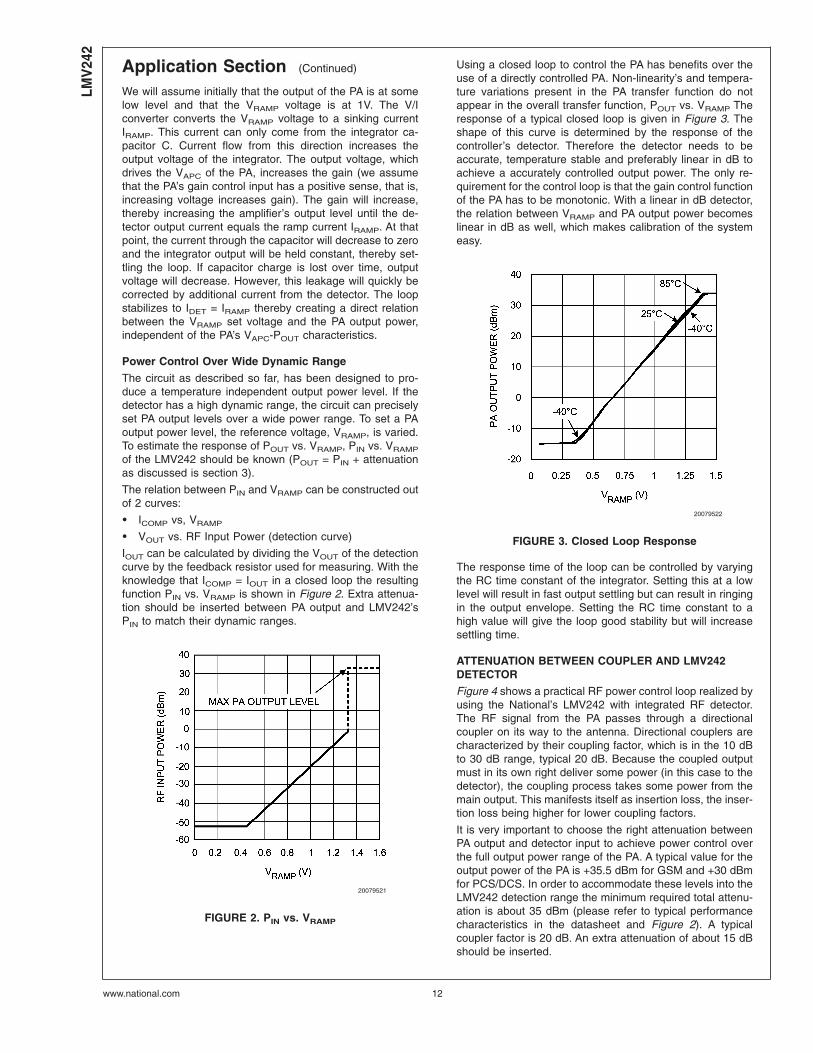
Using a closed loop to control the PA has benefits over theuse of a directly controlled PA. Non-linearity’s and tempera-ture variations present in the PA transfer function do notappear in the overall transfer function, POUT vs. VRAMP Theresponse of a typical closed loop is given in Figure 3. Theshape of this curve is determined by the response of thecontroller’s detector. Therefore the detector needs to beaccurate, temperature stable and preferably linear in dB toachieve a accurately controlled output power. The only re-quirement for the control loop is that the gain control functionof the PA has to be monotonic. With a linear in dB detector,the relation between VRAMP and PA output power becomeslinear in dB as well, which makes calibration of the systemeasy.
The response time of the loop can be controlled by varyingthe RC time constant of the integrator. Setting this at a lowlevel will result in fast output settling but can result in ringingin the output envelope. Setting the RC time constant to ahigh value will give the loop good stability but will increasesettling time.
ATTENUATION BETWEEN COUPLER AND LMV242DETECTOR
Figure 4 shows a practical RF power control loop realized byusing the National’s LMV242 with integrated RF detector.The RF signal from the PA passes through a directionalcoupler on its way to the antenna. Directional couplers arecharacterized by their coupling factor, which is in the 10 dBto 30 dB range, typical 20 dB. Because the coupled outputmust in its own right deliver some power (in this case to thedetector), the coupling process takes some power from themain output. This manifests itself as insertion loss, the inser-tion loss being higher for lower coupling factors.
It is very important to choose the right attenuation betweenPA output and detector input to achieve power control overthe full output power range of the PA. A typical value for theoutput power of the PA is +35.5 dBm for GSM and +30 dBmfor PCS/DCS. In order to accommodate these levels into theLMV242 detection range the minimum required total attenu-ation is about 35 dBm (please refer to typical performancecharacteristics in the datasheet and Figure 2). A typicalcoupler factor is 20 dB. An extra attenuation of about 15 dBshould be inserted.
20079521
FIGURE 2. PIN vs. VRAMP
20079522
FIGURE 3. Closed Loop Response
LMV
242
www.national.com 12
Application Section (Continued)
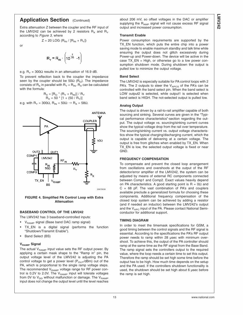
Extra attenuation Z between the coupler and the RF input ofthe LMV242 can be achieved by 2 resistors RX and RY
according to Figure 3, where
Z = 20 LOG (RIN / [RIN + RY])
or
e.g. RY = 300Ω results in an attenuation of 16.9 dB.
To prevent reflection back to the coupler the impedanceseen by the coupler should be 50Ω (RO). The impedanceconsists of RX in parallel with RY + RIN. RX can be calculatedwith the formula:
RX = [RO * (RY + RIN)] / RY
RX = 50 * [1 + (50 / RY)]
e.g. with RY = 300Ω, RIN = 50Ω → RX = 58Ω.
BASEBAND CONTROL OF THE LMV242
The LMV242 has 3 baseband-controlled inputs:
• VRAMP signal (Base band DAC ramp signal)
• TX_EN is a digital signal (performs the function“Shutdown/Transmit Enable”).
• Band Select (BS)
VRAMP Signal
The actual VRAMP input value sets the RF output power. Byapplying a certain mask shape to the “Ramp in” pin, theoutput voltage level of the LMV242 is adjusting the PAcontrol voltage to get a power level (POUT/dBm) out of thePA, which is proportional to the single ramp voltage steps.The recommended VRAMP voltage range for RF power con-trol is 0.2V to 2.0V. The VRAMP input will tolerate voltagesfrom 0V to VDD without malfunction or damage. The VRAMP
input does not change the output level until the level reaches
about 206 mV, so offset voltages in the DAC or amplifiersupplying the RAMP signal will not cause excess RF signaloutput and increased power consumption.
Transmit Enable
Power consumption requirements are supported by theTX_EN function, which puts the entire chip into a powersaving mode to enable maximum standby and talk time whileensuring the output does not glitch excessively duringPower-up and Power-down. The device will be active in thecase TX_EN = High, or otherwise go to a low power con-sumption shutdown mode. During shutdown the output ispulled low to minimize the output voltage.
Band Select
The LMV242 is especially suitable for PA control loops with 2PA’s. The 2 outputs to steer the VAPCS of the PA’s can becontrolled with the band select pin. When the band select isLOW output2 is selected, while output1 is selected whenband select is HIGH. The not-selected output is pulled low.
Analog Output
The output is driven by a rail-to-rail amplifier capable of bothsourcing and sinking. Several curves are given in the “Typi-cal performance characteristics”-section regarding the out-put. The output voltage vs. sourcing/sinking current curvesshow the typical voltage drop from the rail over temperature.The sourcing/sinking current vs. output voltage characteris-tics show the typical charging/discharging current, which theoutput is capable of delivering at a certain voltage. Theoutput is free from glitches when enabled by TX_EN. WhenTX_EN is low, the selected output voltage is fixed or nearGND.
FREQUENCY COMPENSATION
To compensate and prevent the closed loop arrangementfrom oscillations and overshoots at the output of the RFdetector/error amplifier of the LMV242, the system can beadjusted by means of external RC components connectedbetween Comp1 and Comp2. Exact values heavily dependon PA characteristics. A good starting point is R = 0Ω andC = 68 pF. The vast combination of PA’s and couplersavailable preclude a generalized formula for choosing thesecomponents. Additional frequency compensation of theclosed loop system can be achieved by adding a resistor(and if needed an inductor) between the LMV242’s outputand the VAPC input of the PA. Please contact National Semi-conductor for additional support.
TIMING DIAGRAM
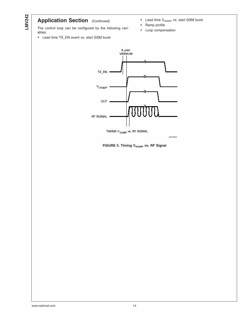
In order to meet the timemask specifications for GSM, agood timing between the control signals and the RF signal isessential. According to the specifications the PA’s RF outputpower needs to ramp within 28 µsec with minimum over-shoot. To achieve this, the output of the PA controller shouldramp at the same time as the RF signal from the Base Band.The ramp signal sets the controllers output to the requiredvalue, where the loop needs a certain time to set this output.Therefore the ramp should be set high some time before theoutput has to be high. How much time depends on the setupand the PA used. If the controllers shutdown functionality isused, the shutdown should be set high about 6 µsec beforethe ramp is set high.
20079530
FIGURE 4. Simplified PA Control Loop with ExtraAttenuation
LMV
242
www.national.com13
Application Section (Continued)
The control loop can be configured by the following vari-ables:
• Lead time TX_EN event vs. start GSM burst
• Lead time VRAMP vs. start GSM burst
• Ramp profile
• Loop compensation
20079531
FIGURE 5. Timing VRAMP vs. RF Signal
LMV
242
www.national.com 14
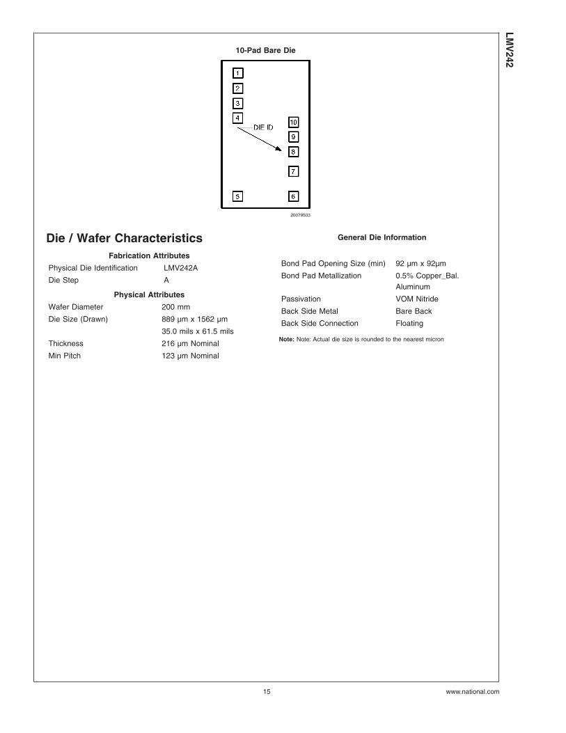
10-Pad Bare Die
20079503
Die / Wafer CharacteristicsFabrication Attributes
Physical Die Identification LMV242A
Die Step A
Physical Attributes
Wafer Diameter 200 mm
Die Size (Drawn) 889 µm x 1562 µm
35.0 mils x 61.5 mils
Thickness 216 µm Nominal
Min Pitch 123 µm Nominal
General Die Information
Bond Pad Opening Size (min) 92 µm x 92µm
Bond Pad Metallization 0.5% Copper_Bal.Aluminum
Passivation VOM Nitride
Back Side Metal Bare Back
Back Side Connection Floating
Note: Note: Actual die size is rounded to the nearest micron
LMV
242
www.national.com15
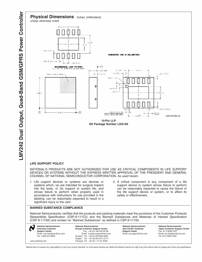
Physical Dimensions inches (millimeters)unless otherwise noted
10-Pin LLPNS Package Number LDA10A
LIFE SUPPORT POLICY
NATIONAL’S PRODUCTS ARE NOT AUTHORIZED FOR USE AS CRITICAL COMPONENTS IN LIFE SUPPORTDEVICES OR SYSTEMS WITHOUT THE EXPRESS WRITTEN APPROVAL OF THE PRESIDENT AND GENERALCOUNSEL OF NATIONAL SEMICONDUCTOR CORPORATION. As used herein:
1. Life support devices or systems are devices orsystems which, (a) are intended for surgical implantinto the body, or (b) support or sustain life, andwhose failure to perform when properly used inaccordance with instructions for use provided in thelabeling, can be reasonably expected to result in asignificant injury to the user.
2. A critical component is any component of a lifesupport device or system whose failure to performcan be reasonably expected to cause the failure ofthe life support device or system, or to affect itssafety or effectiveness.
BANNED SUBSTANCE COMPLIANCE
National Semiconductor certifies that the products and packing materials meet the provisions of the Customer ProductsStewardship Specification (CSP-9-111C2) and the Banned Substances and Materials of Interest Specification(CSP-9-111S2) and contain no ‘‘Banned Substances’’ as defined in CSP-9-111S2.
National SemiconductorAmericas CustomerSupport CenterEmail: [email protected]: 1-800-272-9959
National SemiconductorEurope Customer Support Center
Fax: +49 (0) 180-530 85 86Email: [email protected]
Deutsch Tel: +49 (0) 69 9508 6208English Tel: +44 (0) 870 24 0 2171Français Tel: +33 (0) 1 41 91 8790
National SemiconductorAsia Pacific CustomerSupport CenterEmail: [email protected]
National SemiconductorJapan Customer Support CenterFax: 81-3-5639-7507Email: [email protected]: 81-3-5639-7560
www.national.com
LMV
242
Dua
lOut
put,
Qua
d-B
and
GS
M/G
PR
SP
ower
Con
trol
ler
National does not assume any responsibility for use of any circuitry described, no circuit patent licenses are implied and National reserves the right at any time without notice to change said circuitry and specifications.


![PRELIMINARY DATA SHEET SKY77336 Power Amplifier · PDF fileSKY77336 POWER AMPLIFIER MODULE FOR QUAD-BAND PRELIMINARY DATASHEET GSM / GPRS Skyworks Solutions, Inc. • Phone [781] 376-3000](https://img.pdfslide.net/doc/110x75/5ab9e9487f8b9ad5338e8283/preliminary-data-sheet-sky77336-power-amplifier-power-amplifier-module-for-quad-band.jpg)