Embed Size (px)
Citation preview
Charles Kime & Thomas Kaminski
© 2008 Pearson Education, Inc.(Hyperlinks are active in View Show mode)
Chapter 2 – Combinational Logic Circuits
Part 3 – Additional Gates and Circuits
Logic and Computer Design Fundamentals
Chapter 2 - Part 3 2
Overview
Part 1 – Gate Circuits and Boolean Equations• Binary Logic and Gates
• Boolean Algebra
• Standard Forms
Part 2 – Circuit Optimization• Two-Level Optimization
• Map Manipulation
• Practical Optimization (Espresso)
• Multi-Level Circuit Optimization
Part 3 – Additional Gates and Circuits• Other Gate Types
• Exclusive-OR Operator and Gates
• High-Impedance Outputs
Chapter 2 - Part 3 3
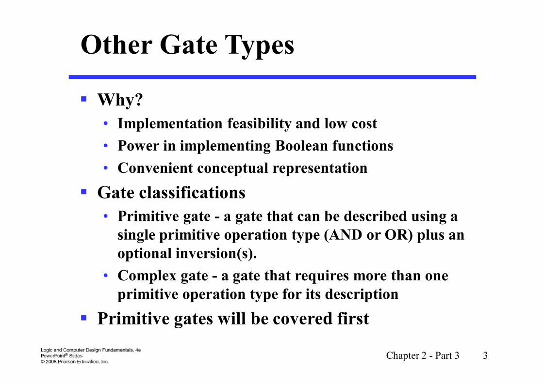
Other Gate Types
Why?
• Implementation feasibility and low cost
• Power in implementing Boolean functions
• Convenient conceptual representation
Gate classifications
• Primitive gate - a gate that can be described using a single primitive operation type (AND or OR) plus an optional inversion(s).
• Complex gate - a gate that requires more than one primitive operation type for its description
Primitive gates will be covered first
Chapter 2 - Part 3 4
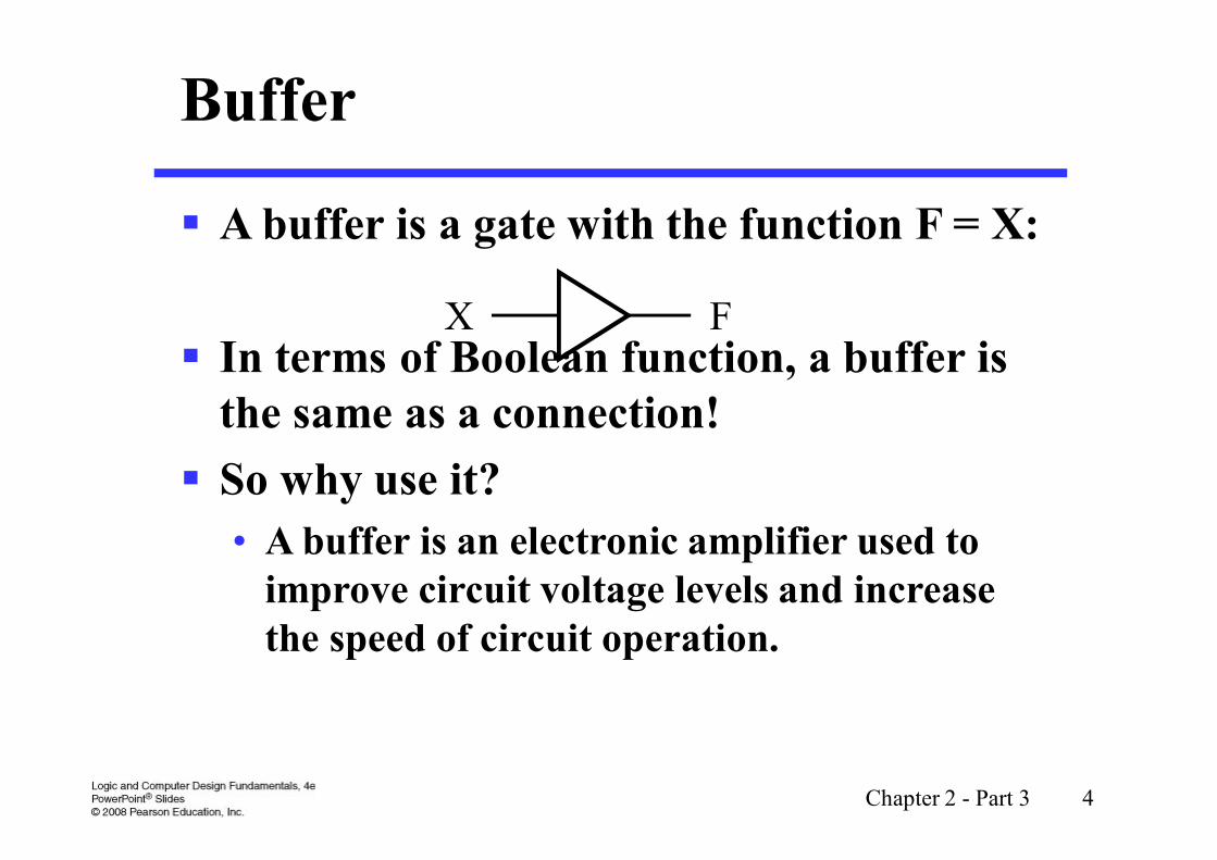
Buffer
A buffer is a gate with the function F = X:
In terms of Boolean function, a buffer is the same as a connection!
So why use it?
• A buffer is an electronic amplifier used to improve circuit voltage levels and increase the speed of circuit operation.
X F
Chapter 2 - Part 3 5
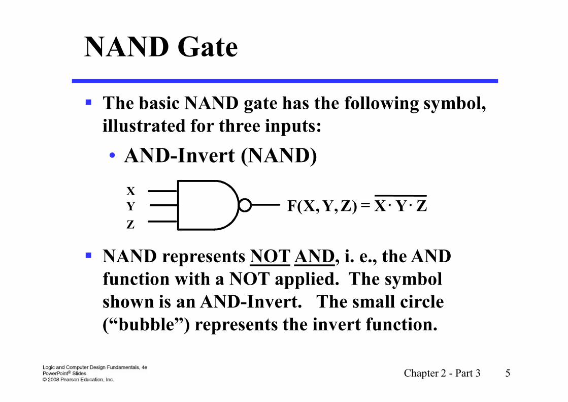
NAND Gate
The basic NAND gate has the following symbol, illustrated for three inputs:
• AND-Invert (NAND)
NAND represents NOT AND, i. e., the AND function with a NOT applied. The symbol shown is an AND-Invert. The small circle (“bubble”) represents the invert function.
X
Y
Z
ZYX)Z,Y,X(F =
Chapter 2 - Part 3 6
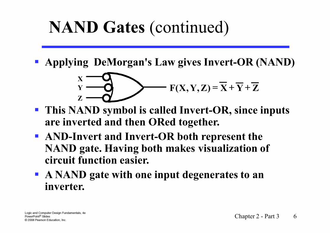
NAND Gates (continued)
Applying DeMorgan's Law gives Invert-OR (NAND)
This NAND symbol is called Invert-OR, since inputs are inverted and then ORed together.
AND-Invert and Invert-OR both represent the NAND gate. Having both makes visualization of circuit function easier.
A NAND gate with one input degenerates to an inverter.
X
Y
Z
ZYX)Z,Y,X(F ++=
Chapter 2 - Part 3 7
NAND Gates (continued)
The NAND gate is the natural implementation for CMOS technology in terms of chip area and speed.
Universal gate - a gate type that can implement any Boolean function.
The NAND gate is a universal gate as shown in Figure 2-24 of the text.
NAND usually does not have a operation symbol defined since• the NAND operation is not associative, and
• we have difficulty dealing with non-associative mathematics!
Chapter 2 - Part 3 8
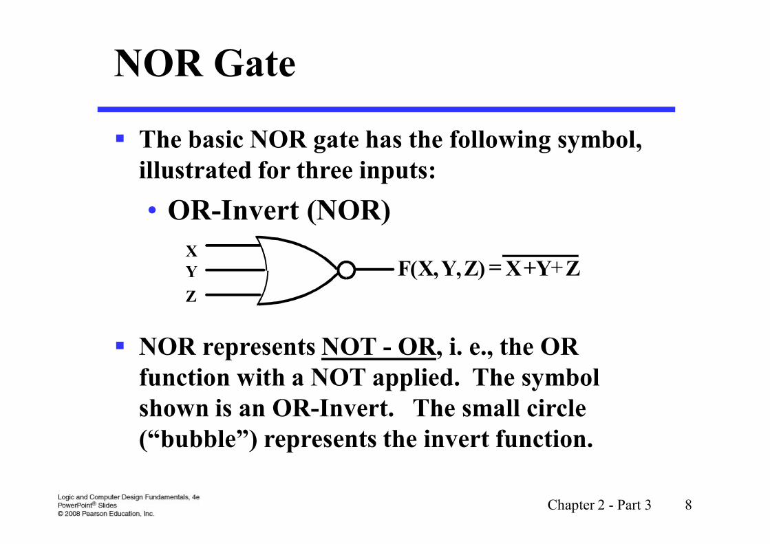
NOR Gate
The basic NOR gate has the following symbol, illustrated for three inputs:
• OR-Invert (NOR)
NOR represents NOT - OR, i. e., the OR function with a NOT applied. The symbol shown is an OR-Invert. The small circle (“bubble”) represents the invert function.
X
Y
Z
ZYX)Z,Y,X(F ++=
Chapter 2 - Part 3 9
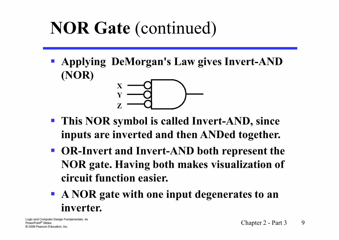
NOR Gate (continued)
Applying DeMorgan's Law gives Invert-AND (NOR)
This NOR symbol is called Invert-AND, since inputs are inverted and then ANDed together.
OR-Invert and Invert-AND both represent the NOR gate. Having both makes visualization of circuit function easier.
A NOR gate with one input degenerates to an inverter.
X
Y
Z
Chapter 2 - Part 3 10
NOR Gate (continued)
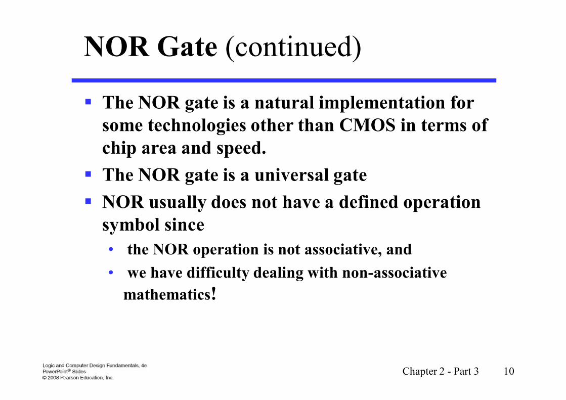
The NOR gate is a natural implementation for some technologies other than CMOS in terms of chip area and speed.
The NOR gate is a universal gate
NOR usually does not have a defined operation symbol since
• the NOR operation is not associative, and
• we have difficulty dealing with non-associative
mathematics!
Chapter 2 - Part 3 11
Exclusive OR/ Exclusive NOR
The eXclusive OR (XOR) function is an important Boolean function used extensively in logic circuits.
The XOR function may be;
• implemented directly as an electronic circuit (truly a gate) or
• implemented by interconnecting other gate types (used as a convenient representation)
The eXclusive NOR function is the complement of the XOR function
By our definition, XOR and XNOR gates are complex gates.
Chapter 2 - Part 3 12
Exclusive OR/ Exclusive NOR
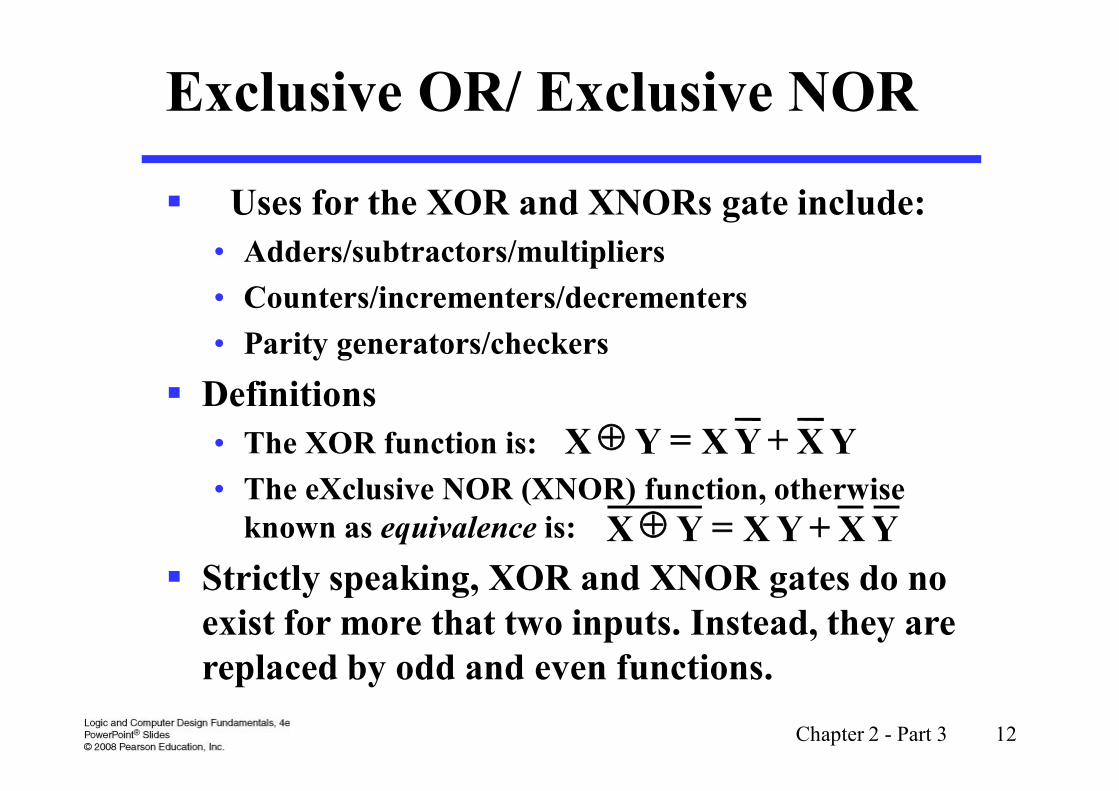
Uses for the XOR and XNORs gate include:
• Adders/subtractors/multipliers
• Counters/incrementers/decrementers
• Parity generators/checkers
Definitions
• The XOR function is:
• The eXclusive NOR (XNOR) function, otherwise known as equivalence is:
Strictly speaking, XOR and XNOR gates do no exist for more that two inputs. Instead, they are replaced by odd and even functions.
YXYXYX +=
YXYXYX +=
Chapter 2 - Part 3 13
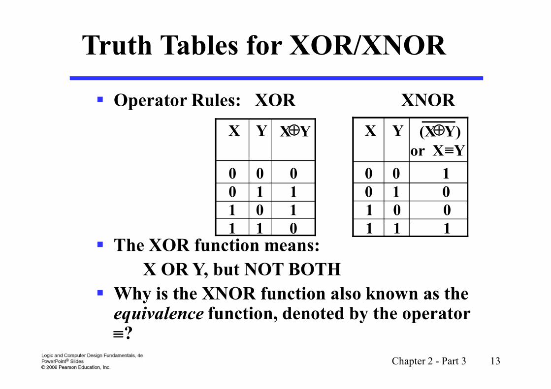
Truth Tables for XOR/XNOR
Operator Rules: XOR XNOR
The XOR function means:
X OR Y, but NOT BOTH
Why is the XNOR function also known as the equivalence function, denoted by the operator ?
X Y XY
0 0 00 1 11 0 11 1 0
X Y
0 0 10 1 01 0 01 1 1
or XY(XY)
Chapter 2 - Part 3 14
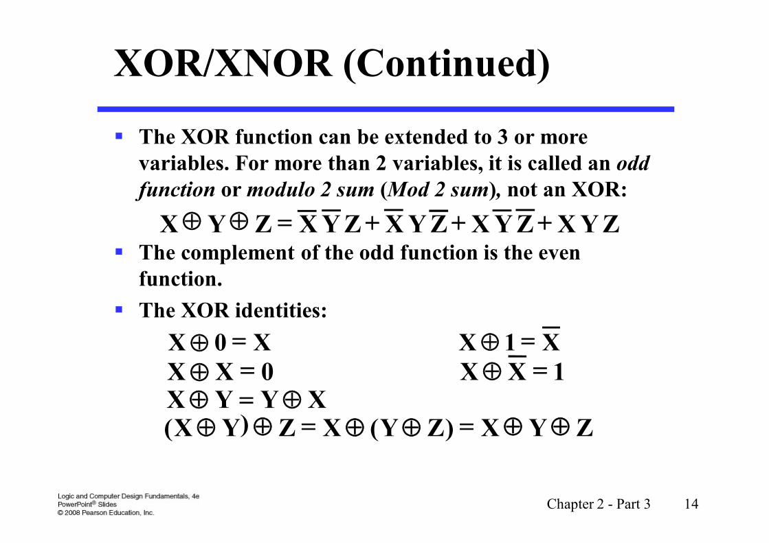
XOR/XNOR (Continued)
The XOR function can be extended to 3 or more variables. For more than 2 variables, it is called an odd function or modulo 2 sum (Mod 2 sum), not an XOR:
The complement of the odd function is the even function.
The XOR identities:
== X1XX0X 1XX0XX ==
XYYX =ZYX)ZY(XZ)YX( ==
+++= ZYXZYXZYXZYXZYX
Chapter 2 - Part 3 15
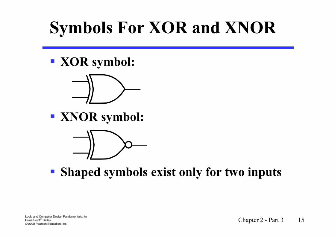
Symbols For XOR and XNOR
XOR symbol:
XNOR symbol:
Shaped symbols exist only for two inputs
Chapter 2 - Part 3 16
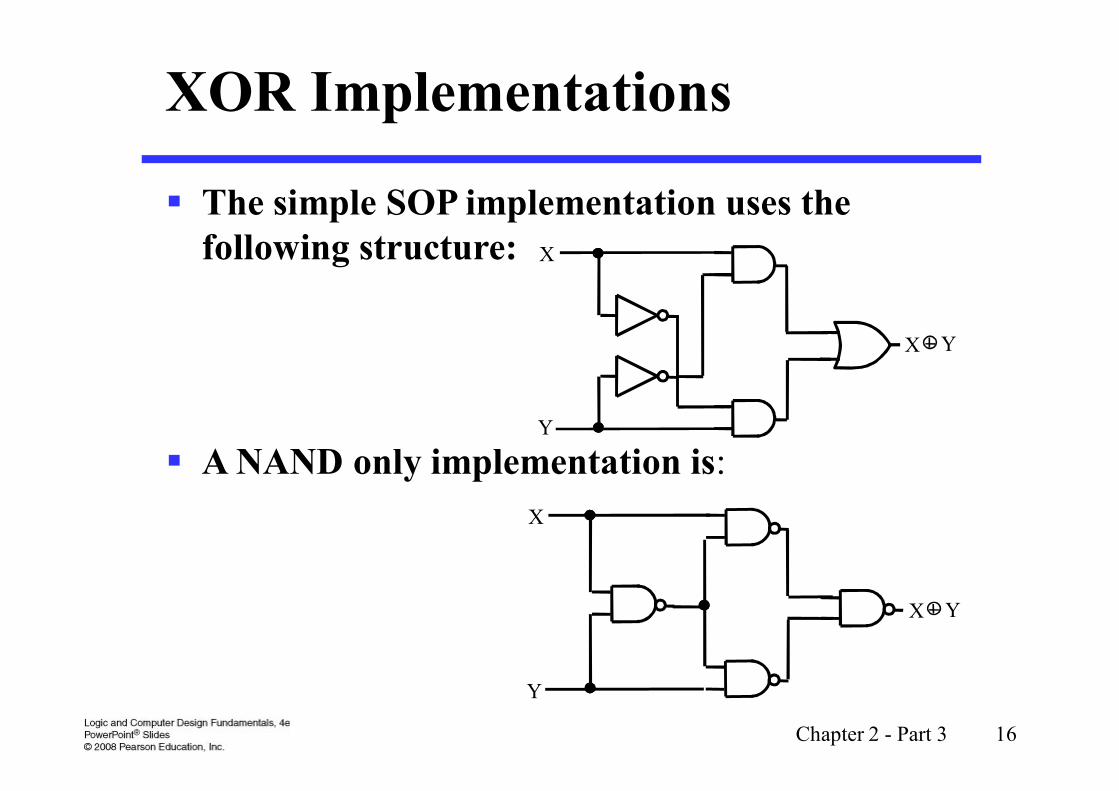
XOR Implementations
The simple SOP implementation uses the following structure:
A NAND only implementation is:
X
Y
X Y
X
Y
X Y
Chapter 2 - Part 3 17
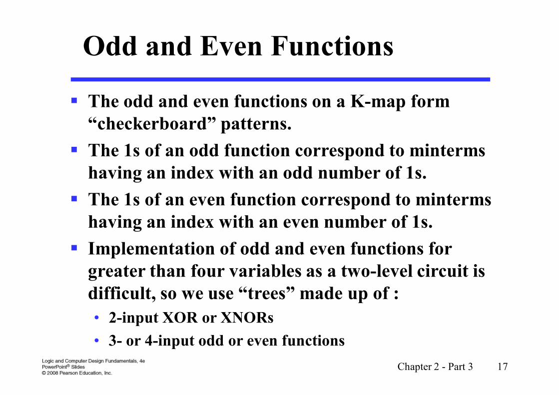
Odd and Even Functions
The odd and even functions on a K-map form “checkerboard” patterns.
The 1s of an odd function correspond to minterms having an index with an odd number of 1s.
The 1s of an even function correspond to minterms having an index with an even number of 1s.
Implementation of odd and even functions for greater than four variables as a two-level circuit is difficult, so we use “trees” made up of :
• 2-input XOR or XNORs
• 3- or 4-input odd or even functions
Chapter 2 - Part 3 18
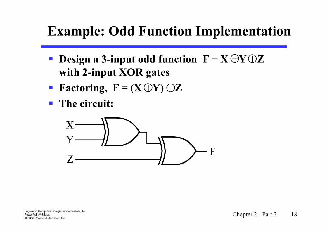
Example: Odd Function Implementation
Design a 3-input odd function F = X Y Zwith 2-input XOR gates
Factoring, F = (X Y) Z
The circuit:
+ +
+ +
X
Y
ZF
Chapter 2 - Part 3 19
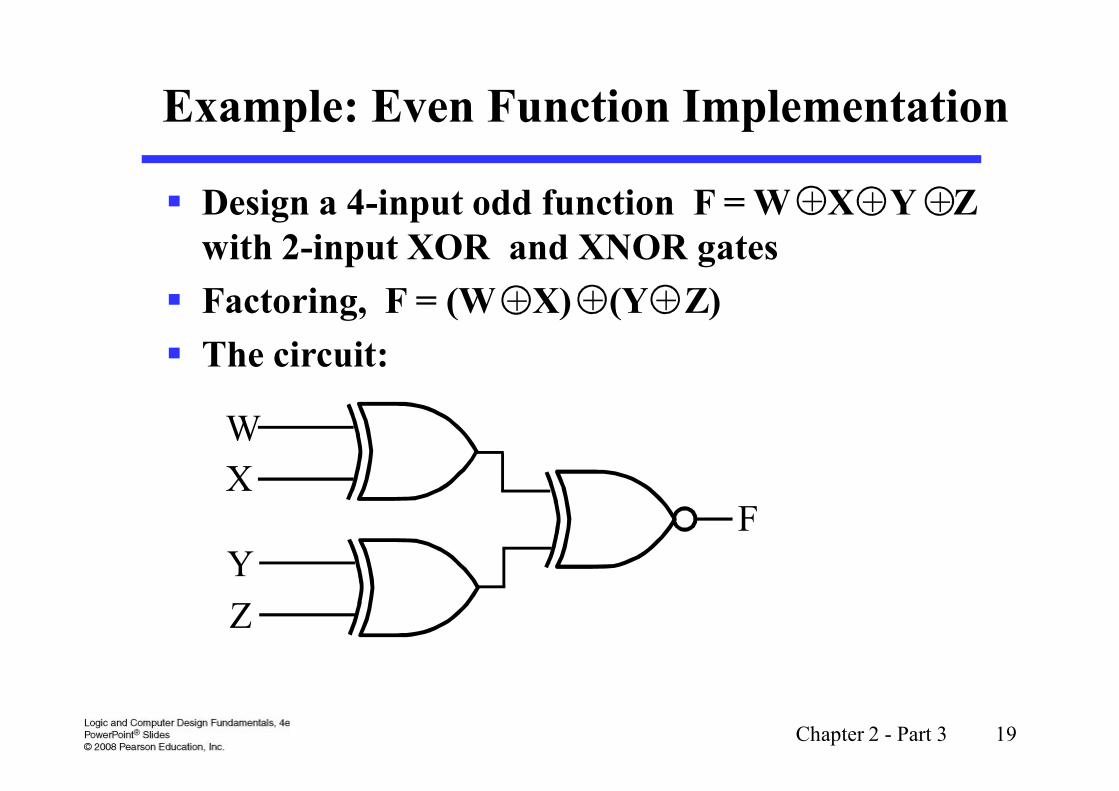
Example: Even Function Implementation
Design a 4-input odd function F = W X Y Zwith 2-input XOR and XNOR gates
Factoring, F = (W X) (Y Z)
The circuit:
+ + +
+ + +
W
X
YF
Z
Chapter 2 - Part 3 20
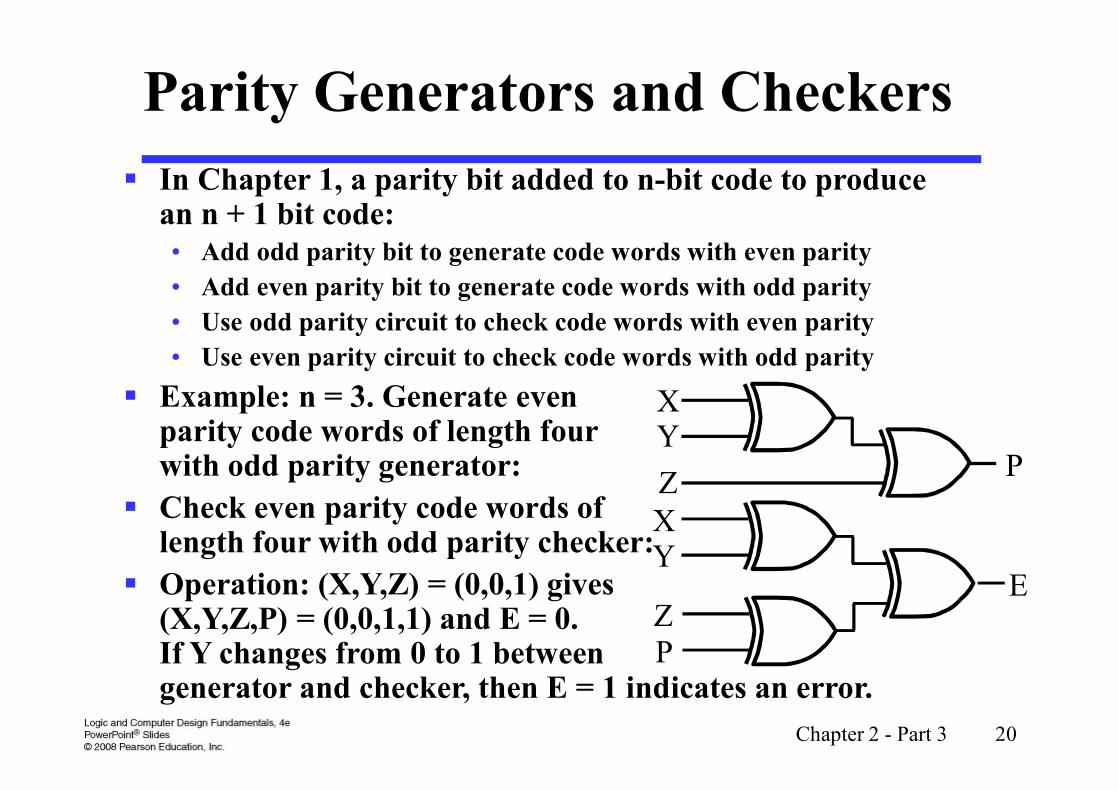
Parity Generators and Checkers
In Chapter 1, a parity bit added to n-bit code to produce an n + 1 bit code:• Add odd parity bit to generate code words with even parity
• Add even parity bit to generate code words with odd parity
• Use odd parity circuit to check code words with even parity
• Use even parity circuit to check code words with odd parity
Example: n = 3. Generate evenparity code words of length fourwith odd parity generator:
Check even parity code words of length four with odd parity checker:
Operation: (X,Y,Z) = (0,0,1) gives(X,Y,Z,P) = (0,0,1,1) and E = 0.If Y changes from 0 to 1 betweengenerator and checker, then E = 1 indicates an error.
XY
ZP
XY
ZE
P
Chapter 2 - Part 3 21
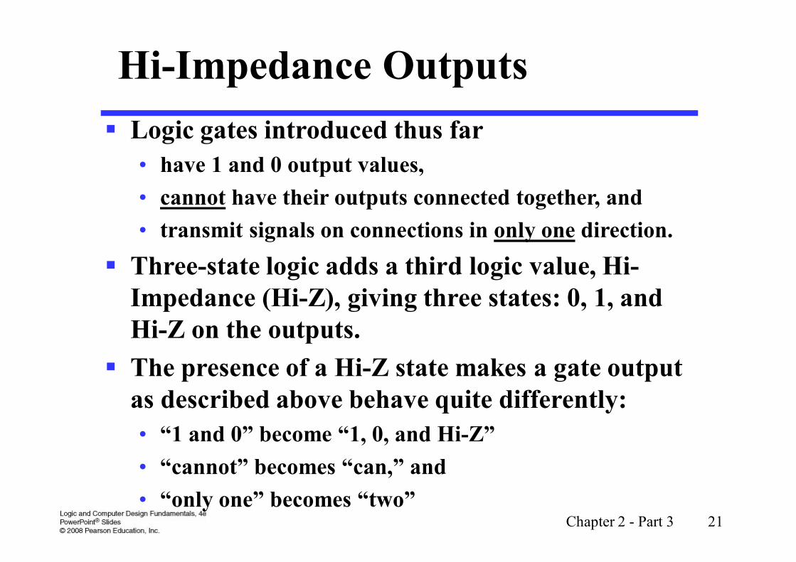
Hi-Impedance Outputs
Logic gates introduced thus far
• have 1 and 0 output values,
• cannot have their outputs connected together, and
• transmit signals on connections in only one direction.
Three-state logic adds a third logic value, Hi-Impedance (Hi-Z), giving three states: 0, 1, and Hi-Z on the outputs.
The presence of a Hi-Z state makes a gate output as described above behave quite differently:
• “1 and 0” become “1, 0, and Hi-Z”
• “cannot” becomes “can,” and
• “only one” becomes “two”
Chapter 2 - Part 3 22
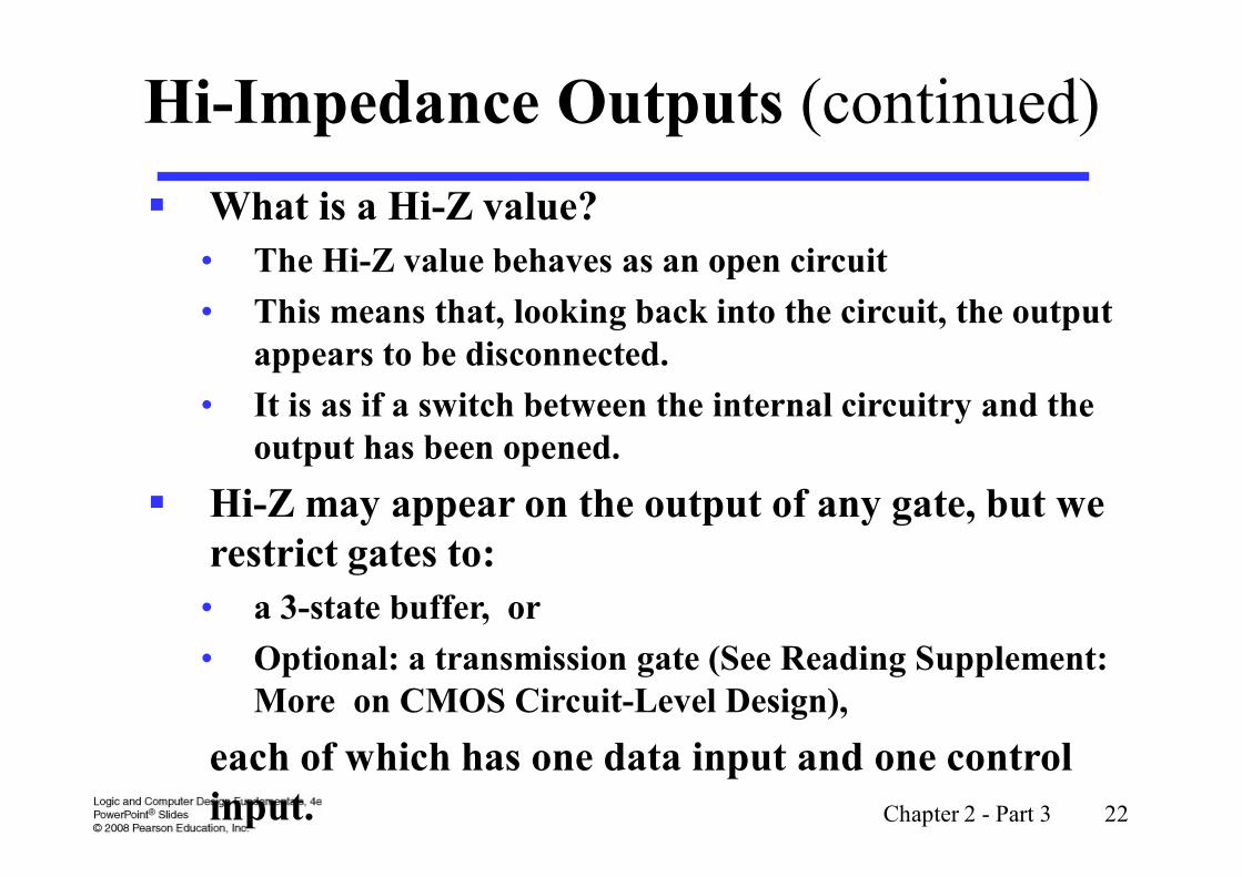
Hi-Impedance Outputs (continued)
What is a Hi-Z value?
• The Hi-Z value behaves as an open circuit
• This means that, looking back into the circuit, the output appears to be disconnected.
• It is as if a switch between the internal circuitry and the output has been opened.
Hi-Z may appear on the output of any gate, but we restrict gates to:
• a 3-state buffer, or
• Optional: a transmission gate (See Reading Supplement: More on CMOS Circuit-Level Design),
each of which has one data input and one control input.
Chapter 2 - Part 3 23
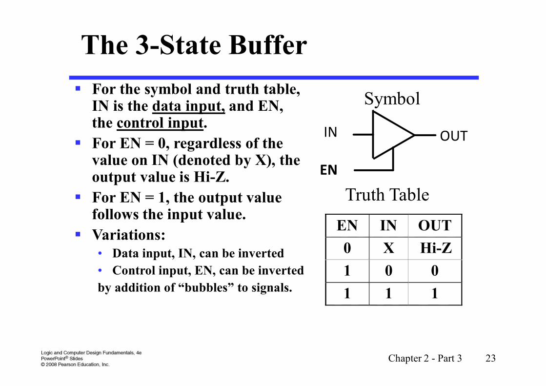
The 3-State Buffer
For the symbol and truth table, IN is the data input, and EN, the control input.
For EN = 0, regardless of the value on IN (denoted by X), the output value is Hi-Z.
For EN = 1, the output value follows the input value.
Variations: • Data input, IN, can be inverted
• Control input, EN, can be inverted
by addition of “bubbles” to signals.
IN
EN
OUT
EN IN OUT
0 X Hi-Z
1 0 0
1 1 1
Symbol
Truth Table
Chapter 2 - Part 3 24
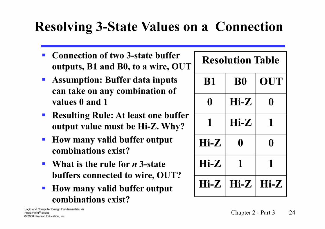
Resolving 3-State Values on a Connection
Connection of two 3-state buffer outputs, B1 and B0, to a wire, OUT
Assumption: Buffer data inputs can take on any combination of values 0 and 1
Resulting Rule: At least one buffer output value must be Hi-Z. Why?
How many valid buffer output combinations exist?
What is the rule for n 3-state buffers connected to wire, OUT?
How many valid buffer output combinations exist?
Resolution Table
B1 B0 OUT
0 Hi-Z 0
1 Hi-Z 1
Hi-Z 0 0
Hi-Z 1 1
Hi-Z Hi-Z Hi-Z
Chapter 2 - Part 3 25
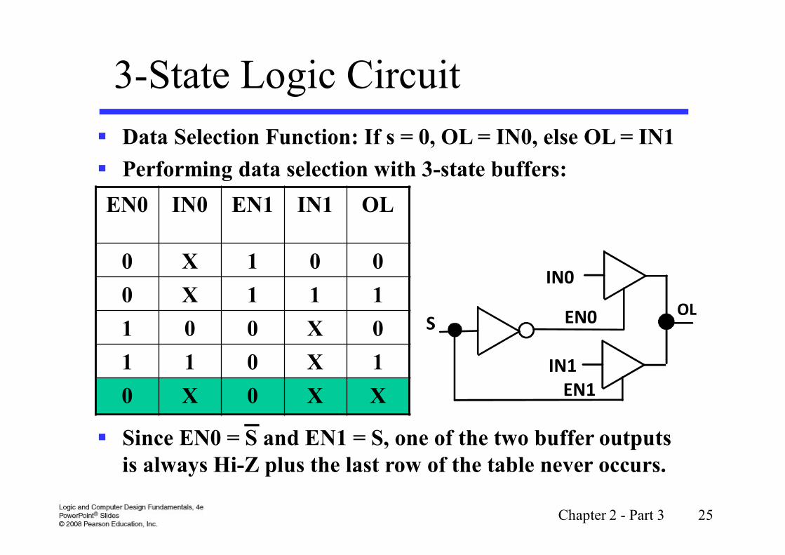
3-State Logic Circuit
Data Selection Function: If s = 0, OL = IN0, else OL = IN1
Performing data selection with 3-state buffers:
Since EN0 = S and EN1 = S, one of the two buffer outputs is always Hi-Z plus the last row of the table never occurs.
IN0
IN1
EN0
EN1
SOL
EN0 IN0 EN1 IN1 OL
0 X 1 0 0
0 X 1 1 1
1 0 0 X 0
1 1 0 X 1
0 X 0 X X
Chapter 2 - Part 3 26
More Complex Gates
The remaining complex gates are SOP or POS structures with and without an output inverter.
The names are derived using:
• A - AND
• O - OR
• I - Inverter
• Numbers of inputs on first-level “gates” or directly to second-level “gates”
Chapter 2 - Part 3 27
More Complex Gates (continued)
Example: AOI - AND-OR-Invert consists of a single gate with AND functions driving an OR function which is inverted.
Example: 2-2-1 AO has two 2-input ANDS driving an OR with one additional OR input
These gate types are used because:
• the number of transistors needed is fewer than required by connecting together primitive gates
• potentially, the circuit delay is smaller, increasing the circuit operating speed
Chapter 2 - Part 3 28
Terms of Use
All (or portions) of this material © 2008 by Pearson Education, Inc.
Permission is given to incorporate this material or adaptations thereof into classroom presentations and handouts to instructors in courses adopting the latest edition of Logic and Computer Design Fundamentals as the course textbook.
These materials or adaptations thereof are not to be sold or otherwise offered for consideration.
This Terms of Use slide or page is to be included within the original materials or any adaptations thereof.