Embed Size (px)
Citation preview
July 2009 Doc ID 7194 Rev 21 1/24
24
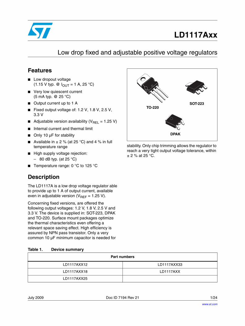
LD1117Axx
Low drop fixed and adjustable positive voltage regulators
Features■ Low dropout voltage
(1.15 V typ. @ IOUT = 1 A, 25 °C)
■ Very low quiescent current(5 mA typ. @ 25 °C)
■ Output current up to 1 A
■ Fixed output voltage of: 1.2 V, 1.8 V, 2.5 V, 3.3 V
■ Adjustable version availability (VREL = 1.25 V)
■ Internal current and thermal limit
■ Only 10 µF for stability
■ Available in ± 2 % (at 25 °C) and 4 % in full temperature range
■ High supply voltage rejection:– 80 dB typ. (at 25 °C)
■ Temperature range: 0 °C to 125 °C
DescriptionThe LD1117A is a low drop voltage regulator able to provide up to 1 A of output current, available even in adjustable version (VREF = 1.25 V).
Concerning fixed versions, are offered the following output voltages: 1.2 V, 1.8 V, 2.5 V and 3.3 V. The device is supplied in: SOT-223, DPAK and TO-220. Surface mount packages optimize the thermal characteristics even offering a relevant space saving effect. High efficiency is assured by NPN pass transistor. Only a very common 10 µF minimum capacitor is needed for
stability. Only chip trimming allows the regulator to reach a very tight output voltage tolerance, within ± 2 % at 25 °C.
SOT-223TO-220
DPAK
Table 1. Device summary
Part numbers
LD1117AXX12 LD1117AXX33
LD1117AXX18 LD1117AXX
LD1117AXX25
www.st.com
Contents LD1117Axx
2/24 Doc ID 7194 Rev 21
Contents
1 Diagram . . . . . . . . . . . . . . . . . . . . . . . . . . . . . . . . . . . . . . . . . . . . . . . . . . . 3
2 Pin configuration . . . . . . . . . . . . . . . . . . . . . . . . . . . . . . . . . . . . . . . . . . . 4
3 Maximum ratings . . . . . . . . . . . . . . . . . . . . . . . . . . . . . . . . . . . . . . . . . . . . 5
4 Schematic application . . . . . . . . . . . . . . . . . . . . . . . . . . . . . . . . . . . . . . . 6
5 Electrical characteristics . . . . . . . . . . . . . . . . . . . . . . . . . . . . . . . . . . . . . 7
6 Typical application . . . . . . . . . . . . . . . . . . . . . . . . . . . . . . . . . . . . . . . . . 12
7 LD1117A adjustable: application note . . . . . . . . . . . . . . . . . . . . . . . . . 15
8 Package mechanical data . . . . . . . . . . . . . . . . . . . . . . . . . . . . . . . . . . . . 16
9 Order codes . . . . . . . . . . . . . . . . . . . . . . . . . . . . . . . . . . . . . . . . . . . . . . 22
10 Revision history . . . . . . . . . . . . . . . . . . . . . . . . . . . . . . . . . . . . . . . . . . . 23
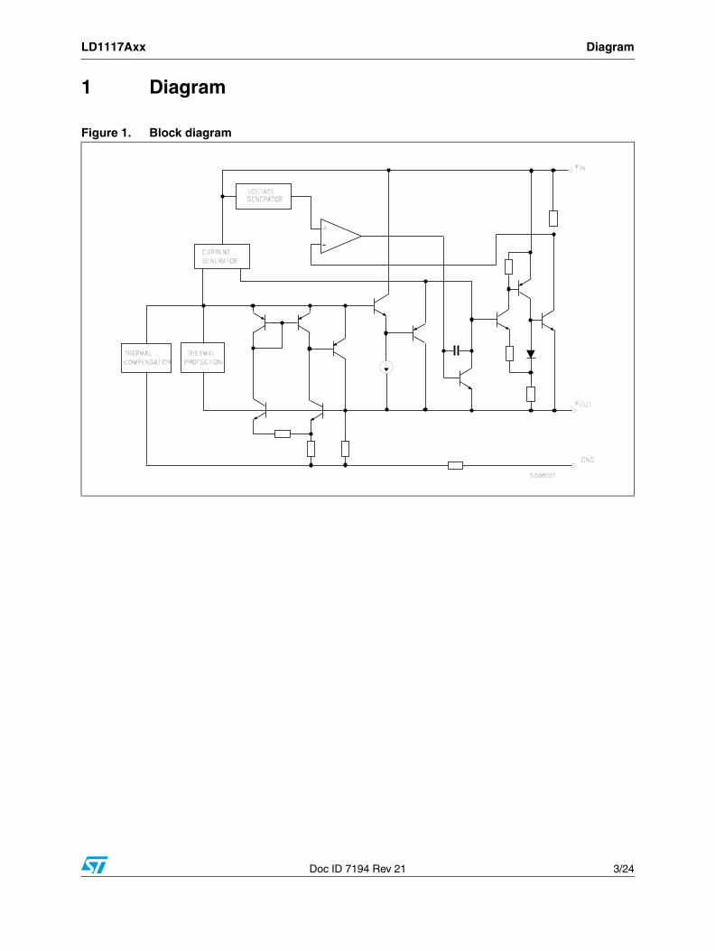
LD1117Axx Diagram
Doc ID 7194 Rev 21 3/24
1 Diagram
Figure 1. Block diagram
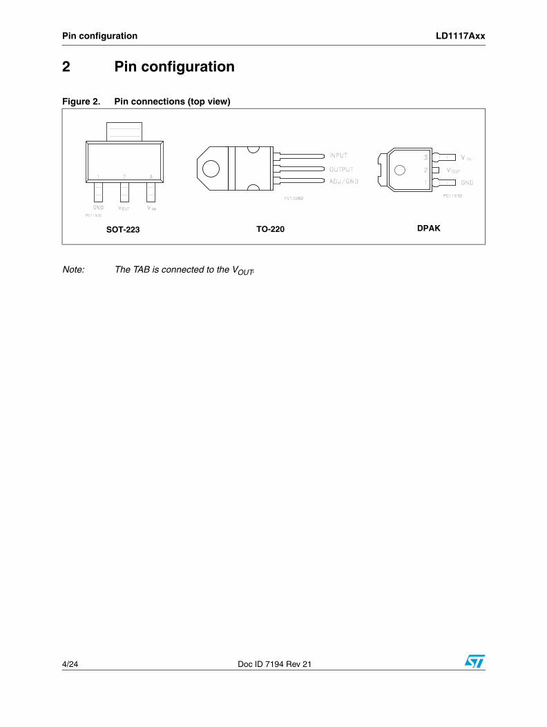
Pin configuration LD1117Axx
4/24 Doc ID 7194 Rev 21
2 Pin configuration
Note: The TAB is connected to the VOUT.
Figure 2. Pin connections (top view)
DPAKSOT-223 TO-220
LD1117Axx Maximum ratings
Doc ID 7194 Rev 21 5/24
3 Maximum ratings
Note: Absolute maximum ratings are those values beyond which damage to the device may occur. Functional operation under these condition is not implied. Over the above suggested max power dissipation a short circuit could definitively damage the device.
Table 2. Absolute maximum ratings
Symbol Parameter Value Unit
VIN DC input voltage 15 V
PD Power dissipation 12 W
TSTG Storage temperature range -40 to +150 °C
TOP Operating junction temperature range 0 to +125 °C
Table 3. Thermal data
Symbol Parameter SOT-223 DPAK TO-220 Unit
RthJC Thermal resistance junction-case 15 8 3 °C/W
RthJA Thermal resistance junction-ambient 50 °C/W
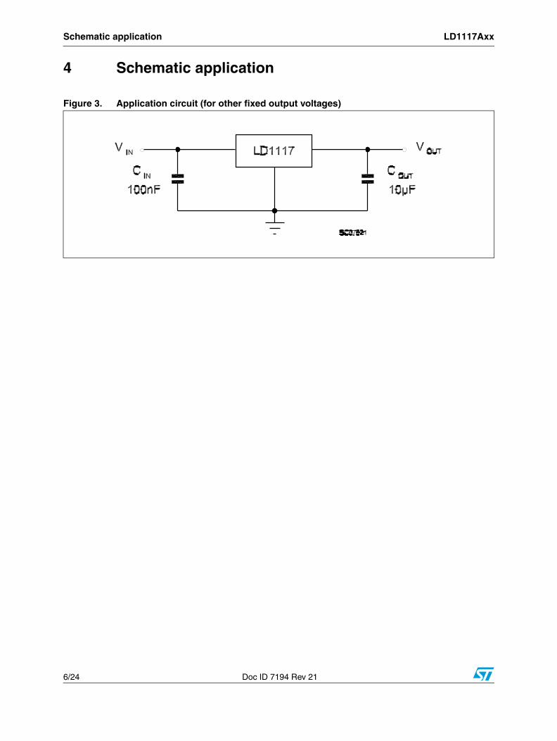
Schematic application LD1117Axx
6/24 Doc ID 7194 Rev 21
4 Schematic application
Figure 3. Application circuit (for other fixed output voltages)
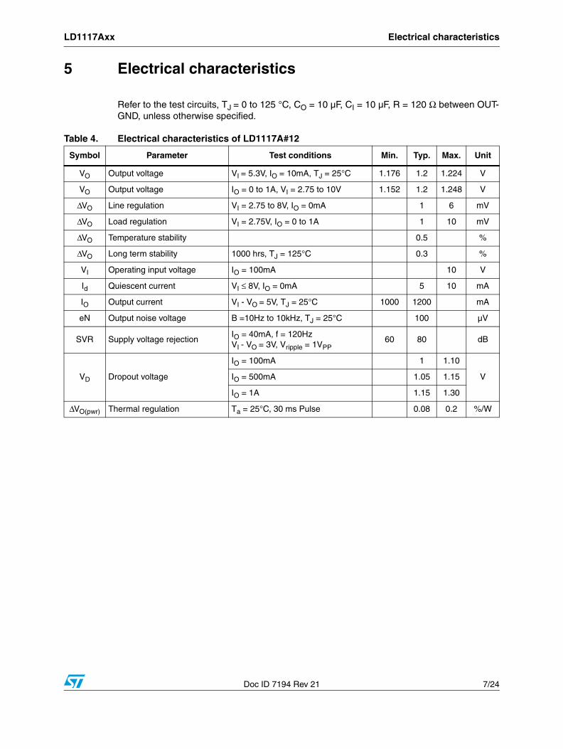
LD1117Axx Electrical characteristics
Doc ID 7194 Rev 21 7/24
5 Electrical characteristics
Refer to the test circuits, TJ = 0 to 125 °C, CO = 10 µF, CI = 10 µF, R = 120 Ω between OUT-GND, unless otherwise specified.
Table 4. Electrical characteristics of LD1117A#12
Symbol Parameter Test conditions Min. Typ. Max. Unit
VO Output voltage VI = 5.3V, IO = 10mA, TJ = 25°C 1.176 1.2 1.224 V
VO Output voltage IO = 0 to 1A, VI = 2.75 to 10V 1.152 1.2 1.248 V
ΔVO Line regulation VI = 2.75 to 8V, IO = 0mA 1 6 mV
ΔVO Load regulation VI = 2.75V, IO = 0 to 1A 1 10 mV
ΔVO Temperature stability 0.5 %
ΔVO Long term stability 1000 hrs, TJ = 125°C 0.3 %
VI Operating input voltage IO = 100mA 10 V
Id Quiescent current VI ≤ 8V, IO = 0mA 5 10 mA
IO Output current VI - VO = 5V, TJ = 25°C 1000 1200 mA
eN Output noise voltage B =10Hz to 10kHz, TJ = 25°C 100 µV
SVR Supply voltage rejectionIO = 40mA, f = 120HzVI - VO = 3V, Vripple = 1VPP
60 80 dB
VD Dropout voltage
IO = 100mA 1 1.10
VIO = 500mA 1.05 1.15
IO = 1A 1.15 1.30
ΔVO(pwr) Thermal regulation Ta = 25°C, 30 ms Pulse 0.08 0.2 %/W
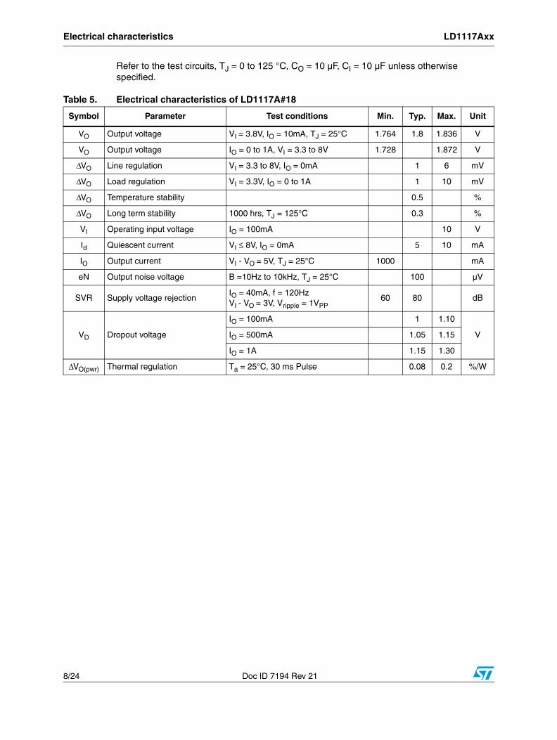
Electrical characteristics LD1117Axx
8/24 Doc ID 7194 Rev 21
Refer to the test circuits, TJ = 0 to 125 °C, CO = 10 µF, CI = 10 µF unless otherwise specified.
Table 5. Electrical characteristics of LD1117A#18
Symbol Parameter Test conditions Min. Typ. Max. Unit
VO Output voltage VI = 3.8V, IO = 10mA, TJ = 25°C 1.764 1.8 1.836 V
VO Output voltage IO = 0 to 1A, VI = 3.3 to 8V 1.728 1.872 V
ΔVO Line regulation VI = 3.3 to 8V, IO = 0mA 1 6 mV
ΔVO Load regulation VI = 3.3V, IO = 0 to 1A 1 10 mV
ΔVO Temperature stability 0.5 %
ΔVO Long term stability 1000 hrs, TJ = 125°C 0.3 %
VI Operating input voltage IO = 100mA 10 V
Id Quiescent current VI ≤ 8V, IO = 0mA 5 10 mA
IO Output current VI - VO = 5V, TJ = 25°C 1000 mA
eN Output noise voltage B =10Hz to 10kHz, TJ = 25°C 100 µV
SVR Supply voltage rejectionIO = 40mA, f = 120HzVI - VO = 3V, Vripple = 1VPP
60 80 dB
VD Dropout voltage
IO = 100mA 1 1.10
VIO = 500mA 1.05 1.15
IO = 1A 1.15 1.30
ΔVO(pwr) Thermal regulation Ta = 25°C, 30 ms Pulse 0.08 0.2 %/W
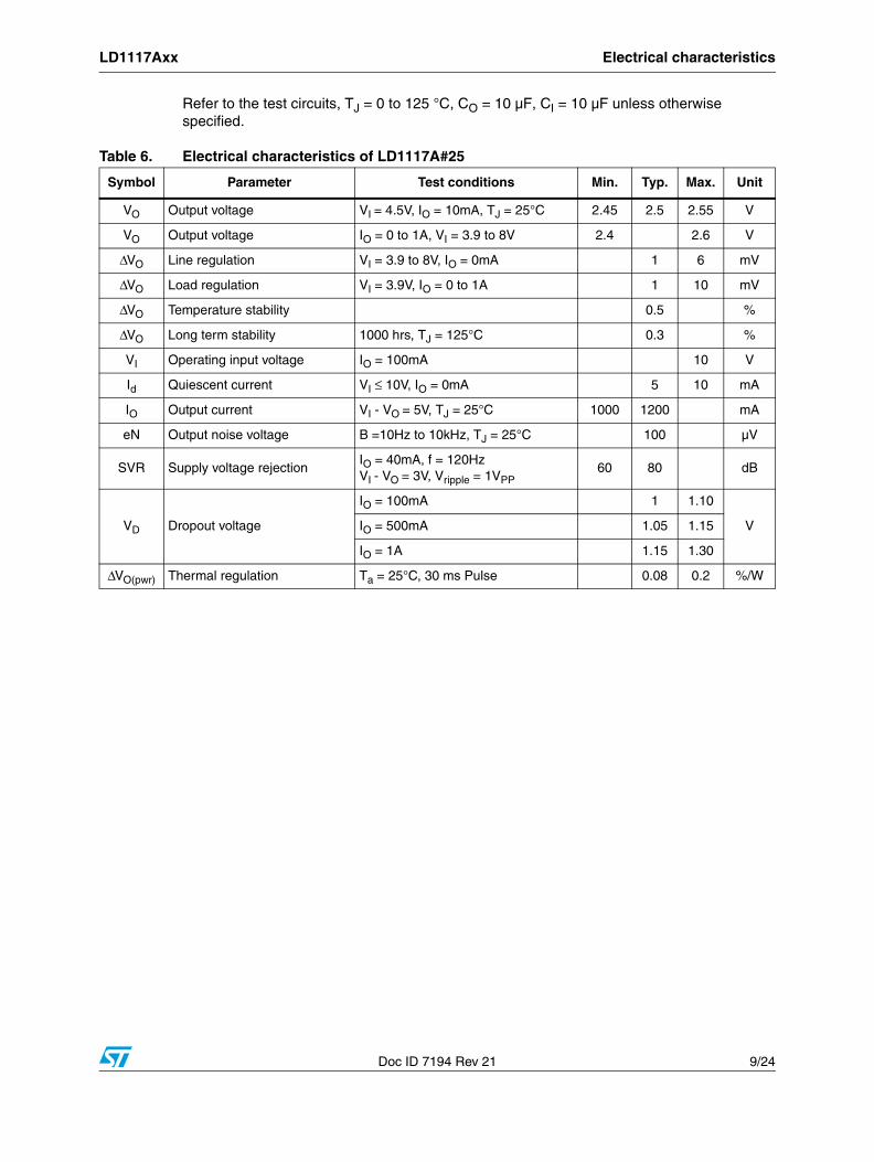
LD1117Axx Electrical characteristics
Doc ID 7194 Rev 21 9/24
Refer to the test circuits, TJ = 0 to 125 °C, CO = 10 µF, CI = 10 µF unless otherwise specified.
Table 6. Electrical characteristics of LD1117A#25
Symbol Parameter Test conditions Min. Typ. Max. Unit
VO Output voltage VI = 4.5V, IO = 10mA, TJ = 25°C 2.45 2.5 2.55 V
VO Output voltage IO = 0 to 1A, VI = 3.9 to 8V 2.4 2.6 V
ΔVO Line regulation VI = 3.9 to 8V, IO = 0mA 1 6 mV
ΔVO Load regulation VI = 3.9V, IO = 0 to 1A 1 10 mV
ΔVO Temperature stability 0.5 %
ΔVO Long term stability 1000 hrs, TJ = 125°C 0.3 %
VI Operating input voltage IO = 100mA 10 V
Id Quiescent current VI ≤ 10V, IO = 0mA 5 10 mA
IO Output current VI - VO = 5V, TJ = 25°C 1000 1200 mA
eN Output noise voltage B =10Hz to 10kHz, TJ = 25°C 100 µV
SVR Supply voltage rejectionIO = 40mA, f = 120HzVI - VO = 3V, Vripple = 1VPP
60 80 dB
VD Dropout voltage
IO = 100mA 1 1.10
VIO = 500mA 1.05 1.15
IO = 1A 1.15 1.30
ΔVO(pwr) Thermal regulation Ta = 25°C, 30 ms Pulse 0.08 0.2 %/W

Electrical characteristics LD1117Axx
10/24 Doc ID 7194 Rev 21
Refer to the test circuits, TJ = 0 to 125 °C, CO = 10 µF, CI = 10 µF unless otherwise specified.
Table 7. Electrical characteristics of LD1117A#33
Symbol Parameter Test conditions Min. Typ. Max. Unit
VO Output voltage VI = 5.3V, IO = 10mA, TJ = 25°C 3.234 3.3 3.366 V
VO Output voltage IO = 0 to 1A, VI = 4.75 to 10V 3.168 3.432 V
ΔVO Line regulation VI = 4.75 to 8V, IO = 0mA 1 6 mV
ΔVO Load regulation VI = 4.75V, IO = 0 to 1A 1 10 mV
ΔVO Temperature stability 0.5 %
ΔVO Long term stability 1000 hrs, TJ = 125°C 0.3 %
VI Operating input voltage IO = 100mA 10 V
Id Quiescent current VI ≤ 10V, IO = 0mA 5 10 mA
IO Output current VI - VO = 5V, TJ = 25°C 1000 1200 mA
eN Output noise voltage B =10Hz to 10kHz, TJ = 25°C 100 µV
SVR Supply voltage rejectionIO = 40mA, f = 120HzVI - VO = 3V, Vripple = 1VPP
60 75 dB
VD Dropout voltage
IO = 100mA 1 1.10
VIO = 500mA 1.05 1.15
IO = 1A 1.15 1.30
ΔVO(pwr) Thermal regulation Ta = 25°C, 30 ms Pulse 0.08 0.2 %/W
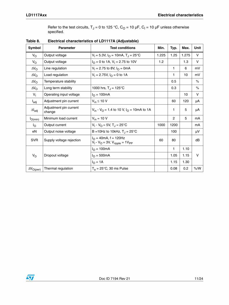
LD1117Axx Electrical characteristics
Doc ID 7194 Rev 21 11/24
Refer to the test circuits, TJ = 0 to 125 °C, CO = 10 µF, CI = 10 µF unless otherwise specified.
Table 8. Electrical characteristics of LD1117A (Adjustable)
Symbol Parameter Test conditions Min. Typ. Max. Unit
VO Output voltage VI = 5.3V, IO = 10mA, TJ = 25°C 1.225 1.25 1.275 V
VO Output voltage IO = 0 to 1A, VI = 2.75 to 10V 1.2 1.3 V
ΔVO Line regulation VI = 2.75 to 8V, IO = 0mA 1 6 mV
ΔVO Load regulation VI = 2.75V, IO = 0 to 1A 1 10 mV
ΔVO Temperature stability 0.5 %
ΔVO Long term stability 1000 hrs, TJ = 125°C 0.3 %
VI Operating input voltage IO = 100mA 10 V
Iadj Adjustment pin current Vin ≤ 10 V 60 120 µA
ΔIadjAdjustment pin current change
Vin - VO = 1.4 to 10 V, IO = 10mA to 1A 1 5 µA
IO(min) Minimum load current Vin = 10 V 2 5 mA
IO Output current VI - VO = 5V, TJ = 25°C 1000 1200 mA
eN Output noise voltage B =10Hz to 10kHz, TJ = 25°C 100 µV
SVR Supply voltage rejectionIO = 40mA, f = 120HzVI - VO = 3V, Vripple = 1VPP
60 80 dB
VD Dropout voltage
IO = 100mA 1 1.10
VIO = 500mA 1.05 1.15
IO = 1A 1.15 1.30
ΔVO(pwr) Thermal regulation Ta = 25°C, 30 ms Pulse 0.08 0.2 %/W
Typical application LD1117Axx
12/24 Doc ID 7194 Rev 21
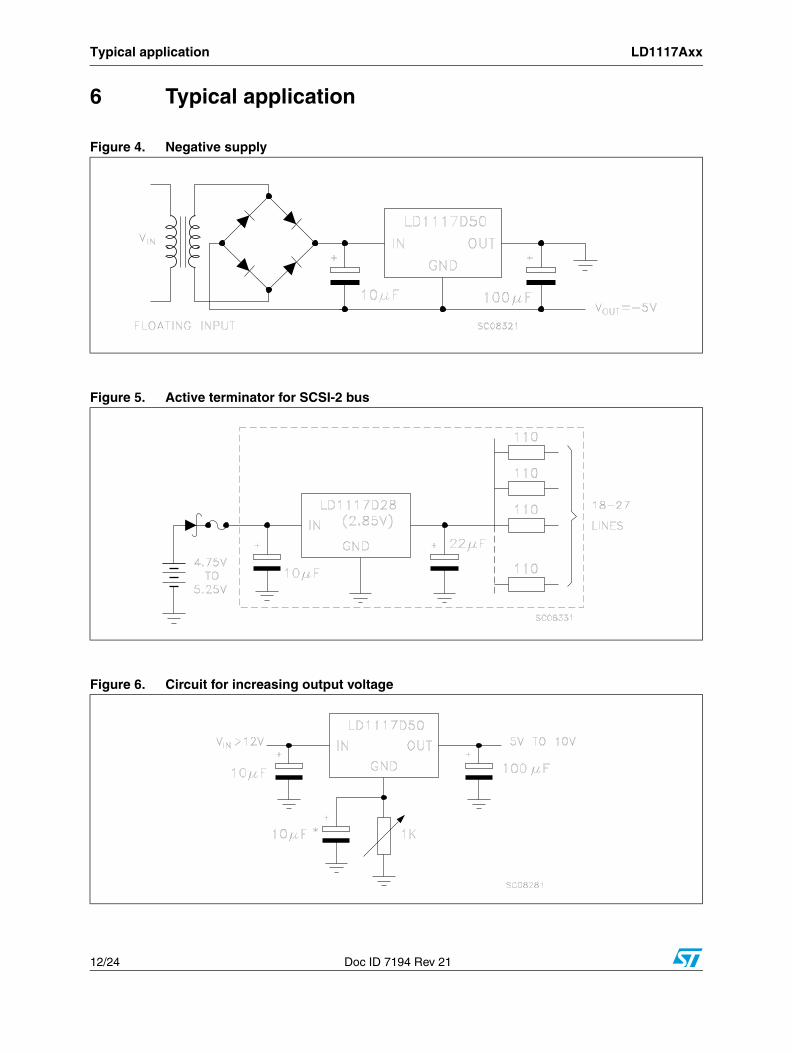
6 Typical application
Figure 4. Negative supply
Figure 5. Active terminator for SCSI-2 bus
Figure 6. Circuit for increasing output voltage
LD1117Axx Typical application
Doc ID 7194 Rev 21 13/24
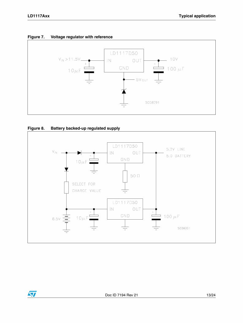
Figure 7. Voltage regulator with reference
Figure 8. Battery backed-up regulated supply
Typical application LD1117Axx
14/24 Doc ID 7194 Rev 21
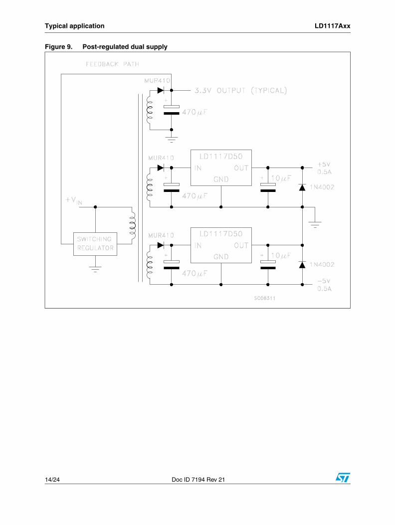
Figure 9. Post-regulated dual supply
LD1117Axx LD1117A adjustable: application note
Doc ID 7194 Rev 21 15/24
7 LD1117A adjustable: application note
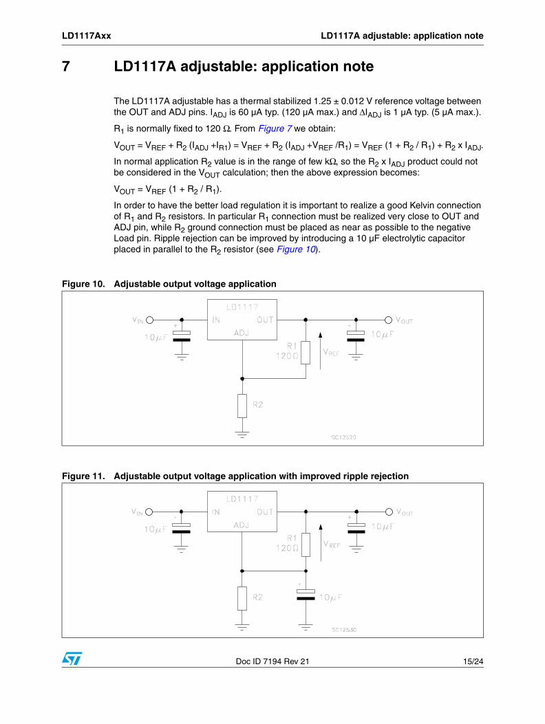
The LD1117A adjustable has a thermal stabilized 1.25 ± 0.012 V reference voltage between the OUT and ADJ pins. IADJ is 60 µA typ. (120 µA max.) and ΔIADJ is 1 µA typ. (5 µA max.).
R1 is normally fixed to 120 Ω. From Figure 7 we obtain:
VOUT = VREF + R2 (IADJ +IR1) = VREF + R2 (IADJ +VREF /R1) = VREF (1 + R2 / R1) + R2 x IADJ.
In normal application R2 value is in the range of few kΩ, so the R2 x IADJ product could not be considered in the VOUT calculation; then the above expression becomes:
VOUT = VREF (1 + R2 / R1).
In order to have the better load regulation it is important to realize a good Kelvin connection of R1 and R2 resistors. In particular R1 connection must be realized very close to OUT and ADJ pin, while R2 ground connection must be placed as near as possible to the negative Load pin. Ripple rejection can be improved by introducing a 10 µF electrolytic capacitor placed in parallel to the R2 resistor (see Figure 10).
Figure 10. Adjustable output voltage application
Figure 11. Adjustable output voltage application with improved ripple rejection
Package mechanical data LD1117Axx
16/24 Doc ID 7194 Rev 21
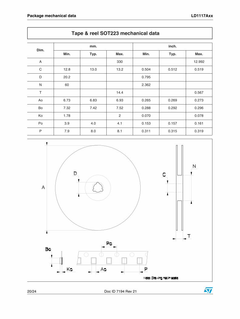
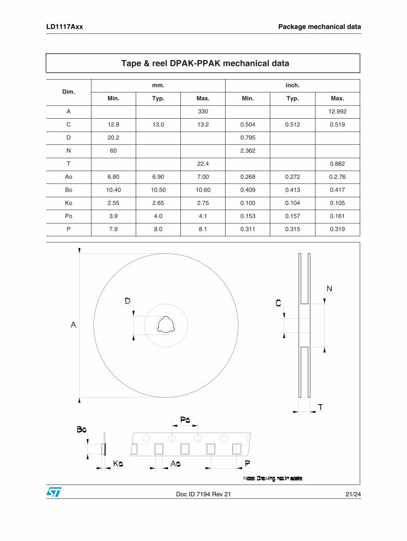
8 Package mechanical data
In order to meet environmental requirements, ST offers these devices in different grades of ECOPACK® packages, depending on their level of environmental compliance. ECOPACK® specifications, grade definitions and product status are available at: www.st.com. ECOPACK® is an ST trademark.
LD1117Axx Package mechanical data
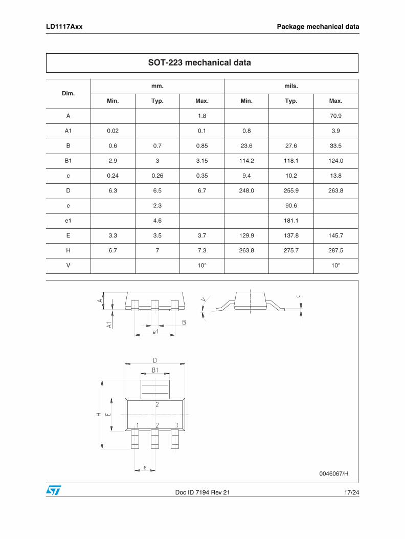
Doc ID 7194 Rev 21 17/24
Dim.mm. mils.
Min. Typ. Max. Min. Typ. Max.
A 1.8 70.9
A1 0.02 0.1 0.8 3.9
B 0.6 0.7 0.85 23.6 27.6 33.5
B1 2.9 3 3.15 114.2 118.1 124.0
c 0.24 0.26 0.35 9.4 10.2 13.8
D 6.3 6.5 6.7 248.0 255.9 263.8
e 2.3 90.6
e1 4.6 181.1
E 3.3 3.5 3.7 129.9 137.8 145.7
H 6.7 7 7.3 263.8 275.7 287.5
V 10° 10°
SOT-223 mechanical data
0046067/H
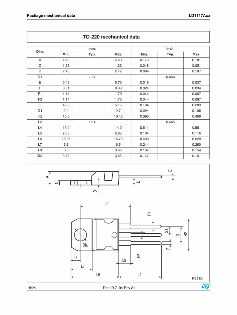
Package mechanical data LD1117Axx
18/24 Doc ID 7194 Rev 21
Dim.mm. inch.
Min. Typ. Max. Min. Typ. Max.
A 4.40 4.60 0.173 0.181
C 1.23 1.32 0.048 0.051
D 2.40 2.72 0.094 0.107
D1 1.27 0.050
E 0.49 0.70 0.019 0.027
F 0.61 0.88 0.024 0.034
F1 1.14 1.70 0.044 0.067
F2 1.14 1.70 0.044 0.067
G 4.95 5.15 0.194 0.203
G1 2.4 2.7 0.094 0.106
H2 10.0 10.40 0.393 0.409
L2 16.4 0.645
L4 13.0 14.0 0.511 0.551
L5 2.65 2.95 0.104 0.116
L6 15.25 15.75 0.600 0.620
L7 6.2 6.6 0.244 0.260
L9 3.5 3.93 0.137 0.154
DIA. 3.75 3.85 0.147 0.151
TO-220 mechanical data
P011C
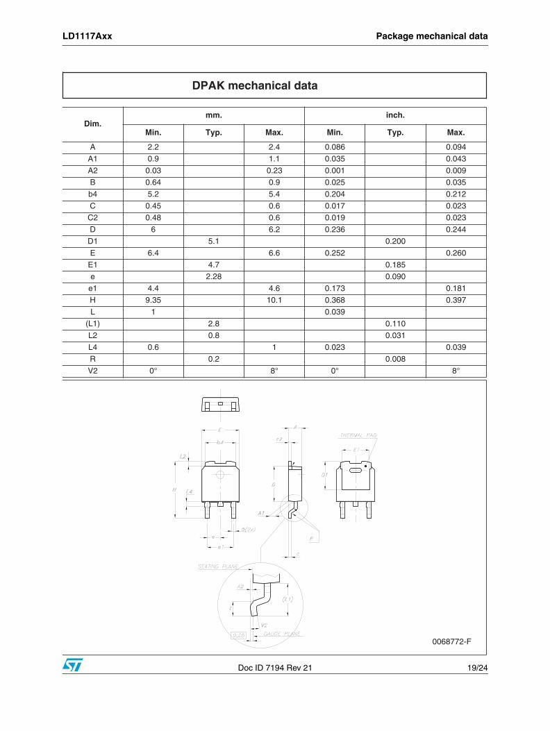
LD1117Axx Package mechanical data
Doc ID 7194 Rev 21 19/24
Dim.mm. inch.
Min. Typ. Max. Min. Typ. Max.
A 2.2 2.4 0.086 0.094
A1 0.9 1.1 0.035 0.043
A2 0.03 0.23 0.001 0.009
B 0.64 0.9 0.025 0.035
b4 5.2 5.4 0.204 0.212
C 0.45 0.6 0.017 0.023
C2 0.48 0.6 0.019 0.023
D 6 6.2 0.236 0.244
D1 5.1 0.200
E 6.4 6.6 0.252 0.260
E1 4.7 0.185
e 2.28 0.090
e1 4.4 4.6 0.173 0.181
H 9.35 10.1 0.368 0.397
L 1 0.039
(L1) 2.8 0.110
L2 0.8 0.031
L4 0.6 1 0.023 0.039
R 0.2 0.008
V2 0° 8° 0° 8°
DPAK mechanical data
0068772-F
Package mechanical data LD1117Axx
20/24 Doc ID 7194 Rev 21
Dim.mm. inch.
Min. Typ. Max. Min. Typ. Max.
A 330 12.992
C 12.8 13.0 13.2 0.504 0.512 0.519
D 20.2 0.795
N 60 2.362
T 14.4 0.567
Ao 6.73 6.83 6.93 0.265 0.269 0.273
Bo 7.32 7.42 7.52 0.288 0.292 0.296
Ko 1.78 2 0.070 0.078
Po 3.9 4.0 4.1 0.153 0.157 0.161
P 7.9 8.0 8.1 0.311 0.315 0.319
Tape & reel SOT223 mechanical data
LD1117Axx Package mechanical data
Doc ID 7194 Rev 21 21/24
Dim.mm. inch.
Min. Typ. Max. Min. Typ. Max.
A 330 12.992
C 12.8 13.0 13.2 0.504 0.512 0.519
D 20.2 0.795
N 60 2.362
T 22.4 0.882
Ao 6.80 6.90 7.00 0.268 0.272 0.2.76
Bo 10.40 10.50 10.60 0.409 0.413 0.417
Ko 2.55 2.65 2.75 0.100 0.104 0.105
Po 3.9 4.0 4.1 0.153 0.157 0.161
P 7.9 8.0 8.1 0.311 0.315 0.319
Tape & reel DPAK-PPAK mechanical data
Order codes LD1117Axx
22/24 Doc ID 7194 Rev 21
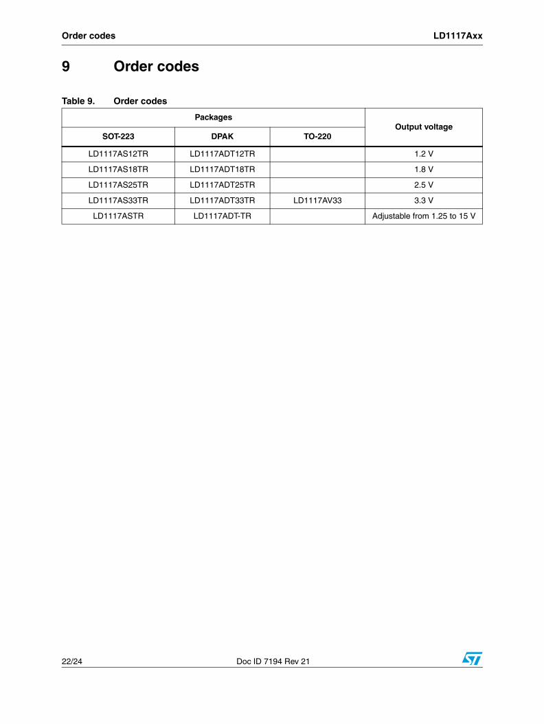
9 Order codes
Table 9. Order codes
PackagesOutput voltage
SOT-223 DPAK TO-220
LD1117AS12TR LD1117ADT12TR 1.2 V
LD1117AS18TR LD1117ADT18TR 1.8 V
LD1117AS25TR LD1117ADT25TR 2.5 V
LD1117AS33TR LD1117ADT33TR LD1117AV33 3.3 V
LD1117ASTR LD1117ADT-TR Adjustable from 1.25 to 15 V
LD1117Axx Revision history
Doc ID 7194 Rev 21 23/24
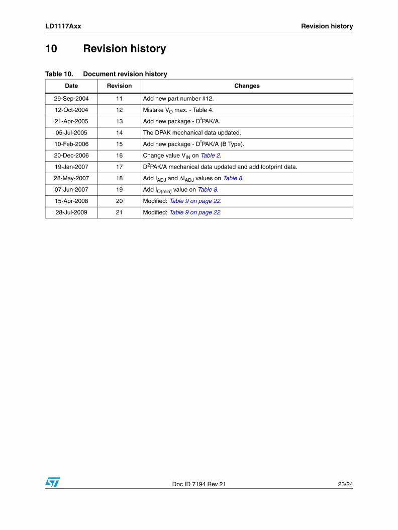
10 Revision history
Table 10. Document revision history
Date Revision Changes
29-Sep-2004 11 Add new part number #12.
12-Oct-2004 12 Mistake VO max. - Table 4.
21-Apr-2005 13 Add new package - D²PAK/A.
05-Jul-2005 14 The DPAK mechanical data updated.
10-Feb-2006 15 Add new package - D²PAK/A (B Type).
20-Dec-2006 16 Change value VIN on Table 2.
19-Jan-2007 17 D2PAK/A mechanical data updated and add footprint data.
28-May-2007 18 Add IADJ and ΔIADJ values on Table 8.
07-Jun-2007 19 Add IO(min) value on Table 8.
15-Apr-2008 20 Modified: Table 9 on page 22.
28-Jul-2009 21 Modified: Table 9 on page 22.
LD1117Axx
24/24 Doc ID 7194 Rev 21
Please Read Carefully:
Information in this document is provided solely in connection with ST products. STMicroelectronics NV and its subsidiaries (“ST”) reserve theright to make changes, corrections, modifications or improvements, to this document, and the products and services described herein at anytime, without notice.
All ST products are sold pursuant to ST’s terms and conditions of sale.
Purchasers are solely responsible for the choice, selection and use of the ST products and services described herein, and ST assumes noliability whatsoever relating to the choice, selection or use of the ST products and services described herein.
No license, express or implied, by estoppel or otherwise, to any intellectual property rights is granted under this document. If any part of thisdocument refers to any third party products or services it shall not be deemed a license grant by ST for the use of such third party productsor services, or any intellectual property contained therein or considered as a warranty covering the use in any manner whatsoever of suchthird party products or services or any intellectual property contained therein.
UNLESS OTHERWISE SET FORTH IN ST’S TERMS AND CONDITIONS OF SALE ST DISCLAIMS ANY EXPRESS OR IMPLIEDWARRANTY WITH RESPECT TO THE USE AND/OR SALE OF ST PRODUCTS INCLUDING WITHOUT LIMITATION IMPLIEDWARRANTIES OF MERCHANTABILITY, FITNESS FOR A PARTICULAR PURPOSE (AND THEIR EQUIVALENTS UNDER THE LAWSOF ANY JURISDICTION), OR INFRINGEMENT OF ANY PATENT, COPYRIGHT OR OTHER INTELLECTUAL PROPERTY RIGHT.
UNLESS EXPRESSLY APPROVED IN WRITING BY AN AUTHORIZED ST REPRESENTATIVE, ST PRODUCTS ARE NOTRECOMMENDED, AUTHORIZED OR WARRANTED FOR USE IN MILITARY, AIR CRAFT, SPACE, LIFE SAVING, OR LIFE SUSTAININGAPPLICATIONS, NOR IN PRODUCTS OR SYSTEMS WHERE FAILURE OR MALFUNCTION MAY RESULT IN PERSONAL INJURY,DEATH, OR SEVERE PROPERTY OR ENVIRONMENTAL DAMAGE. ST PRODUCTS WHICH ARE NOT SPECIFIED AS "AUTOMOTIVEGRADE" MAY ONLY BE USED IN AUTOMOTIVE APPLICATIONS AT USER’S OWN RISK.
Resale of ST products with provisions different from the statements and/or technical features set forth in this document shall immediately voidany warranty granted by ST for the ST product or service described herein and shall not create or extend in any manner whatsoever, anyliability of ST.
ST and the ST logo are trademarks or registered trademarks of ST in various countries.
Information in this document supersedes and replaces all information previously supplied.
The ST logo is a registered trademark of STMicroelectronics. All other names are the property of their respective owners.
© 2009 STMicroelectronics - All rights reserved
STMicroelectronics group of companies
Australia - Belgium - Brazil - Canada - China - Czech Republic - Finland - France - Germany - Hong Kong - India - Israel - Italy - Japan - Malaysia - Malta - Morocco - Philippines - Singapore - Spain - Sweden - Switzerland - United Kingdom - United States of America
www.st.com