Embed Size (px)
Citation preview
Low Dropout Linear Voltage Regulator
TLS715B0
TLS715B0V50
Linear Voltage Regulator
Automotive Power
Data SheetRev. 1.0, 2015-04-02
TLS715B0
Data Sheet 2 Rev. 1.0 2015-04-02
1 Overview . . . . . . . . . . . . . . . . . . . . . . . . . . . . . . . . . . . . . . . . . . . . . . . . . . . . . . . . . . . . . . . . . . . . . . 3
2 Block Diagram . . . . . . . . . . . . . . . . . . . . . . . . . . . . . . . . . . . . . . . . . . . . . . . . . . . . . . . . . . . . . . . . . . 4
3 Pin Configuration . . . . . . . . . . . . . . . . . . . . . . . . . . . . . . . . . . . . . . . . . . . . . . . . . . . . . . . . . . . . . . . 53.1 Pin Assignment PG-DSO-8 EP . . . . . . . . . . . . . . . . . . . . . . . . . . . . . . . . . . . . . . . . . . . . . . . . . . . . . . . . . . . . . . 53.2 Pin Definitions and Functions PG-DSO-8 EP . . . . . . . . . . . . . . . . . . . . . . . . . . . . . . . . . . . . . . . . . . . . . . . . . 5
4 General Product Characteristics . . . . . . . . . . . . . . . . . . . . . . . . . . . . . . . . . . . . . . . . . . . . . . . . . . . 64.1 Absolute Maximum Ratings . . . . . . . . . . . . . . . . . . . . . . . . . . . . . . . . . . . . . . . . . . . . . . . . . . . . . . . . . . . . . . . . 64.2 Functional Range . . . . . . . . . . . . . . . . . . . . . . . . . . . . . . . . . . . . . . . . . . . . . . . . . . . . . . . . . . . . . . . . . . . . . . . . . 74.3 Thermal Resistance . . . . . . . . . . . . . . . . . . . . . . . . . . . . . . . . . . . . . . . . . . . . . . . . . . . . . . . . . . . . . . . . . . . . . . . 8
5 Block Description and Electrical Characteristics . . . . . . . . . . . . . . . . . . . . . . . . . . . . . . . . . . . . . 95.1 Voltage Regulation . . . . . . . . . . . . . . . . . . . . . . . . . . . . . . . . . . . . . . . . . . . . . . . . . . . . . . . . . . . . . . . . . . . . . . . 95.2 Typical Performance Characteristics Voltage Regulator . . . . . . . . . . . . . . . . . . . . . . . . . . . . . . . . . . . . . 115.3 Current Consumption . . . . . . . . . . . . . . . . . . . . . . . . . . . . . . . . . . . . . . . . . . . . . . . . . . . . . . . . . . . . . . . . . . . . 135.4 Typical Performance Characteristics Current Consumption . . . . . . . . . . . . . . . . . . . . . . . . . . . . . . . . . . 145.5 Enable . . . . . . . . . . . . . . . . . . . . . . . . . . . . . . . . . . . . . . . . . . . . . . . . . . . . . . . . . . . . . . . . . . . . . . . . . . . . . . . . . . 155.6 Typical Performance Characteristics Enable . . . . . . . . . . . . . . . . . . . . . . . . . . . . . . . . . . . . . . . . . . . . . . . . 16
6 Application Information . . . . . . . . . . . . . . . . . . . . . . . . . . . . . . . . . . . . . . . . . . . . . . . . . . . . . . . . 176.1 Application Diagram . . . . . . . . . . . . . . . . . . . . . . . . . . . . . . . . . . . . . . . . . . . . . . . . . . . . . . . . . . . . . . . . . . . . . 176.2 Selection of External Components . . . . . . . . . . . . . . . . . . . . . . . . . . . . . . . . . . . . . . . . . . . . . . . . . . . . . . . . 176.2.1 Input Pin . . . . . . . . . . . . . . . . . . . . . . . . . . . . . . . . . . . . . . . . . . . . . . . . . . . . . . . . . . . . . . . . . . . . . . . . . . . . . . 176.2.2 Output Pin . . . . . . . . . . . . . . . . . . . . . . . . . . . . . . . . . . . . . . . . . . . . . . . . . . . . . . . . . . . . . . . . . . . . . . . . . . . . 176.3 Thermal Considerations . . . . . . . . . . . . . . . . . . . . . . . . . . . . . . . . . . . . . . . . . . . . . . . . . . . . . . . . . . . . . . . . . . 186.4 Reverse Polarity Protection . . . . . . . . . . . . . . . . . . . . . . . . . . . . . . . . . . . . . . . . . . . . . . . . . . . . . . . . . . . . . . . 196.5 Further Application Information . . . . . . . . . . . . . . . . . . . . . . . . . . . . . . . . . . . . . . . . . . . . . . . . . . . . . . . . . . 19
7 Package Outlines . . . . . . . . . . . . . . . . . . . . . . . . . . . . . . . . . . . . . . . . . . . . . . . . . . . . . . . . . . . . . . 20
8 Revision History . . . . . . . . . . . . . . . . . . . . . . . . . . . . . . . . . . . . . . . . . . . . . . . . . . . . . . . . . . . . . . . 21
Table of Contents
PG-DSO-8 EP
Type Package MarkingTLS715B0EJV50 PG-DSO-8 EP 715B0V50Data Sheet 3 Rev. 1.0, 2015-04-02
TLS715B0V50 TLS715B0
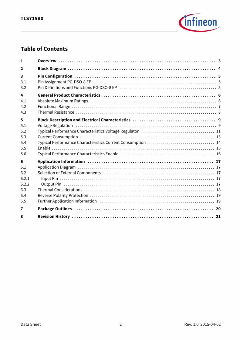
1 Overview
Features• Wide Input Voltage Range from 4.0 V to 40 V• Output Voltage 5 V• Output Voltage Precision ±2 %• Output Current up to 150 mA• Low Current Consumption of 36 µA• Very Low Dropout Voltage of typ. 200 mV at 100 mA Output Current• Stable with Small Output Capacitor of 1 µF• Enable• Overtemperature Shutdown• Output Current Limitation• Wide Temperature Range from -40 °C up to 150 °C• Green Product (RoHS compliant)• AEC Qualified
DescriptionThe TLS715B0 is a low dropout linear voltage regulator for load current up to 150 mA. An input voltage of upto 40 V is regulated to VQ,nom = 5 V with ±2 % precision. The TLS715B0, with a typical quiescent current of 36 µA, is the ideal solution for systems requiring very lowoperating current, such as those permanently connected to the battery.It features a very low dropout voltage of 200 mV, when the output current is less than 100 mA. In addition, thedropout region begins at input voltages of 4.0 V (extended operating range). This makes the TLS715B0 suitableto supply automotive systems with start-stop requirements.The device can be switched on and off by the Enable feature as described on Chapter “Enable” on Page 15.In addition, the TLS715B0’s new fast regulation concept requires only a single 1 µF output capacitor tomaintain stable regulation. The device is designed for the harsh environment of automotive applications. Therefore standard features likeoutput current limitation and overtemperature shutdown are implemented and protect the device againstfailures like output short circuit to GND, over-current and over-temperature. The TLS715B0 can be also usedin all other applications requiring a stabilized 5 V supply voltage.
Data Sheet 4 Rev. 1.0 2015-04-02
TLS715B0
Block Diagram
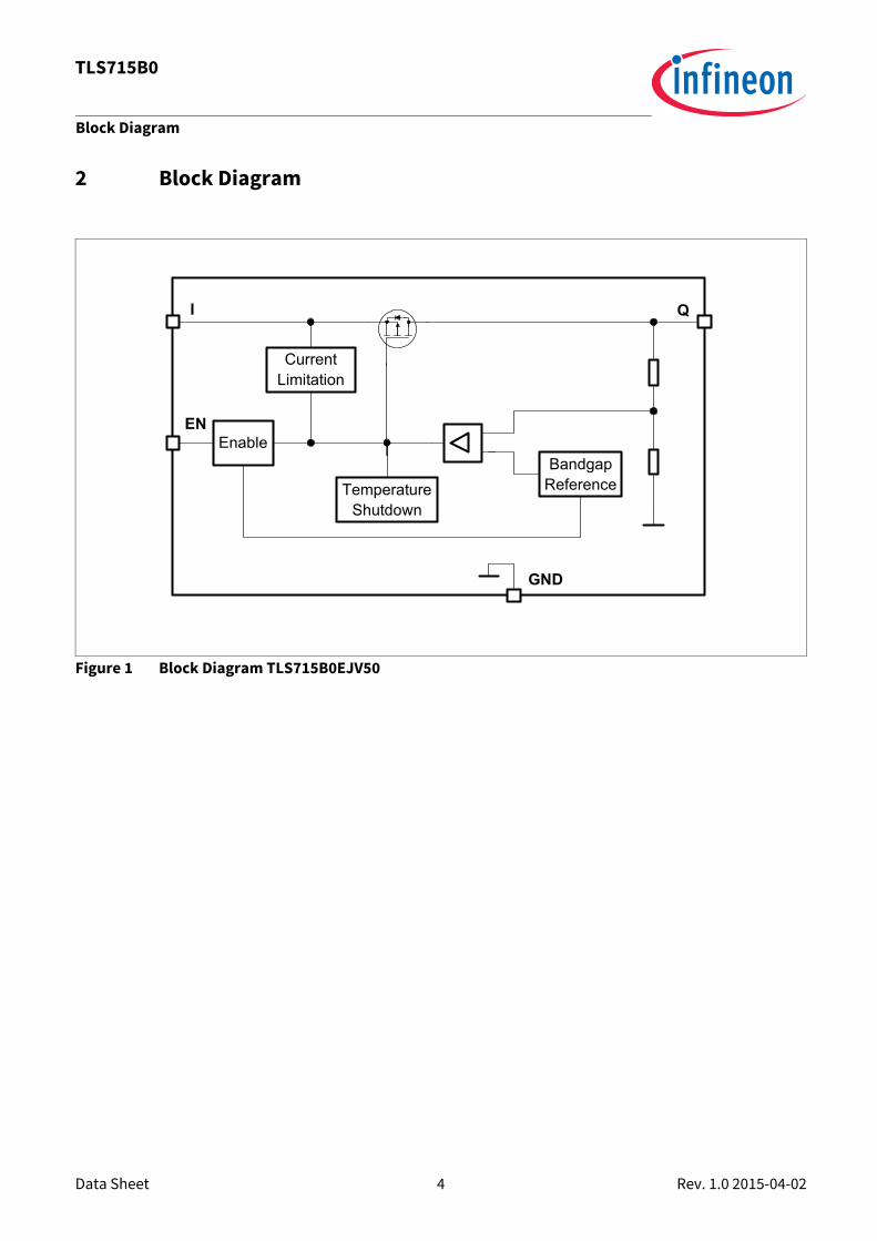
2 Block Diagram
Figure 1 Block Diagram TLS715B0EJV50
Bandgap Reference
GND
QI
Current Limitation
Temperature Shutdown
EnableEN
Data Sheet 5 Rev. 1.0 2015-04-02
TLS715B0
Pin Configuration
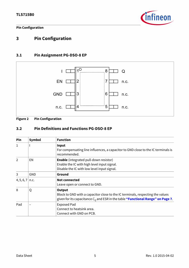
3 Pin Configuration
3.1 Pin Assignment PG-DSO-8 EP
Figure 2 Pin Configuration
3.2 Pin Definitions and Functions PG-DSO-8 EP
Pin Symbol Function1 I Input
For compensating line influences, a capacitor to GND close to the IC terminals is recommended.
2 EN Enable (integrated pull-down resistor)Enable the IC with high level input signal.Disable the IC with low level input signal.
3 GND Ground4, 5, 6, 7 n.c. Not connected
Leave open or connect to GND.
8 Q OutputBlock to GND with a capacitor close to the IC terminals, respecting the values given for its capacitance CQ and ESR in the table “Functional Range” on Page 7.
Pad – Exposed PadConnect to heatsink area.Connect with GND on PCB.
Q
n.c.
n.c.
I
EN
GND
n.c. n.c.
1
3
2
8
7
6
4 5

Data Sheet 6 Rev. 1.0 2015-04-02
TLS715B0
General Product Characteristics
4 General Product Characteristics
4.1 Absolute Maximum Ratings
Notes1. Stresses above the ones listed here may cause permanent damage to the device. Exposure to absolute
maximum rating conditions for extended periods may affect device reliability.2. Integrated protection functions are designed to prevent IC destruction under fault conditions described in the
data sheet. Fault conditions are considered as “outside” normal operating range. Protection functions are not designed for continuous repetitive operation.
Table 1 Absolute Maximum Ratings1)
Tj = -40 °C to +150 °C; all voltages with respect to ground (unless otherwise specified)
1) Not subject to production test, specified by design.
Parameter Symbol Values Unit Note or Test Condition
NumberMin. Typ. Max.
Input I, Enable ENVoltage VI, VEN -0.3 – 45 V – P_4.1.1
Output QVoltage VQ -0.3 – 7 V – P_4.1.2
TemperatureJunction Temperature Tj -40 – 150 °C – P_4.1.3
Storage Temperature Tstg -55 – 150 °C – P_4.1.4
ESD AbsorptionESD Susceptibility to GND VESD -2 – 2 kV HBM2)
2) ESD susceptibility, HBM according to ANSI/ESDA/JEDEC JS001 (1.5 kΩ, 100 pF)
P_4.1.5
ESD Susceptibility to GND VESD -750 – 750 V CDM3)
3) ESD susceptibility, Charged Device Model “CDM” according JEDEC JESD22-C101
P_4.1.6
Data Sheet 7 Rev. 1.0 2015-04-02
TLS715B0
General Product Characteristics
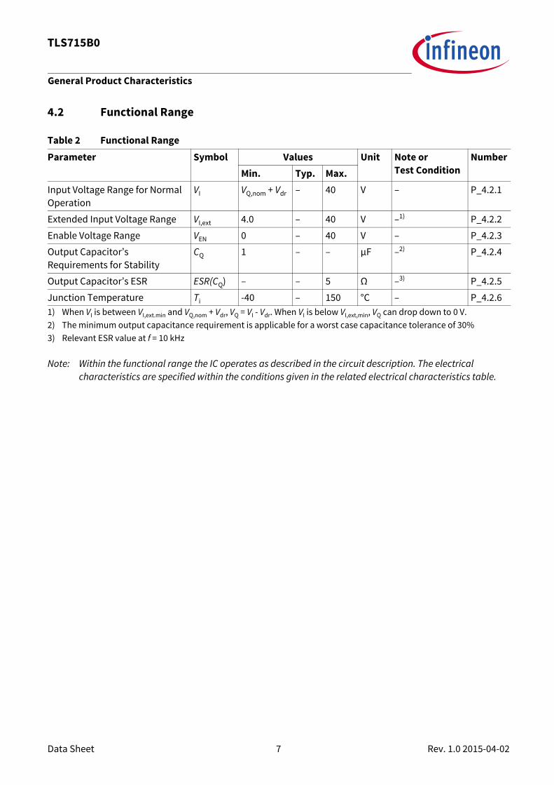
4.2 Functional Range
Note: Within the functional range the IC operates as described in the circuit description. The electrical characteristics are specified within the conditions given in the related electrical characteristics table.
Table 2 Functional RangeParameter Symbol Values Unit Note or
Test ConditionNumber
Min. Typ. Max.Input Voltage Range for Normal Operation
VI VQ,nom + Vdr – 40 V – P_4.2.1
Extended Input Voltage Range VI,ext 4.0 – 40 V –1)
1) When VI is between VI,ext.min and VQ,nom + Vdr, VQ = VI - Vdr. When VI is below VI,ext,min, VQ can drop down to 0 V.
P_4.2.2
Enable Voltage Range VEN 0 – 40 V – P_4.2.3
Output Capacitor’s Requirements for Stability
CQ 1 – – µF –2)
2) The minimum output capacitance requirement is applicable for a worst case capacitance tolerance of 30%
P_4.2.4
Output Capacitor’s ESR ESR(CQ) – – 5 Ω –3)
3) Relevant ESR value at f = 10 kHz
P_4.2.5
Junction Temperature Ti -40 – 150 °C – P_4.2.6

Data Sheet 8 Rev. 1.0 2015-04-02
TLS715B0
General Product Characteristics
4.3 Thermal Resistance
Note: This thermal data was generated in accordance with JEDEC JESD51 standards. For more information, go to www.jedec.org.
Table 3 Thermal ResistanceParameter Symbol Values Unit Note or
Test ConditionNumber
Min. Typ. Max.Package Version PG-DSO-8 EPJunction to Case1)
1) Not subject to production test, specified by design
RthJC – 13 – K/W – P_4.3.1
Junction to Ambient RthJA – 46 – K/W 2s2p board2)
2) Specified RthJA value is according to Jedec JESD51-2,-5,-7 at natural convection on FR4 2s2p board; The Product (Chip+Package) was simulated on a 76.2 x 114.3 x 1.5 mm³ board with 2 inner copper layers (2 x 70µm Cu, 2 x 35µm Cu). Where applicable a thermal via array under the exposed pad contacted the first inner copper layer.
P_4.3.2
Junction to Ambient RthJA – 153 – K/W 1s0p board, footprint only3)
3) Specified RthJA value is according to JEDEC JESD 51-3 at natural convection on FR4 1s0p board; The Product (Chip+Package) was simulated on a 76.2 × 114.3 × 1.5 mm3 board with 1 copper layer (1 x 70µm Cu).
P_4.3.3
Junction to Ambient RthJA – 71 – K/W 1s0p board, 300 mm2 heatsink area on PCB3)
P_4.3.4
Junction to Ambient RthJA – 59 – K/W 1s0p board, 600 mm2 heatsink area on PCB3)
P_4.3.5

Data Sheet 9 Rev. 1.0 2015-04-02
TLS715B0
Block Description and Electrical Characteristics
5 Block Description and Electrical Characteristics
5.1 Voltage RegulationThe output voltage VQ is divided by a resistor network. This fractional voltage is compared to an internalvoltage reference and drives the pass transistor accordingly. The control loop stability depends on the output capacitor CQ, the load current, the chip temperature and theinternal circuit design. To ensure stable operation, the output capacitor’s capacitance and its equivalentseries resistor ESR requirements given in Table 2 “Functional Range” on Page 7 must be maintained. Fordetails see the typical performance graph “Output Capacitor Series Resistor ESR(CQ) versus OutputCurrent IQ” on Page 12. Since the output capacitor is used to buffer load steps, it should be sized accordingto the application’s needs. An input capacitor CI is not required for stability, but is recommended to compensate line fluctuations. Anadditional reverse polarity protection diode and a combination of several capacitors for filtering should beused, in case the input is connected directly to the battery line. Connect the capacitors close to the regulatorterminals.Whenever the load current exceeds the specified limit, e.g. in case of a short circuit, the output current islimited and the output voltage decreases.The overtemperature shutdown circuit prevents the IC from immediate destruction under fault conditions(e.g. output continuously short-circuited) by switching off the power stage. After the chip has cooled, theregulator restarts. This oscillatory thermal behaviour causes the junction temperature to exceed themaximum rating of 150°C and can significantly reduce the IC’s lifetime.
Figure 3 Block Diagram Voltage Regulation
LOAD
Supply
CI
Regulated Output VoltageIQII
VI VQ
C
ESRCQ
Bandgap Reference
GND
QI
Current Limitation
Temperature Shutdown
EnableEN
Data Sheet 10 Rev. 1.0 2015-04-02
TLS715B0
Block Description and Electrical Characteristics
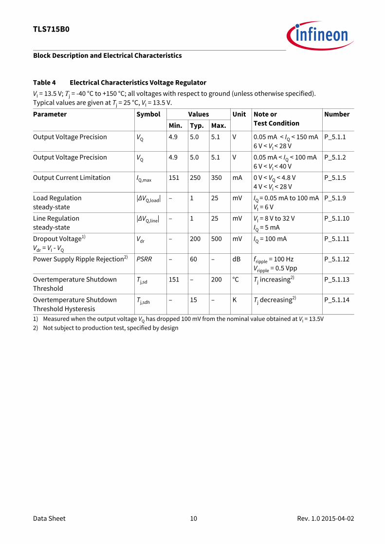
Table 4 Electrical Characteristics Voltage RegulatorVI = 13.5 V; Tj = -40 °C to +150 °C; all voltages with respect to ground (unless otherwise specified).Typical values are given at Tj = 25 °C, VI = 13.5 V.
Parameter Symbol Values Unit Note or Test Condition
NumberMin. Typ. Max.
Output Voltage Precision VQ 4.9 5.0 5.1 V 0.05 mA < IQ < 150 mA6 V < VI < 28 V
P_5.1.1
Output Voltage Precision VQ 4.9 5.0 5.1 V 0.05 mA < IQ < 100 mA6 V < VI < 40 V
P_5.1.2
Output Current Limitation IQ,max 151 250 350 mA 0 V < VQ < 4.8 V4 V < VI < 28 V
P_5.1.5
Load Regulationsteady-state
|∆VQ,load| – 1 25 mV IQ = 0.05 mA to 100 mAVI = 6 V
P_5.1.9
Line Regulationsteady-state
|∆VQ,line| – 1 25 mV VI = 8 V to 32 VIQ = 5 mA
P_5.1.10
Dropout Voltage1)
Vdr = VI - VQ
1) Measured when the output voltage VQ has dropped 100 mV from the nominal value obtained at VI = 13.5V
Vdr – 200 500 mV IQ = 100 mA P_5.1.11
Power Supply Ripple Rejection2)
2) Not subject to production test, specified by design
PSRR – 60 – dB fripple = 100 HzVripple = 0.5 Vpp
P_5.1.12
Overtemperature Shutdown Threshold
Tj,sd 151 – 200 °C Tj increasing2) P_5.1.13
Overtemperature Shutdown Threshold Hysteresis
Tj,sdh – 15 – K Tj decreasing2) P_5.1.14
Data Sheet 11 Rev. 1.0 2015-04-02
TLS715B0
Block Description and Electrical Characteristics
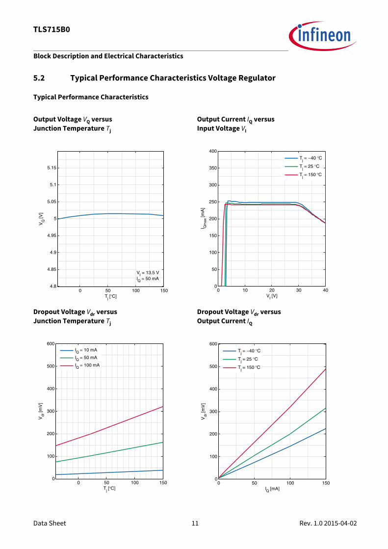
5.2 Typical Performance Characteristics Voltage Regulator
Typical Performance Characteristics
Output Voltage VQ versusJunction Temperature Tj
Output Current IQ versusInput Voltage VI
Dropout Voltage Vdr versusJunction Temperature Tj
Dropout Voltage Vdr versusOutput Current IQ
0 50 100 1504.8
4.85
4.9
4.95
5
5.05
5.1
5.15
Tj [°C]
VQ
[V]
VI = 13.5 VIQ = 50 mA
0 10 20 30 400
50
100
150
200
250
300
350
400
VI [V]
I Qm
ax [m
A]
Tj = −40 °C
Tj = 25 °C
Tj = 150 °C
0 50 100 1500
100
200
300
400
500
600
Tj [°C]
Vdr
[mV
]
IQ = 10 mA
IQ = 50 mA
IQ = 100 mA
0 50 100 1500
100
200
300
400
500
600
IQ [mA]
Vdr
[mV
]
Tj = −40 °C
Tj = 25 °C
Tj = 150 °C
Data Sheet 12 Rev. 1.0 2015-04-02
TLS715B0
Block Description and Electrical Characteristics
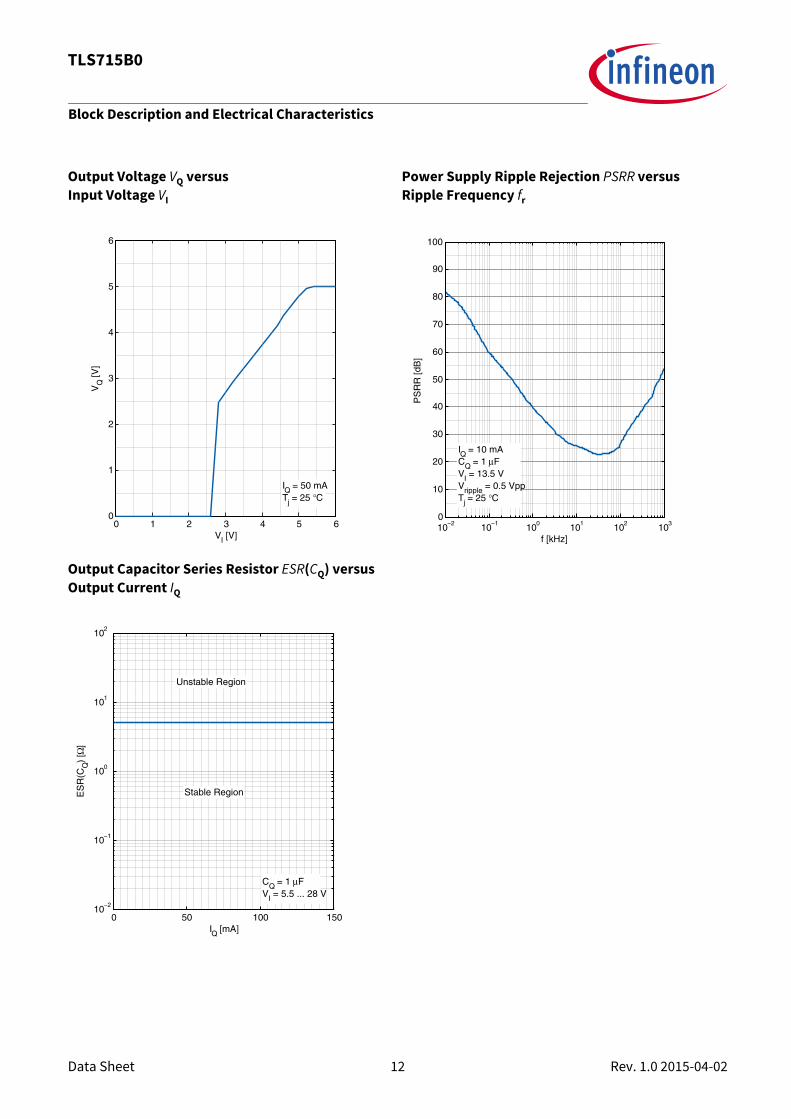
Output Voltage VQ versusInput Voltage VI
Power Supply Ripple Rejection PSRR versusRipple Frequency fr
Output Capacitor Series Resistor ESR(CQ) versusOutput Current IQ
0 1 2 3 4 5 60
1
2
3
4
5
6
VI [V]
VQ
[V]
IQ = 50 mATj = 25 °C
10−2 10−1 100 101 102 1030
10
20
30
40
50
60
70
80
90
100
f [kHz]
PS
RR
[dB
]
IQ = 10 mACQ = 1 μFVI = 13.5 VVripple = 0.5 VppTj = 25 °C
0 50 100 15010−2
10−1
100
101
102
IQ [mA]
ES
R(C
Q)
[Ω]
CQ = 1 μFVI = 5.5 ... 28 V
Stable Region
Unstable Region
Data Sheet 13 Rev. 1.0 2015-04-02
TLS715B0
Block Description and Electrical Characteristics
5.3 Current Consumption
Table 5 Electrical Characteristics Current ConsumptionVI = 13.5 V; Tj = -40 °C to +150 °C (unless otherwise specified).Typical values are given at Tj = 25 °C, VI = 13.5 V.
Parameter Symbol Values Unit Note or Test Condition
NumberMin. Typ. Max.
Current ConsumptionIq = II
Iq,off – 1.5 5 µA VEN ≤ 0.4 VTj < 105 °C
P_5.3.1
Current ConsumptionIq = II - IQ
Iq – 36 80 µA 0.05 mA < IQ < 100 mA P_5.3.2
Data Sheet 14 Rev. 1.0 2015-04-02
TLS715B0
Block Description and Electrical Characteristics
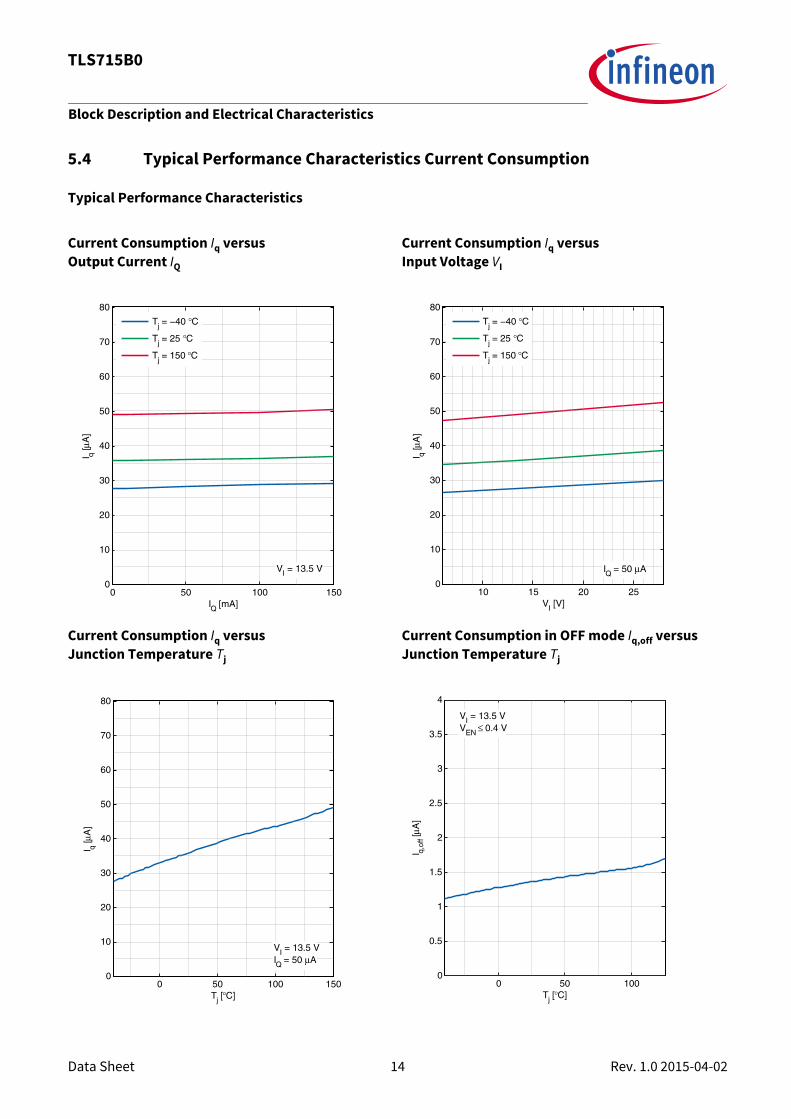
5.4 Typical Performance Characteristics Current Consumption
Typical Performance Characteristics
Current Consumption Iq versusOutput Current IQ
Current Consumption Iq versusInput Voltage VI
Current Consumption Iq versusJunction Temperature Tj
Current Consumption in OFF mode Iq,off versusJunction Temperature Tj
0 50 100 1500
10
20
30
40
50
60
70
80
IQ [mA]
I q [μA
]
VI = 13.5 V
Tj = −40 °C
Tj = 25 °C
Tj = 150 °C
10 15 20 250
10
20
30
40
50
60
70
80
VI [V]
I q [μA
]
IQ = 50 μA
Tj = −40 °C
Tj = 25 °C
Tj = 150 °C
0 50 100 1500
10
20
30
40
50
60
70
80
Tj [°C]
I q [μA
]
VI = 13.5 VIQ = 50 μA
0 50 1000
0.5
1
1.5
2
2.5
3
3.5
4
Tj [°C]
I q,of
f [μA
]
VI = 13.5 VVEN ≤ 0.4 V
Data Sheet 15 Rev. 1.0 2015-04-02
TLS715B0
Block Description and Electrical Characteristics
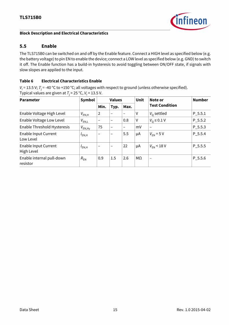
5.5 EnableThe TLS715B0 can be switched on and off by the Enable feature. Connect a HIGH level as specified below (e.g.the battery voltage) to pin EN to enable the device; connect a LOW level as specified below (e.g. GND) to switchit off. The Enable function has a build-in hysteresis to avoid toggling between ON/OFF state, if signals withslow slopes are appiled to the input.
Table 6 Electrical Characteristics EnableVI = 13.5 V; Tj = -40 °C to +150 °C; all voltages with respect to ground (unless otherwise specified).Typical values are given at Tj = 25 °C, VI = 13.5 V.
Parameter Symbol Values Unit Note or Test Condition
NumberMin. Typ. Max.
Enable Voltage High Level VEN,H 2 – – V VQ settled P_5.5.1
Enable Voltage Low Level VEN,L – – 0.8 V VQ ≤ 0.1 V P_5.5.2
Enable Threshold Hysteresis VEN,Hy 75 – – mV – P_5.5.3
Enable Input CurrentLow Level
IEN,H – – 5.5 µA VEN = 5 V P_5.5.4
Enable Input CurrentHigh Level
IEN,H – – 22 µA VEN < 18 V P_5.5.5
Enable internal pull-down resistor
REN 0.9 1.5 2.6 MΩ – P_5.5.6

Data Sheet 16 Rev. 1.0 2015-04-02
TLS715B0
Block Description and Electrical Characteristics
5.6 Typical Performance Characteristics Enable
Typical Performance Characteristics
Enabled Input Current IEN versusEnabled Input Voltage VEN
0 10 20 30 400
5
10
15
20
25
30
35
40
VEN [V]
I EN [μ
A]
Tj = −40 °C
Tj = 25 °C
Tj = 150 °C
Data Sheet 17 Rev. 1.0 2015-04-02
TLS715B0
Application Information
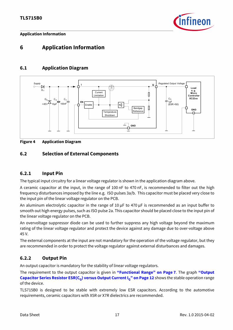
6 Application Information
6.1 Application Diagram
Figure 4 Application Diagram
6.2 Selection of External Components
6.2.1 Input PinThe typical input circuitry for a linear voltage regulator is shown in the application diagram above.A ceramic capacitor at the input, in the range of 100 nF to 470 nF, is recommended to filter out the highfrequency disturbances imposed by the line e.g. ISO pulses 3a/b. This capacitor must be placed very close tothe input pin of the linear voltage regulator on the PCB. An aluminum electrolytic capacitor in the range of 10 µF to 470 µF is recommended as an input buffer tosmooth out high energy pulses, such as ISO pulse 2a. This capacitor should be placed close to the input pin ofthe linear voltage regulator on the PCB.An overvoltage suppressor diode can be used to further suppress any high voltage beyond the maximumrating of the linear voltage regulator and protect the device against any damage due to over-voltage above45 V.The external components at the input are not mandatory for the operation of the voltage regulator, but theyare recommended in order to protect the voltage regulator against external disturbances and damages.
6.2.2 Output PinAn output capacitor is mandatory for the stability of linear voltage regulators. The requirement to the output capacitor is given in “Functional Range” on Page 7. The graph “OutputCapacitor Series Resistor ESR(CQ) versus Output Current IQ” on Page 12 shows the stable operation rangeof the device.TLS715B0 is designed to be stable with extremely low ESR capacitors. According to the automotiverequirements, ceramic capacitors with X5R or X7R dielectrics are recommended.
CQ
Loade. g.
Micro Controller
XC22xx
GND
Regulated Output VoltageSupply
100nF10µF
CI1CI2
<45V
DI21µF (ESR <5Ω)
DI1
Bandgap Reference
GND
QI
Current Limitation
Temperature Shutdown
EnableEN
Data Sheet 18 Rev. 1.0 2015-04-02
TLS715B0
Application Information
The output capacitor should be placed as close as possible to the regulator’s output and GND pins and on thesame side of the PCB as the regulator itself.In case of rapid transients of input voltage or load current, the capacitance should be dimensioned inaccordance and verified in the real application that the output stability requirements are fulfilled.
6.3 Thermal ConsiderationsKnowing the input voltage, the output voltage and the load profile of the application, the total powerdissipation can be calculated:
PD = (VI - VQ) × IQ + VI × Iq (6.1)
with• PD: continuous power dissipation• VI : input voltage• VQ: output voltage• IQ: output current• Iq: quiescent current
The maximum acceptable thermal resistance RthJA can then be calculated:
RthJA,max = ( Tj,max - Ta ) / PD (6.2)
with• Tj,max: maximum allowed junction temperature• Ta: ambient temperature
Based on the above calculation the proper PCB type and the necessary heat sink area can be determined withreference to the specification in “Thermal Resistance” on Page 8.ExampleApplication conditions:VI = 13.5 VVQ = 5 VIQ = 100 mATa = 85 °C
Calculation of RthJA,max:PD= (VI – VQ) × IQ + VI × Iq (VI × Iq can be neglected because of very low Iq)= (13.5 V – 5 V) × 100 mA= 0.85 WRthJA,max= (Tj,max – Ta) / PD
= (150 °C – 85 °C) / 0.85 W = 76.47 K/W

Data Sheet 19 Rev. 1.0 2015-04-02
TLS715B0
Application Information
As a result, the PCB design must ensure a thermal resistance RthJA lower than 76.47 K/W. According to“Thermal Resistance” on Page 8, at least 300 mm2 heatsink area is needed on the FR4 1s0p PCB, or the FR42s2p board can be used.
6.4 Reverse Polarity ProtectionTLS715B0 is not self protected against reverse polarity faults and must be protected by external componentsagainst negative supply voltage. An external reverse polarity diode is needed. The absolute maximum ratingsof the device as specified in “Absolute Maximum Ratings” on Page 6 must be kept.
6.5 Further Application Information• For further information you may contact http://www.infineon.com/
Data Sheet 20 Rev. 1.0 2015-04-02
TLS715B0
Package Outlines
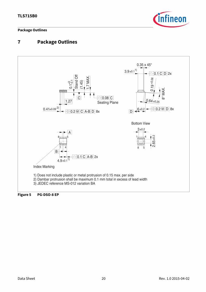
7 Package Outlines
Figure 5 PG-DSO-8 EP
1 4
8 5
8
1 4
5
8x0.41±0.09 2)
M0.2 DC A-B
1.27C
Sta
nd O
ff
+0 -0.1
0.1
(1.4
5)
1.7
MA
X.
0.08Seating Plane
C
A
B
4.9±0.11)A-BC0.1 2x
3) JEDEC reference MS-012 variation BA
1) Does not include plastic or metal protrusion of 0.15 max. per side 2) Dambar protrusion shall be maximum 0.1 mm total in excess of lead width
Bottom View
±0.23
±0.2
2.65
0.2±0.2D
6 M D 8x
0.64±0.25
3.9±0.11)0.1
0.35 x 45°
C D 2x
+0.0
60.
19
8° M
AX
.Index Marking
Data Sheet 21 Rev. 1.0 2015-04-02
TLS715B0
Revision History
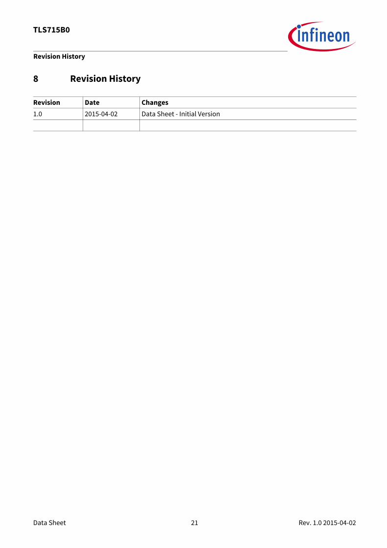
8 Revision History
Revision Date Changes1.0 2015-04-02 Data Sheet - Initial Version
Trademarks of Infineon Technologies AGAURIX™, C166™, CanPAK™, CIPOS™, CIPURSE™, CoolMOS™, CoolSET™, CORECONTROL™, CROSSAVE™, DAVE™, DI-POL™, EasyPIM™, EconoBRIDGE™,EconoDUAL™, EconoPIM™, EconoPACK™, EiceDRIVER™, eupec™, FCOS™, HITFET™, HybridPACK™, I²RF™, ISOFACE™, IsoPACK™, LITIX™, MIPAQ™,ModSTACK™, my-d™, NovalithIC™, OptiMOS™, ORIGA™, POWERCODE™, PRIMARION™, PrimePACK™, PrimeSTACK™, PRO-SIL™, PROFET™, RASIC™,ReverSave™, SatRIC™, SIEGET™, SINDRION™, SIPMOS™, SmartLEWIS™, SPOC™, SOLID FLASH™, TEMPFET™, thinQ!™, TRENCHSTOP™, TriCore™.Other TrademarksAdvance Design System™ (ADS) of Agilent Technologies, AMBA™, ARM™, MULTI-ICE™, KEIL™, PRIMECELL™, REALVIEW™, THUMB™, µVision™ of ARM Limited,UK. AUTOSAR™ is licensed by AUTOSAR development partnership. Bluetooth™ of Bluetooth SIG Inc. CAT-iq™ of DECT Forum. COLOSSUS™, FirstGPS™ ofTrimble Navigation Ltd. EMV™ of EMVCo, LLC (Visa Holdings Inc.). EPCOS™ of Epcos AG. FLEXGO™ of Microsoft Corporation. FlexRay™ is licensed by FlexRayConsortium. HYPERTERMINAL™ of Hilgraeve Incorporated. IEC™ of Commission Electrotechnique Internationale. IrDA™ of Infrared Data AssociationCorporation. ISO™ of INTERNATIONAL ORGANIZATION FOR STANDARDIZATION. MATLAB™ of MathWorks, Inc. MAXIM™ of Maxim Integrated Products, Inc.MICROTEC™, NUCLEUS™ of Mentor Graphics Corporation. MIPI™ of MIPI Alliance, Inc. MIPS™ of MIPS Technologies, Inc., USA. muRata™ of MURATAMANUFACTURING CO., MICROWAVE OFFICE™ (MWO) of Applied Wave Research Inc., OmniVision™ of OmniVision Technologies, Inc. Openwave™ OpenwaveSystems Inc. RED HAT™ Red Hat, Inc. RFMD™ RF Micro Devices, Inc. SIRIUS™ of Sirius Satellite Radio Inc. SOLARIS™ of Sun Microsystems, Inc. SPANSION™ ofSpansion LLC Ltd. Symbian™ of Symbian Software Limited. TAIYO YUDEN™ of Taiyo Yuden Co. TEAKLITE™ of CEVA, Inc. TEKTRONIX™ of Tektronix Inc.TOKO™ of TOKO KABUSHIKI KAISHA TA. UNIX™ of X/Open Company Limited. VERILOG™, PALLADIUM™ of Cadence Design Systems, Inc. VLYNQ™ of TexasInstruments Incorporated. VXWORKS™, WIND RIVER™ of WIND RIVER SYSTEMS, INC. ZETEX™ of Diodes Zetex Limited.Last Trademarks Update 2011-11-11
Edition 2015-04-02Published by Infineon Technologies AG81726 Munich, Germany
© 2014 Infineon Technologies AG.All Rights Reserved.
Do you have a question about any aspect of this document?Email: [email protected]
Document referenceDoc_Number
Legal DisclaimerThe information given in this document shall inno event be regarded as a guarantee ofconditions or characteristics. With respect to anyexamples or hints given herein, any typicalvalues stated herein and/or any informationregarding the application of the device, InfineonTechnologies hereby disclaims any and allwarranties and liabilities of any kind, includingwithout limitation, warranties of non-infringement of intellectual property rights ofany third party.InformationFor further information on technology, deliveryterms and conditions and prices, please contactthe nearest Infineon Technologies Office(www.infineon.com).
WarningsDue to technical requirements, componentsmay contain dangerous substances. Forinformation on the types in question, pleasecontact the nearest Infineon TechnologiesOffice. Infineon Technologies components maybe used in life-support devices or systems onlywith the express written approval of InfineonTechnologies, if a failure of such componentscan reasonably be expected to cause the failureof that life-support device or system or to affectthe safety or effectiveness of that device orsystem. Life support devices or systems areintended to be implanted in the human body orto support and/or maintain and sustain and/orprotect human life. If they fail, it is reasonable toassume that the health of the user or otherpersons may be endangered.
www.infineon.com
Mouser Electronics
Authorized Distributor
Click to View Pricing, Inventory, Delivery & Lifecycle Information: Infineon:
TLS715B0EJV50XUMA1


![53619279 Linear Amp Switching Voltage Regulator Handbook[1]](https://img.pdfslide.net/doc/110x75/54f73ea34a7959430c8b4ee1/53619279-linear-amp-switching-voltage-regulator-handbook1.jpg)