Embed Size (px)
Citation preview
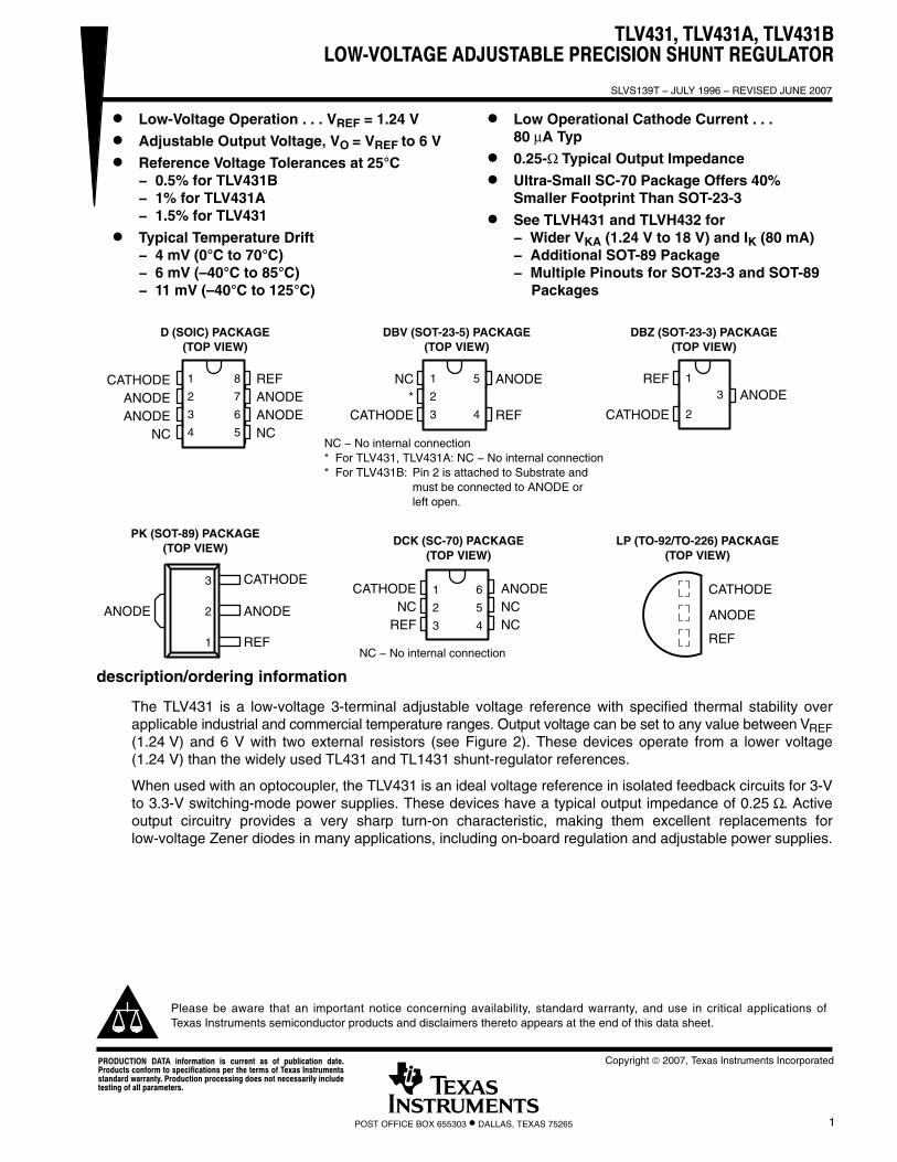
TLV431, TLV431A, TLV431BLOW-VOLTAGE ADJUSTABLE PRECISION SHUNT REGULATOR
SLVS139T − JULY 1996 − REVISED JUNE 2007
1POST OFFICE BOX 655303 • DALLAS, TEXAS 75265
Low-Voltage Operation . . . VREF = 1.24 V
Adjustable Output Voltage, VO = VREF to 6 V
Reference Voltage Tolerances at 25C− 0.5% for TLV431B− 1% for TLV431A− 1.5% for TLV431
Typical Temperature Drift− 4 mV (0C to 70C)− 6 mV (–40C to 85C)− 11 mV (–40C to 125C)
Low Operational Cathode Current . . .80 µA Typ
0.25-Ω Typical Output Impedance
Ultra-Small SC-70 Package Offers 40%Smaller Footprint Than SOT-23-3
See TLVH431 and TLVH432 for− Wider VKA (1.24 V to 18 V) and IK (80 mA)− Additional SOT-89 Package− Multiple Pinouts for SOT-23-3 and SOT-89
Packages
REF
ANODE
CATHODE
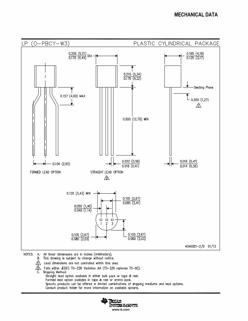
LP (TO-92/TO-226) PACKAGE(TOP VIEW)
NC − No internal connection* For TLV431, TLV431A: NC − No internal connection* For TLV431B: Pin 2 is attached to Substrate and
must be connected to ANODE or left open.
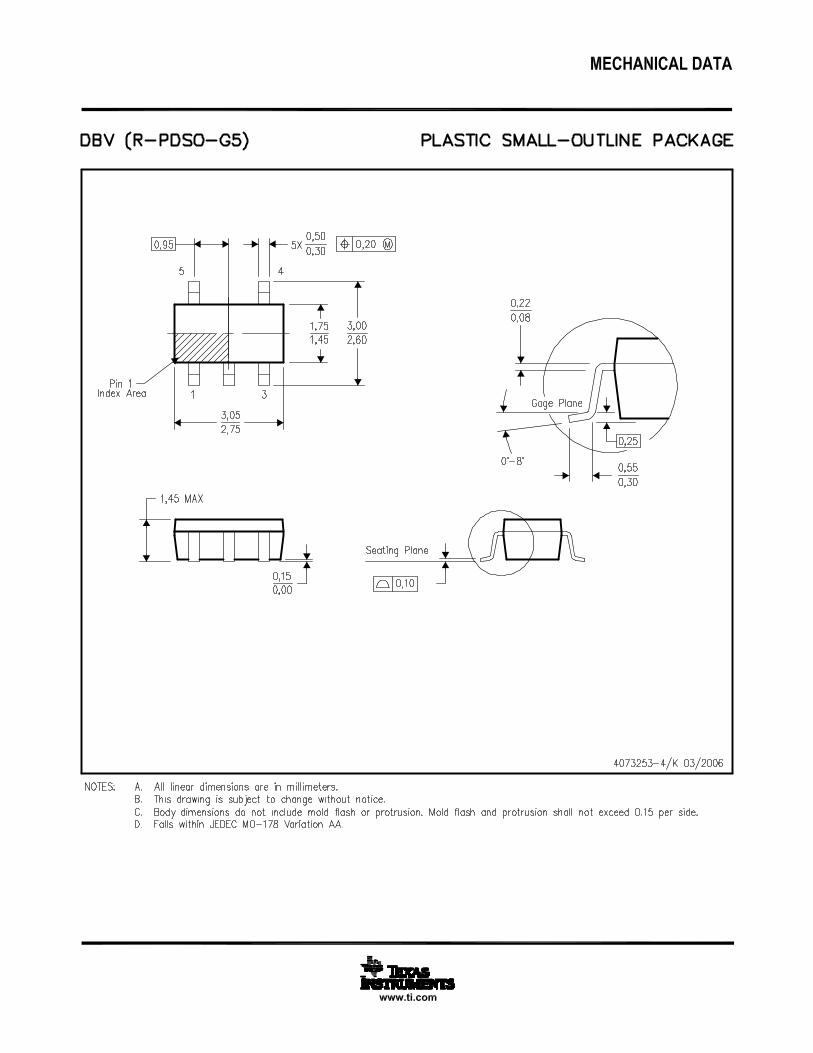
DBV (SOT-23-5) PACKAGE(TOP VIEW)
1
2
3
5
4
NC*
CATHODE
ANODE
REF
DBZ (SOT-23-3) PACKAGE(TOP VIEW)
1
2
3REF
CATHODE
ANODE
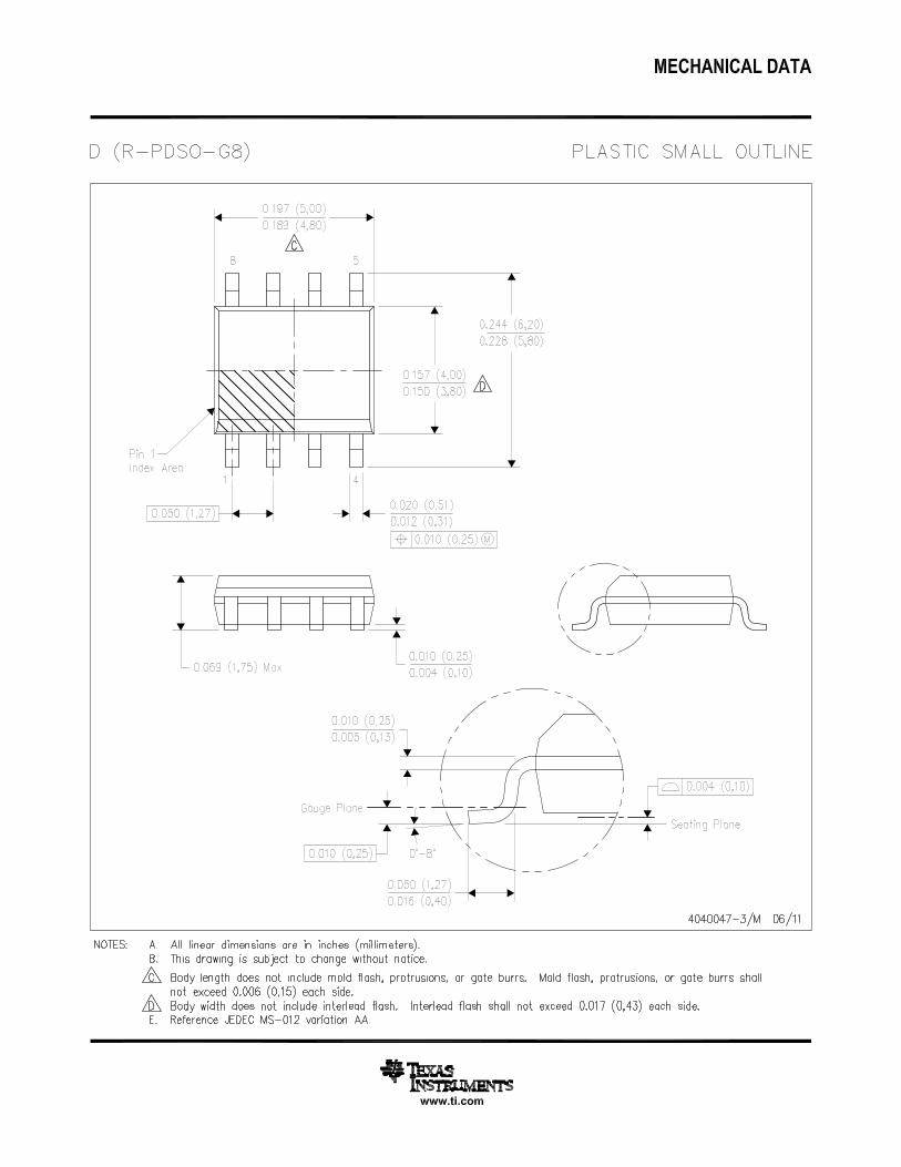
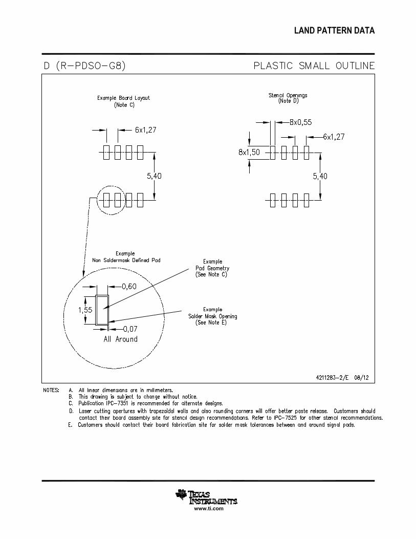
D (SOIC) PACKAGE(TOP VIEW)
1
2
3
4
8
7
6
5
REFANODEANODENC
CATHODEANODEANODE
NC
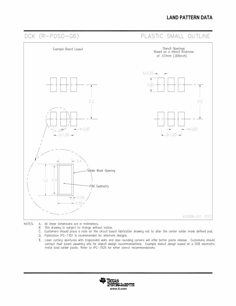
DCK (SC-70) PACKAGE(TOP VIEW)
1
2
3
6
5
4
CATHODENC
REF
ANODENCNC
NC − No internal connection
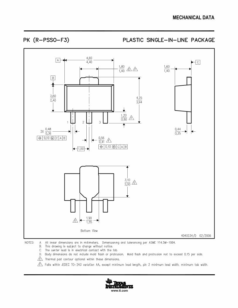
PK (SOT-89) PACKAGE(TOP VIEW)
1
3
2
REF
CATHODE
ANODEANODE
description/ordering information
The TLV431 is a low-voltage 3-terminal adjustable voltage reference with specified thermal stability overapplicable industrial and commercial temperature ranges. Output voltage can be set to any value between VREF(1.24 V) and 6 V with two external resistors (see Figure 2). These devices operate from a lower voltage(1.24 V) than the widely used TL431 and TL1431 shunt-regulator references.
When used with an optocoupler, the TLV431 is an ideal voltage reference in isolated feedback circuits for 3-Vto 3.3-V switching-mode power supplies. These devices have a typical output impedance of 0.25 Ω. Activeoutput circuitry provides a very sharp turn-on characteristic, making them excellent replacements forlow-voltage Zener diodes in many applications, including on-board regulation and adjustable power supplies.
Please be aware that an important notice concerning availability, standard warranty, and use in critical applications ofTexas Instruments semiconductor products and disclaimers thereto appears at the end of this data sheet.
Copyright 2007, Texas Instruments IncorporatedPRODUCTION DATA information is current as of publication date.Products conform to specifications per the terms of Texas Instrumentsstandard warranty. Production processing does not necessarily includetesting of all parameters.
TLV431, TLV431A, TLV431BLOW-VOLTAGE ADJUSTABLE PRECISION SHUNT REGULATOR
SLVS139T − JULY 1996 − REVISED JUNE 2007
2 POST OFFICE BOX 655303 • DALLAS, TEXAS 75265
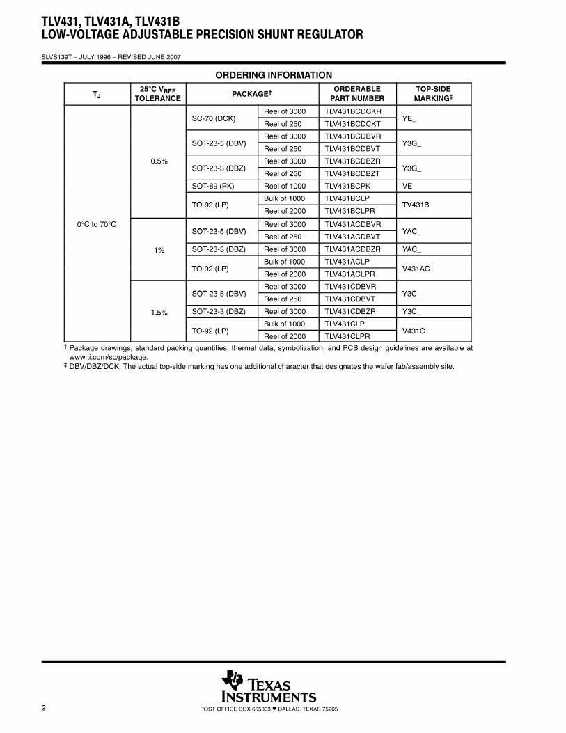
ORDERING INFORMATION
TJ25C VREF
TOLERANCE PACKAGE† ORDERABLEPART NUMBER
TOP-SIDEMARKING‡
SC 70 (DCK)Reel of 3000 TLV431BCDCKR
YESC-70 (DCK)Reel of 250 TLV431BCDCKT
YE_
SOT 23 5 (DBV)Reel of 3000 TLV431BCDBVR
Y3GSOT-23-5 (DBV)Reel of 250 TLV431BCDBVT
Y3G_
0.5%SOT 23 3 (DBZ)
Reel of 3000 TLV431BCDBZRY3GSOT-23-3 (DBZ)
Reel of 250 TLV431BCDBZTY3G_
SOT-89 (PK) Reel of 1000 TLV431BCPK VE
TO 92 (LP)Bulk of 1000 TLV431BCLP
TV431BTO-92 (LP)Reel of 2000 TLV431BCLPR
TV431B
0°C to 70°CSOT 23 5 (DBV)
Reel of 3000 TLV431ACDBVRYACSOT-23-5 (DBV)
Reel of 250 TLV431ACDBVTYAC_
1% SOT-23-3 (DBZ) Reel of 3000 TLV431ACDBZR YAC_1%
TO 92 (LP)Bulk of 1000 TLV431ACLP
V431ACTO-92 (LP)Reel of 2000 TLV431ACLPR
V431AC
SOT 23 5 (DBV)Reel of 3000 TLV431CDBVR
Y3CSOT-23-5 (DBV)Reel of 250 TLV431CDBVT
Y3C_
1.5% SOT-23-3 (DBZ) Reel of 3000 TLV431CDBZR Y3C_1.5%
TO 92 (LP)Bulk of 1000 TLV431CLP
V431CTO-92 (LP)Reel of 2000 TLV431CLPR
V431C
† Package drawings, standard packing quantities, thermal data, symbolization, and PCB design guidelines are available atwww.ti.com/sc/package.
‡ DBV/DBZ/DCK: The actual top-side marking has one additional character that designates the wafer fab/assembly site.
TLV431, TLV431A, TLV431BLOW-VOLTAGE ADJUSTABLE PRECISION SHUNT REGULATOR
SLVS139T − JULY 1996 − REVISED JUNE 2007
3POST OFFICE BOX 655303 • DALLAS, TEXAS 75265
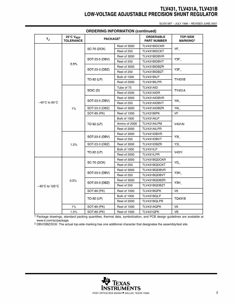
ORDERING INFORMATION (continued)
TJ25C VREF
TOLERANCE PACKAGE† ORDERABLEPART NUMBER
TOP-SIDEMARKING‡
SC 70 (DCK)Reel of 3000 TLV431BIDCKR
YFSC-70 (DCK)Reel of 250 TLV431BIDCKT
YF_
SOT 23 5 (DBV)Reel of 3000 TLV431BIDBVR
Y3F
0 5%
SOT-23-5 (DBV)Reel of 250 TLV431BIDBVT
Y3F_
0.5%
SOT 23 3 (DBZ)Reel of 3000 TLV431BIDBZR
Y3FSOT-23-3 (DBZ)Reel of 250 TLV431BIDBZT
Y3F_
TO 92 (LP)Bulk of 1000 TLV431BILP
TY431BTO-92 (LP)Reel of 2000 TLV431BILPR
TY431B
SOIC (D)Tube of 75 TLV431AID
TY431ASOIC (D)Reel of 2500 TLV431AIDR
TY431A
SOT 23 5 (DBV)Reel of 3000 TLV431AIDBVR
YAI−40°C to 85°C SOT-23-5 (DBV)Reel of 250 TLV431AIDBVT
YAI_
1% SOT-23-3 (DBZ) Reel of 3000 TLV431AIDBZR YAI_1%
SOT-89 (PK) Reel of 1000 TLV431BIPK VF
Bulk of 1000 TLV431AILP
TO-92 (LP) Ammo of 2000 TLV431AILPM V431AITO 92 (LP)
Reel of 2000 TLV431AILPR
V431AI
SOT 23 5 (DBV)Reel of 3000 TLV431IDBVR
Y3ISOT-23-5 (DBV)Reel of 250 TLV431IDBVT
Y3I_
1.5% SOT-23-3 (DBZ) Reel of 3000 TLV431IDBZR Y3I_1.5%
TO 92 (LP)Bulk of 1000 TLV431ILP
V431ITO-92 (LP)Reel of 2000 TLV431ILPR
V431I
SC 70 (DCK)Reel of 3000 TLV431BQDCKR
YGSC-70 (DCK)Reel of 250 TLV431BQDCKT
YG_
SOT 23 5 (DBV)Reel of 3000 TLV431BQDBVR
Y3HSOT-23-5 (DBV)Reel of 250 TLV431BQDBVT
Y3H_
0.5%SOT 23 3 (DBZ)
Reel of 3000 TLV431BQDBZRY3H
−40°C to 125°C
0.5%SOT-23-3 (DBZ)
Reel of 250 TLV431BQDBZTY3H_
40 C to 125 C
SOT-89 (PK) Reel of 1000 TLV431BQPK V6
TO 92 (LP)Bulk of 1000 TLV431BQLP
TQ431BTO-92 (LP)Reel of 2000 TLV431BQLPR
TQ431B
1% SOT-89 (PK) Reel of 1000 TLV431AQPK VA
1.5% SOT-89 (PK) Reel of 1000 TLV431QPK VB† Package drawings, standard packing quantities, thermal data, symbolization, and PCB design guidelines are available at
www.ti.com/sc/package.‡ DBV/DBZ/DCK: The actual top-side marking has one additional character that designates the assembly/test site.
TLV431, TLV431A, TLV431BLOW-VOLTAGE ADJUSTABLE PRECISION SHUNT REGULATOR
SLVS139T − JULY 1996 − REVISED JUNE 2007
4 POST OFFICE BOX 655303 • DALLAS, TEXAS 75265
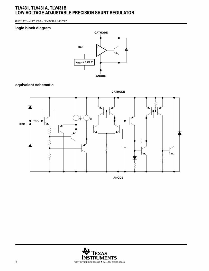
logic block diagramCATHODE
REF
ANODE
VREF = 1.24 V
−
+
equivalent schematic
REF
CATHODE
ANODE
TLV431, TLV431A, TLV431BLOW-VOLTAGE ADJUSTABLE PRECISION SHUNT REGULATOR
SLVS139T − JULY 1996 − REVISED JUNE 2007
5POST OFFICE BOX 655303 • DALLAS, TEXAS 75265
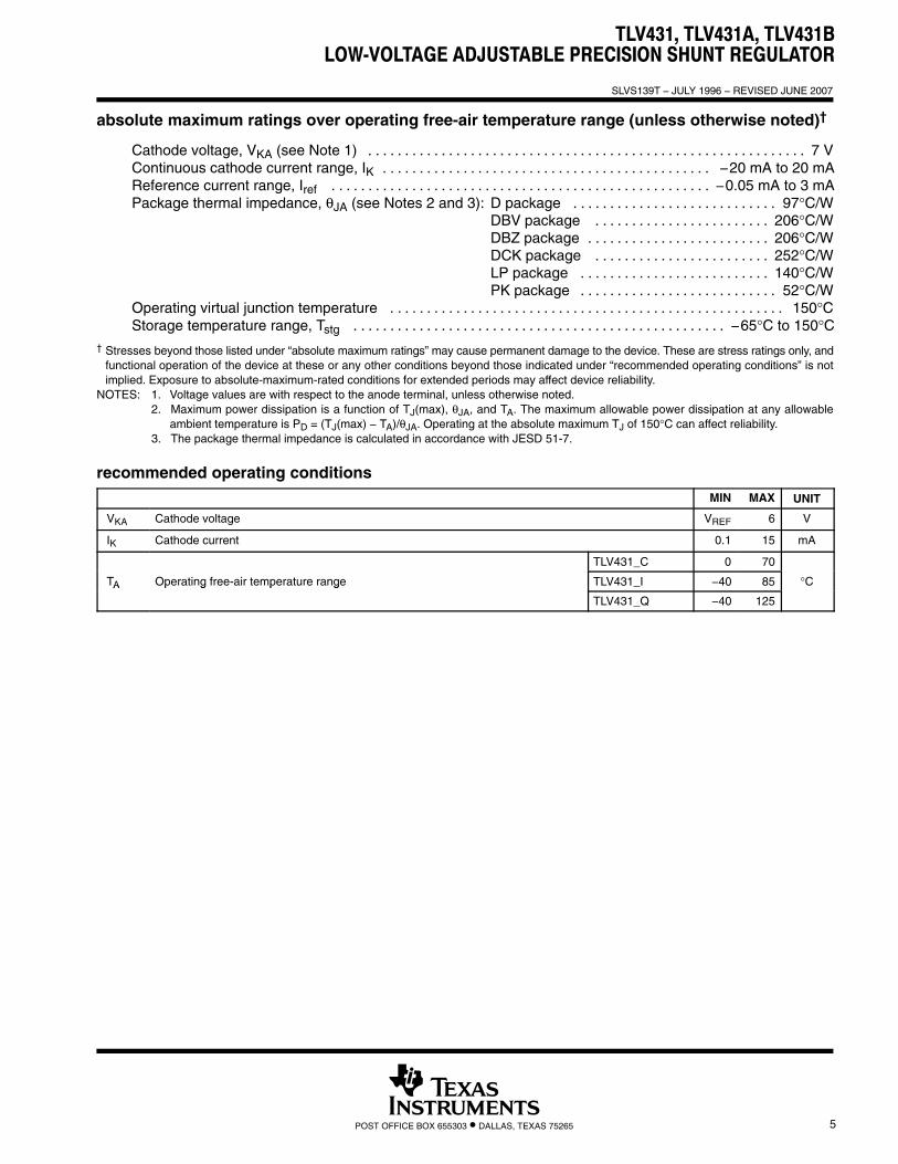
absolute maximum ratings over operating free-air temperature range (unless otherwise noted)†
Cathode voltage, VKA (see Note 1) 7 V. . . . . . . . . . . . . . . . . . . . . . . . . . . . . . . . . . . . . . . . . . . . . . . . . . . . . . . . . . . . Continuous cathode current range, IK −20 mA to 20 mA. . . . . . . . . . . . . . . . . . . . . . . . . . . . . . . . . . . . . . . . . . . . . Reference current range, Iref −0.05 mA to 3 mA. . . . . . . . . . . . . . . . . . . . . . . . . . . . . . . . . . . . . . . . . . . . . . . . . . . . Package thermal impedance, θJA (see Notes 2 and 3): D package 97°C/W. . . . . . . . . . . . . . . . . . . . . . . . . . . .
DBV package 206°C/W. . . . . . . . . . . . . . . . . . . . . . . . DBZ package 206°C/W. . . . . . . . . . . . . . . . . . . . . . . . . DCK package 252°C/W. . . . . . . . . . . . . . . . . . . . . . . . LP package 140°C/W. . . . . . . . . . . . . . . . . . . . . . . . . . PK package 52°C/W. . . . . . . . . . . . . . . . . . . . . . . . . . .
Operating virtual junction temperature 150°C. . . . . . . . . . . . . . . . . . . . . . . . . . . . . . . . . . . . . . . . . . . . . . . . . . . . . . Storage temperature range, Tstg −65°C to 150°C. . . . . . . . . . . . . . . . . . . . . . . . . . . . . . . . . . . . . . . . . . . . . . . . . . .
† Stresses beyond those listed under “absolute maximum ratings” may cause permanent damage to the device. These are stress ratings only, andfunctional operation of the device at these or any other conditions beyond those indicated under “recommended operating conditions” is notimplied. Exposure to absolute-maximum-rated conditions for extended periods may affect device reliability.
NOTES: 1. Voltage values are with respect to the anode terminal, unless otherwise noted.2. Maximum power dissipation is a function of TJ(max), θJA, and TA. The maximum allowable power dissipation at any allowable
ambient temperature is PD = (TJ(max) − TA)/θJA. Operating at the absolute maximum TJ of 150°C can affect reliability.3. The package thermal impedance is calculated in accordance with JESD 51-7.
recommended operating conditionsMIN MAX UNIT
VKA Cathode voltage VREF 6 V
IK Cathode current 0.1 15 mA
TLV431_C 0 70
TA Operating free-air temperature range TLV431_I −40 85 °CA p g p g
TLV431_Q −40 125
TLV431, TLV431A, TLV431BLOW-VOLTAGE ADJUSTABLE PRECISION SHUNT REGULATOR
SLVS139T − JULY 1996 − REVISED JUNE 2007
6 POST OFFICE BOX 655303 • DALLAS, TEXAS 75265
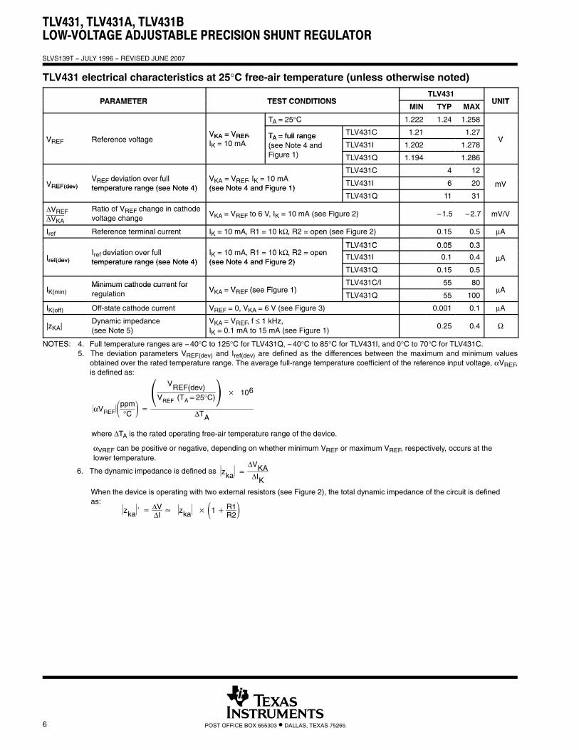
TLV431 electrical characteristics at 25°C free-air temperature (unless otherwise noted)
PARAMETER TEST CONDITIONSTLV431
UNITPARAMETER TEST CONDITIONSMIN TYP MAX
UNIT
TA = 25°C 1.222 1.24 1.258
V Reference voltageVKA = VREF, TA = full range TLV431C 1.21 1.27
VVREF Reference voltageVKA = VREF,IK = 10 mA
TA = full range(see Note 4 and TLV431I 1.202 1.278
V(see Note 4 andFigure 1) TLV431Q 1.194 1.286
V d i ti f ll V V I 10 ATLV431C 4 12
VREF(dev)VREF deviation over fulltemperature range (see Note 4)
VKA = VREF, IK = 10 mA(see Note 4 and Figure 1)
TLV431I 6 20 mVVREF(dev) temperature range (see Note 4) (see Note 4 and Figure 1)TLV431Q 11 31
mV
∆VREF∆VKA
Ratio of VREF change in cathodevoltage change
VKA = VREF to 6 V, IK = 10 mA (see Figure 2) −1.5 −2.7 mV/V
Iref Reference terminal current IK = 10 mA, R1 = 10 kΩ, R2 = open (see Figure 2) 0.15 0.5 µA
TLV431C 0 05 0 3I d i ti f ll I 10 A R1 10 kΩ R2
TLV431C 0.05 0.3
Iref(dev)Iref deviation over fulltemperature range (see Note 4)
IK = 10 mA, R1 = 10 kΩ, R2 = open(see Note 4 and Figure 2)
TLV431I 0.1 0.4 µAIref(dev) temperature range (see Note 4) (see Note 4 and Figure 2)TLV431Q 0.15 0.5
µA
IMinimum cathode current for
V V (see Figure 1)TLV431C/I 55 80
AIK(min)Minimum cathode current forregulation VKA = VREF (see Figure 1)
TLV431Q 55 100µA
IK(off) Off-state cathode current VREF = 0, VKA = 6 V (see Figure 3) 0.001 0.1 µA
|zKA|Dynamic impedance(see Note 5)
VKA = VREF, f ≤ 1 kHz,IK = 0.1 mA to 15 mA (see Figure 1)
0.25 0.4 Ω
NOTES: 4. Full temperature ranges are −40°C to 125°C for TLV431Q, −40°C to 85°C for TLV431I, and 0°C to 70°C for TLV431C.5. The deviation parameters VREF(dev) and Iref(dev) are defined as the differences between the maximum and minimum values
obtained over the rated temperature range. The average full-range temperature coefficient of the reference input voltage, αVREF,is defined as:
αVREFppm
°C VREF(dev)
VREF (TA25°C) 106
∆TA
where ∆TA is the rated operating free-air temperature range of the device.
αVREF can be positive or negative, depending on whether minimum VREF or maximum VREF, respectively, occurs at thelower temperature.
6. The dynamic impedance is defined as zka
∆VKA∆IK
When the device is operating with two external resistors (see Figure 2), the total dynamic impedance of the circuit is definedas: zka
∆V∆I
zka 1 R1
R2
TLV431, TLV431A, TLV431BLOW-VOLTAGE ADJUSTABLE PRECISION SHUNT REGULATOR
SLVS139T − JULY 1996 − REVISED JUNE 2007
7POST OFFICE BOX 655303 • DALLAS, TEXAS 75265
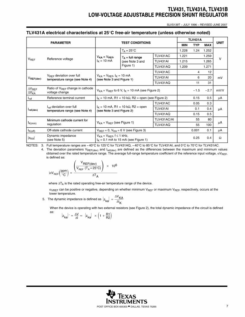
TLV431A electrical characteristics at 25°C free-air temperature (unless otherwise noted)
PARAMETER TEST CONDITIONSTLV431A
UNITPARAMETER TEST CONDITIONSMIN TYP MAX
UNIT
TA = 25°C 1.228 1.24 1.252
V Reference voltageVKA = VREF, TA = full range TLV431AC 1.221 1.259
VVREF Reference voltageVKA = VREF,IK = 10 mA
TA = full range(see Note 3 and TLV431AI 1.215 1.265
V(see Note 3 andFigure 1) TLV431AQ 1.209 1.271
V d i ti f ll V V I 10 ATLV431AC 4 12
VREF(dev)VREF deviation over fulltemperature range (see Note 4)
VKA = VREF, IK = 10 mA(see Note 3 and Figure 1)
TLV431AI 6 20 mVVREF(dev) temperature range (see Note 4) (see Note 3 and Figure 1)TLV431AQ 11 31
mV
∆VREF∆VKA
Ratio of VREF change in cathodevoltage change
VKA = VREF to 6 V, IK = 10 mA (see Figure 2) −1.5 −2.7 mV/V
Iref Reference terminal current IK = 10 mA, R1 = 10 kΩ, R2 = open (see Figure 2) 0.15 0.5 µA
I d i ti f ll I 10 A R1 10 kΩ R2TLV431AC 0.05 0.3
Iref(dev)Iref deviation over fulltemperature range (see Note 4)
IK = 10 mA, R1 = 10 kΩ, R2 = open(see Note 3 and Figure 2)
TLV431AI 0.1 0.4 µAIref(dev) temperature range (see Note 4) (see Note 3 and Figure 2)TLV431AQ 0.15 0.5
µA
IMinimum cathode current for
V V (see Figure 1)TLV431AC/AI 55 80
AIK(min)Minimum cathode current forregulation VKA = VREF (see Figure 1)
TLV431AQ 55 100µA
IK(off) Off-state cathode current VREF = 0, VKA = 6 V (see Figure 3) 0.001 0.1 µA
|zKA|Dynamic impedance(see Note 5)
VKA = VREF, f ≤ 1 kHz,IK = 0.1 mA to 15 mA (see Figure 1)
0.25 0.4 Ω
NOTES: 3. Full temperature ranges are −40°C to 125°C for TLV431AQ, −40°C to 85°C for TLV431AI, and 0°C to 70°C for TLV431AC.4. The deviation parameters VREF(dev) and Iref(dev) are defined as the differences between the maximum and minimum values
obtained over the rated temperature range. The average full-range temperature coefficient of the reference input voltage, αVREF,is defined as:
αVREFppm
°C VREF(dev)
VREF (TA25°C) 106
∆TA
where ∆TA is the rated operating free-air temperature range of the device.
αVREF can be positive or negative, depending on whether minimum VREF or maximum VREF, respectively, occurs at thelower temperature.
5. The dynamic impedance is defined as zka
∆VKA∆IK
When the device is operating with two external resistors (see Figure 2), the total dynamic impedance of the circuit is definedas: zka
∆V∆I
zka 1 R1
R2
TLV431, TLV431A, TLV431BLOW-VOLTAGE ADJUSTABLE PRECISION SHUNT REGULATOR
SLVS139T − JULY 1996 − REVISED JUNE 2007
8 POST OFFICE BOX 655303 • DALLAS, TEXAS 75265
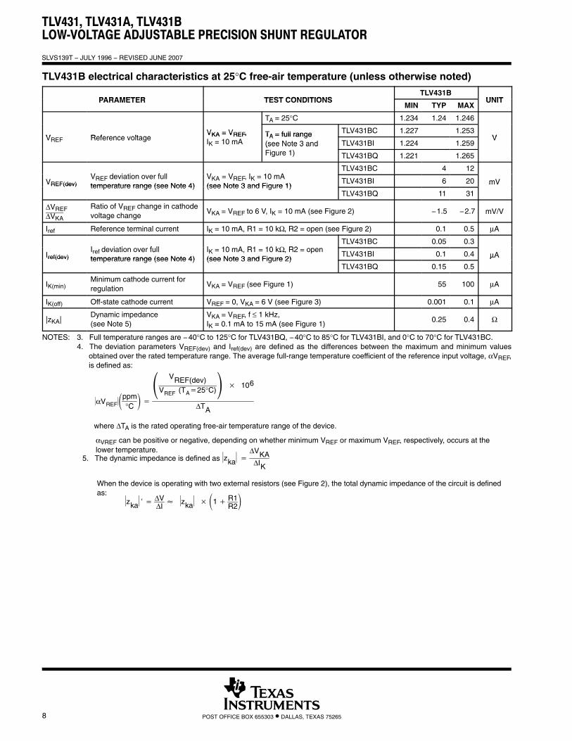
TLV431B electrical characteristics at 25°C free-air temperature (unless otherwise noted)
PARAMETER TEST CONDITIONSTLV431B
UNITPARAMETER TEST CONDITIONSMIN TYP MAX
UNIT
TA = 25°C 1.234 1.24 1.246
V Reference voltageVKA = VREF, TA = full range TLV431BC 1.227 1.253
VVREF Reference voltageVKA = VREF,IK = 10 mA
TA = full range(see Note 3 and TLV431BI 1.224 1.259
V(see Note 3 andFigure 1) TLV431BQ 1.221 1.265
V d i ti f ll V V I 10 ATLV431BC 4 12
VREF(dev)VREF deviation over fulltemperature range (see Note 4)
VKA = VREF, IK = 10 mA(see Note 3 and Figure 1)
TLV431BI 6 20 mVVREF(dev) temperature range (see Note 4) (see Note 3 and Figure 1)TLV431BQ 11 31
mV
∆VREF∆VKA
Ratio of VREF change in cathodevoltage change
VKA = VREF to 6 V, IK = 10 mA (see Figure 2) −1.5 −2.7 mV/V
Iref Reference terminal current IK = 10 mA, R1 = 10 kΩ, R2 = open (see Figure 2) 0.1 0.5 µA
I d i ti f ll I 10 A R1 10 kΩ R2TLV431BC 0.05 0.3
Iref(dev)Iref deviation over fulltemperature range (see Note 4)
IK = 10 mA, R1 = 10 kΩ, R2 = open(see Note 3 and Figure 2)
TLV431BI 0.1 0.4 µAIref(dev) temperature range (see Note 4) (see Note 3 and Figure 2)TLV431BQ 0.15 0.5
µA
IK(min)Minimum cathode current forregulation
VKA = VREF (see Figure 1) 55 100 µA
IK(off) Off-state cathode current VREF = 0, VKA = 6 V (see Figure 3) 0.001 0.1 µA
|zKA|Dynamic impedance(see Note 5)
VKA = VREF, f ≤ 1 kHz,IK = 0.1 mA to 15 mA (see Figure 1)
0.25 0.4 Ω
NOTES: 3. Full temperature ranges are −40°C to 125°C for TLV431BQ, −40°C to 85°C for TLV431BI, and 0°C to 70°C for TLV431BC.4. The deviation parameters VREF(dev) and Iref(dev) are defined as the differences between the maximum and minimum values
obtained over the rated temperature range. The average full-range temperature coefficient of the reference input voltage, αVREF,is defined as:
αVREFppm
°C VREF(dev)
VREF (TA25°C) 106
∆TA
where ∆TA is the rated operating free-air temperature range of the device.
αVREF can be positive or negative, depending on whether minimum VREF or maximum VREF, respectively, occurs at thelower temperature.
5. The dynamic impedance is defined as zka
∆VKA∆IK
When the device is operating with two external resistors (see Figure 2), the total dynamic impedance of the circuit is definedas: zka
∆V∆I
zka 1 R1
R2
TLV431, TLV431A, TLV431BLOW-VOLTAGE ADJUSTABLE PRECISION SHUNT REGULATOR
SLVS139T − JULY 1996 − REVISED JUNE 2007
9POST OFFICE BOX 655303 • DALLAS, TEXAS 75265
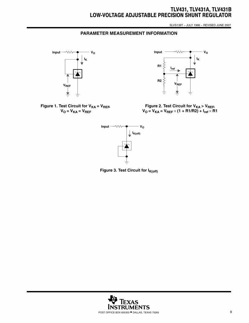
PARAMETER MEASUREMENT INFORMATION
VREF
Input VO
IK
Figure 1. Test Circuit for VKA = VREF, VO = VKA = VREF
Iref
IK
VOInput
VREF
R1
R2
Figure 2. Test Circuit for VKA > VREF,VO = VKA = VREF × (1 + R1/R2) + Iref × R1
IK(off)
VOInput
Figure 3. Test Circuit for IK(off)
TLV431, TLV431A, TLV431BLOW-VOLTAGE ADJUSTABLE PRECISION SHUNT REGULATOR
SLVS139T − JULY 1996 − REVISED JUNE 2007
10 POST OFFICE BOX 655303 • DALLAS, TEXAS 75265
PARAMETER MEASUREMENT INFORMATION†
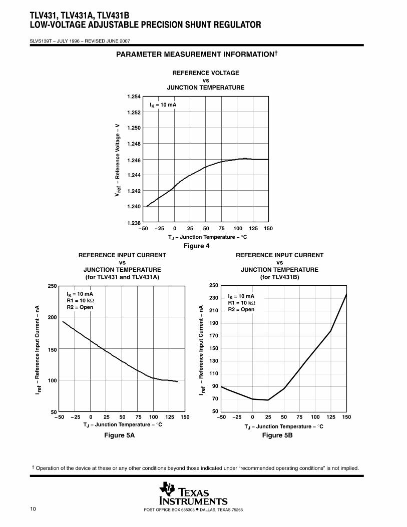
Figure 4
1.246
1.242
1.240
1.238
− R
efer
ence
Vo
ltag
e −
V 1.250
1.252
REFERENCE VOLTAGEvs
JUNCTION TEMPERATURE1.254
1.248
1.244
−50 −25 0 25 50 75 100 125 150
IK = 10 mA
Vre
f
TJ − Junction Temperature − °C
50
70
90
110
130
150
170
190
210
230
250
−50 −25 0 25 50 75 100 125 150
IK = 10 mAR1 = 10 kΩR2 = Open
− R
efer
ence
Inp
ut
Cu
rren
t −
nA
I ref
TJ − Junction Temperature − °CFigure 5
150
100
50
− R
efer
ence
Inp
ut
Cu
rren
t −
nA
200
REFERENCE INPUT CURRENTvs
JUNCTION TEMPERATURE(for TLV431 and TLV431A)
250
−50 −25 0 25 50 75 100 125 150
I ref
TJ − Junction Temperature − °C
IK = 10 mAR1 = 10 kΩR2 = Open
REFERENCE INPUT CURRENTvs
JUNCTION TEMPERATURE(for TLV431B)
Figure 5A Figure 5B
† Operation of the device at these or any other conditions beyond those indicated under “recommended operating conditions” is not implied.
TLV431, TLV431A, TLV431BLOW-VOLTAGE ADJUSTABLE PRECISION SHUNT REGULATOR
SLVS139T − JULY 1996 − REVISED JUNE 2007
11POST OFFICE BOX 655303 • DALLAS, TEXAS 75265
PARAMETER MEASUREMENT INFORMATION†
Figure 6
− C
ath
od
e C
urr
ent
− m
A
CATHODE CURRENTvs
CATHODE VOLTAGE15
10
5
0
−5
−10
−15−1 −0.5 0 0.5 1 1.5
I K
VKA = VREFTA = 25°C
VKA − Cathode Voltage − V
Figure 7
− C
ath
od
e C
urr
ent
−
CATHODE CURRENTvs
CATHODE VOLTAGE
250
200
150
100
50
0
−200
−250−1 −0.5 0 0.5 1 1.5
I KA
µ
VKA − Cathode Voltage − V
−50
−100
−150
VKA = VREFTA = 25°C
Figure 8
20
10
0
− O
ff-S
tate
Cat
ho
de
Cu
rren
t −
nA
30
OFF-STATE CATHODE CURRENTvs
JUNCTION TEMPERATURE(for TLV431 and TLV431A)
40
−50 −25 0 25 50 75 100 125
I K(o
ff)
TJ − Junction Temperature − °C
VKA = 5 VVREF = 0
150
OFF-STATE CATHODE CURRENTvs
JUNCTION TEMPERATURE(for TLV431B)
0
500
1000
1500
2000
2500
3000
−50 −25 0 25 50 75 100 125 150
VKA = 6 VVREF = 0
Figure 8BFigure 8ATJ − Junction Temperature − °C
− O
ff-S
tate
Cat
ho
de
Cu
rren
t −
nA
I K(o
ff)
† Operation of the device at these or any other conditions beyond those indicated under “recommended operating conditions” is not implied.
TLV431, TLV431A, TLV431BLOW-VOLTAGE ADJUSTABLE PRECISION SHUNT REGULATOR
SLVS139T − JULY 1996 − REVISED JUNE 2007
12 POST OFFICE BOX 655303 • DALLAS, TEXAS 75265
PARAMETER MEASUREMENT INFORMATION†
− R
atio
of
Del
ta R
efer
ence
Vo
ltag
e
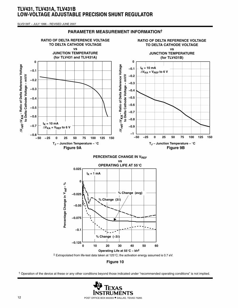
RATIO OF DELTA REFERENCE VOLTAGETO DELTA CATHODE VOLTAGE
vsJUNCTION TEMPERATURE(for TLV431 and TLV431A)
0
−0.1
−0.2
−0.3
−0.4
−0.5
−0.6
−0.7
−0.8
to D
elta
Cat
ho
de
Volt
age
− m
V/V
Vre
f/∆
VK
A∆
−50 −25 0 25 50 75 100 125 150
TJ − Junction Temperature − °C
Figure 9
IK = 10 mA∆VKA = VREF to 6 V
RATIO OF DELTA REFERENCE VOLTAGETO DELTA CATHODE VOLTAGE
vsJUNCTION TEMPERATURE
(for TLV431B)
−1.0
−0.9
−0.8
−0.7
−0.6
−0.5
−0.4
−0.3
−0.2
−0.1
0.0
−50 −25 0 25 50 75 100 125 150
IK = 10 mA∆VKA = VREF to 6 V
Figure 9BFigure 9A
−1
0
TJ − Junction Temperature − °C
− R
atio
of
Del
ta R
efer
ence
Vo
ltag
e
to D
elta
Cat
ho
de
Volt
age
− m
V/V
Vre
f/∆
VK
A∆
−0.025
−0.075
−0.1
−0.125
Per
cen
tag
e C
han
ge
in V
ref
− %
0.025
PERCENTAGE CHANGE IN VREFvs
OPERATING LIFE AT 55°C
0
−0.05
0 10 20 30 40 50 60
IK = 1 mA
Vre
f
Operating Life at 55°C − kh‡
% Change (3δ)
% Change (−3δ)
% Change (avg)
‡ Extrapolated from life-test data taken at 125°C; the activation energy assumed is 0.7 eV.
Figure 10
† Operation of the device at these or any other conditions beyond those indicated under “recommended operating conditions” is not implied.
TLV431, TLV431A, TLV431BLOW-VOLTAGE ADJUSTABLE PRECISION SHUNT REGULATOR
SLVS139T − JULY 1996 − REVISED JUNE 2007
13POST OFFICE BOX 655303 • DALLAS, TEXAS 75265
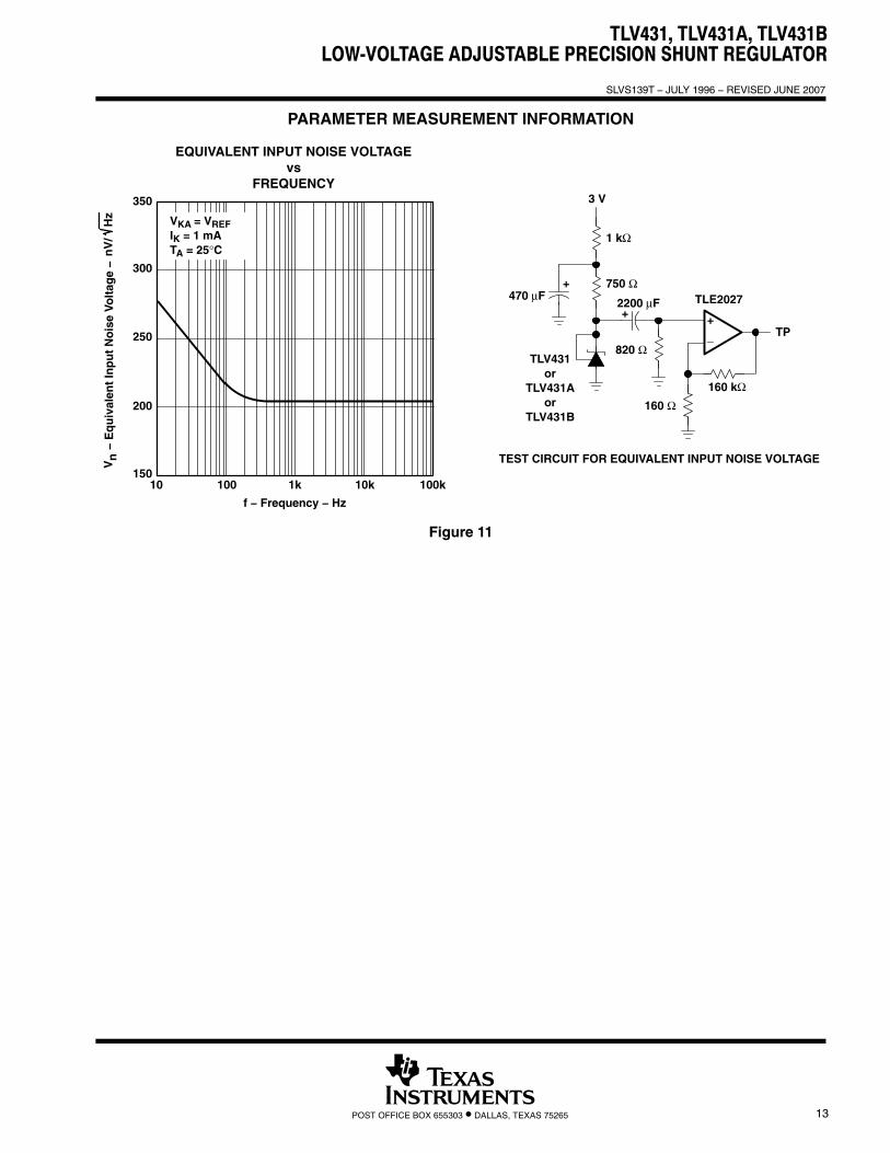
PARAMETER MEASUREMENT INFORMATION
200
15010 100 1k
− E
qu
ival
ent
Inp
ut
No
ise
Volt
age
−
f − Frequency − Hz
EQUIVALENT INPUT NOISE VOLTAGEvs
FREQUENCY350
10k 100k
300
250
Vn
nV
/H
z VKA = VREFIK = 1 mATA = 25°C
_+
820 Ω
+2200 µF
750 Ω
1 kΩ
470 µF
3 V
TLV431or
TLV431Aor
TLV431B
TP
160 kΩ160 Ω
TLE2027
TEST CIRCUIT FOR EQUIVALENT INPUT NOISE VOLTAGE
+
Figure 11
TLV431, TLV431A, TLV431BLOW-VOLTAGE ADJUSTABLE PRECISION SHUNT REGULATOR
SLVS139T − JULY 1996 − REVISED JUNE 2007
14 POST OFFICE BOX 655303 • DALLAS, TEXAS 75265
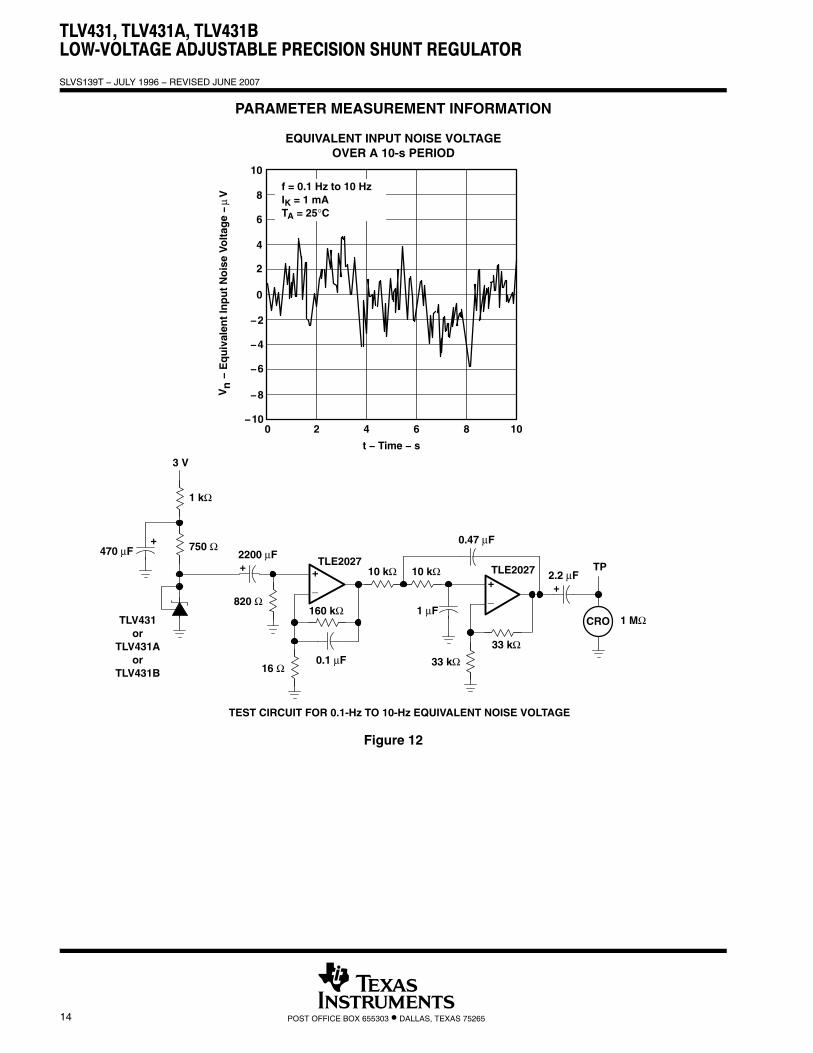
PARAMETER MEASUREMENT INFORMATION
0 2 4 6
t − Time − s
EQUIVALENT INPUT NOISE VOLTAGEOVER A 10-s PERIOD
8 10
10
8
6
4
2
0
−2
−4
−6
−8
−10
f = 0.1 Hz to 10 HzIK = 1 mATA = 25°C
− E
qu
ival
ent
Inp
ut
No
ise
Volt
age
−V
nV
µ
_+
1 µF
750 Ω
1 kΩ
470 µF
3 V
TLV431or
TLV431Aor
TLV431B
33 kΩ
TLE2027
TEST CIRCUIT FOR 0.1-Hz TO 10-Hz EQUIVALENT NOISE VOLTAGE
+
33 kΩ
10 kΩ_+
16 Ω0.1 µF
160 kΩ820 Ω
+2200 µF
TP2.2 µF
CRO 1 MΩ
TLE2027
0.47 µF
10 kΩ
+
Figure 12
TLV431, TLV431A, TLV431BLOW-VOLTAGE ADJUSTABLE PRECISION SHUNT REGULATOR
SLVS139T − JULY 1996 − REVISED JUNE 2007
15POST OFFICE BOX 655303 • DALLAS, TEXAS 75265
PARAMETER MEASUREMENT INFORMATION
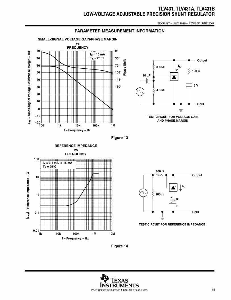
SMALL-SIGNAL VOLTAGE GAIN/PHASE MARGINvs
FREQUENCY
10 µF
GND
Output
180 Ω
IK6.8 kΩ
1k 10k 100k 1M100
− S
mal
l-S
ign
al V
olt
age
Gai
n/P
has
e M
arg
in −
dB
f − Frequency − Hz
AV
TEST CIRCUIT FOR VOLTAGE GAINAND PHASE MARGIN
80
70
60
50
40
30
20
10
0
−10
0°
36°
72°
108°
144°
180°
Ph
ase
Sh
ift
4.3 kΩ5 V
IK = 10 mATA = 25°C
−20
Figure 13
100 Ω
100 Ω
GND
Output
IK
0.1
1k 10k 100k 1M 10M
− R
efer
ence
Imp
edan
ce −
1
f − Frequency − Hz
REFERENCE IMPEDANCEvs
FREQUENCY
10
100
ka|z
|Ω
IK = 0.1 mA to 15 mATA = 25°C
TEST CIRCUIT FOR REFERENCE IMPEDANCE
0.01
−
+
Figure 14
TLV431, TLV431A, TLV431BLOW-VOLTAGE ADJUSTABLE PRECISION SHUNT REGULATOR
SLVS139T − JULY 1996 − REVISED JUNE 2007
16 POST OFFICE BOX 655303 • DALLAS, TEXAS 75265
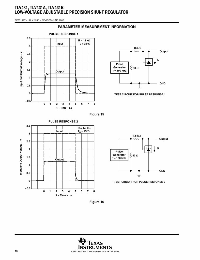
PARAMETER MEASUREMENT INFORMATION
Inp
ut
and
Ou
tpu
t Vo
ltag
e −
V
Output
R = 18 kΩTA = 25°C
18 kΩ
50 Ω
GND
Output
PulseGeneratorf = 100 kHz
TEST CIRCUIT FOR PULSE RESPONSE 1
0 1 2 3 4
PULSE RESPONSE 1
5 6 7 8
3.5
3
2.5
2
1.5
1
0.5
0
−0.5
t − Time − µs
Input
Ik
Figure 15
Inp
ut
and
Ou
tpu
t Vo
ltag
e −
V
Output
R = 1.8 kΩTA = 25°C
1.8 kΩ
50 Ω
GND
Output
PulseGeneratorf = 100 kHz
TEST CIRCUIT FOR PULSE RESPONSE 2
0 1 2 3 4
PULSE RESPONSE 2
5 6 7 8
3.5
3
2.5
2
1.5
1
0.5
0
−0.5
t − Time − µs
Input
IK
Figure 16
TLV431, TLV431A, TLV431BLOW-VOLTAGE ADJUSTABLE PRECISION SHUNT REGULATOR
SLVS139T − JULY 1996 − REVISED JUNE 2007
17POST OFFICE BOX 655303 • DALLAS, TEXAS 75265
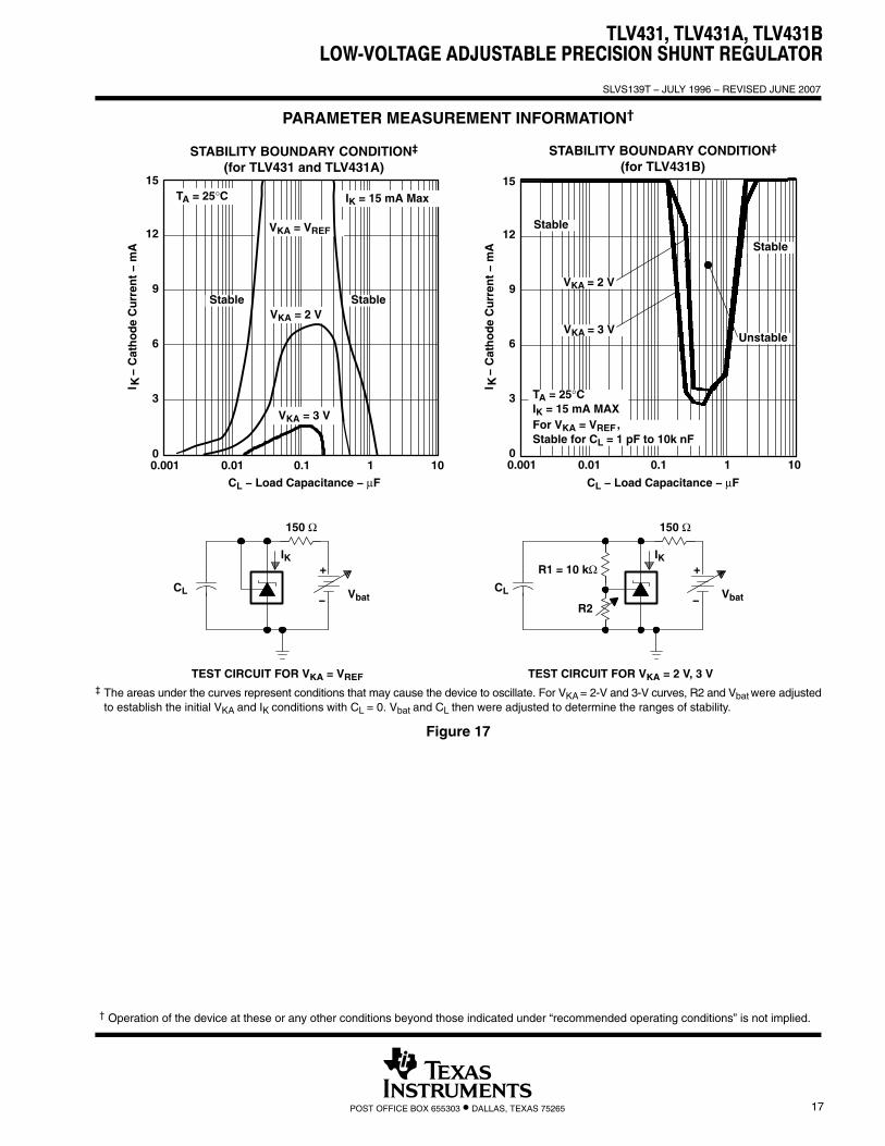
PARAMETER MEASUREMENT INFORMATION†
9
6
0
15
0.001 0.01 0.1 1 10
− C
ath
od
e C
urr
ent
− m
A
12
STABILITY BOUNDARY CONDITION‡
(for TLV431 and TLV431A)
3
I K
CL − Load Capacitance − µF
Stable
VKA = VREF
VKA = 2 VStable
VKA = 3 V
TA = 25°C
150 Ω
CL Vbat
IK
TEST CIRCUIT FOR VKA = VREF
150 Ω
CL Vbat
IKR1 = 10 kΩ
R2
TEST CIRCUIT FOR VKA = 2 V, 3 V
−
+
−
+
IK = 15 mA Max
− C
ath
od
e C
urr
ent
− m
A
STABILITY BOUNDARY CONDITION‡
(for TLV431B)
I KCL − Load Capacitance − µF
9
6
0
15
0.001 0.01 0.1 1 10
12
3
Stable
VKA = 3 V
Stable
Unstable
VKA = 2 V
TA = 25°CIK = 15 mA MAXFor VKA = VREF ,Stable for CL = 1 pF to 10k nF
‡ The areas under the curves represent conditions that may cause the device to oscillate. For VKA = 2-V and 3-V curves, R2 and Vbat were adjustedto establish the initial VKA and IK conditions with CL = 0. Vbat and CL then were adjusted to determine the ranges of stability.
Figure 17
† Operation of the device at these or any other conditions beyond those indicated under “recommended operating conditions” is not implied.
TLV431, TLV431A, TLV431BLOW-VOLTAGE ADJUSTABLE PRECISION SHUNT REGULATOR
SLVS139T − JULY 1996 − REVISED JUNE 2007
18 POST OFFICE BOX 655303 • DALLAS, TEXAS 75265
APPLICATION INFORMATION
~
~
P
− +
P
P
VCC
VFB
CurrentSense
Gate Drive
GND
Controller
P
P P P
TLV431or
TLV431Aor
TLV431B
VO3.3 V
VI120 V
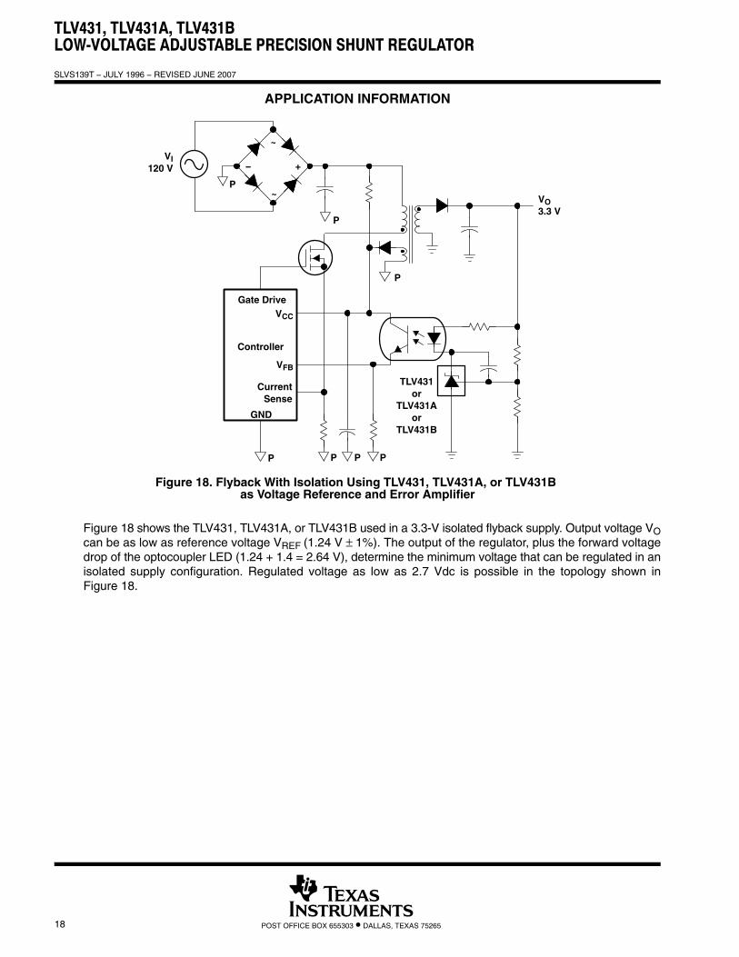
Figure 18. Flyback With Isolation Using TLV431, TLV431A, or TLV431B as Voltage Reference and Error Amplifier
Figure 18 shows the TLV431, TLV431A, or TLV431B used in a 3.3-V isolated flyback supply. Output voltage VOcan be as low as reference voltage VREF (1.24 V ± 1%). The output of the regulator, plus the forward voltagedrop of the optocoupler LED (1.24 + 1.4 = 2.64 V), determine the minimum voltage that can be regulated in anisolated supply configuration. Regulated voltage as low as 2.7 Vdc is possible in the topology shown inFigure 18.
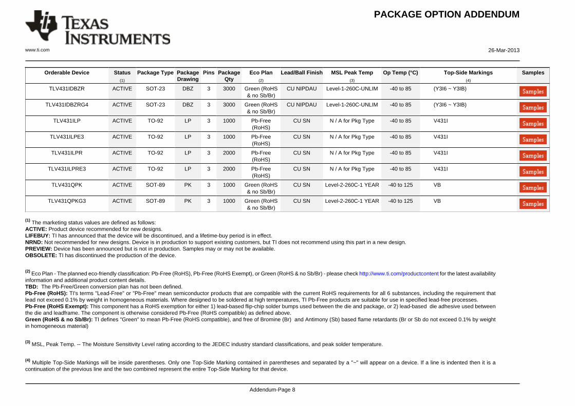
PACKAGE OPTION ADDENDUM
www.ti.com 26-Mar-2013
Addendum-Page 1
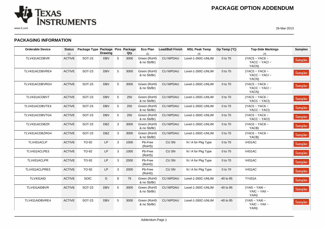
PACKAGING INFORMATION
Orderable Device Status(1)
Package Type PackageDrawing
Pins PackageQty
Eco Plan(2)
Lead/Ball Finish MSL Peak Temp(3)
Op Temp (°C) Top-Side Markings(4)
Samples
TLV431ACDBVR ACTIVE SOT-23 DBV 5 3000 Green (RoHS& no Sb/Br)
CU NIPDAU Level-1-260C-UNLIM 0 to 70 (YAC5 ~ YAC6 ~ YACC ~ YACI ~ YACN)
TLV431ACDBVRE4 ACTIVE SOT-23 DBV 5 3000 Green (RoHS& no Sb/Br)
CU NIPDAU Level-1-260C-UNLIM 0 to 70 (YAC5 ~ YAC6 ~ YACC ~ YACI ~ YACN)
TLV431ACDBVRG4 ACTIVE SOT-23 DBV 5 3000 Green (RoHS& no Sb/Br)
CU NIPDAU Level-1-260C-UNLIM 0 to 70 (YAC5 ~ YAC6 ~ YACC ~ YACI ~ YACN)
TLV431ACDBVT ACTIVE SOT-23 DBV 5 250 Green (RoHS& no Sb/Br)
CU NIPDAU Level-1-260C-UNLIM 0 to 70 (YAC5 ~ YAC6 ~ YACC ~ YACI)
TLV431ACDBVTE4 ACTIVE SOT-23 DBV 5 250 Green (RoHS& no Sb/Br)
CU NIPDAU Level-1-260C-UNLIM 0 to 70 (YAC5 ~ YAC6 ~ YACC ~ YACI)
TLV431ACDBVTG4 ACTIVE SOT-23 DBV 5 250 Green (RoHS& no Sb/Br)
CU NIPDAU Level-1-260C-UNLIM 0 to 70 (YAC5 ~ YAC6 ~ YACC ~ YACI)
TLV431ACDBZR ACTIVE SOT-23 DBZ 3 3000 Green (RoHS& no Sb/Br)
CU NIPDAU Level-1-260C-UNLIM 0 to 70 (YAC6 ~ YAC8 ~ YACB)
TLV431ACDBZRG4 ACTIVE SOT-23 DBZ 3 3000 Green (RoHS& no Sb/Br)
CU NIPDAU Level-1-260C-UNLIM 0 to 70 (YAC6 ~ YAC8 ~ YACB)
TLV431ACLP ACTIVE TO-92 LP 3 1000 Pb-Free(RoHS)
CU SN N / A for Pkg Type 0 to 70 V431AC
TLV431ACLPE3 ACTIVE TO-92 LP 3 1000 Pb-Free(RoHS)
CU SN N / A for Pkg Type 0 to 70 V431AC
TLV431ACLPR ACTIVE TO-92 LP 3 2000 Pb-Free(RoHS)
CU SN N / A for Pkg Type 0 to 70 V431AC
TLV431ACLPRE3 ACTIVE TO-92 LP 3 2000 Pb-Free(RoHS)
CU SN N / A for Pkg Type 0 to 70 V431AC
TLV431AID ACTIVE SOIC D 8 75 Green (RoHS& no Sb/Br)
CU NIPDAU Level-1-260C-UNLIM -40 to 85 TY431A
TLV431AIDBVR ACTIVE SOT-23 DBV 5 3000 Green (RoHS& no Sb/Br)
CU NIPDAU Level-1-260C-UNLIM -40 to 85 (YAI5 ~ YAI6 ~ YAIC ~ YAII ~ YAIN)
TLV431AIDBVRE4 ACTIVE SOT-23 DBV 5 3000 Green (RoHS& no Sb/Br)
CU NIPDAU Level-1-260C-UNLIM -40 to 85 (YAI5 ~ YAI6 ~ YAIC ~ YAII ~ YAIN)
PACKAGE OPTION ADDENDUM
www.ti.com 26-Mar-2013
Addendum-Page 2
Orderable Device Status(1)
Package Type PackageDrawing
Pins PackageQty
Eco Plan(2)
Lead/Ball Finish MSL Peak Temp(3)
Op Temp (°C) Top-Side Markings(4)
Samples
TLV431AIDBVRG4 ACTIVE SOT-23 DBV 5 3000 Green (RoHS& no Sb/Br)
CU NIPDAU Level-1-260C-UNLIM -40 to 85 (YAI5 ~ YAI6 ~ YAIC ~ YAII ~ YAIN)
TLV431AIDBVT ACTIVE SOT-23 DBV 5 250 Green (RoHS& no Sb/Br)
CU NIPDAU Level-1-260C-UNLIM -40 to 85 (YAI5 ~ YAI6 ~ YAIC ~ YAII)
TLV431AIDBVTE4 ACTIVE SOT-23 DBV 5 250 Green (RoHS& no Sb/Br)
CU NIPDAU Level-1-260C-UNLIM -40 to 85 (YAI5 ~ YAI6 ~ YAIC ~ YAII)
TLV431AIDBVTG4 ACTIVE SOT-23 DBV 5 250 Green (RoHS& no Sb/Br)
CU NIPDAU Level-1-260C-UNLIM -40 to 85 (YAI5 ~ YAI6 ~ YAIC ~ YAII)
TLV431AIDBZR ACTIVE SOT-23 DBZ 3 3000 Green (RoHS& no Sb/Br)
CU NIPDAU Level-1-260C-UNLIM -40 to 85 (YAI6 ~ YAI8 ~ YAIB)
TLV431AIDBZRG4 ACTIVE SOT-23 DBZ 3 3000 Green (RoHS& no Sb/Br)
CU NIPDAU Level-1-260C-UNLIM -40 to 85 (YAI6 ~ YAI8 ~ YAIB)
TLV431AIDE4 ACTIVE SOIC D 8 75 Green (RoHS& no Sb/Br)
CU NIPDAU Level-1-260C-UNLIM -40 to 85 TY431A
TLV431AIDG4 ACTIVE SOIC D 8 75 Green (RoHS& no Sb/Br)
CU NIPDAU Level-1-260C-UNLIM -40 to 85 TY431A
TLV431AIDR ACTIVE SOIC D 8 2500 Green (RoHS& no Sb/Br)
CU NIPDAU Level-1-260C-UNLIM -40 to 85 TY431A
TLV431AIDRE4 ACTIVE SOIC D 8 2500 Green (RoHS& no Sb/Br)
CU NIPDAU Level-1-260C-UNLIM -40 to 85 TY431A
TLV431AIDRG4 ACTIVE SOIC D 8 2500 Green (RoHS& no Sb/Br)
CU NIPDAU Level-1-260C-UNLIM -40 to 85 TY431A
TLV431AILP ACTIVE TO-92 LP 3 1000 Pb-Free(RoHS)
CU SN N / A for Pkg Type -40 to 85 V431AI
TLV431AILPE3 ACTIVE TO-92 LP 3 1000 Pb-Free(RoHS)
CU SN N / A for Pkg Type -40 to 85 V431AI
TLV431AILPM ACTIVE TO-92 LP 3 2000 Pb-Free(RoHS)
CU SN N / A for Pkg Type -40 to 85 V431AI
TLV431AILPME3 ACTIVE TO-92 LP 3 2000 Pb-Free(RoHS)
CU SN N / A for Pkg Type -40 to 85 V431AI
TLV431AILPR ACTIVE TO-92 LP 3 2000 Pb-Free(RoHS)
CU SN N / A for Pkg Type -40 to 85 V431AI
TLV431AILPRE3 ACTIVE TO-92 LP 3 2000 Pb-Free(RoHS)
CU SN N / A for Pkg Type -40 to 85 V431AI
PACKAGE OPTION ADDENDUM
www.ti.com 26-Mar-2013
Addendum-Page 3
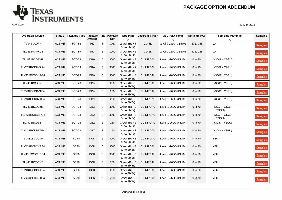
Orderable Device Status(1)
Package Type PackageDrawing
Pins PackageQty
Eco Plan(2)
Lead/Ball Finish MSL Peak Temp(3)
Op Temp (°C) Top-Side Markings(4)
Samples
TLV431AQPK ACTIVE SOT-89 PK 3 1000 Green (RoHS& no Sb/Br)
CU SN Level-2-260C-1 YEAR -40 to 125 VA
TLV431AQPKG3 ACTIVE SOT-89 PK 3 1000 Green (RoHS& no Sb/Br)
CU SN Level-2-260C-1 YEAR -40 to 125 VA
TLV431BCDBVR ACTIVE SOT-23 DBV 5 3000 Green (RoHS& no Sb/Br)
CU NIPDAU Level-1-260C-UNLIM 0 to 70 (Y3GG ~ Y3GU)
TLV431BCDBVRE4 ACTIVE SOT-23 DBV 5 3000 Green (RoHS& no Sb/Br)
CU NIPDAU Level-1-260C-UNLIM 0 to 70 (Y3GG ~ Y3GU)
TLV431BCDBVRG4 ACTIVE SOT-23 DBV 5 3000 Green (RoHS& no Sb/Br)
CU NIPDAU Level-1-260C-UNLIM 0 to 70 (Y3GG ~ Y3GU)
TLV431BCDBVT ACTIVE SOT-23 DBV 5 250 Green (RoHS& no Sb/Br)
CU NIPDAU Level-1-260C-UNLIM 0 to 70 (Y3GG ~ Y3GU)
TLV431BCDBVTE4 ACTIVE SOT-23 DBV 5 250 Green (RoHS& no Sb/Br)
CU NIPDAU Level-1-260C-UNLIM 0 to 70 (Y3GG ~ Y3GU)
TLV431BCDBVTG4 ACTIVE SOT-23 DBV 5 250 Green (RoHS& no Sb/Br)
CU NIPDAU Level-1-260C-UNLIM 0 to 70 (Y3GG ~ Y3GU)
TLV431BCDBZR ACTIVE SOT-23 DBZ 3 3000 Green (RoHS& no Sb/Br)
CU NIPDAU Level-1-260C-UNLIM 0 to 70 (Y3G3 ~ Y3GS ~ Y3GU)
TLV431BCDBZRG4 ACTIVE SOT-23 DBZ 3 3000 Green (RoHS& no Sb/Br)
CU NIPDAU Level-1-260C-UNLIM 0 to 70 (Y3G3 ~ Y3GS ~ Y3GU)
TLV431BCDBZT ACTIVE SOT-23 DBZ 3 250 Green (RoHS& no Sb/Br)
CU NIPDAU Level-1-260C-UNLIM 0 to 70 (Y3GS ~ Y3GU)
TLV431BCDBZTG4 ACTIVE SOT-23 DBZ 3 250 Green (RoHS& no Sb/Br)
CU NIPDAU Level-1-260C-UNLIM 0 to 70 (Y3GS ~ Y3GU)
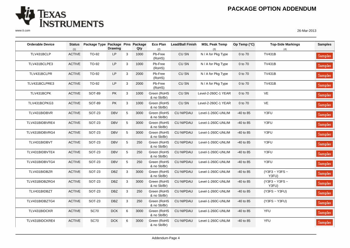
TLV431BCDCKR ACTIVE SC70 DCK 6 3000 Green (RoHS& no Sb/Br)
CU NIPDAU Level-1-260C-UNLIM 0 to 70 YEU
TLV431BCDCKRE4 ACTIVE SC70 DCK 6 3000 Green (RoHS& no Sb/Br)
CU NIPDAU Level-1-260C-UNLIM 0 to 70 YEU
TLV431BCDCKRG4 ACTIVE SC70 DCK 6 3000 Green (RoHS& no Sb/Br)
CU NIPDAU Level-1-260C-UNLIM 0 to 70 YEU
TLV431BCDCKT ACTIVE SC70 DCK 6 250 Green (RoHS& no Sb/Br)
CU NIPDAU Level-1-260C-UNLIM 0 to 70 YEU
TLV431BCDCKTE4 ACTIVE SC70 DCK 6 250 Green (RoHS& no Sb/Br)
CU NIPDAU Level-1-260C-UNLIM 0 to 70 YEU
TLV431BCDCKTG4 ACTIVE SC70 DCK 6 250 Green (RoHS& no Sb/Br)
CU NIPDAU Level-1-260C-UNLIM 0 to 70 YEU
PACKAGE OPTION ADDENDUM
www.ti.com 26-Mar-2013
Addendum-Page 4
Orderable Device Status(1)
Package Type PackageDrawing
Pins PackageQty
Eco Plan(2)
Lead/Ball Finish MSL Peak Temp(3)
Op Temp (°C) Top-Side Markings(4)
Samples
TLV431BCLP ACTIVE TO-92 LP 3 1000 Pb-Free(RoHS)
CU SN N / A for Pkg Type 0 to 70 TV431B
TLV431BCLPE3 ACTIVE TO-92 LP 3 1000 Pb-Free(RoHS)
CU SN N / A for Pkg Type 0 to 70 TV431B
TLV431BCLPR ACTIVE TO-92 LP 3 2000 Pb-Free(RoHS)
CU SN N / A for Pkg Type 0 to 70 TV431B
TLV431BCLPRE3 ACTIVE TO-92 LP 3 2000 Pb-Free(RoHS)
CU SN N / A for Pkg Type 0 to 70 TV431B
TLV431BCPK ACTIVE SOT-89 PK 3 1000 Green (RoHS& no Sb/Br)
CU SN Level-2-260C-1 YEAR 0 to 70 VE
TLV431BCPKG3 ACTIVE SOT-89 PK 3 1000 Green (RoHS& no Sb/Br)
CU SN Level-2-260C-1 YEAR 0 to 70 VE
TLV431BIDBVR ACTIVE SOT-23 DBV 5 3000 Green (RoHS& no Sb/Br)
CU NIPDAU Level-1-260C-UNLIM -40 to 85 Y3FU
TLV431BIDBVRE4 ACTIVE SOT-23 DBV 5 3000 Green (RoHS& no Sb/Br)
CU NIPDAU Level-1-260C-UNLIM -40 to 85 Y3FU
TLV431BIDBVRG4 ACTIVE SOT-23 DBV 5 3000 Green (RoHS& no Sb/Br)
CU NIPDAU Level-1-260C-UNLIM -40 to 85 Y3FU
TLV431BIDBVT ACTIVE SOT-23 DBV 5 250 Green (RoHS& no Sb/Br)
CU NIPDAU Level-1-260C-UNLIM -40 to 85 Y3FU
TLV431BIDBVTE4 ACTIVE SOT-23 DBV 5 250 Green (RoHS& no Sb/Br)
CU NIPDAU Level-1-260C-UNLIM -40 to 85 Y3FU
TLV431BIDBVTG4 ACTIVE SOT-23 DBV 5 250 Green (RoHS& no Sb/Br)
CU NIPDAU Level-1-260C-UNLIM -40 to 85 Y3FU
TLV431BIDBZR ACTIVE SOT-23 DBZ 3 3000 Green (RoHS& no Sb/Br)
CU NIPDAU Level-1-260C-UNLIM -40 to 85 (Y3F3 ~ Y3FS ~ Y3FU)
TLV431BIDBZRG4 ACTIVE SOT-23 DBZ 3 3000 Green (RoHS& no Sb/Br)
CU NIPDAU Level-1-260C-UNLIM -40 to 85 (Y3F3 ~ Y3FS ~ Y3FU)
TLV431BIDBZT ACTIVE SOT-23 DBZ 3 250 Green (RoHS& no Sb/Br)
CU NIPDAU Level-1-260C-UNLIM -40 to 85 (Y3FS ~ Y3FU)
TLV431BIDBZTG4 ACTIVE SOT-23 DBZ 3 250 Green (RoHS& no Sb/Br)
CU NIPDAU Level-1-260C-UNLIM -40 to 85 (Y3FS ~ Y3FU)
TLV431BIDCKR ACTIVE SC70 DCK 6 3000 Green (RoHS& no Sb/Br)
CU NIPDAU Level-1-260C-UNLIM -40 to 85 YFU
TLV431BIDCKRE4 ACTIVE SC70 DCK 6 3000 Green (RoHS& no Sb/Br)
CU NIPDAU Level-1-260C-UNLIM -40 to 85 YFU
PACKAGE OPTION ADDENDUM
www.ti.com 26-Mar-2013
Addendum-Page 5
Orderable Device Status(1)
Package Type PackageDrawing
Pins PackageQty
Eco Plan(2)
Lead/Ball Finish MSL Peak Temp(3)
Op Temp (°C) Top-Side Markings(4)
Samples
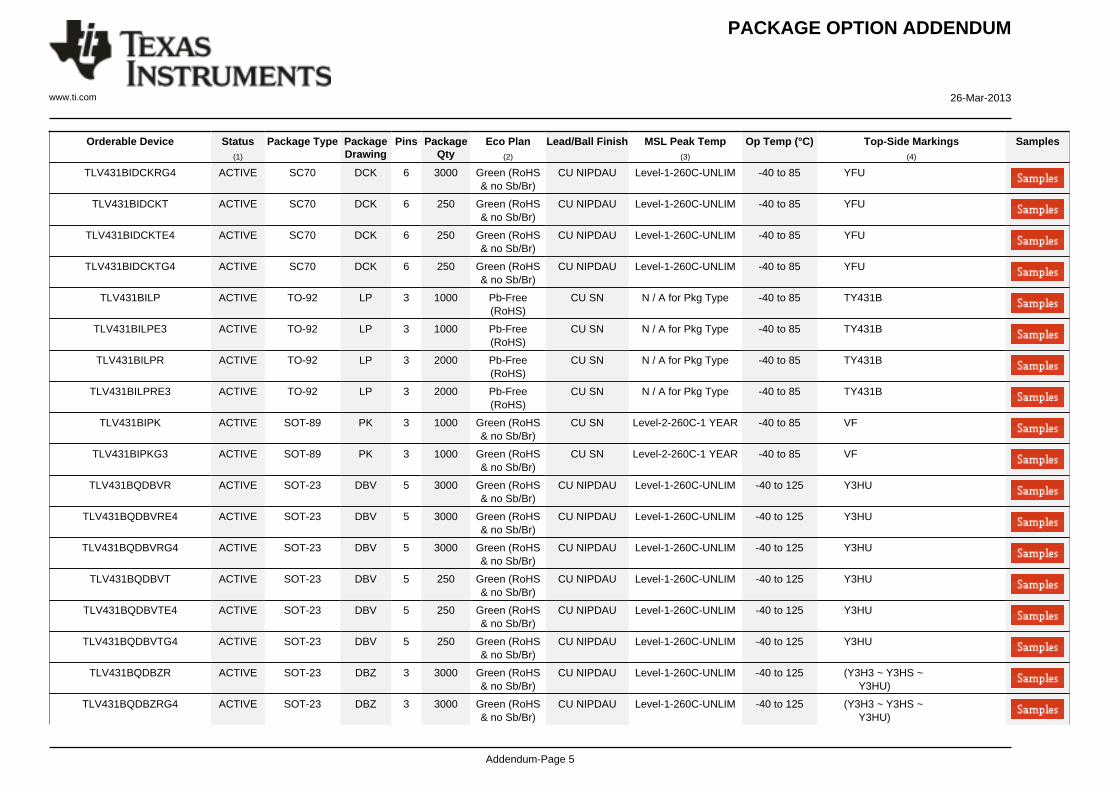
TLV431BIDCKRG4 ACTIVE SC70 DCK 6 3000 Green (RoHS& no Sb/Br)
CU NIPDAU Level-1-260C-UNLIM -40 to 85 YFU
TLV431BIDCKT ACTIVE SC70 DCK 6 250 Green (RoHS& no Sb/Br)
CU NIPDAU Level-1-260C-UNLIM -40 to 85 YFU
TLV431BIDCKTE4 ACTIVE SC70 DCK 6 250 Green (RoHS& no Sb/Br)
CU NIPDAU Level-1-260C-UNLIM -40 to 85 YFU
TLV431BIDCKTG4 ACTIVE SC70 DCK 6 250 Green (RoHS& no Sb/Br)
CU NIPDAU Level-1-260C-UNLIM -40 to 85 YFU
TLV431BILP ACTIVE TO-92 LP 3 1000 Pb-Free(RoHS)
CU SN N / A for Pkg Type -40 to 85 TY431B
TLV431BILPE3 ACTIVE TO-92 LP 3 1000 Pb-Free(RoHS)
CU SN N / A for Pkg Type -40 to 85 TY431B
TLV431BILPR ACTIVE TO-92 LP 3 2000 Pb-Free(RoHS)
CU SN N / A for Pkg Type -40 to 85 TY431B
TLV431BILPRE3 ACTIVE TO-92 LP 3 2000 Pb-Free(RoHS)
CU SN N / A for Pkg Type -40 to 85 TY431B
TLV431BIPK ACTIVE SOT-89 PK 3 1000 Green (RoHS& no Sb/Br)
CU SN Level-2-260C-1 YEAR -40 to 85 VF
TLV431BIPKG3 ACTIVE SOT-89 PK 3 1000 Green (RoHS& no Sb/Br)
CU SN Level-2-260C-1 YEAR -40 to 85 VF
TLV431BQDBVR ACTIVE SOT-23 DBV 5 3000 Green (RoHS& no Sb/Br)
CU NIPDAU Level-1-260C-UNLIM -40 to 125 Y3HU
TLV431BQDBVRE4 ACTIVE SOT-23 DBV 5 3000 Green (RoHS& no Sb/Br)
CU NIPDAU Level-1-260C-UNLIM -40 to 125 Y3HU
TLV431BQDBVRG4 ACTIVE SOT-23 DBV 5 3000 Green (RoHS& no Sb/Br)
CU NIPDAU Level-1-260C-UNLIM -40 to 125 Y3HU
TLV431BQDBVT ACTIVE SOT-23 DBV 5 250 Green (RoHS& no Sb/Br)
CU NIPDAU Level-1-260C-UNLIM -40 to 125 Y3HU
TLV431BQDBVTE4 ACTIVE SOT-23 DBV 5 250 Green (RoHS& no Sb/Br)
CU NIPDAU Level-1-260C-UNLIM -40 to 125 Y3HU
TLV431BQDBVTG4 ACTIVE SOT-23 DBV 5 250 Green (RoHS& no Sb/Br)
CU NIPDAU Level-1-260C-UNLIM -40 to 125 Y3HU
TLV431BQDBZR ACTIVE SOT-23 DBZ 3 3000 Green (RoHS& no Sb/Br)
CU NIPDAU Level-1-260C-UNLIM -40 to 125 (Y3H3 ~ Y3HS ~ Y3HU)
TLV431BQDBZRG4 ACTIVE SOT-23 DBZ 3 3000 Green (RoHS& no Sb/Br)
CU NIPDAU Level-1-260C-UNLIM -40 to 125 (Y3H3 ~ Y3HS ~ Y3HU)
PACKAGE OPTION ADDENDUM
www.ti.com 26-Mar-2013
Addendum-Page 6
Orderable Device Status(1)
Package Type PackageDrawing
Pins PackageQty
Eco Plan(2)
Lead/Ball Finish MSL Peak Temp(3)
Op Temp (°C) Top-Side Markings(4)
Samples
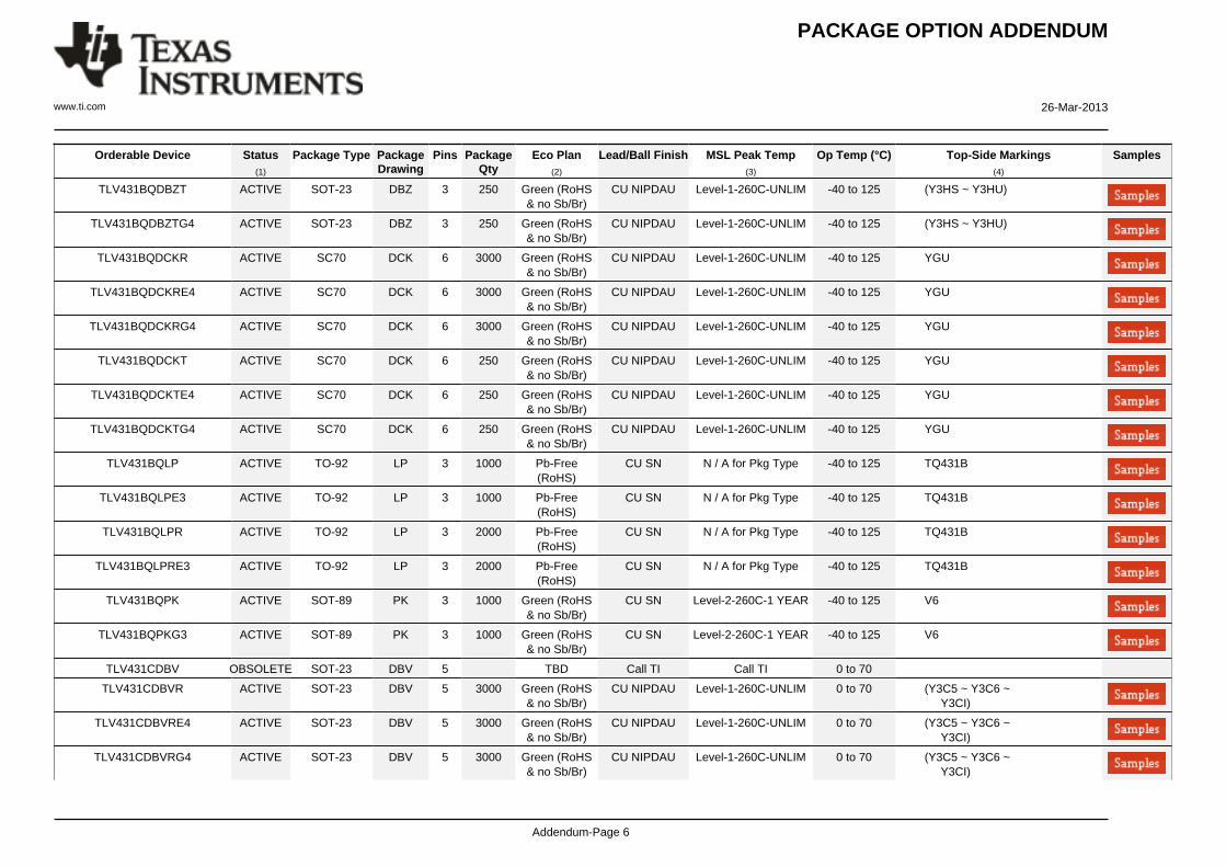
TLV431BQDBZT ACTIVE SOT-23 DBZ 3 250 Green (RoHS& no Sb/Br)
CU NIPDAU Level-1-260C-UNLIM -40 to 125 (Y3HS ~ Y3HU)
TLV431BQDBZTG4 ACTIVE SOT-23 DBZ 3 250 Green (RoHS& no Sb/Br)
CU NIPDAU Level-1-260C-UNLIM -40 to 125 (Y3HS ~ Y3HU)
TLV431BQDCKR ACTIVE SC70 DCK 6 3000 Green (RoHS& no Sb/Br)
CU NIPDAU Level-1-260C-UNLIM -40 to 125 YGU
TLV431BQDCKRE4 ACTIVE SC70 DCK 6 3000 Green (RoHS& no Sb/Br)
CU NIPDAU Level-1-260C-UNLIM -40 to 125 YGU
TLV431BQDCKRG4 ACTIVE SC70 DCK 6 3000 Green (RoHS& no Sb/Br)
CU NIPDAU Level-1-260C-UNLIM -40 to 125 YGU
TLV431BQDCKT ACTIVE SC70 DCK 6 250 Green (RoHS& no Sb/Br)
CU NIPDAU Level-1-260C-UNLIM -40 to 125 YGU
TLV431BQDCKTE4 ACTIVE SC70 DCK 6 250 Green (RoHS& no Sb/Br)
CU NIPDAU Level-1-260C-UNLIM -40 to 125 YGU
TLV431BQDCKTG4 ACTIVE SC70 DCK 6 250 Green (RoHS& no Sb/Br)
CU NIPDAU Level-1-260C-UNLIM -40 to 125 YGU
TLV431BQLP ACTIVE TO-92 LP 3 1000 Pb-Free(RoHS)
CU SN N / A for Pkg Type -40 to 125 TQ431B
TLV431BQLPE3 ACTIVE TO-92 LP 3 1000 Pb-Free(RoHS)
CU SN N / A for Pkg Type -40 to 125 TQ431B
TLV431BQLPR ACTIVE TO-92 LP 3 2000 Pb-Free(RoHS)
CU SN N / A for Pkg Type -40 to 125 TQ431B
TLV431BQLPRE3 ACTIVE TO-92 LP 3 2000 Pb-Free(RoHS)
CU SN N / A for Pkg Type -40 to 125 TQ431B
TLV431BQPK ACTIVE SOT-89 PK 3 1000 Green (RoHS& no Sb/Br)
CU SN Level-2-260C-1 YEAR -40 to 125 V6
TLV431BQPKG3 ACTIVE SOT-89 PK 3 1000 Green (RoHS& no Sb/Br)
CU SN Level-2-260C-1 YEAR -40 to 125 V6
TLV431CDBV OBSOLETE SOT-23 DBV 5 TBD Call TI Call TI 0 to 70
TLV431CDBVR ACTIVE SOT-23 DBV 5 3000 Green (RoHS& no Sb/Br)
CU NIPDAU Level-1-260C-UNLIM 0 to 70 (Y3C5 ~ Y3C6 ~ Y3CI)
TLV431CDBVRE4 ACTIVE SOT-23 DBV 5 3000 Green (RoHS& no Sb/Br)
CU NIPDAU Level-1-260C-UNLIM 0 to 70 (Y3C5 ~ Y3C6 ~ Y3CI)
TLV431CDBVRG4 ACTIVE SOT-23 DBV 5 3000 Green (RoHS& no Sb/Br)
CU NIPDAU Level-1-260C-UNLIM 0 to 70 (Y3C5 ~ Y3C6 ~ Y3CI)
PACKAGE OPTION ADDENDUM
www.ti.com 26-Mar-2013
Addendum-Page 7
Orderable Device Status(1)
Package Type PackageDrawing
Pins PackageQty
Eco Plan(2)
Lead/Ball Finish MSL Peak Temp(3)
Op Temp (°C) Top-Side Markings(4)
Samples
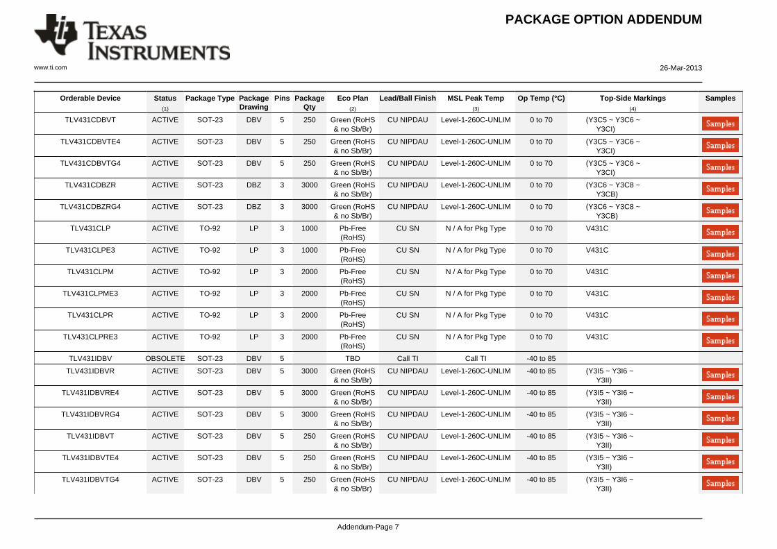
TLV431CDBVT ACTIVE SOT-23 DBV 5 250 Green (RoHS& no Sb/Br)
CU NIPDAU Level-1-260C-UNLIM 0 to 70 (Y3C5 ~ Y3C6 ~ Y3CI)
TLV431CDBVTE4 ACTIVE SOT-23 DBV 5 250 Green (RoHS& no Sb/Br)
CU NIPDAU Level-1-260C-UNLIM 0 to 70 (Y3C5 ~ Y3C6 ~ Y3CI)
TLV431CDBVTG4 ACTIVE SOT-23 DBV 5 250 Green (RoHS& no Sb/Br)
CU NIPDAU Level-1-260C-UNLIM 0 to 70 (Y3C5 ~ Y3C6 ~ Y3CI)
TLV431CDBZR ACTIVE SOT-23 DBZ 3 3000 Green (RoHS& no Sb/Br)
CU NIPDAU Level-1-260C-UNLIM 0 to 70 (Y3C6 ~ Y3C8 ~ Y3CB)
TLV431CDBZRG4 ACTIVE SOT-23 DBZ 3 3000 Green (RoHS& no Sb/Br)
CU NIPDAU Level-1-260C-UNLIM 0 to 70 (Y3C6 ~ Y3C8 ~ Y3CB)
TLV431CLP ACTIVE TO-92 LP 3 1000 Pb-Free(RoHS)
CU SN N / A for Pkg Type 0 to 70 V431C
TLV431CLPE3 ACTIVE TO-92 LP 3 1000 Pb-Free(RoHS)
CU SN N / A for Pkg Type 0 to 70 V431C
TLV431CLPM ACTIVE TO-92 LP 3 2000 Pb-Free(RoHS)
CU SN N / A for Pkg Type 0 to 70 V431C
TLV431CLPME3 ACTIVE TO-92 LP 3 2000 Pb-Free(RoHS)
CU SN N / A for Pkg Type 0 to 70 V431C
TLV431CLPR ACTIVE TO-92 LP 3 2000 Pb-Free(RoHS)
CU SN N / A for Pkg Type 0 to 70 V431C
TLV431CLPRE3 ACTIVE TO-92 LP 3 2000 Pb-Free(RoHS)
CU SN N / A for Pkg Type 0 to 70 V431C
TLV431IDBV OBSOLETE SOT-23 DBV 5 TBD Call TI Call TI -40 to 85
TLV431IDBVR ACTIVE SOT-23 DBV 5 3000 Green (RoHS& no Sb/Br)
CU NIPDAU Level-1-260C-UNLIM -40 to 85 (Y3I5 ~ Y3I6 ~ Y3II)
TLV431IDBVRE4 ACTIVE SOT-23 DBV 5 3000 Green (RoHS& no Sb/Br)
CU NIPDAU Level-1-260C-UNLIM -40 to 85 (Y3I5 ~ Y3I6 ~ Y3II)
TLV431IDBVRG4 ACTIVE SOT-23 DBV 5 3000 Green (RoHS& no Sb/Br)
CU NIPDAU Level-1-260C-UNLIM -40 to 85 (Y3I5 ~ Y3I6 ~ Y3II)
TLV431IDBVT ACTIVE SOT-23 DBV 5 250 Green (RoHS& no Sb/Br)
CU NIPDAU Level-1-260C-UNLIM -40 to 85 (Y3I5 ~ Y3I6 ~ Y3II)
TLV431IDBVTE4 ACTIVE SOT-23 DBV 5 250 Green (RoHS& no Sb/Br)
CU NIPDAU Level-1-260C-UNLIM -40 to 85 (Y3I5 ~ Y3I6 ~ Y3II)
TLV431IDBVTG4 ACTIVE SOT-23 DBV 5 250 Green (RoHS& no Sb/Br)
CU NIPDAU Level-1-260C-UNLIM -40 to 85 (Y3I5 ~ Y3I6 ~ Y3II)
PACKAGE OPTION ADDENDUM
www.ti.com 26-Mar-2013
Addendum-Page 8
Orderable Device Status(1)
Package Type PackageDrawing
Pins PackageQty
Eco Plan(2)
Lead/Ball Finish MSL Peak Temp(3)
Op Temp (°C) Top-Side Markings(4)
Samples
TLV431IDBZR ACTIVE SOT-23 DBZ 3 3000 Green (RoHS& no Sb/Br)
CU NIPDAU Level-1-260C-UNLIM -40 to 85 (Y3I6 ~ Y3IB)
TLV431IDBZRG4 ACTIVE SOT-23 DBZ 3 3000 Green (RoHS& no Sb/Br)
CU NIPDAU Level-1-260C-UNLIM -40 to 85 (Y3I6 ~ Y3IB)
TLV431ILP ACTIVE TO-92 LP 3 1000 Pb-Free(RoHS)
CU SN N / A for Pkg Type -40 to 85 V431I
TLV431ILPE3 ACTIVE TO-92 LP 3 1000 Pb-Free(RoHS)
CU SN N / A for Pkg Type -40 to 85 V431I
TLV431ILPR ACTIVE TO-92 LP 3 2000 Pb-Free(RoHS)
CU SN N / A for Pkg Type -40 to 85 V431I
TLV431ILPRE3 ACTIVE TO-92 LP 3 2000 Pb-Free(RoHS)
CU SN N / A for Pkg Type -40 to 85 V431I
TLV431QPK ACTIVE SOT-89 PK 3 1000 Green (RoHS& no Sb/Br)
CU SN Level-2-260C-1 YEAR -40 to 125 VB
TLV431QPKG3 ACTIVE SOT-89 PK 3 1000 Green (RoHS& no Sb/Br)
CU SN Level-2-260C-1 YEAR -40 to 125 VB
(1) The marketing status values are defined as follows:ACTIVE: Product device recommended for new designs.LIFEBUY: TI has announced that the device will be discontinued, and a lifetime-buy period is in effect.NRND: Not recommended for new designs. Device is in production to support existing customers, but TI does not recommend using this part in a new design.PREVIEW: Device has been announced but is not in production. Samples may or may not be available.OBSOLETE: TI has discontinued the production of the device.
(2) Eco Plan - The planned eco-friendly classification: Pb-Free (RoHS), Pb-Free (RoHS Exempt), or Green (RoHS & no Sb/Br) - please check http://www.ti.com/productcontent for the latest availabilityinformation and additional product content details.TBD: The Pb-Free/Green conversion plan has not been defined.Pb-Free (RoHS): TI's terms "Lead-Free" or "Pb-Free" mean semiconductor products that are compatible with the current RoHS requirements for all 6 substances, including the requirement thatlead not exceed 0.1% by weight in homogeneous materials. Where designed to be soldered at high temperatures, TI Pb-Free products are suitable for use in specified lead-free processes.Pb-Free (RoHS Exempt): This component has a RoHS exemption for either 1) lead-based flip-chip solder bumps used between the die and package, or 2) lead-based die adhesive used betweenthe die and leadframe. The component is otherwise considered Pb-Free (RoHS compatible) as defined above.Green (RoHS & no Sb/Br): TI defines "Green" to mean Pb-Free (RoHS compatible), and free of Bromine (Br) and Antimony (Sb) based flame retardants (Br or Sb do not exceed 0.1% by weightin homogeneous material)
(3) MSL, Peak Temp. -- The Moisture Sensitivity Level rating according to the JEDEC industry standard classifications, and peak solder temperature.
(4) Multiple Top-Side Markings will be inside parentheses. Only one Top-Side Marking contained in parentheses and separated by a "~" will appear on a device. If a line is indented then it is acontinuation of the previous line and the two combined represent the entire Top-Side Marking for that device.
PACKAGE OPTION ADDENDUM
www.ti.com 26-Mar-2013
Addendum-Page 9
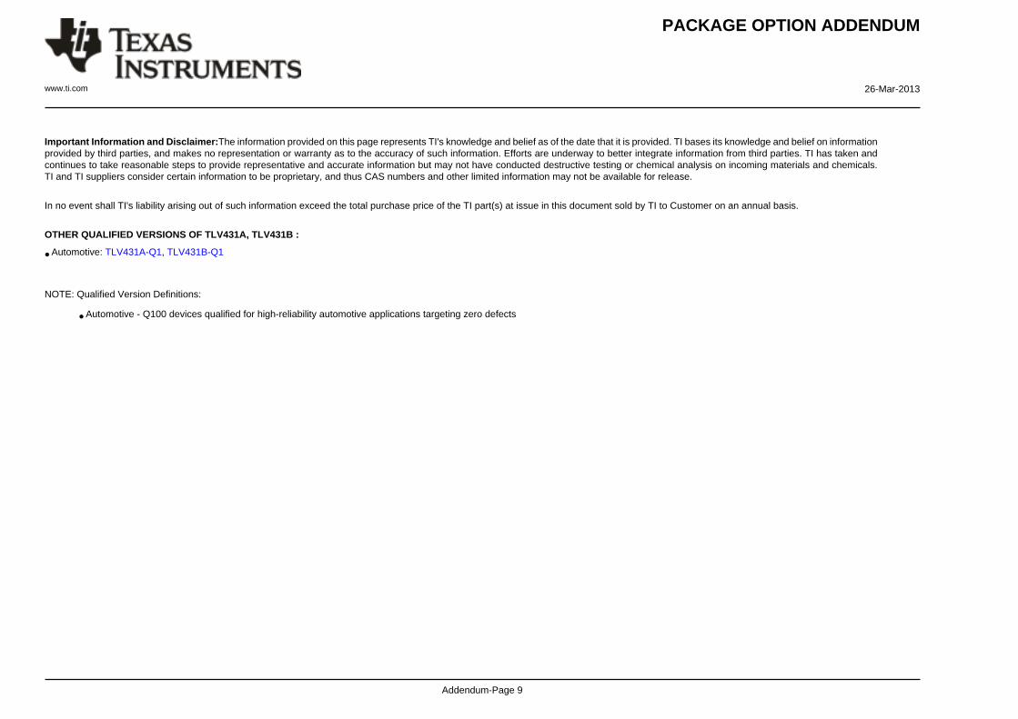
Important Information and Disclaimer:The information provided on this page represents TI's knowledge and belief as of the date that it is provided. TI bases its knowledge and belief on informationprovided by third parties, and makes no representation or warranty as to the accuracy of such information. Efforts are underway to better integrate information from third parties. TI has taken andcontinues to take reasonable steps to provide representative and accurate information but may not have conducted destructive testing or chemical analysis on incoming materials and chemicals.TI and TI suppliers consider certain information to be proprietary, and thus CAS numbers and other limited information may not be available for release.
In no event shall TI's liability arising out of such information exceed the total purchase price of the TI part(s) at issue in this document sold by TI to Customer on an annual basis.
OTHER QUALIFIED VERSIONS OF TLV431A, TLV431B :
• Automotive: TLV431A-Q1, TLV431B-Q1
NOTE: Qualified Version Definitions:
• Automotive - Q100 devices qualified for high-reliability automotive applications targeting zero defects
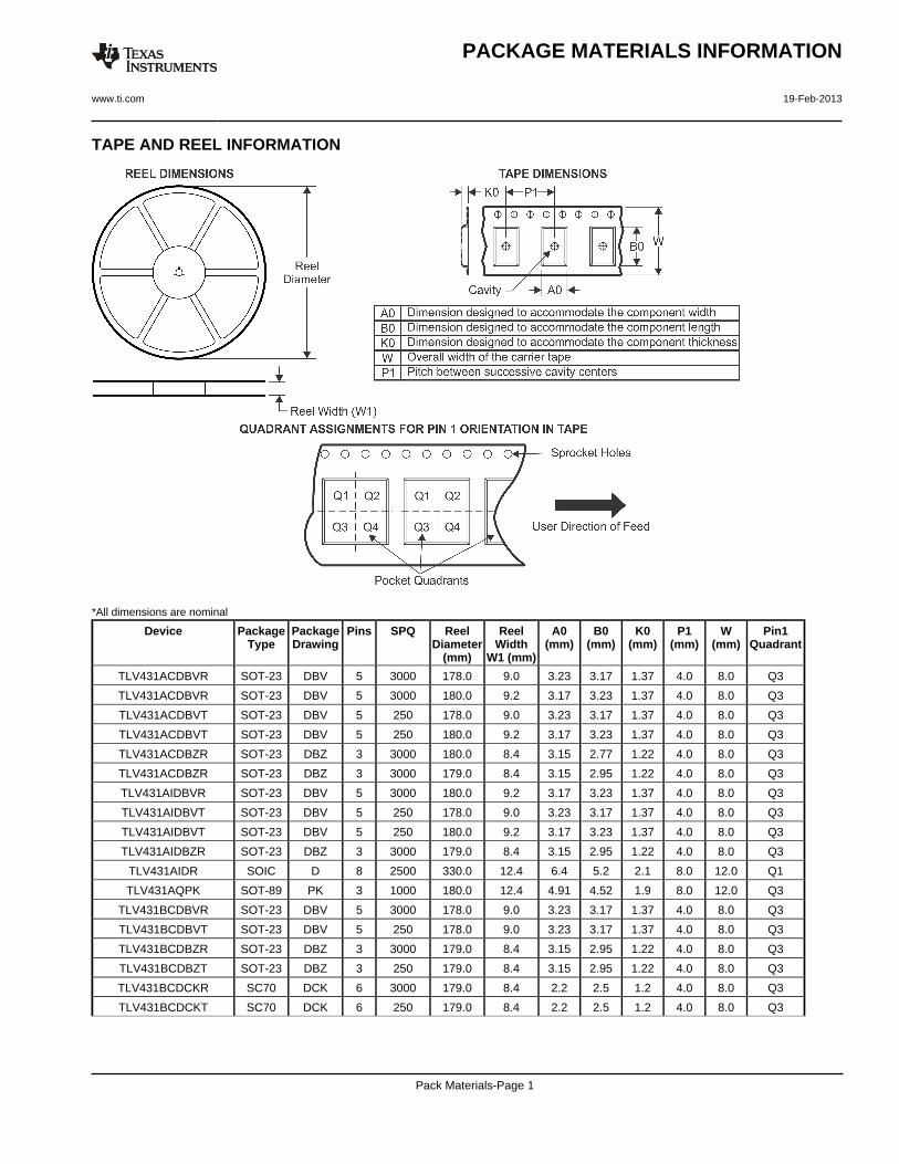
TAPE AND REEL INFORMATION
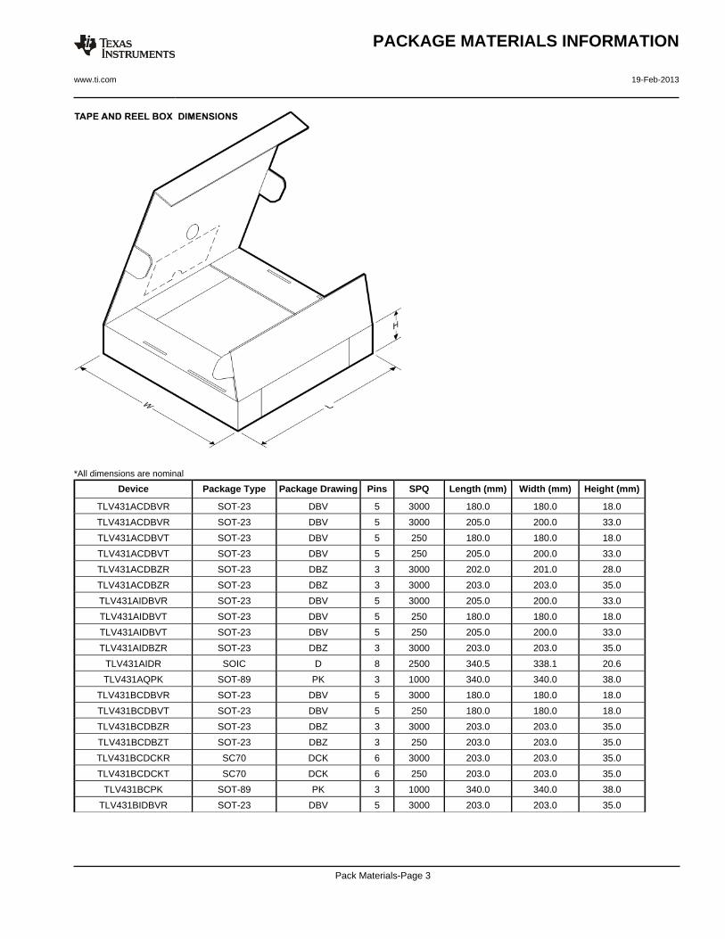
*All dimensions are nominal
Device PackageType
PackageDrawing
Pins SPQ ReelDiameter
(mm)
ReelWidth
W1 (mm)
A0(mm)
B0(mm)
K0(mm)
P1(mm)
W(mm)
Pin1Quadrant
TLV431ACDBVR SOT-23 DBV 5 3000 178.0 9.0 3.23 3.17 1.37 4.0 8.0 Q3
TLV431ACDBVR SOT-23 DBV 5 3000 180.0 9.2 3.17 3.23 1.37 4.0 8.0 Q3
TLV431ACDBVT SOT-23 DBV 5 250 178.0 9.0 3.23 3.17 1.37 4.0 8.0 Q3
TLV431ACDBVT SOT-23 DBV 5 250 180.0 9.2 3.17 3.23 1.37 4.0 8.0 Q3
TLV431ACDBZR SOT-23 DBZ 3 3000 180.0 8.4 3.15 2.77 1.22 4.0 8.0 Q3
TLV431ACDBZR SOT-23 DBZ 3 3000 179.0 8.4 3.15 2.95 1.22 4.0 8.0 Q3
TLV431AIDBVR SOT-23 DBV 5 3000 180.0 9.2 3.17 3.23 1.37 4.0 8.0 Q3
TLV431AIDBVT SOT-23 DBV 5 250 178.0 9.0 3.23 3.17 1.37 4.0 8.0 Q3
TLV431AIDBVT SOT-23 DBV 5 250 180.0 9.2 3.17 3.23 1.37 4.0 8.0 Q3
TLV431AIDBZR SOT-23 DBZ 3 3000 179.0 8.4 3.15 2.95 1.22 4.0 8.0 Q3
TLV431AIDR SOIC D 8 2500 330.0 12.4 6.4 5.2 2.1 8.0 12.0 Q1
TLV431AQPK SOT-89 PK 3 1000 180.0 12.4 4.91 4.52 1.9 8.0 12.0 Q3
TLV431BCDBVR SOT-23 DBV 5 3000 178.0 9.0 3.23 3.17 1.37 4.0 8.0 Q3
TLV431BCDBVT SOT-23 DBV 5 250 178.0 9.0 3.23 3.17 1.37 4.0 8.0 Q3
TLV431BCDBZR SOT-23 DBZ 3 3000 179.0 8.4 3.15 2.95 1.22 4.0 8.0 Q3
TLV431BCDBZT SOT-23 DBZ 3 250 179.0 8.4 3.15 2.95 1.22 4.0 8.0 Q3
TLV431BCDCKR SC70 DCK 6 3000 179.0 8.4 2.2 2.5 1.2 4.0 8.0 Q3
TLV431BCDCKT SC70 DCK 6 250 179.0 8.4 2.2 2.5 1.2 4.0 8.0 Q3
PACKAGE MATERIALS INFORMATION
www.ti.com 19-Feb-2013
Pack Materials-Page 1
Device PackageType
PackageDrawing
Pins SPQ ReelDiameter
(mm)
ReelWidth
W1 (mm)
A0(mm)
B0(mm)
K0(mm)
P1(mm)
W(mm)
Pin1Quadrant
TLV431BCPK SOT-89 PK 3 1000 180.0 12.4 4.91 4.52 1.9 8.0 12.0 Q3
TLV431BIDBVR SOT-23 DBV 5 3000 179.0 8.4 3.2 3.2 1.4 4.0 8.0 Q3
TLV431BIDBVT SOT-23 DBV 5 250 179.0 8.4 3.2 3.2 1.4 4.0 8.0 Q3
TLV431BIDBZR SOT-23 DBZ 3 3000 178.0 9.2 3.08 2.8 1.27 4.0 8.0 Q3
TLV431BIDBZT SOT-23 DBZ 3 250 179.0 8.4 3.15 2.95 1.22 4.0 8.0 Q3
TLV431BIDCKR SC70 DCK 6 3000 179.0 8.4 2.2 2.5 1.2 4.0 8.0 Q3
TLV431BIDCKT SC70 DCK 6 250 179.0 8.4 2.2 2.5 1.2 4.0 8.0 Q3
TLV431BIPK SOT-89 PK 3 1000 180.0 12.4 4.91 4.52 1.9 8.0 12.0 Q3
TLV431BQDBVR SOT-23 DBV 5 3000 179.0 8.4 3.2 3.2 1.4 4.0 8.0 Q3
TLV431BQDBVT SOT-23 DBV 5 250 179.0 8.4 3.2 3.2 1.4 4.0 8.0 Q3
TLV431BQDBZR SOT-23 DBZ 3 3000 179.0 8.4 3.15 2.95 1.22 4.0 8.0 Q3
TLV431BQDBZR SOT-23 DBZ 3 3000 180.0 8.4 3.15 2.77 1.22 4.0 8.0 Q3
TLV431BQDBZT SOT-23 DBZ 3 250 179.0 8.4 3.15 2.95 1.22 4.0 8.0 Q3
TLV431BQDCKR SC70 DCK 6 3000 179.0 8.4 2.2 2.5 1.2 4.0 8.0 Q3
TLV431BQDCKT SC70 DCK 6 250 179.0 8.4 2.2 2.5 1.2 4.0 8.0 Q3
TLV431BQPK SOT-89 PK 3 1000 180.0 12.4 4.91 4.52 1.9 8.0 12.0 Q3
TLV431CDBVR SOT-23 DBV 5 3000 178.0 9.0 3.23 3.17 1.37 4.0 8.0 Q3
TLV431CDBVT SOT-23 DBV 5 250 178.0 9.0 3.23 3.17 1.37 4.0 8.0 Q3
TLV431CDBZR SOT-23 DBZ 3 3000 179.0 8.4 3.15 2.95 1.22 4.0 8.0 Q3
TLV431IDBVR SOT-23 DBV 5 3000 178.0 9.0 3.23 3.17 1.37 4.0 8.0 Q3
TLV431IDBVT SOT-23 DBV 5 250 178.0 9.0 3.23 3.17 1.37 4.0 8.0 Q3
TLV431IDBZR SOT-23 DBZ 3 3000 179.0 8.4 3.15 2.95 1.22 4.0 8.0 Q3
TLV431QPK SOT-89 PK 3 1000 180.0 12.4 4.91 4.52 1.9 8.0 12.0 Q3
PACKAGE MATERIALS INFORMATION
www.ti.com 19-Feb-2013
Pack Materials-Page 2
*All dimensions are nominal
Device Package Type Package Drawing Pins SPQ Length (mm) Width (mm) Height (mm)
TLV431ACDBVR SOT-23 DBV 5 3000 180.0 180.0 18.0
TLV431ACDBVR SOT-23 DBV 5 3000 205.0 200.0 33.0
TLV431ACDBVT SOT-23 DBV 5 250 180.0 180.0 18.0
TLV431ACDBVT SOT-23 DBV 5 250 205.0 200.0 33.0
TLV431ACDBZR SOT-23 DBZ 3 3000 202.0 201.0 28.0
TLV431ACDBZR SOT-23 DBZ 3 3000 203.0 203.0 35.0
TLV431AIDBVR SOT-23 DBV 5 3000 205.0 200.0 33.0
TLV431AIDBVT SOT-23 DBV 5 250 180.0 180.0 18.0
TLV431AIDBVT SOT-23 DBV 5 250 205.0 200.0 33.0
TLV431AIDBZR SOT-23 DBZ 3 3000 203.0 203.0 35.0
TLV431AIDR SOIC D 8 2500 340.5 338.1 20.6
TLV431AQPK SOT-89 PK 3 1000 340.0 340.0 38.0
TLV431BCDBVR SOT-23 DBV 5 3000 180.0 180.0 18.0
TLV431BCDBVT SOT-23 DBV 5 250 180.0 180.0 18.0
TLV431BCDBZR SOT-23 DBZ 3 3000 203.0 203.0 35.0
TLV431BCDBZT SOT-23 DBZ 3 250 203.0 203.0 35.0
TLV431BCDCKR SC70 DCK 6 3000 203.0 203.0 35.0
TLV431BCDCKT SC70 DCK 6 250 203.0 203.0 35.0
TLV431BCPK SOT-89 PK 3 1000 340.0 340.0 38.0
TLV431BIDBVR SOT-23 DBV 5 3000 203.0 203.0 35.0
PACKAGE MATERIALS INFORMATION
www.ti.com 19-Feb-2013
Pack Materials-Page 3
Device Package Type Package Drawing Pins SPQ Length (mm) Width (mm) Height (mm)
TLV431BIDBVT SOT-23 DBV 5 250 203.0 203.0 35.0
TLV431BIDBZR SOT-23 DBZ 3 3000 180.0 180.0 18.0
TLV431BIDBZT SOT-23 DBZ 3 250 203.0 203.0 35.0
TLV431BIDCKR SC70 DCK 6 3000 203.0 203.0 35.0
TLV431BIDCKT SC70 DCK 6 250 203.0 203.0 35.0
TLV431BIPK SOT-89 PK 3 1000 340.0 340.0 38.0
TLV431BQDBVR SOT-23 DBV 5 3000 203.0 203.0 35.0
TLV431BQDBVT SOT-23 DBV 5 250 203.0 203.0 35.0
TLV431BQDBZR SOT-23 DBZ 3 3000 203.0 203.0 35.0
TLV431BQDBZR SOT-23 DBZ 3 3000 202.0 201.0 28.0
TLV431BQDBZT SOT-23 DBZ 3 250 203.0 203.0 35.0
TLV431BQDCKR SC70 DCK 6 3000 203.0 203.0 35.0
TLV431BQDCKT SC70 DCK 6 250 203.0 203.0 35.0
TLV431BQPK SOT-89 PK 3 1000 340.0 340.0 38.0
TLV431CDBVR SOT-23 DBV 5 3000 180.0 180.0 18.0
TLV431CDBVT SOT-23 DBV 5 250 180.0 180.0 18.0
TLV431CDBZR SOT-23 DBZ 3 3000 203.0 203.0 35.0
TLV431IDBVR SOT-23 DBV 5 3000 180.0 180.0 18.0
TLV431IDBVT SOT-23 DBV 5 250 180.0 180.0 18.0
TLV431IDBZR SOT-23 DBZ 3 3000 203.0 203.0 35.0
TLV431QPK SOT-89 PK 3 1000 340.0 340.0 38.0
PACKAGE MATERIALS INFORMATION
www.ti.com 19-Feb-2013
Pack Materials-Page 4
IMPORTANT NOTICE
Texas Instruments Incorporated and its subsidiaries (TI) reserve the right to make corrections, enhancements, improvements and otherchanges to its semiconductor products and services per JESD46, latest issue, and to discontinue any product or service per JESD48, latestissue. Buyers should obtain the latest relevant information before placing orders and should verify that such information is current andcomplete. All semiconductor products (also referred to herein as “components”) are sold subject to TI’s terms and conditions of salesupplied at the time of order acknowledgment.
TI warrants performance of its components to the specifications applicable at the time of sale, in accordance with the warranty in TI’s termsand conditions of sale of semiconductor products. Testing and other quality control techniques are used to the extent TI deems necessaryto support this warranty. Except where mandated by applicable law, testing of all parameters of each component is not necessarilyperformed.
TI assumes no liability for applications assistance or the design of Buyers’ products. Buyers are responsible for their products andapplications using TI components. To minimize the risks associated with Buyers’ products and applications, Buyers should provideadequate design and operating safeguards.
TI does not warrant or represent that any license, either express or implied, is granted under any patent right, copyright, mask work right, orother intellectual property right relating to any combination, machine, or process in which TI components or services are used. Informationpublished by TI regarding third-party products or services does not constitute a license to use such products or services or a warranty orendorsement thereof. Use of such information may require a license from a third party under the patents or other intellectual property of thethird party, or a license from TI under the patents or other intellectual property of TI.
Reproduction of significant portions of TI information in TI data books or data sheets is permissible only if reproduction is without alterationand is accompanied by all associated warranties, conditions, limitations, and notices. TI is not responsible or liable for such altereddocumentation. Information of third parties may be subject to additional restrictions.
Resale of TI components or services with statements different from or beyond the parameters stated by TI for that component or servicevoids all express and any implied warranties for the associated TI component or service and is an unfair and deceptive business practice.TI is not responsible or liable for any such statements.
Buyer acknowledges and agrees that it is solely responsible for compliance with all legal, regulatory and safety-related requirementsconcerning its products, and any use of TI components in its applications, notwithstanding any applications-related information or supportthat may be provided by TI. Buyer represents and agrees that it has all the necessary expertise to create and implement safeguards whichanticipate dangerous consequences of failures, monitor failures and their consequences, lessen the likelihood of failures that might causeharm and take appropriate remedial actions. Buyer will fully indemnify TI and its representatives against any damages arising out of the useof any TI components in safety-critical applications.
In some cases, TI components may be promoted specifically to facilitate safety-related applications. With such components, TI’s goal is tohelp enable customers to design and create their own end-product solutions that meet applicable functional safety standards andrequirements. Nonetheless, such components are subject to these terms.
No TI components are authorized for use in FDA Class III (or similar life-critical medical equipment) unless authorized officers of the partieshave executed a special agreement specifically governing such use.
Only those TI components which TI has specifically designated as military grade or “enhanced plastic” are designed and intended for use inmilitary/aerospace applications or environments. Buyer acknowledges and agrees that any military or aerospace use of TI componentswhich have not been so designated is solely at the Buyer's risk, and that Buyer is solely responsible for compliance with all legal andregulatory requirements in connection with such use.
TI has specifically designated certain components as meeting ISO/TS16949 requirements, mainly for automotive use. In any case of use ofnon-designated products, TI will not be responsible for any failure to meet ISO/TS16949.
Products Applications
Audio www.ti.com/audio Automotive and Transportation www.ti.com/automotive
Amplifiers amplifier.ti.com Communications and Telecom www.ti.com/communications
Data Converters dataconverter.ti.com Computers and Peripherals www.ti.com/computers
DLP® Products www.dlp.com Consumer Electronics www.ti.com/consumer-apps
DSP dsp.ti.com Energy and Lighting www.ti.com/energy
Clocks and Timers www.ti.com/clocks Industrial www.ti.com/industrial
Interface interface.ti.com Medical www.ti.com/medical
Logic logic.ti.com Security www.ti.com/security
Power Mgmt power.ti.com Space, Avionics and Defense www.ti.com/space-avionics-defense
Microcontrollers microcontroller.ti.com Video and Imaging www.ti.com/video
RFID www.ti-rfid.com
OMAP Applications Processors www.ti.com/omap TI E2E Community e2e.ti.com
Wireless Connectivity www.ti.com/wirelessconnectivity
Mailing Address: Texas Instruments, Post Office Box 655303, Dallas, Texas 75265Copyright © 2013, Texas Instruments Incorporated