Embed Size (px)
Citation preview
Product
Folder
Sample &Buy
Technical
Documents
Tools &
Software
Support &Community
LP2952-N, LP2952A, LP2953, LP2953ASNVS095F –MAY 2004–REVISED MARCH 2015
LP295x Adjustable Micropower Low-Dropout Voltage Regulators1 Features 3 Description
The LP2952 and LP2953 are micropower voltage1• 2.3-V to 30-V Input Voltage Range
regulators with very low quiescent current (130 μA• Output Voltage Adjusts from 1.23 V to 29 V typical at 1-mA load) and very low dropout voltage• 250-mA Output Current (typically 60 mV at light load and 470 mV at 250-mA
load current). They are ideally suited for battery-• Extremely Low Quiescent Currentpowered systems. Furthermore, the quiescent current• Low Dropout Voltage increases only slightly at dropout, which prolongs
• Extremely Tight Line and Load Regulation battery life.• Very Low Temperature Coefficient The LP2952 and LP2953 retain all the desirable• Current and Thermal Limiting characteristics of the LP2951, but offer increased
output current, additional features, and an improved• Reverse Battery-Input Protectionshutdown function.• 50-mA (Typical) Automatic Output DischargeThe automatic output discharge pulls the output down• LP2953 Versions Onlyquickly when the shutdown is activated.– Auxiliary Comparator Included With CMOS-
and TTL-Compatible Output Levels. Can Be The error flag goes low if the output voltage drops outof regulation.Used for Fault Detection, Low-Input Line
Detection, and so on. Reverse battery-input protection is provided.
The internal voltage reference is made available for2 Applicationsexternal use, providing a low temperature coefficient
• High-Efficiency Linear Regulator (20 ppm/°C) reference with very good line (0.03%)and load (0.04%) regulation.• Regulator With Undervoltage Shutdown
• Low-Dropout Battery-Powered RegulatorDevice Information(1)
• Snap-ON/Snap-OFF RegulatorPART NUMBER PACKAGE BODY SIZE (NOM)
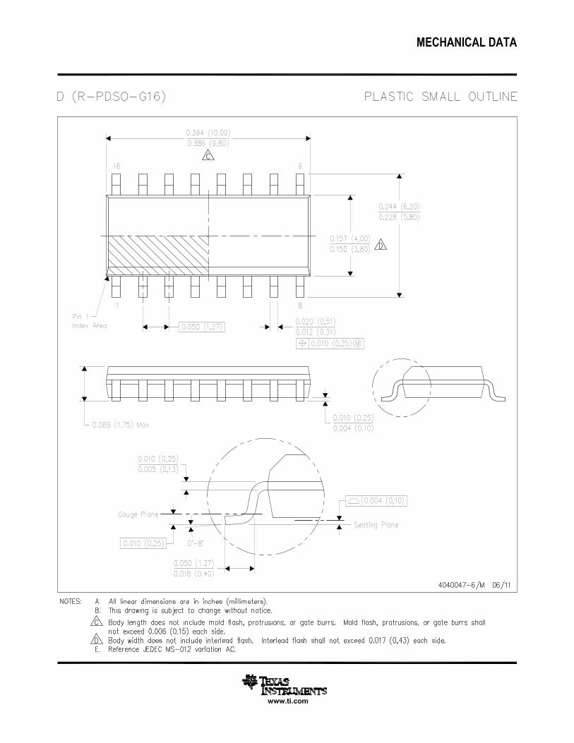
LP2952x SOIC (16) 9.90 mm × 3.91 mmSOIC (16) 9.90 mm × 3.91 mm
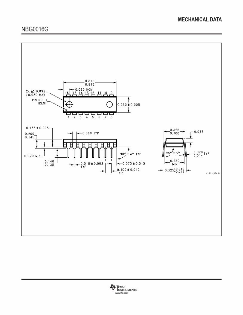
LP2953xPDIP (16) 21.755 mm × 6.35 mm
(1) For all available packages, see the orderable addendum atthe end of the data sheet.
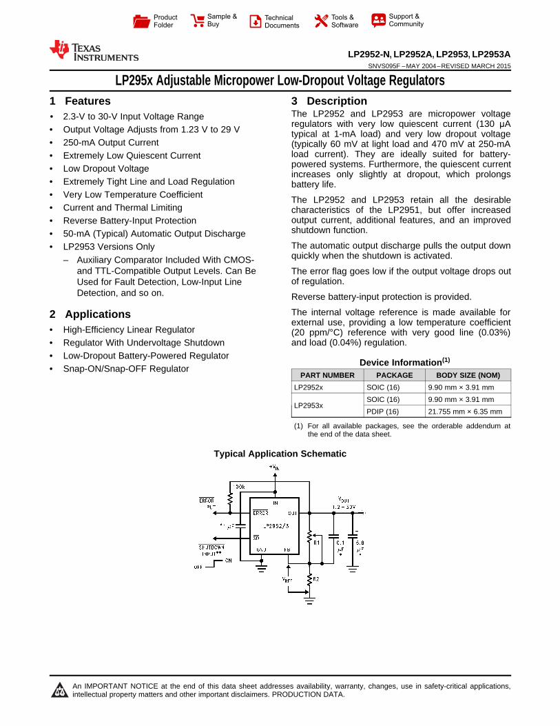
Typical Application Schematic
1
An IMPORTANT NOTICE at the end of this data sheet addresses availability, warranty, changes, use in safety-critical applications,intellectual property matters and other important disclaimers. PRODUCTION DATA.
LP2952-N, LP2952A, LP2953, LP2953ASNVS095F –MAY 2004–REVISED MARCH 2015 www.ti.com
Table of Contents7.3 Feature Description................................................. 151 Features .................................................................. 17.4 Device Functional Mode ......................................... 162 Applications ........................................................... 1
8 Application and Implementation ........................ 173 Description ............................................................. 18.1 Application Information............................................ 174 Revision History..................................................... 28.2 Typical Applications ................................................ 215 Pin Configuration and Functions ......................... 3
9 Power Supply Recommendations ...................... 306 Specifications......................................................... 410 Layout................................................................... 316.1 Absolute Maximum Ratings ...................................... 4
10.1 Layout Guidelines ................................................. 316.2 ESD Ratings.............................................................. 410.2 Layout Example .................................................... 316.3 Recommended Operating Conditions....................... 410.3 Power Dissipation: Heatsink Requirements6.4 Thermal Information .................................................. 5
(Industrial Temperature Range Devices) ................. 326.5 Electrical Characteristics: 3.3-V Versions ................. 511 Device and Documentation Support ................. 346.6 Electrical Characteristics: 5-V Versions .................... 5
11.1 Related Links ........................................................ 346.7 Electrical Characteristics: All Voltage Options.......... 611.2 Trademarks ........................................................... 346.8 Typical Characteristics .............................................. 911.3 Electrostatic Discharge Caution............................ 347 Detailed Description ............................................ 1411.4 Glossary ................................................................ 347.1 Overview ................................................................. 14
12 Mechanical, Packaging, and Orderable7.2 Functional Block Diagrams ..................................... 14 Information ........................................................... 34
4 Revision HistoryNOTE: Page numbers for previous revisions may differ from page numbers in the current version.
Changes from Revision E (December 2014) to Revision F Page
• Deleted "Assured" .................................................................................................................................................................. 1• Changed "Output Pulldown Crowbar" to "Automatic Output Discharge" ............................................................................... 1• Changed "internal crowbar" to "automatic output discharge"................................................................................................. 1• Added word "input" after "battery" in Features and Description............................................................................................. 1• Changed pin names for IN and OUT to match TI nomenclature; fix typos ............................................................................ 1• Changed max junc. temp from 125°C to 150°C .................................................................................................................... 4• Changed wording of footnote 12 ........................................................................................................................................... 8• Added second bullet for "LP2953 versions only" ................................................................................................................. 14• Added Automatic Output Dischange subsection ................................................................................................................. 16• Deleted sentence "To achieve the smallest form factor, the TO-92 package is selected.".................................................. 22• Changed "With an efficiency of 83.3% and a 250-mA maximum load, the internal power dissipation is 250 mW,
which corresponds to a 19.2°C junction temperature rise for the SOIC package." to "With a VIN – VOUT differential of1 V and a maximum load current of 250 mA the internal junction temperature (TJ) of the SOIC package will rise19.2° above the ambient temperature."................................................................................................................................ 22
• Deleted "Thermal Resistance for Various Copper Heatsinking Patterns" table ................................................................... 33
Changes from Revision D (September 2013) to Revision E Page
• Added Pin Configuration and Functions section, ESD Ratings table, Feature Description section, Device FunctionalModes, Application and Implementation section, Power Supply Recommendations section, Layout section, Deviceand Documentation Support section, and Mechanical, Packaging, and Orderable Information section; updatedThermal Information values; deleted obsolete LP2953AM references .................................................................................. 1
Changes from Revision C (March 2005) to Revision D Page
• Changed layout of National Data Sheet to TI format ........................................................................................................... 30
2 Submit Documentation Feedback Copyright © 2004–2015, Texas Instruments Incorporated
Product Folder Links: LP2952-N LP2952A LP2953 LP2953A
LP2952-N, LP2952A, LP2953, LP2953Awww.ti.com SNVS095F –MAY 2004–REVISED MARCH 2015
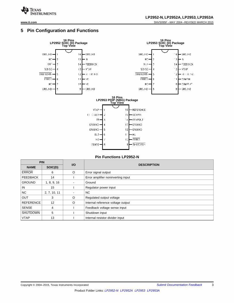
5 Pin Configuration and Functions
16 Pins 16 PinsLP2952 SOIC (D) Package LP2953 SOIC (D) Package
Top View Top View
16 PinsLP2953 PDIP (NBG) Package
Top View
Pin Functions LP2952-NPIN
I/O DESCRIPTIONNAME SOIC(D)
ERROR 6 O Error signal outputFEEDBACK 14 I Error amplifier noninverting inputGROUND 1, 8, 9, 16 - GroundIN 15 I Regulator power inputNC 2, 7, 10, 11 - NCOUT 3 O Regulated output voltageREFERENCE 12 O Internal reference voltage outputSENSE 4 I Feedback voltage sense inputSHUTDOWN 5 I Shutdown inputVTAP 13 I Internal resistor divider input
Copyright © 2004–2015, Texas Instruments Incorporated Submit Documentation Feedback 3
Product Folder Links: LP2952-N LP2952A LP2953 LP2953A
LP2952-N, LP2952A, LP2953, LP2953ASNVS095F –MAY 2004–REVISED MARCH 2015 www.ti.com
Pin Functions LP2953PIN
I/O DESCRIPTIONNAME SOIC(D) PDIP(NBG)
COMPIN 10 15 I Auxiliary comparator inputCOMPOUT 11 14 O Auxiliary comparator outputERROR 6 10 O Error signal outputFEEDBACK 14 2 I Error amplifier noninverting inputGROUND 1, 8, 9, 16 4, 5, 12, 13 - GroundIN 15 3 I Regulator power inputNC 2, 7 7, 11 - NCOUT 3 6 O Regulated output voltageREFERENCE 12 16 O Internal reference voltage outputSENSE 4 8 I Feedback voltage sense inputSHUTDOWN 5 9 I Shutdown inputVTAP 13 1 I Internal resistor divider input
6 Specifications
6.1 Absolute Maximum Ratingsover operating free-air temperature range (unless otherwise noted) (1)
MIN MAX UNITPower dissipation (2) Internally LimitedInput supply voltage −20 30 VFEEDBACK input voltage (3) −0.3 5 VComparator input voltage (4) −0.3 30 VSHUTDOWN input voltage (4) −0.3 30 VComparator output voltage (4) −0.3 30 VMaximum junction temperature 150 °CStorage temperature, Tstg −65 150 °C
(1) Stresses beyond those listed under Absolute Maximum Ratings may cause permanent damage to the device. These are stress ratingsonly, which do not imply functional operation of the device at these or any other conditions beyond those indicated under RecommendedOperating Conditions. Exposure to absolute-maximum-rated conditions for extended periods may affect device reliability.
(2) The maximum allowable power dissipation is a function of the maximum junction temperature, TJ(MAX), the junction-to-ambient thermalresistance, RθJA, and the ambient temperature, TA. The maximum allowable power dissipation at any ambient temperature is calculatedusing the equation for P(MAX): P(MAX) = (TJ(MAX) – TA) / RθJA.Exceeding the maximum allowable power dissipation will cause excessive die temperature, and the regulator will go into thermalshutdown. See Power Supply Recommendations for additional information on heatsinking and thermal resistance.
(3) When used in dual-supply systems where the regulator load is returned to a negative supply, the output voltage must be diode-clampedto ground.
(4) May exceed the input supply voltage.
6.2 ESD RatingsVALUE UNIT
Electrostatic Human body model (HBM), per ANSI/ESDA/JEDEC JS-001, all pins (1) ±2000V(ESD) Vdischarge
(1) JEDEC document JEP155 states that 500-V HBM allows safe manufacturing with a standard ESD control process.
6.3 Recommended Operating Conditionsover operating free-air temperature range (unless otherwise noted)
MIN MAX UNITOperating junction temperature −40 125 °CInput supply voltage 2.3 30 V
4 Submit Documentation Feedback Copyright © 2004–2015, Texas Instruments Incorporated
Product Folder Links: LP2952-N LP2952A LP2953 LP2953A
LP2952-N, LP2952A, LP2953, LP2953Awww.ti.com SNVS095F –MAY 2004–REVISED MARCH 2015
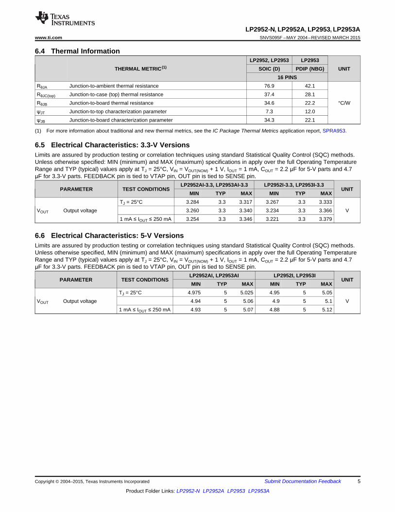
6.4 Thermal InformationLP2952, LP2953 LP2953
THERMAL METRIC (1) SOIC (D) PDIP (NBG) UNIT16 PINS
RθJA Junction-to-ambient thermal resistance 76.9 42.1RθJC(top) Junction-to-case (top) thermal resistance 37.4 28.1RθJB Junction-to-board thermal resistance 34.6 22.2 °C/WψJT Junction-to-top characterization parameter 7.3 12.0ψJB Junction-to-board characterization parameter 34.3 22.1
(1) For more information about traditional and new thermal metrics, see the IC Package Thermal Metrics application report, SPRA953.
6.5 Electrical Characteristics: 3.3-V VersionsLimits are assured by production testing or correlation techniques using standard Statistical Quality Control (SQC) methods.Unless otherwise specified: MIN (minimum) and MAX (maximum) specifications in apply over the full Operating TemperatureRange and TYP (typical) values apply at TJ = 25°C, VIN = VOUT(NOM) + 1 V, IOUT = 1 mA, COUT = 2.2 μF for 5-V parts and 4.7μF for 3.3-V parts. FEEDBACK pin is tied to VTAP pin, OUT pin is tied to SENSE pin.
LP2952AI-3.3, LP2953AI-3.3 LP2952I-3.3, LP2953I-3.3PARAMETER TEST CONDITIONS UNIT
MIN TYP MAX MIN TYP MAXTJ = 25°C 3.284 3.3 3.317 3.267 3.3 3.333
VOUT Output voltage 3.260 3.3 3.340 3.234 3.3 3.366 V1 mA ≤ IOUT ≤ 250 mA 3.254 3.3 3.346 3.221 3.3 3.379
6.6 Electrical Characteristics: 5-V VersionsLimits are assured by production testing or correlation techniques using standard Statistical Quality Control (SQC) methods.Unless otherwise specified, MIN (minimum) and MAX (maximum) specifications in apply over the full Operating TemperatureRange and TYP (typical) values apply at TJ = 25°C, VIN = VOUT(NOM) + 1 V, IOUT = 1 mA, COUT = 2.2 μF for 5-V parts and 4.7μF for 3.3-V parts. FEEDBACK pin is tied to VTAP pin, OUT pin is tied to SENSE pin.
LP2952AI, LP2953AI LP2952I, LP2953IPARAMETER TEST CONDITIONS UNIT
MIN TYP MAX MIN TYP MAXTJ = 25°C 4.975 5 5.025 4.95 5 5.05
VOUT Output voltage 4.94 5 5.06 4.9 5 5.1 V1 mA ≤ IOUT ≤ 250 mA 4.93 5 5.07 4.88 5 5.12
Copyright © 2004–2015, Texas Instruments Incorporated Submit Documentation Feedback 5
Product Folder Links: LP2952-N LP2952A LP2953 LP2953A
ûVOUT ûPD
ûVOUT ûV
ûVOUT ûV
ûVOUT ûT
LP2952-N, LP2952A, LP2953, LP2953ASNVS095F –MAY 2004–REVISED MARCH 2015 www.ti.com
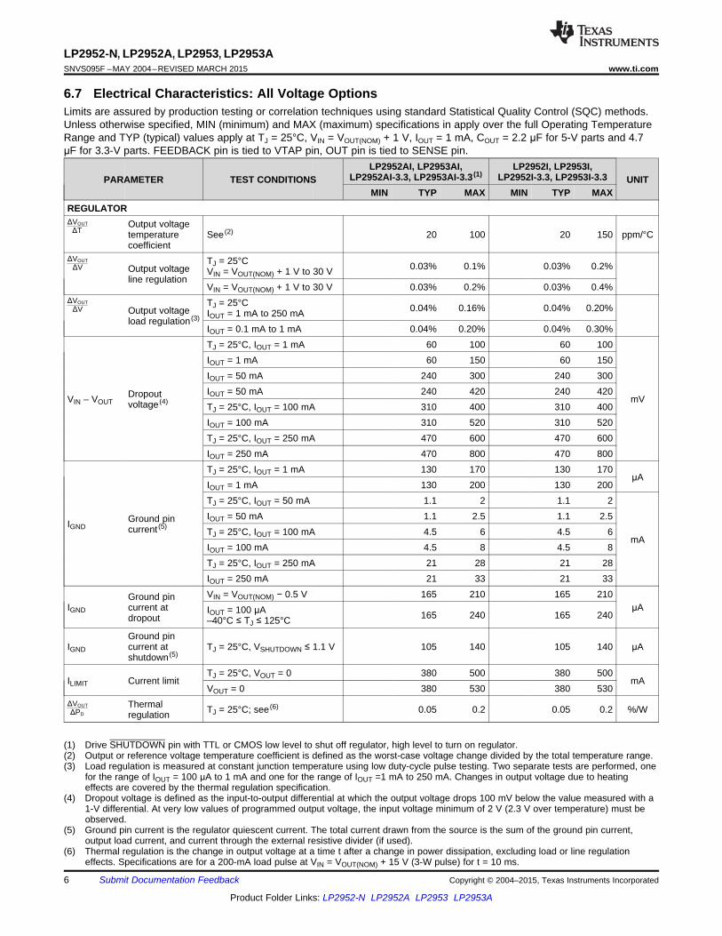
6.7 Electrical Characteristics: All Voltage OptionsLimits are assured by production testing or correlation techniques using standard Statistical Quality Control (SQC) methods.Unless otherwise specified, MIN (minimum) and MAX (maximum) specifications in apply over the full Operating TemperatureRange and TYP (typical) values apply at TJ = 25°C, VIN = VOUT(NOM) + 1 V, IOUT = 1 mA, COUT = 2.2 μF for 5-V parts and 4.7μF for 3.3-V parts. FEEDBACK pin is tied to VTAP pin, OUT pin is tied to SENSE pin.
LP2952AI, LP2953AI, LP2952I, LP2953I,LP2952AI-3.3, LP2953AI-3.3 (1) LP2952I-3.3, LP2953I-3.3PARAMETER TEST CONDITIONS UNIT
MIN TYP MAX MIN TYP MAXREGULATOR
Output voltagetemperature See (2) 20 100 20 150 ppm/°Ccoefficient
TJ = 25°C 0.03% 0.1% 0.03% 0.2%Output voltage VIN = VOUT(NOM) + 1 V to 30 Vline regulation
VIN = VOUT(NOM) + 1 V to 30 V 0.03% 0.2% 0.03% 0.4%TJ = 25°C 0.04% 0.16% 0.04% 0.20%Output voltage IOUT = 1 mA to 250 mA
load regulation (3)IOUT = 0.1 mA to 1 mA 0.04% 0.20% 0.04% 0.30%TJ = 25°C, IOUT = 1 mA 60 100 60 100IOUT = 1 mA 60 150 60 150IOUT = 50 mA 240 300 240 300IOUT = 50 mA 240 420 240 420DropoutVIN – VOUT mVvoltage (4) TJ = 25°C, IOUT = 100 mA 310 400 310 400IOUT = 100 mA 310 520 310 520TJ = 25°C, IOUT = 250 mA 470 600 470 600IOUT = 250 mA 470 800 470 800TJ = 25°C, IOUT = 1 mA 130 170 130 170
μAIOUT = 1 mA 130 200 130 200TJ = 25°C, IOUT = 50 mA 1.1 2 1.1 2IOUT = 50 mA 1.1 2.5 1.1 2.5Ground pinIGND current (5) TJ = 25°C, IOUT = 100 mA 4.5 6 4.5 6
mAIOUT = 100 mA 4.5 8 4.5 8TJ = 25°C, IOUT = 250 mA 21 28 21 28IOUT = 250 mA 21 33 21 33VIN = VOUT(NOM) − 0.5 V 165 210 165 210Ground pin
IGND current at μAIOUT = 100 μA 165 240 165 240dropout –40°C ≤ TJ ≤ 125°CGround pin
IGND current at TJ = 25°C, VSHUTDOWN ≤ 1.1 V 105 140 105 140 μAshutdown (5)
TJ = 25°C, VOUT = 0 380 500 380 500ILIMIT Current limit mA
VOUT = 0 380 530 380 530Thermal TJ = 25°C; see (6) 0.05 0.2 0.05 0.2 %/Wregulation
(1) Drive SHUTDOWN pin with TTL or CMOS low level to shut off regulator, high level to turn on regulator.(2) Output or reference voltage temperature coefficient is defined as the worst-case voltage change divided by the total temperature range.(3) Load regulation is measured at constant junction temperature using low duty-cycle pulse testing. Two separate tests are performed, one
for the range of IOUT = 100 μA to 1 mA and one for the range of IOUT =1 mA to 250 mA. Changes in output voltage due to heatingeffects are covered by the thermal regulation specification.
(4) Dropout voltage is defined as the input-to-output differential at which the output voltage drops 100 mV below the value measured with a1-V differential. At very low values of programmed output voltage, the input voltage minimum of 2 V (2.3 V over temperature) must beobserved.
(5) Ground pin current is the regulator quiescent current. The total current drawn from the source is the sum of the ground pin current,output load current, and current through the external resistive divider (if used).
(6) Thermal regulation is the change in output voltage at a time t after a change in power dissipation, excluding load or line regulationeffects. Specifications are for a 200-mA load pulse at VIN = VOUT(NOM) + 15 V (3-W pulse) for t = 10 ms.
6 Submit Documentation Feedback Copyright © 2004–2015, Texas Instruments Incorporated
Product Folder Links: LP2952-N LP2952A LP2953 LP2953A
LP2952-N, LP2952A, LP2953, LP2953Awww.ti.com SNVS095F –MAY 2004–REVISED MARCH 2015
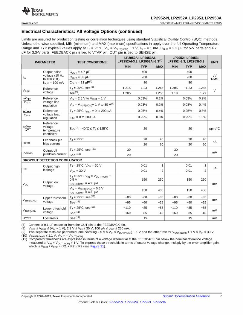
Electrical Characteristics: All Voltage Options (continued)Limits are assured by production testing or correlation techniques using standard Statistical Quality Control (SQC) methods.Unless otherwise specified, MIN (minimum) and MAX (maximum) specifications in apply over the full Operating TemperatureRange and TYP (typical) values apply at TJ = 25°C, VIN = VOUT(NOM) + 1 V, IOUT = 1 mA, COUT = 2.2 μF for 5-V parts and 4.7μF for 3.3-V parts. FEEDBACK pin is tied to VTAP pin, OUT pin is tied to SENSE pin.
LP2952AI, LP2953AI, LP2952I, LP2953I,LP2952AI-3.3, LP2953AI-3.3 (1) LP2952I-3.3, LP2953I-3.3PARAMETER TEST CONDITIONS UNIT
MIN TYP MAX MIN TYP MAXOutput noise COUT = 4.7 μF 400 400voltage (10 Hz μVCOUT = 33 μF 260 260en to 100 kHz) RMS
COUT = 33 μF (7) 80 80IOUT = 100 mATJ = 25°C, see (8) 1.215 1.23 1.245 1.205 1.23 1.255ReferenceVREF Vvoltage see (8), 1.205 1.255 1.19 1.27
Reference VIN = 2.5 V to VOUT + 1 V 0.03% 0.1% 0.03% 0.2%voltage line
VIN = VOUT(NOM)+ 1 V to 30 V (9) 0.03% 0.2% 0.03% 0.4%regulationReference TJ = 25°C, IREF = 0 to 200 μA 0.25% 0.4% 0.25% 0.8%voltage load
IREF = 0 to 200 μA 0.25% 0.6% 0.25% 1.0%regulationReferencevoltage See (2), –40°C ≤ TJ ≤ 125°C 20 20 ppm/°Ctemperaturecoefficient
TJ = 25°C 20 40 20 40Feedback pinIB(FB) nAbias current 20 60 20 60TJ = 25°C; see (10) 30 30Output offIO(SINK) mApulldown current See (10) 20 20
DROPOUT DETECTION COMPARATORTJ = 25°C, VOH = 30 V 0.01 1 0.01 1Output highIOH μAleakage VOH = 30 V 0.01 2 0.01 2TJ = 25°C, VIN = VOUT(NOM) −0.5 V 150 250 150 250
Output low IOUT(COMP) = 400 μAVOL mVvoltageVIN = VOUT(NOM) − 0.5 V 150 400 150 400IOUT(COMP) = 400 μATJ = 25°C, see (11) −80 −60 −35 −80 −60 −35Upper thresholdVTHR(MAX) mVvoltage See (11) −95 −60 −25 −95 −60 −25TJ = 25°C, see (11) −110 −85 −55 −110 −85 −55Lower thresholdVTHR(MIN) mVvoltage See (11) −160 −85 −40 −160 −85 −40
HYST Hysteresis See (11) 15 15 mV
(7) Connect a 0.1-μF capacitor from the OUT pin to the FEEDBACK pin.(8) VREF ≤ VOUT ≤ (VIN − 1 V), 2.3 V ≤ VIN ≤ 30 V, 100 μA ≤ IOUT ≤ 250 mA.(9) Two separate tests are performed, one covering 2.5 V ≤ VIN ≤ VOUT(NOM)) + 1 V and the other test for VOUT(NOM) + 1 V ≤ VIN ≤ 30 V.(10) VSHUTDOWN ≤ 1.1 V, VOUT = VOUT(NOM)(11) Comparator thresholds are expressed in terms of a voltage differential at the FEEDBACK pin below the nominal reference voltage
measured at VIN = VOUT(NOM) + 1 V. To express these thresholds in terms of output voltage change, multiply by the error amplifier gain,which is VOUT / VREF = (R1 + R2) / R2 (see Figure 31).
Copyright © 2004–2015, Texas Instruments Incorporated Submit Documentation Feedback 7
Product Folder Links: LP2952-N LP2952A LP2953 LP2953A
LP2952-N, LP2952A, LP2953, LP2953ASNVS095F –MAY 2004–REVISED MARCH 2015 www.ti.com
Electrical Characteristics: All Voltage Options (continued)Limits are assured by production testing or correlation techniques using standard Statistical Quality Control (SQC) methods.Unless otherwise specified, MIN (minimum) and MAX (maximum) specifications in apply over the full Operating TemperatureRange and TYP (typical) values apply at TJ = 25°C, VIN = VOUT(NOM) + 1 V, IOUT = 1 mA, COUT = 2.2 μF for 5-V parts and 4.7μF for 3.3-V parts. FEEDBACK pin is tied to VTAP pin, OUT pin is tied to SENSE pin.
LP2952AI, LP2953AI, LP2952I, LP2953I,LP2952AI-3.3, LP2953AI-3.3 (1) LP2952I-3.3, LP2953I-3.3PARAMETER TEST CONDITIONS UNIT
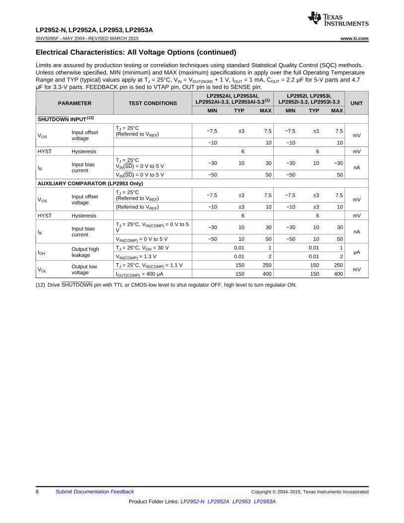
MIN TYP MAX MIN TYP MAXSHUTDOWN INPUT (12)
TJ = 25°C −7.5 ±3 7.5 −7.5 ±3 7.5Input offset (Referred to VREF)VOS mVvoltage−10 10 −10 10
HYST Hysteresis 6 6 mVTJ = 25°C −30 10 30 −30 10 −30Input bias VIN(SD) = 0 V to 5 VIB nAcurrentVIN(SD) = 0 V to 5 V −50 50 −50 50
AUXILIARY COMPARATOR (LP2953 Only)TJ = 25°C −7.5 ±3 7.5 −7.5 ±3 7.5Input offset (Referred to VREF)VOS mVvoltage(Referred to VREF) −10 ±3 10 −10 ±3 10
HYST Hysteresis 6 6 mVTJ = 25°C, VIN(COMP) = 0 V to 5 −30 10 30 −30 10 30Input bias VIB nAcurrentVIN(COMP) = 0 V to 5 V −50 10 50 −50 10 50TJ = 25°C, VOH = 30 V 0.01 1 0.01 1Output highIOH μAleakage VIN(COMP) = 1.3 V 0.01 2 0.01 2TJ = 25°C, VIN(COMP) = 1.1 V 150 250 150 250Output lowVOL mVvoltage IOUT(COMP) = 400 μA 150 400 150 400
(12) Drive SHUTDOWN pin with TTL or CMOS-low level to shut regulator OFF, high level to turn regulator ON.
8 Submit Documentation Feedback Copyright © 2004–2015, Texas Instruments Incorporated
Product Folder Links: LP2952-N LP2952A LP2953 LP2953A
LP2952-N, LP2952A, LP2953, LP2953Awww.ti.com SNVS095F –MAY 2004–REVISED MARCH 2015
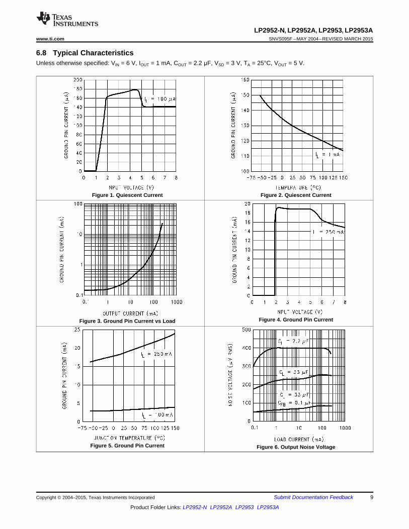
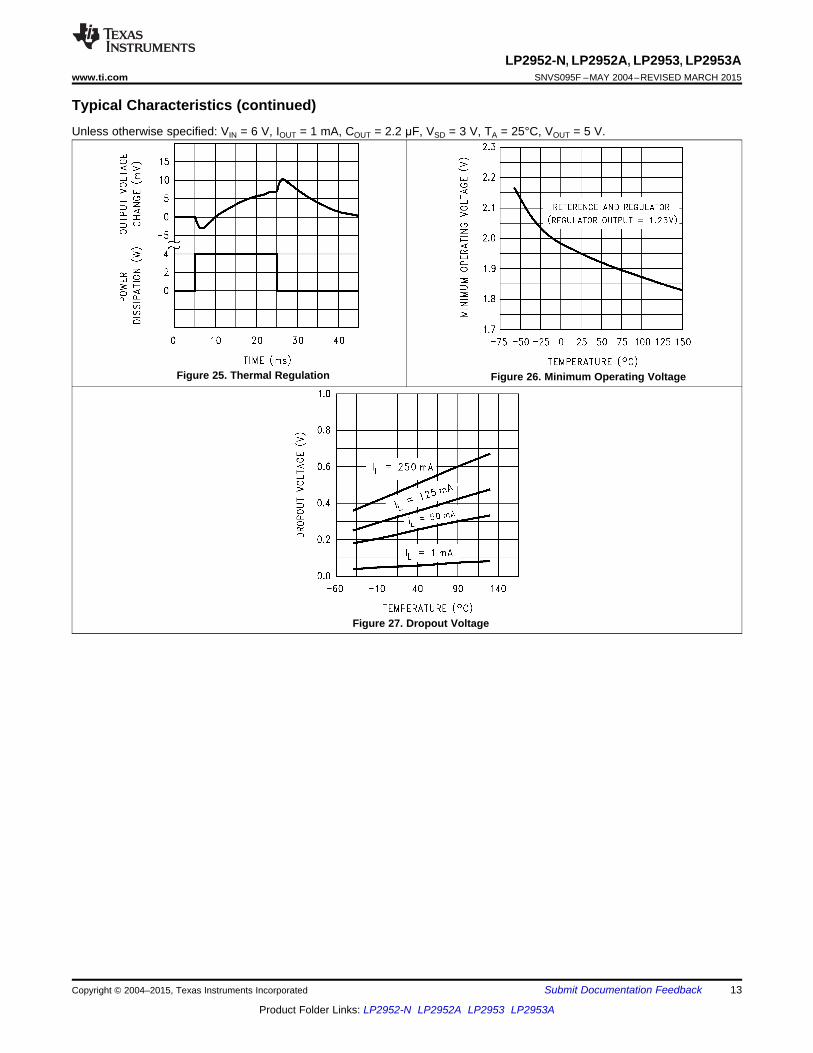
6.8 Typical CharacteristicsUnless otherwise specified: VIN = 6 V, IOUT = 1 mA, COUT = 2.2 μF, VSD = 3 V, TA = 25°C, VOUT = 5 V.
Figure 1. Quiescent Current Figure 2. Quiescent Current
Figure 4. Ground Pin CurrentFigure 3. Ground Pin Current vs Load
Figure 5. Ground Pin Current Figure 6. Output Noise Voltage
Copyright © 2004–2015, Texas Instruments Incorporated Submit Documentation Feedback 9
Product Folder Links: LP2952-N LP2952A LP2953 LP2953A
LP2952-N, LP2952A, LP2953, LP2953ASNVS095F –MAY 2004–REVISED MARCH 2015 www.ti.com
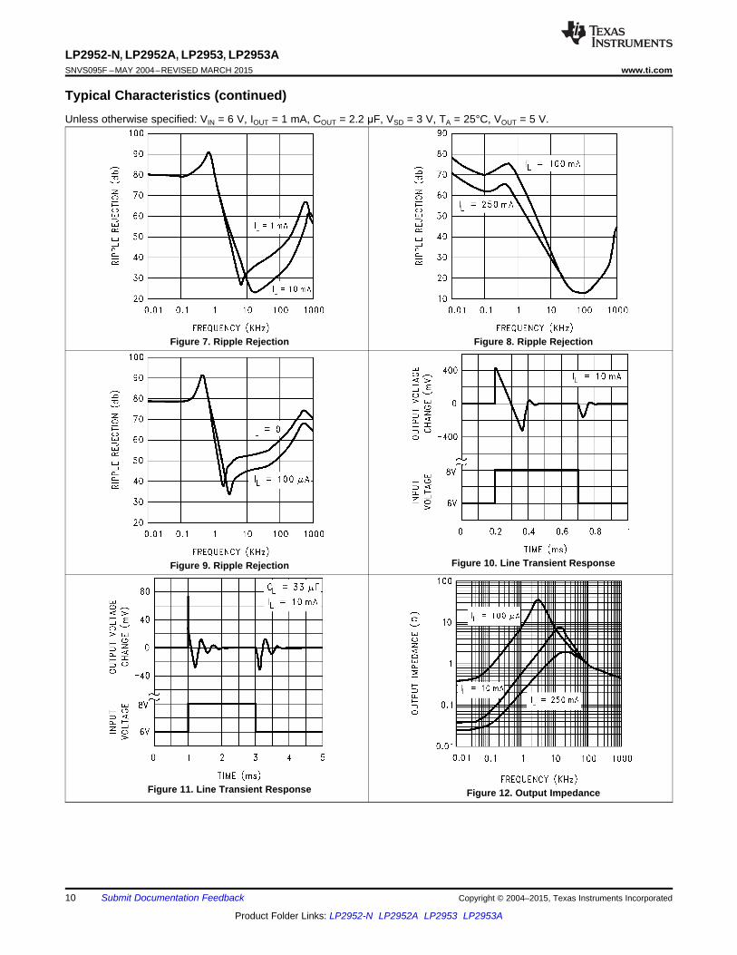
Typical Characteristics (continued)Unless otherwise specified: VIN = 6 V, IOUT = 1 mA, COUT = 2.2 μF, VSD = 3 V, TA = 25°C, VOUT = 5 V.
Figure 7. Ripple Rejection Figure 8. Ripple Rejection
Figure 10. Line Transient ResponseFigure 9. Ripple Rejection
Figure 11. Line Transient Response Figure 12. Output Impedance
10 Submit Documentation Feedback Copyright © 2004–2015, Texas Instruments Incorporated
Product Folder Links: LP2952-N LP2952A LP2953 LP2953A
LP2952-N, LP2952A, LP2953, LP2953Awww.ti.com SNVS095F –MAY 2004–REVISED MARCH 2015
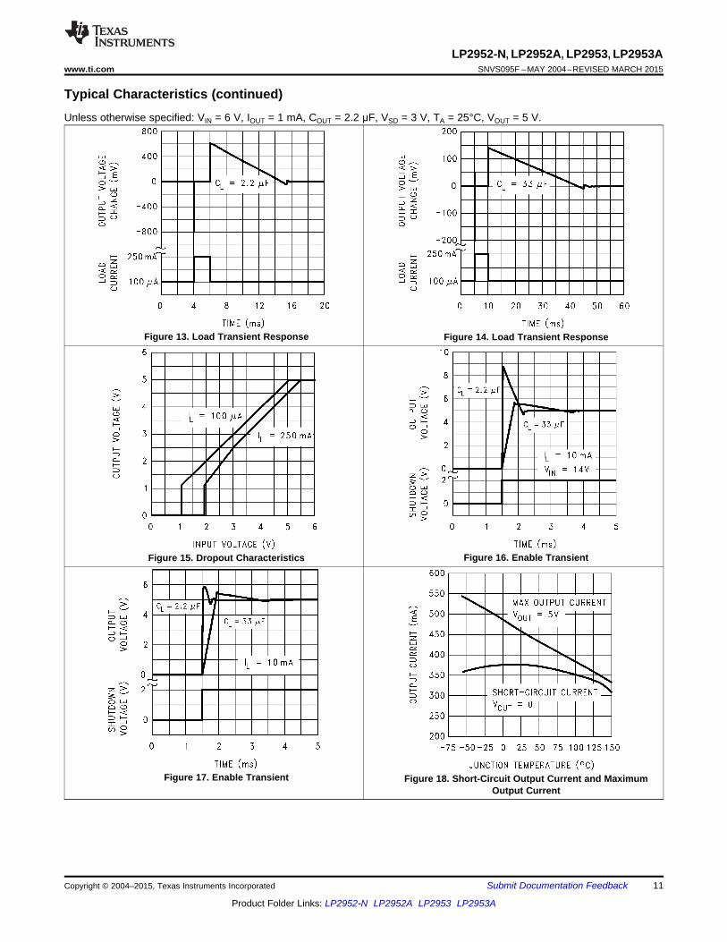
Typical Characteristics (continued)Unless otherwise specified: VIN = 6 V, IOUT = 1 mA, COUT = 2.2 μF, VSD = 3 V, TA = 25°C, VOUT = 5 V.
Figure 13. Load Transient Response Figure 14. Load Transient Response
Figure 16. Enable TransientFigure 15. Dropout Characteristics
Figure 17. Enable Transient Figure 18. Short-Circuit Output Current and MaximumOutput Current
Copyright © 2004–2015, Texas Instruments Incorporated Submit Documentation Feedback 11
Product Folder Links: LP2952-N LP2952A LP2953 LP2953A
LP2952-N, LP2952A, LP2953, LP2953ASNVS095F –MAY 2004–REVISED MARCH 2015 www.ti.com
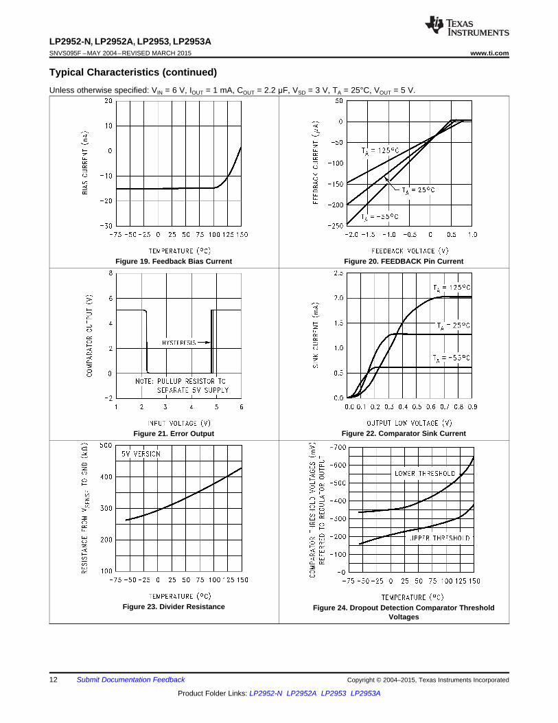
Typical Characteristics (continued)Unless otherwise specified: VIN = 6 V, IOUT = 1 mA, COUT = 2.2 μF, VSD = 3 V, TA = 25°C, VOUT = 5 V.
Figure 19. Feedback Bias Current Figure 20. FEEDBACK Pin Current
Figure 22. Comparator Sink CurrentFigure 21. Error Output
Figure 23. Divider Resistance Figure 24. Dropout Detection Comparator ThresholdVoltages
12 Submit Documentation Feedback Copyright © 2004–2015, Texas Instruments Incorporated
Product Folder Links: LP2952-N LP2952A LP2953 LP2953A
LP2952-N, LP2952A, LP2953, LP2953Awww.ti.com SNVS095F –MAY 2004–REVISED MARCH 2015
Typical Characteristics (continued)Unless otherwise specified: VIN = 6 V, IOUT = 1 mA, COUT = 2.2 μF, VSD = 3 V, TA = 25°C, VOUT = 5 V.
Figure 25. Thermal Regulation Figure 26. Minimum Operating Voltage
Figure 27. Dropout Voltage
Copyright © 2004–2015, Texas Instruments Incorporated Submit Documentation Feedback 13
Product Folder Links: LP2952-N LP2952A LP2953 LP2953A
LP2952-N, LP2952A, LP2953, LP2953ASNVS095F –MAY 2004–REVISED MARCH 2015 www.ti.com
7 Detailed Description
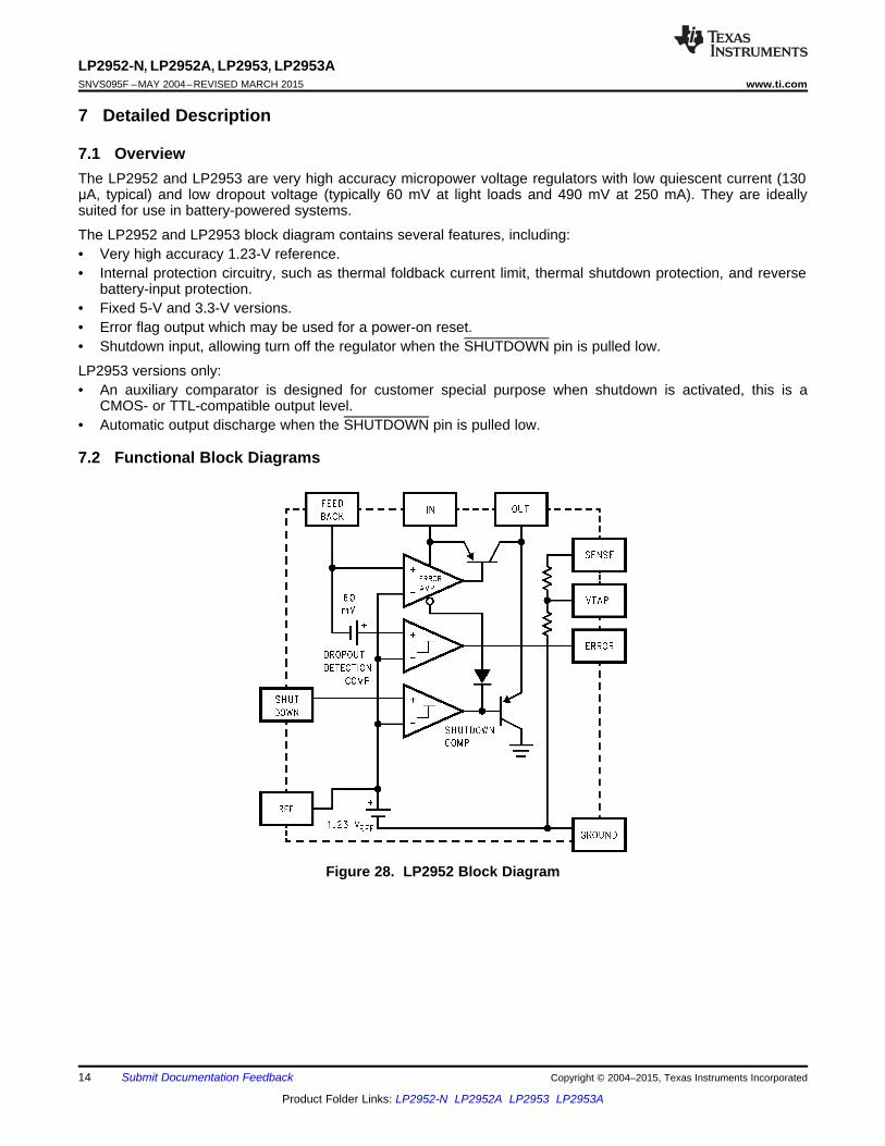
7.1 OverviewThe LP2952 and LP2953 are very high accuracy micropower voltage regulators with low quiescent current (130μA, typical) and low dropout voltage (typically 60 mV at light loads and 490 mV at 250 mA). They are ideallysuited for use in battery-powered systems.
The LP2952 and LP2953 block diagram contains several features, including:• Very high accuracy 1.23-V reference.• Internal protection circuitry, such as thermal foldback current limit, thermal shutdown protection, and reverse
battery-input protection.• Fixed 5-V and 3.3-V versions.• Error flag output which may be used for a power-on reset.• Shutdown input, allowing turn off the regulator when the SHUTDOWN pin is pulled low.
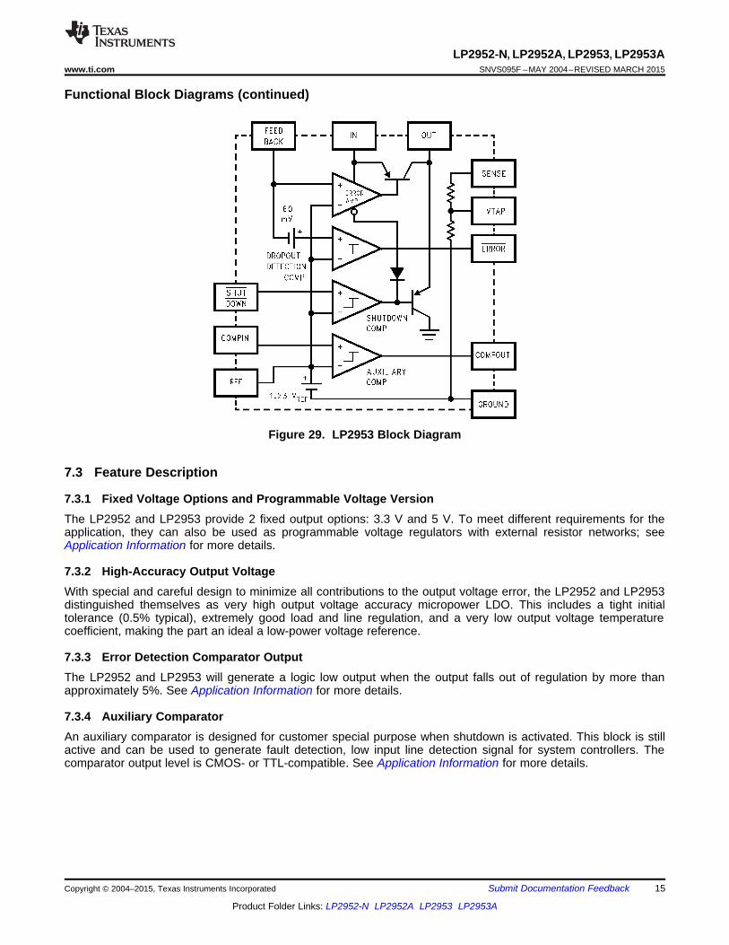
LP2953 versions only:• An auxiliary comparator is designed for customer special purpose when shutdown is activated, this is a
CMOS- or TTL-compatible output level.• Automatic output discharge when the SHUTDOWN pin is pulled low.
7.2 Functional Block Diagrams
Figure 28. LP2952 Block Diagram
14 Submit Documentation Feedback Copyright © 2004–2015, Texas Instruments Incorporated
Product Folder Links: LP2952-N LP2952A LP2953 LP2953A
LP2952-N, LP2952A, LP2953, LP2953Awww.ti.com SNVS095F –MAY 2004–REVISED MARCH 2015
Functional Block Diagrams (continued)
Figure 29. LP2953 Block Diagram
7.3 Feature Description
7.3.1 Fixed Voltage Options and Programmable Voltage VersionThe LP2952 and LP2953 provide 2 fixed output options: 3.3 V and 5 V. To meet different requirements for theapplication, they can also be used as programmable voltage regulators with external resistor networks; seeApplication Information for more details.
7.3.2 High-Accuracy Output VoltageWith special and careful design to minimize all contributions to the output voltage error, the LP2952 and LP2953distinguished themselves as very high output voltage accuracy micropower LDO. This includes a tight initialtolerance (0.5% typical), extremely good load and line regulation, and a very low output voltage temperaturecoefficient, making the part an ideal a low-power voltage reference.
7.3.3 Error Detection Comparator OutputThe LP2952 and LP2953 will generate a logic low output when the output falls out of regulation by more thanapproximately 5%. See Application Information for more details.
7.3.4 Auxiliary ComparatorAn auxiliary comparator is designed for customer special purpose when shutdown is activated. This block is stillactive and can be used to generate fault detection, low input line detection signal for system controllers. Thecomparator output level is CMOS- or TTL-compatible. See Application Information for more details.
Copyright © 2004–2015, Texas Instruments Incorporated Submit Documentation Feedback 15
Product Folder Links: LP2952-N LP2952A LP2953 LP2953A
LP2952-N, LP2952A, LP2953, LP2953ASNVS095F –MAY 2004–REVISED MARCH 2015 www.ti.com
Feature Description (continued)7.3.5 Short-Circuit Protection (Current Limit)The internal current limit circuit is used to protect the LDO against high-load current faults or shorting events. TheLDO is not designed to operate in a steady-state current limit. During a current-limit event, the LDO sourcesconstant current. Therefore, the output voltage falls when load impedance decreases. Note also that if a currentlimit occurs and the resulting output voltage is low, excessive power may be dissipated across the LDO resultingin a thermal shutdown of the output. A thermal foldback feature limits the short-circuit current to protect theregulator from damage under all load conditions. If the OUT pin is forced below 0 V before SHUTDOWN goeshigh and the load current required exceeds the thermal foldback current limit, the device may not start upcorrectly.
7.3.6 Thermal ProtectionThe device contains a thermal shutdown protection circuit to turn off the output current when excessive heat isdissipated in the LDO. The thermal time-constant of the semiconductor die is fairly short, and thus the outputcycles on and off at a high rate when thermal shutdown is reached until the power dissipation is reduced. Theinternal protection circuitry of the device is designed to protect against thermal overload conditions. The circuitryis not intended to replace a proper heatsink. Continuously running the device into thermal shutdown degrades itsreliability.
7.3.7 Automatic Output DischargeBoth LP2952 and LP2953 employ an internal 50-mA (typical) pulldown to discharge the output when theSHUTDOWN pin is low and the output is disabled.
7.4 Device Functional Mode
7.4.1 Shutdown ModeWhen pulling the SHUTDOWN pin to low level, the LP2952 and LP2953 will enter shutdown mode, and a verylow quiescent current is consumed. This function is designed for applications which needs a shutdown mode toeffectively enhance battery life cycle. When the SHUTDOWN pin is low the automatic output discharge circuitywill be active. See Application Information for more details.
7.4.2 Operation with 30 V ≥ VIN > VOUT(TARGET) + 1 VThe device operate if the input voltage is equal to, or exceeds, VOUT(TARGET) + 1 V, and SHUTDOWN is pulled tohigh level. At input voltages below the minimum VIN requirement, the devices do not operate correctly and outputvoltage may not reach target value.
16 Submit Documentation Feedback Copyright © 2004–2015, Texas Instruments Incorporated
Product Folder Links: LP2952-N LP2952A LP2953 LP2953A
LP2952-N, LP2952A, LP2953, LP2953Awww.ti.com SNVS095F –MAY 2004–REVISED MARCH 2015
8 Application and Implementation
NOTEInformation in the following applications sections is not part of the TI componentspecification, and TI does not warrant its accuracy or completeness. TI’s customers areresponsible for determining suitability of components for their purposes. Customers shouldvalidate and test their design implementation to confirm system functionality.
8.1 Application Information
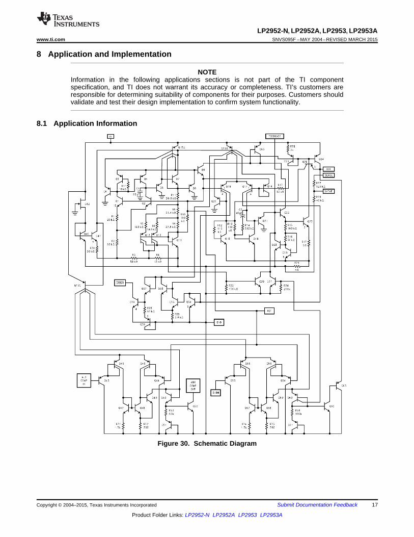
Figure 30. Schematic Diagram
Copyright © 2004–2015, Texas Instruments Incorporated Submit Documentation Feedback 17
Product Folder Links: LP2952-N LP2952A LP2953 LP2953A
LP2952-N, LP2952A, LP2953, LP2953ASNVS095F –MAY 2004–REVISED MARCH 2015 www.ti.com
Application Information (continued)8.1.1 External CapacitorsA 2.2-μF (or greater) capacitor is required between the OUT pin and ground to assure stability when the output isset to 5 V. Without this capacitor, the device will oscillate. Most types of tantalum or aluminum electrolyticcapacitors will work here. Film types will work, but are more expensive. Many aluminum electrolytic capacitorscontain electrolytes which freeze at −30°C, which requires the use of solid tantalum capacitors below −25°C. Theimportant parameters of the capacitor are an equivalent series resistance (ESR) of about 5 Ω or less and aresonant frequency above 500 kHz (the ESR may increase by a factor of 20 or 30 as the temperature is reducedfrom 25°C to −30°C). The value of this capacitor may be increased without limit.
At lower values of output current, less output capacitance is required for stability. The capacitor can be reducedto 0.68 μF for currents below 10 mA or 0.22 μF for currents below 1 mA.
Programming the output for voltages below 5 V runs the error amplifier at lower gains requiring more outputcapacitance for stability. At 3.3-V output, a minimum of 4.7 μF is required. For the worst-case condition of 1.23-Voutput and 250 mA of load current, a 6.8-μF (or larger) capacitor should be used.
A 1-μF capacitor should be placed from the IN pin to ground if there is more than 10 inches of wire between theIN pin and the ac filter capacitor or if a battery input is used.
Stray capacitance to the FEEDBACK pin can cause instability. This problem is most likely to appear when usinghigh-value external resistors to set the output voltage. Adding a 100-pF capacitor between the OUT andFEEDBACK pins and increasing the output capacitance to 6.8 μF (or greater) will cure the problem.
8.1.2 Minimum LoadWhen setting the output voltage using an external resistive divider, a minimum current of 1 μA is recommendedthrough the resistors to provide a minimum load.
It should be noted that a minimum load current is specified in several of the Electrical Characteristics: All VoltageOptions test conditions, so this value must be used to obtain correlation on these tested limits.
8.1.3 Programming the Output VoltageThe regulator may be pin-strapped for 5-V operation using its internal resistive divider by tying the OUTPUT andSENSE pins together and also tying the FEEDBACK and VTAP pins together.
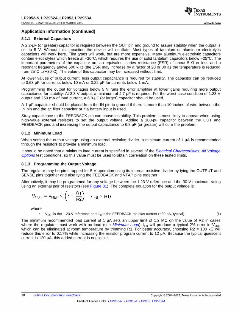
Alternatively, it may be programmed for any voltage between the 1.23-V reference and the 30-V maximum ratingusing an external pair of resistors (see Figure 31). The complete equation for the output voltage is:
where• VREF is the 1.23-V reference and IFB is the FEEDBACK pin bias current (−20 nA, typical). (1)
The minimum recommended load current of 1 μA sets an upper limit of 1.2 MΩ on the value of R2 in caseswhere the regulator must work with no load (see Minimum Load). IFB will produce a typical 2% error in VOUTwhich can be eliminated at room temperature by trimming R1. For better accuracy, choosing R2 = 100 kΩ willreduce this error to 0.17% while increasing the resistor program current to 12 μA. Because the typical quiescentcurrent is 120 μA, this added current is negligible.
18 Submit Documentation Feedback Copyright © 2004–2015, Texas Instruments Incorporated
Product Folder Links: LP2952-N LP2952A LP2953 LP2953A
LP2952-N, LP2952A, LP2953, LP2953Awww.ti.com SNVS095F –MAY 2004–REVISED MARCH 2015
Application Information (continued)
* See Power Supply Recommendations** Drive with TTL-low to shutdown
Figure 31. Adjustable Regulator
8.1.4 Dropout VoltageThe dropout voltage of the regulator is defined as the minimum input-to-output voltage differential required for theoutput voltage to stay within 100 mV of the output voltage measured with a 1-V differential. The dropout voltageis independent of the programmed output voltage.
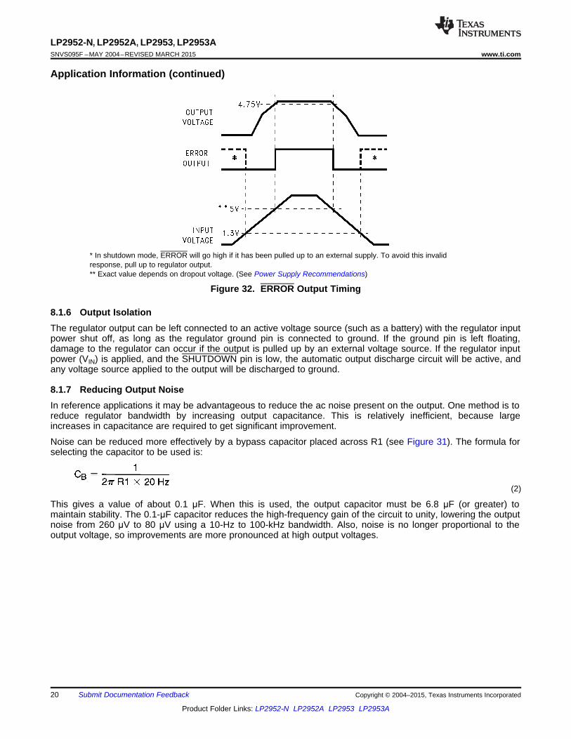
8.1.5 Dropout Detection ComparatorThis comparator produces a logic low whenever the output falls out of regulation by more than about 5%. Thisvalue results from the comparator built-in offset of 60 mV divided by the 1.23-V reference (see Functional BlockDiagrams). The 5% low trip level remains constant regardless of the programmed output voltage. An out-of-regulation condition can result from low input voltage, current limiting, or thermal limiting.
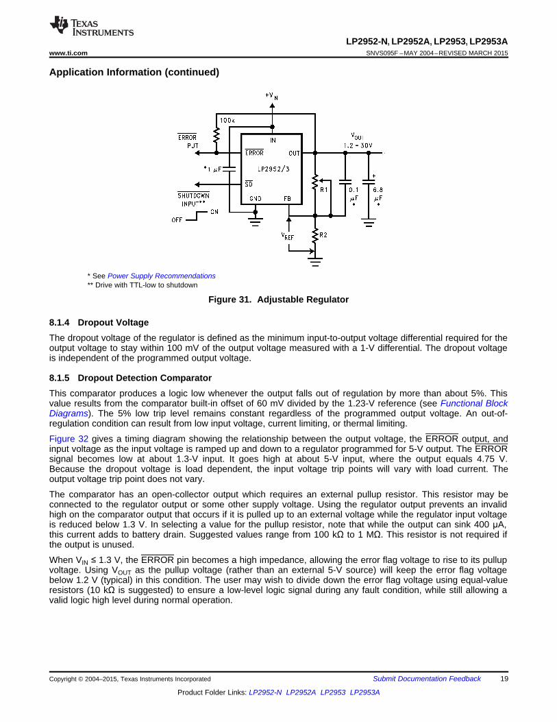
Figure 32 gives a timing diagram showing the relationship between the output voltage, the ERROR output, andinput voltage as the input voltage is ramped up and down to a regulator programmed for 5-V output. The ERRORsignal becomes low at about 1.3-V input. It goes high at about 5-V input, where the output equals 4.75 V.Because the dropout voltage is load dependent, the input voltage trip points will vary with load current. Theoutput voltage trip point does not vary.
The comparator has an open-collector output which requires an external pullup resistor. This resistor may beconnected to the regulator output or some other supply voltage. Using the regulator output prevents an invalidhigh on the comparator output that occurs if it is pulled up to an external voltage while the regulator input voltageis reduced below 1.3 V. In selecting a value for the pullup resistor, note that while the output can sink 400 μA,this current adds to battery drain. Suggested values range from 100 kΩ to 1 MΩ. This resistor is not required ifthe output is unused.
When VIN ≤ 1.3 V, the ERROR pin becomes a high impedance, allowing the error flag voltage to rise to its pullupvoltage. Using VOUT as the pullup voltage (rather than an external 5-V source) will keep the error flag voltagebelow 1.2 V (typical) in this condition. The user may wish to divide down the error flag voltage using equal-valueresistors (10 kΩ is suggested) to ensure a low-level logic signal during any fault condition, while still allowing avalid logic high level during normal operation.
Copyright © 2004–2015, Texas Instruments Incorporated Submit Documentation Feedback 19
Product Folder Links: LP2952-N LP2952A LP2953 LP2953A
LP2952-N, LP2952A, LP2953, LP2953ASNVS095F –MAY 2004–REVISED MARCH 2015 www.ti.com
Application Information (continued)
* In shutdown mode, ERROR will go high if it has been pulled up to an external supply. To avoid this invalidresponse, pull up to regulator output.** Exact value depends on dropout voltage. (See Power Supply Recommendations)
Figure 32. ERROR Output Timing
8.1.6 Output IsolationThe regulator output can be left connected to an active voltage source (such as a battery) with the regulator inputpower shut off, as long as the regulator ground pin is connected to ground. If the ground pin is left floating,damage to the regulator can occur if the output is pulled up by an external voltage source. If the regulator inputpower (VIN) is applied, and the SHUTDOWN pin is low, the automatic output discharge circuit will be active, andany voltage source applied to the output will be discharged to ground.
8.1.7 Reducing Output NoiseIn reference applications it may be advantageous to reduce the ac noise present on the output. One method is toreduce regulator bandwidth by increasing output capacitance. This is relatively inefficient, because largeincreases in capacitance are required to get significant improvement.
Noise can be reduced more effectively by a bypass capacitor placed across R1 (see Figure 31). The formula forselecting the capacitor to be used is:
(2)
This gives a value of about 0.1 μF. When this is used, the output capacitor must be 6.8 μF (or greater) tomaintain stability. The 0.1-μF capacitor reduces the high-frequency gain of the circuit to unity, lowering the outputnoise from 260 μV to 80 μV using a 10-Hz to 100-kHz bandwidth. Also, noise is no longer proportional to theoutput voltage, so improvements are more pronounced at high output voltages.
20 Submit Documentation Feedback Copyright © 2004–2015, Texas Instruments Incorporated
Product Folder Links: LP2952-N LP2952A LP2953 LP2953A
LP2952-N, LP2952A, LP2953, LP2953Awww.ti.com SNVS095F –MAY 2004–REVISED MARCH 2015
Application Information (continued)8.1.8 Auxiliary Comparator (LP2953 Only)The LP2953 contains an auxiliary comparator whose inverting input is connected to the 1.23-V reference. Theauxiliary comparator has an open-collector output whose electrical characteristics are similar to the dropoutdetection comparator. The noninverting input and output are brought out for external connections.
8.1.9 SHUTDOWN InputA logic-level signal will shut off the regulator output when a low (< 1.2 V) is applied to the SHUTDOWN input.
To prevent possible mis-operation, the SHUTDOWN input must be actively terminated. If the input is driven fromopen-collector logic, a pullup resistor (20 kΩ to 100 kΩ is recommended) should be connected from theSHUTDOWN input to the regulator input.
If the SHUTDOWN input is driven from a source that actively pulls high and low (like an op-amp), the pullupresistor is not required, but may be used.
If the shutdown function is not to be used, the cost of the pullup resistor can be saved by simply tying theSHUTDOWN input directly to the regulator input.
NOTEBecause the Absolute Maximum Ratings state that the SHUTDOWN input can not gomore than 0.3 V below ground, the reverse battery-input protection feature which protectsthe regulator input is sacrificed if the SHUTDOWN input is tied directly to the regulatorinput.
If reverse-battery input protection is required in an application, the pullup resistor between the SHUTDOWN inputand the regulator input must be used.
8.2 Typical Applications
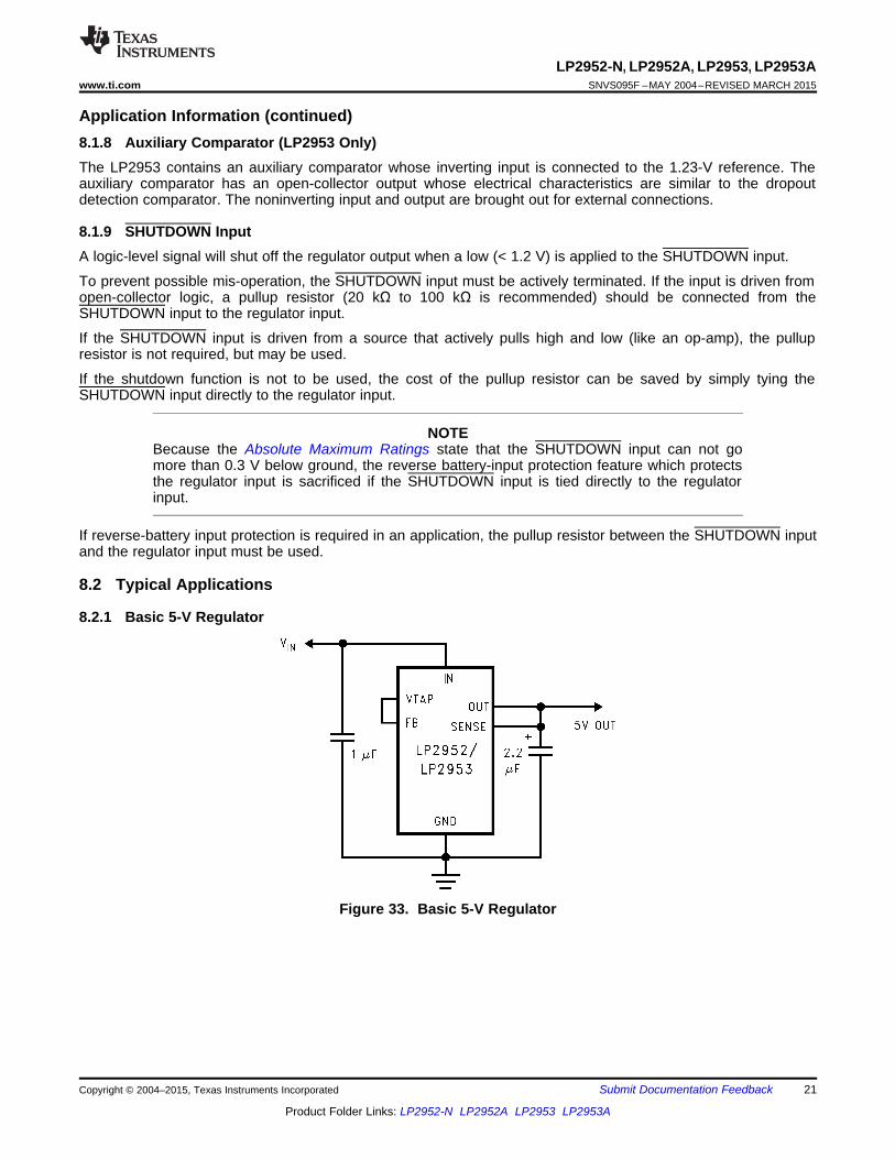
8.2.1 Basic 5-V Regulator
Figure 33. Basic 5-V Regulator
Copyright © 2004–2015, Texas Instruments Incorporated Submit Documentation Feedback 21
Product Folder Links: LP2952-N LP2952A LP2953 LP2953A
LP2952-N, LP2952A, LP2953, LP2953ASNVS095F –MAY 2004–REVISED MARCH 2015 www.ti.com
Typical Applications (continued)8.2.1.1 Design RequirementsFor this design example, use the parameters listed in Table 1 as the input parameters.
Table 1. Design ParametersDESIGN PARAMETER DESIGN REQUIREMENT
Input voltage 6 V, ±10%, provided by the DC-DC converter switching at 1 MHzOutput voltage 5 V, ±1%Output current 250 mA (maximum), 1 mA (minimum)
RMS noise, 10 Hz to 100 kHz 1 mV typicalPSRR at 1 kHz 50 dB typical
8.2.1.2 Detailed Design ProcedureAt 150-mA loading, the dropout of the LP2952 and LP2953 has 600-mV maximum dropout over temperature —thus, a 1500-mV headroom is sufficient for operation over both input and output voltage accuracy. The efficiencyof the LP2952 and LP2953 in this configuration is VOUT / VIN = 83.3%. Input and output capacitors are selected inaccordance with the External Capacitors section. Ceramic capacitances of 1 μF for the input and one 2.2-μFcapacitor for the output are selected. With an efficiency of 83.3% and a 250-mA maximum load, the internalpower dissipation is 250 mW, which corresponds to a 19.2°C junction temperature rise for the SOIC package.With a VIN – VOUT differential of 1 V and a maximum load current of 250 mA the internal junction temperature (TJ)of the SOIC package will rise 19.2°C above the ambient temperature. With an 85°C maximum ambienttemperature, the junction temperature is at 104.2°C. To minimize noise, a bypass capacitor of 100 pF is selectedbetween OUT and FEEDBACK pins.
8.2.1.3 Application Curves
Figure 34. Line Transient Response Figure 35. Load Transient Response
22 Submit Documentation Feedback Copyright © 2004–2015, Texas Instruments Incorporated
Product Folder Links: LP2952-N LP2952A LP2953 LP2953A
LP2952-N, LP2952A, LP2953, LP2953Awww.ti.com SNVS095F –MAY 2004–REVISED MARCH 2015
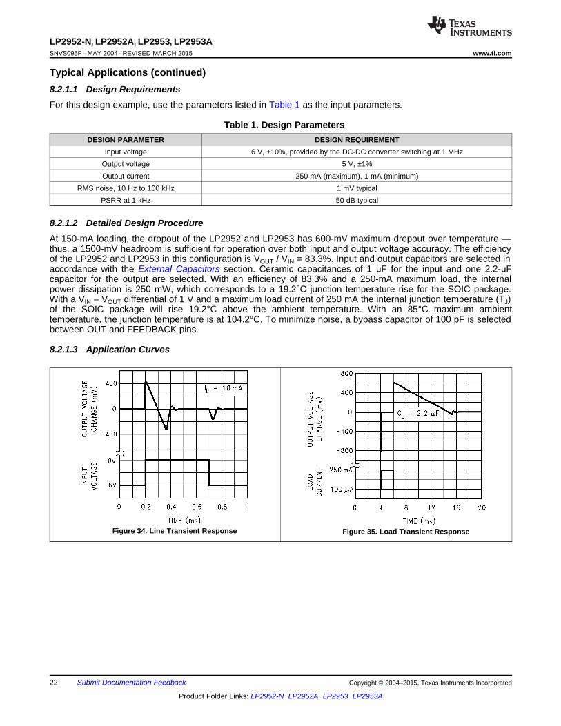
8.2.2 5-V Current Limiter with Load Fault IndicatorFigure 36 is the example circuit for 5-V current limiter with load fault indicator, it has the following features:• Output voltage equals +VIN minimum dropout voltage, which varies with output current. Current limits at a
maximum of 380 mA (typical).• Select R1 so that the comparator input voltage is 1.23 V at the output voltage which corresponds to the
desired fault current value.
Figure 36. 5-V Current Limiter With Load Fault Indicator
Copyright © 2004–2015, Texas Instruments Incorporated Submit Documentation Feedback 23
Product Folder Links: LP2952-N LP2952A LP2953 LP2953A
LP2952-N, LP2952A, LP2953, LP2953ASNVS095F –MAY 2004–REVISED MARCH 2015 www.ti.com
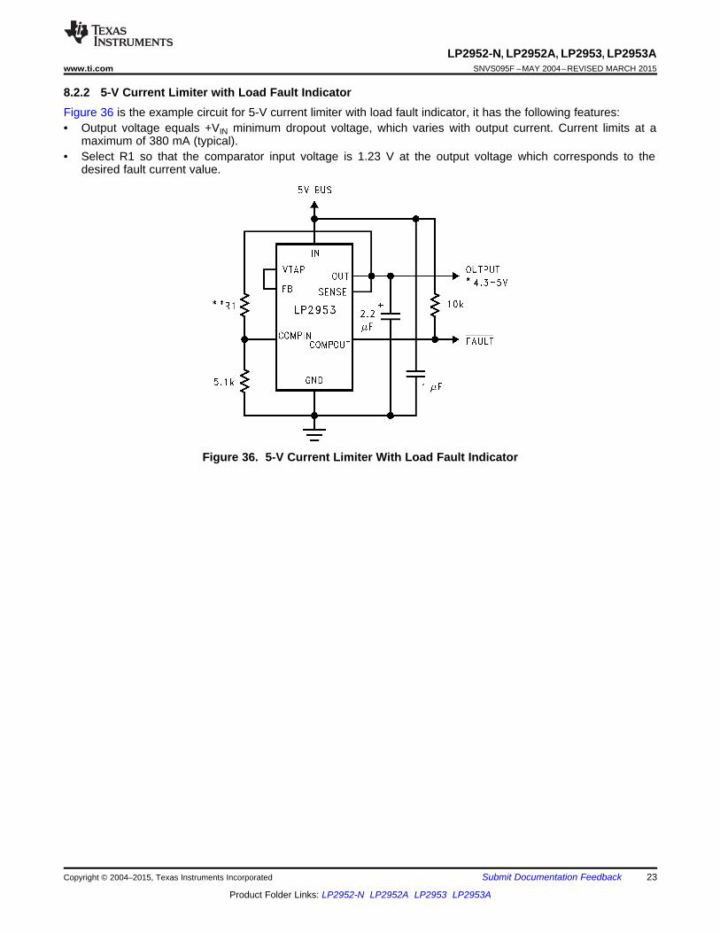
8.2.3 Low Temperature Coefficient Current SinkThe LP2952 or LP2953 can be used as a low drift current source as Figure 37 shows. By connecting VOUT toFEEDBACK, VOUT will be regulated at 1.235 V, and current consumption at R is IOUT = 1.23/R.
Figure 37. Low Temperature Coefficient Current Sink
24 Submit Documentation Feedback Copyright © 2004–2015, Texas Instruments Incorporated
Product Folder Links: LP2952-N LP2952A LP2953 LP2953A

LP2952-N, LP2952A, LP2953, LP2953Awww.ti.com SNVS095F –MAY 2004–REVISED MARCH 2015
8.2.4 5-V Regulator With Error Flags for Low Battery and Out of RegulationFigure 38 is the example circuit for 5-V regulator with error flags for low battery and out of regulation, it has thefollowing features:• Connect to logic or microprocessor control inputs.• LOW BATT flag warns the user that the battery has discharged down to about 5.8 V, giving the user time to
recharge the battery or power down some hardware with high power requirements. The output is still inregulation at this time.
• OUT OF REGULATION flag indicates when the battery is almost completely discharged, and can be used toinitiate a power-down sequence.
Figure 38. 5-V Regulator With Error Flags for Low Battery and Out of Regulation
Copyright © 2004–2015, Texas Instruments Incorporated Submit Documentation Feedback 25
Product Folder Links: LP2952-N LP2952A LP2953 LP2953A
LP2952-N, LP2952A, LP2953, LP2953ASNVS095F –MAY 2004–REVISED MARCH 2015 www.ti.com
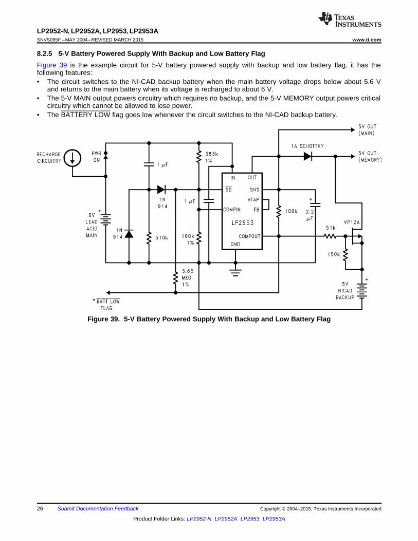
8.2.5 5-V Battery Powered Supply With Backup and Low Battery FlagFigure 39 is the example circuit for 5-V battery powered supply with backup and low battery flag, it has thefollowing features:• The circuit switches to the NI-CAD backup battery when the main battery voltage drops below about 5.6 V
and returns to the main battery when its voltage is recharged to about 6 V.• The 5-V MAIN output powers circuitry which requires no backup, and the 5-V MEMORY output powers critical
circuitry which cannot be allowed to lose power.• The BATTERY LOW flag goes low whenever the circuit switches to the NI-CAD backup battery.
Figure 39. 5-V Battery Powered Supply With Backup and Low Battery Flag
26 Submit Documentation Feedback Copyright © 2004–2015, Texas Instruments Incorporated
Product Folder Links: LP2952-N LP2952A LP2953 LP2953A
LP2952-N, LP2952A, LP2953, LP2953Awww.ti.com SNVS095F –MAY 2004–REVISED MARCH 2015
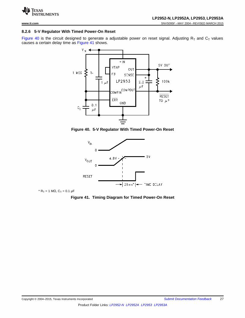
8.2.6 5-V Regulator With Timed Power-On ResetFigure 40 is the circuit designed to generate a adjustable power on reset signal. Adjusting RT and CT valuescauses a certain delay time as Figure 41 shows.
Figure 40. 5-V Regulator With Timed Power-On Reset
* RT = 1 MΩ, CT = 0.1 μF
Figure 41. Timing Diagram for Timed Power-On Reset
Copyright © 2004–2015, Texas Instruments Incorporated Submit Documentation Feedback 27
Product Folder Links: LP2952-N LP2952A LP2953 LP2953A
LP2952-N, LP2952A, LP2953, LP2953ASNVS095F –MAY 2004–REVISED MARCH 2015 www.ti.com
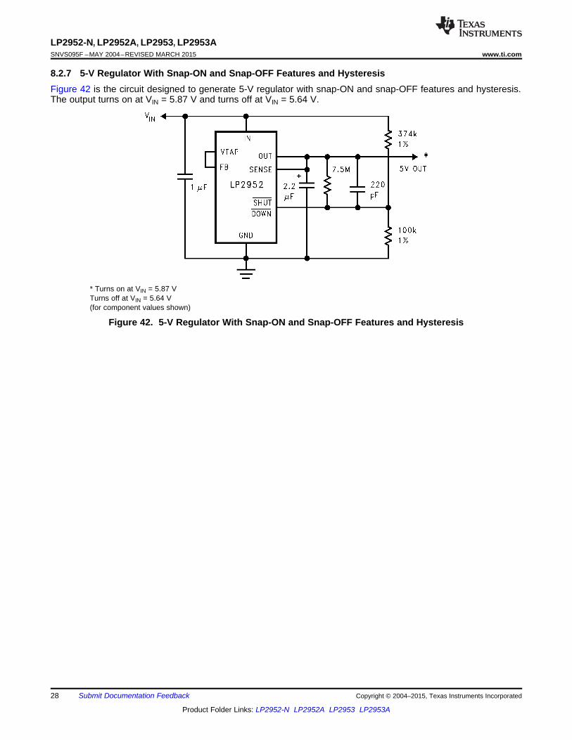
8.2.7 5-V Regulator With Snap-ON and Snap-OFF Features and HysteresisFigure 42 is the circuit designed to generate 5-V regulator with snap-ON and snap-OFF features and hysteresis.The output turns on at VIN = 5.87 V and turns off at VIN = 5.64 V.
* Turns on at VIN = 5.87 VTurns off at VIN = 5.64 V(for component values shown)
Figure 42. 5-V Regulator With Snap-ON and Snap-OFF Features and Hysteresis
28 Submit Documentation Feedback Copyright © 2004–2015, Texas Instruments Incorporated
Product Folder Links: LP2952-N LP2952A LP2953 LP2953A
LP2952-N, LP2952A, LP2953, LP2953Awww.ti.com SNVS095F –MAY 2004–REVISED MARCH 2015
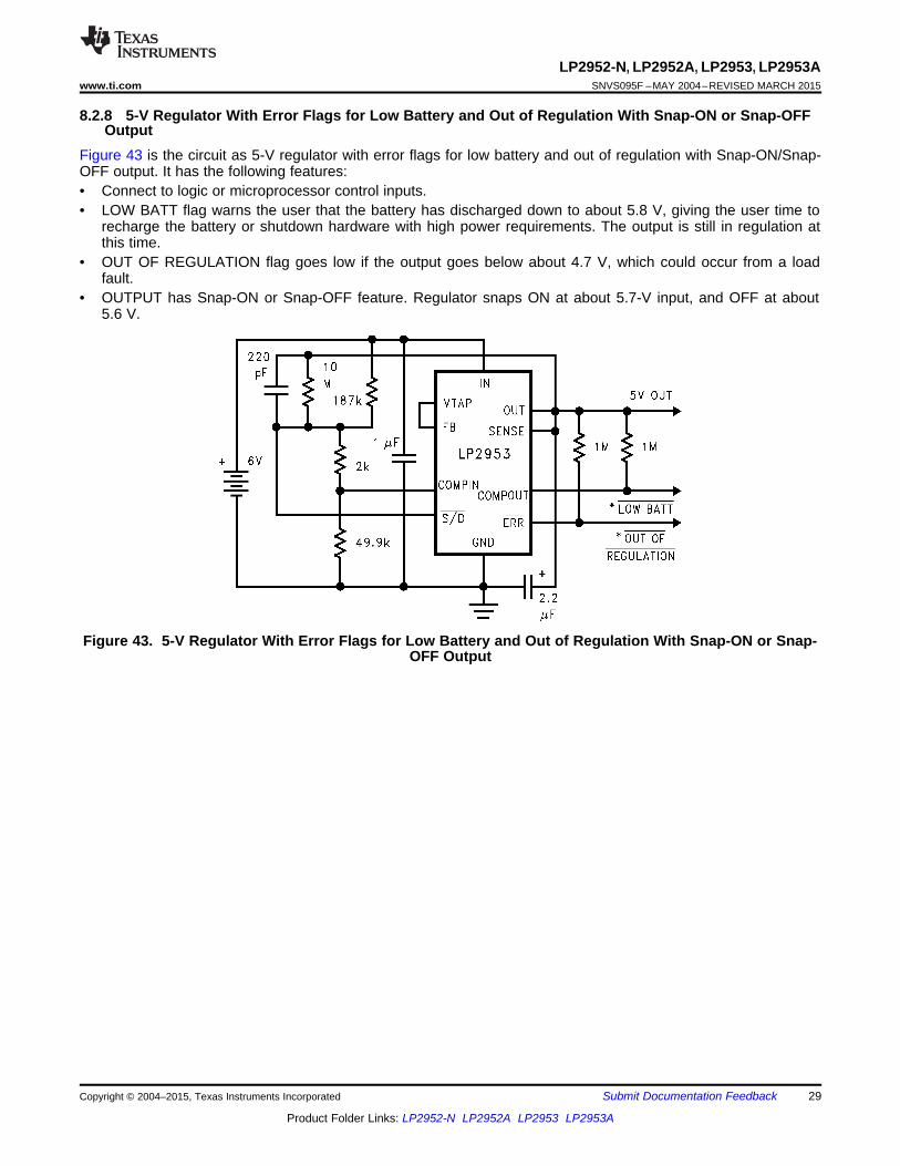
8.2.8 5-V Regulator With Error Flags for Low Battery and Out of Regulation With Snap-ON or Snap-OFFOutput
Figure 43 is the circuit as 5-V regulator with error flags for low battery and out of regulation with Snap-ON/Snap-OFF output. It has the following features:• Connect to logic or microprocessor control inputs.• LOW BATT flag warns the user that the battery has discharged down to about 5.8 V, giving the user time to
recharge the battery or shutdown hardware with high power requirements. The output is still in regulation atthis time.
• OUT OF REGULATION flag goes low if the output goes below about 4.7 V, which could occur from a loadfault.
• OUTPUT has Snap-ON or Snap-OFF feature. Regulator snaps ON at about 5.7-V input, and OFF at about5.6 V.
Figure 43. 5-V Regulator With Error Flags for Low Battery and Out of Regulation With Snap-ON or Snap-OFF Output
Copyright © 2004–2015, Texas Instruments Incorporated Submit Documentation Feedback 29
Product Folder Links: LP2952-N LP2952A LP2953 LP2953A
LP2952-N, LP2952A, LP2953, LP2953ASNVS095F –MAY 2004–REVISED MARCH 2015 www.ti.com
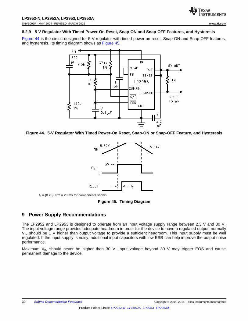
8.2.9 5-V Regulator With Timed Power-On Reset, Snap-ON and Snap-OFF Features, and HysteresisFigure 44 is the circuit designed for 5-V regulator with timed power-on reset, Snap-ON and Snap-OFF features,and hysteresis. Its timing diagram shows as Figure 45.
Figure 44. 5-V Regulator With Timed Power-On Reset, Snap-ON or Snap-OFF Feature, and Hysteresis
td = (0.28), RC = 28 ms for components shown.
Figure 45. Timing Diagram
9 Power Supply Recommendations
The LP2952 and LP2953 is designed to operate from an input voltage supply range between 2.3 V and 30 V.The input voltage range provides adequate headroom in order for the device to have a regulated output, normallyVIN should be 1 V higher than output voltage to provide a sufficient headroom. This input supply must be wellregulated. If the input supply is noisy, additional input capacitors with low ESR can help improve the output noiseperformance.
Maximum VIN should never be higher than 30 V. Input voltage beyond 30 V may trigger EOS and causepermanent damage to the device.
30 Submit Documentation Feedback Copyright © 2004–2015, Texas Instruments Incorporated
Product Folder Links: LP2952-N LP2952A LP2953 LP2953A
Ground
VOUT
VIN
Input Capacitor
Output Capacitor
GND
NC
OUT
SENSE VTAP
GROUND
FEEDBACK
IN
Error Pullup Resistor
Vout
SHUTDOWN
ERROR
NC
GROUND GROUND
REFERENCE
NC
NC
LP2952-N, LP2952A, LP2953, LP2953Awww.ti.com SNVS095F –MAY 2004–REVISED MARCH 2015
10 Layout
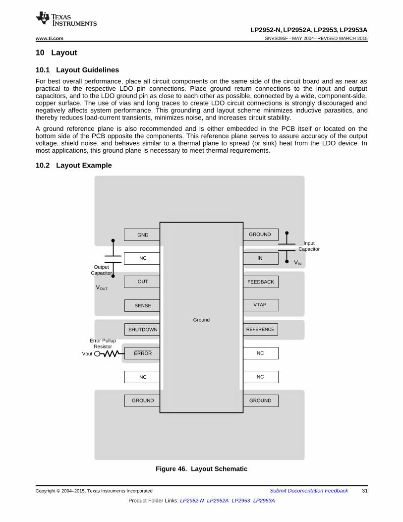
10.1 Layout GuidelinesFor best overall performance, place all circuit components on the same side of the circuit board and as near aspractical to the respective LDO pin connections. Place ground return connections to the input and outputcapacitors, and to the LDO ground pin as close to each other as possible, connected by a wide, component-side,copper surface. The use of vias and long traces to create LDO circuit connections is strongly discouraged andnegatively affects system performance. This grounding and layout scheme minimizes inductive parasitics, andthereby reduces load-current transients, minimizes noise, and increases circuit stability.
A ground reference plane is also recommended and is either embedded in the PCB itself or located on thebottom side of the PCB opposite the components. This reference plane serves to assure accuracy of the outputvoltage, shield noise, and behaves similar to a thermal plane to spread (or sink) heat from the LDO device. Inmost applications, this ground plane is necessary to meet thermal requirements.
10.2 Layout Example
Figure 46. Layout Schematic
Copyright © 2004–2015, Texas Instruments Incorporated Submit Documentation Feedback 31
Product Folder Links: LP2952-N LP2952A LP2953 LP2953A
LP2952-N, LP2952A, LP2953, LP2953ASNVS095F –MAY 2004–REVISED MARCH 2015 www.ti.com
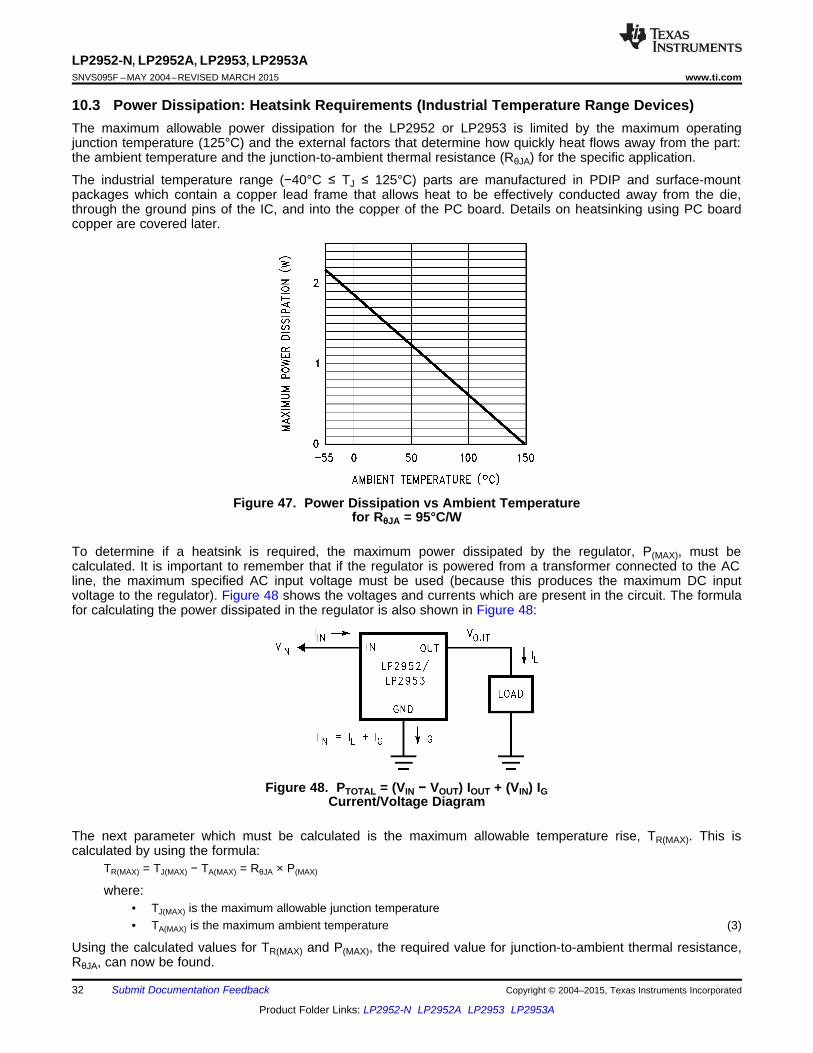
10.3 Power Dissipation: Heatsink Requirements (Industrial Temperature Range Devices)The maximum allowable power dissipation for the LP2952 or LP2953 is limited by the maximum operatingjunction temperature (125°C) and the external factors that determine how quickly heat flows away from the part:the ambient temperature and the junction-to-ambient thermal resistance (RθJA) for the specific application.
The industrial temperature range (−40°C ≤ TJ ≤ 125°C) parts are manufactured in PDIP and surface-mountpackages which contain a copper lead frame that allows heat to be effectively conducted away from the die,through the ground pins of the IC, and into the copper of the PC board. Details on heatsinking using PC boardcopper are covered later.
Figure 47. Power Dissipation vs Ambient Temperaturefor RθJA = 95°C/W
To determine if a heatsink is required, the maximum power dissipated by the regulator, P(MAX), must becalculated. It is important to remember that if the regulator is powered from a transformer connected to the ACline, the maximum specified AC input voltage must be used (because this produces the maximum DC inputvoltage to the regulator). Figure 48 shows the voltages and currents which are present in the circuit. The formulafor calculating the power dissipated in the regulator is also shown in Figure 48:
Figure 48. PTOTAL = (VIN − VOUT) IOUT + (VIN) IGCurrent/Voltage Diagram
The next parameter which must be calculated is the maximum allowable temperature rise, TR(MAX). This iscalculated by using the formula:
TR(MAX) = TJ(MAX) − TA(MAX) = RθJA × P(MAX)
where:• TJ(MAX) is the maximum allowable junction temperature• TA(MAX) is the maximum ambient temperature (3)
Using the calculated values for TR(MAX) and P(MAX), the required value for junction-to-ambient thermal resistance,RθJA, can now be found.
32 Submit Documentation Feedback Copyright © 2004–2015, Texas Instruments Incorporated
Product Folder Links: LP2952-N LP2952A LP2953 LP2953A
LP2952-N, LP2952A, LP2953, LP2953Awww.ti.com SNVS095F –MAY 2004–REVISED MARCH 2015
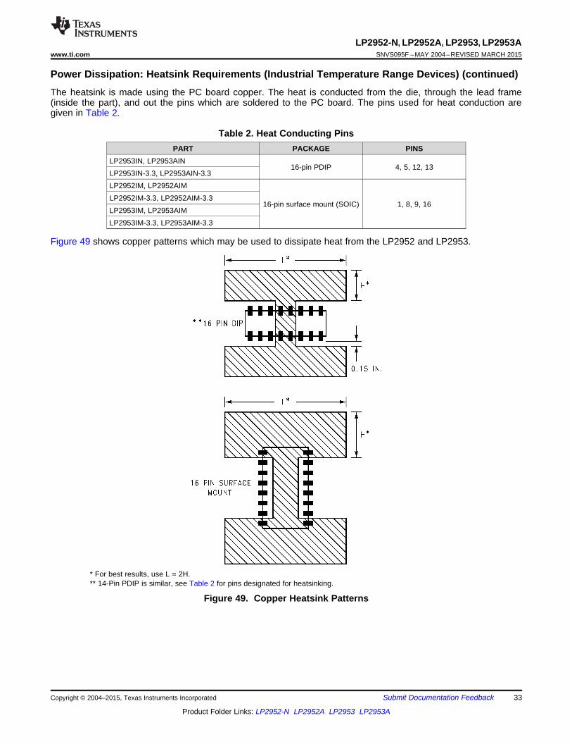
Power Dissipation: Heatsink Requirements (Industrial Temperature Range Devices) (continued)The heatsink is made using the PC board copper. The heat is conducted from the die, through the lead frame(inside the part), and out the pins which are soldered to the PC board. The pins used for heat conduction aregiven in Table 2.
Table 2. Heat Conducting PinsPART PACKAGE PINS
LP2953IN, LP2953AIN16-pin PDIP 4, 5, 12, 13
LP2953IN-3.3, LP2953AIN-3.3LP2952IM, LP2952AIMLP2952IM-3.3, LP2952AIM-3.3
16-pin surface mount (SOIC) 1, 8, 9, 16LP2953IM, LP2953AIMLP2953IM-3.3, LP2953AIM-3.3
Figure 49 shows copper patterns which may be used to dissipate heat from the LP2952 and LP2953.
* For best results, use L = 2H.** 14-Pin PDIP is similar, see Table 2 for pins designated for heatsinking.
Figure 49. Copper Heatsink Patterns
Copyright © 2004–2015, Texas Instruments Incorporated Submit Documentation Feedback 33
Product Folder Links: LP2952-N LP2952A LP2953 LP2953A
LP2952-N, LP2952A, LP2953, LP2953ASNVS095F –MAY 2004–REVISED MARCH 2015 www.ti.com
11 Device and Documentation Support
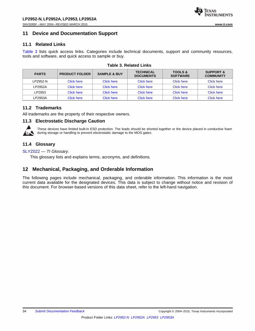
11.1 Related LinksTable 3 lists quick access links. Categories include technical documents, support and community resources,tools and software, and quick access to sample or buy.
Table 3. Related LinksTECHNICAL TOOLS & SUPPORT &PARTS PRODUCT FOLDER SAMPLE & BUY DOCUMENTS SOFTWARE COMMUNITY
LP2952-N Click here Click here Click here Click here Click hereLP2952A Click here Click here Click here Click here Click hereLP2953 Click here Click here Click here Click here Click here
LP2953A Click here Click here Click here Click here Click here
11.2 TrademarksAll trademarks are the property of their respective owners.
11.3 Electrostatic Discharge CautionThese devices have limited built-in ESD protection. The leads should be shorted together or the device placed in conductive foamduring storage or handling to prevent electrostatic damage to the MOS gates.
11.4 GlossarySLYZ022 — TI Glossary.
This glossary lists and explains terms, acronyms, and definitions.
12 Mechanical, Packaging, and Orderable InformationThe following pages include mechanical, packaging, and orderable information. This information is the mostcurrent data available for the designated devices. This data is subject to change without notice and revision ofthis document. For browser-based versions of this data sheet, refer to the left-hand navigation.
34 Submit Documentation Feedback Copyright © 2004–2015, Texas Instruments Incorporated
Product Folder Links: LP2952-N LP2952A LP2953 LP2953A
PACKAGE OPTION ADDENDUM
www.ti.com 2-Aug-2017
Addendum-Page 1
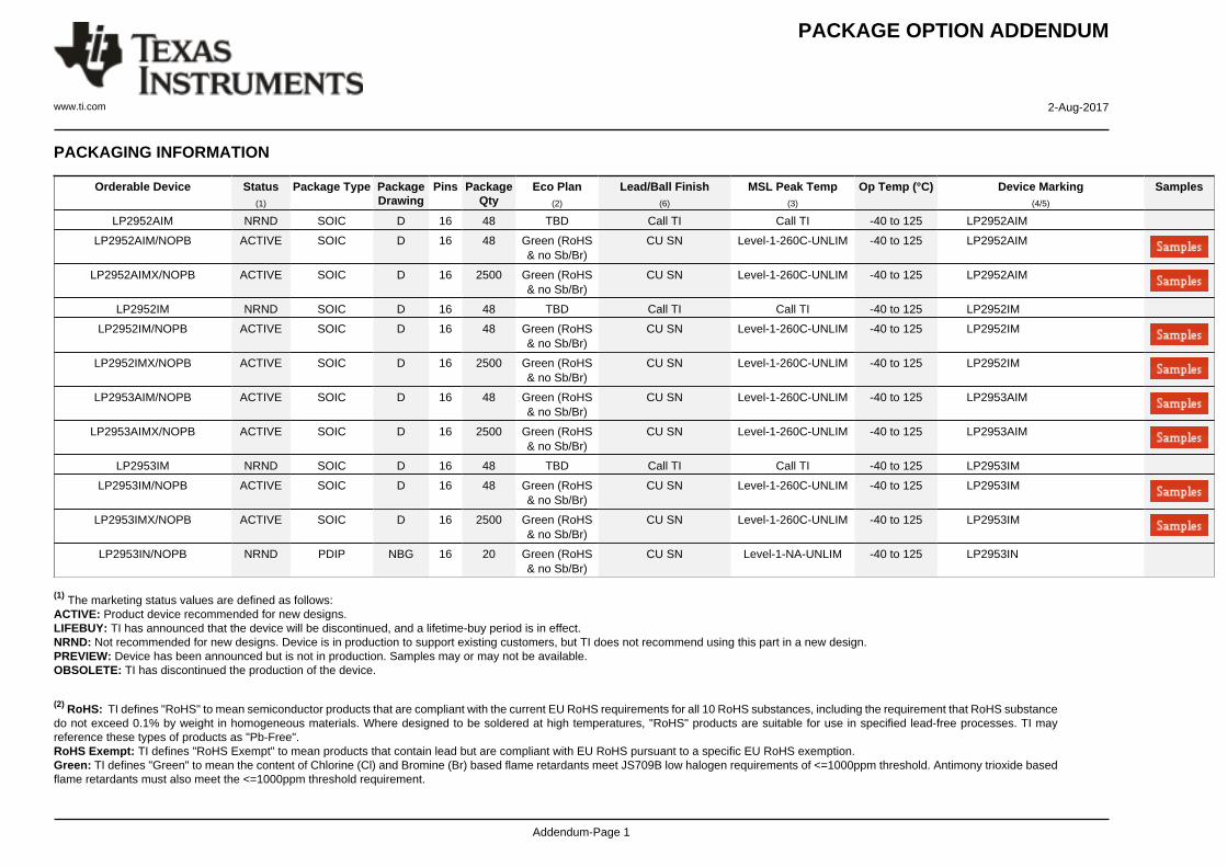
PACKAGING INFORMATION
Orderable Device Status(1)
Package Type PackageDrawing
Pins PackageQty
Eco Plan(2)
Lead/Ball Finish(6)
MSL Peak Temp(3)
Op Temp (°C) Device Marking(4/5)
Samples
LP2952AIM NRND SOIC D 16 48 TBD Call TI Call TI -40 to 125 LP2952AIM
LP2952AIM/NOPB ACTIVE SOIC D 16 48 Green (RoHS& no Sb/Br)
CU SN Level-1-260C-UNLIM -40 to 125 LP2952AIM
LP2952AIMX/NOPB ACTIVE SOIC D 16 2500 Green (RoHS& no Sb/Br)
CU SN Level-1-260C-UNLIM -40 to 125 LP2952AIM
LP2952IM NRND SOIC D 16 48 TBD Call TI Call TI -40 to 125 LP2952IM
LP2952IM/NOPB ACTIVE SOIC D 16 48 Green (RoHS& no Sb/Br)
CU SN Level-1-260C-UNLIM -40 to 125 LP2952IM
LP2952IMX/NOPB ACTIVE SOIC D 16 2500 Green (RoHS& no Sb/Br)
CU SN Level-1-260C-UNLIM -40 to 125 LP2952IM
LP2953AIM/NOPB ACTIVE SOIC D 16 48 Green (RoHS& no Sb/Br)
CU SN Level-1-260C-UNLIM -40 to 125 LP2953AIM
LP2953AIMX/NOPB ACTIVE SOIC D 16 2500 Green (RoHS& no Sb/Br)
CU SN Level-1-260C-UNLIM -40 to 125 LP2953AIM
LP2953IM NRND SOIC D 16 48 TBD Call TI Call TI -40 to 125 LP2953IM
LP2953IM/NOPB ACTIVE SOIC D 16 48 Green (RoHS& no Sb/Br)
CU SN Level-1-260C-UNLIM -40 to 125 LP2953IM
LP2953IMX/NOPB ACTIVE SOIC D 16 2500 Green (RoHS& no Sb/Br)
CU SN Level-1-260C-UNLIM -40 to 125 LP2953IM
LP2953IN/NOPB NRND PDIP NBG 16 20 Green (RoHS& no Sb/Br)
CU SN Level-1-NA-UNLIM -40 to 125 LP2953IN
(1) The marketing status values are defined as follows:ACTIVE: Product device recommended for new designs.LIFEBUY: TI has announced that the device will be discontinued, and a lifetime-buy period is in effect.NRND: Not recommended for new designs. Device is in production to support existing customers, but TI does not recommend using this part in a new design.PREVIEW: Device has been announced but is not in production. Samples may or may not be available.OBSOLETE: TI has discontinued the production of the device.
(2) RoHS: TI defines "RoHS" to mean semiconductor products that are compliant with the current EU RoHS requirements for all 10 RoHS substances, including the requirement that RoHS substancedo not exceed 0.1% by weight in homogeneous materials. Where designed to be soldered at high temperatures, "RoHS" products are suitable for use in specified lead-free processes. TI mayreference these types of products as "Pb-Free".RoHS Exempt: TI defines "RoHS Exempt" to mean products that contain lead but are compliant with EU RoHS pursuant to a specific EU RoHS exemption.Green: TI defines "Green" to mean the content of Chlorine (Cl) and Bromine (Br) based flame retardants meet JS709B low halogen requirements of <=1000ppm threshold. Antimony trioxide basedflame retardants must also meet the <=1000ppm threshold requirement.
PACKAGE OPTION ADDENDUM
www.ti.com 2-Aug-2017
Addendum-Page 2
(3) MSL, Peak Temp. - The Moisture Sensitivity Level rating according to the JEDEC industry standard classifications, and peak solder temperature.
(4) There may be additional marking, which relates to the logo, the lot trace code information, or the environmental category on the device.
(5) Multiple Device Markings will be inside parentheses. Only one Device Marking contained in parentheses and separated by a "~" will appear on a device. If a line is indented then it is a continuationof the previous line and the two combined represent the entire Device Marking for that device.
(6) Lead/Ball Finish - Orderable Devices may have multiple material finish options. Finish options are separated by a vertical ruled line. Lead/Ball Finish values may wrap to two lines if the finishvalue exceeds the maximum column width.
Important Information and Disclaimer:The information provided on this page represents TI's knowledge and belief as of the date that it is provided. TI bases its knowledge and belief on informationprovided by third parties, and makes no representation or warranty as to the accuracy of such information. Efforts are underway to better integrate information from third parties. TI has taken andcontinues to take reasonable steps to provide representative and accurate information but may not have conducted destructive testing or chemical analysis on incoming materials and chemicals.TI and TI suppliers consider certain information to be proprietary, and thus CAS numbers and other limited information may not be available for release.
In no event shall TI's liability arising out of such information exceed the total purchase price of the TI part(s) at issue in this document sold by TI to Customer on an annual basis.
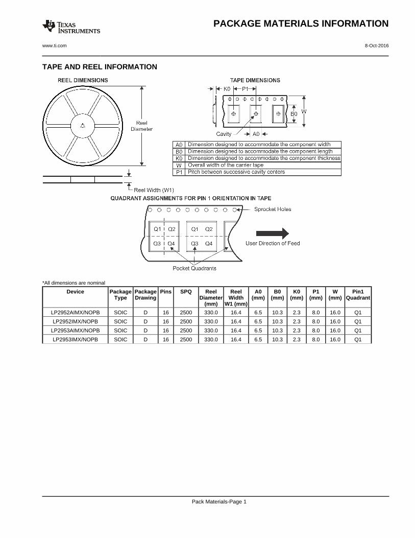
TAPE AND REEL INFORMATION
*All dimensions are nominal
Device PackageType
PackageDrawing
Pins SPQ ReelDiameter
(mm)
ReelWidth
W1 (mm)
A0(mm)
B0(mm)
K0(mm)
P1(mm)
W(mm)
Pin1Quadrant
LP2952AIMX/NOPB SOIC D 16 2500 330.0 16.4 6.5 10.3 2.3 8.0 16.0 Q1
LP2952IMX/NOPB SOIC D 16 2500 330.0 16.4 6.5 10.3 2.3 8.0 16.0 Q1
LP2953AIMX/NOPB SOIC D 16 2500 330.0 16.4 6.5 10.3 2.3 8.0 16.0 Q1
LP2953IMX/NOPB SOIC D 16 2500 330.0 16.4 6.5 10.3 2.3 8.0 16.0 Q1
PACKAGE MATERIALS INFORMATION
www.ti.com 8-Oct-2016
Pack Materials-Page 1
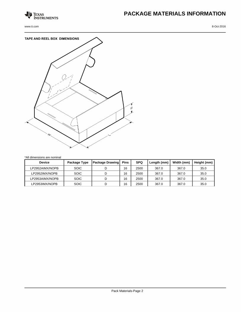
*All dimensions are nominal
Device Package Type Package Drawing Pins SPQ Length (mm) Width (mm) Height (mm)
LP2952AIMX/NOPB SOIC D 16 2500 367.0 367.0 35.0
LP2952IMX/NOPB SOIC D 16 2500 367.0 367.0 35.0
LP2953AIMX/NOPB SOIC D 16 2500 367.0 367.0 35.0
LP2953IMX/NOPB SOIC D 16 2500 367.0 367.0 35.0
PACKAGE MATERIALS INFORMATION
www.ti.com 8-Oct-2016
Pack Materials-Page 2
MECHANICAL DATA
NBG0016G
www.ti.com
IMPORTANT NOTICE
Texas Instruments Incorporated (TI) reserves the right to make corrections, enhancements, improvements and other changes to itssemiconductor products and services per JESD46, latest issue, and to discontinue any product or service per JESD48, latest issue. Buyersshould obtain the latest relevant information before placing orders and should verify that such information is current and complete.TI’s published terms of sale for semiconductor products (http://www.ti.com/sc/docs/stdterms.htm) apply to the sale of packaged integratedcircuit products that TI has qualified and released to market. Additional terms may apply to the use or sale of other types of TI products andservices.Reproduction of significant portions of TI information in TI data sheets is permissible only if reproduction is without alteration and isaccompanied by all associated warranties, conditions, limitations, and notices. TI is not responsible or liable for such reproduceddocumentation. Information of third parties may be subject to additional restrictions. Resale of TI products or services with statementsdifferent from or beyond the parameters stated by TI for that product or service voids all express and any implied warranties for theassociated TI product or service and is an unfair and deceptive business practice. TI is not responsible or liable for any such statements.Buyers and others who are developing systems that incorporate TI products (collectively, “Designers”) understand and agree that Designersremain responsible for using their independent analysis, evaluation and judgment in designing their applications and that Designers havefull and exclusive responsibility to assure the safety of Designers' applications and compliance of their applications (and of all TI productsused in or for Designers’ applications) with all applicable regulations, laws and other applicable requirements. Designer represents that, withrespect to their applications, Designer has all the necessary expertise to create and implement safeguards that (1) anticipate dangerousconsequences of failures, (2) monitor failures and their consequences, and (3) lessen the likelihood of failures that might cause harm andtake appropriate actions. Designer agrees that prior to using or distributing any applications that include TI products, Designer willthoroughly test such applications and the functionality of such TI products as used in such applications.TI’s provision of technical, application or other design advice, quality characterization, reliability data or other services or information,including, but not limited to, reference designs and materials relating to evaluation modules, (collectively, “TI Resources”) are intended toassist designers who are developing applications that incorporate TI products; by downloading, accessing or using TI Resources in anyway, Designer (individually or, if Designer is acting on behalf of a company, Designer’s company) agrees to use any particular TI Resourcesolely for this purpose and subject to the terms of this Notice.TI’s provision of TI Resources does not expand or otherwise alter TI’s applicable published warranties or warranty disclaimers for TIproducts, and no additional obligations or liabilities arise from TI providing such TI Resources. TI reserves the right to make corrections,enhancements, improvements and other changes to its TI Resources. TI has not conducted any testing other than that specificallydescribed in the published documentation for a particular TI Resource.Designer is authorized to use, copy and modify any individual TI Resource only in connection with the development of applications thatinclude the TI product(s) identified in such TI Resource. NO OTHER LICENSE, EXPRESS OR IMPLIED, BY ESTOPPEL OR OTHERWISETO ANY OTHER TI INTELLECTUAL PROPERTY RIGHT, AND NO LICENSE TO ANY TECHNOLOGY OR INTELLECTUAL PROPERTYRIGHT OF TI OR ANY THIRD PARTY IS GRANTED HEREIN, including but not limited to any patent right, copyright, mask work right, orother intellectual property right relating to any combination, machine, or process in which TI products or services are used. Informationregarding or referencing third-party products or services does not constitute a license to use such products or services, or a warranty orendorsement thereof. Use of TI Resources may require a license from a third party under the patents or other intellectual property of thethird party, or a license from TI under the patents or other intellectual property of TI.TI RESOURCES ARE PROVIDED “AS IS” AND WITH ALL FAULTS. TI DISCLAIMS ALL OTHER WARRANTIES ORREPRESENTATIONS, EXPRESS OR IMPLIED, REGARDING RESOURCES OR USE THEREOF, INCLUDING BUT NOT LIMITED TOACCURACY OR COMPLETENESS, TITLE, ANY EPIDEMIC FAILURE WARRANTY AND ANY IMPLIED WARRANTIES OFMERCHANTABILITY, FITNESS FOR A PARTICULAR PURPOSE, AND NON-INFRINGEMENT OF ANY THIRD PARTY INTELLECTUALPROPERTY RIGHTS. TI SHALL NOT BE LIABLE FOR AND SHALL NOT DEFEND OR INDEMNIFY DESIGNER AGAINST ANY CLAIM,INCLUDING BUT NOT LIMITED TO ANY INFRINGEMENT CLAIM THAT RELATES TO OR IS BASED ON ANY COMBINATION OFPRODUCTS EVEN IF DESCRIBED IN TI RESOURCES OR OTHERWISE. IN NO EVENT SHALL TI BE LIABLE FOR ANY ACTUAL,DIRECT, SPECIAL, COLLATERAL, INDIRECT, PUNITIVE, INCIDENTAL, CONSEQUENTIAL OR EXEMPLARY DAMAGES INCONNECTION WITH OR ARISING OUT OF TI RESOURCES OR USE THEREOF, AND REGARDLESS OF WHETHER TI HAS BEENADVISED OF THE POSSIBILITY OF SUCH DAMAGES.Unless TI has explicitly designated an individual product as meeting the requirements of a particular industry standard (e.g., ISO/TS 16949and ISO 26262), TI is not responsible for any failure to meet such industry standard requirements.Where TI specifically promotes products as facilitating functional safety or as compliant with industry functional safety standards, suchproducts are intended to help enable customers to design and create their own applications that meet applicable functional safety standardsand requirements. Using products in an application does not by itself establish any safety features in the application. Designers mustensure compliance with safety-related requirements and standards applicable to their applications. Designer may not use any TI products inlife-critical medical equipment unless authorized officers of the parties have executed a special contract specifically governing such use.Life-critical medical equipment is medical equipment where failure of such equipment would cause serious bodily injury or death (e.g., lifesupport, pacemakers, defibrillators, heart pumps, neurostimulators, and implantables). Such equipment includes, without limitation, allmedical devices identified by the U.S. Food and Drug Administration as Class III devices and equivalent classifications outside the U.S.TI may expressly designate certain products as completing a particular qualification (e.g., Q100, Military Grade, or Enhanced Product).Designers agree that it has the necessary expertise to select the product with the appropriate qualification designation for their applicationsand that proper product selection is at Designers’ own risk. Designers are solely responsible for compliance with all legal and regulatoryrequirements in connection with such selection.Designer will fully indemnify TI and its representatives against any damages, costs, losses, and/or liabilities arising out of Designer’s non-compliance with the terms and provisions of this Notice.
Mailing Address: Texas Instruments, Post Office Box 655303, Dallas, Texas 75265Copyright © 2017, Texas Instruments Incorporated