Embed Size (px)
Citation preview
MCU
LP8550
SWFB
VLDO
GNDs
EN
ISET
VDDIO
PWM
SCLKSDA
OUT1
OUT2
OUT3
OUT4
OUT5
OUT6
L1 D110V ± 40V
5.5V ± 22V
FILTER
5V
FSET
15 éH
VSYNC
210 mA ± 400 mA
COUTCIN
10 éF 4.7 éF
CVLDO
1 éF
VDDIO reference voltage
VSYNC signal
120 k5
100 nF
1 éF
FAULTCan be left floating
if not used
39 pF
VIN
RISET
RFSET
VBATT
0 10 20 30 40 50 60 70 80 90 10060
65
70
75
80
85
90
95
100
EF
FIC
IEN
CY
(%
)
DUTY CYCLE (%)
VIN = 9V
VIN = 12V
Product
Folder
Sample &Buy
Technical
Documents
Tools &
Software
Support &Community
LP8550SNVS657E –SEPTEMBER 2010–REVISED SEPTEMBER 2014
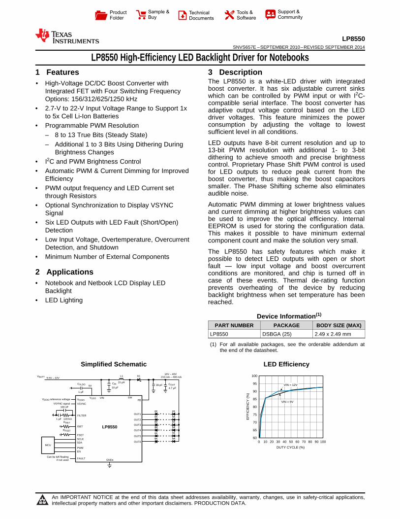
LP8550 High-Efficiency LED Backlight Driver for Notebooks1 Features 3 Description
The LP8550 is a white-LED driver with integrated1• High-Voltage DC/DC Boost Converter with
boost converter. It has six adjustable current sinksIntegrated FET with Four Switching Frequencywhich can be controlled by PWM input or with I2C-Options: 156/312/625/1250 kHz compatible serial interface. The boost converter has
• 2.7-V to 22-V Input Voltage Range to Support 1x adaptive output voltage control based on the LEDto 5x Cell Li-Ion Batteries driver voltages. This feature minimizes the power
consumption by adjusting the voltage to lowest• Programmable PWM Resolutionsufficient level in all conditions.– 8 to 13 True Bits (Steady State)LED outputs have 8-bit current resolution and up to– Additional 1 to 3 Bits Using Dithering During13-bit PWM resolution with additional 1- to 3-bitBrightness Changesdithering to achieve smooth and precise brightness• I2C and PWM Brightness Control control. Proprietary Phase Shift PWM control is used
• Automatic PWM & Current Dimming for Improved for LED outputs to reduce peak current from theEfficiency boost converter, thus making the boost capacitors
smaller. The Phase Shifting scheme also eliminates• PWM output frequency and LED Current setaudible noise.through ResistorsAutomatic PWM dimming at lower brightness values• Optional Synchronization to Display VSYNCand current dimming at higher brightness values canSignalbe used to improve the optical efficiency. Internal• Six LED Outputs with LED Fault (Short/Open) EEPROM is used for storing the configuration data.Detection This makes it possible to have minimum external
• Low Input Voltage, Overtemperature, Overcurrent component count and make the solution very small.Detection, and Shutdown The LP8550 has safety features which make it
• Minimum Number of External Components possible to detect LED outputs with open or shortfault — low input voltage and boost overcurrent
2 Applications conditions are monitored, and chip is turned off incase of these events. Thermal de-rating function• Notebook and Netbook LCD Display LEDprevents overheating of the device by reducingBacklight backlight brightness when set temperature has been
• LED Lighting reached.
Device Information(1)
PART NUMBER PACKAGE BODY SIZE (MAX)LP8550 DSBGA (25) 2.49 x 2.49 mm
(1) For all available packages, see the orderable addendum atthe end of the datasheet.
Simplified Schematic LED Efficiency
1
An IMPORTANT NOTICE at the end of this data sheet addresses availability, warranty, changes, use in safety-critical applications,intellectual property matters and other important disclaimers. PRODUCTION DATA.
LP8550SNVS657E –SEPTEMBER 2010–REVISED SEPTEMBER 2014 www.ti.com
Table of Contents1 Features .................................................................. 1 8 Detailed Description ............................................ 11
8.1 Overview ................................................................. 112 Applications ........................................................... 18.2 Functional Block Diagram ....................................... 123 Description ............................................................. 18.3 Feature Description................................................. 124 Revision History..................................................... 28.4 Device Functional Modes........................................ 215 Device Default Values ........................................... 38.5 Programming .......................................................... 226 Pin Configuration and Functions ......................... 48.6 Register Maps ......................................................... 267 Specifications......................................................... 5 9 Application and Implementation ........................ 367.1 Absolute Maximum Ratings ...................................... 59.1 Application Information............................................ 367.2 Handling Ratings ...................................................... 59.2 Typical Applications ............................................... 367.3 Recommended Operating Conditions....................... 5
10 Power Supply Recommendations ..................... 407.4 Thermal Information .................................................. 611 Layout................................................................... 407.5 Electrical Characteristics.......................................... 6
11.1 Layout Guidelines ................................................. 407.6 Boost Converter Electrical Characteristics ............. 611.2 Layout Examples................................................... 417.7 LED Driver Electrical Characteristics ....................... 7
12 Device and Documentation Support ................. 437.8 PWM Interface Characteristics ................................ 712.1 Trademarks ........................................................... 437.9 Undervoltage Protection .......................................... 812.2 Electrostatic Discharge Caution............................ 437.10 Logic Interface Characteristics............................... 812.3 Glossary ................................................................ 437.11 I2C Serial Bus Timing Parameters (SDA, SCLK) .. 8
13 Mechanical, Packaging, and Orderable7.12 Typical Characteristics ............................................ 9Information ........................................................... 43
4 Revision HistoryNOTE: Page numbers for previous revisions may differ from page numbers in the current version.
Changes from Revision D (November 2013) to Revision E Page
• Changed formatting to match new TI datasheet guidelines; added Device Information and Handling Ratings tables,Power Supply Recommendations, Layout, and Device and Documentation Support sections; moved some curves toApplication Curves section, reformatted Detailed Description and Application and Implementation sections, addingadditional content. ................................................................................................................................................................. 1
Changes from Revision C (May 2013) to Revision D Page
• Added note re EEPROM ...................................................................................................................................................... 25• Added note re: EEPROM ..................................................................................................................................................... 30
2 Submit Documentation Feedback Copyright © 2010–2014, Texas Instruments Incorporated
Product Folder Links: LP8550
LP8550www.ti.com SNVS657E –SEPTEMBER 2010–REVISED SEPTEMBER 2014
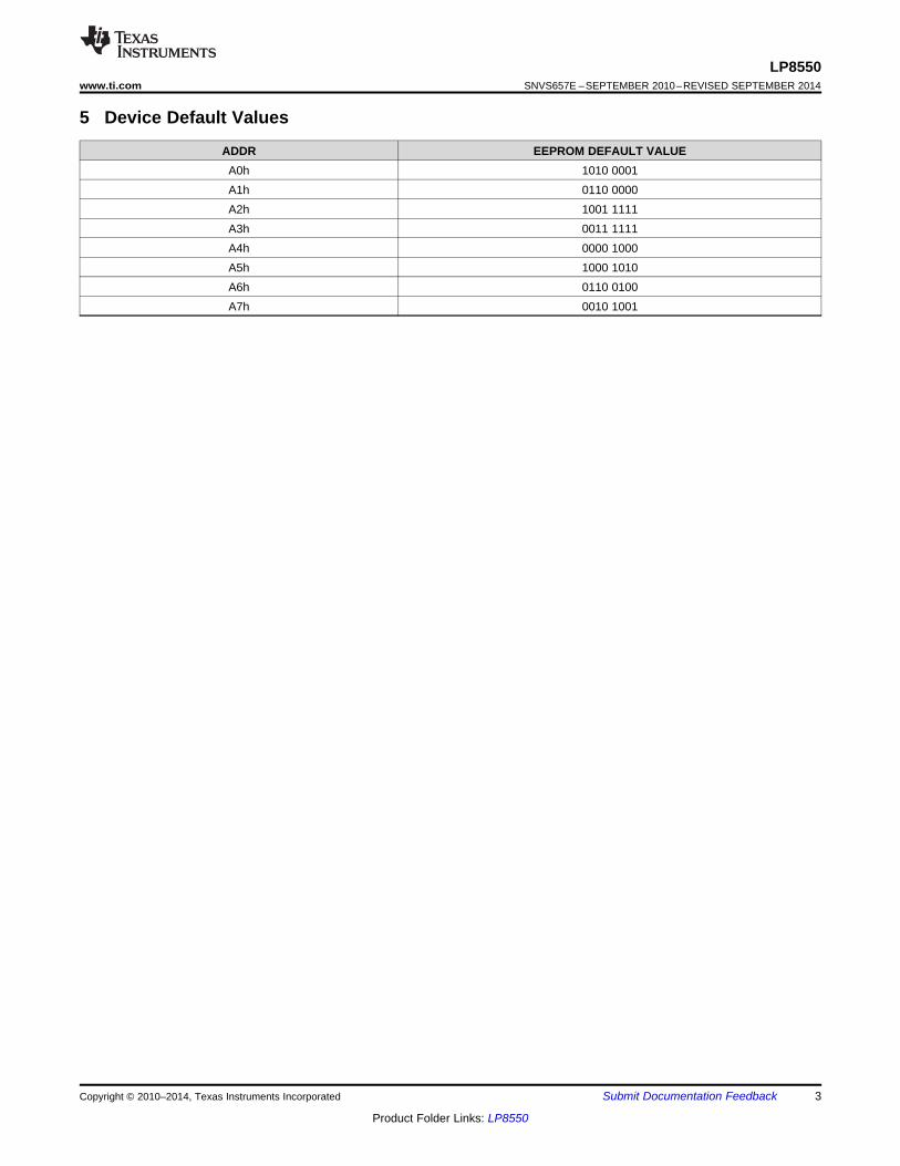
5 Device Default Values
ADDR EEPROM DEFAULT VALUEA0h 1010 0001A1h 0110 0000A2h 1001 1111A3h 0011 1111A4h 0000 1000A5h 1000 1010A6h 0110 0100A7h 0010 1001
Copyright © 2010–2014, Texas Instruments Incorporated Submit Documentation Feedback 3
Product Folder Links: LP8550
GND SW
GND SW
EN PWM FB
SW SW ISET FSET GND_S
VIN FILTER FAULT VDDIO OUT3
VLDO VSYNC SCLK SDA OUT2
OUT6 OUT5 OUT4 GND_L OUT1
A
B
C
D
E
1 2 3 4 5
GND SW
GND SW
ENPWMFB
SWSWISETFSETGND_S
VINFILTERFAULTVDDIOOUT3
VLDOVSYNCSCLKSDAOUT2
OUT6OUT5OUT4GND_LOUT1
A
B
C
D
E
12345
LP8550SNVS657E –SEPTEMBER 2010–REVISED SEPTEMBER 2014 www.ti.com
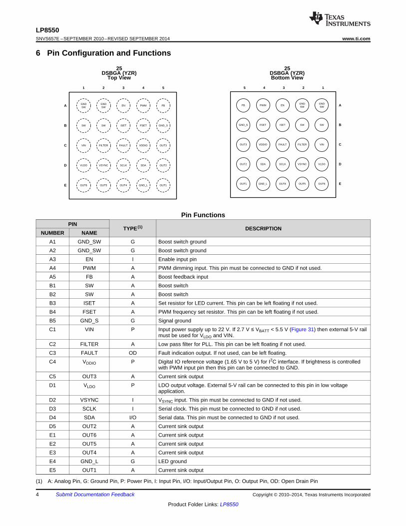
6 Pin Configuration and Functions
25 25DSBGA (YZR) DSBGA (YZR)
Top View Bottom View
Pin FunctionsPIN
TYPE (1) DESCRIPTIONNUMBER NAME
A1 GND_SW G Boost switch groundA2 GND_SW G Boost switch groundA3 EN I Enable input pinA4 PWM A PWM dimming input. This pin must be connected to GND if not used.A5 FB A Boost feedback inputB1 SW A Boost switchB2 SW A Boost switchB3 ISET A Set resistor for LED current. This pin can be left floating if not used.B4 FSET A PWM frequency set resistor. This pin can be left floating if not used.B5 GND_S G Signal groundC1 VIN P Input power supply up to 22 V. If 2.7 V ≤ VBATT < 5.5 V (Figure 31) then external 5-V rail
must be used for VLDO and VIN.C2 FILTER A Low pass filter for PLL. This pin can be left floating if not used.C3 FAULT OD Fault indication output. If not used, can be left floating.C4 VDDIO P Digital IO reference voltage (1.65 V to 5 V) for I2C interface. If brightness is controlled
with PWM input pin then this pin can be connected to GND.C5 OUT3 A Current sink outputD1 VLDO P LDO output voltage. External 5-V rail can be connected to this pin in low voltage
application.D2 VSYNC I VSYNC input. This pin must be connected to GND if not used.D3 SCLK I Serial clock. This pin must be connected to GND if not used.D4 SDA I/O Serial data. This pin must be connected to GND if not used.D5 OUT2 A Current sink outputE1 OUT6 A Current sink outputE2 OUT5 A Current sink outputE3 OUT4 A Current sink outputE4 GND_L G LED groundE5 OUT1 A Current sink output
(1) A: Analog Pin, G: Ground Pin, P: Power Pin, I: Input Pin, I/O: Input/Output Pin, O: Output Pin, OD: Open Drain Pin
4 Submit Documentation Feedback Copyright © 2010–2014, Texas Instruments Incorporated
Product Folder Links: LP8550

LP8550www.ti.com SNVS657E –SEPTEMBER 2010–REVISED SEPTEMBER 2014
7 Specifications
7.1 Absolute Maximum Ratingsover operating free-air temperature range (unless otherwise noted) (1) (2)
MIN MAX UNITVIN –0.3 24VLDO –0.3 6Voltage on logic pins (VSYNC, PWM, EN, SCLK, SDA) –0.3 6
V–0.3 VVDDIO +Voltage on logic pin (FAULT) 0.3Voltage on analog pins (FILTER, VDDIO, ISET, FSET) –0.3 6V (OUT1...OUT6, SW, FB) –0.3 44Continuous power dissipation (3) Internally LimitedJunction temperature (TJ-MAX) 125 °CMaximum lead temperature (soldering) See (4)
(1) Stresses beyond those listed under Absolute Maximum Ratings may cause permanent damage to the device. These are stress ratingsonly, which do not imply functional operation of the device at these or any other conditions beyond those indicated under RecommendedOperating Conditions. Exposure to absolute-maximum-rated conditions for extended periods may affect device reliability.
(2) If Military/Aerospace specified devices are required, please contact the TI Sales Office/Distributors for availability and specifications.(3) Internal thermal shutdown circuitry protects the device from permanent damage. Thermal shutdown engages at TJ = 150°C (typ.) and
disengages at TJ = 130°C (typ.).(4) For detailed soldering specifications and information, please refer to Application Report AN-1112 DSBGA Wafer Level Chip Scale
Package (SNVA009).
7.2 Handling RatingsMIN MAX UNIT
Tstg Storage temperature range –65 150 °CHuman body model (HBM), per ANSI/ESDA/JEDEC JS-001, all pins (1) -2 2 kV
ElectrostaticV(ESD) Charged device model (CDM), per JEDEC spec. JESD22-C101, all pins (2) –200 200 VdischargeMachine model –1 1 kV
(1) JEDEC document JEP155 states that 500-V HBM allows safe manufacturing with a standard ESD control process.(2) JEDEC document JEP157 states that 250-V CDM allows safe manufacturing with a standard ESD control process.
7.3 Recommended Operating Conditionsover operating free-air temperature range (unless otherwise noted) (1) (2)
MIN NOM MAX UNITVIN (Figure 27) 5.5 22
Input voltage rangeVIN + VLDO (Figure 31) 4.5 5.5
VVDDIO 1.65 5V(OUT1...OUT6, SW, FB) 0 40TJ Junction temperature –30 125
°CTA
(3) Ambient temperature –30 85
(1) Stresses beyond those listed under Absolute Maximum Ratings may cause permanent damage to the device. These are stress ratingsonly, which do not imply functional operation of the device at these or any other conditions beyond those indicated under RecommendedOperating Conditions. Exposure to absolute-maximum-rated conditions for extended periods may affect device reliability.
(2) All voltages are with respect to the potential at the GND pins.(3) In applications where high power dissipation and/or poor package thermal resistance is present, the maximum ambient temperature may
have to be derated. Maximum ambient temperature (TA-MAX) is dependent on the maximum operating junction temperature (TJ-MAX-OP =125°C), the maximum power dissipation of the device in the application (PD-MAX), and the junction-to ambient thermal resistance of thepart/package in the application (RθJA), as given by the following equation: TA-MAX = TJ-MAX-OP – (RθJA × PD-MAX).
Copyright © 2010–2014, Texas Instruments Incorporated Submit Documentation Feedback 5
Product Folder Links: LP8550
LP8550SNVS657E –SEPTEMBER 2010–REVISED SEPTEMBER 2014 www.ti.com
7.4 Thermal InformationDSBGA
THERMAL METRIC (1) UNIT25 PINS
RθJA Junction-to-ambient thermal resistance (2) 40 - 73 °C/W
(1) For more information about traditional and new thermal metrics, see the IC Package Thermal Metrics application report, SPRA953.(2) Junction-to-ambient thermal resistance is highly application and board-layout dependent. In applications where high maximum power
dissipation exists, special care must be paid to thermal dissipation issues in board design.
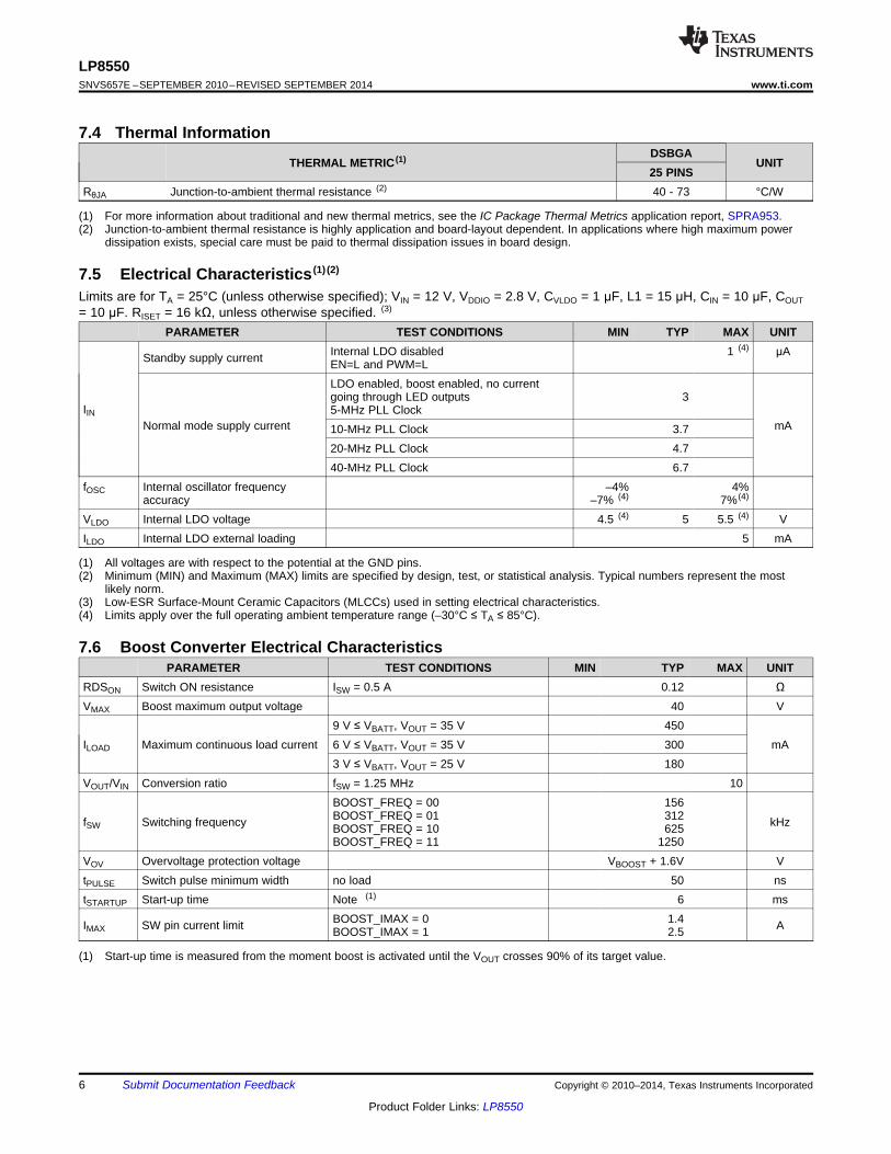
7.5 Electrical Characteristics (1) (2)
Limits are for TA = 25°C (unless otherwise specified); VIN = 12 V, VDDIO = 2.8 V, CVLDO = 1 μF, L1 = 15 μH, CIN = 10 μF, COUT= 10 μF. RISET = 16 kΩ, unless otherwise specified. (3)
PARAMETER TEST CONDITIONS MIN TYP MAX UNITInternal LDO disabled 1 (4) μAStandby supply current EN=L and PWM=LLDO enabled, boost enabled, no currentgoing through LED outputs 3
IIN 5-MHz PLL ClockNormal mode supply current mA10-MHz PLL Clock 3.7
20-MHz PLL Clock 4.740-MHz PLL Clock 6.7
fOSC Internal oscillator frequency –4% 4%accuracy –7% (4) 7% (4)
VLDO Internal LDO voltage 4.5 (4) 5 5.5 (4) VILDO Internal LDO external loading 5 mA
(1) All voltages are with respect to the potential at the GND pins.(2) Minimum (MIN) and Maximum (MAX) limits are specified by design, test, or statistical analysis. Typical numbers represent the most
likely norm.(3) Low-ESR Surface-Mount Ceramic Capacitors (MLCCs) used in setting electrical characteristics.(4) Limits apply over the full operating ambient temperature range (–30°C ≤ TA ≤ 85°C).
7.6 Boost Converter Electrical CharacteristicsPARAMETER TEST CONDITIONS MIN TYP MAX UNIT
RDSON Switch ON resistance ISW = 0.5 A 0.12 ΩVMAX Boost maximum output voltage 40 V
9 V ≤ VBATT, VOUT = 35 V 450ILOAD Maximum continuous load current 6 V ≤ VBATT, VOUT = 35 V 300 mA
3 V ≤ VBATT, VOUT = 25 V 180VOUT/VIN Conversion ratio fSW = 1.25 MHz 10
BOOST_FREQ = 00 156BOOST_FREQ = 01 312fSW Switching frequency kHzBOOST_FREQ = 10 625BOOST_FREQ = 11 1250
VOV Overvoltage protection voltage VBOOST + 1.6V VtPULSE Switch pulse minimum width no load 50 nstSTARTUP Start-up time Note (1) 6 ms
BOOST_IMAX = 0 1.4IMAX SW pin current limit ABOOST_IMAX = 1 2.5
(1) Start-up time is measured from the moment boost is activated until the VOUT crosses 90% of its target value.
6 Submit Documentation Feedback Copyright © 2010–2014, Texas Instruments Incorporated
Product Folder Links: LP8550
LP8550www.ti.com SNVS657E –SEPTEMBER 2010–REVISED SEPTEMBER 2014
7.7 LED Driver Electrical CharacteristicsPARAMETER TEST CONDITIONS MIN TYP MAX UNIT
ILEAKAGE Leakage current Outputs OUT1 to OUT6, VOUT = 40 V 0.1 1 μAEN_I_RES = 0, CURRENT[7:0] = FFh 30Maximum source current OUT1 toIMAX mAOUT6 EN_I_RES = 1, CURRENT[7:0] = FFh 50Output current set to 23 mA, EN_I_RES –3% 3%IOUT Output current accuracy (1)= 1 -4% (2) 4% (2)
Output current set to 23 mA, EN_I_RESIMATCH Matching (1) 0.5%= 1fLED = 5 kHz, fPLL = 5 MHz 10fLED = 10 kHz, fPLL = 5 MHz 9fLED = 20 kHz, fPLL = 5 MHz 8
PWMRES PWM output resolution (3) bitsfLED = 5 kHz, fPLL = 40 MHz 13fLED = 10 kHz, fPLL = 40 MHz 12fLED = 20 kHz, fPLL = 40 MHz 11PWM_FREQ[4:0] = 00000b 600PLL clock 5 MHz
fLED LED switching frequency (3) HzPWM_FREQ[4:0] = 11111b 19.2kPLL clock 5 MHzOutput current set to 20 mA 105 220 (5)
VSAT Saturation voltage (4) mVOutput current set to 30 mA 160 290 (5)
(1) Output Current Accuracy is the difference between the actual value of the output current and programmed value of this current.Matching is the maximum difference from the average. For the constant current sinks on the part (OUT1 to OUT6), the following aredetermined: the maximum output current (MAX), the minimum output current (MIN), and the average output current of all outputs (AVG).Two matching numbers are calculated: (MAX-AVG)/AVG and (AVG-MIN/AVG). The largest number of the two (worst case) isconsidered the matching figure. The typical specification provided is the most likely norm of the matching figure for all parts. Note thatsome manufacturers have different definitions in use.
(2) Limits apply over the full operating ambient temperature range (–30°C ≤ TA ≤ 85°C).(3) PWM output resolution and frequency depend on the PLL settings. Please see section PWM Frequency Setting for full description.(4) Saturation voltage is defined as the voltage when the LED current has dropped 10% from the value measured at 1 V.(5) Limits apply over the full operating ambient temperature range (–30°C ≤ TA ≤ 85°C).
7.8 PWM Interface CharacteristicsPARAMETER TEST CONDITIONS MIN TYP MAX UNIT
fPWM PWM frequency range 0.1 25 kHztMIN_ON Minimum pulse ON time 1
μstMIN_OFF Minimum pulse OFF time 1
Turnon delay from standby to PWM input active, EN pin rise from low totSTARTUP 6 msbacklight on highPWM input low time for turn off, slopeTSTBY Turn off delay 50 msdisabledfIN < 9 kHz 10fIN < 4.5 kHz 11PWMRES PWM input resolution bitsfIN < 2.2 kHz 12fIN < 1.1 kHz 13
Copyright © 2010–2014, Texas Instruments Incorporated Submit Documentation Feedback 7
Product Folder Links: LP8550
LP8550SNVS657E –SEPTEMBER 2010–REVISED SEPTEMBER 2014 www.ti.com
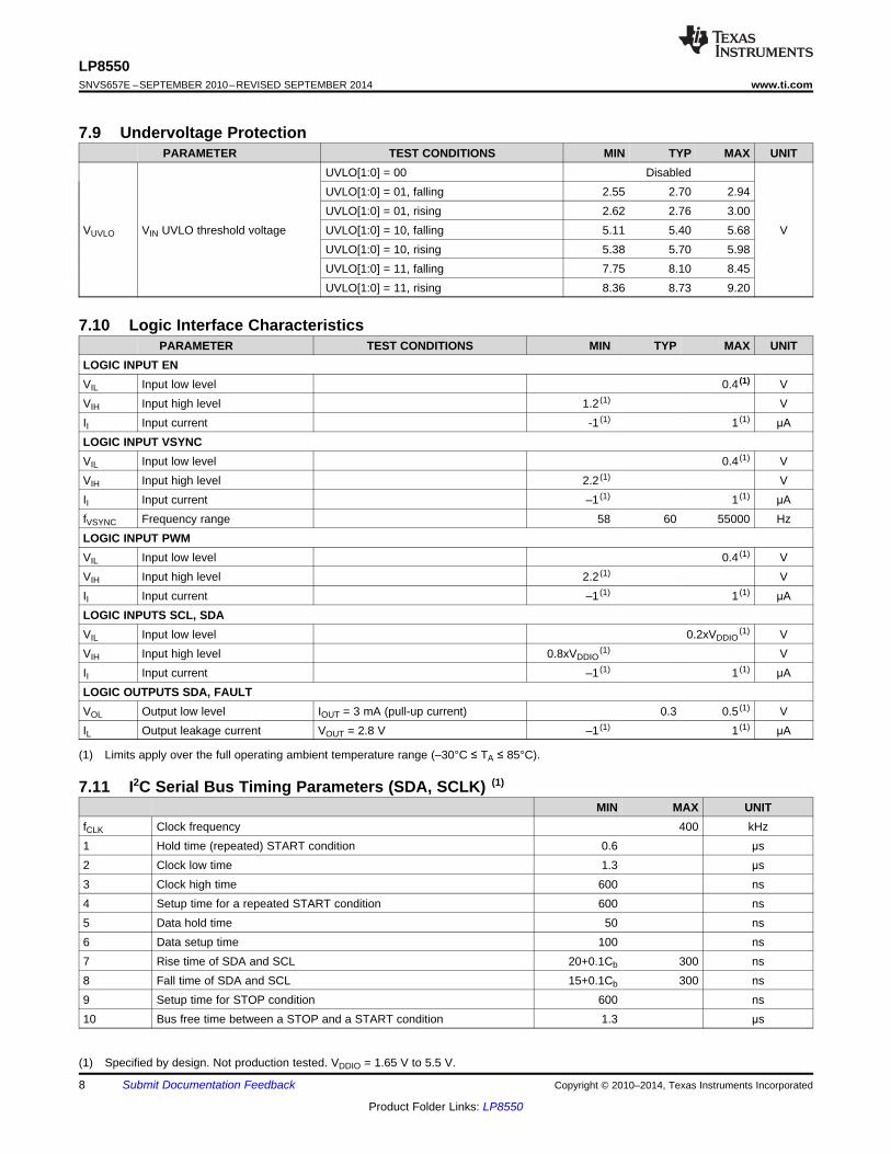
7.9 Undervoltage ProtectionPARAMETER TEST CONDITIONS MIN TYP MAX UNIT
UVLO[1:0] = 00 DisabledUVLO[1:0] = 01, falling 2.55 2.70 2.94UVLO[1:0] = 01, rising 2.62 2.76 3.00
VUVLO VIN UVLO threshold voltage UVLO[1:0] = 10, falling 5.11 5.40 5.68 VUVLO[1:0] = 10, rising 5.38 5.70 5.98UVLO[1:0] = 11, falling 7.75 8.10 8.45UVLO[1:0] = 11, rising 8.36 8.73 9.20
7.10 Logic Interface CharacteristicsPARAMETER TEST CONDITIONS MIN TYP MAX UNIT
LOGIC INPUT ENVIL Input low level 0.4 (1) VVIH Input high level 1.2 (1) VII Input current -1 (1) 1 (1) μALOGIC INPUT VSYNCVIL Input low level 0.4 (1) VVIH Input high level 2.2 (1) VII Input current –1 (1) 1 (1) μAfVSYNC Frequency range 58 60 55000 HzLOGIC INPUT PWMVIL Input low level 0.4 (1) VVIH Input high level 2.2 (1) VII Input current –1 (1) 1 (1) μALOGIC INPUTS SCL, SDAVIL Input low level 0.2xVDDIO
(1) VVIH Input high level 0.8xVDDIO
(1) VII Input current –1 (1) 1 (1) μALOGIC OUTPUTS SDA, FAULTVOL Output low level IOUT = 3 mA (pull-up current) 0.3 0.5 (1) VIL Output leakage current VOUT = 2.8 V –1 (1) 1 (1) μA
(1) Limits apply over the full operating ambient temperature range (–30°C ≤ TA ≤ 85°C).
7.11 I2C Serial Bus Timing Parameters (SDA, SCLK) (1)
MIN MAX UNITfCLK Clock frequency 400 kHz1 Hold time (repeated) START condition 0.6 μs2 Clock low time 1.3 μs3 Clock high time 600 ns4 Setup time for a repeated START condition 600 ns5 Data hold time 50 ns6 Data setup time 100 ns7 Rise time of SDA and SCL 20+0.1Cb 300 ns8 Fall time of SDA and SCL 15+0.1Cb 300 ns9 Setup time for STOP condition 600 ns10 Bus free time between a STOP and a START condition 1.3 μs
(1) Specified by design. Not production tested. VDDIO = 1.65 V to 5.5 V.
8 Submit Documentation Feedback Copyright © 2010–2014, Texas Instruments Incorporated
Product Folder Links: LP8550
0 50 100 150 200 250 30080
82
84
86
88
90
92
94
96
98
100
EF
FIC
IEN
CY
(%
)
IOUT (mA)
VBOOST = 30V
VBOOST = 35V
VBOOST = 40V
6 8 10 12 14 16 18 200
200
400
600
800
1,000
1,200
IBA
TT
(m
A)
VBATT (V)
LOAD = 150 mAVBOOST = 30V
VBOOST = 35V
VBOOST = 40V
0 10 20 30 40 50 60 70 80 90 10060
65
70
75
80
85
90
95
100
EF
FIC
IEN
CY
(%
)
DUTY CYCLE (%)
VIN = 9V
VIN = 12V
0 10 20 30 40 50 60 70 80 90 10060
65
70
75
80
85
90
95
100
EF
FIC
IEN
CY
(%
)
DUTY CYCLE (%)
VIN = 9V
VIN = 12V
LP8550www.ti.com SNVS657E –SEPTEMBER 2010–REVISED SEPTEMBER 2014
I2C Serial Bus Timing Parameters (SDA, SCLK) (1) (continued)MIN MAX UNIT
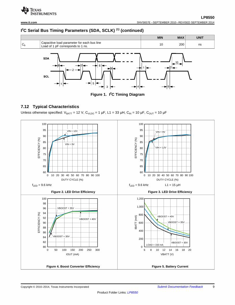
Capacitive load parameter for each bus lineCb 10 200 nsLoad of 1 pF corresponds to 1 ns.
Figure 1. I2C Timing Diagram
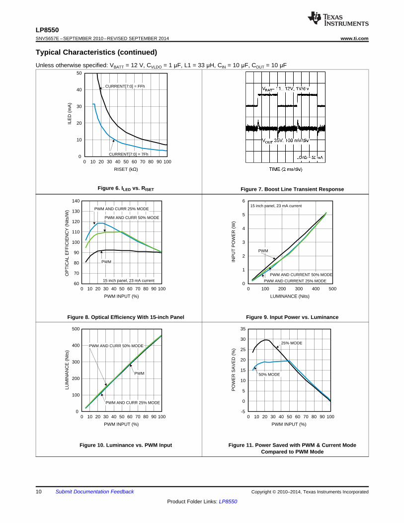
7.12 Typical CharacteristicsUnless otherwise specified: VBATT = 12 V, CVLDO = 1 μF, L1 = 33 μH, CIN = 10 μF, COUT = 10 μF
fLED = 9.6 kHz fLED = 9.6 kHz L1 = 15 µH
Figure 2. LED Drive Efficiency Figure 3. LED Drive Efficiency
Figure 4. Boost Converter Efficiency Figure 5. Battery Current
Copyright © 2010–2014, Texas Instruments Incorporated Submit Documentation Feedback 9
Product Folder Links: LP8550
0 10 20 30 40 50 60 70 80 90 1000
100
200
300
400
500
LUM
INA
NC
E (
Nits
)
PWM INPUT (%)
PWM
PWM AND CURR 25% MODE
PWM AND CURR 50% MODE
0 10 20 30 40 50 60 70 80 90 100-5
0
5
10
15
20
25
30
35
PO
WE
R S
AV
ED
(%
)
PWM INPUT (%)
25% MODE
50% MODE
0 10 20 30 40 50 60 70 80 90 10060
70
80
90
100
110
120
130
140
OP
TIC
AL
EF
FIC
IEN
CY
(N
its/W
)
PWM INPUT (%)
15 inch panel, 23 mA current
PWM AND CURR 25% MODE
PWM AND CURR 50% MODE
PWM
0 100 200 300 400 5000
1
2
3
4
5
6
INP
UT
PO
WE
R (
W)
LUMINANCE (Nits)
PWM
PWM AND CURRENT 25% MODE
PWM AND CURRENT 50% MODE
15 inch panel, 23 mA current
0 10 20 30 40 50 60 70 80 90 1000
10
20
30
40
50IL
ED
(m
A)
RISET (k )
CURRENT[7:0] = FFh
CURRENT[7:0] = 7Fh
LP8550SNVS657E –SEPTEMBER 2010–REVISED SEPTEMBER 2014 www.ti.com
Typical Characteristics (continued)Unless otherwise specified: VBATT = 12 V, CVLDO = 1 μF, L1 = 33 μH, CIN = 10 μF, COUT = 10 μF
Figure 6. ILED vs. RISET Figure 7. Boost Line Transient Response
Figure 8. Optical Efficiency With 15-inch Panel Figure 9. Input Power vs. Luminance
Figure 10. Luminance vs. PWM Input Figure 11. Power Saved with PWM & Current ModeCompared to PWM Mode
10 Submit Documentation Feedback Copyright © 2010–2014, Texas Instruments Incorporated
Product Folder Links: LP8550
LP8550www.ti.com SNVS657E –SEPTEMBER 2010–REVISED SEPTEMBER 2014
8 Detailed Description
8.1 OverviewLP8550 is a high voltage LED driver for medium-sized LCD backlight applications. It includes high voltage boostconverter. Boost voltage automatically sets to the correct level needed to drive the LED strings. This is done bymonitoring LED output voltage drop in real time.
Six LED outputs are driven either with constant current sinks with PWM control or by controlling both PWM andcurrent. Constant current value is set with EEPROM bits and with RISET resistor. Brightness (PWM) is controlledeither with I2C register or with PWM input. PWM frequencies are set with EEPROM bits and with RFSET resistor.Special Phase-Shift PWM mode can be used to reduce boost output current peak, thus reducing output ripple,capacitor size and audible noise.
With LP8550 it is possible to synchronize the PWM output frequency to VSYNC signal received from videoprocessor. Internal PLL ensures that the PWM output clock is always synchronized to the VSYNC signal.
Special dithering mode makes it possible to increase output resolution during fading between two brightnessvalues and by this making the transition look very smooth with virtually no stepping. Transition slope time can beadjusted with EEPROM bits.
Safety features include LED fault detection with open and short detection. LED fault detection prevents systemoverheating in case of open in some of the LED strings. Chip internal temperature is constantly monitored andbased on this LP8550 can reduce the brightness of the backlight to reduce thermal loading once certain trip pointis reached. Threshold is programmable in EEPROM. If chip internal temperature reaches too high, the boostconverter and LED outputs are completely turned off until the internal temperature has reached acceptable level.Boost converter is protected against too high load current and over-voltage. LP8550 notifies the system aboutthe fault through I2C register and with FAULT pin.
EEPROM programmable functions include:• PWM frequencies• Phase shift PWM mode• LED constant current• Boost output frequency• Temperature thresholds• Slope for brightness changes• Dithering options• PWM output resolution• Boost control bits
External components RISET and RFSET can also be used for selecting the output current and PWM frequencies.
Copyright © 2010–2014, Texas Instruments Incorporated Submit Documentation Feedback 11
Product Folder Links: LP8550
BOOST
LED DRIVERS
LOGIC
EEPROM
I2C /
INTERFACE
LDOOSCTSD
PWM DETECTOR
SW
FB
VLDO
GND
GND_SW
GND_LED
EN
PWM
VDDIO
SCLKSDA
OUT1
OUT2
OUT3
OUT4
OUT5
OUT6
PLL
FAULT
VIN
TEMP SENSOR
MCU
VIN
FILTER
VSYNC
VSYNC
ISET
FSET
RISET
RFSET
LP8550SNVS657E –SEPTEMBER 2010–REVISED SEPTEMBER 2014 www.ti.com
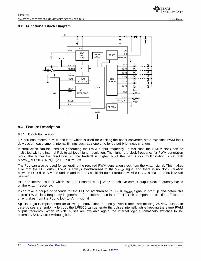
8.2 Functional Block Diagram
8.3 Feature Description
8.3.1 Clock GenerationLP8550 has internal 5-MHz oscillator which is used for clocking the boost converter, state machine, PWM inputduty cycle measurement, internal timings such as slope time for output brightness changes.
Internal clock can be used for generating the PWM output frequency. In this case the 5-MHz clock can bemultiplied with the internal PLL to achieve higher resolution. The higher the clock frequency for PWM generationblock, the higher the resolution but the tradeoff is higher IQ of the part. Clock multiplication is set with<PWM_RESOLUTION[1:0]> EEPROM Bits.
The PLL can also be used for generating the required PWM generation clock from the VSYNC signal. This makessure that the LED output PWM is always synchronized to the VSYNC signal and there is no clock variationbetween LCD display video update and the LED backlight output frequency. Also HSYNC signal up to 55 kHz canbe used.
PLL has internal counter which has 13-bit control <PLL[12:0]> to achieve correct output clock frequency basedon the VSYNC frequency.
It can take a couple of seconds for the PLL to synchronize to 60-Hz VSYNC signal in start-up and before thiscorrect PWM clock frequency is generated from internal oscillator. FILTER pin component selection affects thetime it takes from the PLL to lock to VSYNC signal.
Special logic is implemented for allowing steady clock frequency even if there are missing VSYNC pulses. Incase pulses are randomly left out, the LP8550 can generate the pulses internally while keeping the same PWMoutput frequency. When VSYNC pulses are available again, the internal logic automatically switches to theexternal VSYNC clock without glitch.
12 Submit Documentation Feedback Copyright © 2010–2014, Texas Instruments Incorporated
Product Folder Links: LP8550

5MHz internal oscillator
PLL[12:0]
PWM generation
PWM_FREQ[4:0]or External
set resistor RFSET
VBOOST
LED Drivers 1-6
Divider 1/N
5 MHz...40 MHz
PSPWM 0/1
Boost
Filter VCO
Counter1/N
PLL
VSYNC60 Hz EN_VSYNC
Phase Detector
State machine, PWM input, internal timings, Slope etc.
BOOST_FREQN = 4, 8, 16, 32
PWM_RESOLUTION[1:0]
LP8550www.ti.com SNVS657E –SEPTEMBER 2010–REVISED SEPTEMBER 2014
Feature Description (continued)
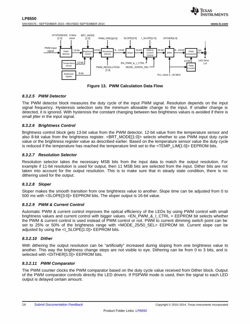
Figure 12. Principle Of The Clock Generation
8.3.2 Brightness Control MethodsLP8550 controls the brightness of the backlight with PWM. PWM control is received either from PWM input pin orfrom I2C register bits. The PWM source selection is done with <BRT_MODE[1:0]> bits as follows:
BRT_MODE[1] BRT_MODE[0] PWM SOURCE0 0 PWM input pin duty cycle control. Default.0 1 PWM input pin duty cycle control.1 0 Brightness register1 1 PWM direct control (PWM in = PWM out)
8.3.2.1 PWM Input Duty CycleWith PWM input pin duty cycle control the output PWM is controlled by PWM input duty cycle. PWM detectorblock measures the duty cycle in the PWM pin and uses this 13-bit value to generate the output PWM. OutputPWM can have different frequency than input in this mode and also phase shift PWM mode can be used. Slopeand dither are effective in this mode. PWM input resolution is defined by the input PWM clock frequency.
8.3.2.2 Brightness Register ControlWith brightness register control the output PWM is controlled with 8-bit resolution <BRT7:0> register bits. Phaseshift scheme can be used with this and the output PWM frequency can be freely selected. Slope and dither areeffective in this mode.
8.3.2.3 PWM Direct ControlWith PWM direct control the output PWM directly follows the input PWM. Due to the internal logic structure theinput is anyway clocked with the 5 MHz clock or the PLL clock. PSPWM mode is not possible in this mode. Slopeand dither are not effective in this mode.
8.3.2.4 PWM Calculation Data FlowFigure 13 shows a flow chart of the PWM calculation data flow. In PWM direct control mode most of the blocksare bypassed and this flow chart does not apply.
Copyright © 2010–2014, Texas Instruments Incorporated Submit Documentation Feedback 13
Product Folder Links: LP8550
PWM input signal PWM
detector
5 MHz clock
13-bit PWM comparator
PWMCounter
Brightness control
BRT_MODE[1:0]
Temperature sensor
12-bit
Brightness register
8-bit
Resolutionselector
13-bit
PWM_FREQ[4:0]
8...13-bit
SLOPE[3:0]
Dither16-bit
DITHER[1:0]
8...16-bit Sloper
13-bit
0/1
LED Drive1-6
PLL clock 5...40 MHz
PWM_RESOLUTION[1:0]
HYSTERESIS[1:0]
...PWM & Current Control
16-bit
I_SLOPE[1:0]
MODE_25/50%_SEL
EN_PWM_&_I_CTRL
LP8550SNVS657E –SEPTEMBER 2010–REVISED SEPTEMBER 2014 www.ti.com
Figure 13. PWM Calculation Data Flow
8.3.2.5 PWM DetectorThe PWM detector block measures the duty cycle of the input PWM signal. Resolution depends on the inputsignal frequency. Hysteresis selection sets the minimum allowable change to the input. If smaller change isdetected, it is ignored. With hysteresis the constant changing between two brightness values is avoided if there issmall jitter in the input signal.
8.3.2.6 Brightness ControlBrightness control block gets 13-bit value from the PWM detector, 12-bit value from the temperature sensor andalso 8-bit value from the brightness register. <BRT_MODE[1:0]> selects whether to use PWM input duty cyclevalue or the brightness register value as described earlier. Based on the temperature sensor value the duty cycleis reduced if the temperature has reached the temperature limit set to the <TEMP_LIM[1:0]> EEPROM bits.
8.3.2.7 Resolution SelectorResolution selector takes the necessary MSB bits from the input data to match the output resolution. Forexample if 11-bit resolution is used for output, then 11 MSB bits are selected from the input. Dither bits are nottaken into account for the output resolution. This is to make sure that in steady state condition, there is nodithering used for the output.
8.3.2.8 SloperSloper makes the smooth transition from one brightness value to another. Slope time can be adjusted from 0 to500 ms with <SLOPE[3:0]> EEPROM bits. The sloper output is 16-bit value.
8.3.2.9 PWM & Current ControlAutomatic PWM & current control improves the optical efficiency of the LEDs by using PWM control with smallbrightness values and current control with bigger values. <EN_PWM_&_I_CTRL > EEPROM bit selects whetherthe PWM & current control is used instead of PWM control or not. PWM to current dimming switch point can beset to 25% or 50% of the brightness range with <MODE_25/50_SEL> EEPROM bit. Current slope can beadjusted by using the <I_SLOPE[1:0]> EEPROM bits.
8.3.2.10 DitherWith dithering the output resolution can be “artificially” increased during sloping from one brightness value toanother. This way the brightness change steps are not visible to eye. Dithering can be from 0 to 3 bits, and isselected with <DITHER[1:0]> EEPROM bits.
8.3.2.11 PWM ComparatorThe PWM counter clocks the PWM comparator based on the duty cycle value received from Dither block. Outputof the PWM comparator controls directly the LED drivers. If PSPWM mode is used, then the signal to each LEDoutput is delayed certain amount.
14 Submit Documentation Feedback Copyright © 2010–2014, Texas Instruments Incorporated
Product Folder Links: LP8550
LP8550www.ti.com SNVS657E –SEPTEMBER 2010–REVISED SEPTEMBER 2014
8.3.2.12 Current SettingMaximum current of the LED outputs is controlled with CURRENT[7:0] EEPROM register bits linearly from 0 to30 mA. If <EN_I_RES> = 1 the maximum LED output current can be scaled also with external resistor, RISET.RISET controls the LED current as shown in Equation 1:
(1)
Default value for CURRENT[7:0] = 7Fh (127d). Therefore, the output current can be calculated as shown inEquation 2:
(2)
For example, if a 16-kΩ RISET resistor is used, then the LED maximum current is 23 mA. Please note: formula isonly approximation for the actual current.
8.3.2.13 PWM Frequency SettingPWM frequency is selected with PWM_FREQ[4:0] EEPROM register. If PLL clock frequency multiplication isused, the output PWM frequency is also affected. <PWM_RESOLUTION[1:0]> EEPROM bits select the PLLoutput frequency and hence the PWM frequency and resolution. Table 1 lists PWM frequencies with<EN_VSYNC]> = 0. PWM resolution setting effects the PLL clock frequency (5 MHz to 40 MHz). Highlightedfrequencies with boldface can be selected also with external resistor RFSET. To activate RFSET frequency selectionthe <EN_F_RES> EEPROM bit must be 1.
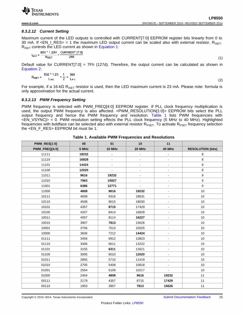
Table 1. Available PWM Frequencies and ResolutionsPWM_RES[1:0] 00 01 10 11
PWM_FREQ[4:0] 5 MHz 10 MHz 20 MHz 40 MHz RESOLUTION (bits)11111 19232 - - - 811110 16828 - - - 811101 14424 - - - 811100 12020 - - - 811011 9616 19232 - - 911010 7963 15927 - - 911001 6386 12771 - - 911000 4808 9616 19232 - 1010111 4658 9316 18631 - 1010110 4508 9015 18030 - 1010101 4357 8715 17429 - 1010100 4207 8414 16828 - 1010011 4057 8114 16227 - 1010010 3907 7813 15626 - 1010001 3756 7513 15025 - 1010000 3606 7212 14424 - 1001111 3456 6912 13823 - 1001110 3306 6611 13222 - 1001101 3155 6311 12621 - 1001100 3005 6010 12020 - 1001011 2855 5710 11419 - 1001010 2705 5409 10818 - 1001001 2554 5109 10217 - 1001000 2404 4808 9616 19232 1100111 2179 4357 8715 17429 1100110 1953 3907 7813 15626 11
Copyright © 2010–2014, Texas Instruments Incorporated Submit Documentation Feedback 15
Product Folder Links: LP8550
OUT1
OUT2
OUT3
OUT4
OUT5
OUT6
tSHIFT = 1/(FPWM x 6)Shift time
1/(FPWM)Cycle time
LP8550SNVS657E –SEPTEMBER 2010–REVISED SEPTEMBER 2014 www.ti.com
Table 1. Available PWM Frequencies and Resolutions (continued)PWM_RES[1:0] 00 01 10 11
PWM_FREQ[4:0] 5 MHz 10 MHz 20 MHz 40 MHz RESOLUTION (bits)00101 1728 3456 6912 13823 1100100 1503 3005 6010 12020 1100011 1202 2404 4808 9616 1200010 1052 2104 4207 8414 1200001 826 1653 3306 6611 1200000 601 1202 2404 4808 13
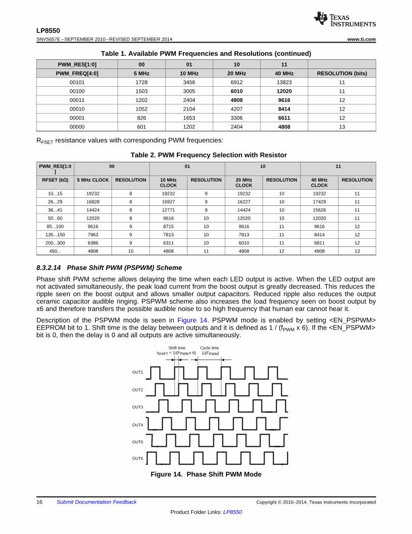
RFSET resistance values with corresponding PWM frequencies:
Table 2. PWM Frequency Selection with ResistorPWM_RES[1:0 00 01 10 11
]
RFSET (kΩ) 5 MHz CLOCK RESOLUTION 10 MHz RESOLUTION 20 MHz RESOLUTION 40 MHz RESOLUTIONCLOCK CLOCK CLOCK
10...15 19232 8 19232 9 19232 10 19232 11
26...29 16828 8 15927 9 16227 10 17429 11
36...41 14424 8 12771 9 14424 10 15626 11
50...60 12020 8 9616 10 12020 10 12020 11
85...100 9616 9 8715 10 9616 11 9616 12
135...150 7963 9 7813 10 7813 11 8414 12
200...300 6386 9 6311 10 6010 11 6811 12
450... 4808 10 4808 11 4808 12 4808 13
8.3.2.14 Phase Shift PWM (PSPWM) SchemePhase shift PWM scheme allows delaying the time when each LED output is active. When the LED output arenot activated simultaneously, the peak load current from the boost output is greatly decreased. This reduces theripple seen on the boost output and allows smaller output capacitors. Reduced ripple also reduces the outputceramic capacitor audible ringing. PSPWM scheme also increases the load frequency seen on boost output byx6 and therefore transfers the possible audible noise to so high frequency that human ear cannot hear it.
Description of the PSPWM mode is seen in Figure 14. PSPWM mode is enabled by setting <EN_PSPWM>EEPROM bit to 1. Shift time is the delay between outputs and it is defined as 1 / (fPWM x 6). If the <EN_PSPWM>bit is 0, then the delay is 0 and all outputs are active simultaneously.
Figure 14. Phase Shift PWM Mode
16 Submit Documentation Feedback Copyright © 2010–2014, Texas Instruments Incorporated
Product Folder Links: LP8550
+1 LSB
PWM value 510 (10-bit)
PWM value 510 1/2 (10-bit)
PWM value 511 (10-bit)
Brightness (PWM)
Time
Slope Time
Advanced slope
Brightness (PWM) Sloper Input
PWM Output
Time
Normal slopeSteady state without dithering
If dither is enabled it willbe used during transitionto enable smooth effect
LP8550www.ti.com SNVS657E –SEPTEMBER 2010–REVISED SEPTEMBER 2014
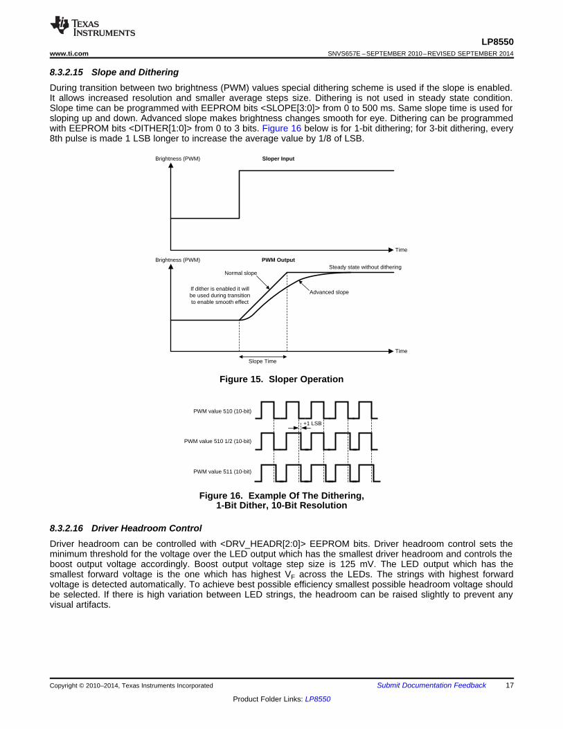
8.3.2.15 Slope and DitheringDuring transition between two brightness (PWM) values special dithering scheme is used if the slope is enabled.It allows increased resolution and smaller average steps size. Dithering is not used in steady state condition.Slope time can be programmed with EEPROM bits <SLOPE[3:0]> from 0 to 500 ms. Same slope time is used forsloping up and down. Advanced slope makes brightness changes smooth for eye. Dithering can be programmedwith EEPROM bits <DITHER[1:0]> from 0 to 3 bits. Figure 16 below is for 1-bit dithering; for 3-bit dithering, every8th pulse is made 1 LSB longer to increase the average value by 1/8 of LSB.
Figure 15. Sloper Operation
Figure 16. Example Of The Dithering,1-Bit Dither, 10-Bit Resolution
8.3.2.16 Driver Headroom ControlDriver headroom can be controlled with <DRV_HEADR[2:0]> EEPROM bits. Driver headroom control sets theminimum threshold for the voltage over the LED output which has the smallest driver headroom and controls theboost output voltage accordingly. Boost output voltage step size is 125 mV. The LED output which has thesmallest forward voltage is the one which has highest VF across the LEDs. The strings with highest forwardvoltage is detected automatically. To achieve best possible efficiency smallest possible headroom voltage shouldbe selected. If there is high variation between LED strings, the headroom can be raised slightly to prevent anyvisual artifacts.
Copyright © 2010–2014, Texas Instruments Incorporated Submit Documentation Feedback 17
Product Folder Links: LP8550

OVPLightLoad
SW
R R
OCP
SwitchDriver
R
S R
6+
-
+-
Osc/ramp
gm-
+VREF
FB
Boost output voltage
adjustment
Active Load
Startup
LP8550SNVS657E –SEPTEMBER 2010–REVISED SEPTEMBER 2014 www.ti.com
8.3.3 Boost Converter
8.3.3.1 OperationThe LP8550 boost DC/DC converter generates a 10-V to 40-V supply voltage for the LEDs from 2.7-V to 22-Vinput voltage. The output voltage can be controlled either with EEPROM register bits <VBOOST[4:0]> orautomatic adaptive voltage control can be used. The converter is a magnetic switching PWM mode DC/DCconverter with a current limit. The topology of the magnetic boost converter is called CPM (current programmedmode) control, where the inductor current is measured and controlled with the feedback. Switching frequency isselectable between 156 kHz and 1.25 MHz with EEPROM bit <BOOST_FREQ[1:0]>. When <EN_BOOST>EEPROM register bit is set to 1, then boost activates automatically when backlight is enabled.
In adaptive mode the boost output voltage is adjusted automatically based on LED driver headroom voltage.Boost output voltage control step size is in this case 125 mV to ensure as small as possible driver headroom andhigh efficiency. Enabling the adaptive mode is done with <EN_ADAPT> EEPROM bit. If boost is started withadaptive mode enabled, then the initial boost output voltage value is defined with the <VBOOST[4:0]> EEPROMregister bits in order to eliminate long output voltage iteration time when boost is started for the first time.Figure 17 shows the boost topology with the protection circuitry:
Figure 17. Boost Topology with Protection Circuitry
8.3.3.2 ProtectionThree different protection schemes are implemented:1. Overvoltage protection, limits the maximum output voltage.
– Overvoltage protection limit changes dynamically based on output voltage setting.– Keeps the output below breakdown voltage.– Prevents boost operation if battery voltage is much higher than desired output.
2. Overcurrent protection, limits the maximum inductor current.3. Duty cycle limiting.
8.3.3.3 Manual Output Voltage ControlUser can control the boost output voltage with <VBOOST[4:0]> EEPROM register bits when adaptive mode isdisabled.
VBOOST[4:0] VOLTAGE (typical)Bin Dec Volts
00000 0 1000001 1 1100010 2 1200011 3 1300100 4 14
18 Submit Documentation Feedback Copyright © 2010–2014, Texas Instruments Incorporated
Product Folder Links: LP8550
OU
T1
strin
g V
F
OU
T2
strin
g V
F
OU
T3
strin
g V
F
OU
T4
strin
g V
F
OU
T5
strin
g V
F
OU
T6
strin
g V
F
OU
T1
strin
g V
F
Time
VBOOST Driver headroom
VBOOST
LP8550www.ti.com SNVS657E –SEPTEMBER 2010–REVISED SEPTEMBER 2014
VBOOST[4:0] VOLTAGE (typical)... ... ...
11101 29 3911110 30 4011111 31 40
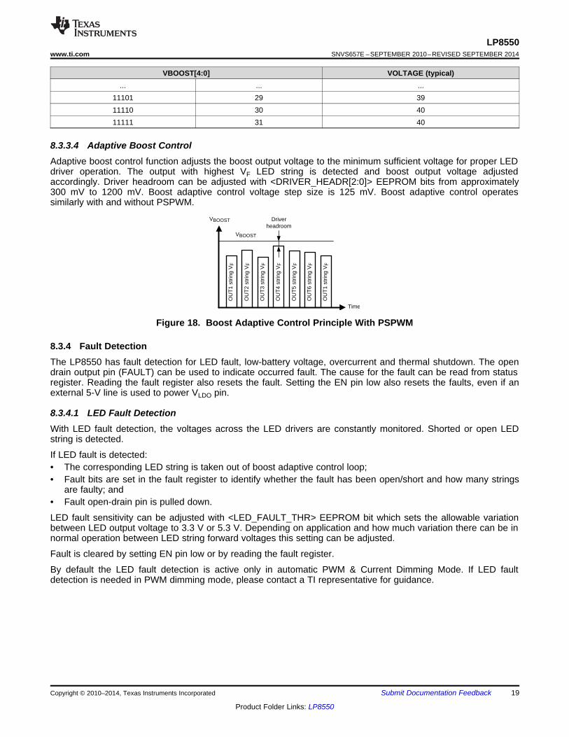
8.3.3.4 Adaptive Boost ControlAdaptive boost control function adjusts the boost output voltage to the minimum sufficient voltage for proper LEDdriver operation. The output with highest VF LED string is detected and boost output voltage adjustedaccordingly. Driver headroom can be adjusted with <DRIVER_HEADR[2:0]> EEPROM bits from approximately300 mV to 1200 mV. Boost adaptive control voltage step size is 125 mV. Boost adaptive control operatessimilarly with and without PSPWM.
Figure 18. Boost Adaptive Control Principle With PSPWM
8.3.4 Fault DetectionThe LP8550 has fault detection for LED fault, low-battery voltage, overcurrent and thermal shutdown. The opendrain output pin (FAULT) can be used to indicate occurred fault. The cause for the fault can be read from statusregister. Reading the fault register also resets the fault. Setting the EN pin low also resets the faults, even if anexternal 5-V line is used to power VLDO pin.
8.3.4.1 LED Fault DetectionWith LED fault detection, the voltages across the LED drivers are constantly monitored. Shorted or open LEDstring is detected.
If LED fault is detected:• The corresponding LED string is taken out of boost adaptive control loop;• Fault bits are set in the fault register to identify whether the fault has been open/short and how many strings
are faulty; and• Fault open-drain pin is pulled down.
LED fault sensitivity can be adjusted with <LED_FAULT_THR> EEPROM bit which sets the allowable variationbetween LED output voltage to 3.3 V or 5.3 V. Depending on application and how much variation there can be innormal operation between LED string forward voltages this setting can be adjusted.
Fault is cleared by setting EN pin low or by reading the fault register.
By default the LED fault detection is active only in automatic PWM & Current Dimming Mode. If LED faultdetection is needed in PWM dimming mode, please contact a TI representative for guidance.
Copyright © 2010–2014, Texas Instruments Incorporated Submit Documentation Feedback 19
Product Folder Links: LP8550
LP8550SNVS657E –SEPTEMBER 2010–REVISED SEPTEMBER 2014 www.ti.com
8.3.4.2 Undervoltage DetectionThe LP8550 has detection for too-low VIN voltage. Threshold level for the voltage is set with EEPROM registerbits as seen in Table 3:
Table 3. Threshold Level for Voltage Set with EEPROM Register BitsUVLO[1:0] THRESHOLD (V)
00 OFF01 2.710 5.411 8.1
When undervoltage is detected the LED outputs and boost shut down, FAULT pin is pulled down, andcorresponding fault bit is set in fault register. LEDs and boost start again when the voltage has increased abovethe threshold level. Hysteresis is implemented to threshold level to avoid continuous triggering of fault whenthreshold is reached.
Fault is cleared by setting EN pin low or by reading the fault register.
8.3.4.3 Overcurrent ProtectionThe LP8550 has detection for too-high loading on the boost converter. When overcurrent fault is detected, theLP8550 shuts down.
Fault is cleared by setting EN pin low or by reading the fault register.
8.3.4.4 Device Thermal RegulationThe LP8550 has an internal temperature sensor which can be used to measure the junction temperature of thedevice and protect the device from overheating. During thermal regulation, LED PWM is reduced by 2% of fullscale per °C whenever the temperature threshold is reached. Temperature regulation is enabled automaticallywhen chip is enabled. 11-bit temperature value can be read from Temp MSB and Temp LSB registers, MSBshould be read first. Temperature limit can be programmed in EEPROM as shown in Table 4.
Thermal regulation function does not generate fault signal.
Table 4. Temperature Limits Programmable in EEPROMTEMP_LIM[1:0] OVER-TEMP LIMIT (°C)
00 OFF01 11010 12011 130
8.3.4.5 Thermal ShutdownIf the LP8550 reaches thermal shutdown temperature (150°C ) the LED outputs and boost shuts down to protectit from damage. Also the FAULT pin is pulled down to indicate the fault state. The device activates again whentemperature drops below 130°C degrees.
Fault is cleared by setting EN pin low or by reading the fault register.
20 Submit Documentation Feedback Copyright © 2010–2014, Texas Instruments Incorporated
Product Folder Links: LP8550
STANDBY
RESET
INTERNALSTARTUP
SEQUENCE
EN = L (VLDO low)or POR = H
EN_BOOST = 1*
TSD = H
~2 ms Delay
BOOST STARTUP
EN = H (pin) and BL_CTL = 1 or PWM = H (pin)
BL_CTL = 0 and PWM = L
EN_BOOST = 0*
~4 ms Delay
NORMAL MODE
EN_BOOST
rising edge*
*) TSD = L
VREF = 95% OK*
EN = H (pin) VLDO ok
LP8550www.ti.com SNVS657E –SEPTEMBER 2010–REVISED SEPTEMBER 2014
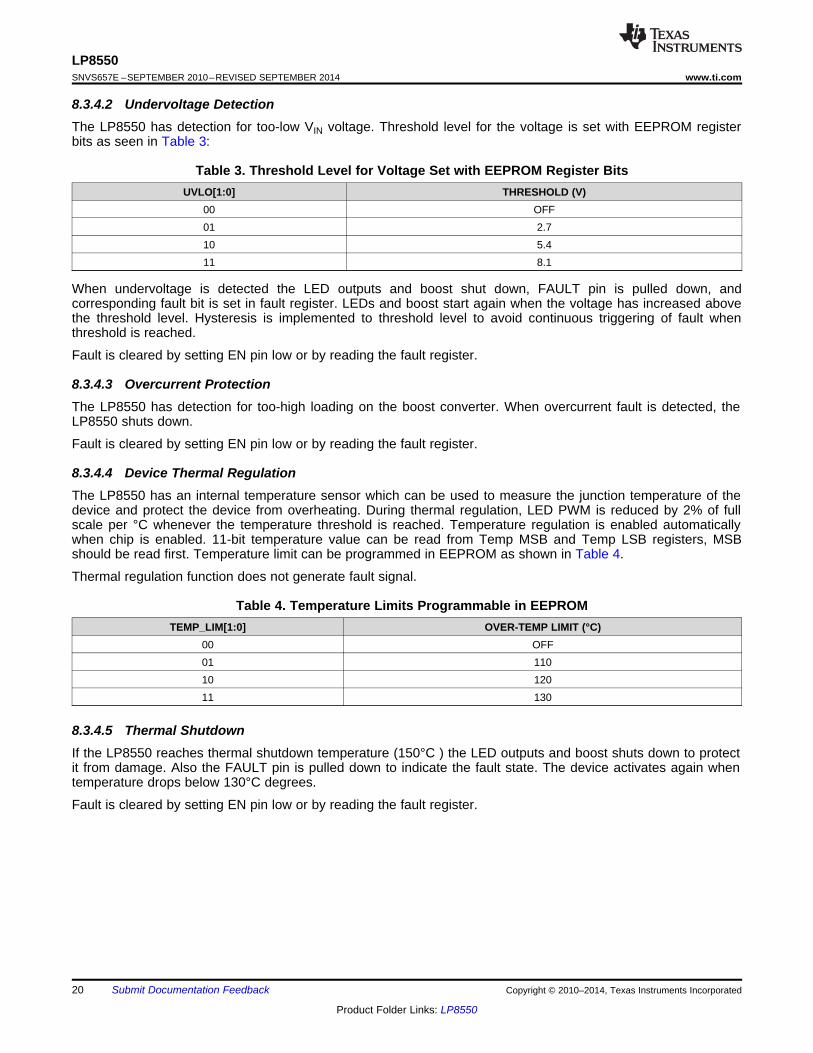
8.4 Device Functional Modes
Figure 19. Modes of Operation
RESET: In the RESET mode all the internal registers are reset to the default values. Reset is enteredalways when VLDO voltage is low. EN pin is enable for the internal LDO. Power On Reset (POR)activates during the chip startup or when the supply voltage VLDO falls below POR level. OnceVLDO rises above POR level, POR will inactivate, and the chip will continue to the STANDBYmode.
STANDBY: The STANDBY mode is entered if the register bit BL_CTL is LOW and external PWM input is notactive and POR is not active. This is the low power consumption mode, when only internal 5V LDOis enabled. Registers can be written in this mode, and the control bits are effective immediatelyafter start-up.
START-UP: When BL_CTL bit is written high or PWM signal is high, the INTERNAL START-UP SEQUENCEpowers up all the needed internal blocks (VREF, Bias, Oscillator etc.). Internal EPROM andEEPROM are read in this mode. To ensure the correct oscillator initialization, etc., a 2-ms delay isgenerated by the internal state-machine. If the chip temperature rises too high, the ThermalShutdown (TSD) disables the chip operation and STARTUP mode is entered until no thermalshutdown event is present.
BOOST START-UP: Soft start for boost output is generated in the BOOST START-UP mode. The boost outputis raised in low current PWM mode during the 4 ms delay generated by the state-machine. All LEDoutputs are off during the 4-ms delay to ensure smooth start-up. The Boost start-up is entered fromInternal Start-up Sequence if EN_BOOST is HIGH.
NORMAL: During NORMAL mode the user controls the chip using the external PWM input or with ControlRegisters through I2C. The registers can be written in any sequence and any number of bits can bealtered in a register in one write.
Copyright © 2010–2014, Texas Instruments Incorporated Submit Documentation Feedback 21
Product Folder Links: LP8550
SCL 21 873 - 6 9S
StartCondition
AcknowledgmentSignal From Receiver
Data Output by
Receiver
Data Output by
Transmitter
Transmitter Stays Off theBus During theAcknowledgment Clock
SDA
SCL
Data LineStable:Data Valid
Changeof DataAllowed
LP8550SNVS657E –SEPTEMBER 2010–REVISED SEPTEMBER 2014 www.ti.com
8.5 Programming
8.5.1 I2C-Compatible Serial Bus Interface
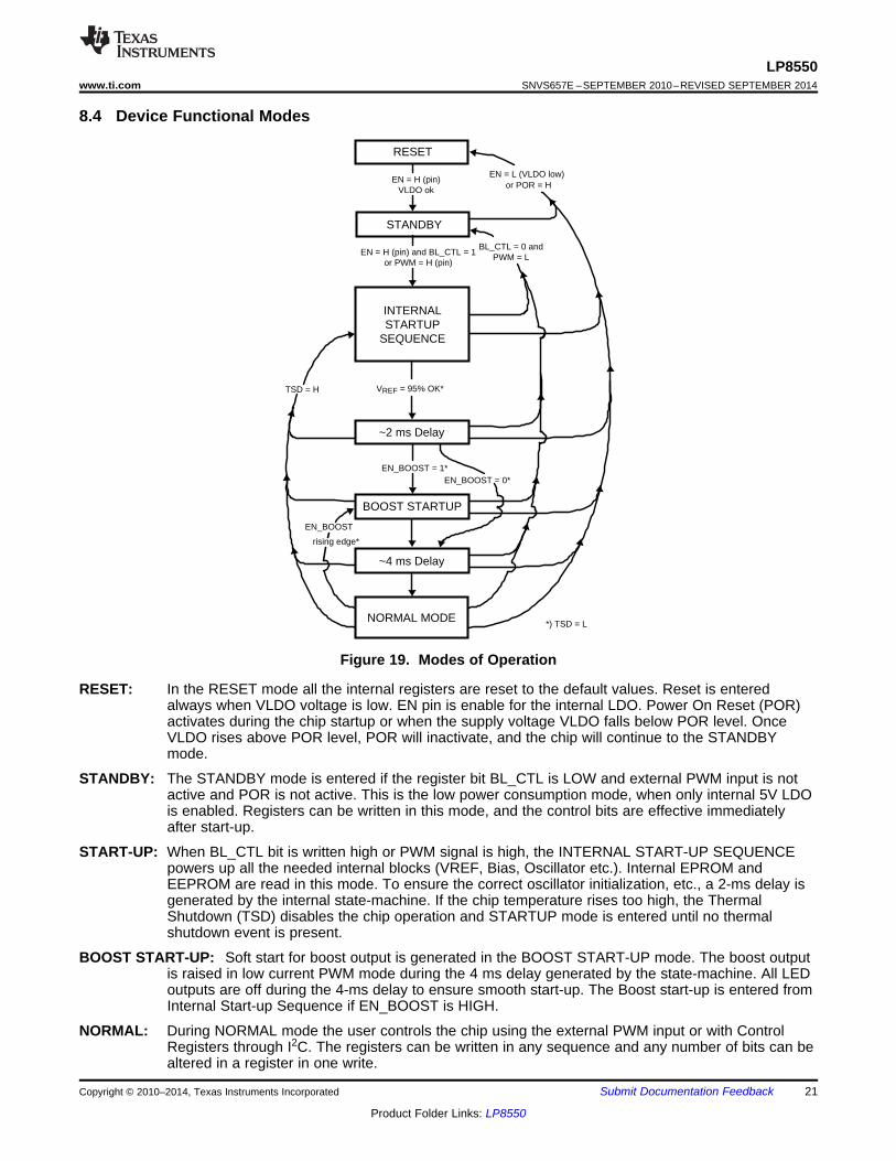
8.5.1.1 Interface Bus OverviewThe I2C-compatible synchronous serial interface provides access to the programmable functions and registers onthe device. This protocol uses a two-wire interface for bidirectional communications between the ICs connectedto the bus. The two interface lines are the Serial Data Line (SDA) and the Serial Clock Line (SCLK). These linesshould be connected to a positive supply, via a pull-up resistor and remain HIGH even when the bus is idle.
Every device on the bus is assigned a unique address and acts as either a Master or a Slave depending onwhether it generates or receives the SCLK. The LP8550 is always a slave device.
8.5.1.2 Data TransactionsOne data bit is transferred during each clock pulse. Data is sampled during the high state of the serial clockSCLK. Consequently, throughout the clock’s high period, the data should remain stable. Any changes on theSDA line during the high state of the SCLK and in the middle of a transaction, aborts the current transaction.New data should be sent during the low SCLK state. This protocol permits a single data line to transfer bothcommand/control information and data using the synchronous serial clock.
Figure 20. Bit Transfer
Each data transaction is composed of a Start Condition, a number of byte transfers (set by the software) and aStop Condition to terminate the transaction. Every byte written to the SDA bus must be 8 bits long and istransferred with the most significant bit first. After each byte, an Acknowledge signal must follow as described inbelow sections.
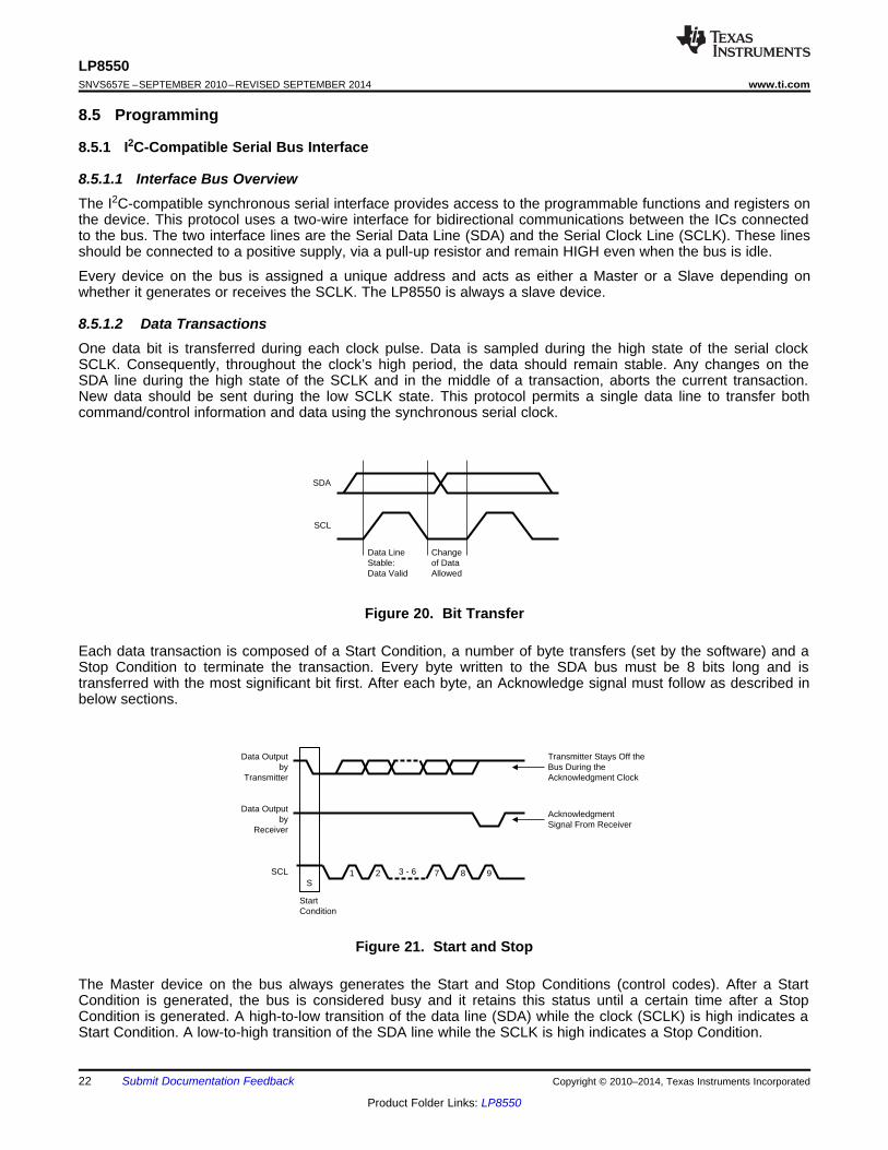
Figure 21. Start and Stop
The Master device on the bus always generates the Start and Stop Conditions (control codes). After a StartCondition is generated, the bus is considered busy and it retains this status until a certain time after a StopCondition is generated. A high-to-low transition of the data line (SDA) while the clock (SCLK) is high indicates aStart Condition. A low-to-high transition of the SDA line while the SCLK is high indicates a Stop Condition.
22 Submit Documentation Feedback Copyright © 2010–2014, Texas Instruments Incorporated
Product Folder Links: LP8550
ADR6Bit7
ADR5bit6
ADR4bit5
ADR3bit4
ADR2bit3
ADR1bit2
ADR0bit1
R/Wbit0
MSB LSB
x x x
I2C SLAVE address (chip address)
x x x x
SDA
SCL
StartCondition
StopCondition
S P
LP8550www.ti.com SNVS657E –SEPTEMBER 2010–REVISED SEPTEMBER 2014
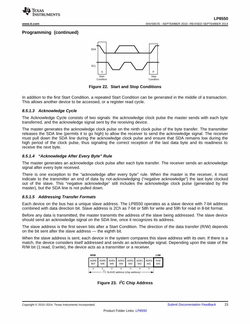
Programming (continued)
Figure 22. Start and Stop Conditions
In addition to the first Start Condition, a repeated Start Condition can be generated in the middle of a transaction.This allows another device to be accessed, or a register read cycle.
8.5.1.3 Acknowledge CycleThe Acknowledge Cycle consists of two signals: the acknowledge clock pulse the master sends with each bytetransferred, and the acknowledge signal sent by the receiving device.
The master generates the acknowledge clock pulse on the ninth clock pulse of the byte transfer. The transmitterreleases the SDA line (permits it to go high) to allow the receiver to send the acknowledge signal. The receivermust pull down the SDA line during the acknowledge clock pulse and ensure that SDA remains low during thehigh period of the clock pulse, thus signaling the correct reception of the last data byte and its readiness toreceive the next byte.
8.5.1.4 “Acknowledge After Every Byte” RuleThe master generates an acknowledge clock pulse after each byte transfer. The receiver sends an acknowledgesignal after every byte received.
There is one exception to the “acknowledge after every byte” rule. When the master is the receiver, it mustindicate to the transmitter an end of data by not-acknowledging (“negative acknowledge”) the last byte clockedout of the slave. This “negative acknowledge” still includes the acknowledge clock pulse (generated by themaster), but the SDA line is not pulled down.
8.5.1.5 Addressing Transfer FormatsEach device on the bus has a unique slave address. The LP8550 operates as a slave device with 7-bit addresscombined with data direction bit. Slave address is 2Ch as 7-bit or 58h for write and 59h for read in 8-bit format.
Before any data is transmitted, the master transmits the address of the slave being addressed. The slave deviceshould send an acknowledge signal on the SDA line, once it recognizes its address.
The slave address is the first seven bits after a Start Condition. The direction of the data transfer (R/W) dependson the bit sent after the slave address — the eighth bit.
When the slave address is sent, each device in the system compares this slave address with its own. If there is amatch, the device considers itself addressed and sends an acknowledge signal. Depending upon the state of theR/W bit (1:read, 0:write), the device acts as a transmitter or a receiver.
Figure 23. I2C Chip Address
Copyright © 2010–2014, Texas Instruments Incorporated Submit Documentation Feedback 23
Product Folder Links: LP8550
LP8550SNVS657E –SEPTEMBER 2010–REVISED SEPTEMBER 2014 www.ti.com
Programming (continued)8.5.1.6 Control Register Write Cycle• Master device generates start condition.• Master device sends slave address (7 bits) and the data direction bit (r/w = 0).• Slave device sends acknowledge signal if the slave address is correct.• Master sends control register address (8 bits).• Slave sends acknowledge signal.• Master sends data byte to be written to the addressed register.• Slave sends acknowledge signal.• If master will send further data bytes the control register address will be incremented by one after
acknowledge signal.• Write cycle ends when the master creates stop condition.
8.5.1.7 Control Register Read Cycle• Master device generates a start condition.• Master device sends slave address (7 bits) and the data direction bit (r/w = 0).• Slave device sends acknowledge signal if the slave address is correct.• Master sends control register address (8 bits).• Slave sends acknowledge signal.• Master device generates repeated start condition.• Master sends the slave address (7 bits) and the data direction bit (r/w = 1).• Slave sends acknowledge signal if the slave address is correct.• Slave sends data byte from addressed register.• If the master device sends acknowledge signal, the control register address will be incremented by one. Slave
device sends data byte from addressed register.• Read cycle ends when the master does not generate acknowledge signal after data byte and generates stop
condition.
Table 5. Data Read and Write CyclesADDRESS MODE<Start Condition><Slave Address><r/w = 0>[Ack]<Register Addr.>[Ack]<Repeated Start Condition>Data Read <Slave Address><r/w = 1>[Ack][Register Data]<Ack or NAck>… additional reads from subsequent register address possible<Stop Condition><Start Condition><Slave Address><r/w=’0’>[Ack]<Register Addr.>[Ack]Data Write <Register Data>[Ack]… additional writes to subsequent register address possible<Stop Condition>
24 Submit Documentation Feedback Copyright © 2010–2014, Texas Instruments Incorporated
Product Folder Links: LP8550

A/NA
S '0'Slave Address
(7 bits)Control Register Add.
(8 bits)A AData- Data
(8 bits) P
R/WData transfered, byte + Ack/NAck
SrSlave Address
(7 bits) '1' A
R/W
Direction of the transfer will change at this point
From Master to Slave
From Slave to Master A - ACKNOWLEDGE (SDA Low)
S - START CONDITION
P - STOP CONDITION
Sr - REPEATED START CONDITION
Register Read Format
NA - ACKNOWLEDGE (SDA High)
S '0'Slave Address
(7 bits)Control Register Add.
(8 bits)A A ARegister Data
(8 bits) P
R/W
From Master to Slave
From Slave to Master A - ACKNOWLEDGE (SDA Low)
S - START CONDITION
P - STOP CONDITION
Data transfered,byte + Ack
Register Write Format
LP8550www.ti.com SNVS657E –SEPTEMBER 2010–REVISED SEPTEMBER 2014
<>Data from master [ ] Data from slave
Figure 24. Register Write
Figure 25. Register Read
8.5.2 EEPROMEEPROM memory stores various parameters for chip control. The 64-bit EEPROM memory is organized as 8 x 8bits. The EEPROM structure consists of a register front-end and the non-volatile memory (NVM). Register datacan be read and written through the serial interface, and data is effective immediately. To read and programNVM, separate commands need to be sent. Erase and program voltages are generated on-chip charge pump, noother voltages than normal input voltage are required. A complete EEPROM memory map is shown in theEEPROM Register Map.
NOTEEEPROM NVM can be programmed or read by customer for bench validation.Programming for production devices should be done in TI production test, whereappropriate checks are performed to confirm EEPROM validity. Writing to EEPROMControl register of production devices (for burning or reading EEPROM) is notrecommended. If special EEPROM configuration is required, please contact the TI SalesOffice for availability.
Copyright © 2010–2014, Texas Instruments Incorporated Submit Documentation Feedback 25
Product Folder Links: LP8550

EEPROMNVM
8 x 8 bits
REGISTERSADDRESS 00h...72h
Startup orEE_READ=1
User
Device Control
I2 C
EEPROM REGISTERS
Address A0h...A7h
EE_PROG = 1
Device Control
LP8550SNVS657E –SEPTEMBER 2010–REVISED SEPTEMBER 2014 www.ti.com
Figure 26. EEPROM Control Structure
8.6 Register Maps
Table 6. Register MapADDR REGISTER D7 D6 D5 D4 D3 D2 D1 D0 DEFAULT
00H Brightness Control BRT[7:0] 0000 0000
01H Device Control BRT_MODE[1:0] BL_CTL 0000 0000
02H Fault OPEN SHORT 2_CHANNELS 1_CHANNEL BL_FAULT OCP TSD UVLO 0000 0000
03H ID PANEL MFG[3:0] REV[2:0] 1111 1100
04H Direct Control OUT[6:1] 0000 0000
05H Temp MSB TEMP[10:3] 0000 0000
06H Temp LSB TEMP[2:0] 0000 0000
72H EEPROM_control EE_READY EE_INIT EE_PROG EE_READ 0000 0000
8.6.1 Register Bit Explanations
8.6.1.1 Brightness ControlAddress 00h
Reset value 0000 0000b
BRIGHTNESS CONTROL REGISTER7 6 5 4 3 2 1 0
BRT[7:0]Name Bit Access DescriptionBRT 7:0 R/W Backlight PWM 8-bit linear control.
8.6.1.2 Device ControlAddress 01h
Reset value 0000 0000b
DEVICE CONTROL REGISTER7 6 5 4 3 2 1 0
BRT_MODE[1:0] BL_CTLName Bit Access Description
26 Submit Documentation Feedback Copyright © 2010–2014, Texas Instruments Incorporated
Product Folder Links: LP8550
LP8550www.ti.com SNVS657E –SEPTEMBER 2010–REVISED SEPTEMBER 2014
DEVICE CONTROL REGISTERBRT_MODE 2:1 R/W PWM source mode
00b = PWM input pin duty cycle control (default)01b = PWM input pin duty cycle control10b = Brightness register11b = Direct PWM control from PWM input pin
BL_CTL 0 R/W Enable backlight0 = Backlight disabled and chip turned off if BRT_MODE[1:0] = 10. In external PWMpin control the state of the chip is defined with the PWM pin and this bit has noeffect.1 = Backlight enabled and chip turned on if BRT_MODE[1:0] = 10. In external PWMpin control the state of the chip is defined with the PWM pin and this bit has noeffect.
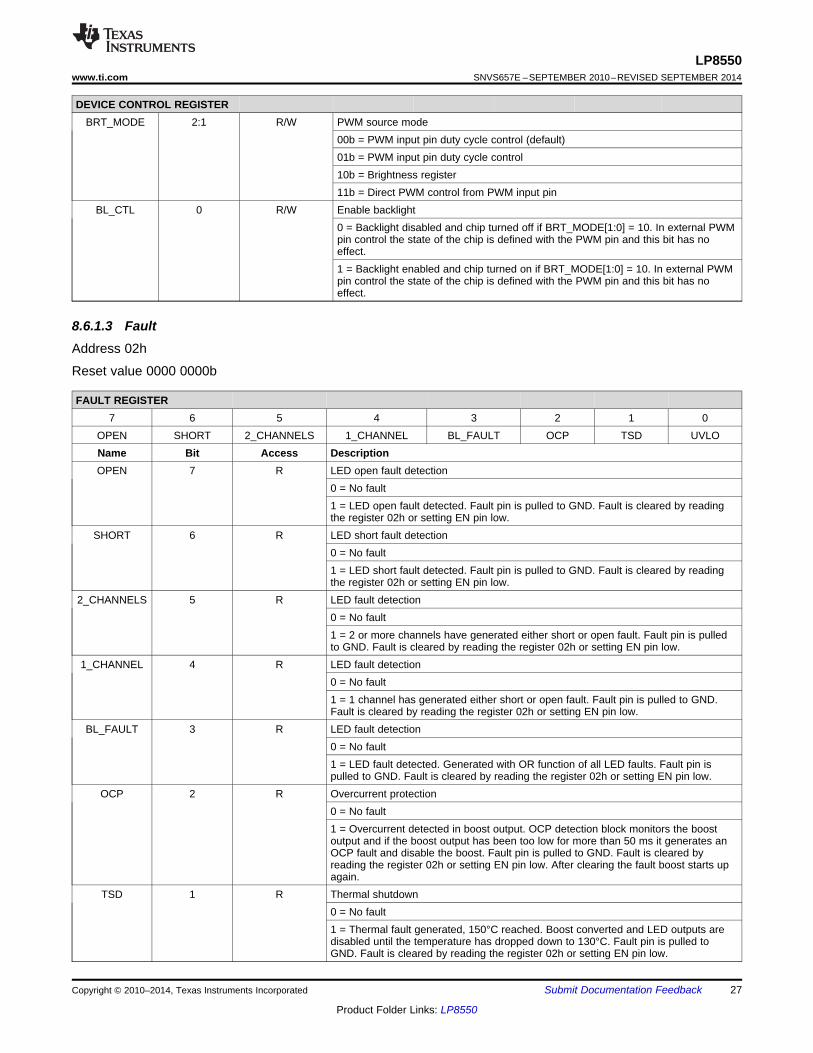
8.6.1.3 FaultAddress 02h
Reset value 0000 0000b
FAULT REGISTER7 6 5 4 3 2 1 0
OPEN SHORT 2_CHANNELS 1_CHANNEL BL_FAULT OCP TSD UVLOName Bit Access DescriptionOPEN 7 R LED open fault detection
0 = No fault1 = LED open fault detected. Fault pin is pulled to GND. Fault is cleared by readingthe register 02h or setting EN pin low.
SHORT 6 R LED short fault detection0 = No fault1 = LED short fault detected. Fault pin is pulled to GND. Fault is cleared by readingthe register 02h or setting EN pin low.
2_CHANNELS 5 R LED fault detection0 = No fault1 = 2 or more channels have generated either short or open fault. Fault pin is pulledto GND. Fault is cleared by reading the register 02h or setting EN pin low.
1_CHANNEL 4 R LED fault detection0 = No fault1 = 1 channel has generated either short or open fault. Fault pin is pulled to GND.Fault is cleared by reading the register 02h or setting EN pin low.
BL_FAULT 3 R LED fault detection0 = No fault1 = LED fault detected. Generated with OR function of all LED faults. Fault pin ispulled to GND. Fault is cleared by reading the register 02h or setting EN pin low.
OCP 2 R Overcurrent protection0 = No fault1 = Overcurrent detected in boost output. OCP detection block monitors the boostoutput and if the boost output has been too low for more than 50 ms it generates anOCP fault and disable the boost. Fault pin is pulled to GND. Fault is cleared byreading the register 02h or setting EN pin low. After clearing the fault boost starts upagain.
TSD 1 R Thermal shutdown0 = No fault1 = Thermal fault generated, 150°C reached. Boost converted and LED outputs aredisabled until the temperature has dropped down to 130°C. Fault pin is pulled toGND. Fault is cleared by reading the register 02h or setting EN pin low.
Copyright © 2010–2014, Texas Instruments Incorporated Submit Documentation Feedback 27
Product Folder Links: LP8550
LP8550SNVS657E –SEPTEMBER 2010–REVISED SEPTEMBER 2014 www.ti.com
FAULT REGISTERUVLO 0 R Undervoltage detection
0 = No fault1 = Undervoltage detected in VIN pin. Boost converted and LED outputs are disableduntil VIN voltage is above the threshold voltage. Threshold voltage is set withEEPROM bits from 3 V to 9 V. Fault pin is pulled to GND. Fault is cleared by readingthe register 02h or setting EN pin low.
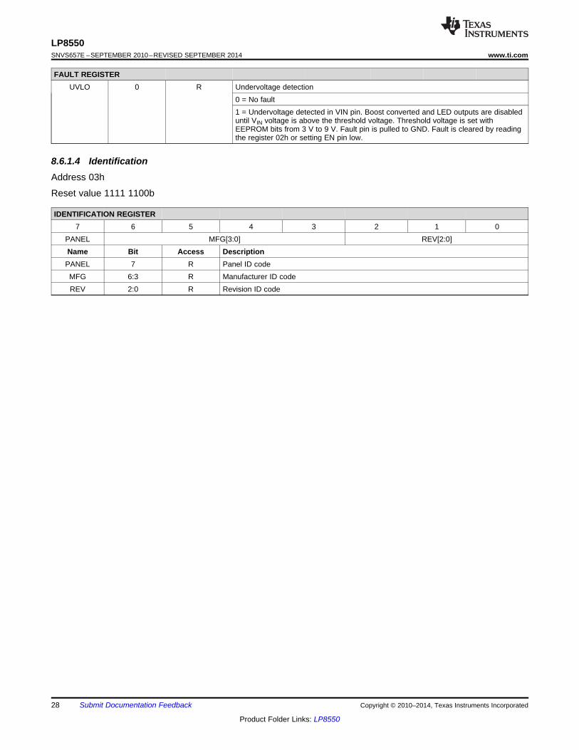
8.6.1.4 IdentificationAddress 03h
Reset value 1111 1100b
IDENTIFICATION REGISTER7 6 5 4 3 2 1 0
PANEL MFG[3:0] REV[2:0]Name Bit Access Description
PANEL 7 R Panel ID codeMFG 6:3 R Manufacturer ID codeREV 2:0 R Revision ID code
28 Submit Documentation Feedback Copyright © 2010–2014, Texas Instruments Incorporated
Product Folder Links: LP8550
LP8550www.ti.com SNVS657E –SEPTEMBER 2010–REVISED SEPTEMBER 2014
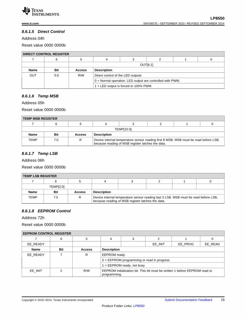
8.6.1.5 Direct ControlAddress 04h
Reset value 0000 0000b
DIRECT CONTROL REGISTER7 6 5 4 3 2 1 0
OUT[6:1]Name Bit Access DescriptionOUT 5:0 R/W Direct control of the LED outputs
0 = Normal operation. LED output are controlled with PWM.1 = LED output is forced to 100% PWM.
8.6.1.6 Temp MSBAddress 05h
Reset value 0000 0000b
TEMP MSB REGISTER7 6 5 4 3 2 1 0
TEMP[10:3]Name Bit Access DescriptionTEMP 7:0 R Device internal temperature sensor reading first 8 MSB. MSB must be read before LSB,
because reading of MSB register latches the data.
8.6.1.7 Temp LSBAddress 06h
Reset value 0000 0000b
TEMP LSB REGISTER7 6 5 4 3 2 1 0
TEMP[2:0]Name Bit Access DescriptionTEMP 7:5 R Device internal temperature sensor reading last 3 LSB. MSB must be read before LSB,
because reading of MSB register latches the data.
8.6.1.8 EEPROM ControlAddress 72h
Reset value 0000 0000b
EEPROM CONTROL REGISTER7 6 5 4 3 2 1 0
EE_READY EE_INIT EE_PROG EE_READName Bit Access Description
EE_READY 7 R EEPROM ready0 = EEPROM programming or read in progress1 = EEPROM ready, not busy
EE_INIT 2 R/W EEPROM initialization bit. This bit must be written 1 before EEPROM read orprogramming.
Copyright © 2010–2014, Texas Instruments Incorporated Submit Documentation Feedback 29
Product Folder Links: LP8550
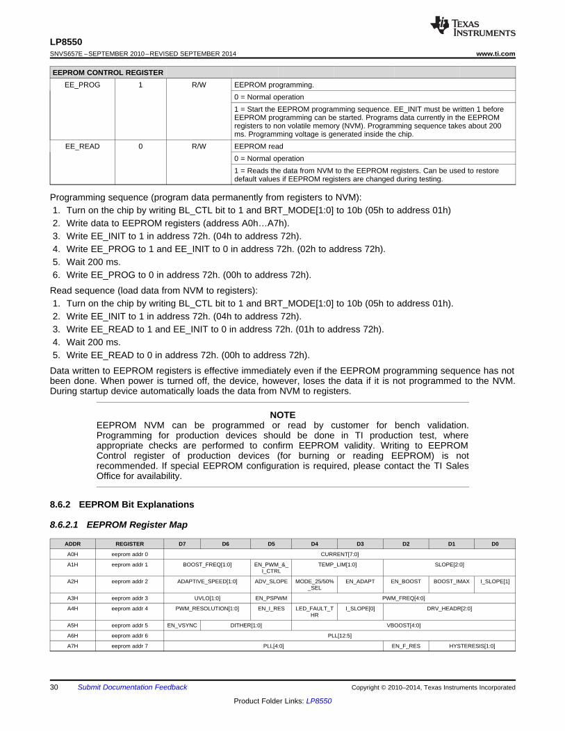
LP8550SNVS657E –SEPTEMBER 2010–REVISED SEPTEMBER 2014 www.ti.com
EEPROM CONTROL REGISTEREE_PROG 1 R/W EEPROM programming.
0 = Normal operation1 = Start the EEPROM programming sequence. EE_INIT must be written 1 beforeEEPROM programming can be started. Programs data currently in the EEPROMregisters to non volatile memory (NVM). Programming sequence takes about 200ms. Programming voltage is generated inside the chip.
EE_READ 0 R/W EEPROM read0 = Normal operation1 = Reads the data from NVM to the EEPROM registers. Can be used to restoredefault values if EEPROM registers are changed during testing.
Programming sequence (program data permanently from registers to NVM):1. Turn on the chip by writing BL_CTL bit to 1 and BRT_MODE[1:0] to 10b (05h to address 01h)2. Write data to EEPROM registers (address A0h…A7h).3. Write EE_INIT to 1 in address 72h. (04h to address 72h).4. Write EE_PROG to 1 and EE_INIT to 0 in address 72h. (02h to address 72h).5. Wait 200 ms.6. Write EE_PROG to 0 in address 72h. (00h to address 72h).
Read sequence (load data from NVM to registers):1. Turn on the chip by writing BL_CTL bit to 1 and BRT_MODE[1:0] to 10b (05h to address 01h).2. Write EE_INIT to 1 in address 72h. (04h to address 72h).3. Write EE_READ to 1 and EE_INIT to 0 in address 72h. (01h to address 72h).4. Wait 200 ms.5. Write EE_READ to 0 in address 72h. (00h to address 72h).
Data written to EEPROM registers is effective immediately even if the EEPROM programming sequence has notbeen done. When power is turned off, the device, however, loses the data if it is not programmed to the NVM.During startup device automatically loads the data from NVM to registers.
NOTEEEPROM NVM can be programmed or read by customer for bench validation.Programming for production devices should be done in TI production test, whereappropriate checks are performed to confirm EEPROM validity. Writing to EEPROMControl register of production devices (for burning or reading EEPROM) is notrecommended. If special EEPROM configuration is required, please contact the TI SalesOffice for availability.
8.6.2 EEPROM Bit Explanations
8.6.2.1 EEPROM Register Map
ADDR REGISTER D7 D6 D5 D4 D3 D2 D1 D0
A0H eeprom addr 0 CURRENT[7:0]
A1H eeprom addr 1 BOOST_FREQ[1:0] EN_PWM_&_ TEMP_LIM[1:0] SLOPE[2:0]I_CTRL
A2H eeprom addr 2 ADAPTIVE_SPEED[1:0] ADV_SLOPE MODE_25/50% EN_ADAPT EN_BOOST BOOST_IMAX I_SLOPE[1]_SEL
A3H eeprom addr 3 UVLO[1:0] EN_PSPWM PWM_FREQ[4:0]
A4H eeprom addr 4 PWM_RESOLUTION[1:0] EN_I_RES LED_FAULT_T I_SLOPE[0] DRV_HEADR[2:0]HR
A5H eeprom addr 5 EN_VSYNC DITHER[1:0] VBOOST[4:0]
A6H eeprom addr 6 PLL[12:5]
A7H eeprom addr 7 PLL[4:0] EN_F_RES HYSTERESIS[1:0]
30 Submit Documentation Feedback Copyright © 2010–2014, Texas Instruments Incorporated
Product Folder Links: LP8550
LP8550www.ti.com SNVS657E –SEPTEMBER 2010–REVISED SEPTEMBER 2014
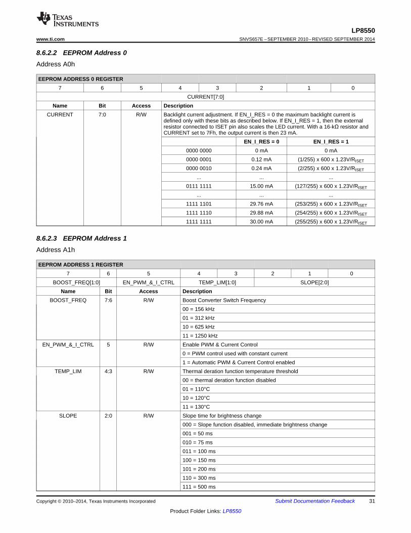
8.6.2.2 EEPROM Address 0Address A0h
EEPROM ADDRESS 0 REGISTER7 6 5 4 3 2 1 0
CURRENT[7:0]Name Bit Access Description
CURRENT 7:0 R/W Backlight current adjustment. If EN_I_RES = 0 the maximum backlight current isdefined only with these bits as described below. If EN_I_RES = 1, then the externalresistor connected to ISET pin also scales the LED current. With a 16-kΩ resistor andCURRENT set to 7Fh, the output current is then 23 mA.
EN_I_RES = 0 EN_I_RES = 10000 0000 0 mA 0 mA0000 0001 0.12 mA (1/255) x 600 x 1.23V/RISET
0000 0010 0.24 mA (2/255) x 600 x 1.23V/RISET
... ... ...0111 1111 15.00 mA (127/255) x 600 x 1.23V/RISET
... ... ...1111 1101 29.76 mA (253/255) x 600 x 1.23V/RISET
1111 1110 29.88 mA (254/255) x 600 x 1.23V/RISET
1111 1111 30.00 mA (255/255) x 600 x 1.23V/RISET
8.6.2.3 EEPROM Address 1Address A1h
EEPROM ADDRESS 1 REGISTER7 6 5 4 3 2 1 0
BOOST_FREQ[1:0] EN_PWM_&_I_CTRL TEMP_LIM[1:0] SLOPE[2:0]Name Bit Access Description
BOOST_FREQ 7:6 R/W Boost Converter Switch Frequency00 = 156 kHz01 = 312 kHz10 = 625 kHz11 = 1250 kHz
EN_PWM_&_I_CTRL 5 R/W Enable PWM & Current Control0 = PWM control used with constant current1 = Automatic PWM & Current Control enabled
TEMP_LIM 4:3 R/W Thermal deration function temperature threshold00 = thermal deration function disabled01 = 110°C10 = 120°C11 = 130°C
SLOPE 2:0 R/W Slope time for brightness change000 = Slope function disabled, immediate brightness change001 = 50 ms010 = 75 ms011 = 100 ms100 = 150 ms101 = 200 ms110 = 300 ms111 = 500 ms
Copyright © 2010–2014, Texas Instruments Incorporated Submit Documentation Feedback 31
Product Folder Links: LP8550
LP8550SNVS657E –SEPTEMBER 2010–REVISED SEPTEMBER 2014 www.ti.com
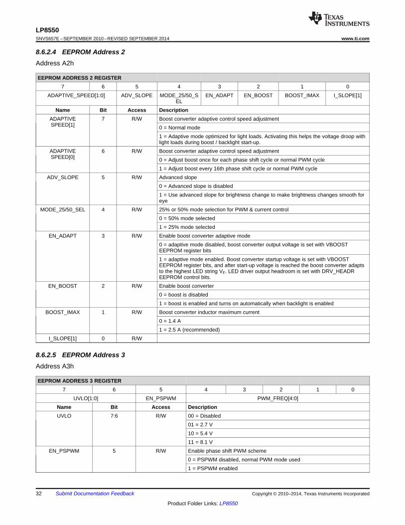
8.6.2.4 EEPROM Address 2Address A2h
EEPROM ADDRESS 2 REGISTER7 6 5 4 3 2 1 0
ADAPTIVE_SPEED[1:0] ADV_SLOPE MODE_25/50_S EN_ADAPT EN_BOOST BOOST_IMAX I_SLOPE[1]EL
Name Bit Access DescriptionADAPTIVE 7 R/W Boost converter adaptive control speed adjustmentSPEED[1] 0 = Normal mode
1 = Adaptive mode optimized for light loads. Activating this helps the voltage droop withlight loads during boost / backlight start-up.
ADAPTIVE 6 R/W Boost converter adaptive control speed adjustmentSPEED[0] 0 = Adjust boost once for each phase shift cycle or normal PWM cycle
1 = Adjust boost every 16th phase shift cycle or normal PWM cycleADV_SLOPE 5 R/W Advanced slope
0 = Advanced slope is disabled1 = Use advanced slope for brightness change to make brightness changes smooth foreye
MODE_25/50_SEL 4 R/W 25% or 50% mode selection for PWM & current control0 = 50% mode selected1 = 25% mode selected
EN_ADAPT 3 R/W Enable boost converter adaptive mode0 = adaptive mode disabled, boost converter output voltage is set with VBOOSTEEPROM register bits1 = adaptive mode enabled. Boost converter startup voltage is set with VBOOSTEEPROM register bits, and after start-up voltage is reached the boost converter adaptsto the highest LED string VF. LED driver output headroom is set with DRV_HEADREEPROM control bits.
EN_BOOST 2 R/W Enable boost converter0 = boost is disabled1 = boost is enabled and turns on automatically when backlight is enabled
BOOST_IMAX 1 R/W Boost converter inductor maximum current0 = 1.4 A1 = 2.5 A (recommended)
I_SLOPE[1] 0 R/W
8.6.2.5 EEPROM Address 3Address A3h
EEPROM ADDRESS 3 REGISTER7 6 5 4 3 2 1 0
UVLO[1:0] EN_PSPWM PWM_FREQ[4:0]Name Bit Access DescriptionUVLO 7:6 R/W 00 = Disabled
01 = 2.7 V10 = 5.4 V11 = 8.1 V
EN_PSPWM 5 R/W Enable phase shift PWM scheme0 = PSPWM disabled, normal PWM mode used1 = PSPWM enabled
32 Submit Documentation Feedback Copyright © 2010–2014, Texas Instruments Incorporated
Product Folder Links: LP8550
LP8550www.ti.com SNVS657E –SEPTEMBER 2010–REVISED SEPTEMBER 2014
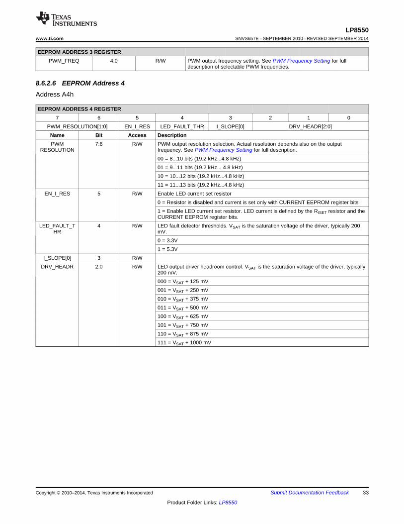
EEPROM ADDRESS 3 REGISTERPWM_FREQ 4:0 R/W PWM output frequency setting. See PWM Frequency Setting for full
description of selectable PWM frequencies.
8.6.2.6 EEPROM Address 4Address A4h
EEPROM ADDRESS 4 REGISTER7 6 5 4 3 2 1 0
PWM_RESOLUTION[1:0] EN_I_RES LED_FAULT_THR I_SLOPE[0] DRV_HEADR[2:0]Name Bit Access DescriptionPWM 7:6 R/W PWM output resolution selection. Actual resolution depends also on the output
RESOLUTION frequency. See PWM Frequency Setting for full description.00 = 8...10 bits (19.2 kHz...4.8 kHz)01 = 9...11 bits (19.2 kHz... 4.8 kHz)10 = 10...12 bits (19.2 kHz...4.8 kHz)11 = 11...13 bits (19.2 kHz...4.8 kHz)
EN_I_RES 5 R/W Enable LED current set resistor0 = Resistor is disabled and current is set only with CURRENT EEPROM register bits1 = Enable LED current set resistor. LED current is defined by the RISET resistor and theCURRENT EEPROM register bits.
LED_FAULT_T 4 R/W LED fault detector thresholds. VSAT is the saturation voltage of the driver, typically 200HR mV.
0 = 3.3V1 = 5.3V
I_SLOPE[0] 3 R/WDRV_HEADR 2:0 R/W LED output driver headroom control. VSAT is the saturation voltage of the driver, typically
200 mV.000 = VSAT + 125 mV001 = VSAT + 250 mV010 = VSAT + 375 mV011 = VSAT + 500 mV100 = VSAT + 625 mV101 = VSAT + 750 mV110 = VSAT + 875 mV111 = VSAT + 1000 mV
Copyright © 2010–2014, Texas Instruments Incorporated Submit Documentation Feedback 33
Product Folder Links: LP8550
LP8550SNVS657E –SEPTEMBER 2010–REVISED SEPTEMBER 2014 www.ti.com
8.6.2.7 EEPROM Address 5Address A5h
EEPROM ADDRESS 5 REGISTER7 6 5 4 3 2 1 0
EN_VSYNC DITHER[1:0] VBOOST[4:0]Name Bit Access Description
EN_VSYNC 7 R/W Enable VSYNC function0 = VSYNC input disabled1 = VSYNC input enabled. VSYNC signal is used by the internal PLL to generatePWM output and boost frequency.
DITHER 6:5 R/W Dither function controls00 = Dither function disabled01 = 1-bit dither used for output PWM transitions10 = 2-bit dither used for output PWM transitions11 = 3-bit dither used for output PWM transitions
VBOOST 4:0 R/W Boost voltage control from 10 V to 40 V with 1-V step. If adaptive boost control isenabled, this sets the initial start voltage for the boost converter. If adaptive modeis disabled, the output voltage of the boost converter is directly set.0 0000 = 10 V0 0001 = 11 V0 0010 = 12 V...1 1101 = 39 V1 1110 = 40 V1 1111 = 40 V
8.6.2.8 EEPROM Address 6Address A6h
EEPROM ADDRESS 6 register7 6 5 4 3 2 1 0
PLL[12:5]Name Bit Access DescriptionPLL 7:0 R/W 13-bit counter value for PLL, 8 MSB bits. PLL[12:0] bits are used when en_vsync =
1. See Table 7 for PLL value calculation.
8.6.2.9 EEPROM Address 7Address A7h
EEPROM ADDRESS 7 REGISTER7 6 5 4 3 2 1 0
PLL[4:0] EN_F_RES HYSTERESIS[1:0]Name Bit Access DescriptionPLL 7:3 R/W 13-bit counter value for PLL, 5 LSB bits. PLL[12:0] bits are used when en_vsync = 1. See
Table 7 for PLL value calculation.EN_F_RES 2 R/W Enable PWM output frequency set resistor
0 = Resistor is disabled and PWM output frequency is set with PWM_FREQ EEPROMregister bits1 = PWM frequency set resistor is enabled. RFSET defines the output PWM frequency. SeePWM Frequency Setting for full description of the PWM frequencies.
34 Submit Documentation Feedback Copyright © 2010–2014, Texas Instruments Incorporated
Product Folder Links: LP8550
LP8550www.ti.com SNVS657E –SEPTEMBER 2010–REVISED SEPTEMBER 2014
EEPROM ADDRESS 7 REGISTERHYSTERESIS 1:0 R/W PWM input hysteresis function. Defines how small changes in the PWM input are ignored to
remove constant switching between two values.00 = OFF01 = 1-bit hysteresis with 11-bit resolution10 = 1-bit hysteresis with 10-bit resolution11 = 1-bit hysteresis with 8-bit resolution
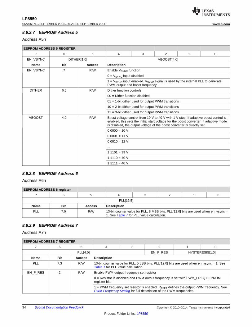
Table 7. PLL Value Calculationen_vsync PLL FREQUENCY [MHz] PLL[12:0]
0 5, 10, 20, 40 not used5 5 MHz / (26 x fVSYNC)10 10 MHz / (50 x fVSYNC)
120 20 MHz / (98 x fVSYNC)40 40 MHz / (196 x fVSYNC)
PLL frequency is set by PWM_RESOLUTION[1:0] bits.
For Example:
If fPLL = 5 MHz and fVSYNC = 60 Hz, then PLL[12:0] = 5000000 Hz / (26 * 60 Hz) = 3205d = C85h.
If fPLL = 10 MHz and fVSYNC = 75 Hz, then PLL[12:0] = 10000000 Hz / (50 * 75 Hz) = 2667d = A6Bh.
Copyright © 2010–2014, Texas Instruments Incorporated Submit Documentation Feedback 35
Product Folder Links: LP8550
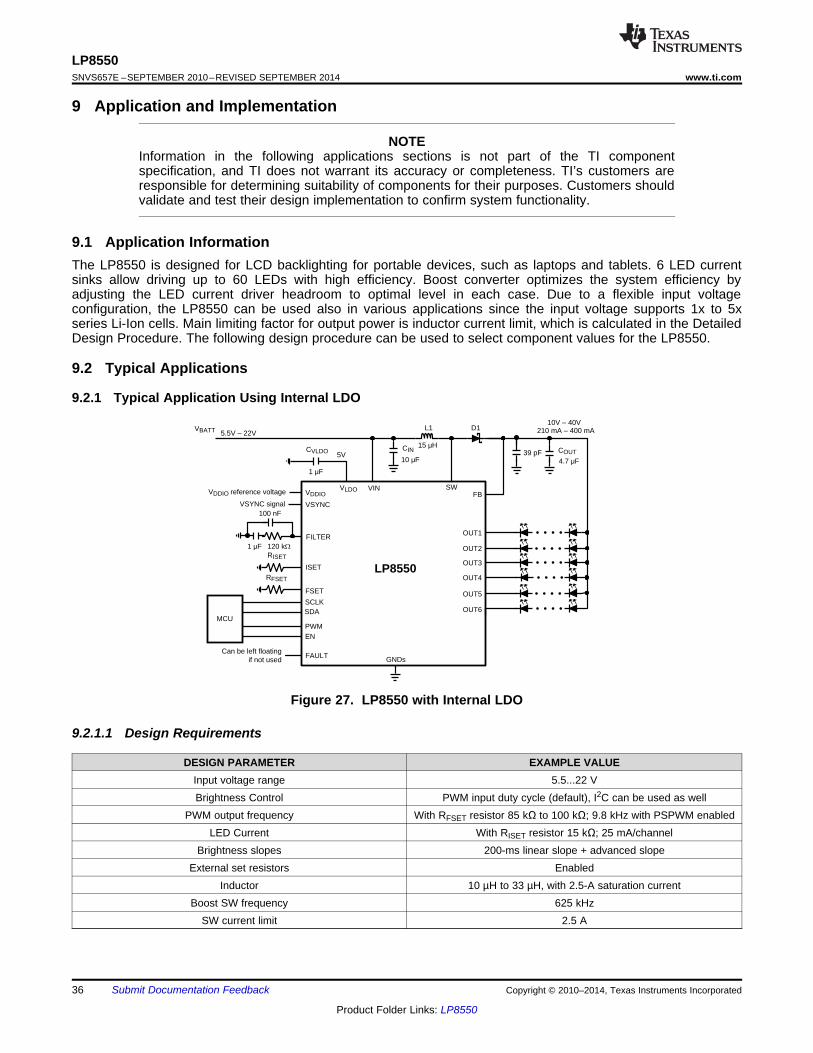
MCU
LP8550
SWFB
VLDO
GNDs
EN
ISET
VDDIO
PWM
SCLKSDA
OUT1
OUT2
OUT3
OUT4
OUT5
OUT6
L1 D110V ± 40V
5.5V ± 22V
FILTER
5V
FSET
15 éH
VSYNC
210 mA ± 400 mA
COUTCIN
10 éF 4.7 éF
CVLDO
1 éF
VDDIO reference voltage
VSYNC signal
120 k5
100 nF
1 éF
FAULTCan be left floating
if not used
39 pF
VIN
RISET
RFSET
VBATT
LP8550SNVS657E –SEPTEMBER 2010–REVISED SEPTEMBER 2014 www.ti.com
9 Application and Implementation
NOTEInformation in the following applications sections is not part of the TI componentspecification, and TI does not warrant its accuracy or completeness. TI’s customers areresponsible for determining suitability of components for their purposes. Customers shouldvalidate and test their design implementation to confirm system functionality.
9.1 Application InformationThe LP8550 is designed for LCD backlighting for portable devices, such as laptops and tablets. 6 LED currentsinks allow driving up to 60 LEDs with high efficiency. Boost converter optimizes the system efficiency byadjusting the LED current driver headroom to optimal level in each case. Due to a flexible input voltageconfiguration, the LP8550 can be used also in various applications since the input voltage supports 1x to 5xseries Li-Ion cells. Main limiting factor for output power is inductor current limit, which is calculated in the DetailedDesign Procedure. The following design procedure can be used to select component values for the LP8550.
9.2 Typical Applications
9.2.1 Typical Application Using Internal LDO
Figure 27. LP8550 with Internal LDO
9.2.1.1 Design Requirements
DESIGN PARAMETER EXAMPLE VALUEInput voltage range 5.5...22 VBrightness Control PWM input duty cycle (default), I2C can be used as well
PWM output frequency With RFSET resistor 85 kΩ to 100 kΩ; 9.8 kHz with PSPWM enabledLED Current With RISET resistor 15 kΩ; 25 mA/channel
Brightness slopes 200-ms linear slope + advanced slopeExternal set resistors Enabled
Inductor 10 µH to 33 µH, with 2.5-A saturation currentBoost SW frequency 625 kHz
SW current limit 2.5 A
36 Submit Documentation Feedback Copyright © 2010–2014, Texas Instruments Incorporated
Product Folder Links: LP8550
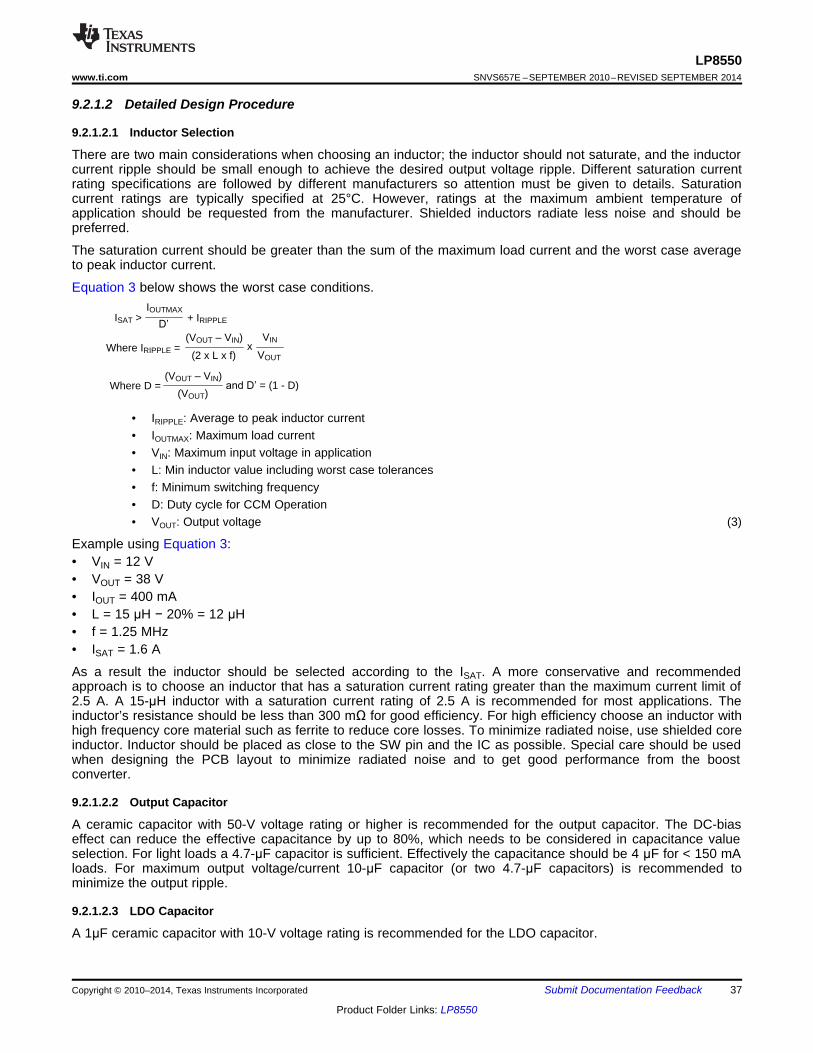
ISAT >
x(VOUT ± VIN)
VOUT
VIN
Where D =
Where IRIPPLE = (2 x L x f)
DQG'¶= (1 - D)(VOUT ± VIN)
(VOUT)
+ IRIPPLE
IOUTMAX
'
LP8550www.ti.com SNVS657E –SEPTEMBER 2010–REVISED SEPTEMBER 2014
9.2.1.2 Detailed Design Procedure
9.2.1.2.1 Inductor Selection
There are two main considerations when choosing an inductor; the inductor should not saturate, and the inductorcurrent ripple should be small enough to achieve the desired output voltage ripple. Different saturation currentrating specifications are followed by different manufacturers so attention must be given to details. Saturationcurrent ratings are typically specified at 25°C. However, ratings at the maximum ambient temperature ofapplication should be requested from the manufacturer. Shielded inductors radiate less noise and should bepreferred.
The saturation current should be greater than the sum of the maximum load current and the worst case averageto peak inductor current.
Equation 3 below shows the worst case conditions.
• IRIPPLE: Average to peak inductor current• IOUTMAX: Maximum load current• VIN: Maximum input voltage in application• L: Min inductor value including worst case tolerances• f: Minimum switching frequency• D: Duty cycle for CCM Operation• VOUT: Output voltage (3)
Example using Equation 3:• VIN = 12 V• VOUT = 38 V• IOUT = 400 mA• L = 15 μH − 20% = 12 μH• f = 1.25 MHz• ISAT = 1.6 A
As a result the inductor should be selected according to the ISAT. A more conservative and recommendedapproach is to choose an inductor that has a saturation current rating greater than the maximum current limit of2.5 A. A 15-μH inductor with a saturation current rating of 2.5 A is recommended for most applications. Theinductor’s resistance should be less than 300 mΩ for good efficiency. For high efficiency choose an inductor withhigh frequency core material such as ferrite to reduce core losses. To minimize radiated noise, use shielded coreinductor. Inductor should be placed as close to the SW pin and the IC as possible. Special care should be usedwhen designing the PCB layout to minimize radiated noise and to get good performance from the boostconverter.
9.2.1.2.2 Output Capacitor
A ceramic capacitor with 50-V voltage rating or higher is recommended for the output capacitor. The DC-biaseffect can reduce the effective capacitance by up to 80%, which needs to be considered in capacitance valueselection. For light loads a 4.7-μF capacitor is sufficient. Effectively the capacitance should be 4 μF for < 150 mAloads. For maximum output voltage/current 10-μF capacitor (or two 4.7-μF capacitors) is recommended tominimize the output ripple.
9.2.1.2.3 LDO Capacitor
A 1μF ceramic capacitor with 10-V voltage rating is recommended for the LDO capacitor.
Copyright © 2010–2014, Texas Instruments Incorporated Submit Documentation Feedback 37
Product Folder Links: LP8550
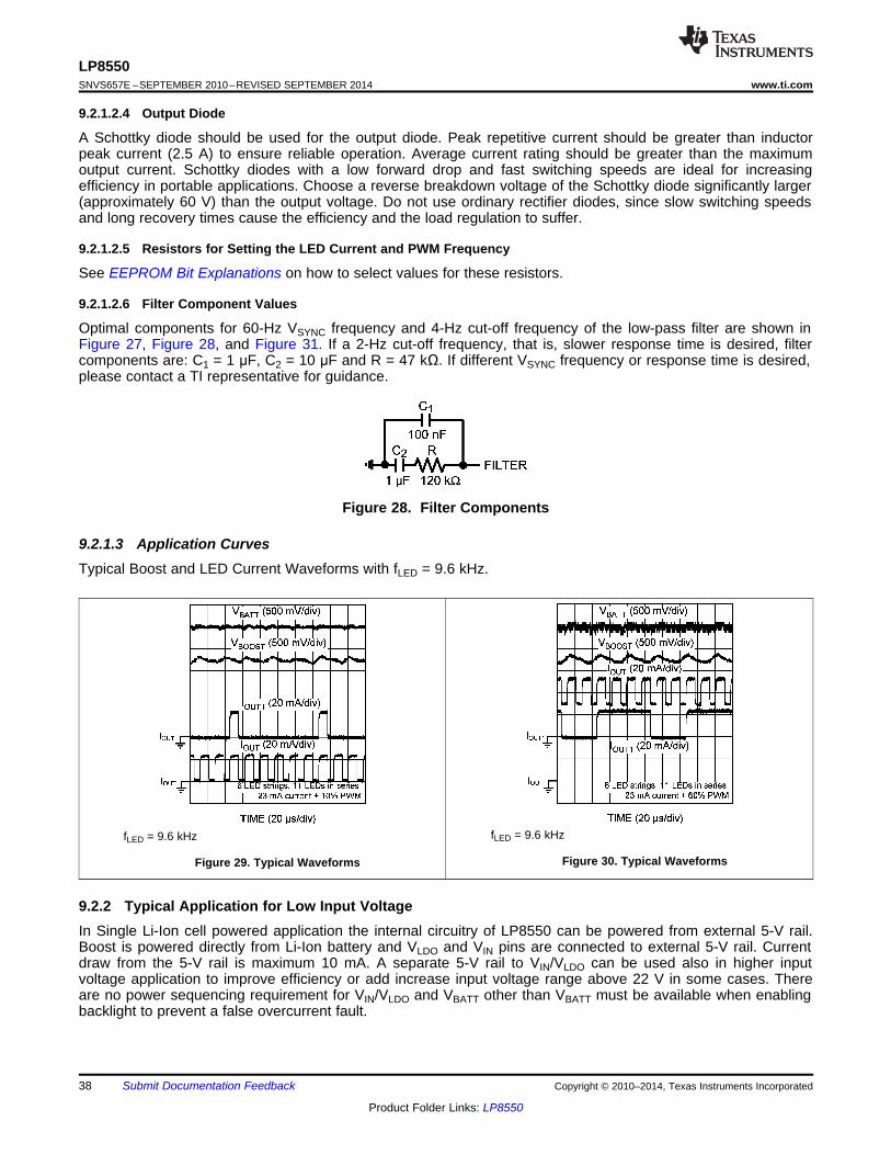
LP8550SNVS657E –SEPTEMBER 2010–REVISED SEPTEMBER 2014 www.ti.com
9.2.1.2.4 Output Diode
A Schottky diode should be used for the output diode. Peak repetitive current should be greater than inductorpeak current (2.5 A) to ensure reliable operation. Average current rating should be greater than the maximumoutput current. Schottky diodes with a low forward drop and fast switching speeds are ideal for increasingefficiency in portable applications. Choose a reverse breakdown voltage of the Schottky diode significantly larger(approximately 60 V) than the output voltage. Do not use ordinary rectifier diodes, since slow switching speedsand long recovery times cause the efficiency and the load regulation to suffer.
9.2.1.2.5 Resistors for Setting the LED Current and PWM Frequency
See EEPROM Bit Explanations on how to select values for these resistors.
9.2.1.2.6 Filter Component Values
Optimal components for 60-Hz VSYNC frequency and 4-Hz cut-off frequency of the low-pass filter are shown inFigure 27, Figure 28, and Figure 31. If a 2-Hz cut-off frequency, that is, slower response time is desired, filtercomponents are: C1 = 1 μF, C2 = 10 μF and R = 47 kΩ. If different VSYNC frequency or response time is desired,please contact a TI representative for guidance.
Figure 28. Filter Components
9.2.1.3 Application CurvesTypical Boost and LED Current Waveforms with fLED = 9.6 kHz.
fLED = 9.6 kHzfLED = 9.6 kHz
Figure 30. Typical WaveformsFigure 29. Typical Waveforms
9.2.2 Typical Application for Low Input VoltageIn Single Li-Ion cell powered application the internal circuitry of LP8550 can be powered from external 5-V rail.Boost is powered directly from Li-Ion battery and VLDO and VIN pins are connected to external 5-V rail. Currentdraw from the 5-V rail is maximum 10 mA. A separate 5-V rail to VIN/VLDO can be used also in higher inputvoltage application to improve efficiency or add increase input voltage range above 22 V in some cases. Thereare no power sequencing requirement for VIN/VLDO and VBATT other than VBATT must be available when enablingbacklight to prevent a false overcurrent fault.
38 Submit Documentation Feedback Copyright © 2010–2014, Texas Instruments Incorporated
Product Folder Links: LP8550
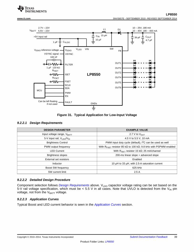
MCU
LP8550
SWFB
VLDO
GNDs
EN
ISET
VDDIO
PWM
SCLKSDA
OUT1
OUT2
OUT3
OUT4
OUT5
OUT6
L1 D12.7V ± 22V
FILTER
+5V input rail
FSET
15 éH
VSYNC
COUTCIN
10 éF 4.7 éFCVLDO1 éF
VDDIO reference voltage
VSYNC signal
120 k5
100 nF
RISET
1 éF
FAULTCan be left floating if not used
39 pF
VIN
RFSET
VBATT 5.5V ± 22V 10 ± 40V, 180 ± 400 mA10 ± 25V, 180 mA
LP8550www.ti.com SNVS657E –SEPTEMBER 2010–REVISED SEPTEMBER 2014
Figure 31. Typical Application for Low-Input Voltage
9.2.2.1 Design Requirements
DESIGN PARAMETER EXAMPLE VALUEInput voltage range, VBATT 2.7 V to VOUT
5-V input rail, VLDO/VIN 4.5 V to 5.5 V, 10 mABrightness Control PWM input duty cycle (default), I2C can be used as well
PWM output frequency With RFSET resistor 85 kΩ to 100 kΩ; 9.8 kHz with PSPWM enabledLED Current With RISET resistor 15 kΩ; 25 mA/channel
Brightness slopes 200-ms linear slope + advanced slopeExternal set resistors Enabled
Inductor 10 µH to 33 µH, with 2.5-A saturation currentBoost SW frequency 625 kHz
SW current limit 2.5 A
9.2.2.2 Detailed Design ProcedureComponent selection follows Design Requirements above. VLDO capacitor voltage rating can be set based on the5-V rail voltage specification, which must be < 5.5 V in all cases. Note that UVLO is detected from the VIN pinvoltage, not from the VBATT voltage.
9.2.2.3 Application CurvesTypical Boost and LED current behavior is seen in the Application Curves section.
Copyright © 2010–2014, Texas Instruments Incorporated Submit Documentation Feedback 39
Product Folder Links: LP8550
LP8550SNVS657E –SEPTEMBER 2010–REVISED SEPTEMBER 2014 www.ti.com
10 Power Supply RecommendationsThe device is designed to operate from an input voltage supply range between 2.7 V and 22 V. This input supplyshould be well-regulated and able to withstand maximum input current and maintain stable voltage withoutvoltage drop even at load transition condition (start-up or rapid brightness change). The resistance of the inputsupply rail should be low enough that the input current transient does not cause drop high enough in the LP8550supply voltage that can cause false UVLO fault triggering.
If a separate 5-V power rail is used to power LP8550 VLDO/VIN pins, this voltage must be stable 4.5 V to 5 V.Excessive noise or ripple in this rail can have adverse effect on device performance, so good grounding andsufficient bypass capacitors must be used. If the input supply is located more than a few inches from the LP8550additional bulk capacitance may be required in addition to the ceramic bypass capacitors. Depending on deviceEEPROM configuration and usage case the boost converter is configured to operate optimally with certain inputvoltage range. Examples are seen in the Detailed Design Procedure section. In uncertain cases, it isrecommended to contact a TI Sales Representative for confirmation of the compatibility of the use case,EEPROM configuration, and input voltage range.
11 Layout
11.1 Layout GuidelinesFigure 33 is a layout recommendation for the LP8550. The figure is used for demonstrating the principle of goodlayout. This layout can be adapted to the actual application layout if/where possible.
It is important that all boost components are close to the chip and the high current traces should be wide enough.By placing the boost component on one side of the chip it is easy to keep the ground plane intact below the highcurrent paths. This way other chip pins can be routed more easily without splitting the ground plane. If the chip isplaced in the center of the boost components, the I2C lines, LED lines, etc. cut the ground plane below the highcurrent paths, and it makes the layout design more difficult.
VIN and VLDO need to be as noise-free as possible. Place the bypass capacitors near the corresponding pins andground them to as noise-free ground as possible.
Here are some main points to help the PCB layout work:1. Current loops need to be minimized:
(a) For low frequency the minimal current loop can be achieved by placing the boost components as close tothe SW and SW_GND pins as possible. Input and output capacitor grounds need to be close to eachother.
(b) Minimal current loops for high frequencies can be achieved by making sure that the ground plane isintact under the current traces. High frequency return currents try to find route with minimum impedance,which is the route with minimum loop area, not necessarily the shortest path. Minimum loop area isformed when return current flows just under the “positive” current route in the ground plane, if the groundplane is intact under the route. Traces from inner pads of the LP8550 need to be routed from below thepart in the second layer so that traces do not split the ground plane under the boost traces orcomponents.
2. GND plane needs to be intact under the high current boost traces to provide shortest possible return pathand smallest possible current loops for high frequencies.
3. Current loops when the boost switch is conducting and not conducting needs to be on the same direction inoptimal case.
4. Inductor placement should be so that the current flows in the same direction as in the current loops. Rotatinginductor 180 degrees changes current direction.
5. Use separate “noisy” and “silent” grounds. Noisy ground is used for boost converter return current and silentground for more sensitive signals, like VIN and VLDO bypass capacitor grounding.
6. Boost output voltage to LEDs need to be taken out “after” the output capacitors, not straight from the diodecathode.
7. Small (such as 39 pF) bypass capacitor should be placed close to the FB pin.8. RISET resistor should be grounded to silent ground, since possible ground ripple will show at the LED current.9. VIN line should be separated from the high current supply path to the boost converter to prevent high
40 Submit Documentation Feedback Copyright © 2010–2014, Texas Instruments Incorporated
Product Folder Links: LP8550

MCU
LP8550
SWFB
VLDO
GND_LED
EN
ISET
VDDIO
PWM
SCLKSDA
OUT1
OUT2
OUT3
OUT4
L1 D1 10V ± 40V5.5V ± 22V
5V
FSET
15 éH
GND
210 mA ± 400 mA
COUT
CIN2 x 10 éF
2 x 10 éF
CVLDO
1 éF
VDDIO reference voltage
FAULTCan be left floating
39 pF
VIN
16 k
91 k
VBATT
GND_S GND_SW
RED line = keep routes short
Sensitive node, quiet ground!
Sensitive node, quiet ground!
Sensitive node, quiet ground!
100 nF
OUT5
OUT6
LP8550www.ti.com SNVS657E –SEPTEMBER 2010–REVISED SEPTEMBER 2014
Layout Guidelines (continued)frequency ripple affecting the chip behavior. Separate 100-nF bypass capacitor is used for VIN line and it isgrounded to noise-free ground.
10. Input and output capacitors need strong grounding (wide traces, vias to GND plane).11. If two output capacitors are used they need symmetrical layout to get both capacitors working ideally.12. Output capacitors DC-bias effect. If the output capacitance is too low, it can cause boost to become
unstable on some loads and this increases EMI. DC bias characteristics need to be obtained from thecomponent manufacturer; it is not taken into account on component tolerance. 50-V 1210-size X5R/X7Rcapacitors are recommended.
11.2 Layout Examples
Figure 32. LP8550 Application Schematic for Layout
Copyright © 2010–2014, Texas Instruments Incorporated Submit Documentation Feedback 41
Product Folder Links: LP8550

LP8550SNVS657E –SEPTEMBER 2010–REVISED SEPTEMBER 2014 www.ti.com
Layout Examples (continued)
Figure 33. LP8550 Layout
42 Submit Documentation Feedback Copyright © 2010–2014, Texas Instruments Incorporated
Product Folder Links: LP8550

LP8550www.ti.com SNVS657E –SEPTEMBER 2010–REVISED SEPTEMBER 2014
12 Device and Documentation Support
12.1 TrademarksAll trademarks are the property of their respective owners.
12.2 Electrostatic Discharge CautionThis integrated circuit can be damaged by ESD. Texas Instruments recommends that all integrated circuits be handled withappropriate precautions. Failure to observe proper handling and installation procedures can cause damage.
ESD damage can range from subtle performance degradation to complete device failure. Precision integrated circuits may be moresusceptible to damage because very small parametric changes could cause the device not to meet its published specifications.
12.3 GlossarySLYZ022 — TI Glossary.
This glossary lists and explains terms, acronyms, and definitions.
13 Mechanical, Packaging, and Orderable InformationThe following pages include mechanical, packaging, and orderable information. This information is the mostcurrent data available for the designated devices. This data is subject to change without notice and revision ofthis document. For browser-based versions of this data sheet, refer to the left-hand navigation.
Copyright © 2010–2014, Texas Instruments Incorporated Submit Documentation Feedback 43
Product Folder Links: LP8550
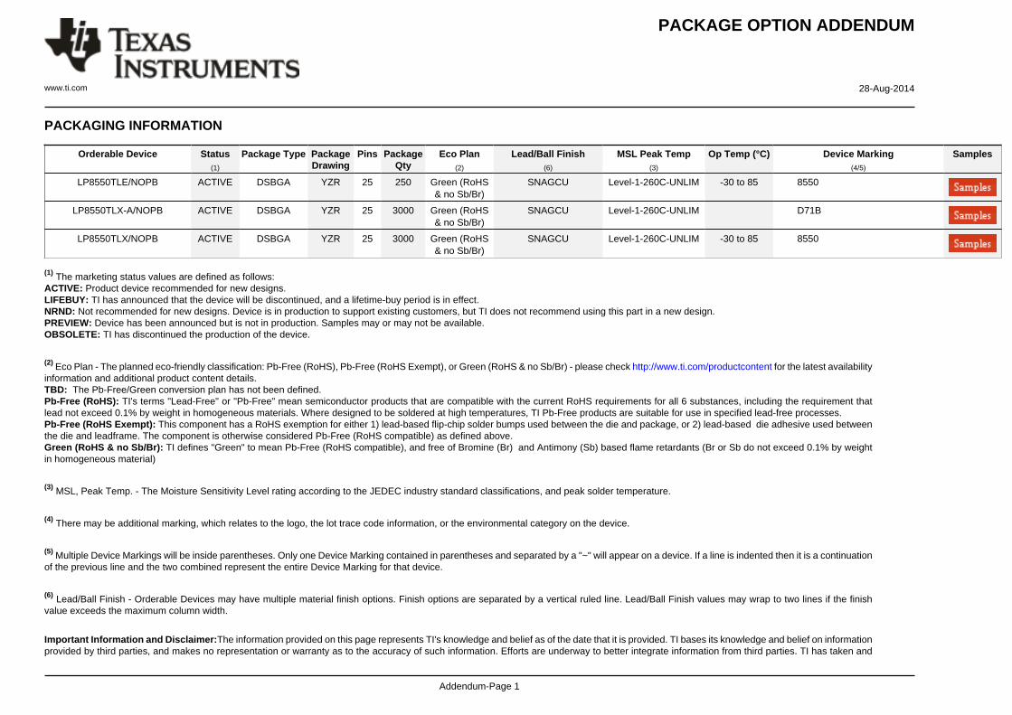
PACKAGE OPTION ADDENDUM
www.ti.com 28-Aug-2014
Addendum-Page 1
PACKAGING INFORMATION
Orderable Device Status(1)
Package Type PackageDrawing
Pins PackageQty
Eco Plan(2)
Lead/Ball Finish(6)
MSL Peak Temp(3)
Op Temp (°C) Device Marking(4/5)
Samples
LP8550TLE/NOPB ACTIVE DSBGA YZR 25 250 Green (RoHS& no Sb/Br)
SNAGCU Level-1-260C-UNLIM -30 to 85 8550
LP8550TLX-A/NOPB ACTIVE DSBGA YZR 25 3000 Green (RoHS& no Sb/Br)
SNAGCU Level-1-260C-UNLIM D71B
LP8550TLX/NOPB ACTIVE DSBGA YZR 25 3000 Green (RoHS& no Sb/Br)
SNAGCU Level-1-260C-UNLIM -30 to 85 8550
(1) The marketing status values are defined as follows:ACTIVE: Product device recommended for new designs.LIFEBUY: TI has announced that the device will be discontinued, and a lifetime-buy period is in effect.NRND: Not recommended for new designs. Device is in production to support existing customers, but TI does not recommend using this part in a new design.PREVIEW: Device has been announced but is not in production. Samples may or may not be available.OBSOLETE: TI has discontinued the production of the device.
(2) Eco Plan - The planned eco-friendly classification: Pb-Free (RoHS), Pb-Free (RoHS Exempt), or Green (RoHS & no Sb/Br) - please check http://www.ti.com/productcontent for the latest availabilityinformation and additional product content details.TBD: The Pb-Free/Green conversion plan has not been defined.Pb-Free (RoHS): TI's terms "Lead-Free" or "Pb-Free" mean semiconductor products that are compatible with the current RoHS requirements for all 6 substances, including the requirement thatlead not exceed 0.1% by weight in homogeneous materials. Where designed to be soldered at high temperatures, TI Pb-Free products are suitable for use in specified lead-free processes.Pb-Free (RoHS Exempt): This component has a RoHS exemption for either 1) lead-based flip-chip solder bumps used between the die and package, or 2) lead-based die adhesive used betweenthe die and leadframe. The component is otherwise considered Pb-Free (RoHS compatible) as defined above.Green (RoHS & no Sb/Br): TI defines "Green" to mean Pb-Free (RoHS compatible), and free of Bromine (Br) and Antimony (Sb) based flame retardants (Br or Sb do not exceed 0.1% by weightin homogeneous material)
(3) MSL, Peak Temp. - The Moisture Sensitivity Level rating according to the JEDEC industry standard classifications, and peak solder temperature.
(4) There may be additional marking, which relates to the logo, the lot trace code information, or the environmental category on the device.
(5) Multiple Device Markings will be inside parentheses. Only one Device Marking contained in parentheses and separated by a "~" will appear on a device. If a line is indented then it is a continuationof the previous line and the two combined represent the entire Device Marking for that device.
(6) Lead/Ball Finish - Orderable Devices may have multiple material finish options. Finish options are separated by a vertical ruled line. Lead/Ball Finish values may wrap to two lines if the finishvalue exceeds the maximum column width.
Important Information and Disclaimer:The information provided on this page represents TI's knowledge and belief as of the date that it is provided. TI bases its knowledge and belief on informationprovided by third parties, and makes no representation or warranty as to the accuracy of such information. Efforts are underway to better integrate information from third parties. TI has taken and
PACKAGE OPTION ADDENDUM
www.ti.com 28-Aug-2014
Addendum-Page 2
continues to take reasonable steps to provide representative and accurate information but may not have conducted destructive testing or chemical analysis on incoming materials and chemicals.TI and TI suppliers consider certain information to be proprietary, and thus CAS numbers and other limited information may not be available for release.
In no event shall TI's liability arising out of such information exceed the total purchase price of the TI part(s) at issue in this document sold by TI to Customer on an annual basis.
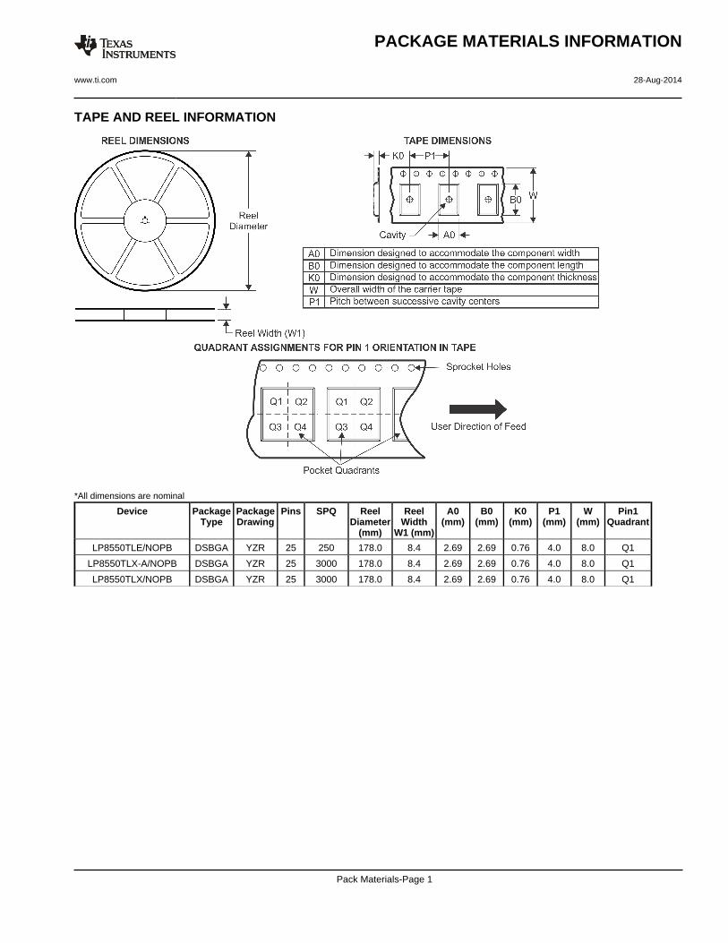
TAPE AND REEL INFORMATION
*All dimensions are nominal
Device PackageType
PackageDrawing
Pins SPQ ReelDiameter
(mm)
ReelWidth
W1 (mm)
A0(mm)
B0(mm)
K0(mm)
P1(mm)
W(mm)
Pin1Quadrant
LP8550TLE/NOPB DSBGA YZR 25 250 178.0 8.4 2.69 2.69 0.76 4.0 8.0 Q1
LP8550TLX-A/NOPB DSBGA YZR 25 3000 178.0 8.4 2.69 2.69 0.76 4.0 8.0 Q1
LP8550TLX/NOPB DSBGA YZR 25 3000 178.0 8.4 2.69 2.69 0.76 4.0 8.0 Q1
PACKAGE MATERIALS INFORMATION
www.ti.com 28-Aug-2014
Pack Materials-Page 1
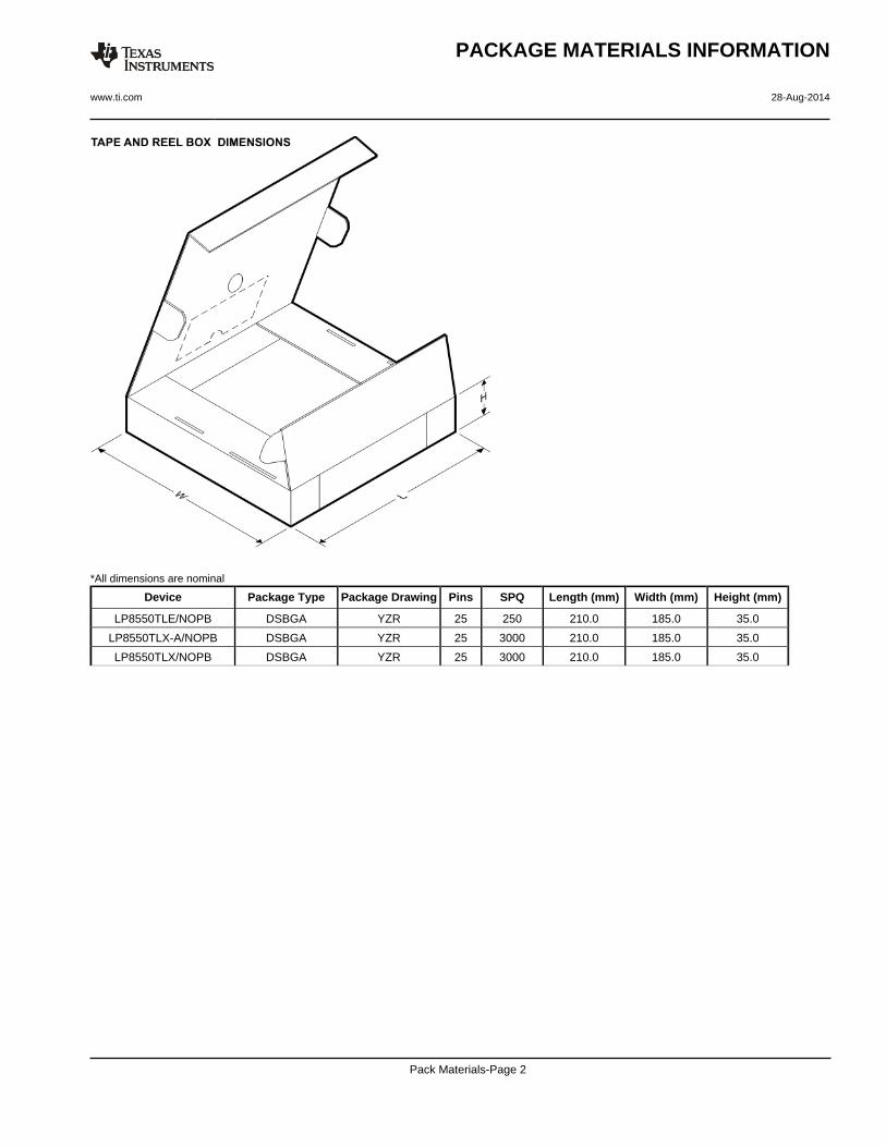
*All dimensions are nominal
Device Package Type Package Drawing Pins SPQ Length (mm) Width (mm) Height (mm)
LP8550TLE/NOPB DSBGA YZR 25 250 210.0 185.0 35.0
LP8550TLX-A/NOPB DSBGA YZR 25 3000 210.0 185.0 35.0
LP8550TLX/NOPB DSBGA YZR 25 3000 210.0 185.0 35.0
PACKAGE MATERIALS INFORMATION
www.ti.com 28-Aug-2014
Pack Materials-Page 2
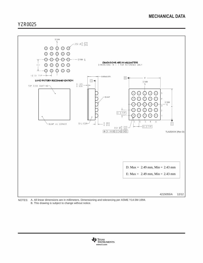
MECHANICAL DATA
YZR0025xxx
www.ti.com
TLA25XXX (Rev D)
0.600±0.075D
E
A. All linear dimensions are in millimeters. Dimensioning and tolerancing per ASME Y14.5M-1994.B. This drawing is subject to change without notice.
NOTES:
4215055/A 12/12
D: Max =
E: Max =
2.49 mm, Min =
2.49 mm, Min =
2.43 mm
2.43 mm
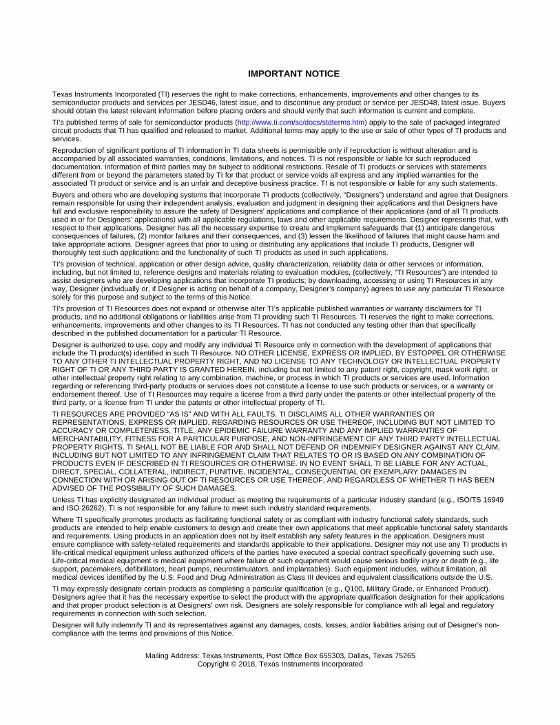
IMPORTANT NOTICE
Texas Instruments Incorporated (TI) reserves the right to make corrections, enhancements, improvements and other changes to itssemiconductor products and services per JESD46, latest issue, and to discontinue any product or service per JESD48, latest issue. Buyersshould obtain the latest relevant information before placing orders and should verify that such information is current and complete.TI’s published terms of sale for semiconductor products (http://www.ti.com/sc/docs/stdterms.htm) apply to the sale of packaged integratedcircuit products that TI has qualified and released to market. Additional terms may apply to the use or sale of other types of TI products andservices.Reproduction of significant portions of TI information in TI data sheets is permissible only if reproduction is without alteration and isaccompanied by all associated warranties, conditions, limitations, and notices. TI is not responsible or liable for such reproduceddocumentation. Information of third parties may be subject to additional restrictions. Resale of TI products or services with statementsdifferent from or beyond the parameters stated by TI for that product or service voids all express and any implied warranties for theassociated TI product or service and is an unfair and deceptive business practice. TI is not responsible or liable for any such statements.Buyers and others who are developing systems that incorporate TI products (collectively, “Designers”) understand and agree that Designersremain responsible for using their independent analysis, evaluation and judgment in designing their applications and that Designers havefull and exclusive responsibility to assure the safety of Designers' applications and compliance of their applications (and of all TI productsused in or for Designers’ applications) with all applicable regulations, laws and other applicable requirements. Designer represents that, withrespect to their applications, Designer has all the necessary expertise to create and implement safeguards that (1) anticipate dangerousconsequences of failures, (2) monitor failures and their consequences, and (3) lessen the likelihood of failures that might cause harm andtake appropriate actions. Designer agrees that prior to using or distributing any applications that include TI products, Designer willthoroughly test such applications and the functionality of such TI products as used in such applications.TI’s provision of technical, application or other design advice, quality characterization, reliability data or other services or information,including, but not limited to, reference designs and materials relating to evaluation modules, (collectively, “TI Resources”) are intended toassist designers who are developing applications that incorporate TI products; by downloading, accessing or using TI Resources in anyway, Designer (individually or, if Designer is acting on behalf of a company, Designer’s company) agrees to use any particular TI Resourcesolely for this purpose and subject to the terms of this Notice.TI’s provision of TI Resources does not expand or otherwise alter TI’s applicable published warranties or warranty disclaimers for TIproducts, and no additional obligations or liabilities arise from TI providing such TI Resources. TI reserves the right to make corrections,enhancements, improvements and other changes to its TI Resources. TI has not conducted any testing other than that specificallydescribed in the published documentation for a particular TI Resource.Designer is authorized to use, copy and modify any individual TI Resource only in connection with the development of applications thatinclude the TI product(s) identified in such TI Resource. NO OTHER LICENSE, EXPRESS OR IMPLIED, BY ESTOPPEL OR OTHERWISETO ANY OTHER TI INTELLECTUAL PROPERTY RIGHT, AND NO LICENSE TO ANY TECHNOLOGY OR INTELLECTUAL PROPERTYRIGHT OF TI OR ANY THIRD PARTY IS GRANTED HEREIN, including but not limited to any patent right, copyright, mask work right, orother intellectual property right relating to any combination, machine, or process in which TI products or services are used. Informationregarding or referencing third-party products or services does not constitute a license to use such products or services, or a warranty orendorsement thereof. Use of TI Resources may require a license from a third party under the patents or other intellectual property of thethird party, or a license from TI under the patents or other intellectual property of TI.TI RESOURCES ARE PROVIDED “AS IS” AND WITH ALL FAULTS. TI DISCLAIMS ALL OTHER WARRANTIES ORREPRESENTATIONS, EXPRESS OR IMPLIED, REGARDING RESOURCES OR USE THEREOF, INCLUDING BUT NOT LIMITED TOACCURACY OR COMPLETENESS, TITLE, ANY EPIDEMIC FAILURE WARRANTY AND ANY IMPLIED WARRANTIES OFMERCHANTABILITY, FITNESS FOR A PARTICULAR PURPOSE, AND NON-INFRINGEMENT OF ANY THIRD PARTY INTELLECTUALPROPERTY RIGHTS. TI SHALL NOT BE LIABLE FOR AND SHALL NOT DEFEND OR INDEMNIFY DESIGNER AGAINST ANY CLAIM,INCLUDING BUT NOT LIMITED TO ANY INFRINGEMENT CLAIM THAT RELATES TO OR IS BASED ON ANY COMBINATION OFPRODUCTS EVEN IF DESCRIBED IN TI RESOURCES OR OTHERWISE. IN NO EVENT SHALL TI BE LIABLE FOR ANY ACTUAL,DIRECT, SPECIAL, COLLATERAL, INDIRECT, PUNITIVE, INCIDENTAL, CONSEQUENTIAL OR EXEMPLARY DAMAGES INCONNECTION WITH OR ARISING OUT OF TI RESOURCES OR USE THEREOF, AND REGARDLESS OF WHETHER TI HAS BEENADVISED OF THE POSSIBILITY OF SUCH DAMAGES.Unless TI has explicitly designated an individual product as meeting the requirements of a particular industry standard (e.g., ISO/TS 16949and ISO 26262), TI is not responsible for any failure to meet such industry standard requirements.Where TI specifically promotes products as facilitating functional safety or as compliant with industry functional safety standards, suchproducts are intended to help enable customers to design and create their own applications that meet applicable functional safety standardsand requirements. Using products in an application does not by itself establish any safety features in the application. Designers mustensure compliance with safety-related requirements and standards applicable to their applications. Designer may not use any TI products inlife-critical medical equipment unless authorized officers of the parties have executed a special contract specifically governing such use.Life-critical medical equipment is medical equipment where failure of such equipment would cause serious bodily injury or death (e.g., lifesupport, pacemakers, defibrillators, heart pumps, neurostimulators, and implantables). Such equipment includes, without limitation, allmedical devices identified by the U.S. Food and Drug Administration as Class III devices and equivalent classifications outside the U.S.TI may expressly designate certain products as completing a particular qualification (e.g., Q100, Military Grade, or Enhanced Product).Designers agree that it has the necessary expertise to select the product with the appropriate qualification designation for their applicationsand that proper product selection is at Designers’ own risk. Designers are solely responsible for compliance with all legal and regulatoryrequirements in connection with such selection.Designer will fully indemnify TI and its representatives against any damages, costs, losses, and/or liabilities arising out of Designer’s non-compliance with the terms and provisions of this Notice.
Mailing Address: Texas Instruments, Post Office Box 655303, Dallas, Texas 75265Copyright © 2018, Texas Instruments Incorporated