Embed Size (px)
Citation preview
1. General description
The LPC1102/1104 are an ARM Cortex-M0 based, low-cost 32-bit MCU, designed for 8/16-bit microcontroller applications, offering performance, low power, simple instruction set and memory addressing together with reduced code size compared to existing 8/16-bit architectures.
The LPC1102/1104 operate at CPU frequencies of up to 50 MHz.
The peripheral complement of the LPC1102/1104 includes 32 kB of flash memory, 8 kB of data memory, one RS-485/EIA-485 UART, one SPI interface with SSP features, four general purpose counter/timers, a 10-bit ADC, and 11 general purpose I/O pins.
Remark: The LPC1104 has a revised pinout and contains several features not found in the LPC1102:
• Two extra GPIO pins (PIO0_1 and PIO0_6).
• Extra match output (CT32B0_MAT2).
• CLKOUT feature.
• Easier re-entry to ISP via PIO0_1.
• SSP0_CLK available on two pins (A1 and A2) to support debugging of SSP communication.
• Better positioning of the XTALIN pin for easier PCB layout.
2. Features and benefits
System:
ARM Cortex-M0 processor, running at frequencies of up to 50 MHz.
ARM Cortex-M0 built-in Nested Vectored Interrupt Controller (NVIC).
Serial Wire Debug.
System tick timer.
Memory:
32 kB on-chip flash programming memory.
8 kB SRAM.
In-Application Programming (IAP) and In-System Programming (ISP) support via on-chip bootloader software.
Digital peripherals:
11 General Purpose I/O (GPIO) pins with configurable pull-up/pull-down resistors and programmable open-drain mode.
LPC1102/110432-bit ARM Cortex-M0 microcontroller; 32 kB flash and 8 kB SRAMRev. 7 — 26 September 2013 Product data sheet
NXP Semiconductors LPC1102/1104 32-bit ARM Cortex-M0 microcontroller
GPIO pins can be used as edge and level sensitive interrupt sources.
Four general purpose counter/timers with a total of one capture input and 10 match outputs.
Programmable windowed WatchDog Timer (WDT).
Analog peripherals:
10-bit ADC with input multiplexing among five pins.
Serial interfaces:
UART with fractional baud rate generation, internal FIFO, and RS-485 support.
One SPI controller with SSP features and with FIFO and multi-protocol capabilities (see Section 7.16).
Clock generation:
12 MHz internal RC oscillator trimmed to 1 % accuracy that can optionally be used as a system clock.
Programmable watchdog oscillator with a frequency range of 9.4 kHz to 2.3 MHz.
PLL allows CPU operation up to the maximum CPU rate without the need for a high-frequency crystal. May be run from an external clock or the internal RC oscillator.
Clock output function with divider that can reflect the system oscillator clock, IRC clock, CPU clock, and the Watchdog clock (LPC1104 only).
Power control:
Integrated PMU (Power Management Unit) to minimize power consumption during Sleep and Deep-sleep modes.
Power profiles residing in boot ROM allowing to optimize performance and minimize power consumption for any given application through one simple function call.
Two reduced power modes: Sleep and Deep-sleep modes.
Processor wake-up from Deep-sleep mode via a dedicated start logic using up to six of the functional pins.
Power-On Reset (POR).
Brownout detect with up to four separate thresholds for interrupt and forced reset.
Unique device serial number for identification.
Single 3.3 V power supply (1.8 V to 3.6 V).
Available as WLCSP16 package.
3. Applications
Mobile devices 8-/16-bit applications
Consumer peripherals Portable devices
Lighting
LPC1102_1104 All information provided in this document is subject to legal disclaimers. © NXP B.V. 2013. All rights reserved.
Product data sheet Rev. 7 — 26 September 2013 2 of 43
NXP Semiconductors LPC1102/1104 32-bit ARM Cortex-M0 microcontroller
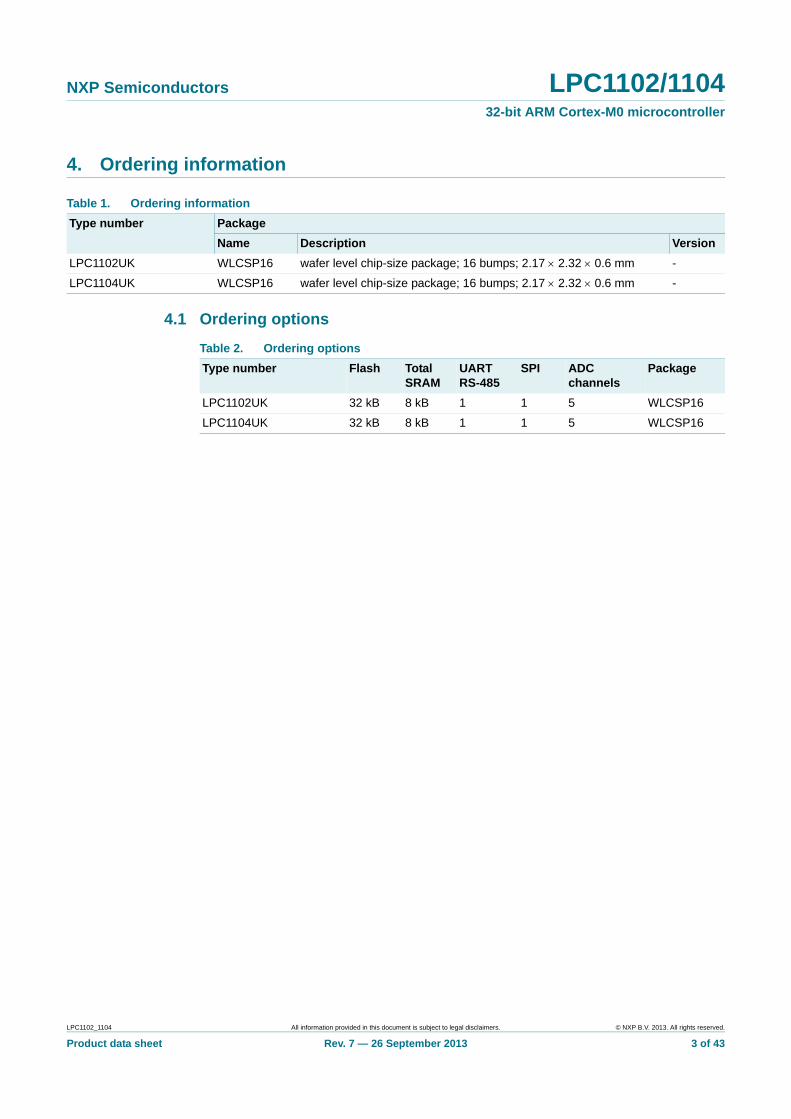
4. Ordering information
4.1 Ordering options
Table 1. Ordering information
Type number Package
Name Description Version
LPC1102UK WLCSP16 wafer level chip-size package; 16 bumps; 2.17 2.32 0.6 mm -
LPC1104UK WLCSP16 wafer level chip-size package; 16 bumps; 2.17 2.32 0.6 mm -
Table 2. Ordering options
Type number Flash Total SRAM
UART RS-485
SPI ADC channels
Package
LPC1102UK 32 kB 8 kB 1 1 5 WLCSP16
LPC1104UK 32 kB 8 kB 1 1 5 WLCSP16
LPC1102_1104 All information provided in this document is subject to legal disclaimers. © NXP B.V. 2013. All rights reserved.
Product data sheet Rev. 7 — 26 September 2013 3 of 43
NXP Semiconductors LPC1102/1104 32-bit ARM Cortex-M0 microcontroller
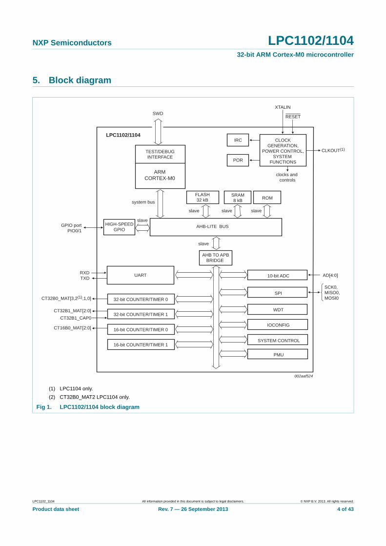
5. Block diagram
(1) LPC1104 only.
(2) CT32B0_MAT2 LPC1104 only.
Fig 1. LPC1102/1104 block diagram
SRAM8 kB
ARMCORTEX-M0
TEST/DEBUGINTERFACE
FLASH32 kB
HIGH-SPEEDGPIO
AHB TO APBBRIDGE
CLOCKGENERATION,
POWER CONTROL,SYSTEM
FUNCTIONS
XTALIN
RESET
clocks and controls
SWD
LPC1102/1104
002aaf524
slave
slave
slave slave
ROM
slave
AHB-LITE BUSGPIO portPIO0/1
IRC
POR
SPI
10-bit ADCUART
32-bit COUNTER/TIMER 0
WDT
IOCONFIG
CT32B0_MAT[3,2(1),1,0]
AD[4:0]RXDTXD
SYSTEM CONTROL
PMU
32-bit COUNTER/TIMER 1CT32B1_MAT[2:0]
CT32B1_CAP0
16-bit COUNTER/TIMER 1
16-bit COUNTER/TIMER 0CT16B0_MAT[2:0]
SCK0, MISO0,MOSI0
system bus
CLKOUT(1)
LPC1102_1104 All information provided in this document is subject to legal disclaimers. © NXP B.V. 2013. All rights reserved.
Product data sheet Rev. 7 — 26 September 2013 4 of 43
NXP Semiconductors LPC1102/1104 32-bit ARM Cortex-M0 microcontroller
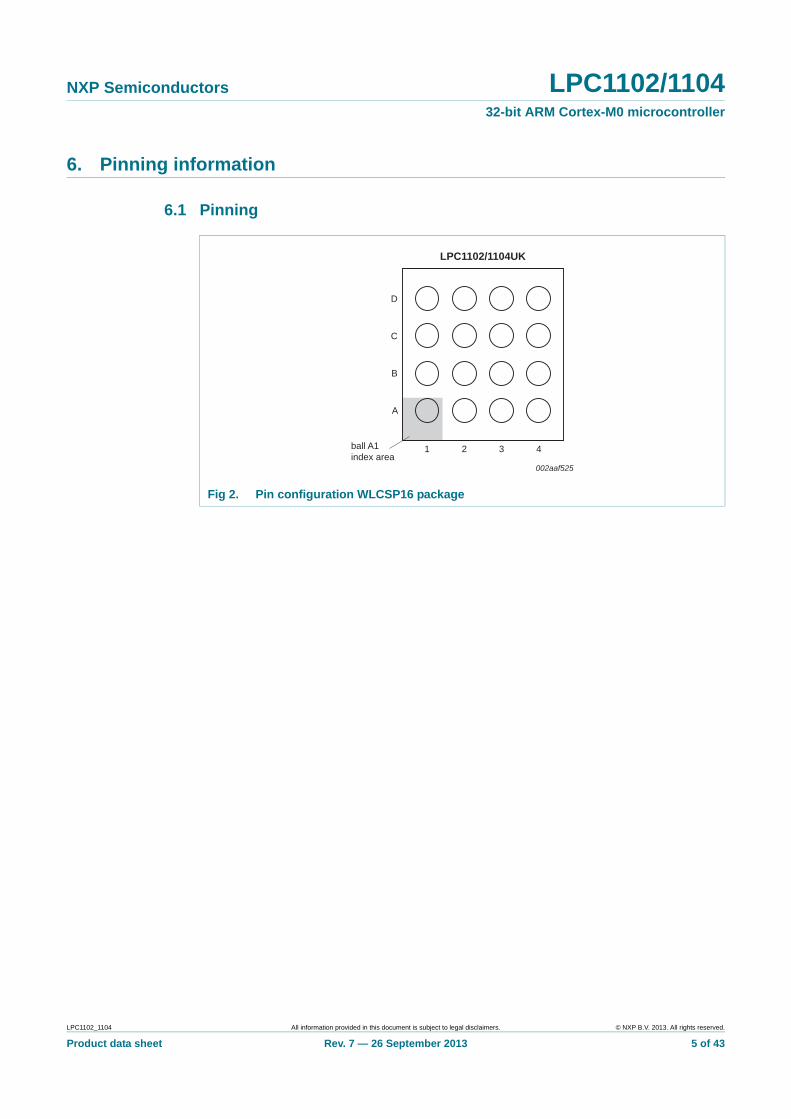
6. Pinning information
6.1 Pinning
Fig 2. Pin configuration WLCSP16 package
002aaf525
ball A1index area
1 2 3 4
A
B
C
D
LPC1102/1104UK
LPC1102_1104 All information provided in this document is subject to legal disclaimers. © NXP B.V. 2013. All rights reserved.
Product data sheet Rev. 7 — 26 September 2013 5 of 43
NXP Semiconductors LPC1102/1104 32-bit ARM Cortex-M0 microcontroller
6.2 Pin description
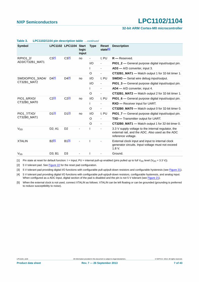
Table 3. LPC1102/1104 pin description table
Symbol LPC1102 LPC1104 Start logic input
Type Reset state[1]
Description
RESET/PIO0_0 C1[2] B2[2] yes I I; PU RESET — External reset input with 20 ns glitch filter. A LOW -going pulse as short as 50 ns on this pin resets the device, causing I/O ports and peripherals to take on their default states, and processor execution to begin at address 0.
I/O - PIO0_0 — General purpose digital input/output pin.
PIO0_1/CLKOUT/
CT32B0_MAT2
- C1[3] yes I/O I; PU PIO0_1 — General purpose digital input/output pin. A LOW level on this pin during reset starts the ISP command handler.
O - CLKOUT — Clockout pin.
O - CT32B0_MAT2 — Match output 2 for 32-bit timer 0.
PIO0_6/SCK0 - A1[3] yes I/O I;PU PIO0_6 — General purpose digital input/output pin.
I/O - SCK0 — Serial clock for SPI0.
PIO0_8/MISO/CT16B0_MAT0
A2[3] A3[3] yes I/O I; PU PIO0_8 — General purpose digital input/output pin.
I/O - MISO0 — Master In Slave Out for SPI.
O - CT16B0_MAT0 — Match output 0 for 16-bit timer 0.
PIO0_9/MOSI/CT16B0_MAT1
A3[3] A4[3] yes I/O I; PU PIO0_9 — General purpose digital input/output pin.
I/O - MOSI0 — Master Out Slave In for SPI.
O - CT16B0_MAT1 — Match output 1 for 16-bit timer 0.
SWCLK/PIO0_10/SCK0/CT16B0_MAT2
A4[3] A2[3] yes I I; PU SWCLK — Serial wire clock.
I/O - PIO0_10 — General purpose digital input/output pin.
I/O - SCK0 — Serial clock for SPI0.
O - CT16B0_MAT2 — Match output 2 for 16-bit timer 0.
R/PIO0_11/AD0/CT32B0_MAT3
B4[4] B4[4] yes - I; PU R — Reserved.
I/O - PIO0_11 — General purpose digital input/output pin.
I - AD0 — A/D converter, input 0.
I - CT32B0_MAT3 — Match output 3 for 32-bit timer 0.
R/PIO1_0/AD1/CT32B1_CAP0
B3[4] B3[4] yes - I; PU R — Reserved.
I/O - PIO1_0 — General purpose digital input/output pin.
I - AD1 — A/D converter, input 1.
I - CT32B1_CAP0 — Capture input 0 for 32-bit timer 1.
R/PIO1_1/AD2/CT32B1_MAT0
C4[4] C4[4] no - I; PU R — Reserved.
I/O - PIO1_1 — General purpose digital input/output pin.
I - AD2 — A/D converter, input 2.
O - CT32B1_MAT0 — Match output 0 for 32-bit timer 1.
LPC1102_1104 All information provided in this document is subject to legal disclaimers. © NXP B.V. 2013. All rights reserved.
Product data sheet Rev. 7 — 26 September 2013 6 of 43
NXP Semiconductors LPC1102/1104 32-bit ARM Cortex-M0 microcontroller
[1] Pin state at reset for default function: I = Input; PU = internal pull-up enabled (pins pulled up to full VDD level (VDD = 3.3 V)).
[2] 5 V tolerant pad. See Figure 22 for the reset pad configuration.
[3] 5 V tolerant pad providing digital I/O functions with configurable pull-up/pull-down resistors and configurable hysteresis (see Figure 21).
[4] 5 V tolerant pad providing digital I/O functions with configurable pull-up/pull-down resistors, configurable hysteresis, and analog input. When configured as a ADC input, digital section of the pad is disabled and the pin is not 5 V tolerant (see Figure 21).
[5] When the external clock is not used, connect XTALIN as follows: XTALIN can be left floating or can be grounded (grounding is preferred to reduce susceptibility to noise).
R/PIO1_2/AD3/CT32B1_MAT1
C3[4] C3[4] no - I; PU R — Reserved.
I/O - PIO1_2 — General purpose digital input/output pin.
I - AD3 — A/D converter, input 3.
O - CT32B1_MAT1 — Match output 1 for 32-bit timer 1.
SWDIO/PIO1_3/AD4/CT32B1_MAT2
D4[4] D4[4] no I/O I; PU SWDIO — Serial wire debug input/output.
I/O - PIO1_3 — General purpose digital input/output pin.
I - AD4 — A/D converter, input 4.
O - CT32B1_MAT2 — Match output 2 for 32-bit timer 1.
PIO1_6/RXD/CT32B0_MAT0
C2[3] C2[3] no I/O I; PU PIO1_6 — General purpose digital input/output pin.
I - RXD — Receiver input for UART.
O - CT32B0_MAT0 — Match output 0 for 32-bit timer 0.
PIO1_7/TXD/CT32B0_MAT1
D1[3] D1[3] no I/O I; PU PIO1_7 — General purpose digital input/output pin.
O - TXD — Transmitter output for UART.
O - CT32B0_MAT1 — Match output 1 for 32-bit timer 0.
VDD D2; A1 D2 - I - 3.3 V supply voltage to the internal regulator, the external rail, and the ADC. Also used as the ADC reference voltage.
XTALIN B2[5] B1[5] - I - External clock input and input to internal clock generator circuits. Input voltage must not exceed 1.8 V.
VSS D3; B1 D3 - I - Ground.
Table 3. LPC1102/1104 pin description table …continued
Symbol LPC1102 LPC1104 Start logic input
Type Reset state[1]
Description
LPC1102_1104 All information provided in this document is subject to legal disclaimers. © NXP B.V. 2013. All rights reserved.
Product data sheet Rev. 7 — 26 September 2013 7 of 43
NXP Semiconductors LPC1102/1104 32-bit ARM Cortex-M0 microcontroller
7. Functional description
7.1 ARM Cortex-M0 processor
The ARM Cortex-M0 is a general purpose, 32-bit microprocessor, which offers high performance and very low power consumption.
7.2 On-chip flash program memory
The LPC1102/1104 contain 32 kB of on-chip flash memory.
Remark: The LPC1102 supports In-Application Programming (IAP) and In-System Programming (ISP). For ISP, since there is no dedicated ISP entry pin, user code is required to invoke ISP functionality. Unprogrammed parts will automatically boot into ISP mode.
7.3 On-chip SRAM
The LPC1102/1104 contain 8 kB on-chip static RAM memory.
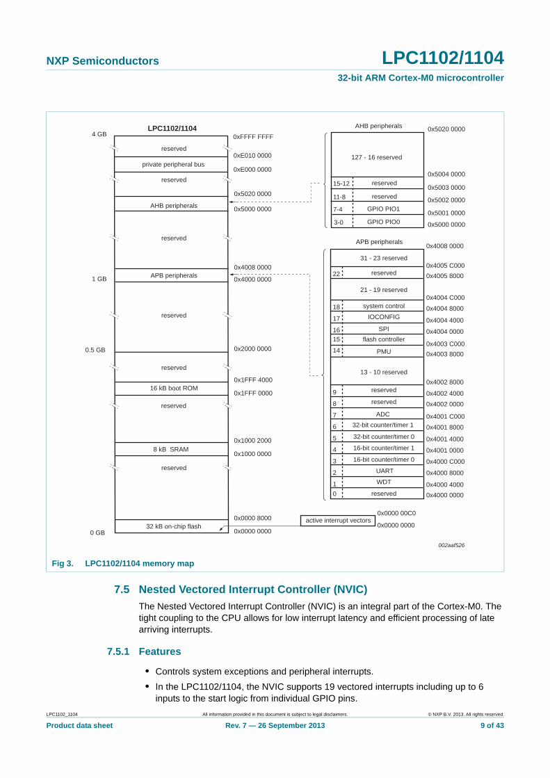
7.4 Memory map
The LPC1102/1104 incorporate several distinct memory regions, shown in the following figures. Figure 3 shows the overall map of the entire address space from the user program viewpoint following reset. The interrupt vector area supports address remapping.
The AHB peripheral area is 2 MB in size, and is divided to allow for up to 128 peripherals. The APB peripheral area is 512 kB in size and is divided to allow for up to 32 peripherals. Each peripheral of either type is allocated 16 kB of space. This allows simplifying the address decoding for each peripheral.
LPC1102_1104 All information provided in this document is subject to legal disclaimers. © NXP B.V. 2013. All rights reserved.
Product data sheet Rev. 7 — 26 September 2013 8 of 43
NXP Semiconductors LPC1102/1104 32-bit ARM Cortex-M0 microcontroller
7.5 Nested Vectored Interrupt Controller (NVIC)
The Nested Vectored Interrupt Controller (NVIC) is an integral part of the Cortex-M0. The tight coupling to the CPU allows for low interrupt latency and efficient processing of late arriving interrupts.
7.5.1 Features
• Controls system exceptions and peripheral interrupts.
• In the LPC1102/1104, the NVIC supports 19 vectored interrupts including up to 6 inputs to the start logic from individual GPIO pins.
Fig 3. LPC1102/1104 memory map
0x5000 0000
0x5001 0000
0x5002 0000
0x5020 0000AHB peripherals
127 - 16 reserved
GPIO PIO1 7-4
0x5003 0000
0x5004 0000
reserved
reserved
11-8
15-12
GPIO PIO0 3-0
APB peripherals
0x4000 4000
0x4000 8000
0x4000 C000
0x4001 0000
0x4001 8000
0x4002 0000
0x4002 8000
0x4003 80000x4003 C000
0x4004 0000
0x4004 4000
0x4004 8000
0x4004 C000
0x4005 80000x4005 C000
0x4008 0000
0x4002 4000
0x4001 C000
0x4001 4000
0x4000 0000
WDT
32-bit counter/timer 0
32-bit counter/timer 1 ADC
UART
PMU
reserved
13 - 10 reserved
reserved
reserved
21 - 19 reserved
31 - 23 reserved
01
2
3
4
5
6
7
8
9
1615
14
17
18
reserved
reserved
reserved
0x0000 00000 GB
0.5 GB
4 GB
1 GB
0x1000 2000
0x1FFF 0000
0x1FFF 4000
0x2000 0000
0x4000 0000
0x4008 0000
0x5000 0000
0x5020 0000
0xFFFF FFFF
reserved
reserved
reserved
APB peripherals
AHB peripherals
8 kB SRAM 0x1000 0000
LPC1102/1104
0x0000 800032 kB on-chip flash
16 kB boot ROM
0x0000 0000
0x0000 00C0active interrupt vectors
002aaf526
reserved
SPI
16-bit counter/timer 1
16-bit counter/timer 0
IOCONFIG
system control
22 reserved
flash controller
0xE000 0000
0xE010 0000private peripheral bus
LPC1102_1104 All information provided in this document is subject to legal disclaimers. © NXP B.V. 2013. All rights reserved.
Product data sheet Rev. 7 — 26 September 2013 9 of 43
NXP Semiconductors LPC1102/1104 32-bit ARM Cortex-M0 microcontroller
• Four programmable interrupt priority levels, with hardware priority level masking.
• Software interrupt generation.
7.5.2 Interrupt sources
Each peripheral device has one interrupt line connected to the NVIC but may have several interrupt flags. Individual interrupt flags may also represent more than one interrupt source.
Any GPIO pin (total of up to 11 pins) regardless of the selected function, can be programmed to generate an interrupt on a level, or rising edge or falling edge, or both.
7.6 IOCONFIG block
The IOCONFIG block allows selected pins of the microcontroller to have more than one function. Configuration registers control the multiplexers to allow connection between the pin and the on-chip peripherals.
Peripherals should be connected to the appropriate pins prior to being activated and prior to any related interrupt(s) being enabled. Activity of any enabled peripheral function that is not mapped to a related pin should be considered undefined.
7.7 Fast general purpose parallel I/O
Device pins that are not connected to a specific peripheral function are controlled by the GPIO registers. Pins may be dynamically configured as inputs or outputs. Multiple outputs can be set or cleared in one write operation.
The LPC1102/1104 use accelerated GPIO functions:
• GPIO registers are a dedicated AHB peripheral so that the fastest possible I/O timing can be achieved.
• Entire port value can be written in one instruction.
Additionally, any GPIO pin (total of 11 pins) providing a digital function can be programmed to generate an interrupt on a level, a rising or falling edge, or both.
7.7.1 Features
• Bit level port registers allow a single instruction to set or clear any number of bits in one write operation.
• Direction control of individual bits.
• All I/O default to inputs with pull-ups enabled after reset.
• Pull-up/pull-down resistor configuration can be programmed through the IOCONFIG block for each GPIO pin.
• All GPIO pins are pulled up to 3.3 V (VDD = 3.3 V) if their pull-up resistor is enabled in the IOCONFIG block.
• Programmable open-drain mode.
7.8 UART
The LPC1102/1104 contain one UART.
LPC1102_1104 All information provided in this document is subject to legal disclaimers. © NXP B.V. 2013. All rights reserved.
Product data sheet Rev. 7 — 26 September 2013 10 of 43
NXP Semiconductors LPC1102/1104 32-bit ARM Cortex-M0 microcontroller
Support for RS-485/9-bit mode allows both software address detection and automatic address detection using 9-bit mode.
The UART includes a fractional baud rate generator. Standard baud rates such as 115200 Bd can be achieved with any crystal frequency above 2 MHz.
7.8.1 Features
• Maximum UART data bit rate of 3.125 Mbit/s.
• 16 Byte Receive and Transmit FIFOs.
• Register locations conform to 16C550 industry standard.
• Receiver FIFO trigger points at 1 B, 4 B, 8 B, and 14 B.
• Built-in fractional baud rate generator covering wide range of baud rates without a need for external crystals of particular values.
• FIFO control mechanism that enables software flow control implementation.
• Support for RS-485/9-bit mode.
7.9 SPI serial I/O controller
The LPC1102/1104 contain one SPI controller and fully supports SSP features.
The SPI controller is capable of operation on a SSP, 4-wire SSI, or Microwire bus. It can interact with multiple masters and slaves on the bus. Only a single master and a single slave can communicate on the bus during a given data transfer. The SPI supports full duplex transfers, with frames of 4 bits to 16 bits of data flowing from the master to the slave and from the slave to the master. In practice, often only one of these data flows carries meaningful data.
Remark: Care must be taken when using the SPI because the SPI clock SCK and the serial wire debug clock SWCLK share the same pin on the WLCSP16 package. Once the SPI is enabled, the serial wire debugger is no longer available (LPC1102 only).
7.9.1 Features
• Maximum SPI speed of 25 Mbit/s (master) or 4.17 Mbit/s (slave) (in SSP mode)
• Compatible with Motorola SPI, 4-wire Texas Instruments SSI, and National Semiconductor Microwire buses
• Synchronous serial communication
• Master or slave operation
• 8-frame FIFOs for both transmit and receive
• 4-bit to 16-bit frame
7.10 10-bit ADC
The LPC1102/1104 contain one ADC. It is a single 10-bit successive approximation ADC with five channels.
7.10.1 Features
• 10-bit successive approximation ADC.
LPC1102_1104 All information provided in this document is subject to legal disclaimers. © NXP B.V. 2013. All rights reserved.
Product data sheet Rev. 7 — 26 September 2013 11 of 43
NXP Semiconductors LPC1102/1104 32-bit ARM Cortex-M0 microcontroller
• Input multiplexing among 5 pins.
• Power-down mode.
• Measurement range 0 V to VDD.
• 10-bit conversion time 2.44 s (up to 400 kSamples/s).
• Burst conversion mode for single or multiple inputs.
• Optional conversion on transition of input pin or timer match signal.
• Individual result registers for each ADC channel to reduce interrupt overhead.
7.11 General purpose external event counter/timers
The LPC1102/1104 include two 32-bit counter/timers and two 16-bit counter/timers. The counter/timer is designed to count cycles of the system derived clock. It can optionally generate interrupts or perform other actions at specified timer values, based on four match registers. Each counter/timer also includes one capture input to trap the timer value when an input signal transitions, optionally generating an interrupt.
7.11.1 Features
• A 32-bit/16-bit timer/counter with a programmable 32-bit/16-bit prescaler.
• Counter or timer operation.
• One capture channel that can take a snapshot of the timer value when an input signal transitions. A capture event may also generate an interrupt.
• Four match registers per timer that allow:
– Continuous operation with optional interrupt generation on match.
– Stop timer on match with optional interrupt generation.
– Reset timer on match with optional interrupt generation.
• Up to four external outputs corresponding to match registers, with the following capabilities:
– Set LOW on match.
– Set HIGH on match.
– Toggle on match.
– Do nothing on match.
7.12 System tick timer
The ARM Cortex-M0 includes a system tick timer (SYSTICK) that is intended to generate a dedicated SYSTICK exception at a fixed time interval (typically 10 ms).
7.13 Windowed WatchDog Timer
The purpose of the watchdog is to reset the controller if software fails to periodically service it within a programmable time window.
7.13.1 Features
• Internally resets chip if not periodically reloaded during the programmable time-out period.
LPC1102_1104 All information provided in this document is subject to legal disclaimers. © NXP B.V. 2013. All rights reserved.
Product data sheet Rev. 7 — 26 September 2013 12 of 43
NXP Semiconductors LPC1102/1104 32-bit ARM Cortex-M0 microcontroller
• Optional windowed operation requires reload to occur between a minimum and maximum time period, both programmable.
• Optional warning interrupt can be generated at a programmable time prior to watchdog time-out.
• Enabled by software but requires a hardware reset or a watchdog reset/interrupt to be disabled.
• Incorrect feed sequence causes reset or interrupt if enabled.
• Flag to indicate watchdog reset.
• Programmable 24-bit timer with internal prescaler.
• Selectable time period from (Tcy(WDCLK) 256 4) to (Tcy(WDCLK) 224 4) in multiples of Tcy(WDCLK) 4.
• The Watchdog Clock (WDCLK) source can be selected from the IRC or the dedicated watchdog oscillator (WDO). This gives a wide range of potential timing choices of watchdog operation under different power conditions.
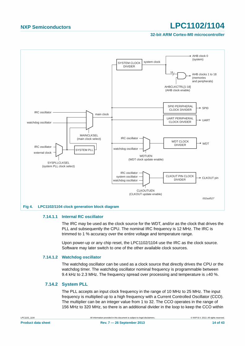
7.14 Clocking and power control
7.14.1 Crystal oscillators
The LPC1102/1104 include two independent oscillators. These are the Internal RC oscillator (IRC) and the Watchdog oscillator. Each oscillator can be used for more than one purpose as required in a particular application.
Following reset, the LPC1102/1104 operate from the Internal RC oscillator until switched by software. This allows systems to operate without any external crystal and the bootloader code to operate at a known frequency.
See Figure 4 for an overview of the LPC1102/1104 clock generation.
LPC1102_1104 All information provided in this document is subject to legal disclaimers. © NXP B.V. 2013. All rights reserved.
Product data sheet Rev. 7 — 26 September 2013 13 of 43
NXP Semiconductors LPC1102/1104 32-bit ARM Cortex-M0 microcontroller
7.14.1.1 Internal RC oscillator
The IRC may be used as the clock source for the WDT, and/or as the clock that drives the PLL and subsequently the CPU. The nominal IRC frequency is 12 MHz. The IRC is trimmed to 1 % accuracy over the entire voltage and temperature range.
Upon power-up or any chip reset, the LPC1102/1104 use the IRC as the clock source. Software may later switch to one of the other available clock sources.
7.14.1.2 Watchdog oscillator
The watchdog oscillator can be used as a clock source that directly drives the CPU or the watchdog timer. The watchdog oscillator nominal frequency is programmable between 9.4 kHz to 2.3 MHz. The frequency spread over processing and temperature is 40 %.
7.14.2 System PLL
The PLL accepts an input clock frequency in the range of 10 MHz to 25 MHz. The input frequency is multiplied up to a high frequency with a Current Controlled Oscillator (CCO). The multiplier can be an integer value from 1 to 32. The CCO operates in the range of 156 MHz to 320 MHz, so there is an additional divider in the loop to keep the CCO within
Fig 4. LPC1102/1104 clock generation block diagram
SYSTEM PLLIRC oscillator
external clockwatchdog oscillator
IRC oscillator
watchdog oscillator
MAINCLKSEL(main clock select)
SYSPLLCLKSEL(system PLL clock select)
SYSTEM CLOCKDIVIDER
AHB clock 0(system)
AHBCLKCTRL[1:18](AHB clock enable)
AHB clocks 1 to 18(memoriesand peripherals)
SPI0 PERIPHERALCLOCK DIVIDER SPI0
UART PERIPHERALCLOCK DIVIDER UART
WDT CLOCKDIVIDER WDT
WDTUEN(WDT clock update enable)
002aaf527
main clock
system clock
IRC oscillator
18
watchdog oscillator
IRC oscillatorsystem oscillator CLKOUT PIN CLOCK
DIVIDER CLKOUT pin
CLKOUTUEN(CLKOUT update enable)
LPC1102_1104 All information provided in this document is subject to legal disclaimers. © NXP B.V. 2013. All rights reserved.
Product data sheet Rev. 7 — 26 September 2013 14 of 43
NXP Semiconductors LPC1102/1104 32-bit ARM Cortex-M0 microcontroller
its frequency range while the PLL is providing the desired output frequency. The PLL output frequency must be lower than 100 MHz. The output divider may be set to divide by 2, 4, 8, or 16 to produce the output clock. Since the minimum output divider value is 2, it is insured that the PLL output has a 50 % duty cycle. The PLL is turned off and bypassed following a chip reset and may be enabled by software. The program must configure and activate the PLL, wait for the PLL to lock, and then connect to the PLL as a clock source. The PLL settling time is 100 s.
7.14.3 Clock output (LPC1104 only)
The LPC1104 features a clock output function that routes the IRC oscillator, the system oscillator, the watchdog oscillator, or the main clock to an output pin.
7.14.4 Wake-up process
The LPC1102/1104 begin operation at power-up by using the 12 MHz IRC oscillator as the clock source. This allows chip operation to resume quickly. If an external clock or the PLL is needed by the application, software will need to enable these features and wait for them to stabilize before they are used as a clock source.
7.14.5 Power control
The LPC1102/1104 support a variety of power control features. There are two special modes of processor power reduction: Sleep mode and Deep-sleep mode. The CPU clock rate may also be controlled as needed by changing clock sources, reconfiguring PLL values, and/or altering the CPU clock divider value. This allows a trade-off of power versus processing speed based on application requirements. In addition, a register is provided for shutting down the clocks to individual on-chip peripherals, allowing fine tuning of power consumption by eliminating all dynamic power use in any peripherals that are not required for the application. Selected peripherals have their own clock divider which provides even better power control.
7.14.5.1 Power profiles
The power consumption in Active and Sleep modes can be optimized for the application through a simple call to the power profiles. The power configuration routine configures the LPC1102/1104 for one of the following power modes:
• Default mode corresponding to power configuration after reset.
• CPU performance mode corresponding to optimized processing capability.
• Efficiency mode corresponding to optimized balance of current consumption and CPU performance.
• Low-current mode corresponding to lowest power consumption.
In addition, the power profiles includes a routine to select the optimal PLL settings for a given system clock and PLL input clock.
7.14.5.2 Sleep mode
When Sleep mode is entered, the clock to the core is stopped. Resumption from the Sleep mode does not need any special sequence but re-enabling the clock to the ARM core.
LPC1102_1104 All information provided in this document is subject to legal disclaimers. © NXP B.V. 2013. All rights reserved.
Product data sheet Rev. 7 — 26 September 2013 15 of 43
NXP Semiconductors LPC1102/1104 32-bit ARM Cortex-M0 microcontroller
In Sleep mode, execution of instructions is suspended until either a reset or interrupt occurs. Peripheral functions continue operation during Sleep mode and may generate interrupts to cause the processor to resume execution. Sleep mode eliminates dynamic power used by the processor itself, memory systems and related controllers, and internal buses.
7.14.5.3 Deep-sleep mode
In Deep-sleep mode, the chip is in Sleep mode, and in addition all analog blocks are shut down except for the watchdog oscillator and the BOD circuit, which can be configured to remain running in Deep-sleep mode to allow a reset initiated by a timer or BOD event. Deep-sleep mode allows for additional power savings.
Six of the GPIO pins (see Table 3) serve as external wake-up pins to a dedicated start logic to wake up the chip from Deep-sleep mode.
The clock source should be switched to IRC before entering Deep-sleep mode unless the watchdog oscillator remains running in Deep-sleep mode. The IRC can be switched on and off glitch-free and provides a clean clock signal after start-up.
7.15 System control
7.15.1 Start logic
The start logic connects external pins to corresponding interrupts in the NVIC. Each pin shown in Table 3 as input to the start logic has an individual interrupt in the NVIC interrupt vector table. The start logic pins can serve as external interrupt pins when the chip is running. In addition, an input signal on the start logic pins can wake up the chip from Deep-sleep mode when all clocks are shut down.
The start logic must be configured in the system configuration block and in the NVIC before being used.
7.15.2 Reset
Reset has four sources on the LPC1102/1104: the RESET pin, the Watchdog reset, Power-On Reset (POR), and the BrownOut Detection (BOD) circuit. In addition, there is an ARM software reset. The RESET pin is a Schmitt trigger input pin. Assertion of chip reset by any source, once the operating voltage attains a usable level, starts the IRC and initializes the flash controller.
A LOW-going pulse as short as 50 ns resets the part.
When the internal Reset is removed, the processor begins executing at address 0, which is initially the Reset vector mapped from the boot block. At that point, all of the processor and peripheral registers have been initialized to predetermined values.
7.15.3 Brownout detection
The LPC1102/1104 include up to four levels for monitoring the voltage on the VDD pin. If this voltage falls below one of the three selected levels, the BOD asserts an interrupt signal to the NVIC. This signal can be enabled for interrupt in the Interrupt Enable Register in the NVIC in order to cause a CPU interrupt; if not, software can monitor the signal by reading a dedicated status register. Four additional threshold levels can be selected to cause a forced reset of the chip.
LPC1102_1104 All information provided in this document is subject to legal disclaimers. © NXP B.V. 2013. All rights reserved.
Product data sheet Rev. 7 — 26 September 2013 16 of 43
NXP Semiconductors LPC1102/1104 32-bit ARM Cortex-M0 microcontroller
7.15.4 Code security (Code Read Protection - CRP)
This feature of the LPC1102/1104 allow user to enable different levels of security in the system so that access to the on-chip flash and use of the Serial Wire Debugger (SWD) can be restricted. When needed, CRP is invoked by programming a specific pattern into a dedicated flash location. IAP commands are not affected by the CRP.
There are three levels of Code Read Protection:
1. CRP1 disables access to the chip via the SWD and allows partial flash update (excluding flash sector 0). This mode is useful when CRP is required and flash field updates are needed but all sectors can not be erased.
2. CRP2 disables access to the chip via the SWD and only allows full flash erase and update.
3. Running an application with level CRP3 selected fully disables any access to the chip via the SWD pins.
Remark: The LPC1102 does not provide an ISP entry pin to be monitored at reset. For all three CRP levels, the user’s application code must provide a flash update mechanism which reinvokes ISP by defining a user-selected PIOn pin for ISP entry.
7.15.5 APB interface
The APB peripherals are located on one APB bus.
7.15.6 AHBLite
The AHBLite connects the CPU bus of the ARM Cortex-M0 to the flash memory, the main static RAM, and the Boot ROM.
7.15.7 External interrupt inputs
All GPIO pins can be level or edge sensitive interrupt inputs. In addition, start logic inputs serve as external interrupts (see Section 7.15.1).
7.16 Emulation and debugging
Debug functions are integrated into the ARM Cortex-M0. Serial wire debug with four breakpoints and two watchpoints is supported.
Remark: Care must be taken when using the SPI because the SPI clock SCK and the serial wire debug clock SWCLK share the same pin on the WLCSP16 package. Once the SPI is enabled, the serial wire debugger is no longer available (LPC1102 only).
CAUTION
If Code Read Protection of any level (CRP1, CRP2 or CRP3) is selected, no future factory testing can be performed on the device.
LPC1102_1104 All information provided in this document is subject to legal disclaimers. © NXP B.V. 2013. All rights reserved.
Product data sheet Rev. 7 — 26 September 2013 17 of 43
NXP Semiconductors LPC1102/1104 32-bit ARM Cortex-M0 microcontroller
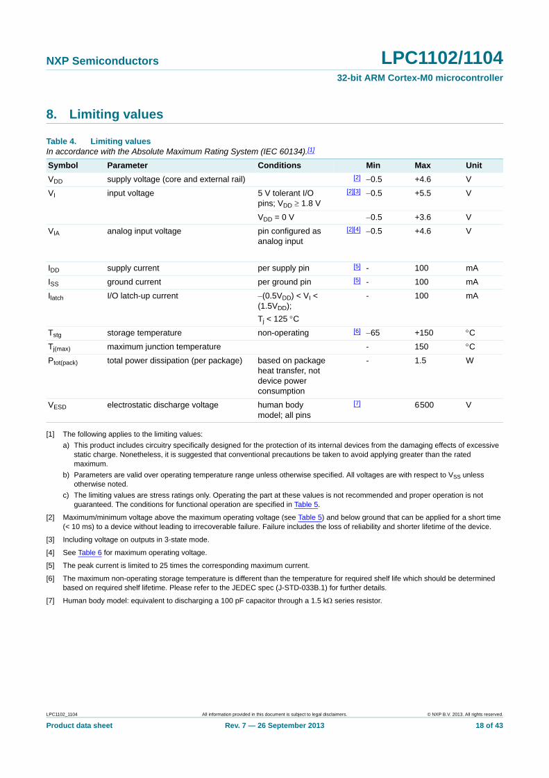
8. Limiting values
[1] The following applies to the limiting values:
a) This product includes circuitry specifically designed for the protection of its internal devices from the damaging effects of excessive static charge. Nonetheless, it is suggested that conventional precautions be taken to avoid applying greater than the rated maximum.
b) Parameters are valid over operating temperature range unless otherwise specified. All voltages are with respect to VSS unless otherwise noted.
c) The limiting values are stress ratings only. Operating the part at these values is not recommended and proper operation is not guaranteed. The conditions for functional operation are specified in Table 5.
[2] Maximum/minimum voltage above the maximum operating voltage (see Table 5) and below ground that can be applied for a short time (< 10 ms) to a device without leading to irrecoverable failure. Failure includes the loss of reliability and shorter lifetime of the device.
[3] Including voltage on outputs in 3-state mode.
[4] See Table 6 for maximum operating voltage.
[5] The peak current is limited to 25 times the corresponding maximum current.
[6] The maximum non-operating storage temperature is different than the temperature for required shelf life which should be determined based on required shelf lifetime. Please refer to the JEDEC spec (J-STD-033B.1) for further details.
[7] Human body model: equivalent to discharging a 100 pF capacitor through a 1.5 k series resistor.
Table 4. Limiting valuesIn accordance with the Absolute Maximum Rating System (IEC 60134).[1]
Symbol Parameter Conditions Min Max Unit
VDD supply voltage (core and external rail) [2] 0.5 +4.6 V
VI input voltage 5 V tolerant I/O pins; VDD 1.8 V
[2][3] 0.5 +5.5 V
VDD = 0 V 0.5 +3.6 V
VIA analog input voltage pin configured as analog input
[2][4] 0.5 +4.6 V
IDD supply current per supply pin [5] - 100 mA
ISS ground current per ground pin [5] - 100 mA
Ilatch I/O latch-up current (0.5VDD) < VI < (1.5VDD);
Tj < 125 C
- 100 mA
Tstg storage temperature non-operating [6] 65 +150 C
Tj(max) maximum junction temperature - 150 C
Ptot(pack) total power dissipation (per package) based on package heat transfer, not device power consumption
- 1.5 W
VESD electrostatic discharge voltage human body model; all pins
[7] 6500 V
LPC1102_1104 All information provided in this document is subject to legal disclaimers. © NXP B.V. 2013. All rights reserved.
Product data sheet Rev. 7 — 26 September 2013 18 of 43
NXP Semiconductors LPC1102/1104 32-bit ARM Cortex-M0 microcontroller
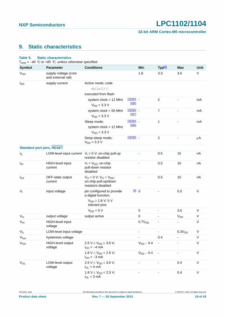
9. Static characteristics
Table 5. Static characteristicsTamb = 40 C to +85 C, unless otherwise specified.
Symbol Parameter Conditions Min Typ[1] Max Unit
VDD supply voltage (core and external rail)
1.8 3.3 3.6 V
IDD supply current Active mode; code
while(1)
executed from flash
system clock = 12 MHz
VDD = 3.3 V
[2][3][4]
[5][6]- 2 - mA
system clock = 50 MHz
VDD = 3.3 V
[2][3][5]
[6][7]- 7 - mA
Sleep mode;
system clock = 12 MHz
VDD = 3.3 V
[2][3][4]
[5][6]- 1 - mA
Deep-sleep mode; VDD = 3.3 V
[2][3][8] - 2 - A
Standard port pins, RESET
IIL LOW-level input current VI = 0 V; on-chip pull-up resistor disabled
- 0.5 10 nA
IIH HIGH-level input current
VI = VDD; on-chip pull-down resistor disabled
- 0.5 10 nA
IOZ OFF-state output current
VO = 0 V; VO = VDD; on-chip pull-up/down resistors disabled
- 0.5 10 nA
VI input voltage pin configured to provide a digital function;
VDD 1.8 V; 5 V tolerant pins
[9] 0 - 5.0 V
VDD = 0 V 0 - 3.6 V
VO output voltage output active 0 - VDD V
VIH HIGH-level input voltage
0.7VDD - - V
VIL LOW-level input voltage - - 0.3VDD V
Vhys hysteresis voltage - 0.4 - V
VOH HIGH-level output voltage
2.5 V VDD 3.6 V; IOH = 4 mA
VDD 0.4 - - V
1.8 V VDD < 2.5 V; IOH = 3 mA
VDD 0.4 - - V
VOL LOW-level output voltage
2.5 V VDD 3.6 V; IOL = 4 mA
- - 0.4 V
1.8 V VDD < 2.5 V; IOL = 3 mA
- - 0.4 V
LPC1102_1104 All information provided in this document is subject to legal disclaimers. © NXP B.V. 2013. All rights reserved.
Product data sheet Rev. 7 — 26 September 2013 19 of 43
NXP Semiconductors LPC1102/1104 32-bit ARM Cortex-M0 microcontroller
[1] Typical ratings are not guaranteed. The values listed are at room temperature (25 C), nominal supply voltages.
[2] Tamb = 25 C.
[3] IDD measurements were performed with all pins configured as GPIO outputs driven LOW and pull-up resistors disabled.
[4] IRC enabled; external clock disabled; system PLL disabled.
[5] BOD disabled.
[6] All peripherals disabled in the SYSAHBCLKCTRL register. Peripheral clocks to UART and SPI0/1 disabled in system configuration block. Low-current mode PWR_LOW_CURRENT selected when running the set_power routine in the power profiles.
[7] IRC disabled; system oscillator enabled; system PLL enabled.
[8] All oscillators and analog blocks turned off in the PDSLEEPCFG register; PDSLEEPCFG = 0x0000 18FF. Before entering deep-sleep mode, you must write a 0 to bit 4 and bit 5 of the GPIO0DATA register at location 0x5000 3FFC and a 1 to bit 4 and bit 5 of the GPIO0DIR register at location 0x5000 8000.
[9] Including voltage on outputs in 3-state mode.
[10] VDD supply voltage must be present.
[11] Allowed as long as the current limit does not exceed the maximum current allowed by the device.
IOH HIGH-level output current
VOH = VDD 0.4 V;
2.5 V VDD 3.6 V
4 - - mA
1.8 V VDD < 2.5 V 3 - - mA
IOL LOW-level output current
VOL = 0.4 V
2.5 V VDD 3.6 V
4 - - mA
1.8 V VDD < 2.5 V 3 - - mA
IOHS HIGH-level short-circuit output current
VOH = 0 V [11] - - 45 mA
IOLS LOW-level short-circuit output current
VOL = VDD[11] - - 50 mA
Ipd pull-down current VI = 5 V 10 50 150 A
Ipu pull-up current VI = 0 V;
2.0 V VDD 3.6 V
15 50 85 A
1.8 V VDD < 2.0 V 10 50 85 A
VDD < VI < 5 V 0 0 0 A
External clock input
Vi(xtal) crystal input voltage 0.5 1.8 1.95 V
Table 5. Static characteristics …continuedTamb = 40 C to +85 C, unless otherwise specified.
Symbol Parameter Conditions Min Typ[1] Max Unit
LPC1102_1104 All information provided in this document is subject to legal disclaimers. © NXP B.V. 2013. All rights reserved.
Product data sheet Rev. 7 — 26 September 2013 20 of 43
NXP Semiconductors LPC1102/1104 32-bit ARM Cortex-M0 microcontroller
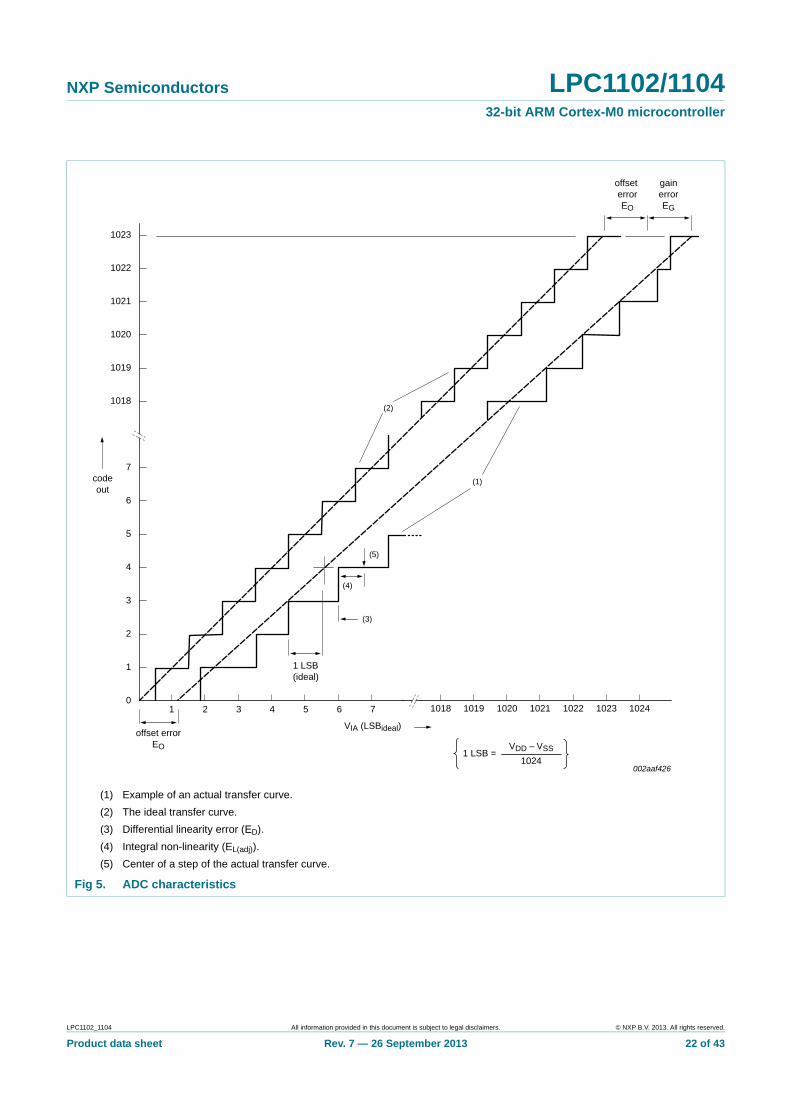
[1] The ADC is monotonic, there are no missing codes.
[2] The differential linearity error (ED) is the difference between the actual step width and the ideal step width. See Figure 5.
[3] The integral non-linearity (EL(adj)) is the peak difference between the center of the steps of the actual and the ideal transfer curve after appropriate adjustment of gain and offset errors. See Figure 5.
[4] The offset error (EO) is the absolute difference between the straight line which fits the actual curve and the straight line which fits the ideal curve. See Figure 5.
[5] The gain error (EG) is the relative difference in percent between the straight line fitting the actual transfer curve after removing offset error, and the straight line which fits the ideal transfer curve. See Figure 5.
[6] The absolute error (ET) is the maximum difference between the center of the steps of the actual transfer curve of the non-calibrated ADC and the ideal transfer curve. See Figure 5.
[7] Tamb = 25 C; maximum sampling frequency fs = 400 kSamples/s and analog input capacitance Cia = 1 pF.
[8] Input resistance Ri depends on the sampling frequency fs: Ri = 1 / (fs Cia).
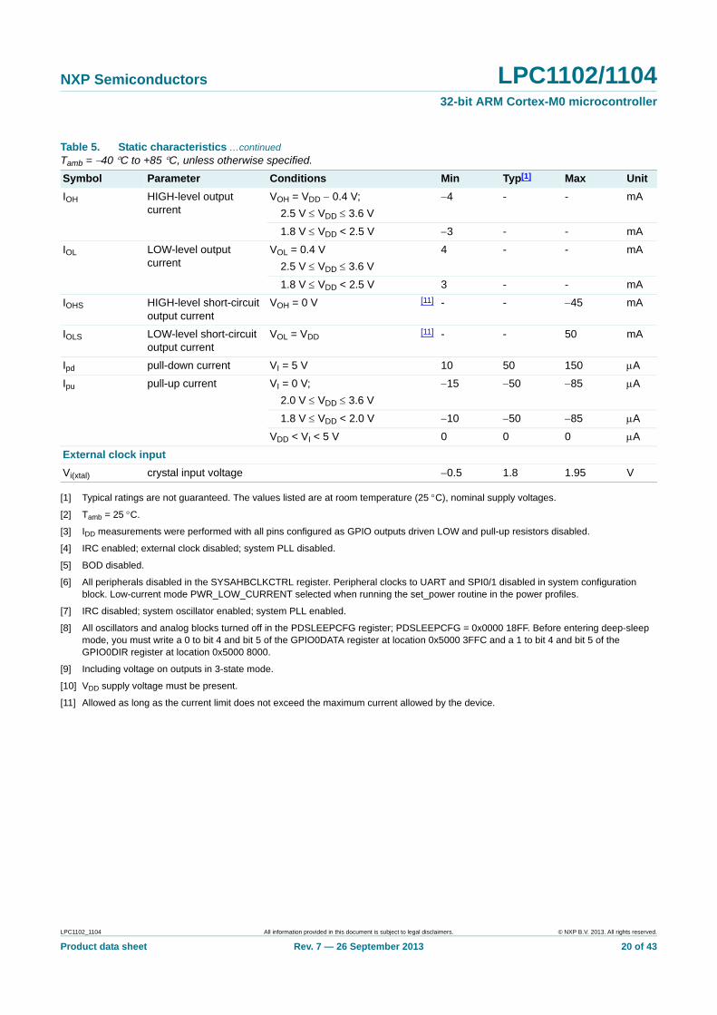
Table 6. ADC static characteristicsTamb = 40 C to +85 C unless otherwise specified; ADC frequency 4.5 MHz, VDD = 2.5 V to 3.6 V.
Symbol Parameter Conditions Min Typ Max Unit
VIA analog input voltage 0 - VDD V
Cia analog input capacitance - - 1 pF
ED differential linearity error [1][2] - - 1 LSB
EL(adj) integral non-linearity [3] - - 1.5 LSB
EO offset error [4] - - 3.5 LSB
EG gain error [5] - - 0.6 %
ET absolute error [6] - - 4 LSB
Rvsi voltage source interface resistance
- - 40 k
Ri input resistance [7][8] - - 2.5 M
LPC1102_1104 All information provided in this document is subject to legal disclaimers. © NXP B.V. 2013. All rights reserved.
Product data sheet Rev. 7 — 26 September 2013 21 of 43
NXP Semiconductors LPC1102/1104 32-bit ARM Cortex-M0 microcontroller
(1) Example of an actual transfer curve.
(2) The ideal transfer curve.
(3) Differential linearity error (ED).
(4) Integral non-linearity (EL(adj)).
(5) Center of a step of the actual transfer curve.
Fig 5. ADC characteristics
002aaf426
1023
1022
1021
1020
1019
(2)
(1)
10241018 1019 1020 1021 1022 102371 2 3 4 5 6
7
6
5
4
3
2
1
0
1018
(5)
(4)
(3)
1 LSB(ideal)
codeout
VDD − VSS
1024
offset errorEO
gainerrorEG
offset errorEO
VIA (LSBideal)
1 LSB =
LPC1102_1104 All information provided in this document is subject to legal disclaimers. © NXP B.V. 2013. All rights reserved.
Product data sheet Rev. 7 — 26 September 2013 22 of 43
NXP Semiconductors LPC1102/1104 32-bit ARM Cortex-M0 microcontroller
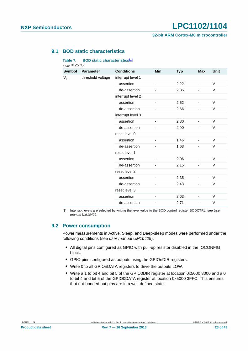
9.1 BOD static characteristics
[1] Interrupt levels are selected by writing the level value to the BOD control register BODCTRL, see User manual UM10429.
9.2 Power consumption
Power measurements in Active, Sleep, and Deep-sleep modes were performed under the following conditions (see user manual UM10429):
• All digital pins configured as GPIO with pull-up resistor disabled in the IOCONFIG block.
• GPIO pins configured as outputs using the GPIOnDIR registers.
• Write 0 to all GPIOnDATA registers to drive the outputs LOW.
• Write a 1 to bit 4 and bit 5 of the GPIO0DIR register at location 0x5000 8000 and a 0 to bit 4 and bit 5 of the GPIO0DATA register at location 0x5000 3FFC. This ensures that not-bonded out pins are in a well-defined state.
Table 7. BOD static characteristics[1]
Tamb = 25 C.
Symbol Parameter Conditions Min Typ Max Unit
Vth threshold voltage interrupt level 1
assertion - 2.22 - V
de-assertion - 2.35 - V
interrupt level 2
assertion - 2.52 - V
de-assertion - 2.66 - V
interrupt level 3
assertion - 2.80 - V
de-assertion - 2.90 - V
reset level 0
assertion - 1.46 - V
de-assertion - 1.63 - V
reset level 1
assertion - 2.06 - V
de-assertion - 2.15 - V
reset level 2
assertion - 2.35 - V
de-assertion - 2.43 - V
reset level 3
assertion - 2.63 - V
de-assertion - 2.71 - V
LPC1102_1104 All information provided in this document is subject to legal disclaimers. © NXP B.V. 2013. All rights reserved.
Product data sheet Rev. 7 — 26 September 2013 23 of 43
NXP Semiconductors LPC1102/1104 32-bit ARM Cortex-M0 microcontroller
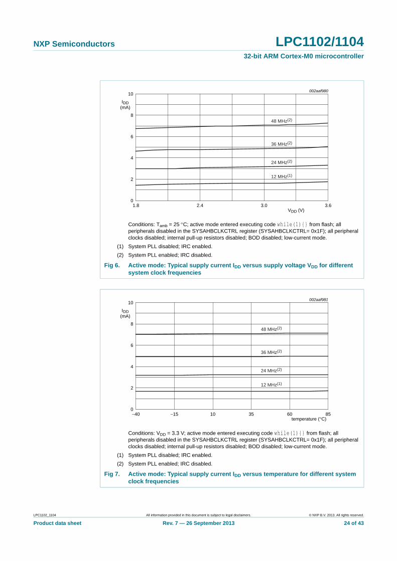
Conditions: Tamb = 25 C; active mode entered executing code while(1) from flash; all peripherals disabled in the SYSAHBCLKCTRL register (SYSAHBCLKCTRL= 0x1F); all peripheral clocks disabled; internal pull-up resistors disabled; BOD disabled; low-current mode.
(1) System PLL disabled; IRC enabled.
(2) System PLL enabled; IRC disabled.
Fig 6. Active mode: Typical supply current IDD versus supply voltage VDD for different system clock frequencies
Conditions: VDD = 3.3 V; active mode entered executing code while(1) from flash; all peripherals disabled in the SYSAHBCLKCTRL register (SYSAHBCLKCTRL= 0x1F); all peripheral clocks disabled; internal pull-up resistors disabled; BOD disabled; low-current mode.
(1) System PLL disabled; IRC enabled.
(2) System PLL enabled; IRC disabled.
Fig 7. Active mode: Typical supply current IDD versus temperature for different system clock frequencies
VDD (V)1.8 3.63.02.4
002aaf980
4
6
2
8
10
IDD(mA)
0
12 MHz(1)
24 MHz(2)
36 MHz(2)
48 MHz(2)
002aaf981
temperature (°C)−40 853510 60−15
2
8
6
4
10
IDD(mA)
0
12 MHz(1)
24 MHz(2)
36 MHz(2)
48 MHz(2)
LPC1102_1104 All information provided in this document is subject to legal disclaimers. © NXP B.V. 2013. All rights reserved.
Product data sheet Rev. 7 — 26 September 2013 24 of 43
NXP Semiconductors LPC1102/1104 32-bit ARM Cortex-M0 microcontroller
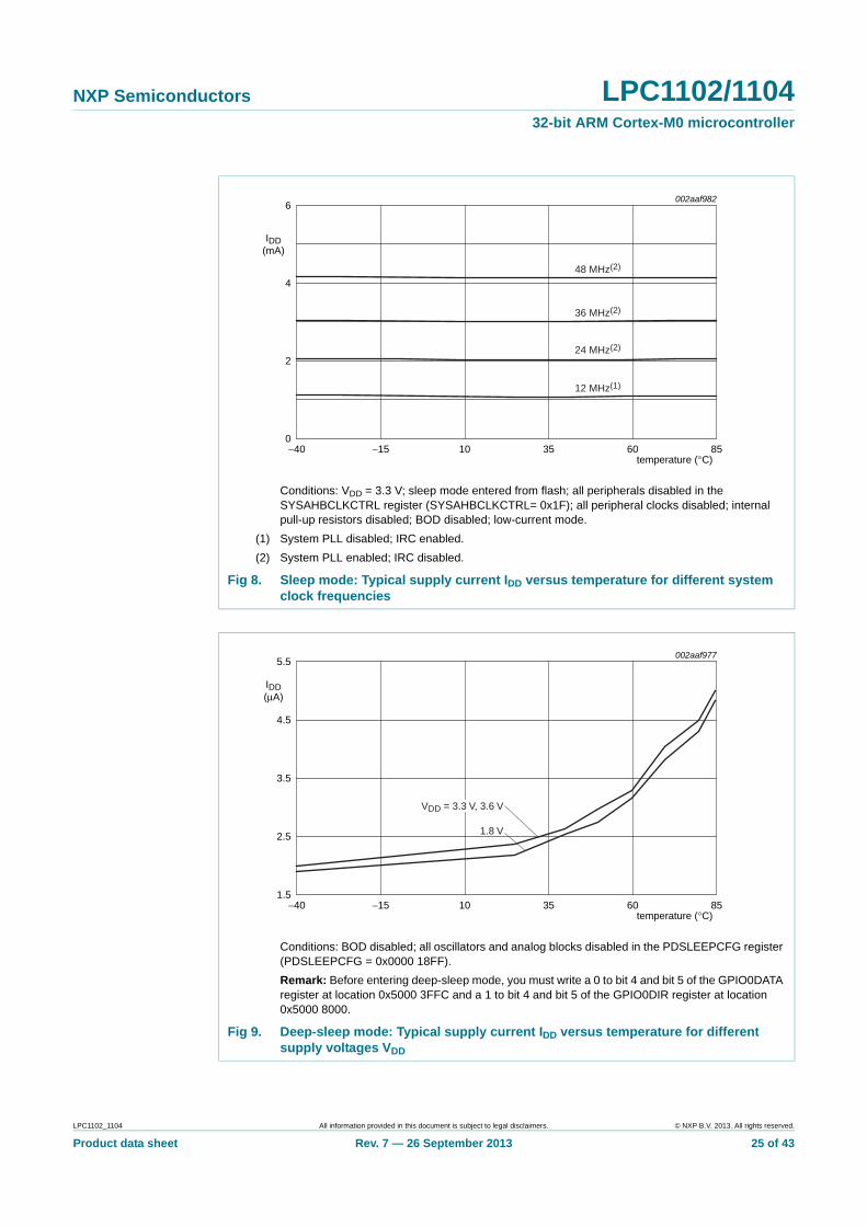
Conditions: VDD = 3.3 V; sleep mode entered from flash; all peripherals disabled in the SYSAHBCLKCTRL register (SYSAHBCLKCTRL= 0x1F); all peripheral clocks disabled; internal pull-up resistors disabled; BOD disabled; low-current mode.
(1) System PLL disabled; IRC enabled.
(2) System PLL enabled; IRC disabled.
Fig 8. Sleep mode: Typical supply current IDD versus temperature for different system clock frequencies
Conditions: BOD disabled; all oscillators and analog blocks disabled in the PDSLEEPCFG register (PDSLEEPCFG = 0x0000 18FF).
Remark: Before entering deep-sleep mode, you must write a 0 to bit 4 and bit 5 of the GPIO0DATA register at location 0x5000 3FFC and a 1 to bit 4 and bit 5 of the GPIO0DIR register at location 0x5000 8000.
Fig 9. Deep-sleep mode: Typical supply current IDD versus temperature for different supply voltages VDD
temperature (°C)−40 853510 60−15
002aaf982
2
4
6
IDD(mA)
0
12 MHz(1)
24 MHz(2)
36 MHz(2)
48 MHz(2)
002aaf977
temperature (°C)−40 853510 60−15
2.5
4.5
3.5
5.5
IDD(μA)
1.5
VDD = 3.3 V, 3.6 V
1.8 V
LPC1102_1104 All information provided in this document is subject to legal disclaimers. © NXP B.V. 2013. All rights reserved.
Product data sheet Rev. 7 — 26 September 2013 25 of 43
NXP Semiconductors LPC1102/1104 32-bit ARM Cortex-M0 microcontroller
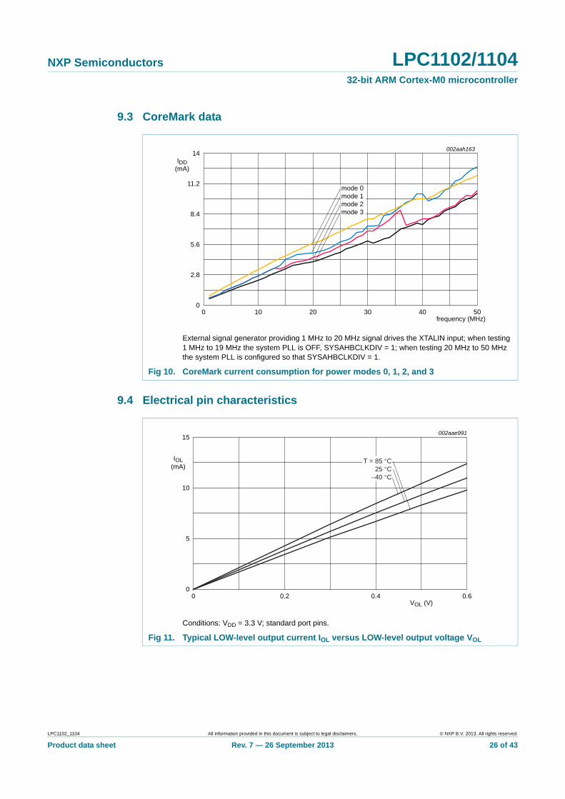
9.3 CoreMark data
9.4 Electrical pin characteristics
External signal generator providing 1 MHz to 20 MHz signal drives the XTALIN input; when testing 1 MHz to 19 MHz the system PLL is OFF, SYSAHBCLKDIV = 1; when testing 20 MHz to 50 MHz the system PLL is configured so that SYSAHBCLKDIV = 1.
Fig 10. CoreMark current consumption for power modes 0, 1, 2, and 3
002aah163
0 10 20 30 40 500
2.8
5.6
8.4
11.2
14
frequency (MHz)
IDD(mA)
mode 0mode 1mode 2mode 3
Conditions: VDD = 3.3 V; standard port pins.
Fig 11. Typical LOW-level output current IOL versus LOW-level output voltage VOL
VOL (V)0 0.60.40.2
002aae991
5
10
15
IOL(mA)
0
T = 85 °C25 °C
−40 °C
LPC1102_1104 All information provided in this document is subject to legal disclaimers. © NXP B.V. 2013. All rights reserved.
Product data sheet Rev. 7 — 26 September 2013 26 of 43
NXP Semiconductors LPC1102/1104 32-bit ARM Cortex-M0 microcontroller
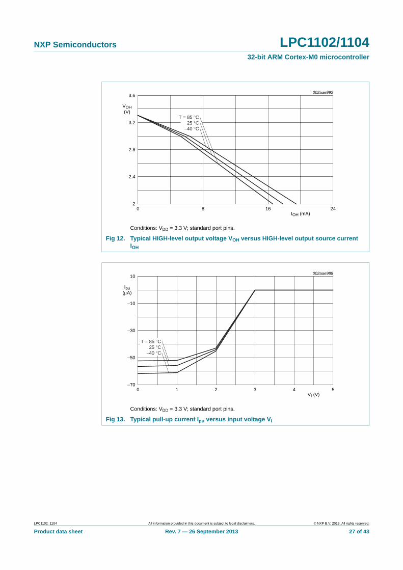
Conditions: VDD = 3.3 V; standard port pins.
Fig 12. Typical HIGH-level output voltage VOH versus HIGH-level output source current IOH
Conditions: VDD = 3.3 V; standard port pins.
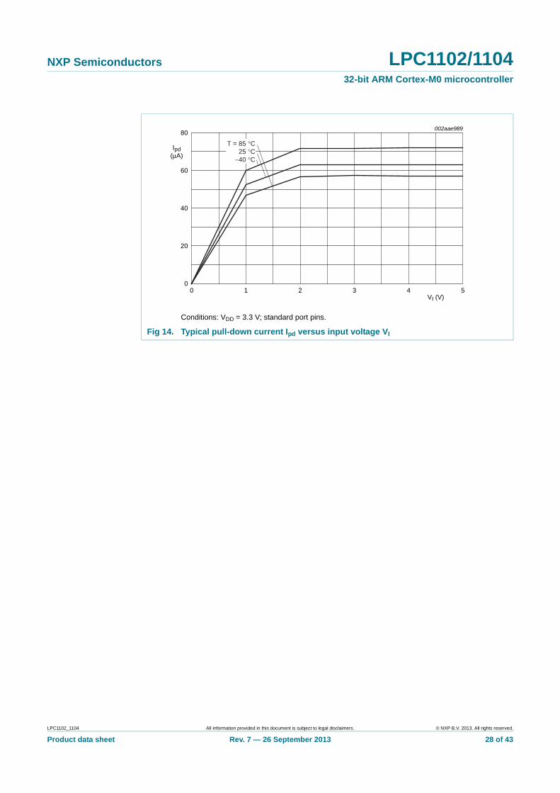
Fig 13. Typical pull-up current Ipu versus input voltage VI
IOH (mA)0 24168
002aae992
2.8
2.4
3.2
3.6
VOH(V)
2
T = 85 °C25 °C
−40 °C
VI (V)0 542 31
002aae988
−30
−50
−10
10
Ipu(μA)
−70
T = 85 °C25 °C
−40 °C
LPC1102_1104 All information provided in this document is subject to legal disclaimers. © NXP B.V. 2013. All rights reserved.
Product data sheet Rev. 7 — 26 September 2013 27 of 43
NXP Semiconductors LPC1102/1104 32-bit ARM Cortex-M0 microcontroller
Conditions: VDD = 3.3 V; standard port pins.
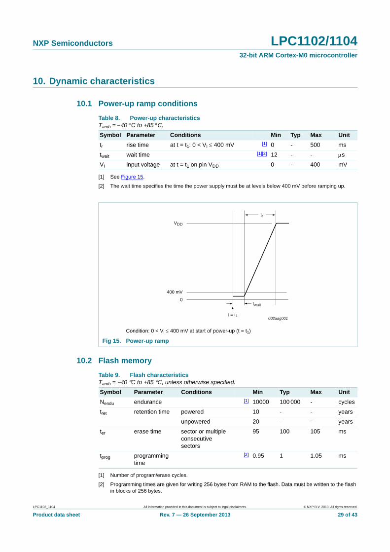
Fig 14. Typical pull-down current Ipd versus input voltage VI
VI (V)0 542 31
002aae989
40
20
60
80
Ipd(μA)
0
T = 85 °C25 °C
−40 °C
LPC1102_1104 All information provided in this document is subject to legal disclaimers. © NXP B.V. 2013. All rights reserved.
Product data sheet Rev. 7 — 26 September 2013 28 of 43
NXP Semiconductors LPC1102/1104 32-bit ARM Cortex-M0 microcontroller
10. Dynamic characteristics
10.1 Power-up ramp conditions
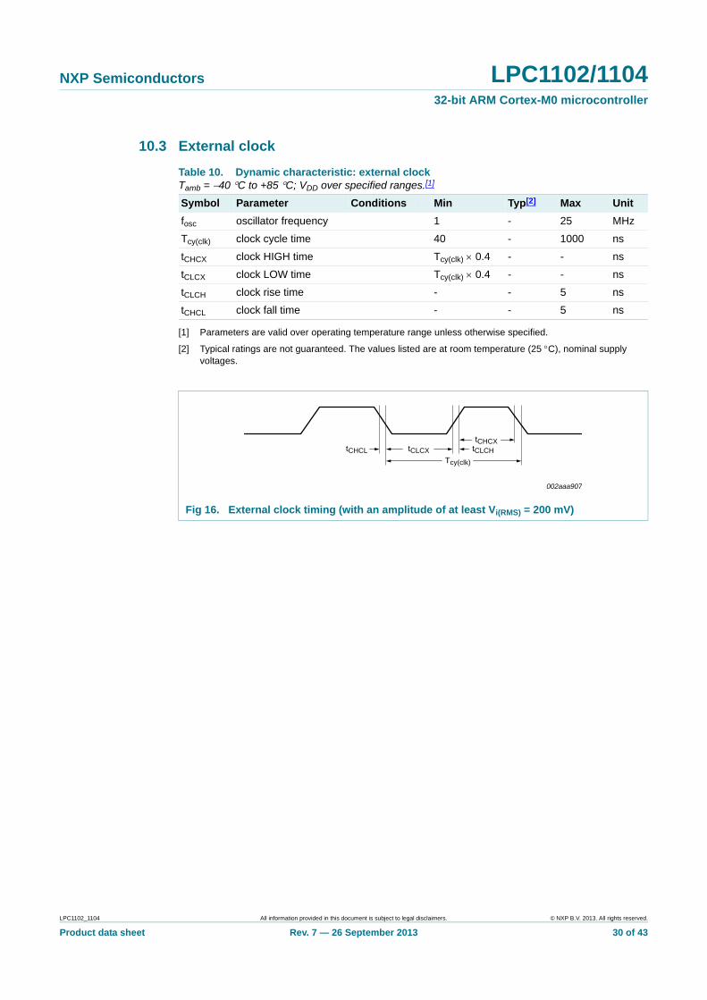
[1] See Figure 15.
[2] The wait time specifies the time the power supply must be at levels below 400 mV before ramping up.
10.2 Flash memory
[1] Number of program/erase cycles.
[2] Programming times are given for writing 256 bytes from RAM to the flash. Data must be written to the flash in blocks of 256 bytes.
Table 8. Power-up characteristicsTamb = 40 C to +85 C.
Symbol Parameter Conditions Min Typ Max Unit
tr rise time at t = t1: 0 < VI 400 mV [1] 0 - 500 ms
twait wait time [1][2] 12 - - s
VI input voltage at t = t1 on pin VDD 0 - 400 mV
Condition: 0 < VI 400 mV at start of power-up (t = t1)
Fig 15. Power-up ramp
VDD
0
400 mV
tr
twait
t = t1002aag001
Table 9. Flash characteristicsTamb = 40 C to +85 C, unless otherwise specified.
Symbol Parameter Conditions Min Typ Max Unit
Nendu endurance [1] 10000 100 000 - cycles
tret retention time powered 10 - - years
unpowered 20 - - years
ter erase time sector or multiple consecutive sectors
95 100 105 ms
tprog programming time
[2] 0.95 1 1.05 ms
LPC1102_1104 All information provided in this document is subject to legal disclaimers. © NXP B.V. 2013. All rights reserved.
Product data sheet Rev. 7 — 26 September 2013 29 of 43
NXP Semiconductors LPC1102/1104 32-bit ARM Cortex-M0 microcontroller
10.3 External clock
[1] Parameters are valid over operating temperature range unless otherwise specified.
[2] Typical ratings are not guaranteed. The values listed are at room temperature (25 C), nominal supply voltages.
Table 10. Dynamic characteristic: external clockTamb = 40 C to +85 C; VDD over specified ranges.[1]
Symbol Parameter Conditions Min Typ[2] Max Unit
fosc oscillator frequency 1 - 25 MHz
Tcy(clk) clock cycle time 40 - 1000 ns
tCHCX clock HIGH time Tcy(clk) 0.4 - - ns
tCLCX clock LOW time Tcy(clk) 0.4 - - ns
tCLCH clock rise time - - 5 ns
tCHCL clock fall time - - 5 ns
Fig 16. External clock timing (with an amplitude of at least Vi(RMS) = 200 mV)
tCHCL tCLCX
tCHCX
Tcy(clk)
tCLCH
002aaa907
LPC1102_1104 All information provided in this document is subject to legal disclaimers. © NXP B.V. 2013. All rights reserved.
Product data sheet Rev. 7 — 26 September 2013 30 of 43
NXP Semiconductors LPC1102/1104 32-bit ARM Cortex-M0 microcontroller
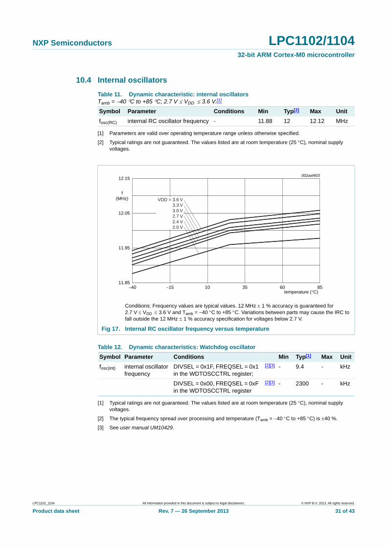
10.4 Internal oscillators
[1] Parameters are valid over operating temperature range unless otherwise specified.
[2] Typical ratings are not guaranteed. The values listed are at room temperature (25 C), nominal supply voltages.
[1] Typical ratings are not guaranteed. The values listed are at room temperature (25 C), nominal supply voltages.
[2] The typical frequency spread over processing and temperature (Tamb = 40 C to +85 C) is 40 %.
[3] See user manual UM10429.
Table 11. Dynamic characteristic: internal oscillatorsTamb = 40 C to +85 C; 2.7 V VDD 3.6 V.[1]
Symbol Parameter Conditions Min Typ[2] Max Unit
fosc(RC) internal RC oscillator frequency - 11.88 12 12.12 MHz
Conditions: Frequency values are typical values. 12 MHz 1 % accuracy is guaranteed for 2.7 V VDD 3.6 V and Tamb = 40 C to +85 C. Variations between parts may cause the IRC to fall outside the 12 MHz 1 % accuracy specification for voltages below 2.7 V.
Fig 17. Internal RC oscillator frequency versus temperature
Table 12. Dynamic characteristics: Watchdog oscillator
Symbol Parameter Conditions Min Typ[1] Max Unit
fosc(int) internal oscillator frequency
DIVSEL = 0x1F, FREQSEL = 0x1 in the WDTOSCCTRL register;
[2][3] - 9.4 - kHz
DIVSEL = 0x00, FREQSEL = 0xF in the WDTOSCCTRL register
[2][3] - 2300 - kHz
002aaf403
11.95
12.05
12.15
f(MHz)
11.85
temperature (°C)−40 853510 60−15
VDD = 3.6 V3.3 V3.0 V2.7 V2.4 V2.0 V
LPC1102_1104 All information provided in this document is subject to legal disclaimers. © NXP B.V. 2013. All rights reserved.
Product data sheet Rev. 7 — 26 September 2013 31 of 43
NXP Semiconductors LPC1102/1104 32-bit ARM Cortex-M0 microcontroller
10.5 I/O pins
[1] Applies to standard port pins and RESET pin.
10.6 SPI interfaces
[1] Tcy(clk) = (SSPCLKDIV (1 + SCR) CPSDVSR) / fmain. The clock cycle time derived from the SPI bit rate Tcy(clk) is a function of the main clock frequency fmain, the SPI peripheral clock divider (SSPCLKDIV), the SPI SCR parameter (specified in the SSP0CR0 register), and the SPI CPSDVSR parameter (specified in the SPI clock prescale register).
[2] Tamb = 40 C to 85 C.
[3] Tcy(clk) = 12 Tcy(PCLK).
[4] Tamb = 25 C; for normal voltage supply range: VDD = 3.3 V.
Table 13. Dynamic characteristic: I/O pins[1]
Tamb = 40 C to +85 C; 3.0 V VDD 3.6 V.
Symbol Parameter Conditions Min Typ Max Unit
tr rise time pin configured as output
3.0 - 5.0 ns
tf fall time pin configured as output
2.5 - 5.0 ns
Table 14. Dynamic characteristics of SPI pins in SPI mode
Symbol Parameter Conditions Min Typ Max Unit
SPI master (in SPI mode)
Tcy(clk) clock cycle time when only receiving [1] 50 - - ns
when only transmitting [1] 40 ns
tDS data set-up time in SPI mode
2.4 V VDD 3.6 V
[2] 15 - - ns
2.0 V VDD < 2.4 V [2] 20 ns
1.8 V VDD < 2.0 V [2] 24 - - ns
tDH data hold time in SPI mode [2] 0 - - ns
tv(Q) data output valid time in SPI mode [2] - - 10 ns
th(Q) data output hold time in SPI mode [2] 0 - - ns
SPI slave (in SPI mode)
Tcy(PCLK) PCLK cycle time 20 - - ns
tDS data set-up time in SPI mode [3][4] 0 - - ns
tDH data hold time in SPI mode [3][4] 3 Tcy(PCLK) + 4 - - ns
tv(Q) data output valid time in SPI mode [3][4] - - 3 Tcy(PCLK) + 11 ns
th(Q) data output hold time in SPI mode [3][4] - - 2 Tcy(PCLK) + 5 ns
LPC1102_1104 All information provided in this document is subject to legal disclaimers. © NXP B.V. 2013. All rights reserved.
Product data sheet Rev. 7 — 26 September 2013 32 of 43
NXP Semiconductors LPC1102/1104 32-bit ARM Cortex-M0 microcontroller
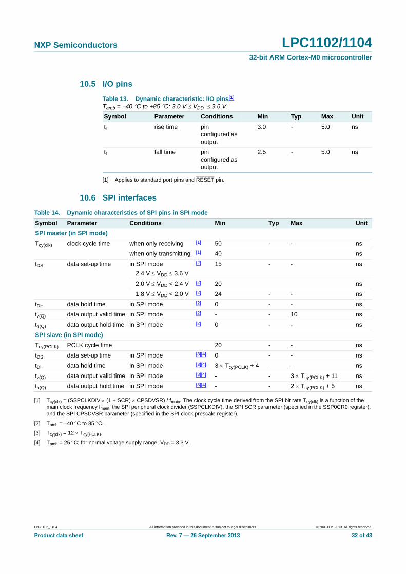
Fig 18. SPI master timing in SPI mode
SCK (CPOL = 0)
MOSI
MISO
Tcy(clk)
tDS tDH
tv(Q)
DATA VALID DATA VALID
th(Q)
SCK (CPOL = 1)
DATA VALID DATA VALID
MOSI
MISO
tDS tDH
DATA VALID DATA VALID
th(Q)
DATA VALID DATA VALID
tv(Q)
CPHA = 1
CPHA = 0
002aae829
LPC1102_1104 All information provided in this document is subject to legal disclaimers. © NXP B.V. 2013. All rights reserved.
Product data sheet Rev. 7 — 26 September 2013 33 of 43
NXP Semiconductors LPC1102/1104 32-bit ARM Cortex-M0 microcontroller
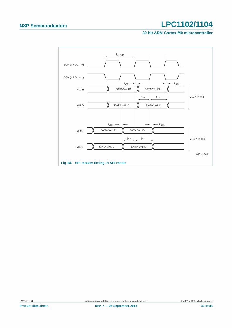
Fig 19. SPI slave timing in SPI mode
SCK (CPOL = 0)
MOSI
MISO
Tcy(clk)
tDS tDH
tv(Q)
DATA VALID DATA VALID
th(Q)
SCK (CPOL = 1)
DATA VALID DATA VALID
MOSI
MISO
tDS tDH
tv(Q)
DATA VALID DATA VALID
th(Q)
DATA VALID DATA VALID
CPHA = 1
CPHA = 0
002aae830
LPC1102_1104 All information provided in this document is subject to legal disclaimers. © NXP B.V. 2013. All rights reserved.
Product data sheet Rev. 7 — 26 September 2013 34 of 43
NXP Semiconductors LPC1102/1104 32-bit ARM Cortex-M0 microcontroller
11. Application information
11.1 ADC usage notes
The following guidelines show how to increase the performance of the ADC in a noisy environment beyond the ADC specifications listed in Table 6:
• The ADC input trace must be short and as close as possible to the LPC1102/1104 chip.
• The ADC input traces must be shielded from fast switching digital signals and noisy power supply lines.
• Because the ADC and the digital core share the same power supply, the power supply line must be adequately filtered.
• To improve the ADC performance in a very noisy environment, put the device in Sleep mode during the ADC conversion.
11.2 XTAL input
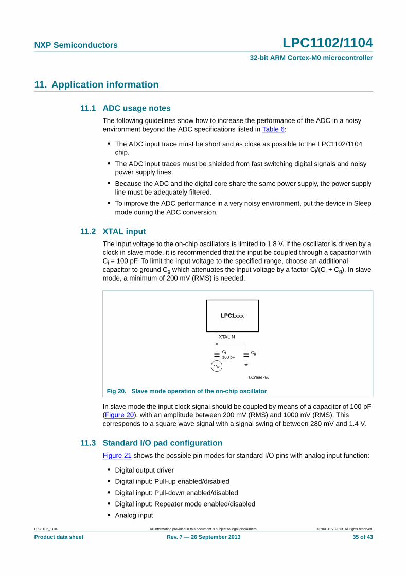
The input voltage to the on-chip oscillators is limited to 1.8 V. If the oscillator is driven by a clock in slave mode, it is recommended that the input be coupled through a capacitor with Ci = 100 pF. To limit the input voltage to the specified range, choose an additional capacitor to ground Cg which attenuates the input voltage by a factor Ci/(Ci + Cg). In slave mode, a minimum of 200 mV (RMS) is needed.
In slave mode the input clock signal should be coupled by means of a capacitor of 100 pF (Figure 20), with an amplitude between 200 mV (RMS) and 1000 mV (RMS). This corresponds to a square wave signal with a signal swing of between 280 mV and 1.4 V.
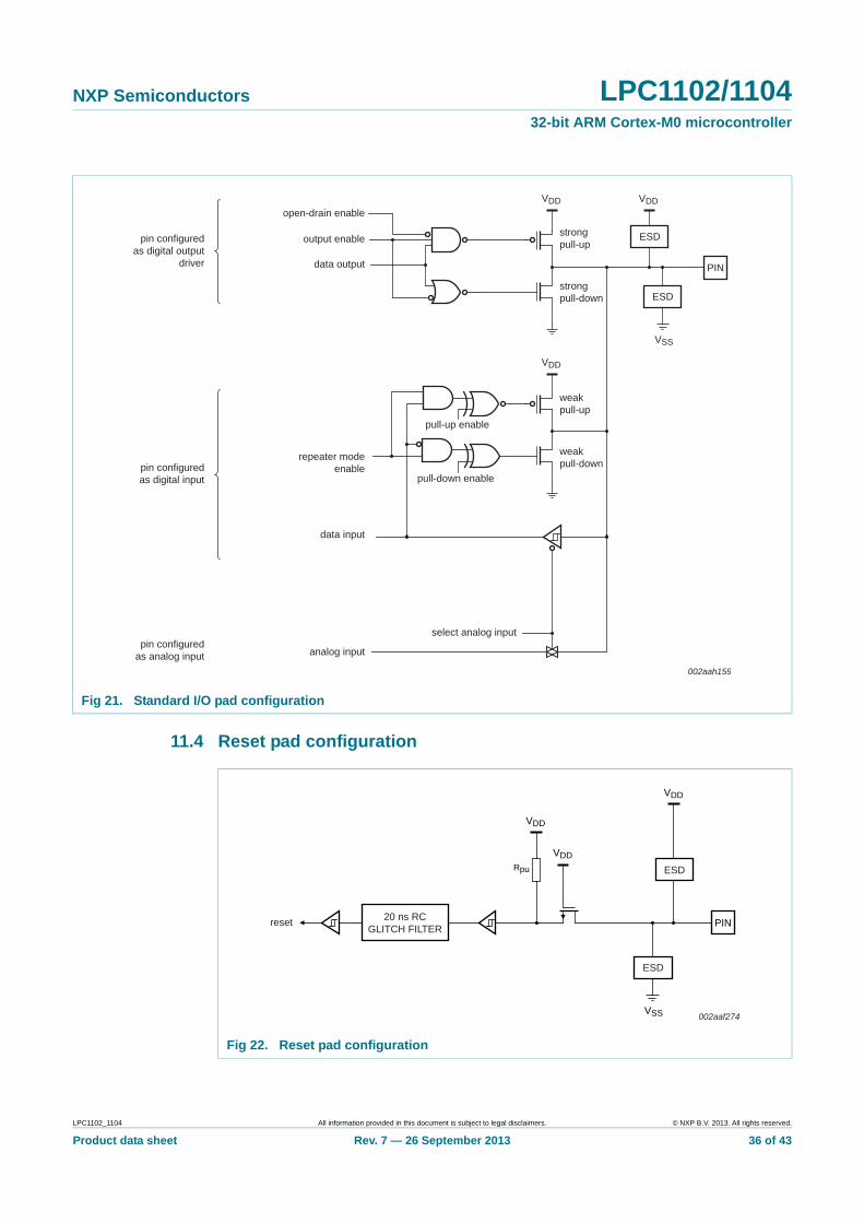
11.3 Standard I/O pad configuration
Figure 21 shows the possible pin modes for standard I/O pins with analog input function:
• Digital output driver
• Digital input: Pull-up enabled/disabled
• Digital input: Pull-down enabled/disabled
• Digital input: Repeater mode enabled/disabled
• Analog input
Fig 20. Slave mode operation of the on-chip oscillator
LPC1xxx
XTALIN
Ci100 pF
Cg
002aae788
LPC1102_1104 All information provided in this document is subject to legal disclaimers. © NXP B.V. 2013. All rights reserved.
Product data sheet Rev. 7 — 26 September 2013 35 of 43
NXP Semiconductors LPC1102/1104 32-bit ARM Cortex-M0 microcontroller
11.4 Reset pad configuration
Fig 21. Standard I/O pad configuration
PIN
VDD VDD
ESD
VSS
ESD
strongpull-up
strongpull-down
VDD
weakpull-up
weakpull-down
open-drain enable
output enable
repeater modeenable
pull-up enable
pull-down enable
data output
data input
analog input
select analog input
002aah159
pin configuredas digital output
driver
pin configuredas digital input
pin configuredas analog input
Fig 22. Reset pad configuration
VSS
reset
002aaf274
VDD
VDD
VDD
Rpu ESD
ESD
20 ns RCGLITCH FILTER
PIN
LPC1102_1104 All information provided in this document is subject to legal disclaimers. © NXP B.V. 2013. All rights reserved.
Product data sheet Rev. 7 — 26 September 2013 36 of 43
NXP Semiconductors LPC1102/1104 32-bit ARM Cortex-M0 microcontroller
11.5 ADC effective input impedance
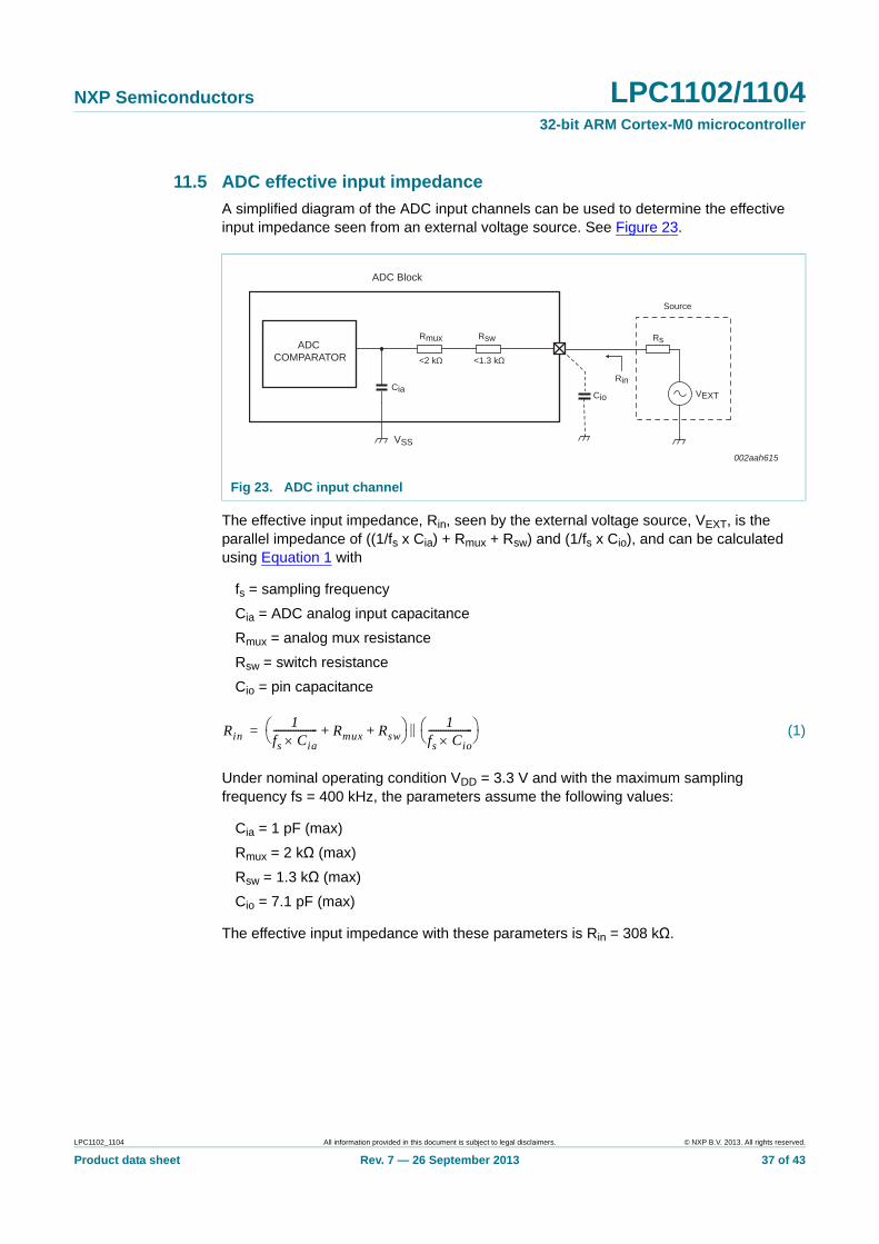
A simplified diagram of the ADC input channels can be used to determine the effective input impedance seen from an external voltage source. See Figure 23.
The effective input impedance, Rin, seen by the external voltage source, VEXT, is the parallel impedance of ((1/fs x Cia) + Rmux + Rsw) and (1/fs x Cio), and can be calculated using Equation 1 with
fs = sampling frequency
Cia = ADC analog input capacitance
Rmux = analog mux resistance
Rsw = switch resistance
Cio = pin capacitance
(1)
Under nominal operating condition VDD = 3.3 V and with the maximum sampling frequency fs = 400 kHz, the parameters assume the following values:
Cia = 1 pF (max)
Rmux = 2 kΩ (max)
Rsw = 1.3 kΩ (max)
Cio = 7.1 pF (max)
The effective input impedance with these parameters is Rin = 308 kΩ.
Fig 23. ADC input channel
Cia
Rs
VSS
VEXT
002aah615
ADC COMPARATOR
ADC Block
Rin
Cio
Rmux Rsw
Source
<2 kΩ <1.3 kΩ
Rin1
fs Cia------------------ Rmux Rsw+ + 1
fs Cio------------------ =
LPC1102_1104 All information provided in this document is subject to legal disclaimers. © NXP B.V. 2013. All rights reserved.
Product data sheet Rev. 7 — 26 September 2013 37 of 43
NXP Semiconductors LPC1102/1104 32-bit ARM Cortex-M0 microcontroller
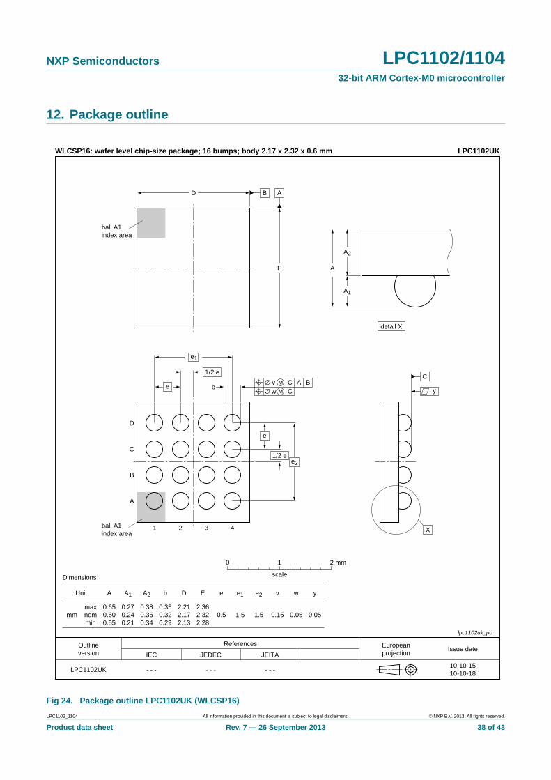
12. Package outline
Fig 24. Package outline LPC1102UK (WLCSP16)
ReferencesOutlineversion
Europeanprojection
Issue dateIEC JEDEC JEITA
LPC1102UK - - -- - -- - -
lpc1102uk_po
10-10-1510-10-18
Unit
mmmaxnommin
0.650.600.55
0.270.240.21
0.350.320.29
2.212.172.13
2.362.322.28
0.5 1.5 0.15
A
Dimensions
WLCSP16: wafer level chip-size package; 16 bumps; body 2.17 x 2.32 x 0.6 mm LPC1102UK
A1 A2
0.380.360.34
b D E e e1
1.5
e2 v w
0.05 0.05
y
0 1 2 mm
scale
ball A1index area
B AD
E
C
y
X
detail X
A
A2
A1
b
e2
e1
e
e
1/2 e
1/2 e
AC B∅ vC∅ w
ball A1index area
1 2 3 4
A
B
C
D
LPC1102_1104 All information provided in this document is subject to legal disclaimers. © NXP B.V. 2013. All rights reserved.
Product data sheet Rev. 7 — 26 September 2013 38 of 43
NXP Semiconductors LPC1102/1104 32-bit ARM Cortex-M0 microcontroller
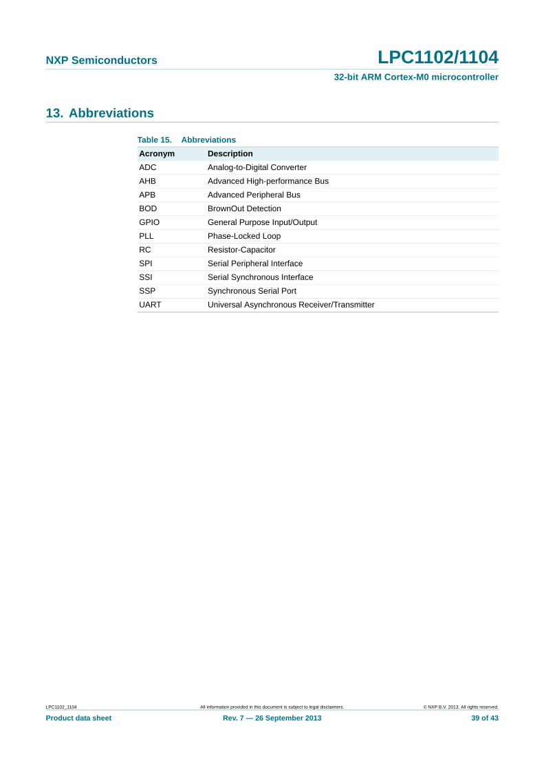
13. Abbreviations
Table 15. Abbreviations
Acronym Description
ADC Analog-to-Digital Converter
AHB Advanced High-performance Bus
APB Advanced Peripheral Bus
BOD BrownOut Detection
GPIO General Purpose Input/Output
PLL Phase-Locked Loop
RC Resistor-Capacitor
SPI Serial Peripheral Interface
SSI Serial Synchronous Interface
SSP Synchronous Serial Port
UART Universal Asynchronous Receiver/Transmitter
LPC1102_1104 All information provided in this document is subject to legal disclaimers. © NXP B.V. 2013. All rights reserved.
Product data sheet Rev. 7 — 26 September 2013 39 of 43
NXP Semiconductors LPC1102/1104 32-bit ARM Cortex-M0 microcontroller
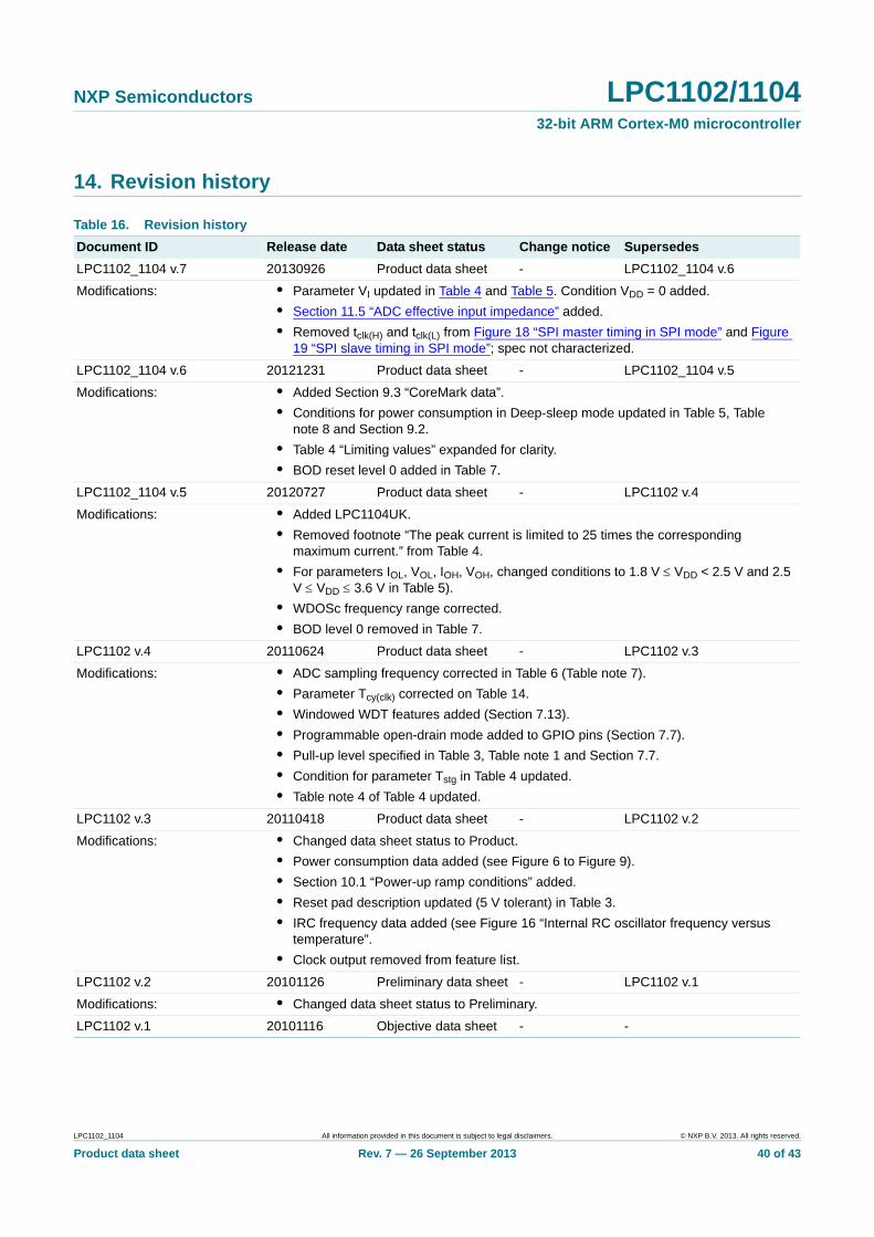
14. Revision history
Table 16. Revision history
Document ID Release date Data sheet status Change notice Supersedes
LPC1102_1104 v.7 20130926 Product data sheet - LPC1102_1104 v.6
Modifications: • Parameter VI updated in Table 4 and Table 5. Condition VDD = 0 added.
• Section 11.5 “ADC effective input impedance” added.
• Removed tclk(H) and tclk(L) from Figure 18 “SPI master timing in SPI mode” and Figure 19 “SPI slave timing in SPI mode”; spec not characterized.
LPC1102_1104 v.6 20121231 Product data sheet - LPC1102_1104 v.5
Modifications: • Added Section 9.3 “CoreMark data”.
• Conditions for power consumption in Deep-sleep mode updated in Table 5, Table note 8 and Section 9.2.
• Table 4 “Limiting values” expanded for clarity.
• BOD reset level 0 added in Table 7.
LPC1102_1104 v.5 20120727 Product data sheet - LPC1102 v.4
Modifications: • Added LPC1104UK.
• Removed footnote “The peak current is limited to 25 times the corresponding maximum current.” from Table 4.
• For parameters IOL, VOL, IOH, VOH, changed conditions to 1.8 V VDD < 2.5 V and 2.5 V VDD 3.6 V in Table 5).
• WDOSc frequency range corrected.
• BOD level 0 removed in Table 7.
LPC1102 v.4 20110624 Product data sheet - LPC1102 v.3
Modifications: • ADC sampling frequency corrected in Table 6 (Table note 7).
• Parameter Tcy(clk) corrected on Table 14.
• Windowed WDT features added (Section 7.13).
• Programmable open-drain mode added to GPIO pins (Section 7.7).
• Pull-up level specified in Table 3, Table note 1 and Section 7.7.
• Condition for parameter Tstg in Table 4 updated.
• Table note 4 of Table 4 updated.
LPC1102 v.3 20110418 Product data sheet - LPC1102 v.2
Modifications: • Changed data sheet status to Product.
• Power consumption data added (see Figure 6 to Figure 9).
• Section 10.1 “Power-up ramp conditions” added.
• Reset pad description updated (5 V tolerant) in Table 3.
• IRC frequency data added (see Figure 16 “Internal RC oscillator frequency versus temperature”.
• Clock output removed from feature list.
LPC1102 v.2 20101126 Preliminary data sheet - LPC1102 v.1
Modifications: • Changed data sheet status to Preliminary.
LPC1102 v.1 20101116 Objective data sheet - -
LPC1102_1104 All information provided in this document is subject to legal disclaimers. © NXP B.V. 2013. All rights reserved.
Product data sheet Rev. 7 — 26 September 2013 40 of 43
NXP Semiconductors LPC1102/1104 32-bit ARM Cortex-M0 microcontroller
15. Legal information
15.1 Data sheet status
[1] Please consult the most recently issued document before initiating or completing a design.
[2] The term ‘short data sheet’ is explained in section “Definitions”.
[3] The product status of device(s) described in this document may have changed since this document was published and may differ in case of multiple devices. The latest product status information is available on the Internet at URL http://www.nxp.com.
15.2 Definitions
Draft — The document is a draft version only. The content is still under internal review and subject to formal approval, which may result in modifications or additions. NXP Semiconductors does not give any representations or warranties as to the accuracy or completeness of information included herein and shall have no liability for the consequences of use of such information.
Short data sheet — A short data sheet is an extract from a full data sheet with the same product type number(s) and title. A short data sheet is intended for quick reference only and should not be relied upon to contain detailed and full information. For detailed and full information see the relevant full data sheet, which is available on request via the local NXP Semiconductors sales office. In case of any inconsistency or conflict with the short data sheet, the full data sheet shall prevail.
Product specification — The information and data provided in a Product data sheet shall define the specification of the product as agreed between NXP Semiconductors and its customer, unless NXP Semiconductors and customer have explicitly agreed otherwise in writing. In no event however, shall an agreement be valid in which the NXP Semiconductors product is deemed to offer functions and qualities beyond those described in the Product data sheet.
15.3 Disclaimers
Limited warranty and liability — Information in this document is believed to be accurate and reliable. However, NXP Semiconductors does not give any representations or warranties, expressed or implied, as to the accuracy or completeness of such information and shall have no liability for the consequences of use of such information. NXP Semiconductors takes no responsibility for the content in this document if provided by an information source outside of NXP Semiconductors.
In no event shall NXP Semiconductors be liable for any indirect, incidental, punitive, special or consequential damages (including - without limitation - lost profits, lost savings, business interruption, costs related to the removal or replacement of any products or rework charges) whether or not such damages are based on tort (including negligence), warranty, breach of contract or any other legal theory.
Notwithstanding any damages that customer might incur for any reason whatsoever, NXP Semiconductors’ aggregate and cumulative liability towards customer for the products described herein shall be limited in accordance with the Terms and conditions of commercial sale of NXP Semiconductors.
Right to make changes — NXP Semiconductors reserves the right to make changes to information published in this document, including without limitation specifications and product descriptions, at any time and without notice. This document supersedes and replaces all information supplied prior to the publication hereof.
Suitability for use — NXP Semiconductors products are not designed, authorized or warranted to be suitable for use in life support, life-critical or safety-critical systems or equipment, nor in applications where failure or malfunction of an NXP Semiconductors product can reasonably be expected to result in personal injury, death or severe property or environmental damage. NXP Semiconductors and its suppliers accept no liability for inclusion and/or use of NXP Semiconductors products in such equipment or applications and therefore such inclusion and/or use is at the customer’s own risk.
Applications — Applications that are described herein for any of these products are for illustrative purposes only. NXP Semiconductors makes no representation or warranty that such applications will be suitable for the specified use without further testing or modification.
Customers are responsible for the design and operation of their applications and products using NXP Semiconductors products, and NXP Semiconductors accepts no liability for any assistance with applications or customer product design. It is customer’s sole responsibility to determine whether the NXP Semiconductors product is suitable and fit for the customer’s applications and products planned, as well as for the planned application and use of customer’s third party customer(s). Customers should provide appropriate design and operating safeguards to minimize the risks associated with their applications and products.
NXP Semiconductors does not accept any liability related to any default, damage, costs or problem which is based on any weakness or default in the customer’s applications or products, or the application or use by customer’s third party customer(s). Customer is responsible for doing all necessary testing for the customer’s applications and products using NXP Semiconductors products in order to avoid a default of the applications and the products or of the application or use by customer’s third party customer(s). NXP does not accept any liability in this respect.
Limiting values — Stress above one or more limiting values (as defined in the Absolute Maximum Ratings System of IEC 60134) will cause permanent damage to the device. Limiting values are stress ratings only and (proper) operation of the device at these or any other conditions above those given in the Recommended operating conditions section (if present) or the Characteristics sections of this document is not warranted. Constant or repeated exposure to limiting values will permanently and irreversibly affect the quality and reliability of the device.
Terms and conditions of commercial sale — NXP Semiconductors products are sold subject to the general terms and conditions of commercial sale, as published at http://www.nxp.com/profile/terms, unless otherwise agreed in a valid written individual agreement. In case an individual agreement is concluded only the terms and conditions of the respective agreement shall apply. NXP Semiconductors hereby expressly objects to applying the customer’s general terms and conditions with regard to the purchase of NXP Semiconductors products by customer.
No offer to sell or license — Nothing in this document may be interpreted or construed as an offer to sell products that is open for acceptance or the grant, conveyance or implication of any license under any copyrights, patents or other industrial or intellectual property rights.
Document status[1][2] Product status[3] Definition
Objective [short] data sheet Development This document contains data from the objective specification for product development.
Preliminary [short] data sheet Qualification This document contains data from the preliminary specification.
Product [short] data sheet Production This document contains the product specification.
LPC1102_1104 All information provided in this document is subject to legal disclaimers. © NXP B.V. 2013. All rights reserved.
Product data sheet Rev. 7 — 26 September 2013 41 of 43
NXP Semiconductors LPC1102/1104 32-bit ARM Cortex-M0 microcontroller
Export control — This document as well as the item(s) described herein may be subject to export control regulations. Export might require a prior authorization from competent authorities.
Non-automotive qualified products — Unless this data sheet expressly states that this specific NXP Semiconductors product is automotive qualified, the product is not suitable for automotive use. It is neither qualified nor tested in accordance with automotive testing or application requirements. NXP Semiconductors accepts no liability for inclusion and/or use of non-automotive qualified products in automotive equipment or applications.
In the event that customer uses the product for design-in and use in automotive applications to automotive specifications and standards, customer (a) shall use the product without NXP Semiconductors’ warranty of the
product for such automotive applications, use and specifications, and (b) whenever customer uses the product for automotive applications beyond NXP Semiconductors’ specifications such use shall be solely at customer’s own risk, and (c) customer fully indemnifies NXP Semiconductors for any liability, damages or failed product claims resulting from customer design and use of the product for automotive applications beyond NXP Semiconductors’ standard warranty and NXP Semiconductors’ product specifications.
15.4 TrademarksNotice: All referenced brands, product names, service names and trademarks are the property of their respective owners.
16. Contact information
For more information, please visit: http://www.nxp.com
For sales office addresses, please send an email to: [email protected]
LPC1102_1104 All information provided in this document is subject to legal disclaimers. © NXP B.V. 2013. All rights reserved.
Product data sheet Rev. 7 — 26 September 2013 42 of 43
NXP Semiconductors LPC1102/1104 32-bit ARM Cortex-M0 microcontroller
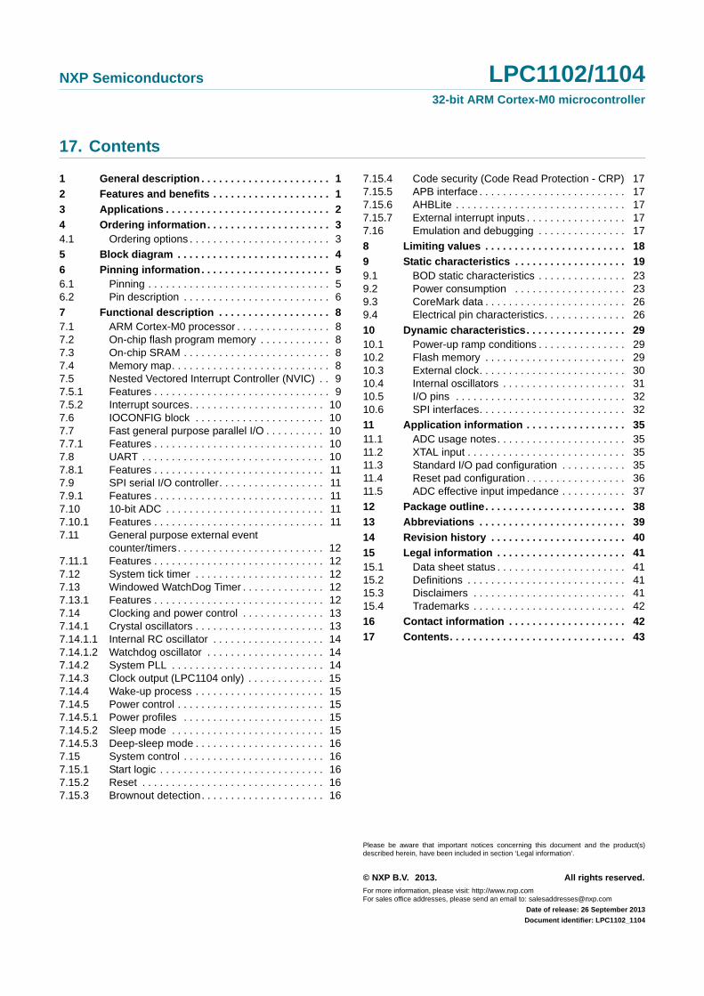
17. Contents
1 General description . . . . . . . . . . . . . . . . . . . . . . 1
2 Features and benefits . . . . . . . . . . . . . . . . . . . . 1
3 Applications . . . . . . . . . . . . . . . . . . . . . . . . . . . . 2
4 Ordering information. . . . . . . . . . . . . . . . . . . . . 34.1 Ordering options . . . . . . . . . . . . . . . . . . . . . . . . 3
5 Block diagram . . . . . . . . . . . . . . . . . . . . . . . . . . 4
6 Pinning information. . . . . . . . . . . . . . . . . . . . . . 56.1 Pinning . . . . . . . . . . . . . . . . . . . . . . . . . . . . . . . 56.2 Pin description . . . . . . . . . . . . . . . . . . . . . . . . . 6
7 Functional description . . . . . . . . . . . . . . . . . . . 87.1 ARM Cortex-M0 processor . . . . . . . . . . . . . . . . 87.2 On-chip flash program memory . . . . . . . . . . . . 87.3 On-chip SRAM . . . . . . . . . . . . . . . . . . . . . . . . . 87.4 Memory map. . . . . . . . . . . . . . . . . . . . . . . . . . . 87.5 Nested Vectored Interrupt Controller (NVIC) . . 97.5.1 Features . . . . . . . . . . . . . . . . . . . . . . . . . . . . . . 97.5.2 Interrupt sources. . . . . . . . . . . . . . . . . . . . . . . 107.6 IOCONFIG block . . . . . . . . . . . . . . . . . . . . . . 107.7 Fast general purpose parallel I/O . . . . . . . . . . 107.7.1 Features . . . . . . . . . . . . . . . . . . . . . . . . . . . . . 107.8 UART . . . . . . . . . . . . . . . . . . . . . . . . . . . . . . . 107.8.1 Features . . . . . . . . . . . . . . . . . . . . . . . . . . . . . 117.9 SPI serial I/O controller. . . . . . . . . . . . . . . . . . 117.9.1 Features . . . . . . . . . . . . . . . . . . . . . . . . . . . . . 117.10 10-bit ADC . . . . . . . . . . . . . . . . . . . . . . . . . . . 117.10.1 Features . . . . . . . . . . . . . . . . . . . . . . . . . . . . . 117.11 General purpose external event
counter/timers. . . . . . . . . . . . . . . . . . . . . . . . . 127.11.1 Features . . . . . . . . . . . . . . . . . . . . . . . . . . . . . 127.12 System tick timer . . . . . . . . . . . . . . . . . . . . . . 127.13 Windowed WatchDog Timer . . . . . . . . . . . . . . 127.13.1 Features . . . . . . . . . . . . . . . . . . . . . . . . . . . . . 127.14 Clocking and power control . . . . . . . . . . . . . . 137.14.1 Crystal oscillators . . . . . . . . . . . . . . . . . . . . . . 137.14.1.1 Internal RC oscillator . . . . . . . . . . . . . . . . . . . 147.14.1.2 Watchdog oscillator . . . . . . . . . . . . . . . . . . . . 147.14.2 System PLL . . . . . . . . . . . . . . . . . . . . . . . . . . 147.14.3 Clock output (LPC1104 only) . . . . . . . . . . . . . 157.14.4 Wake-up process . . . . . . . . . . . . . . . . . . . . . . 157.14.5 Power control . . . . . . . . . . . . . . . . . . . . . . . . . 157.14.5.1 Power profiles . . . . . . . . . . . . . . . . . . . . . . . . 157.14.5.2 Sleep mode . . . . . . . . . . . . . . . . . . . . . . . . . . 157.14.5.3 Deep-sleep mode . . . . . . . . . . . . . . . . . . . . . . 167.15 System control . . . . . . . . . . . . . . . . . . . . . . . . 167.15.1 Start logic . . . . . . . . . . . . . . . . . . . . . . . . . . . . 167.15.2 Reset . . . . . . . . . . . . . . . . . . . . . . . . . . . . . . . 167.15.3 Brownout detection. . . . . . . . . . . . . . . . . . . . . 16
7.15.4 Code security (Code Read Protection - CRP) 177.15.5 APB interface . . . . . . . . . . . . . . . . . . . . . . . . . 177.15.6 AHBLite . . . . . . . . . . . . . . . . . . . . . . . . . . . . . 177.15.7 External interrupt inputs . . . . . . . . . . . . . . . . . 177.16 Emulation and debugging . . . . . . . . . . . . . . . 17
8 Limiting values . . . . . . . . . . . . . . . . . . . . . . . . 18
9 Static characteristics . . . . . . . . . . . . . . . . . . . 199.1 BOD static characteristics . . . . . . . . . . . . . . . 239.2 Power consumption . . . . . . . . . . . . . . . . . . . 239.3 CoreMark data . . . . . . . . . . . . . . . . . . . . . . . . 269.4 Electrical pin characteristics. . . . . . . . . . . . . . 26
10 Dynamic characteristics. . . . . . . . . . . . . . . . . 2910.1 Power-up ramp conditions . . . . . . . . . . . . . . . 2910.2 Flash memory . . . . . . . . . . . . . . . . . . . . . . . . 2910.3 External clock. . . . . . . . . . . . . . . . . . . . . . . . . 3010.4 Internal oscillators . . . . . . . . . . . . . . . . . . . . . 3110.5 I/O pins . . . . . . . . . . . . . . . . . . . . . . . . . . . . . 3210.6 SPI interfaces. . . . . . . . . . . . . . . . . . . . . . . . . 32
11 Application information . . . . . . . . . . . . . . . . . 3511.1 ADC usage notes. . . . . . . . . . . . . . . . . . . . . . 3511.2 XTAL input . . . . . . . . . . . . . . . . . . . . . . . . . . . 3511.3 Standard I/O pad configuration . . . . . . . . . . . 3511.4 Reset pad configuration . . . . . . . . . . . . . . . . . 3611.5 ADC effective input impedance . . . . . . . . . . . 37
12 Package outline. . . . . . . . . . . . . . . . . . . . . . . . 38
13 Abbreviations . . . . . . . . . . . . . . . . . . . . . . . . . 39
14 Revision history . . . . . . . . . . . . . . . . . . . . . . . 40
15 Legal information . . . . . . . . . . . . . . . . . . . . . . 4115.1 Data sheet status . . . . . . . . . . . . . . . . . . . . . . 4115.2 Definitions . . . . . . . . . . . . . . . . . . . . . . . . . . . 4115.3 Disclaimers . . . . . . . . . . . . . . . . . . . . . . . . . . 4115.4 Trademarks . . . . . . . . . . . . . . . . . . . . . . . . . . 42
16 Contact information . . . . . . . . . . . . . . . . . . . . 42
17 Contents. . . . . . . . . . . . . . . . . . . . . . . . . . . . . . 43
© NXP B.V. 2013. All rights reserved.
For more information, please visit: http://www.nxp.comFor sales office addresses, please send an email to: [email protected]
Date of release: 26 September 2013
Document identifier: LPC1102_1104
Please be aware that important notices concerning this document and the product(s)described herein, have been included in section ‘Legal information’.


![LPC1102/1104 32-bit ARM Cortex-M0 …When configured as a ADC input, digital section of the pad is disabled and the pin is not 5 V tolerant (see Figure 21). [5] When the external clock](https://img.pdfslide.net/doc/110x75/5e70cc1d5875163bd0796788/lpc11021104-32-bit-arm-cortex-m0-when-configured-as-a-adc-input-digital-section.jpg)