Embed Size (px)
Citation preview
1. General description
The LPC12D27 are ARM Cortex-M0 based microcontrollers for embedded applications featuring a high level of integration and low power consumption. The ARM Cortex-M0 is a next generation core that offers system enhancements such as enhanced debug features and a higher level of support block integration.
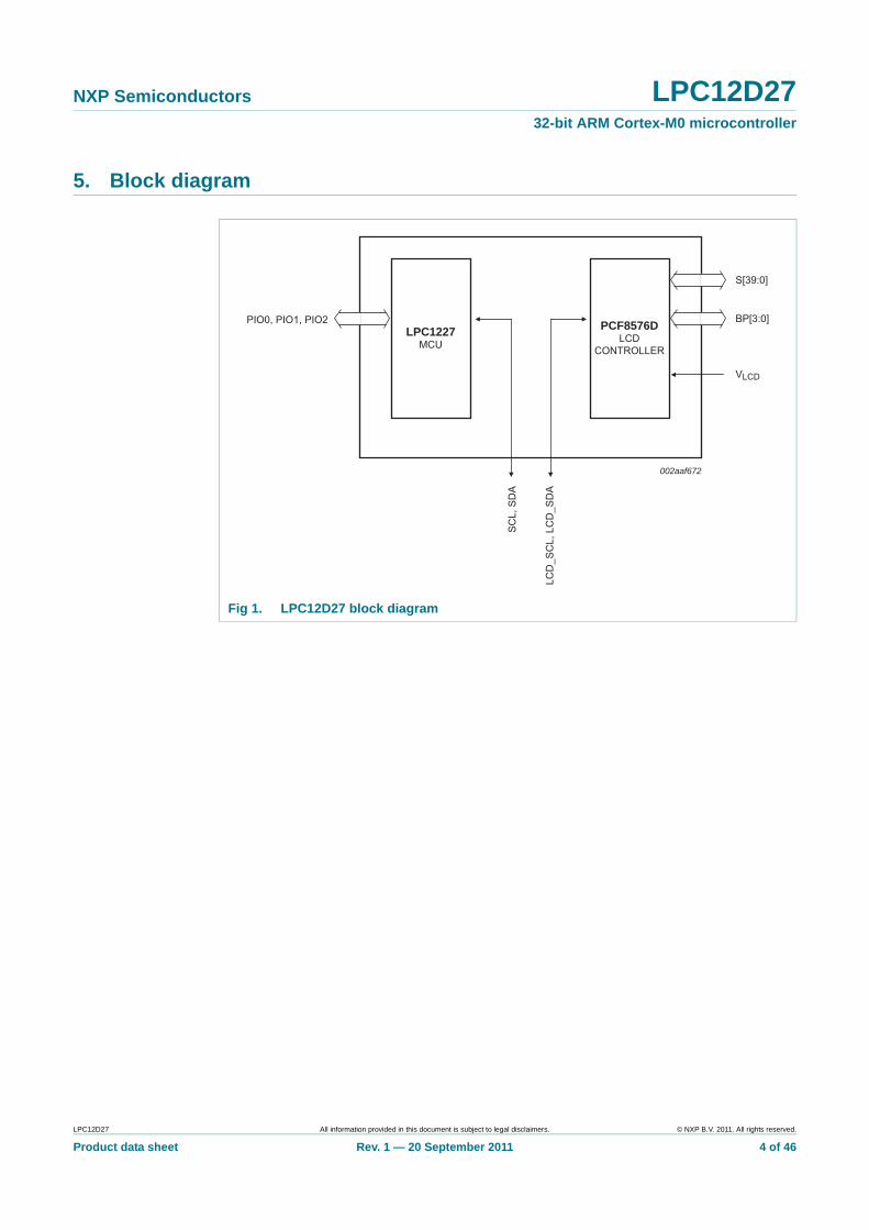
The LPC12D27 is a dual-chip module consisting of a LPC1227 single-chip microcontroller combined with a PCF8576D Universal LCD driver in a low-cost 100-pin package. The LCD driver provides 40 segments and supports from one to four backplanes. Display overhead is minimized by an on-chip display RAM with auto-increment addressing.
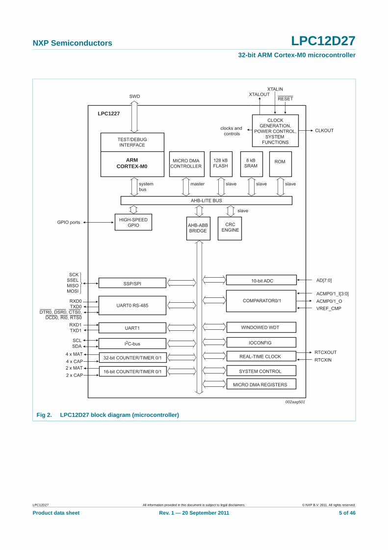
The LPC12D27 operate at CPU frequencies of up to 45 MHz and include 128 kB of flash memory and 8 kB of data memory.
The peripheral complement of the LPC1227 microcontroller includes a micro DMA controller, one Fast-mode Plus I2C interface, one SSP interface, two UARTs, four general purpose timers, a 10-bit ADC, two comparators, and up to 40 general purpose I/O pins.
Remark: For a functional description of the LPC1227 microcontroller see the LPC122x data sheet. For a detailed description of the LCD driver see the PCF8576D data sheet. Both data sheets are available at http://www.nxp.com/microcontrollers
2. Features and benefits
LCD driver
40 segments.
One to four backplanes.
On-chip display RAM with auto-increment addressing.
Processor core
ARM Cortex-M0 processor, running at frequencies of up to 45 MHz (one wait state from flash) or 30 MHz (zero wait states from flash). The LPC12D27 have a high score of over 45 in CoreMark CPU performance benchmark testing, equivalent to 1.51/MHz.
ARM Cortex-M0 built-in Nested Vectored Interrupt Controller (NVIC).
Serial Wire Debug (SWD).
System tick timer.
Memory
8 kB SRAM.
128 kB on-chip flash programming memory.
LPC12D2732-bit ARM Cortex-M0 microcontroller; 128 kB flash and 8 kB SRAM; 40 segment x 4 LCD driver Rev. 1 — 20 September 2011 Product data sheet
NXP Semiconductors LPC12D2732-bit ARM Cortex-M0 microcontroller
In-System Programming (ISP) and In-Application Programming (IAP) via on-chip bootloader software.
Includes ROM-based 32-bit integer division routines.
Clock generation unit
Crystal oscillator with an operating range of 1 MHz to 25 MHz.
12 MHz Internal RC (IRC) oscillator trimmed to 1 % accuracy that can optionally be used as a system clock.
PLL allows CPU operation up to the maximum CPU rate without the need for a high-frequency crystal. May be run from the system oscillator or the internal RC oscillator.
Clock output function with divider that can reflect the system oscillator clock, IRC clock, main clock, and Watchdog clock.
Real-Time Clock (RTC).
Digital peripherals
Micro DMA controller with 21 channels.
CRC engine.
Two UARTs with fractional baud rate generation and internal FIFO. One UART with RS-485 and modem support and one standard UART with IrDA.
SSP/SPI controller with FIFO and multi-protocol capabilities.
I2C-bus interface supporting full I2C-bus specification and Fast-mode Plus with a data rate of 1 Mbit/s with multiple address recognition and monitor mode. I2C-bus pins have programmable glitch filter.
Up to 40 General Purpose I/O (GPIO) pins with programmable pull-up resistor, open-drain mode, programmable digital input glitch filter, and programmable input inverter.
Programmable output drive on all GPIO pins. Four pins support high-current output drivers.
All GPIO pins can be used as edge and level sensitive interrupt sources.
Four general purpose counter/timers with four capture inputs and four match outputs (32-bit timers) or two capture inputs and two match outputs (16-bit timers).
Windowed WatchDog Timer (WWDT), IEC-60335 Class B certified.
Analog peripherals
One 8-channel, 10-bit ADC.
Two highly flexible analog comparators. Comparator outputs can be programmed to trigger a timer match signal or can be used to emulate 555 timer behavior.
Power
Three reduced power modes: Sleep, Deep-sleep, and Deep power-down.
Processor wake-up from Deep-sleep mode via start logic using 12 port pins.
Processor wake-up from Deep-power down and Deep-sleep modes via the RTC.
Brownout detect with three separate thresholds each for interrupt and forced reset.
Power-On Reset (POR).
Integrated PMU (Power Management Unit).
Unique device serial number for identification.
3.3 V power supply.
Available as 100-pin LQFP package.
LPC12D27 All information provided in this document is subject to legal disclaimers. © NXP B.V. 2011. All rights reserved.
Product data sheet Rev. 1 — 20 September 2011 2 of 46
NXP Semiconductors LPC12D2732-bit ARM Cortex-M0 microcontroller
3. Applications
White goods
Portable medical devices
Lighting control
Thermostats
Alarm systems
4. Ordering information
4.1 Ordering options
Table 1. Ordering information
Type number Package
Name Description Version
LPC12D27FBD100/301 LQFP100 plastic low profile quad flat package; 100 leads; body 14 14 1.4 mm SOT407-1
Table 2. Ordering options for LPC12D27
Type number Flash Total SRAM UART RS-485
I2C/ FM+ SSP ADC channels
Package
LPC12D27FBD100/301 128 kB 8 kB 1 1 1 8 LQFP100
LPC12D27 All information provided in this document is subject to legal disclaimers. © NXP B.V. 2011. All rights reserved.
Product data sheet Rev. 1 — 20 September 2011 3 of 46
NXP Semiconductors LPC12D2732-bit ARM Cortex-M0 microcontroller
5. Block diagram
Fig 1. LPC12D27 block diagram
SC
L, S
DA
LCD
_SC
L, L
CD
_SD
A
VLCD
LPC1227MCU
PCF8576DLCD
CONTROLLER
PIO0, PIO1, PIO2
S[39:0]
BP[3:0]
002aaf672
LPC12D27 All information provided in this document is subject to legal disclaimers. © NXP B.V. 2011. All rights reserved.
Product data sheet Rev. 1 — 20 September 2011 4 of 46
NXP Semiconductors LPC12D2732-bit ARM Cortex-M0 microcontroller
Fig 2. LPC12D27 block diagram (microcontroller)
ARMCORTEX-M0
TEST/DEBUGINTERFACE
MICRO DMACONTROLLER
systembus
CLOCKGENERATION,
POWER CONTROL,SYSTEM
FUNCTIONS
XTALINXTALOUT
RESET
clocks and controls
SWD
CRCENGINE
LPC1227
master
128 kBFLASH
slave
8 kBSRAM
slave
ROM
slave
slave
002aag501
GPIO ports
WINDOWED WDT
IOCONFIG
REAL-TIME CLOCK
SYSTEM CONTROL
CLKOUT
SSP/SPI
UART0 RS-485
I2C-bus
32-bit COUNTER/TIMER 0/1
SCKSSELMISOMOSI
4 x MAT4 x CAP
SDASCL
UART1TXD1RXD1
16-bit COUNTER/TIMER 0/12 x MAT2 x CAP
RXD0TXD0
DTR0, DSR0, CTS0,DCD0, RI0, RTS0
10-bit ADC
MICRO DMA REGISTERS
COMPARATOR0/1
AD[7:0]
ACMP0/1_I[3:0]ACMP0/1_OVREF_CMP
AHB-LITE BUS
AHB-ABBBRIDGE
HIGH-SPEEDGPIO
RTCXOUTRTCXIN
LPC12D27 All information provided in this document is subject to legal disclaimers. © NXP B.V. 2011. All rights reserved.
Product data sheet Rev. 1 — 20 September 2011 5 of 46
NXP Semiconductors LPC12D2732-bit ARM Cortex-M0 microcontroller
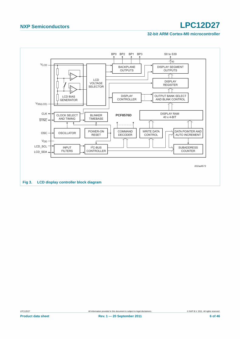
Fig 3. LCD display controller block diagram
40
002aaf673
LCD BIASGENERATOR
LCDVOLTAGE
SELECTOR
PCF8576D
BACKPLANEOUTPUTS
DISPLAYCONTROLLER
COMMANDDECODER
WRITE DATACONTROL
DISPLAY RAM40 x 4-BIT
OUTPUT BANK SELECTAND BLINK CONTROL
DISPLAYREGISTER
DISPLAY SEGMENTOUTPUTS
DATA POINTER ANDAUTO INCREMENT
SUBADDRESSCOUNTER
CLOCK SELECTAND TIMING
OSCILLATOR
INPUTFILTERS
BLINKERTIMEBASE
POWER-ONRESET
I2C-BUSCONTROLLER
BP0 BP2 BP1 BP3
VDD
OSC
SYNC
S0 to S39
LCD_SDA
LCD_SCL
CLK
VSS(LCD)
VLCD
LPC12D27 All information provided in this document is subject to legal disclaimers. © NXP B.V. 2011. All rights reserved.
Product data sheet Rev. 1 — 20 September 2011 6 of 46
NXP Semiconductors LPC12D2732-bit ARM Cortex-M0 microcontroller
6. Pinning information
6.1 Pinning
Fig 4. Pin configuration LQFP100 package
LPC12D27
SWDIO/PIO0_25 S29
SWCLK/PIO0_26 S28
PIO0_27 S27
PIO0_28 S26
PIO0_29 S25
PIO0_0 S24
PIO0_1 S23
PIO0_2 S22
PIO0_3 S21
PIO0_4 S20
PIO0_5 S19
PIO0_6 S18
PIO0_7 S17
PIO0_8 S16
RESET/PIO0_13 S10
PIO0_14 S9
PIO0_15 S8
PIO0_16 S7
PIO0_17
PIO0_9
PIO2_0
PIO0_10
PIO0_11
PIO0_12
S6
S15
S14
S13
S12
S11
PIO0_18 S5
R/P
IO0_
30P
IO0_
24
R/P
IO0_
31P
IO0_
23
R/P
IO1_
0P
IO0_
22
S34
PIO
0_21
S35
PIO
0_20
S36
PIO
0_19
S37
VR
EF_
CM
P
S38
XTA
LOU
T
S39
XTA
LIN
LCD
_ S
DA
VS
SIO
LCD
_ S
CL
VD
D(IO
)
SY
NC
RTC
XIN
CLK
RTC
XO
UT
VD
DV
DD
(3V
3)
BP
3P
IO1_
2
S0
R/P
IO1_
1
S1
S33
S2
S32
S3
VS
S(L
CD
)
VLC
D
BP
0
BP
2
BP
1
S31
VS
S
PIO
1_6
PIO
1_5
PIO
1_4
PIO
1_3
S4
S30
002aag502
1
2
3
4
5
6
7
8
9
10
11
12
13
14
20
21
22
23
24
25
75
74
73
72
71
70
69
68
67
66
65
64
63
62
56
55
54
53
52
51
15
16
17
18
19
61
60
59
58
57
26 27 28 29 30 31 32 33 34 35 36 37 38 39 45 46 47 48 49 50
100
99 98 97 96 95 94 93 92 91 90 89 88 87 81 80 79 78 77 76
40 41 42 43 44
86 85 84 83 82
LPC12D27 All information provided in this document is subject to legal disclaimers. © NXP B.V. 2011. All rights reserved.
Product data sheet Rev. 1 — 20 September 2011 7 of 46
NXP Semiconductors LPC12D2732-bit ARM Cortex-M0 microcontroller
6.2 Pin description
All pins except the supply pins and the LCD pins can have more than one function as shown in Table 3. The pin function is selected through the pin’s IOCON register in the IOCONFIG block. The multiplexed functions include the counter/timer inputs and outputs, the UART receive, transmit, and control functions, and the serial wire debug functions.
For each pin, the default function is listed first together with the pin’s reset state.
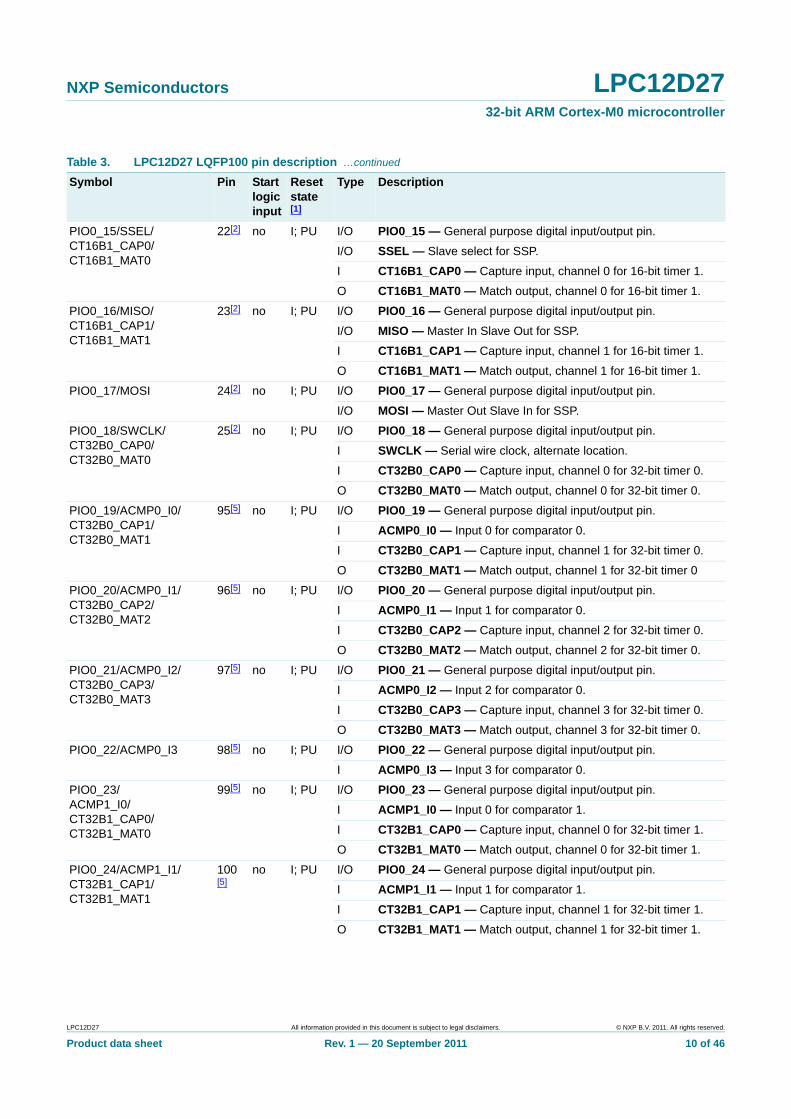
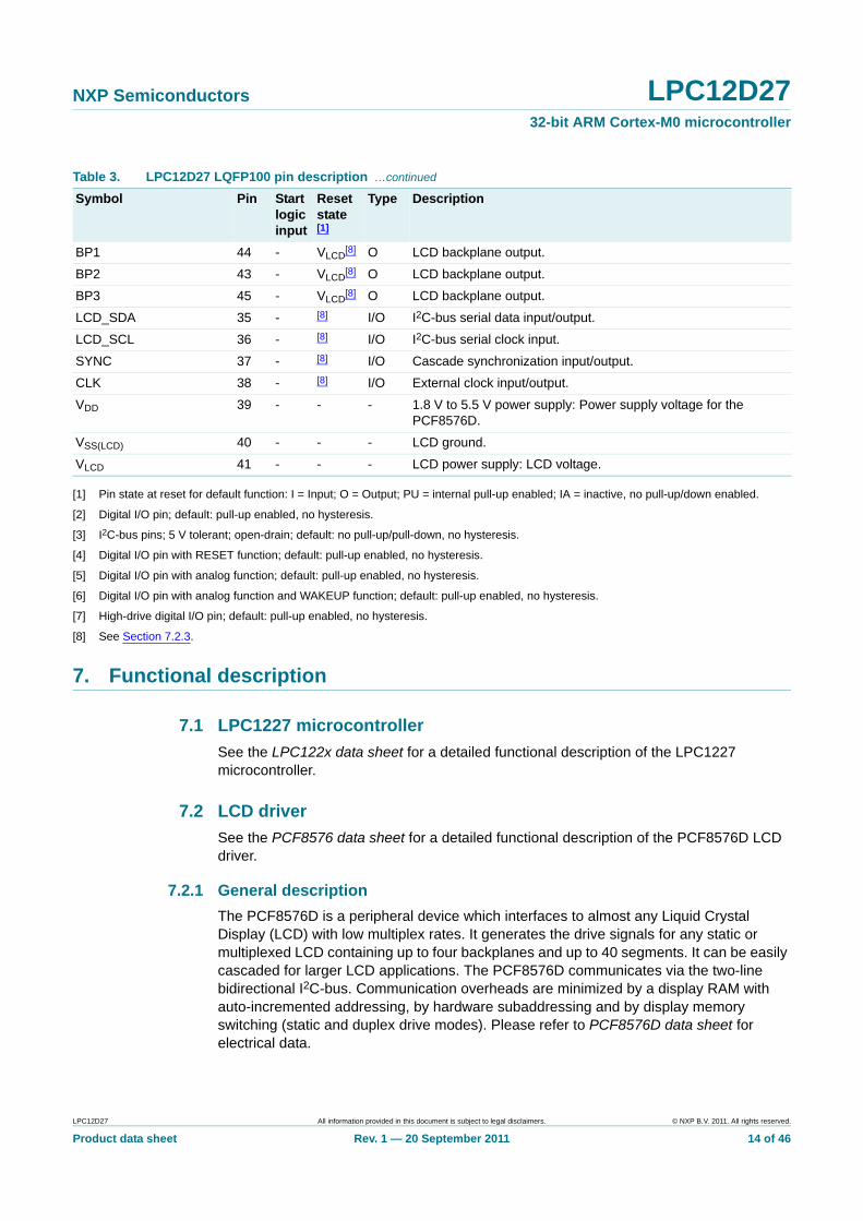
Table 3. LPC12D27 LQFP100 pin description
Symbol Pin Start logic input
Reset state[1]
Type Description
Microcontroller pins
PIO0_0 to PIO0_31 I/O Port 0 — Port 0 is a 32-bit I/O port with individual direction and function controls for each bit. The operation of port 0 pins depends on the function selected through the IOCONFIG register block.
PIO0_0/RTS0 6[2] yes I; PU I/O PIO0_0 — General purpose digital input/output pin. Also serves as wake-up pin from Deep-sleep mode.
O RTS0 — Request To Send output for UART0.
PIO0_1/RXD0/CT32B0_CAP0/CT32B0_MAT0
7[2] yes I; PU I/O PIO0_1 — General purpose digital input/output pin. Also serves as wake-up pin from Deep-sleep mode.
I RXD0 — Receiver input for UART0.
I CT32B0_CAP0 — Capture input, channel 0 for 32-bit timer 0.
O CT32B0_MAT0 — Match output, channel 0 for 32-bit timer 0.
PIO0_2/TXD0/CT32B0_CAP1/CT32B0_MAT1
8[2] yes I; PU I/O PIO0_2 — General purpose digital input/output pin. Also serves as wake-up pin from Deep-sleep mode.
O TXD0 — Transmitter output for UART0.
I CT32B0_CAP1 — Capture input, channel 1 for 32-bit timer 0.
O CT32B0_MAT1 — Match output, channel 1 for 32-bit timer 0.
PIO0_3/DTR0/CT32B0_CAP2/CT32B0_MAT2
9[2] yes I; PU I/O PIO0_3 — General purpose digital input/output pin. Also serves as wake-up pin from Deep-sleep mode.
O DTR0 — Data Terminal Ready output for UART0.
I CT32B0_CAP2 — Capture input, channel 2 for 32-bit timer 0.
O CT32B0_MAT2 — Match output, channel 2 for 32-bit timer 0.
PIO0_4/CT32B0_CAP3/CT32B0_MAT3
10[2] yes I; PU I/O PIO0_4 — General purpose digital input/output pin. Also serves as wake-up pin from Deep-sleep mode.
I DSR0 — Data Set Ready input for UART0.
I CT32B0_CAP3 — Capture input, channel 3 for 32-bit timer 0.
O CT32B0_MAT3 — Match output, channel 3 for 32-bit timer 0.
PIO0_5/DCD0 11[2] yes I; PU I/O PIO0_5 — General purpose digital input/output pin. Also serves as wake-up pin from Deep-sleep mode.
I DCD0 — Data Carrier Detect input for UART0.
LPC12D27 All information provided in this document is subject to legal disclaimers. © NXP B.V. 2011. All rights reserved.
Product data sheet Rev. 1 — 20 September 2011 8 of 46
NXP Semiconductors LPC12D2732-bit ARM Cortex-M0 microcontroller
PIO0_6/RI0/CT32B1_CAP0/CT32B1_MAT0
12[2] yes I; PU I/O PIO0_6 — General purpose digital input/output pin. Also serves as wake-up pin from Deep-sleep mode.
I RI0 — Ring Indicator input for UART0.
I CT32B1_CAP0 — Capture input, channel 0 for 32-bit timer 1.
O CT32B1_MAT0 — Match output, channel 0 for 32-bit timer 1.
PIO0_7/CTS0/CT32B1_CAP1/CT32B1_MAT1
13[2] yes I; PU I/O PIO0_7 — General purpose digital input/output pin. Also serves as wake-up pin from Deep-sleep mode.
I CTS0 — Clear To Send input for UART0.
I CT32B1_CAP1 — Capture input, channel 1 for 32-bit timer 1.
O CT32B1_MAT1 — Match output, channel 1 for 32-bit timer 1.
PIO0_8/RXD1/CT32B1_CAP2/CT32B1_MAT2
14[2] yes I; PU I/O PIO0_8 — General purpose digital input/output pin. Also serves as wake-up pin from Deep-sleep mode.
I RXD1 — Receiver input for UART1.
I CT32B1_CAP2 — Capture input, channel 2 for 32-bit timer 1.
O CT32B1_MAT2 — Match output, channel 2 for 32-bit timer 1.
PIO0_9/TXD1/CT32B1_CAP3/CT32B1_MAT3
15[2] yes I; PU I/O PIO0_9 — General purpose digital input/output pin. Also serves as wake-up pin from Deep-sleep mode.
O TXD1 — Transmitter output for UART1.
I CT32B1_CAP3 — Capture input, channel 3 for 32-bit timer 1.
O CT32B1_MAT3 — Match output, channel 3 for 32-bit timer 1.
PIO0_10/SCL 17[3] yes I; IA I/O PIO0_10 — General purpose digital input/output pin. Also serves as wake-up pin from Deep-sleep mode.
I/O SCL — I2C-bus clock input/output.
PIO0_11/SDA/CT16B0_CAP0/CT16B0_MAT0
18[3] yes I; IA I/O PIO0_11 — General purpose digital input/output pin. Also serves as wake-up pin from Deep-sleep mode.
I/O SDA — I2C-bus data input/output.
I CT16B0_CAP0 — Capture input, channel 0 for 16-bit timer 0.
O CT16B0_MAT0 — Match output, channel 0 for 16-bit timer 0.
PIO0_12/CLKOUT/CT16B0_CAP1/CT16B0_MAT1
19[7] no I; PU I/O PIO0_12 — General purpose digital input/output pin. A LOW level on this pin in during reset starts the ISP command handler. High-current output driver.
O CLKOUT — Clock out pin.
I CT16B0_CAP1 — Capture input, channel 0 for 16-bit timer 0.
O CT16B0_MAT1 — Match output, channel 1 for 16-bit timer 0.
RESET/PIO0_13 20[4] no I; PU I RESET — External reset input: A LOW on this pin resets the device, causing I/O ports and peripherals to take on their default states, and processor execution to begin at address 0.
I/O PIO0_13 — General purpose digital input/output pin.
PIO0_14/SCK 21[2] no I; PU I/O PIO0_14 — General purpose digital input/output pin.
I/O SCK — Serial clock for SSP.
Table 3. LPC12D27 LQFP100 pin description …continued
Symbol Pin Start logic input
Reset state[1]
Type Description
LPC12D27 All information provided in this document is subject to legal disclaimers. © NXP B.V. 2011. All rights reserved.
Product data sheet Rev. 1 — 20 September 2011 9 of 46
NXP Semiconductors LPC12D2732-bit ARM Cortex-M0 microcontroller
PIO0_15/SSEL/CT16B1_CAP0/CT16B1_MAT0
22[2] no I; PU I/O PIO0_15 — General purpose digital input/output pin.
I/O SSEL — Slave select for SSP.
I CT16B1_CAP0 — Capture input, channel 0 for 16-bit timer 1.
O CT16B1_MAT0 — Match output, channel 0 for 16-bit timer 1.
PIO0_16/MISO/CT16B1_CAP1/CT16B1_MAT1
23[2] no I; PU I/O PIO0_16 — General purpose digital input/output pin.
I/O MISO — Master In Slave Out for SSP.
I CT16B1_CAP1 — Capture input, channel 1 for 16-bit timer 1.
O CT16B1_MAT1 — Match output, channel 1 for 16-bit timer 1.
PIO0_17/MOSI 24[2] no I; PU I/O PIO0_17 — General purpose digital input/output pin.
I/O MOSI — Master Out Slave In for SSP.
PIO0_18/SWCLK/CT32B0_CAP0/CT32B0_MAT0
25[2] no I; PU I/O PIO0_18 — General purpose digital input/output pin.
I SWCLK — Serial wire clock, alternate location.
I CT32B0_CAP0 — Capture input, channel 0 for 32-bit timer 0.
O CT32B0_MAT0 — Match output, channel 0 for 32-bit timer 0.
PIO0_19/ACMP0_I0/CT32B0_CAP1/CT32B0_MAT1
95[5] no I; PU I/O PIO0_19 — General purpose digital input/output pin.
I ACMP0_I0 — Input 0 for comparator 0.
I CT32B0_CAP1 — Capture input, channel 1 for 32-bit timer 0.
O CT32B0_MAT1 — Match output, channel 1 for 32-bit timer 0
PIO0_20/ACMP0_I1/CT32B0_CAP2/CT32B0_MAT2
96[5] no I; PU I/O PIO0_20 — General purpose digital input/output pin.
I ACMP0_I1 — Input 1 for comparator 0.
I CT32B0_CAP2 — Capture input, channel 2 for 32-bit timer 0.
O CT32B0_MAT2 — Match output, channel 2 for 32-bit timer 0.
PIO0_21/ACMP0_I2/CT32B0_CAP3/CT32B0_MAT3
97[5] no I; PU I/O PIO0_21 — General purpose digital input/output pin.
I ACMP0_I2 — Input 2 for comparator 0.
I CT32B0_CAP3 — Capture input, channel 3 for 32-bit timer 0.
O CT32B0_MAT3 — Match output, channel 3 for 32-bit timer 0.
PIO0_22/ACMP0_I3 98[5] no I; PU I/O PIO0_22 — General purpose digital input/output pin.
I ACMP0_I3 — Input 3 for comparator 0.
PIO0_23/ACMP1_I0/CT32B1_CAP0/CT32B1_MAT0
99[5] no I; PU I/O PIO0_23 — General purpose digital input/output pin.
I ACMP1_I0 — Input 0 for comparator 1.
I CT32B1_CAP0 — Capture input, channel 0 for 32-bit timer 1.
O CT32B1_MAT0 — Match output, channel 0 for 32-bit timer 1.
PIO0_24/ACMP1_I1/CT32B1_CAP1/CT32B1_MAT1
100[5]
no I; PU I/O PIO0_24 — General purpose digital input/output pin.
I ACMP1_I1 — Input 1 for comparator 1.
I CT32B1_CAP1 — Capture input, channel 1 for 32-bit timer 1.
O CT32B1_MAT1 — Match output, channel 1 for 32-bit timer 1.
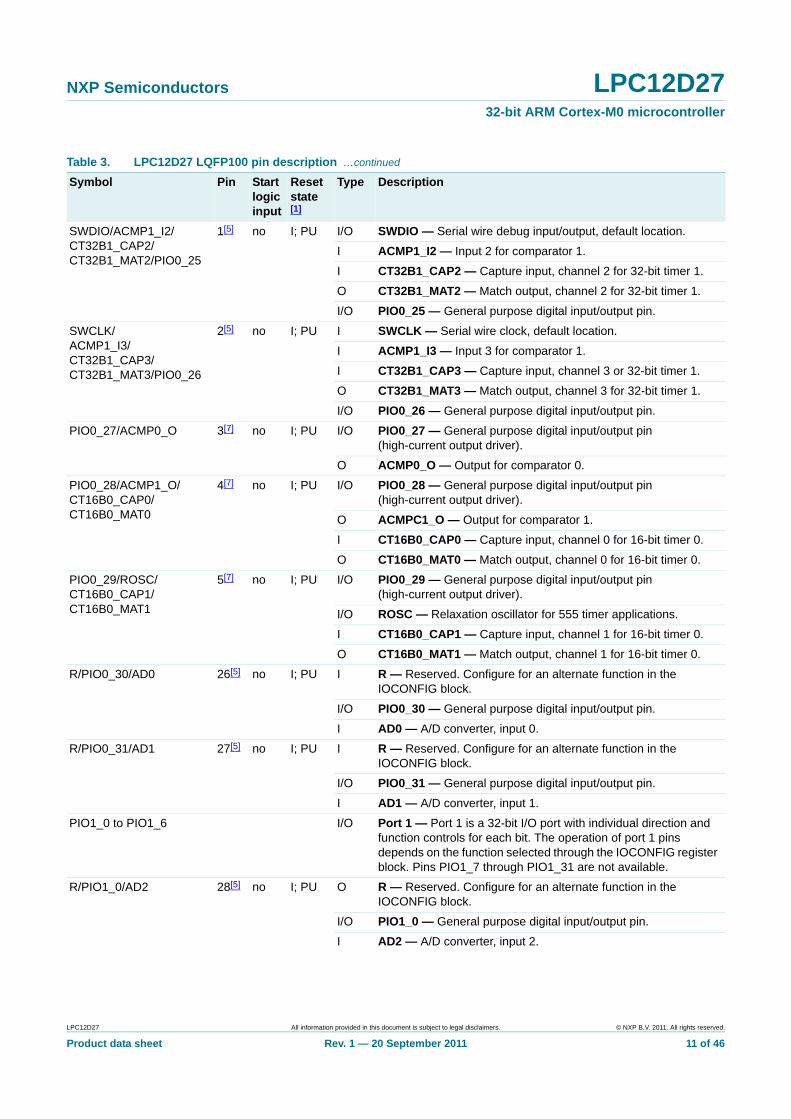
Table 3. LPC12D27 LQFP100 pin description …continued
Symbol Pin Start logic input
Reset state[1]
Type Description
LPC12D27 All information provided in this document is subject to legal disclaimers. © NXP B.V. 2011. All rights reserved.
Product data sheet Rev. 1 — 20 September 2011 10 of 46
NXP Semiconductors LPC12D2732-bit ARM Cortex-M0 microcontroller
SWDIO/ACMP1_I2/CT32B1_CAP2/CT32B1_MAT2/PIO0_25
1[5] no I; PU I/O SWDIO — Serial wire debug input/output, default location.
I ACMP1_I2 — Input 2 for comparator 1.
I CT32B1_CAP2 — Capture input, channel 2 for 32-bit timer 1.
O CT32B1_MAT2 — Match output, channel 2 for 32-bit timer 1.
I/O PIO0_25 — General purpose digital input/output pin.
SWCLK/ACMP1_I3/CT32B1_CAP3/CT32B1_MAT3/PIO0_26
2[5] no I; PU I SWCLK — Serial wire clock, default location.
I ACMP1_I3 — Input 3 for comparator 1.
I CT32B1_CAP3 — Capture input, channel 3 or 32-bit timer 1.
O CT32B1_MAT3 — Match output, channel 3 for 32-bit timer 1.
I/O PIO0_26 — General purpose digital input/output pin.
PIO0_27/ACMP0_O 3[7] no I; PU I/O PIO0_27 — General purpose digital input/output pin (high-current output driver).
O ACMP0_O — Output for comparator 0.
PIO0_28/ACMP1_O/CT16B0_CAP0/CT16B0_MAT0
4[7] no I; PU I/O PIO0_28 — General purpose digital input/output pin (high-current output driver).
O ACMPC1_O — Output for comparator 1.
I CT16B0_CAP0 — Capture input, channel 0 for 16-bit timer 0.
O CT16B0_MAT0 — Match output, channel 0 for 16-bit timer 0.
PIO0_29/ROSC/CT16B0_CAP1/CT16B0_MAT1
5[7] no I; PU I/O PIO0_29 — General purpose digital input/output pin (high-current output driver).
I/O ROSC — Relaxation oscillator for 555 timer applications.
I CT16B0_CAP1 — Capture input, channel 1 for 16-bit timer 0.
O CT16B0_MAT1 — Match output, channel 1 for 16-bit timer 0.
R/PIO0_30/AD0 26[5] no I; PU I R — Reserved. Configure for an alternate function in the IOCONFIG block.
I/O PIO0_30 — General purpose digital input/output pin.
I AD0 — A/D converter, input 0.
R/PIO0_31/AD1 27[5] no I; PU I R — Reserved. Configure for an alternate function in the IOCONFIG block.
I/O PIO0_31 — General purpose digital input/output pin.
I AD1 — A/D converter, input 1.
PIO1_0 to PIO1_6 I/O Port 1 — Port 1 is a 32-bit I/O port with individual direction and function controls for each bit. The operation of port 1 pins depends on the function selected through the IOCONFIG register block. Pins PIO1_7 through PIO1_31 are not available.
R/PIO1_0/AD2 28[5] no I; PU O R — Reserved. Configure for an alternate function in the IOCONFIG block.
I/O PIO1_0 — General purpose digital input/output pin.
I AD2 — A/D converter, input 2.
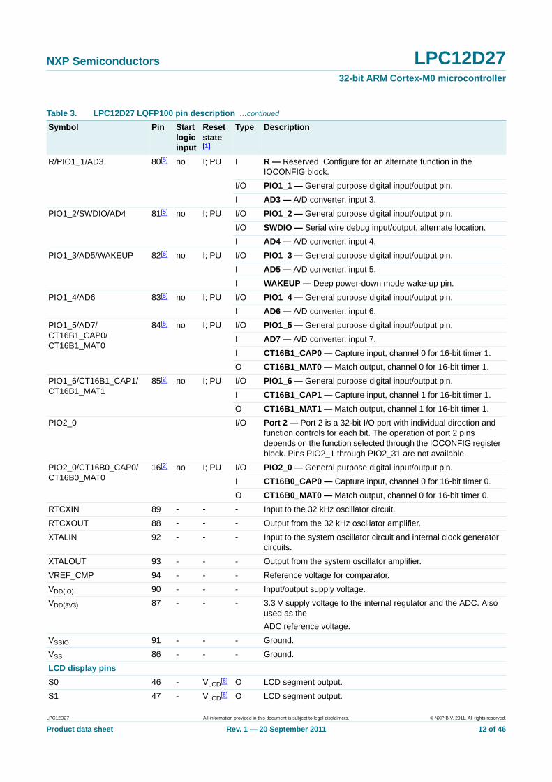
Table 3. LPC12D27 LQFP100 pin description …continued
Symbol Pin Start logic input
Reset state[1]
Type Description
LPC12D27 All information provided in this document is subject to legal disclaimers. © NXP B.V. 2011. All rights reserved.
Product data sheet Rev. 1 — 20 September 2011 11 of 46
NXP Semiconductors LPC12D2732-bit ARM Cortex-M0 microcontroller
R/PIO1_1/AD3 80[5] no I; PU I R — Reserved. Configure for an alternate function in the IOCONFIG block.
I/O PIO1_1 — General purpose digital input/output pin.
I AD3 — A/D converter, input 3.
PIO1_2/SWDIO/AD4 81[5] no I; PU I/O PIO1_2 — General purpose digital input/output pin.
I/O SWDIO — Serial wire debug input/output, alternate location.
I AD4 — A/D converter, input 4.
PIO1_3/AD5/WAKEUP 82[6] no I; PU I/O PIO1_3 — General purpose digital input/output pin.
I AD5 — A/D converter, input 5.
I WAKEUP — Deep power-down mode wake-up pin.
PIO1_4/AD6 83[5] no I; PU I/O PIO1_4 — General purpose digital input/output pin.
I AD6 — A/D converter, input 6.
PIO1_5/AD7/CT16B1_CAP0/CT16B1_MAT0
84[5] no I; PU I/O PIO1_5 — General purpose digital input/output pin.
I AD7 — A/D converter, input 7.
I CT16B1_CAP0 — Capture input, channel 0 for 16-bit timer 1.
O CT16B1_MAT0 — Match output, channel 0 for 16-bit timer 1.
PIO1_6/CT16B1_CAP1/CT16B1_MAT1
85[2] no I; PU I/O PIO1_6 — General purpose digital input/output pin.
I CT16B1_CAP1 — Capture input, channel 1 for 16-bit timer 1.
O CT16B1_MAT1 — Match output, channel 1 for 16-bit timer 1.
PIO2_0 I/O Port 2 — Port 2 is a 32-bit I/O port with individual direction and function controls for each bit. The operation of port 2 pins depends on the function selected through the IOCONFIG register block. Pins PIO2_1 through PIO2_31 are not available.
PIO2_0/CT16B0_CAP0/CT16B0_MAT0
16[2] no I; PU I/O PIO2_0 — General purpose digital input/output pin.
I CT16B0_CAP0 — Capture input, channel 0 for 16-bit timer 0.
O CT16B0_MAT0 — Match output, channel 0 for 16-bit timer 0.
RTCXIN 89 - - - Input to the 32 kHz oscillator circuit.
RTCXOUT 88 - - - Output from the 32 kHz oscillator amplifier.
XTALIN 92 - - - Input to the system oscillator circuit and internal clock generator circuits.
XTALOUT 93 - - - Output from the system oscillator amplifier.
VREF_CMP 94 - - - Reference voltage for comparator.
VDD(IO) 90 - - - Input/output supply voltage.
VDD(3V3) 87 - - - 3.3 V supply voltage to the internal regulator and the ADC. Also used as the
ADC reference voltage.
VSSIO 91 - - - Ground.
VSS 86 - - - Ground.
LCD display pins
S0 46 - VLCD[8] O LCD segment output.
S1 47 - VLCD[8] O LCD segment output.
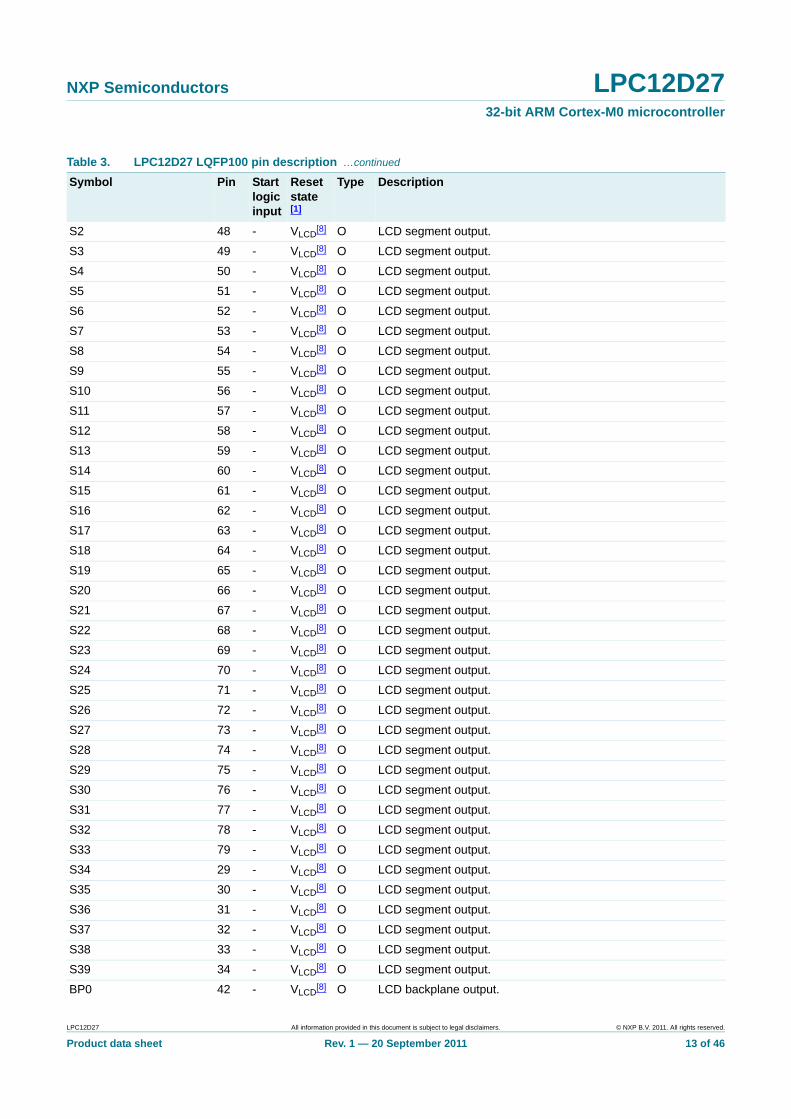
Table 3. LPC12D27 LQFP100 pin description …continued
Symbol Pin Start logic input
Reset state[1]
Type Description
LPC12D27 All information provided in this document is subject to legal disclaimers. © NXP B.V. 2011. All rights reserved.
Product data sheet Rev. 1 — 20 September 2011 12 of 46
NXP Semiconductors LPC12D2732-bit ARM Cortex-M0 microcontroller
S2 48 - VLCD[8] O LCD segment output.
S3 49 - VLCD[8] O LCD segment output.
S4 50 - VLCD[8] O LCD segment output.
S5 51 - VLCD[8] O LCD segment output.
S6 52 - VLCD[8] O LCD segment output.
S7 53 - VLCD[8] O LCD segment output.
S8 54 - VLCD[8] O LCD segment output.
S9 55 - VLCD[8] O LCD segment output.
S10 56 - VLCD[8] O LCD segment output.
S11 57 - VLCD[8] O LCD segment output.
S12 58 - VLCD[8] O LCD segment output.
S13 59 - VLCD[8] O LCD segment output.
S14 60 - VLCD[8] O LCD segment output.
S15 61 - VLCD[8] O LCD segment output.
S16 62 - VLCD[8] O LCD segment output.
S17 63 - VLCD[8] O LCD segment output.
S18 64 - VLCD[8] O LCD segment output.
S19 65 - VLCD[8] O LCD segment output.
S20 66 - VLCD[8] O LCD segment output.
S21 67 - VLCD[8] O LCD segment output.
S22 68 - VLCD[8] O LCD segment output.
S23 69 - VLCD[8] O LCD segment output.
S24 70 - VLCD[8] O LCD segment output.
S25 71 - VLCD[8] O LCD segment output.
S26 72 - VLCD[8] O LCD segment output.
S27 73 - VLCD[8] O LCD segment output.
S28 74 - VLCD[8] O LCD segment output.
S29 75 - VLCD[8] O LCD segment output.
S30 76 - VLCD[8] O LCD segment output.
S31 77 - VLCD[8] O LCD segment output.
S32 78 - VLCD[8] O LCD segment output.
S33 79 - VLCD[8] O LCD segment output.
S34 29 - VLCD[8] O LCD segment output.
S35 30 - VLCD[8] O LCD segment output.
S36 31 - VLCD[8] O LCD segment output.
S37 32 - VLCD[8] O LCD segment output.
S38 33 - VLCD[8] O LCD segment output.
S39 34 - VLCD[8] O LCD segment output.
BP0 42 - VLCD[8] O LCD backplane output.
Table 3. LPC12D27 LQFP100 pin description …continued
Symbol Pin Start logic input
Reset state[1]
Type Description
LPC12D27 All information provided in this document is subject to legal disclaimers. © NXP B.V. 2011. All rights reserved.
Product data sheet Rev. 1 — 20 September 2011 13 of 46
NXP Semiconductors LPC12D2732-bit ARM Cortex-M0 microcontroller
[1] Pin state at reset for default function: I = Input; O = Output; PU = internal pull-up enabled; IA = inactive, no pull-up/down enabled.
[2] Digital I/O pin; default: pull-up enabled, no hysteresis.
[3] I2C-bus pins; 5 V tolerant; open-drain; default: no pull-up/pull-down, no hysteresis.
[4] Digital I/O pin with RESET function; default: pull-up enabled, no hysteresis.
[5] Digital I/O pin with analog function; default: pull-up enabled, no hysteresis.
[6] Digital I/O pin with analog function and WAKEUP function; default: pull-up enabled, no hysteresis.
[7] High-drive digital I/O pin; default: pull-up enabled, no hysteresis.
[8] See Section 7.2.3.
7. Functional description
7.1 LPC1227 microcontroller
See the LPC122x data sheet for a detailed functional description of the LPC1227 microcontroller.
7.2 LCD driver
See the PCF8576 data sheet for a detailed functional description of the PCF8576D LCD driver.
7.2.1 General description
The PCF8576D is a peripheral device which interfaces to almost any Liquid Crystal Display (LCD) with low multiplex rates. It generates the drive signals for any static or multiplexed LCD containing up to four backplanes and up to 40 segments. It can be easily cascaded for larger LCD applications. The PCF8576D communicates via the two-line bidirectional I2C-bus. Communication overheads are minimized by a display RAM with auto-incremented addressing, by hardware subaddressing and by display memory switching (static and duplex drive modes). Please refer to PCF8576D data sheet for electrical data.
BP1 44 - VLCD[8] O LCD backplane output.
BP2 43 - VLCD[8] O LCD backplane output.
BP3 45 - VLCD[8] O LCD backplane output.
LCD_SDA 35 - [8] I/O I2C-bus serial data input/output.
LCD_SCL 36 - [8] I/O I2C-bus serial clock input.
SYNC 37 - [8] I/O Cascade synchronization input/output.
CLK 38 - [8] I/O External clock input/output.
VDD 39 - - - 1.8 V to 5.5 V power supply: Power supply voltage for the PCF8576D.
VSS(LCD) 40 - - - LCD ground.
VLCD 41 - - - LCD power supply: LCD voltage.
Table 3. LPC12D27 LQFP100 pin description …continued
Symbol Pin Start logic input
Reset state[1]
Type Description
LPC12D27 All information provided in this document is subject to legal disclaimers. © NXP B.V. 2011. All rights reserved.
Product data sheet Rev. 1 — 20 September 2011 14 of 46
NXP Semiconductors LPC12D2732-bit ARM Cortex-M0 microcontroller
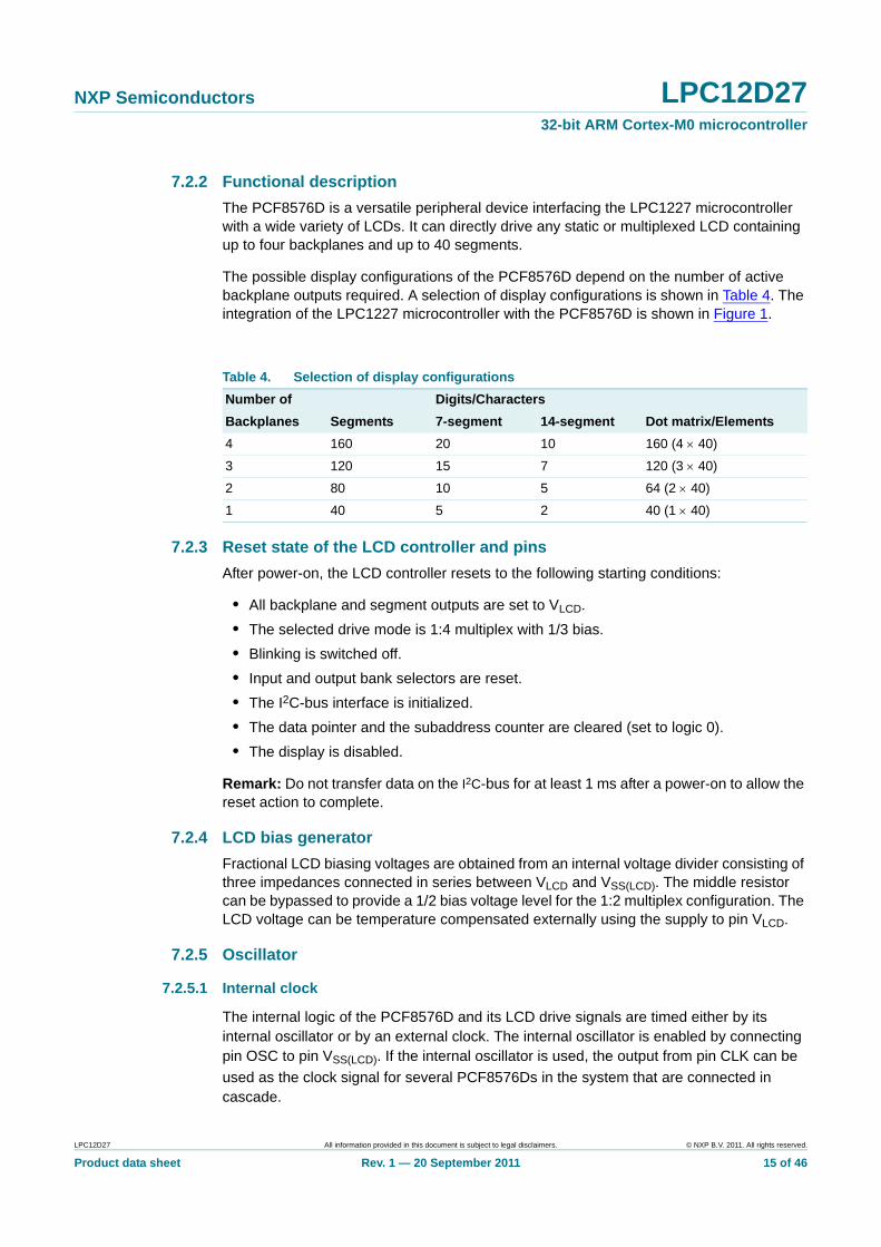
7.2.2 Functional description
The PCF8576D is a versatile peripheral device interfacing the LPC1227 microcontroller with a wide variety of LCDs. It can directly drive any static or multiplexed LCD containing up to four backplanes and up to 40 segments.
The possible display configurations of the PCF8576D depend on the number of active backplane outputs required. A selection of display configurations is shown in Table 4. The integration of the LPC1227 microcontroller with the PCF8576D is shown in Figure 1.
7.2.3 Reset state of the LCD controller and pins
After power-on, the LCD controller resets to the following starting conditions:
• All backplane and segment outputs are set to VLCD.
• The selected drive mode is 1:4 multiplex with 1/3 bias.
• Blinking is switched off.
• Input and output bank selectors are reset.
• The I2C-bus interface is initialized.
• The data pointer and the subaddress counter are cleared (set to logic 0).
• The display is disabled.
Remark: Do not transfer data on the I2C-bus for at least 1 ms after a power-on to allow the reset action to complete.
7.2.4 LCD bias generator
Fractional LCD biasing voltages are obtained from an internal voltage divider consisting of three impedances connected in series between VLCD and VSS(LCD). The middle resistor can be bypassed to provide a 1/2 bias voltage level for the 1:2 multiplex configuration. The LCD voltage can be temperature compensated externally using the supply to pin VLCD.
7.2.5 Oscillator
7.2.5.1 Internal clock
The internal logic of the PCF8576D and its LCD drive signals are timed either by its internal oscillator or by an external clock. The internal oscillator is enabled by connecting pin OSC to pin VSS(LCD). If the internal oscillator is used, the output from pin CLK can be
used as the clock signal for several PCF8576Ds in the system that are connected in cascade.
Table 4. Selection of display configurations
Number of Digits/Characters
Backplanes Segments 7-segment 14-segment Dot matrix/Elements
4 160 20 10 160 (4 40)
3 120 15 7 120 (3 40)
2 80 10 5 64 (2 40)
1 40 5 2 40 (1 40)
LPC12D27 All information provided in this document is subject to legal disclaimers. © NXP B.V. 2011. All rights reserved.
Product data sheet Rev. 1 — 20 September 2011 15 of 46
NXP Semiconductors LPC12D2732-bit ARM Cortex-M0 microcontroller
7.2.6 Timing
The PCF8576D timing controls the internal data flow of the device. This includes the transfer of display data from the display RAM to the display segment outputs. In cascaded applications, the correct timing relationship between each PCF8576D in the system is maintained by the synchronization signal at pin SYNC. The timing also generates the LCD frame signal whose frequency is derived from the clock frequency. The frame signal frequency (ffr) is a fixed division of the clock frequency (fclk) from either the internal or an
external clock: ffr = fclk/24.
7.2.7 Display register
A display latch holds the display data while the corresponding multiplex signals are generated. There is a one-to-one relationship between the data in the display latch, the LCD segment outputs, and each column of the display RAM.
7.2.8 Segment outputs
The LCD drive section includes 40 segment outputs S0 to S39 which should be connected directly to the LCD. The segment output signals are generated in accordance with the multiplexed backplane signals and with data residing in the display latch. When less than 40 segment outputs are required, the unused segment outputs should be left open-circuit.
7.2.9 Backplane outputs
The LCD drive section includes four backplane outputs BP0 to BP3 which must be connected directly to the LCD. The backplane output signals are generated in accordance with the selected LCD drive mode. If less than four backplane outputs are required, the unused outputs can be left open-circuit.
In the 1:3 multiplex drive mode, BP3 carries the same signal as BP1, therefore these two adjacent outputs can be tied together to give enhanced drive capabilities.
In the 1:2 multiplex drive mode, BP0 and BP2, BP1 and BP3 all carry the same signals and may also be paired to increase the drive capabilities.
In the static drive mode the same signal is carried by all four backplane outputs and they can be connected in parallel for very high drive requirements.
7.2.10 Display RAM
The display RAM is a static 40 4-bit RAM which stores LCD data. There is a one-to-one correspondence between the RAM addresses and the segment outputs, and between the individual bits of a RAM word and the backplane outputs. For details, see PCF8576D data sheet.
LPC12D27 All information provided in this document is subject to legal disclaimers. © NXP B.V. 2011. All rights reserved.
Product data sheet Rev. 1 — 20 September 2011 16 of 46
NXP Semiconductors LPC12D2732-bit ARM Cortex-M0 microcontroller
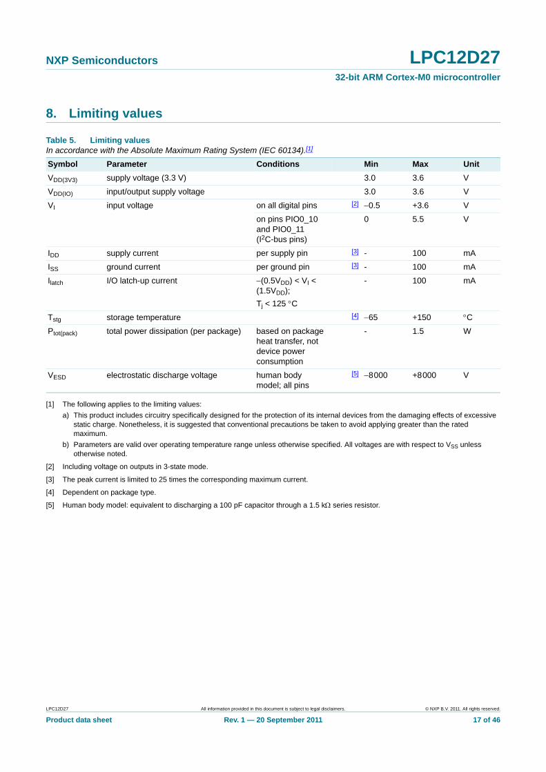
8. Limiting values
[1] The following applies to the limiting values:
a) This product includes circuitry specifically designed for the protection of its internal devices from the damaging effects of excessive static charge. Nonetheless, it is suggested that conventional precautions be taken to avoid applying greater than the rated maximum.
b) Parameters are valid over operating temperature range unless otherwise specified. All voltages are with respect to VSS unless otherwise noted.
[2] Including voltage on outputs in 3-state mode.
[3] The peak current is limited to 25 times the corresponding maximum current.
[4] Dependent on package type.
[5] Human body model: equivalent to discharging a 100 pF capacitor through a 1.5 k series resistor.
Table 5. Limiting valuesIn accordance with the Absolute Maximum Rating System (IEC 60134).[1]
Symbol Parameter Conditions Min Max Unit
VDD(3V3) supply voltage (3.3 V) 3.0 3.6 V
VDD(IO) input/output supply voltage 3.0 3.6 V
VI input voltage on all digital pins [2] 0.5 +3.6 V
on pins PIO0_10 and PIO0_11 (I2C-bus pins)
0 5.5 V
IDD supply current per supply pin [3] - 100 mA
ISS ground current per ground pin [3] - 100 mA
Ilatch I/O latch-up current (0.5VDD) < VI < (1.5VDD);
Tj < 125 C
- 100 mA
Tstg storage temperature [4] 65 +150 C
Ptot(pack) total power dissipation (per package) based on package heat transfer, not device power consumption
- 1.5 W
VESD electrostatic discharge voltage human body model; all pins
[5] 8000 +8000 V
LPC12D27 All information provided in this document is subject to legal disclaimers. © NXP B.V. 2011. All rights reserved.
Product data sheet Rev. 1 — 20 September 2011 17 of 46
NXP Semiconductors LPC12D2732-bit ARM Cortex-M0 microcontroller
9. Thermal characteristics
9.1 Thermal characteristics
The average chip junction temperature, Tj (C), can be calculated using the following equation:
(1)
• Tamb = ambient temperature (C),
• Rth(j-a) = the package junction-to-ambient thermal resistance (C/W)
• PD = sum of internal and I/O power dissipation
The internal power dissipation is the product of IDD and VDD. The I/O power dissipation of the I/O pins is often small and many times can be negligible. However it can be significant in some applications.
Tj Tamb PD Rth j a– +=
Table 6. Thermal characteristicsVDD = 3.0 V to 3.6 V; Tamb = 40 C to +85 C unless otherwise specified.
Symbol Parameter Conditions Min Typ Max Unit
Rth(j-a) thermal resistance from junction to ambient
JEDEC test board; no air flow
LQFP64 package
- 61 - C/W
LQFP48 package 86 - C/W
Rth(j-c) thermal resistance from junction to case
JEDEC test board
LQFP64 package
- 19 - C/W
LQFP48 package 36 - C/W
Tj(max) maximum junction temperature
- - 150 C
LPC12D27 All information provided in this document is subject to legal disclaimers. © NXP B.V. 2011. All rights reserved.
Product data sheet Rev. 1 — 20 September 2011 18 of 46
NXP Semiconductors LPC12D2732-bit ARM Cortex-M0 microcontroller
10. Static characteristics
Table 7. Static characteristicsTamb = 40 C to +85 C, unless otherwise specified.
Symbol Parameter Conditions Min Typ[1] Max Unit
VDD(IO) input/output supply voltage
on pin VDD(IO) 3.0 3.3 3.6 V
VDD(3V3) supply voltage (3.3 V) 3.0 3.3 3.6 V
IDD supply current Active mode; VDD(3V3) = 3.3 V; Tamb = 25 C; code
while(1){}
executed from flash
all peripherals disabled:
CCLK = 12 MHz - 4.6 - mA
CCLK = 24 MHz - 9 - mA
CCLK = 33 MHz - 12.2 - mA
all peripherals enabled:
CCLK = 12 MHz - 6.6 - mA
CCLK = 24 MHz - 10.9 - mA
CCLK = 33 MHz - 14.1 - mA
Sleep mode; VDD(3V3) = 3.3 V; Tamb = 25 C; all peripherals disabled
CCLK = 12 MHz - 1.8 - mA
CCLK = 24 MHz - 3.3 - mA
CCLK = 33 MHz - 4.4 - mA
Deep-sleep mode; VDD(3V3) = 3.3 V; Tamb = 25 C
- 30 - A
Deep power-down mode; VDD(3V3) = 3.3 V; Tamb = 25 C
- 720 - nA
Normal-drive output pins (Standard port pins, RESET)
IIL LOW-level input current
VI = 0 V; - - 100 nA
IIH HIGH-level input current
VI = VDD(IO); - - 100 nA
IOZ OFF-state output current
VO = 0 V; VO = VDD(IO); - - 100 nA
VI input voltage pin configured to provide a digital function
[2][3][4] 0 - VDD(IO) V
VO output voltage output active 0 - VDD(IO) V
VIH HIGH-level input voltage
0.7VDD(IO) - - V
LPC12D27 All information provided in this document is subject to legal disclaimers. © NXP B.V. 2011. All rights reserved.
Product data sheet Rev. 1 — 20 September 2011 19 of 46
NXP Semiconductors LPC12D2732-bit ARM Cortex-M0 microcontroller
VIL LOW-level input voltage
- - 0.3VDD(IO) V
Vhys hysteresis voltage - 0.4 - V
VOH HIGH-level output voltage
low mode; IOH = 2 mA VDD(IO) 0.4
- - V
high mode; IOH = 4 mA VDD(IO) 0.4
- - V
VOL LOW-level output voltage
low mode; IOL = 2 mA - - 0.4 V
high mode; IOL = 4 mA 0.4
IOH HIGH-level output current
low mode; VOH = VDD(IO) 0.4 V
2 - - mA
high mode; VOH = VDD(IO) 0.4 V
4 - - mA
IOL LOW-level output current
low mode; VOL = 0.4 V 2 - - mA
high mode; VOL = 0.4 V 4 - - mA
IOHS HIGH-level short-circuit output current
VOH = 0 V [5] - - 45 mA
IOLS LOW-level short-circuit output current
VOL = VDDA[5] - - 50 mA
Ipu pull-up current VI = 0 V 50 80 100 A
High-drive output pins (PIO0_27, PIO0_28, PIO0_29, PIO0_12)
IIL LOW-level input current
VI = 0 V; - - 100 nA
IIH HIGH-level input current
VI = VDD(IO); - - 100 nA
IOZ OFF-state output current
VO = 0 V; VO = VDD(IO); - - 100 nA
VI input voltage pin configured to provide a digital function
[2][3]
[4]0 - VDD(IO) V
VO output voltage output active 0 - VDD(IO) V
VIH HIGH-level input voltage
0.7VDD(IO) - - V
VIL LOW-level input voltage
- - 0.3VDD(IO) - -
Vhys hysteresis voltage - - V
VOH HIGH-level output voltage
low mode; IOH = 20 mA VDD(IO) 0.7
- - V
high mode; IOH = 28 mA VDD(IO) 0.7
- - V
VOL LOW-level output voltage
low mode; IOL = 12 mA - - 0.4 V
high mode; IOL = 18 mA - - 0.4 V
Table 7. Static characteristics …continuedTamb = 40 C to +85 C, unless otherwise specified.
Symbol Parameter Conditions Min Typ[1] Max Unit
LPC12D27 All information provided in this document is subject to legal disclaimers. © NXP B.V. 2011. All rights reserved.
Product data sheet Rev. 1 — 20 September 2011 20 of 46
NXP Semiconductors LPC12D2732-bit ARM Cortex-M0 microcontroller
[1] Typical ratings are not guaranteed. The values listed are at room temperature (25 C), nominal supply voltages.
[2] Including voltage on outputs in 3-state mode.
[3] VDD(3V3) and VDD(IO) supply voltages must be present.
[4] 3-state outputs go into 3-state mode when VDD(IO) is grounded.
[5] Allowed as long as the current limit does not exceed the maximum current allowed by the device.
[6] To VSS.
IOH HIGH-level output current
low mode; VOH = VDD(IO) 0.7
20 - - mA
high mode; VOH = VDD(IO) 0.7
28 - - mA
IOL LOW-level output current
VOL = 0.4 V
low mode
12 - - mA
high mode 18 - - mA
IOLS LOW-level short-circuit output current
VOL = VDD[5] - - mA
Ipu pull-up current VI = 0 V 50 80 100 A
I2C-bus pins (PIO0_10 and PIO0_11)
VIH HIGH-level input voltage
0.7VDD(IO) - - V
VIL LOW-level input voltage
- - 0.3VDD(IO) V
Vhys hysteresis voltage - 0.05VDD(IO) - V
VOL LOW-level output voltage
IOLS = 20 mA - - 0.4 V
ILI input leakage current VI = VDD(IO)[6] - 2 4 A
VI = 5 V - 10 22 A
Ci capacitance for each I/O pin
on pins PIO0_10 and PIO0_11
- - 8 pF
Oscillator pins
Vi(xtal) crystal input voltage see Section 12.1 0 1.8 1.95 V
Vo(xtal) crystal output voltage 0 1.8 1.95 V
Table 7. Static characteristics …continuedTamb = 40 C to +85 C, unless otherwise specified.
Symbol Parameter Conditions Min Typ[1] Max Unit
LPC12D27 All information provided in this document is subject to legal disclaimers. © NXP B.V. 2011. All rights reserved.
Product data sheet Rev. 1 — 20 September 2011 21 of 46
NXP Semiconductors LPC12D2732-bit ARM Cortex-M0 microcontroller
10.1 Peripheral power consumption
The supply current per peripheral is measured as the difference in supply current between the peripheral block enabled and the peripheral block disabled in the SYSAHBCLKCFG and PDRUNCFG (for analog blocks) registers. All other blocks are disabled in both registers and no code is executed. Measured on a typical sample at Tamb = 25 C and VDD(3V3) = 3.3 V.
10.2 Power consumption
Power measurements in Active, Sleep, and Deep-sleep modes were performed under the following conditions (see LPC122x user manual):
• Active mode: all GPIO pins set to input with external pull-up resistors.
• Sleep and Deep-sleep modes: all GPIO pins set to output driving LOW.
• Deep power-down mode: all GPIO pins set to input with external pull-up resistors.
Table 8. Peripheral power consumption
Peripheral Typical current consumption IDD in mA
Frequency independent
24 MHz 12 MHz
system oscillator + PLL
IRC + PLL system oscillator
IRC
IRC 0.29 - - - -
PLL (PLL output frequency = 24 MHz)
1.87 - - - -
WDosc (WDosc output frequency = 500 kHz)
0.25 - - - -
BOD 0.06 - - - -
Analog comparator 0/1 - 0.05 0.05 0.03 0.02
ADC - 1.86 1.85 1.61 1.61
CRC engine - 0.04 0.04 0.02 0.02
16-bit timer 0 (CT16B0) - 0.09 0.09 0.04 0.04
16-bit timer 1 (CT16B1) - 0.09 0.09 0.04 0.04
32-bit timer 0 (CT32B0) - 0.08 0.08 0.04 0.04
32-bit timer 1 (CT32B1) - 0.08 0.08 0.04 0.04
GPIO0 - 0.34 0.34 0.17 0.17
GPIO1 - 0.34 0.34 0.17 0.17
GPIO2 - 0.36 0.37 0.18 0.18
I2C - 0.09 0.09 0.05 0.05
IOCON - 0.09 0.10 0.05 0.05
RTC - 0.10 0.10 0.05 0.05
SSP - 0.30 0.29 0.15 0.15
UART0 - 0.52 0.51 0.26 0.26
UART1 - 0.52 0.51 0.26 0.26
DMA - 0.18 0.18 0.09 0.09
WWDT - 0.06 0.06 0.03 0.03
LPC12D27 All information provided in this document is subject to legal disclaimers. © NXP B.V. 2011. All rights reserved.
Product data sheet Rev. 1 — 20 September 2011 22 of 46
NXP Semiconductors LPC12D2732-bit ARM Cortex-M0 microcontroller
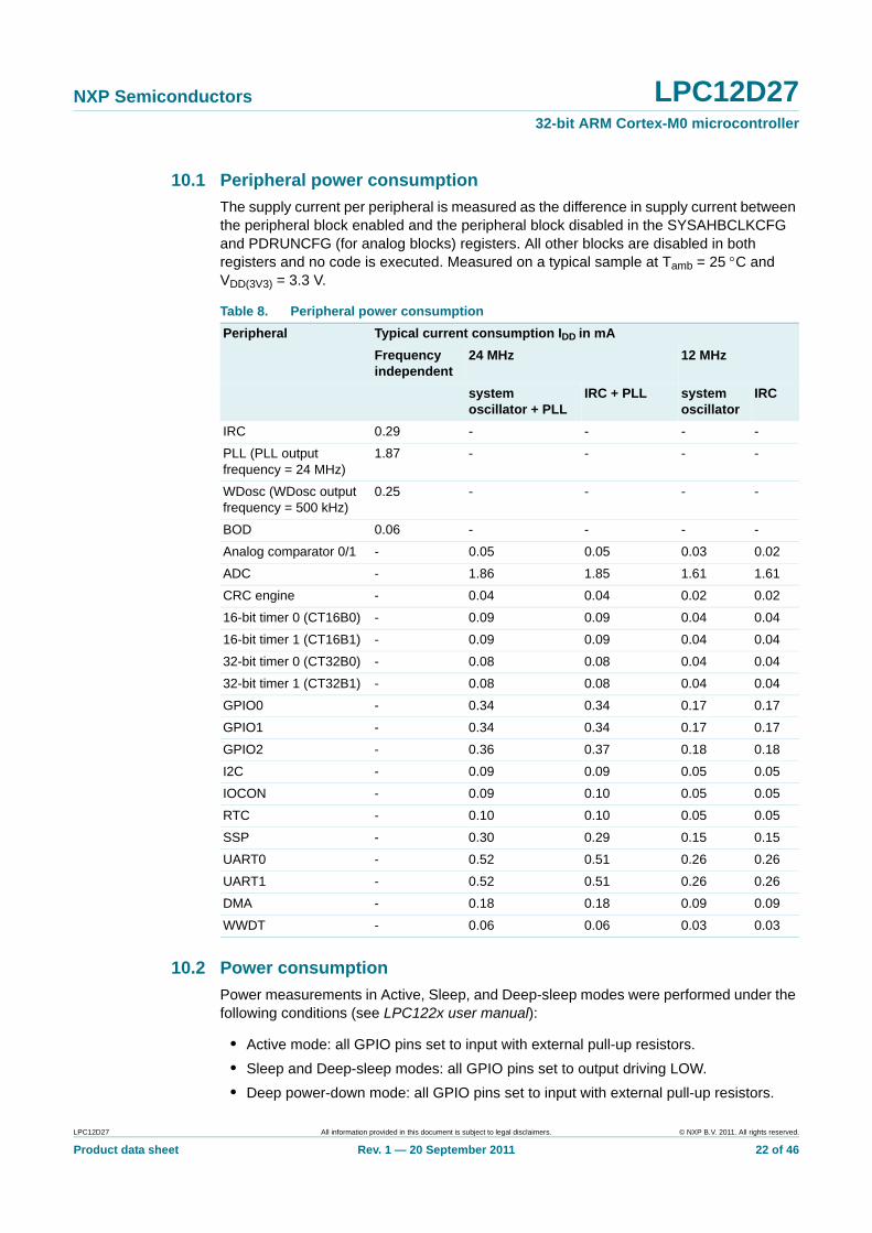
Conditions: Tamb = 25 C; active mode entered executing code while(1){} from flash; all peripherals disabled in the SYSAHBCLKCTRL register; all peripheral clocks disabled; internal pull-up resistors disabled; BOD disabled.
(1) System oscillator and system PLL disabled; IRC enabled.
(2) System oscillator and system PLL enabled; IRC disabled.
(3) System oscillator enabled; IRC and system PLL disabled.
Fig 5. Active mode: Typical supply current IDD versus supply voltage VDD(3V3) for different system clock frequencies (all peripherals disabled)
Conditions: VDD(3V3) = 3.3 V; active mode entered executing code while(1){} from flash; all peripherals disabled in the SYSAHBCLKCTRL register; all peripheral clocks disabled; internal pull-up resistors disabled; BOD disabled.
(1) System oscillator and system PLL disabled; IRC enabled.
(2) System oscillator and system PLL enabled; IRC disabled.
(3) System oscillator enabled; IRC and system PLL disabled.
Fig 6. Active mode: Typical supply current IDD versus temperature for different system clock frequencies (peripherals disabled)
VDD(3V3) (V)3 3.63.43.2
002aag186
8
4
12
16
IDD(mA)
0
33 MHz(2)
24 MHz(2)
12 MHz(1)
4 MHz(3)
1 MHz(3)
12 MHz(1)
4 MHz(3)
1 MHz(3)
33 MHz(2)
24 MHz(2)
002aag023
temperature (°C)-40 853510 60-15
4
12
8
16
IDD(mA)
0
LPC12D27 All information provided in this document is subject to legal disclaimers. © NXP B.V. 2011. All rights reserved.
Product data sheet Rev. 1 — 20 September 2011 23 of 46
NXP Semiconductors LPC12D2732-bit ARM Cortex-M0 microcontroller
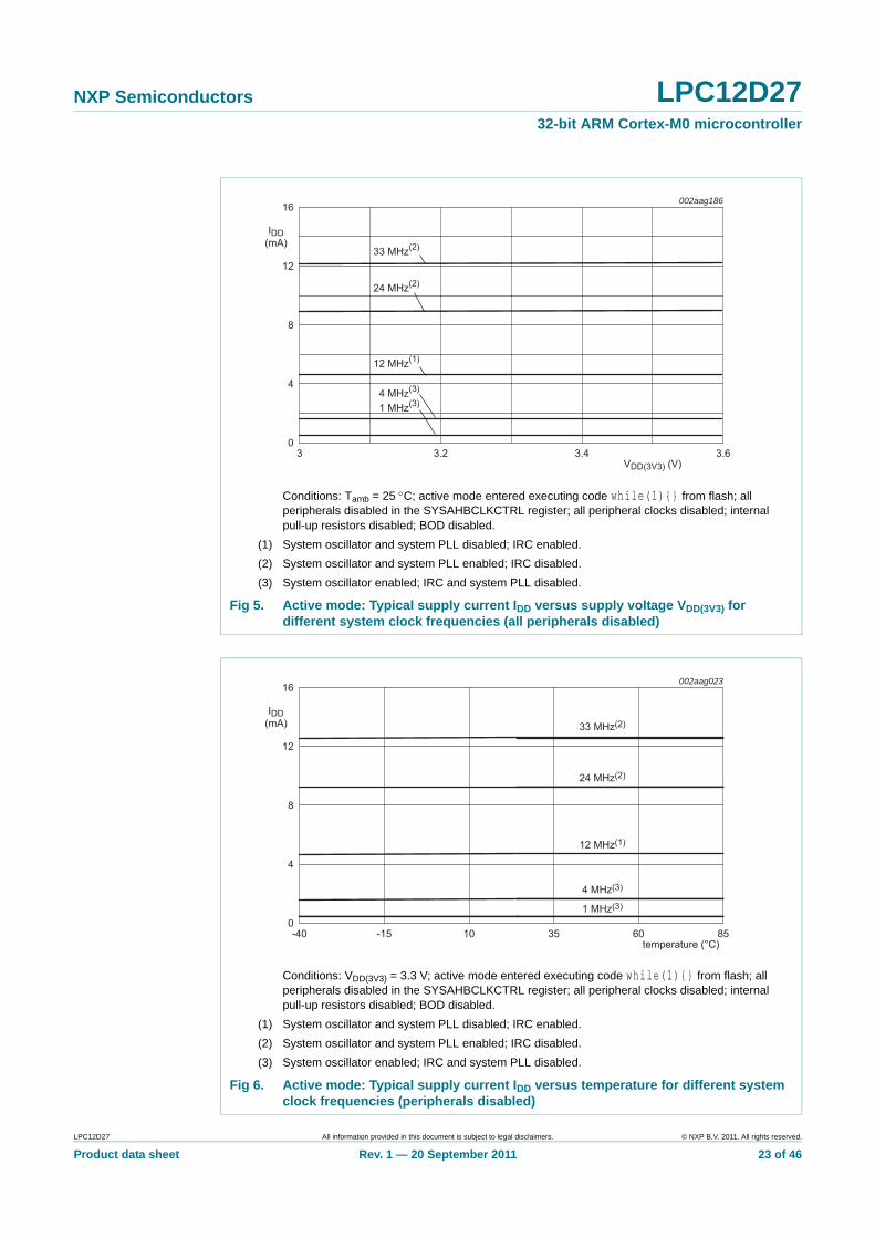
Conditions: Tamb = 25 C; active mode entered executing code while(1){} from flash; all peripherals enabled in the SYSAHBCLKCTRL register.
(1) System oscillator and system PLL disabled; IRC enabled.
(2) System oscillator and system PLL enabled; IRC disabled.
(3) System oscillator enabled with external clock input; IRC and system PLL disabled.
Fig 7. Active mode: Typical supply current IDD versus supply voltage VDD(3V3) for different system clock frequencies (all peripherals enabled)
Conditions: VDD(3V3) = 3.3 V; active mode entered executing code while(1){} from flash; all peripherals enabled in the SYSAHBCLKCTRL register.
(1) System oscillator and system PLL disabled; IRC enabled.
(2) System oscillator and system PLL enabled; IRC disabled.
(3) System oscillator enabled with external clock input; IRC and system PLL disabled.
Fig 8. Active mode: Typical supply current IDD versus temperature for different system clock frequencies (peripherals enabled)
VDD(3V3) (V)3 3.63.43.2
002aag187
8
4
12
16
IDD(mA)
0
33 MHz(2)
24 MHz(2)
12 MHz(1)
4 MHz(3)
1 MHz(3)
12 MHz(1)
4 MHz(3)
1 MHz(3)
33 MHz(2)
24 MHz(2)
002aag024
temperature (°C)-40 853510 60-15
4
12
8
16
IDD(mA)
0
LPC12D27 All information provided in this document is subject to legal disclaimers. © NXP B.V. 2011. All rights reserved.
Product data sheet Rev. 1 — 20 September 2011 24 of 46
NXP Semiconductors LPC12D2732-bit ARM Cortex-M0 microcontroller
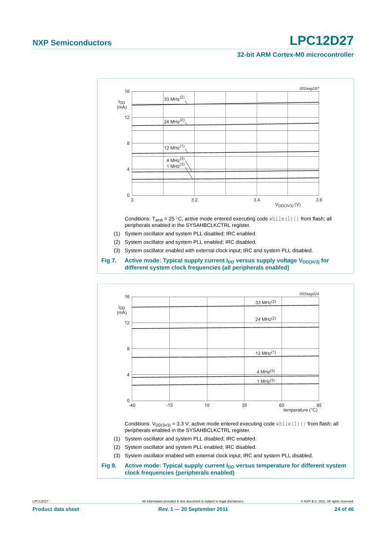
Conditions: VDD(3V3) = 3.3 V; sleep mode entered from flash; all peripherals disabled in the SYSAHBCLKCTRL register (SYSAHBCLKCTRL = 0x1F); all peripheral clocks disabled; internal pull-up resistors disabled; BOD disabled.
(1) System oscillator and system PLL disabled; IRC enabled.
(2) System oscillator and system PLL enabled; IRC disabled.
(3) System oscillator enabled with external clock input; IRC and system PLL disabled.
Fig 9. Sleep mode: Typical supply current IDD versus supply voltage VDD(3V3) for different system clock frequencies
Conditions: BOD disabled; all oscillators and analog blocks disabled in the PDSLEEPCFG register
Fig 10. Deep-sleep mode: Typical supply current IDD versus temperature for different supply voltages VDD(3V3)
VDD(3V3) (V)3.0 3.63.43.2
002aag188
2
3
1
4
5
IDD(mA)
0
33 MHz(2)
24 MHz(2)
12 MHz(1)
1 MHz(3)4 MHz(3)
002aag190
20
40
30
50
IDD(μA)
10
temperature (°C)-40 853510 60-15
VDD(3V3) = 3.6 V3.3 V3.0 V
LPC12D27 All information provided in this document is subject to legal disclaimers. © NXP B.V. 2011. All rights reserved.
Product data sheet Rev. 1 — 20 September 2011 25 of 46
NXP Semiconductors LPC12D2732-bit ARM Cortex-M0 microcontroller
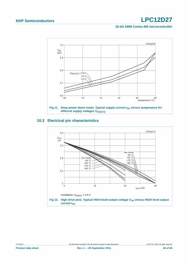
10.3 Electrical pin characteristics
Fig 11. Deep power-down mode: Typical supply current IDD versus temperature for different supply voltages VDD(3V3)
002aag189
0.7
0.9
0.8
1.0
IDD(μA)
0.6
temperature (°C)-40 853510 60-15
VDD(3V3) = 3.6 V3.3 V3.0 V
Conditions: VDD(IO) = 3.3 V
Fig 12. High-drive pins: Typical HIGH-level output voltage VOH versus HIGH-level output current IOH
IOH (mA)0 483216
002aag175
2.8
2.4
3.2
3.6
VOH(V)
2
low mode-40 °C+25 °C+70 °C+85 °C
low mode-40 °C+25 °C+70 °C+85 °C
LPC12D27 All information provided in this document is subject to legal disclaimers. © NXP B.V. 2011. All rights reserved.
Product data sheet Rev. 1 — 20 September 2011 26 of 46
NXP Semiconductors LPC12D2732-bit ARM Cortex-M0 microcontroller
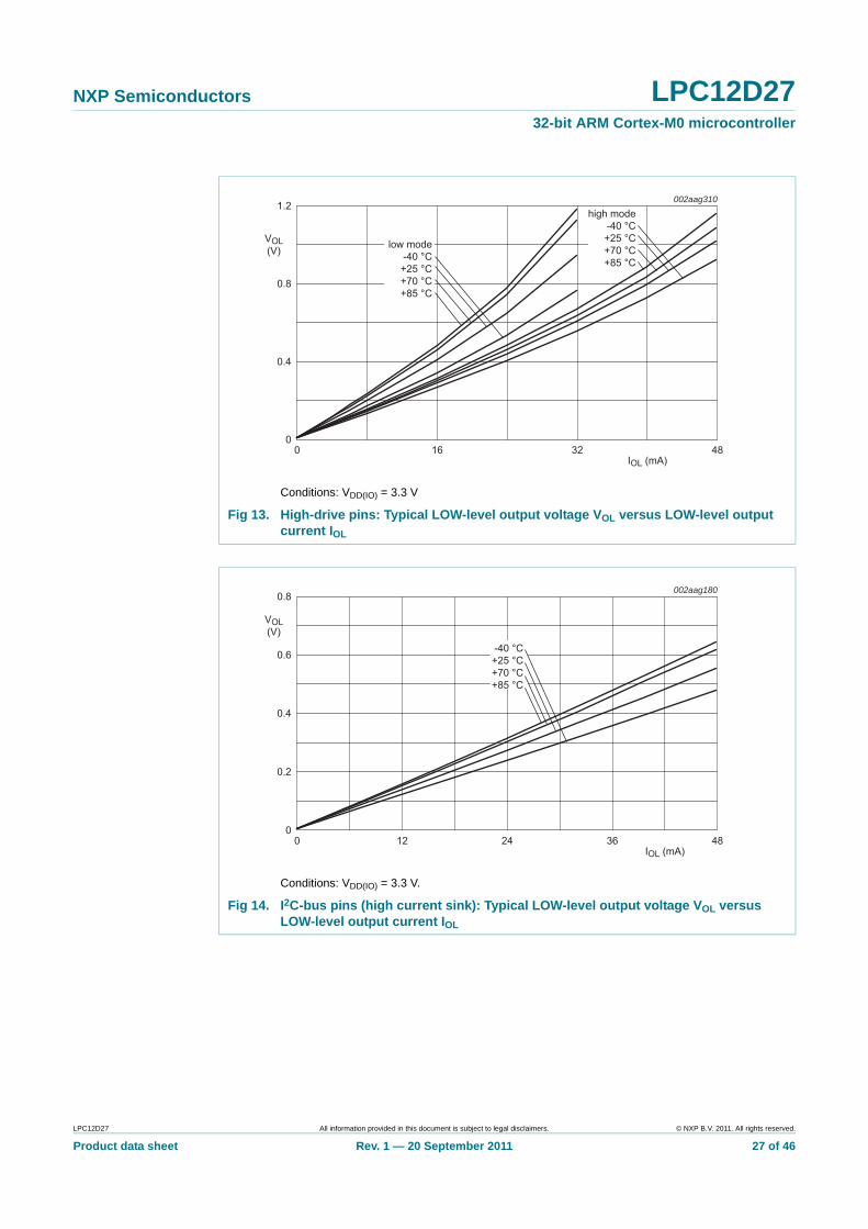
Conditions: VDD(IO) = 3.3 V
Fig 13. High-drive pins: Typical LOW-level output voltage VOL versus LOW-level output current IOL
Conditions: VDD(IO) = 3.3 V.
Fig 14. I2C-bus pins (high current sink): Typical LOW-level output voltage VOL versus LOW-level output current IOL
IOL (mA)0 483216
002aag310
0.4
0.8
1.2
VOL(V)
0
low mode-40 °C+25 °C+70 °C+85 °C
high mode-40 °C+25 °C+70 °C+85 °C
IOL (mA)0 48362412
002aag180
0.4
0.2
0.6
0.8
VOL(V)
0
-40 °C+25 °C+70 °C+85 °C
LPC12D27 All information provided in this document is subject to legal disclaimers. © NXP B.V. 2011. All rights reserved.
Product data sheet Rev. 1 — 20 September 2011 27 of 46
NXP Semiconductors LPC12D2732-bit ARM Cortex-M0 microcontroller
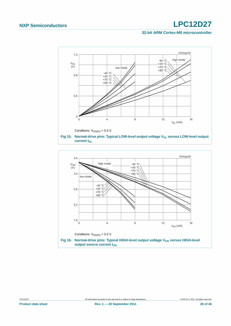
Conditions: VDD(IO) = 3.3 V.
Fig 15. Normal-drive pins: Typical LOW-level output voltage VOL versus LOW-level output current IOL
Conditions: VDD(IO) = 3.3 V.
Fig 16. Normal-drive pins: Typical HIGH-level output voltage VOH versus HIGH-level output source current IOH
002aag181
IOL (mA)0 161284
0.4
0.8
1.2
VOL(V)
0
-40 °C+25 °C+70 °C+85 °C
-40 °C+25 °C+70 °C+85 °C
low mode
high mode
IOH (mA)0 161284
002aag182
2.6
2.2
3.0
3.4
VOH(V)
1.8
-40 °C+25 °C+70 °C+85 °C
-40 °C+25 °C+70 °C+85 °C
low mode
high mode
LPC12D27 All information provided in this document is subject to legal disclaimers. © NXP B.V. 2011. All rights reserved.
Product data sheet Rev. 1 — 20 September 2011 28 of 46
NXP Semiconductors LPC12D2732-bit ARM Cortex-M0 microcontroller
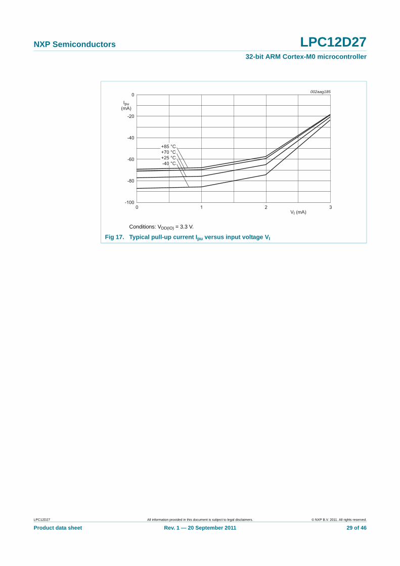
Conditions: VDD(IO) = 3.3 V.
Fig 17. Typical pull-up current Ipu versus input voltage VI
VI (mA)0 321
002aag185
-60
-40
-80
-20
0
Ipu(mA)
-100
+85 °C+70 °C+25 °C-40 °C
LPC12D27 All information provided in this document is subject to legal disclaimers. © NXP B.V. 2011. All rights reserved.
Product data sheet Rev. 1 — 20 September 2011 29 of 46
NXP Semiconductors LPC12D2732-bit ARM Cortex-M0 microcontroller
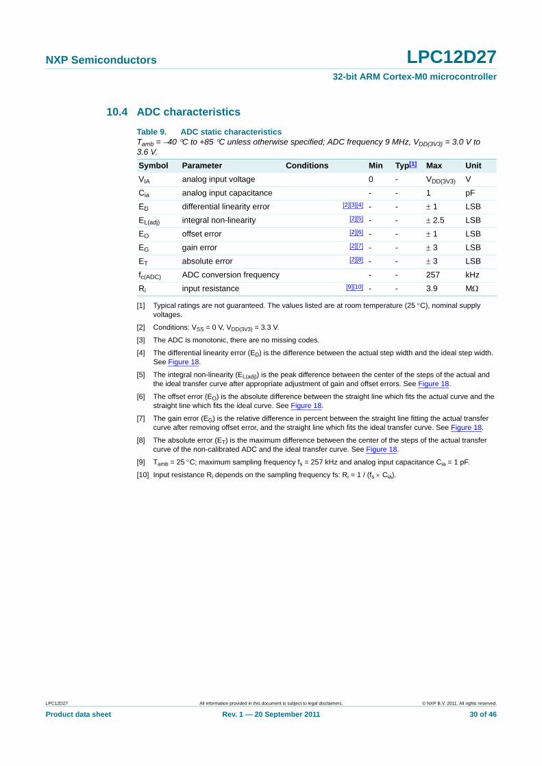
10.4 ADC characteristics
[1] Typical ratings are not guaranteed. The values listed are at room temperature (25 C), nominal supply voltages.
[2] Conditions: VSS = 0 V, VDD(3V3) = 3.3 V.
[3] The ADC is monotonic, there are no missing codes.
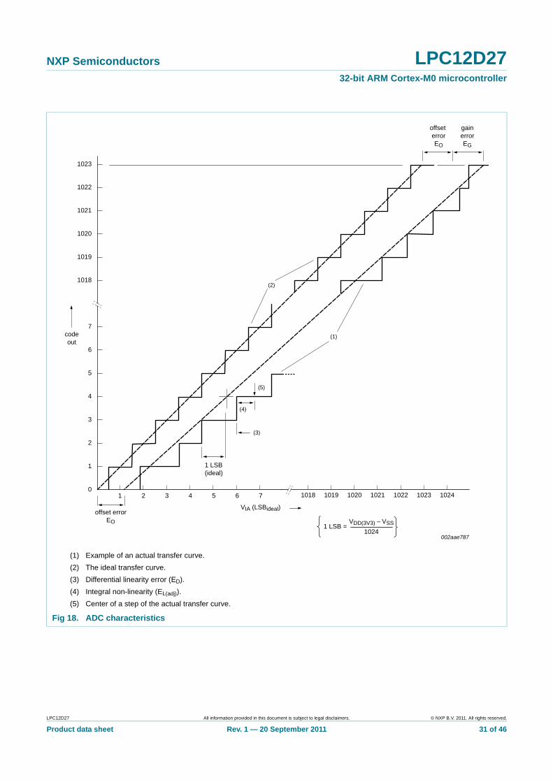
[4] The differential linearity error (ED) is the difference between the actual step width and the ideal step width. See Figure 18.
[5] The integral non-linearity (EL(adj)) is the peak difference between the center of the steps of the actual and the ideal transfer curve after appropriate adjustment of gain and offset errors. See Figure 18.
[6] The offset error (EO) is the absolute difference between the straight line which fits the actual curve and the straight line which fits the ideal curve. See Figure 18.
[7] The gain error (EG) is the relative difference in percent between the straight line fitting the actual transfer curve after removing offset error, and the straight line which fits the ideal transfer curve. See Figure 18.
[8] The absolute error (ET) is the maximum difference between the center of the steps of the actual transfer curve of the non-calibrated ADC and the ideal transfer curve. See Figure 18.
[9] Tamb = 25 C; maximum sampling frequency fs = 257 kHz and analog input capacitance Cia = 1 pF.
[10] Input resistance Ri depends on the sampling frequency fs: Ri = 1 / (fs Cia).
Table 9. ADC static characteristicsTamb = 40 C to +85 C unless otherwise specified; ADC frequency 9 MHz, VDD(3V3) = 3.0 V to 3.6 V.
Symbol Parameter Conditions Min Typ[1] Max Unit
VIA analog input voltage 0 - VDD(3V3) V
Cia analog input capacitance - - 1 pF
ED differential linearity error [2][3][4] - - 1 LSB
EL(adj) integral non-linearity [2][5] - - 2.5 LSB
EO offset error [2][6] - - 1 LSB
EG gain error [2][7] - - 3 LSB
ET absolute error [2][8] - - 3 LSB
fc(ADC) ADC conversion frequency - - 257 kHz
Ri input resistance [9][10] - - 3.9 M
LPC12D27 All information provided in this document is subject to legal disclaimers. © NXP B.V. 2011. All rights reserved.
Product data sheet Rev. 1 — 20 September 2011 30 of 46
NXP Semiconductors LPC12D2732-bit ARM Cortex-M0 microcontroller
(1) Example of an actual transfer curve.
(2) The ideal transfer curve.
(3) Differential linearity error (ED).
(4) Integral non-linearity (EL(adj)).
(5) Center of a step of the actual transfer curve.
Fig 18. ADC characteristics
002aae787
1023
1022
1021
1020
1019
(2)
(1)
10241018 1019 1020 1021 1022 102371 2 3 4 5 6
7
6
5
4
3
2
1
0
1018
(5)
(4)
(3)
1 LSB(ideal)
codeout
VDD(3V3) − VSS
1024
offset errorEO
gainerrorEG
offset errorEO
VIA (LSBideal)
1 LSB =
LPC12D27 All information provided in this document is subject to legal disclaimers. © NXP B.V. 2011. All rights reserved.
Product data sheet Rev. 1 — 20 September 2011 31 of 46
NXP Semiconductors LPC12D2732-bit ARM Cortex-M0 microcontroller
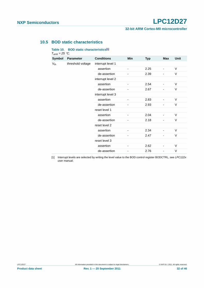
10.5 BOD static characteristics
[1] Interrupt levels are selected by writing the level value to the BOD control register BODCTRL, see LPC122x user manual.
Table 10. BOD static characteristics[1]
Tamb = 25 C.
Symbol Parameter Conditions Min Typ Max Unit
Vth threshold voltage interrupt level 1
assertion - 2.25 - V
de-assertion - 2.39 - V
interrupt level 2
assertion - 2.54 - V
de-assertion - 2.67 - V
interrupt level 3
assertion - 2.83 - V
de-assertion - 2.93 - V
reset level 1
assertion - 2.04 - V
de-assertion - 2.18 - V
reset level 2
assertion - 2.34 - V
de-assertion - 2.47 - V
reset level 3
assertion - 2.62 - V
de-assertion - 2.76 - V
LPC12D27 All information provided in this document is subject to legal disclaimers. © NXP B.V. 2011. All rights reserved.
Product data sheet Rev. 1 — 20 September 2011 32 of 46
NXP Semiconductors LPC12D2732-bit ARM Cortex-M0 microcontroller
11. Dynamic characteristics
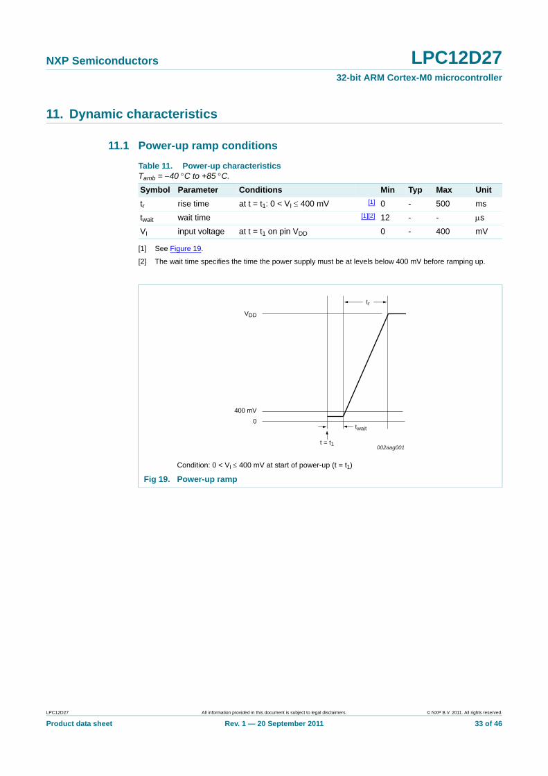
11.1 Power-up ramp conditions
[1] See Figure 19.
[2] The wait time specifies the time the power supply must be at levels below 400 mV before ramping up.
Table 11. Power-up characteristicsTamb = 40 C to +85 C.
Symbol Parameter Conditions Min Typ Max Unit
tr rise time at t = t1: 0 < VI 400 mV [1] 0 - 500 ms
twait wait time [1][2] 12 - - s
VI input voltage at t = t1 on pin VDD 0 - 400 mV
Condition: 0 < VI 400 mV at start of power-up (t = t1)
Fig 19. Power-up ramp
VDD
0
400 mV
tr
twait
t = t1002aag001
LPC12D27 All information provided in this document is subject to legal disclaimers. © NXP B.V. 2011. All rights reserved.
Product data sheet Rev. 1 — 20 September 2011 33 of 46
NXP Semiconductors LPC12D2732-bit ARM Cortex-M0 microcontroller
11.2 Flash memory
[1] Erase and programming times are valid over the lifetime of the device (minimum 20000 cycles).
[2] Number of program/erase cycles.
11.3 External clock
[1] Parameters are valid over operating temperature range unless otherwise specified.
[2] Typical ratings are not guaranteed. The values listed are at room temperature (25 C), nominal supply voltages.
Table 12. Dynamic characteristics: flash memoryTamb = 40 C to +85 C; VDD(3V3) over specified ranges.
Symbol Parameter Conditions Min Max Unit
ter erase time for one page (512 byte) [1] - 20 ms
for one sector (4 kB) [1] 162 ms
for all sectors; mass erase
[1] - 20 ms
tprog programming time
one word (4 bytes) [1] - 49 s
four sequential words [1] - 194 s
128 bytes (one row of 32 words)
[1] - 765 s
Nendu endurance [2] 20000 - cycles
tret retention time 10 - years
Table 13. Dynamic characteristics: external clockTamb = 40 C to +85 C; VDD(3V3) over specified ranges.[1]
Symbol Parameter Conditions Min Typ[2] Max Unit
fosc oscillator frequency 1 - 25 MHz
Tcy(clk) clock cycle time 40 - 1000 ns
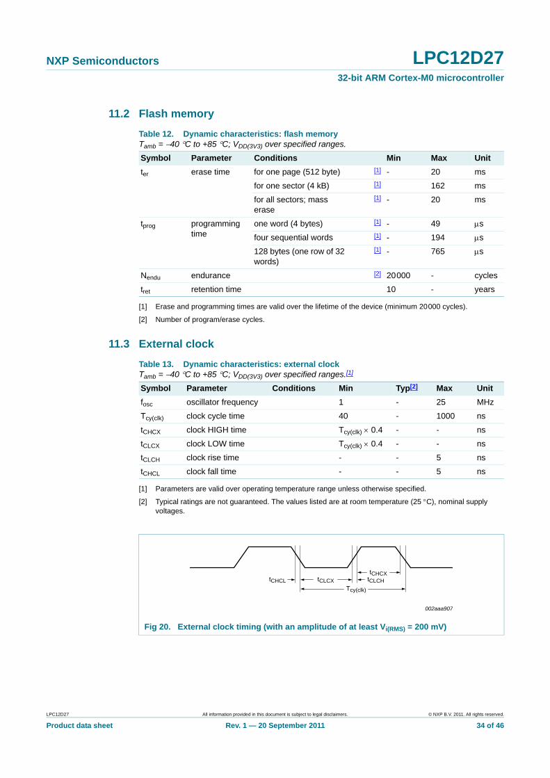
tCHCX clock HIGH time Tcy(clk) 0.4 - - ns
tCLCX clock LOW time Tcy(clk) 0.4 - - ns
tCLCH clock rise time - - 5 ns
tCHCL clock fall time - - 5 ns
Fig 20. External clock timing (with an amplitude of at least Vi(RMS) = 200 mV)
tCHCL tCLCX
tCHCX
Tcy(clk)
tCLCH
002aaa907
LPC12D27 All information provided in this document is subject to legal disclaimers. © NXP B.V. 2011. All rights reserved.
Product data sheet Rev. 1 — 20 September 2011 34 of 46
NXP Semiconductors LPC12D2732-bit ARM Cortex-M0 microcontroller
11.4 Internal oscillators
[1] Parameters are valid over operating temperature range unless otherwise specified.
[2] Typical ratings are not guaranteed. The values listed are at nominal supply voltages.
[1] Typical ratings are not guaranteed. The values listed are at room temperature (25 C), nominal supply voltages.
[2] The typical frequency spread over processing and temperature (Tamb = 40 C to +85 C) is 40 %.
[3] See the LPC122x user manual.
Table 14. Dynamic characteristics: internal oscillatorsTamb = 40 C to +85 C; VDD(3V3) over specified ranges.[1]
Symbol Parameter Conditions Min Typ[2] Max Unit
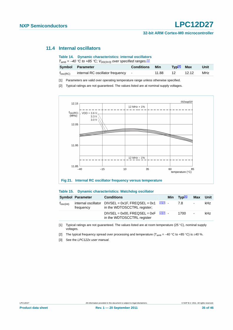
fosc(RC) internal RC oscillator frequency - 11.88 12 12.12 MHz
Fig 21. Internal RC oscillator frequency versus temperature
Table 15. Dynamic characteristics: Watchdog oscillator
Symbol Parameter Conditions Min Typ[1] Max Unit
fosc(int) internal oscillator frequency
DIVSEL = 0x1F, FREQSEL = 0x1 in the WDTOSCCTRL register;
[2][3] - 7.8 - kHz
DIVSEL = 0x00, FREQSEL = 0xF in the WDTOSCCTRL register
[2][3] - 1700 - kHz
002aag020
11.95
12.05
12.15
fosc(RC)(MHz)
11.85
temperature (°C)−40 853510 60−15
VDD = 3.6 V3.3 V3.0 V
12 MHz + 1%
12 MHz − 1%
LPC12D27 All information provided in this document is subject to legal disclaimers. © NXP B.V. 2011. All rights reserved.
Product data sheet Rev. 1 — 20 September 2011 35 of 46
NXP Semiconductors LPC12D2732-bit ARM Cortex-M0 microcontroller
11.5 I2C-bus
[1] Parameters are valid over operating temperature range unless otherwise specified.
[2] A device must internally provide a hold time of at least 300 ns for the SDA signal (with respect to the VIH(min) of the SCL signal) to bridge the undefined region of the falling edge of SCL.
[3] Cb = total capacitance of one bus line in pF. If mixed with Hs-mode devices, faster fall times are allowed.
[4] The maximum tf for the SDA and SCL bus lines is specified at 300 ns. The maximum fall time for the SDA output stage tf is specified at
250 ns. This allows series protection resistors to be connected in between the SDA and the SCL pins and the SDA/SCL bus lines
without exceeding the maximum specified tf.
[5] In Fast-mode Plus, fall time is specified the same for both output stage and bus timing. If series resistors are used, designers should
allow for this when considering bus timing.
[6] tHD;DAT is the data hold time that is measured from the falling edge of SCL; applies to data in transmission and the acknowledge.
[7] The maximum tHD;DAT could be 3.45 s and 0.9 s for Standard-mode and Fast-mode but must be less than the maximum of tVD;DAT or tVD;ACK by a transition time. This maximum must only be met if the device does not stretch the LOW period (tLOW) of the SCL signal. If the clock stretches the SCL, the data must be valid by the set-up time before it releases the clock.
[8] tSU;DAT is the data set-up time that is measured with respect to the rising edge of SCL; applies to data in transmission and the acknowledge.
[9] A Fast-mode I2C-bus device can be used in a Standard-mode I2C-bus system but the requirement tSU;DAT = 250 ns must then be met. This will automatically be the case if the device does not stretch the LOW period of the SCL signal. If such a device does stretch the LOW period of the SCL signal, it must output the next data bit to the SDA line tr(max) + tSU;DAT = 1000 + 250 = 1250 ns (according to the Standard-mode I2C-bus specification) before the SCL line is released. Also the acknowledge timing must meet this set-up time.
Table 16. Dynamic characteristics: I2C-bus pinsTamb = 40 C to +85 C.[1]
Symbol Parameter Conditions Min Max Unit
fSCL SCL clock frequency
Standard-mode 0 100 kHz
Fast-mode 0 400 kHz
Fast-mode Plus 0 1 MHz
tf fall time [2][3][4][5] of both SDA and SCL signals
Standard-mode
- 300 ns
Fast-mode 20 + 0.1 Cb 300 ns
Fast-mode Plus
- 120 ns
tLOW LOW period of the SCL clock
Standard-mode 4.7 - s
Fast-mode 1.3 - s
Fast-mode Plus 0.5 - s
tHIGH HIGH period of the SCL clock
Standard-mode 4.0 - s
Fast-mode 0.6 - s
Fast-mode Plus 0.26 - s
tHD;DAT data hold time [6][2][7] Standard-mode 0 - s
Fast-mode 0 - s
Fast-mode Plus 0 - s
tSU;DAT data set-up time
[8][9] Standard-mode 250 - ns
Fast-mode 100 - ns
Fast-mode Plus 50 - ns
LPC12D27 All information provided in this document is subject to legal disclaimers. © NXP B.V. 2011. All rights reserved.
Product data sheet Rev. 1 — 20 September 2011 36 of 46
NXP Semiconductors LPC12D2732-bit ARM Cortex-M0 microcontroller
Fig 22. I2C-bus pins clock timing
002aaf425
tf
70 %30 %SDA
tf
70 %30 %
S
70 %30 %
70 %30 %
tHD;DAT
SCL
1 / fSCL
70 %30 %
70 %30 %
tVD;DAT
tHIGH
tLOW
tSU;DAT
LPC12D27 All information provided in this document is subject to legal disclaimers. © NXP B.V. 2011. All rights reserved.
Product data sheet Rev. 1 — 20 September 2011 37 of 46
NXP Semiconductors LPC12D2732-bit ARM Cortex-M0 microcontroller
12. Application information
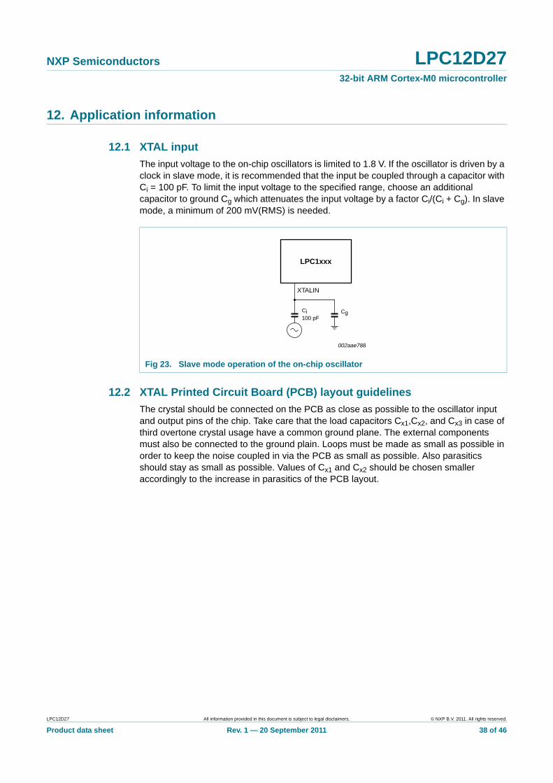
12.1 XTAL input
The input voltage to the on-chip oscillators is limited to 1.8 V. If the oscillator is driven by a clock in slave mode, it is recommended that the input be coupled through a capacitor with Ci = 100 pF. To limit the input voltage to the specified range, choose an additional capacitor to ground Cg which attenuates the input voltage by a factor Ci/(Ci + Cg). In slave mode, a minimum of 200 mV(RMS) is needed.
12.2 XTAL Printed Circuit Board (PCB) layout guidelines
The crystal should be connected on the PCB as close as possible to the oscillator input and output pins of the chip. Take care that the load capacitors Cx1,Cx2, and Cx3 in case of third overtone crystal usage have a common ground plane. The external components must also be connected to the ground plain. Loops must be made as small as possible in order to keep the noise coupled in via the PCB as small as possible. Also parasitics should stay as small as possible. Values of Cx1 and Cx2 should be chosen smaller accordingly to the increase in parasitics of the PCB layout.
Fig 23. Slave mode operation of the on-chip oscillator
LPC1xxx
XTALIN
Ci100 pF
Cg
002aae788
LPC12D27 All information provided in this document is subject to legal disclaimers. © NXP B.V. 2011. All rights reserved.
Product data sheet Rev. 1 — 20 September 2011 38 of 46
NXP Semiconductors LPC12D2732-bit ARM Cortex-M0 microcontroller
12.3 ElectroMagnetic Compatibility (EMC)
Radiated emission measurements according to the IEC61967-2 standard using the TEM-cell method are shown for the LPC1227FBD64/301 in Table 17.
[1] IEC levels refer to Appendix D in the IEC61967-2 Specification.
Table 17. ElectroMagnetic Compatibility (EMC) for part LPC1227FBD64/301 (TEM-cell method)
VDD = 3.3 V; Tamb = 25 C.
Parameter Frequency band System clock = Unit
12 MHz 24 MHz 33 MHz
Input clock: IRC (12 MHz)
maximum peak level
150 kHz - 30 MHz 4.2 3.8 6.4 dBV
30 MHz - 150 MHz 7.3 5.4 9 dBV
150 MHz - 1 GHz 16.4 20.1 23.4 dBV
IEC level[1] - M L L -
Input clock: crystal oscillator (12 MHz)
maximum peak level
150 kHz - 30 MHz 4.8 4 6.6 dBV
30 MHz - 150 MHz 6.9 5.6 10 dBV
150 MHz - 1 GHz 16.3 20.3 22.3 dBV
IEC level[1] - M L L -
LPC12D27 All information provided in this document is subject to legal disclaimers. © NXP B.V. 2011. All rights reserved.
Product data sheet Rev. 1 — 20 September 2011 39 of 46
NXP Semiconductors LPC12D2732-bit ARM Cortex-M0 microcontroller
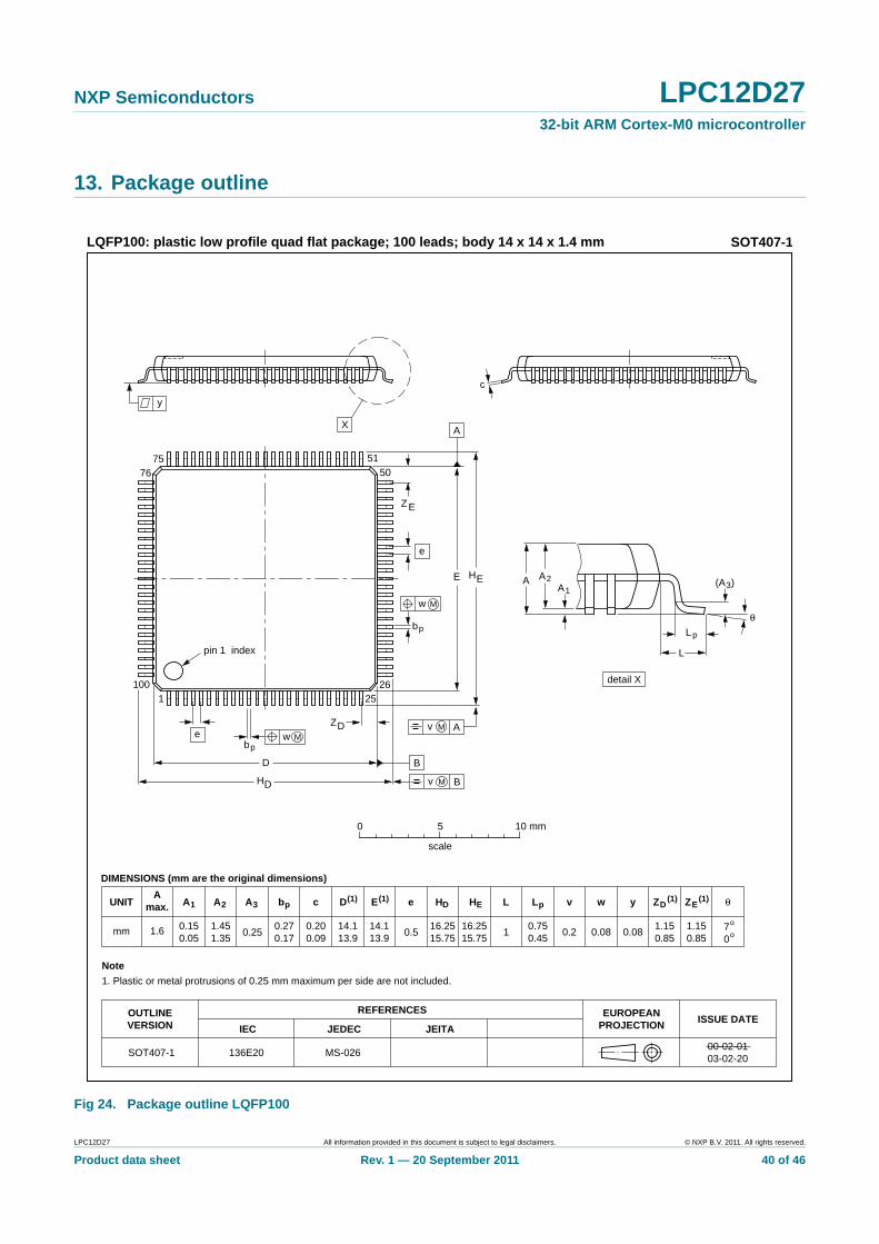
13. Package outline
Fig 24. Package outline LQFP100
UNITA
max. A1 A2 A3 bp c E(1) e HE L Lp Zywv θ
REFERENCESOUTLINEVERSION
EUROPEANPROJECTION ISSUE DATE
IEC JEDEC JEITA
mm 1.6 0.150.05
1.451.35
0.250.270.17
0.200.09
14.113.9
0.516.2515.75
1.150.85
70
o
o0.08 0.080.21
DIMENSIONS (mm are the original dimensions)
Note
1. Plastic or metal protrusions of 0.25 mm maximum per side are not included.
0.750.45
SOT407-1 136E20 MS-02600-02-0103-02-20
D(1) (1)(1)
14.113.9
HD
16.2515.75
EZ
1.150.85
D
bp
e
θ
EA1
A
L p
detail X
L
(A )3
B
25
c
DH
bp
EH A2
v M B
D
ZD
A
ZE
e
v M A
X
1100
7675 51
50
26
y
pin 1 index
w M
w M
0 5 10 mm
scale
LQFP100: plastic low profile quad flat package; 100 leads; body 14 x 14 x 1.4 mm SOT407-1
LPC12D27 All information provided in this document is subject to legal disclaimers. © NXP B.V. 2011. All rights reserved.
Product data sheet Rev. 1 — 20 September 2011 40 of 46
NXP Semiconductors LPC12D2732-bit ARM Cortex-M0 microcontroller
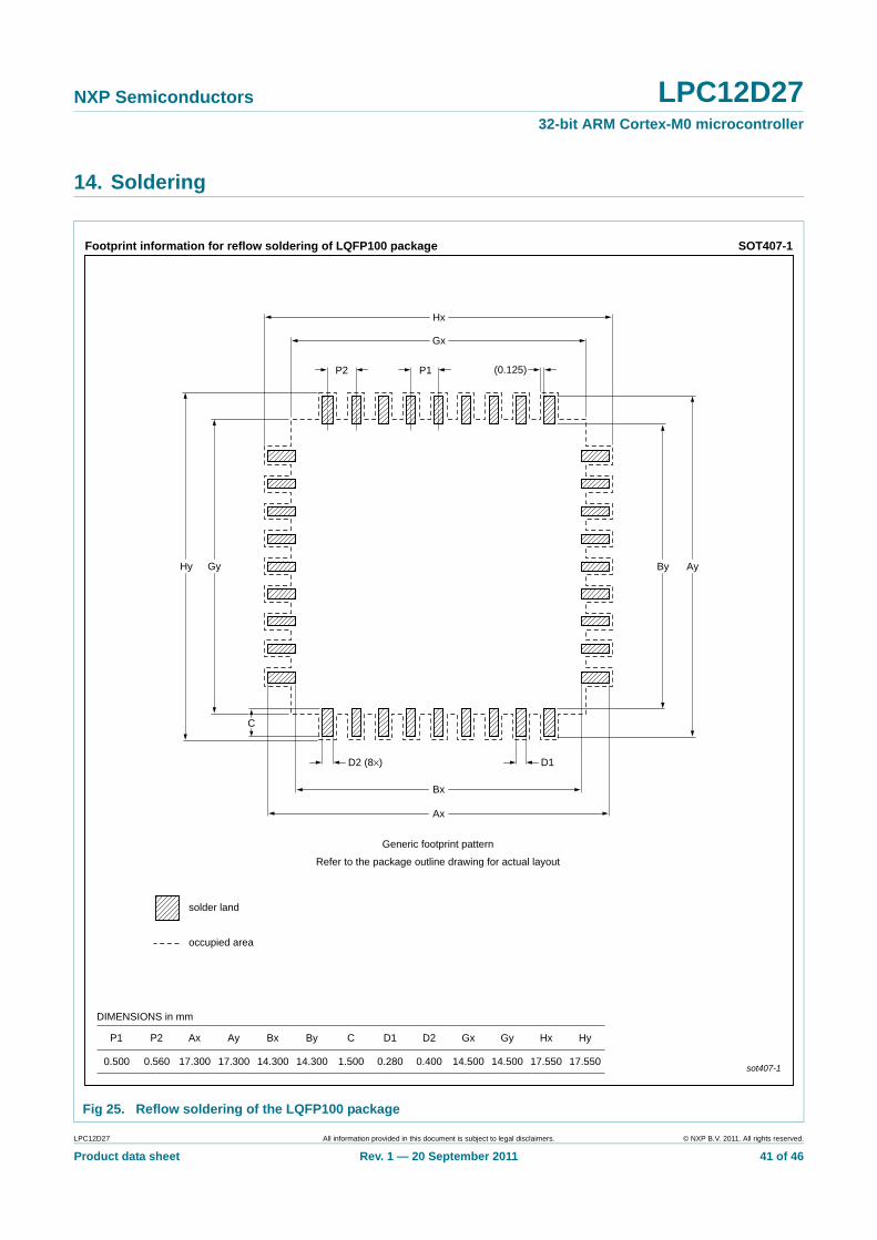
14. Soldering
Fig 25. Reflow soldering of the LQFP100 package
SOT407-1
DIMENSIONS in mm
occupied area
Footprint information for reflow soldering of LQFP100 package
Ax
Bx
Gx
GyHy
Hx
AyBy
P1P2
D2 (8×) D1
(0.125)
Ax Ay Bx By D1 D2 Gx Gy Hx HyP1 P2 C
sot407-1
solder land
C
Generic footprint pattern
Refer to the package outline drawing for actual layout
17.300 17.300 14.300 14.3000.500 0.560 0.2801.500 0.400 14.500 14.500 17.550 17.550
LPC12D27 All information provided in this document is subject to legal disclaimers. © NXP B.V. 2011. All rights reserved.
Product data sheet Rev. 1 — 20 September 2011 41 of 46
NXP Semiconductors LPC12D2732-bit ARM Cortex-M0 microcontroller
15. References
[1] LPC122x data sheet, http://www.nxp.com/microcontrollers
[2] PCF8576D data sheet, http://www.nxp.com/microcontrollers
LPC12D27 All information provided in this document is subject to legal disclaimers. © NXP B.V. 2011. All rights reserved.
Product data sheet Rev. 1 — 20 September 2011 42 of 46
NXP Semiconductors LPC12D2732-bit ARM Cortex-M0 microcontroller
16. Revision history
Table 18. Revision history
Document ID Release date Data sheet status Change notice Supersedes
LPC12D27 v.1 20110920 Product data sheet - -
LPC12D27 All information provided in this document is subject to legal disclaimers. © NXP B.V. 2011. All rights reserved.
Product data sheet Rev. 1 — 20 September 2011 43 of 46
NXP Semiconductors LPC12D2732-bit ARM Cortex-M0 microcontroller
17. Legal information
17.1 Data sheet status
[1] Please consult the most recently issued document before initiating or completing a design.
[2] The term ‘short data sheet’ is explained in section “Definitions”.
[3] The product status of device(s) described in this document may have changed since this document was published and may differ in case of multiple devices. The latest product status information is available on the Internet at URL http://www.nxp.com.
17.2 Definitions
Draft — The document is a draft version only. The content is still under internal review and subject to formal approval, which may result in modifications or additions. NXP Semiconductors does not give any representations or warranties as to the accuracy or completeness of information included herein and shall have no liability for the consequences of use of such information.
Short data sheet — A short data sheet is an extract from a full data sheet with the same product type number(s) and title. A short data sheet is intended for quick reference only and should not be relied upon to contain detailed and full information. For detailed and full information see the relevant full data sheet, which is available on request via the local NXP Semiconductors sales office. In case of any inconsistency or conflict with the short data sheet, the full data sheet shall prevail.
Product specification — The information and data provided in a Product data sheet shall define the specification of the product as agreed between NXP Semiconductors and its customer, unless NXP Semiconductors and customer have explicitly agreed otherwise in writing. In no event however, shall an agreement be valid in which the NXP Semiconductors product is deemed to offer functions and qualities beyond those described in the Product data sheet.
17.3 Disclaimers
Limited warranty and liability — Information in this document is believed to be accurate and reliable. However, NXP Semiconductors does not give any representations or warranties, expressed or implied, as to the accuracy or completeness of such information and shall have no liability for the consequences of use of such information.
In no event shall NXP Semiconductors be liable for any indirect, incidental, punitive, special or consequential damages (including - without limitation - lost profits, lost savings, business interruption, costs related to the removal or replacement of any products or rework charges) whether or not such damages are based on tort (including negligence), warranty, breach of contract or any other legal theory.
Notwithstanding any damages that customer might incur for any reason whatsoever, NXP Semiconductors’ aggregate and cumulative liability towards customer for the products described herein shall be limited in accordance with the Terms and conditions of commercial sale of NXP Semiconductors.
Right to make changes — NXP Semiconductors reserves the right to make changes to information published in this document, including without limitation specifications and product descriptions, at any time and without notice. This document supersedes and replaces all information supplied prior to the publication hereof.
Suitability for use — NXP Semiconductors products are not designed, authorized or warranted to be suitable for use in life support, life-critical or safety-critical systems or equipment, nor in applications where failure or
malfunction of an NXP Semiconductors product can reasonably be expected to result in personal injury, death or severe property or environmental damage. NXP Semiconductors accepts no liability for inclusion and/or use of NXP Semiconductors products in such equipment or applications and therefore such inclusion and/or use is at the customer’s own risk.
Applications — Applications that are described herein for any of these products are for illustrative purposes only. NXP Semiconductors makes no representation or warranty that such applications will be suitable for the specified use without further testing or modification.
Customers are responsible for the design and operation of their applications and products using NXP Semiconductors products, and NXP Semiconductors accepts no liability for any assistance with applications or customer product design. It is customer’s sole responsibility to determine whether the NXP Semiconductors product is suitable and fit for the customer’s applications and products planned, as well as for the planned application and use of customer’s third party customer(s). Customers should provide appropriate design and operating safeguards to minimize the risks associated with their applications and products.
NXP Semiconductors does not accept any liability related to any default, damage, costs or problem which is based on any weakness or default in the customer’s applications or products, or the application or use by customer’s third party customer(s). Customer is responsible for doing all necessary testing for the customer’s applications and products using NXP Semiconductors products in order to avoid a default of the applications and the products or of the application or use by customer’s third party customer(s). NXP does not accept any liability in this respect.
Limiting values — Stress above one or more limiting values (as defined in the Absolute Maximum Ratings System of IEC 60134) will cause permanent damage to the device. Limiting values are stress ratings only and (proper) operation of the device at these or any other conditions above those given in the Recommended operating conditions section (if present) or the Characteristics sections of this document is not warranted. Constant or repeated exposure to limiting values will permanently and irreversibly affect the quality and reliability of the device.
Terms and conditions of commercial sale — NXP Semiconductors products are sold subject to the general terms and conditions of commercial sale, as published at http://www.nxp.com/profile/terms, unless otherwise agreed in a valid written individual agreement. In case an individual agreement is concluded only the terms and conditions of the respective agreement shall apply. NXP Semiconductors hereby expressly objects to applying the customer’s general terms and conditions with regard to the purchase of NXP Semiconductors products by customer.
No offer to sell or license — Nothing in this document may be interpreted or construed as an offer to sell products that is open for acceptance or the grant, conveyance or implication of any license under any copyrights, patents or other industrial or intellectual property rights.
Export control — This document as well as the item(s) described herein may be subject to export control regulations. Export might require a prior authorization from national authorities.
Document status[1][2] Product status[3] Definition
Objective [short] data sheet Development This document contains data from the objective specification for product development.
Preliminary [short] data sheet Qualification This document contains data from the preliminary specification.
Product [short] data sheet Production This document contains the product specification.
LPC12D27 All information provided in this document is subject to legal disclaimers. © NXP B.V. 2011. All rights reserved.
Product data sheet Rev. 1 — 20 September 2011 44 of 46
NXP Semiconductors LPC12D2732-bit ARM Cortex-M0 microcontroller
Non-automotive qualified products — Unless this data sheet expressly states that this specific NXP Semiconductors product is automotive qualified, the product is not suitable for automotive use. It is neither qualified nor tested in accordance with automotive testing or application requirements. NXP Semiconductors accepts no liability for inclusion and/or use of non-automotive qualified products in automotive equipment or applications.
In the event that customer uses the product for design-in and use in automotive applications to automotive specifications and standards, customer (a) shall use the product without NXP Semiconductors’ warranty of the product for such automotive applications, use and specifications, and (b) whenever customer uses the product for automotive applications beyond NXP Semiconductors’ specifications such use shall be solely at customer’s
own risk, and (c) customer fully indemnifies NXP Semiconductors for any liability, damages or failed product claims resulting from customer design and use of the product for automotive applications beyond NXP Semiconductors’ standard warranty and NXP Semiconductors’ product specifications.
17.4 TrademarksNotice: All referenced brands, product names, service names and trademarks are the property of their respective owners.
I2C-bus — logo is a trademark of NXP B.V.
18. Contact information
For more information, please visit: http://www.nxp.com
For sales office addresses, please send an email to: [email protected]
LPC12D27 All information provided in this document is subject to legal disclaimers. © NXP B.V. 2011. All rights reserved.
Product data sheet Rev. 1 — 20 September 2011 45 of 46
NXP Semiconductors LPC12D2732-bit ARM Cortex-M0 microcontroller
19. Contents
1 General description . . . . . . . . . . . . . . . . . . . . . . 1
2 Features and benefits . . . . . . . . . . . . . . . . . . . . 1
3 Applications . . . . . . . . . . . . . . . . . . . . . . . . . . . . 3
4 Ordering information. . . . . . . . . . . . . . . . . . . . . 34.1 Ordering options . . . . . . . . . . . . . . . . . . . . . . . . 3
5 Block diagram . . . . . . . . . . . . . . . . . . . . . . . . . . 4
6 Pinning information. . . . . . . . . . . . . . . . . . . . . . 76.1 Pinning . . . . . . . . . . . . . . . . . . . . . . . . . . . . . . . 76.2 Pin description . . . . . . . . . . . . . . . . . . . . . . . . . 8
7 Functional description . . . . . . . . . . . . . . . . . . 147.1 LPC1227 microcontroller . . . . . . . . . . . . . . . . 147.2 LCD driver . . . . . . . . . . . . . . . . . . . . . . . . . . . 147.2.1 General description . . . . . . . . . . . . . . . . . . . . 147.2.2 Functional description. . . . . . . . . . . . . . . . . . . 157.2.3 Reset state of the LCD controller and pins . . . 157.2.4 LCD bias generator . . . . . . . . . . . . . . . . . . . . 157.2.5 Oscillator. . . . . . . . . . . . . . . . . . . . . . . . . . . . . 157.2.5.1 Internal clock . . . . . . . . . . . . . . . . . . . . . . . . . 157.2.6 Timing . . . . . . . . . . . . . . . . . . . . . . . . . . . . . . . 167.2.7 Display register . . . . . . . . . . . . . . . . . . . . . . . . 167.2.8 Segment outputs. . . . . . . . . . . . . . . . . . . . . . . 167.2.9 Backplane outputs . . . . . . . . . . . . . . . . . . . . . 167.2.10 Display RAM. . . . . . . . . . . . . . . . . . . . . . . . . . 16
8 Limiting values. . . . . . . . . . . . . . . . . . . . . . . . . 17
9 Thermal characteristics . . . . . . . . . . . . . . . . . 189.1 Thermal characteristics. . . . . . . . . . . . . . . . . . 18
10 Static characteristics. . . . . . . . . . . . . . . . . . . . 1910.1 Peripheral power consumption . . . . . . . . . . . . 2210.2 Power consumption . . . . . . . . . . . . . . . . . . . . 2210.3 Electrical pin characteristics . . . . . . . . . . . . . . 2610.4 ADC characteristics . . . . . . . . . . . . . . . . . . . . 3010.5 BOD static characteristics. . . . . . . . . . . . . . . . 32
11 Dynamic characteristics . . . . . . . . . . . . . . . . . 3311.1 Power-up ramp conditions . . . . . . . . . . . . . . . 3311.2 Flash memory. . . . . . . . . . . . . . . . . . . . . . . . . 3411.3 External clock . . . . . . . . . . . . . . . . . . . . . . . . . 3411.4 Internal oscillators. . . . . . . . . . . . . . . . . . . . . . 3511.5 I2C-bus . . . . . . . . . . . . . . . . . . . . . . . . . . . . . . 36
12 Application information. . . . . . . . . . . . . . . . . . 3812.1 XTAL input . . . . . . . . . . . . . . . . . . . . . . . . . . . 3812.2 XTAL Printed Circuit Board (PCB) layout
guidelines . . . . . . . . . . . . . . . . . . . . . . . . . . . . 3812.3 ElectroMagnetic Compatibility (EMC) . . . . . . . 39
13 Package outline . . . . . . . . . . . . . . . . . . . . . . . . 40
14 Soldering . . . . . . . . . . . . . . . . . . . . . . . . . . . . . 41
15 References. . . . . . . . . . . . . . . . . . . . . . . . . . . . 42
16 Revision history . . . . . . . . . . . . . . . . . . . . . . . 43
17 Legal information . . . . . . . . . . . . . . . . . . . . . . 4417.1 Data sheet status . . . . . . . . . . . . . . . . . . . . . . 4417.2 Definitions . . . . . . . . . . . . . . . . . . . . . . . . . . . 4417.3 Disclaimers . . . . . . . . . . . . . . . . . . . . . . . . . . 4417.4 Trademarks . . . . . . . . . . . . . . . . . . . . . . . . . . 45
18 Contact information . . . . . . . . . . . . . . . . . . . . 45
19 Contents. . . . . . . . . . . . . . . . . . . . . . . . . . . . . . 46
© NXP B.V. 2011. All rights reserved.
For more information, please visit: http://www.nxp.comFor sales office addresses, please send an email to: [email protected]
Date of release: 20 September 2011
Document identifier: LPC12D27
Please be aware that important notices concerning this document and the product(s)described herein, have been included in section ‘Legal information’.